SYSTEMATIC TUNING PROCEDURE FOR ANALOG DESIGN...
25
SYSTEMATIC TUNING PROCEDURE FOR ANALOG DESIGN REUSE METHODOLOGY AHMAD FAISAL BIN ADNAN UNIVERSITI TEKNOLOGI MALAYSIA
Transcript of SYSTEMATIC TUNING PROCEDURE FOR ANALOG DESIGN...

SYSTEMATIC TUNING PROCEDURE FOR ANALOG DESIGN REUSEMETHODOLOGY
AHMAD FAISAL BIN ADNAN
UNIVERSITI TEKNOLOGI MALAYSIA

SYSTEMATIC TUNING PROCEDURE FOR ANALOG DESIGN REUSEMETHODOLOGY
AHMAD FAISAL BIN ADNAN
A thesis submitted in fulfilment of therequirements for the award of the degree of
Master of Engineering (Electrical)
Faculty of Electrical EngineeringUniversiti Teknologi Malaysia
MARCH 2014

iii
To my dearest family, friends, colleagues and Muslim brothers and sisters

iv
ACKNOWLEDGEMENT
I would like to express my deepest gratitude especially to my main supervisor,Prof. Dr. Abu Khari A’ain, for his wise and continuous guidance, support andmotivation throughout the research. I also want to thank to my co-supervisor, Dr.Nadzir Marsono for his technical guidance, advice and support.
Furthermore, I would like to express my heartfelt thanks to my mom and mywife for their wonderful support and motivation throughout the research. My sincereappreciation also extends to my family, friends, fellow colleagues and others whoprovided assistance at various occasions.
Ahmad Faisal Adnan
Kepong, Kuala Lumpur - Malaysia

v
ABSTRACT
Shrinking transistor is undeniably important especially to reduce fabricationcost and to increase power efficiency of electronic devices. However, as fabricationtechnology progresses into deep submicron process, analog circuit design complexitygrows significantly together with the increase in design time due to complex behaviourof short-channel Metal-Oxide-Semiconductor (MOS) transistor. Current scaling rulesare incapable of maintaining circuit performance as design technology moves to deepsubmicron process. This research carries out a study on the effects of fabricationprocess migration on analog design reuse approach and offers a complementary designsolution. In order to prove the concept, two-stage Operational TransconductanceAmplifiers (OTA) have been designed using Silterra 0.18 µm Complimentary-MOS(CMOS) fabrication process and were later migrated to Silterra 0.13 µm. Existingscaling rules were adopted in the study in order to maintain the original circuitperformance in 0.18 µm process. The performance degradation problems due to themigration into a deep submicron process were observed. Then, a solid-state systematictransistor tuning procedure based on Direct Current (DC) output scaling rule wasproposed and applied to rectify the performance degradation problem due to designmigration. Result shows that it improves the accuracy of the analog design scalingand can be applied to both short-channel and long-channel designs. On a Milleramplifier test circuit, the proposed tuning stage results in an additional voltage gainup to 16 dB and twice faster settling time compared to a single-stage scaling alone,and approximately 33% less power consumption and 28% smaller silicon area whencompared to the original design on 0.18 µm process. The research is expected tocontribute to current development of analog design reuse methodology.

vi
ABSTRAK
Pengecutan transistor adalah perkara mustahak yang tidak dapat dinafikanterutamanya untuk mengurangkan kos fabrikasi dan untuk meningkatkan kecekapankuasa dalam peranti elektronik. Walau bagaimanapun, seiring dengan teknologifabrikasi yang bergerak menuju kawasan submikron mendalam, kerumitan merekacipta litar analog dan masa yang terlibat meningkat dengan drastik disebabkankelakuan transistor Logam-Oksida-Separa pengalir (MOS) bersaluran-pendek yangkompleks. Peraturan penskalaan analog kini tidak berupaya untuk mengekalkanprestasi litar ketika menuju proses submikron mendalam. Penyelidikan ini mengkajikesan penghijrahan proses fabrikasi ke atas pendekatan penggunaan semula litaranalog, dan menawarkan satu penyelesaian yang melengkapi. Untuk membuktikankonsep tersebut, litar Amplifier Operasi Transkonduksi (OTA) dua-peringkat direkamenggunakan proses fabrikasi Pelengkap-MOS (CMOS) Silterra 0.18 µm dankemudian dihijrahkan kepada Silterra 0.13 µm. Peraturan penskalaan yang sedia adadigunapakai dalam kajian ini untuk mengekalkan prestasi litar asal pada proses 0.18µm. Masalah kemerosotan prestasi disebabkan penghijrahan kepada proses submikronmendalam diperhatikan. Kemudian, satu kaedah baru prosedur talaan transistor yangsistematik berdasarkan peraturan penskalaan output Arus Terus (DC) telah diusulkandan digunakan bagi menyelesaikan masalah kemerosotan prestasi tersebut. Keputusanmenunjukkan ia mampu meningkatkan ketepatan penskalaan rekaan analog dan bolehdigunakan untuk kedua-dua rekaan saluran-pendek dan saluran-panjang. Pada litarujian sebuah amplifier Miller, satu peringkat talaan usulan meningkatkan gandaanvoltan amplifier sehingga 16 dB dan mencapai dua kali kepantasan masa penyelesaianapabila dibandingkan dengan penskalaan satu peringkat sahaja, dan dengan anggaran33% lebih rendah penggunaan kuasa dan 28% luas silikon yang lebih kecil apabiladibandingkan dengan rekaan asal pada proses 0.18 µm. Penyelidikan ini dijangkadapat menyumbang kepada pembangunan metodologi penggunaan-semula rekaananalog.
vii
TABLE OF CONTENTS
CHAPTER TITLE PAGE
DECLARATION iiDEDICATION iiiACKNOWLEDGEMENT ivABSTRACT vABSTRAK viTABLE OF CONTENTS viiLIST OF TABLES ixLIST OF FIGURES xiLIST OF ABBREVIATIONS xiiiLIST OF SYMBOLS xvLIST OF APPENDICES xvii
1 INTRODUCTION 11.1 Scaling Rules and Design Reuse 11.2 Problem Statement 21.3 Objectives 31.4 Scope of Work 41.5 Methodology 41.6 Contributions 51.7 Structure of Thesis 6
2 LITERATURE REVIEW 72.1 Challenges of Analog Design Scaling 7
2.1.1 Power Supply Scaling 72.1.2 Reduced Intrinsic Gain 92.1.3 Gate and Drain Leakages 102.1.4 MOSFET Short-Channel Effects 112.1.5 Analog Design Time in Deep Submicron
Technologies 12
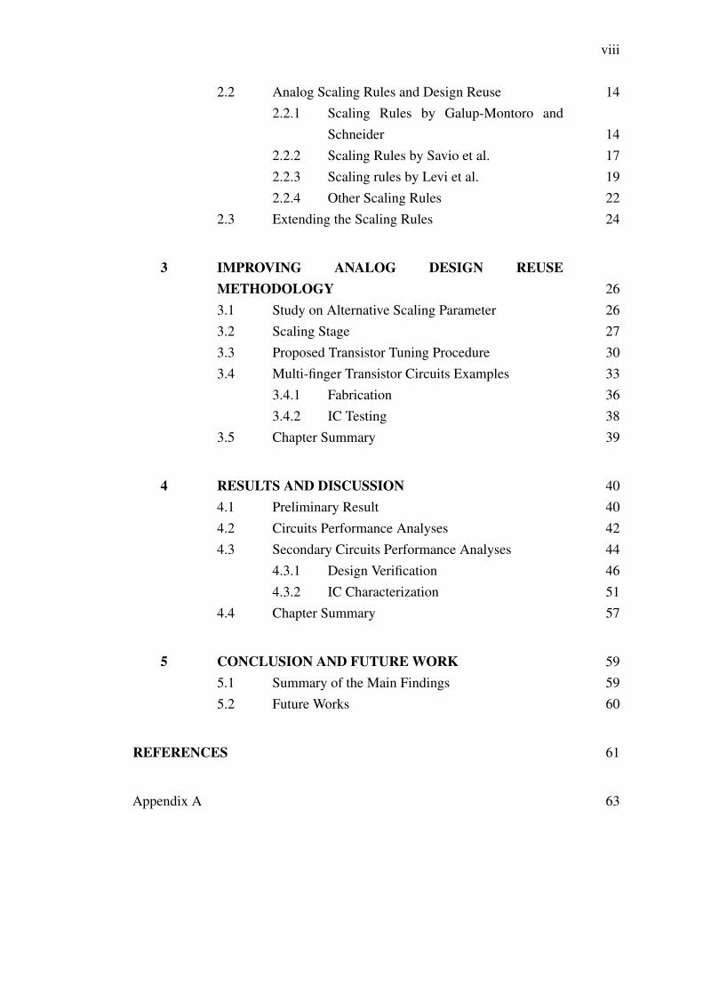
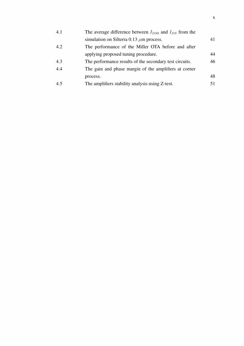
viii
2.2 Analog Scaling Rules and Design Reuse 142.2.1 Scaling Rules by Galup-Montoro and
Schneider 142.2.2 Scaling Rules by Savio et al. 172.2.3 Scaling rules by Levi et al. 192.2.4 Other Scaling Rules 22
2.3 Extending the Scaling Rules 24
3 IMPROVING ANALOG DESIGN REUSEMETHODOLOGY 263.1 Study on Alternative Scaling Parameter 263.2 Scaling Stage 273.3 Proposed Transistor Tuning Procedure 303.4 Multi-finger Transistor Circuits Examples 33
3.4.1 Fabrication 363.4.2 IC Testing 38
3.5 Chapter Summary 39
4 RESULTS AND DISCUSSION 404.1 Preliminary Result 404.2 Circuits Performance Analyses 424.3 Secondary Circuits Performance Analyses 44
4.3.1 Design Verification 464.3.2 IC Characterization 51
4.4 Chapter Summary 57
5 CONCLUSION AND FUTURE WORK 595.1 Summary of the Main Findings 595.2 Future Works 60
REFERENCES 61
Appendix A 63

ix
LIST OF TABLES
TABLE NO. TITLE PAGE
2.1 The scaling rules proposed by Galup-Montoro andSchneider. 14
2.2 The results of the scaling work by Galup-Montoro andSchneider. 15
2.3 The improved scaling rules proposed byGalup-Montoro et al. 16
2.4 The results of improved scaling rules byGalup-Montoro et al. 16
2.5 The scaling rules proposed by Savio et al. 182.6 The results of the scaling work by Savio et al. 182.7 The improved scaling rules by Savio et al. 192.8 Three case studies of scaling rules by Levi at al. 202.9 The scaling rules proposed by Levi et al. 212.10 The results of the scaling work (Case-A). 212.11 The transistor sizing for the case study (Case-A). 222.12 The scaling rules proposed by Yang et al. 232.13 Summary of the previous works on scaling rules. 253.1 The preliminary test circuit variables and parameters. 273.2 Design parameters for the Miller OTA. 283.3 Scaling parameters for Silterra CMOS
0.18 µm and 0.13 µm technologies. 283.4 Simplified scaling rules for Silterra CMOS
0.18 µm and 0.13 µm technologies. 293.5 Transistor sizing (W/L) of the Miller OTA for long-
channel and short-channel examples. 293.6 The output biasing voltage of the Miller OTA. 303.7 Summary of test circuits Amp-A and Amp-B. 343.8 The simplified scaling parameter for Silterra
technologies. 343.9 The transistor sizing for secondary test circuits. 36
x
4.1 The average difference between IDS0 and IDS from thesimulation on Silterra 0.13 µm process. 41
4.2 The performance of the Miller OTA before and afterapplying proposed tuning procedure. 44
4.3 The performance results of the secondary test circuits. 464.4 The gain and phase margin of the amplifiers at corner
process. 484.5 The amplifiers stability analysis using Z-test. 51

xi
LIST OF FIGURES
FIGURE NO. TITLE PAGE
1.1 Flowchart of the research methodology. 52.1 Power consumption with technology scaling for analog
circuits with fixed speed and accuracy requirements. 82.2 The effect of technology migration on power consump-
tion at a constant performance. 92.3 The transistor intrinsic gain for 180 nm, 130 nm and
90 nm technologies. 102.4 The effect of technology scaling on leakage current. 112.5 Velocity saturation in short-channel transistor. 122.6 The number of design rules for various technology
nodes. 132.7 The Miller OTA test circuit (Galup-Montoro). 152.8 The Miller OTA test circuit (Savio et al.). 172.9 The OTA test circuit (Levi et al.). 202.10 Operational amplifier sizing process flow. 243.1 The test circuit to extract IDS-VDS relationship. 263.2 The primary test circuit, a Miller OTA. 273.3 The flowchart of the scaling and proposed tuning stages
and its related reference and equations. 333.4 The Amp-B with split-length PMOS transistors. 353.5 The split-length transistor idea. 353.6 The top-level layout of the chip. 373.7 The ESD protection circuit on the bond pads. 383.8 IC testing and measurement on the breadboard. 394.1 The NMOS transistor I-V curve for IDS0, IDS1 and IDS2
at VGS = 0.7 V. 414.2 The effect of biasing point VY on (a) gain
(b) phase margin. 434.3 The gain-bandwidth curves of the original design and
migrated design with the proposed tuning applied. 45

xii
4.4 The corner analyses for (a) Amp-A (b) Amp-B onSilterra 0.18 µm process. 47
4.5 The Monte Carlo simulation results of the phase marginof Amp-A for (a) 0.18 µm process (b) 0.13 µm process. 49
4.6 The Monte Carlo simulation results of the phase marginof Amp-B for (a) 0.18 µm process (b) 0.13 µm process. 50
4.7 Amp-A input-output signals response on-wafer test. 524.8 Amp-B input-output signals response on-wafer test. 534.9 The breadboard testing circuit. 544.10 Amp-A input-output signal response for breadboard test. 564.11 Amp-B input-output signal response for breadboard test. 57
xiii
LIST OF ABBREVIATIONS
AC - Alternating Current
ADC - Analog-to-Digital Converter
AMS - Analog Mixed Signal
BSIM - Berkeley Short-channel IGFET Model
CEDEC - Collaborative Microelectronic Design Excellence Centre
CMOS - Complementary Metal Oxide Semicodictor
COMDIAC - Compilateur de Dispositifs Actifs
DC - Direct Current
DIBL - Drain Induced Barrier Lowering
EDA - Electronic Design Aided
ESD - Electrostatic Discharge
FF - Fast-PMOS Fast-NMOS
GBW - Gain-Bandwidth
I/O - Input-Output
IC - Integrated Circuit
MOS - Metal-Oxide-Semiconductor
MOSFET - Metal Oxide Semiconductor Field Effect Transistor
NML - Non-Minimum Length
NMOS - N-type Metal Oxide Semiconductor
n-MOSFET - N-type MOSFET
OTA - Output Transconductance Amplifier
PMOS - P-type Metal Oxide Semiconductor
p-MOSFET - P-type MOSFET
SCE - Short-Channel Effect
SI - Strong Inversion
SoC - System-on-Chip
SPICE - Simulation Program for Integrated Circuits Emphasis
SS - Slow-PMOS Slow-NMOS

xiv
TT - Typical-PMOS Typical-NMOS
USM - Universiti Sains Malaysia
Vpp - Voltage peak-to-peak
W/L - Width-to-Length
WI - Weak Inversion

xv
LIST OF SYMBOLS
W – Width of transistor
L – Length of transistor
ID, IDS – Transistor drain-to-source current
VDD – Power supply voltage
VDS – Transistor drain-to-source voltage
VGS – Transistor gate-to-source voltage
VEG – Effective gate voltage
VTh – Transistor threshold voltage
gm – Transconductance of transistor
P – Power consumption
tox – Transistor oxide thickness
gds – Transistor drain-to-source transconductance
A,AV – Voltage gain
rds – Transistor drain-to-source resistance
fT – Transition frequency
Cgs – Transistor gate-to-source capacitance
Cox – Transistor oxide capacitance
CC – Compensation capacitor
CL – Load capacitor
VE – Early voltage
µ – Electron mobility
KL – Gate length scaling parameter
KW – Width scaling parameter
KwN – Width scaling parameter for n-MOSFET
KwP – Width scaling parameter for p-MOSFET
KV – Power supply scaling parameter
Kox – Oxide capacitance scaling parameter
xvi
KoxN – Oxide capacitance scaling parameter for n-MOSFET
KoxP – Oxide capacitance scaling parameter for p-MOSFET
KE – Early voltage scaling parameter
Kµ – Electron mobility scaling parameter
KµN – Electron mobility scaling parameter for n-MOSFET
KµP – Electron mobility scaling parameter for p-MOSFET
Kn – Slope scaling parameter
KC – Load capacitance scaling parameter
KI – Current scaling parameter
if – Forward inversion level
ir – Reverse inversion level
εox – Oxide relative permittivity
Wf – Finger width of transistor
nf – Number of finger of transistor
λ – Channel modulation parameter
σ – Standard deviation
–
Ahmad
Line
Ahmad
Rectangle

xvii
LIST OF APPENDICES
APPENDIX TITLE PAGE
A LIST OF PUBLICATIONS 63
CHAPTER 1
INTRODUCTION
This research work studies the issues and challenges of analog CMOS designreuse methodology. The main objective is to formulate an analog design reusemethodology which is compatible with short-channel CMOS design. This workproposes a second-stage tuning methodology for analog design reuse to increase theaccuracy in maintaining the original analog circuit performance for short-channeldevice. Silterra CMOS 0.18 µm and 0.13 µm fabrication processes are used in thestudy. The study is divided into two parts. The first part is to study the impact ofprocess scaling on analog and mixed-signal designs. The second part is to formulatean extension of existing analog design reuse methodology for short-channel analogdesign application, and to rectify gain degradation problem which is usually associatedwith short-channel transistor.
1.1 Scaling Rules and Design Reuse
Scaling rules are used to provide new transistor sizing while maintainingthe original circuit performance during process migration. The performance of ananalog circuit is highly dependent on process parameters. Therefore, it is importantto study the relationship between process parameters and circuit performance tofacilitate analog design reusability in various fabrication processes. The significantadvantage of having systematic analog design reuse methodology is the shorter timeneeded for circuit rescaling compared to complete circuit redesign to meet the originalspecification.
Systematic analog design reuse methodology can assist designer in maintaininganalog circuit performance in different processes. Digital circuits are easier to scaleand usually can be done by automation, thus much less complex migration process
2
involved compared to analog circuits. As the analog design complexity keep growing,systematic reuse methodology for analog circuits can help to reduce the design time.Existing scaling rules for analog design reuse have to sacrifice some performancematrics in order to maintain the more important matrics [1, 2, 3, 4, 5]. Furthermore,the scaling rules were tested to MOS field effect transistors (MOSFETs) with the gate-length equal to few micrometers [2, 4]. Therefore, this research proposes a tuningprocedure to increase the accuracy of the design scaling, and it is compatible withshort-channel design.
Emerging short-channel effects and leakage current contribute to the latestanalog design challenges in deep submicron process [6]. Moreover, power supplyscaling is the biggest challenge [7]. These design issues also contribute to the problemsof the analog circuit performance when migrating into deep submicron process suchas:
• Reduction in transistor intrinsic gain due to velocity saturation [8, 6]
• Reduction in signal to noise ratio as a result of using low supply voltage andultra thin gate oxide [6]
• Higher signal distortion for transistor operating in weak inversion [8]
Due to high design sensitivity in deep submicron process, designer is now relying evenmore on simulator program and accurate device modeling [8]. Hundreds of parametersare defined to describe short-channel transistor behaviour in various biasing points,making hand calculation even more complex, time consuming and less reliable. Thegrowing design complexity reflects growing analog design time which affect the time-to-market.
1.2 Problem Statement
When one design migrates to a smaller process compared to its original size, itis expected that the performance of the design will be preserved if not better. However,previous works have proven that preserving all design specifications in a migrateddesign is not a straightforward process. Many reports [2, 3, 4, 5, 9, 10, 11] havehighlighted that one may be able to preserve some of the specifications but not all. Thisissue is further aggravates when it involves migration to the deep submicron region.

3
Scaling rules can maintain gain-bandwidth and dynamic range of anoperational amplifier during migration [1, 2]. However, the power consumption maydoubled or the silicon area can be much larger compared to the original design [1, 2].Another work with modified scaling rules and a follow-on automatic tuning stage resultin significant power reduction but at a cost of few times bigger silicon area comparedto the original design [3, 4].
Channel-scaling rules derived from the MOSFET level-1 current equation [5,11] resulted in lower power consumption and smaller area while maintaining the gain,bandwidth and phase margin. However, in the smallest fabrication process tested(0.12 micron), the amplifier gain is degraded [5]. Besides, all earlier works [1, 2, 5, 11]were tested on considerable long-channel MOSFET. As technology progresses into thedeep submicron technology, consideration of short-channel MOSFET in analog designmigration must be taken into account.
The degradation of transistor intrinsic gain is one of the prominent designproblems in short-channel analog design [8]. Amplifier gain which is widelyconsidered as the most important performance in any analog amplifier is directlyrelated to the intrinsic gain. This research aims to rectify the amplifier gain degradationproblem in analog design migration which becomes more significance for migrationinto deep submicron process. Hence, the design reuse methodology is further enhancedby extending the compatibility of the scaling process with the short-channel analogdesign.
1.3 Objectives
Based on the problem statement, this research work aims to achieve thefollowing objectives:
i. To propose a tuning procedure for analog design reuse which can be appliedto both short-channel and long-channel MOSFETs. The tuning procedure cancompliment existing scaling works which are more suitable for long-channeltransistors.
ii. To preserve the operational amplifier performance (gain, bandwidth and phasemargin) during process migration at reduced power consumption and siliconarea.

4
1.4 Scope of Work
This research aims to upgrade existing scaling rules with the proposed tuningprocedure. The proposed tuning procedure is compatible with both long-channel andshort-channel analog designs and able to maintain circuit performance during theprocess migration. Operational transconductance amplifier (OTA) circuits are usedas the test circuits. The circuits are designed and characterized by using Cadenceelectronic design automation (EDA) on Silterra 0.18 µm process. Using scaling rulesproposed in [5], the designs are migrated to 0.13 µm Silterra process. The proposedtuning procedure is then applied to the migrated designs. The significant of the tuningprocedure is presented by tables and graphs generated by Matlab software. Selecteddesigns are sent for fabrication at Silterra Malaysia and the IC is characterized usingon-wafer test by Collaborative Microelectronic Design Excellence Centre (CEDEC) ofUniversiti Sains Malaysia (USM). Next, the IC is packaged, a test circuit is constructedusing off-chip components and characterized using Agilent test and measurementinstruments.
1.5 Methodology
This research is divided into three phases as shown in Figure 1.1. The firstphase is the background study of scaling rules and analog scaling challenges. Then,problem statement is constructed based on the study.
The second phase started with a case study to formulate the design reusemethodology. Based on preliminary results from a case study, this research decidedto propose a tuning procedure to achieve the objectives. The idea of preserving theoutput swing during design migration is translated into equations which guide theentire tuning process. This phase involves the circuit design and design migrationstages. During these stages, operational amplifier circuits are designed on 0.18 µmand then characterized. Then the same designs are migrated to 0.13 µm processand characterized. Performance degradation of the migrated design in the 0.13 µmespecially on short-channel design leads to the construction of tuning methodologystage. In this stage, a DC output voltage scaling is proposed and related equations arederived to adjust the output voltage of the two-stage analog amplifier. The last stage istesting the methodology on another amplifier designs to evaluate the performance ofthe proposed tuning procedure. Corner analysis and Monte Carlo simulation are used

5
to measure the reliability of the designs.
In the second phase, similar OTA circuits used in previous literature [1, 2, 3,4, 5, 11] are adopted as the test circuits. They are constructed using short-channelor long-channel MOSFETs to represent two cases along with Miller compensationcircuit to realize high output gain. Five key performance indicators are considered tobe maintained during the design migration: voltage gain, bandwidth, phase margin,power consumption, and silicon area. The proposed tuning procedure aims to maintainthe key performance during the process migration from 0.18 µm to 0.13 µm processesat a minimal trade-off. In addition, amplifier circuits with multi-finger and split-lengthtransistors are used to verify the methodology.
The third phase of the research is to fabricate the design and characterized thephysical IC. The layout from the selected design is prepared for fabrication by SilterraMalaysia using 0.18 µm CMOS process. The physical design is then characterizedusing on-wafer test and breadboard test. The related problems and limitations arediscussed and analyzed in Chapter 4.
Phase I Phase II Phase III
Literature review
Case study Methodology testing
Physical design
Circuit design & simulation Construct tuning
procedure Fabrication & characterization
Figure 1.1: Flowchart of the research methodology.
1.6 Contributions
This research work contributes on an improved design reuse methodology thatis suitable for both long- and short-channels transistors. Specifically, the contributionof the research are as follow:

6
i. The preservation of the output swing is taken into consideration which leads tothe tuning procedure based on the scaled value of DC output voltage. This helpsmaintain the voltage gain and phase margin.
ii. Instead of tuning both width and length of the transistor, this thesis proposesthe tuning of the width to adjust the DC output voltage. This is to ensure thetransistor threshold voltage is maintained. Another advantage of scaling thewidth is to avoid short-channel effects (SCE) and drain-induced barrier lowering(DIBL) from being significantly modified.
1.7 Structure of Thesis
The thesis is organized into five chapters. The rest of the chapters are as follow.
Chapter 2 discusses the analog design migration challenges into deepsubmicron technology and existing scaling rules and its theories, advantages andlimitations.
Chapter 3 presents the design scaling and the proposed tuning procedure basedon DC output scaling. It is divided into four sections: the preliminary experiment, thedesign scaling, the proposed tuning procedure and the proposed tuning for multi-fingertransistors.
Chapter 4 presents the performance analysis of the proposed tuning procedurefor all circuit examples and the result of the physical design characterization.
Finally, conclusion and suggestions for future works are presented in Chapter 5.

REFERENCES
1. Galup-Montoro, C. and Schneider, M. Resizing Rules for The Reuse of MOSAnalog Designs. Manaus: Proceedings of the 13th Symposium on Integrated
Circuits and Systems Design. 2000. 89–93.
2. Galup-Montoro, C., Schneider, M. and Coitinho, R. Resizing Rules for MOSAnalog-Design Reuse. IEEE Design & Test of Computers, 2002. 19(2): 50–58.
3. Savio, A., Colalongo, L., Kovacs-Vajna, Z. and Quarantelli, M. Scaling Rulesand Parameter Tuning Procedure for Analog Design Reuse in TechnologyMigration. Proceedings of the International Symposium on Circuits and
Systems. 2004. V–117–V–120 Vol. 5.
4. Savio, A., Colalongo, L., Quarantelli, M. and Kovacs-Vajna, Z. AutomaticScaling Procedures for Analog Design Reuse. IEEE Transactions on Circuits
and Systems I, 2006. 53(12): 2539–2547.
5. Levi, T., Tomas, J., Lewis, N. and Fouillat, P. A CMOS Resizing Methodologyfor Analog Circuits. IEEE Design & Test of Computers, 2009. 26(1): 78–87.
6. Sansen, W. Analog Design Challenges in Nanometer CMOS Technologies.IEEE Asian Solid-State Circuits Conference. 2007. 5–9.
7. Annema, A., Nauta, B., van Langevelde, R. and Tuinhout, H. Analog Circuitsin Ultra-Deep-Submicron CMOS. IEEE Journal of Solid-State Circuits, 2005.40(1): 132–143.
8. Murmann, B., Nikaeen, P., Connelly, D. J. and Dutton, R. W. Impact of Scalingon Analog Performance and Associated Modeling Needs. IEEE Transactions
on Electron Devices, 2006. 53(9): 2160–2167.
9. Yang, T., Gao, M., Wu, S. and Guo, D. A New Reuse Method of AnalogCircuit Design for CMOS Technology Migration. International Conference on
Anti-Counterfeiting Security & Identification in Communication. 2010.112–115.
10. Acosta, R., Silveira, F. and Aguirre, P. Experiences on Analog CircuitTechnology Migration and Reuse. Proceedings of the 15th Symposium on
Integrated Circuits and Systems Design. 2002. 169–174.

62
11. Levi, T., Lewis, N., Tomas, J. and Fouillat, P. Scaling Rules for MOS AnalogDesign Reuse. Proceedings of the International Conference of Mixed Design
of Integrated Circuits and System. 2006. 378–382.
12. Gielen, G. and Dehaene, W. Analog and Digital Circuit Design in 65 nmCMOS: End of The Road? Proceedings in Europe on Design, Automation and
Test. 2005. 37–42 Vol. 1.
13. Garg, M., Suryagandh, S. and Woo, J. Scaling Impact on Analog Performanceof Sub-100nm MOSFETs for Mixed Mode Applications. European
Conference on Solid-State Device Research. 2003. 371–374.
14. Borkar, S. Design Challenges of Technology Scaling. IEEE Micro, 1999.19(4): 23–29.
15. Gray, P., Hurst, P., Meyer, R. and Lewis, S. Analysis and Design of Analog
Integrated Circuits. 5th ed. John Wiley & Sons. 2010.
16. Lewyn, L. and Williams, N. Is A New Paradigm for Nanoscale Analog CMOSDesign Needed? Proceedings of the IEEE, 2011. 99(1): 3–6.
17. Saleh, R., Wilton, S., Mirabbasi, S., Hu, A., Greenstreet, M., Lemieux, G.,Pande, P. P., Grecu, C. and Ivanov, A. System-on-Chip: Reuse and Integration.Proceedings of the IEEE, 2006. 94(6): 1050–1069.
18. Vittoz, E. Future of Analog in The VLSI Environment. IEEE International
Symposium on Circuits and Systems. 1990. 1372–1375.
19. Cunha, A., Schneider, M. and Galup-Montoro, C. An MOS Transistor Modelfor Analog Circuit Design. IEEE Journal of Solid-State Circuits, 1998. 33(10):1510–1519.
20. Press, W., Teukolsky, S., Vetterling, W. and Flannery, B. Numerical Recipes
in C++: The Art of Scientific Computing. Cambridge University Press. 2002.
21. Dessouky, M., Kaiser, A., Lou, M. and Greiner, A. Analog Design for Reuse- Case Study: Very Low-Voltage Sigma-Delta Modulator. Proceedings onDesign, Automation and Test. 2001. ISBN 0-7695-0993-2. 353–360.
22. Porte, J. COMDIAC: Compilateur de Dispositifs Actifs, reference manual.Ecole Nationale Supérieure des Télécommunications, Paris, France, 1997.
23. Morshed, T. et al. BSIM4.6.4 MOSFET Model-User’s Manual. University ofCalifornia, Berkeley. 2009.
24. Taherzadeh, S. and Hamoui, A. A 1-V Process-Insensitive Current-ScalableTwo-Stage Opamp With Enhanced DC Gain and Settling Behavior in 65-nmDigital CMOS. IEEE Journal of Solid-State Circuits, 2011. 46(3): 660–668.