SOLIDS AND SEMICONDUCTOR DEVICES - III 1.Junction Transistor 2.NPN and PNP Transistor Symbols...
22
SOLIDS AND SEMICONDUCTOR DEVICES - III 1. Junction Transistor 2. NPN and PNP Transistor Symbols 3. Action of NPN Transistor 4. Action of PNP Transistor 5. Transistor Characteristics in Common Base Configuration 6. Transistor Characteristics in Common Emitter Configuration 7. NPN Transistor Amplifier in Common Base Configuration 8. PNP Transistor Amplifier in Common Base Configuration 9. Various Gains in Common Base Amplifier 10.NPN Transistor Amplifier in Common Emitter Configuration 11.PNP Transistor Amplifier in Common Emitter Configuration 12.Various Gains in Common Emitter Amplifier 13.Transistor as an Oscillator
-
Upload
clyde-richardson -
Category
Documents
-
view
271 -
download
4
Transcript of SOLIDS AND SEMICONDUCTOR DEVICES - III 1.Junction Transistor 2.NPN and PNP Transistor Symbols...
SOLIDS AND SEMICONDUCTOR DEVICES - III
1. Junction Transistor
2. NPN and PNP Transistor Symbols
3. Action of NPN Transistor
4. Action of PNP Transistor
5. Transistor Characteristics in Common Base Configuration
6. Transistor Characteristics in Common Emitter Configuration
7. NPN Transistor Amplifier in Common Base Configuration
8. PNP Transistor Amplifier in Common Base Configuration
9. Various Gains in Common Base Amplifier
10.NPN Transistor Amplifier in Common Emitter Configuration
11.PNP Transistor Amplifier in Common Emitter Configuration
12.Various Gains in Common Emitter Amplifier
13.Transistor as an Oscillator
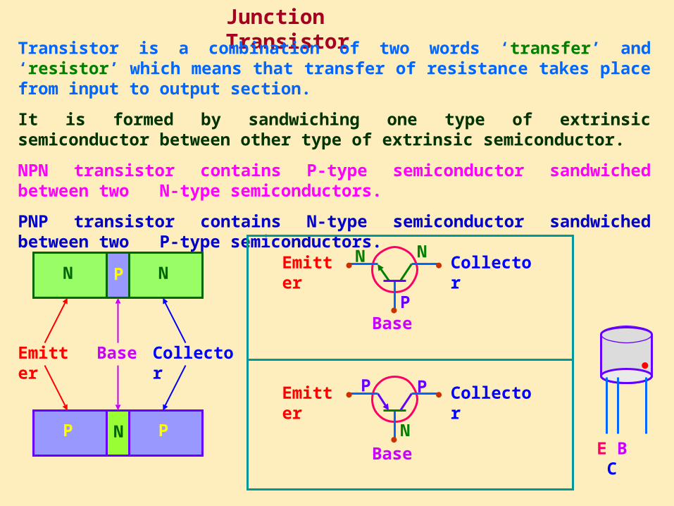
Junction Transistor
Transistor is a combination of two words ‘transfer’ and ‘resistor’ which means that transfer of resistance takes place from input to output section.
It is formed by sandwiching one type of extrinsic semiconductor between other type of extrinsic semiconductor.
NPN transistor contains P-type semiconductor sandwiched between two N-type semiconductors.
PNP transistor contains N-type semiconductor sandwiched between two P-type semiconductors.
P NN
N PP
●●
●
●●
●
Emitter Base Collector
Emitter
Base
Collector
Emitter
Base
Collector
N N
P
P P
N
●
E B C
Action of NPN Transistor
P N
-
-
-
Veb
+
+
+
+
+
+
+
+
+
+
+
+
+
+
+
+
+
+
+
+
+
+
+
+
Vcb
N
E
B
C
●●
●
E
B
C
N N
P
Veb Vcb
Ie Ib
Ic
IeIb Ic
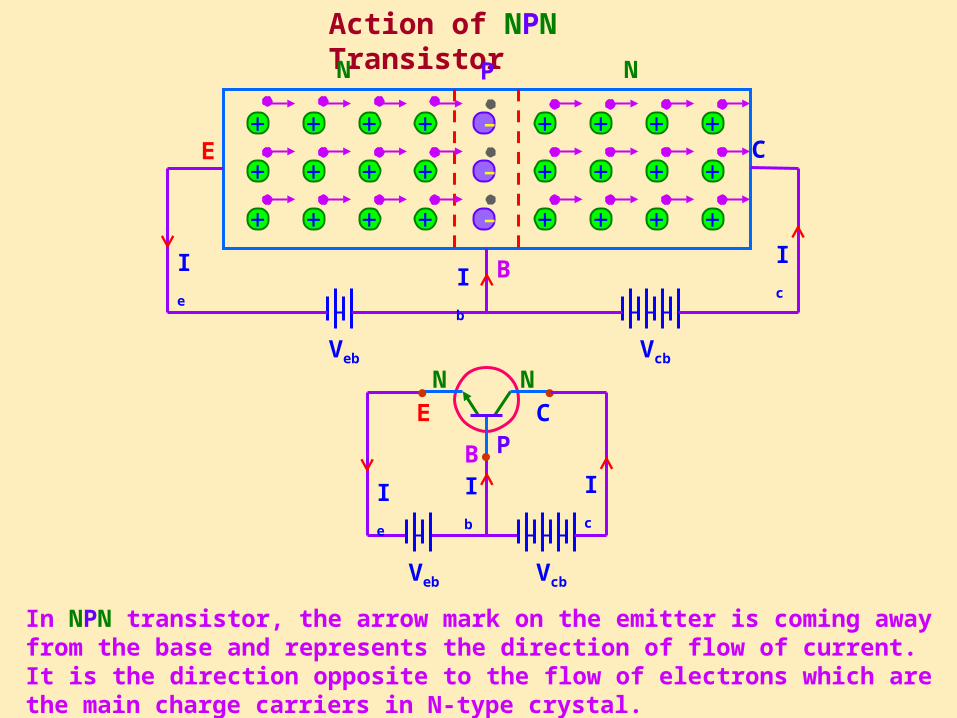
In NPN transistor, the arrow mark on the emitter is coming away from the base and represents the direction of flow of current. It is the direction opposite to the flow of electrons which are the main charge carriers in N-type crystal.
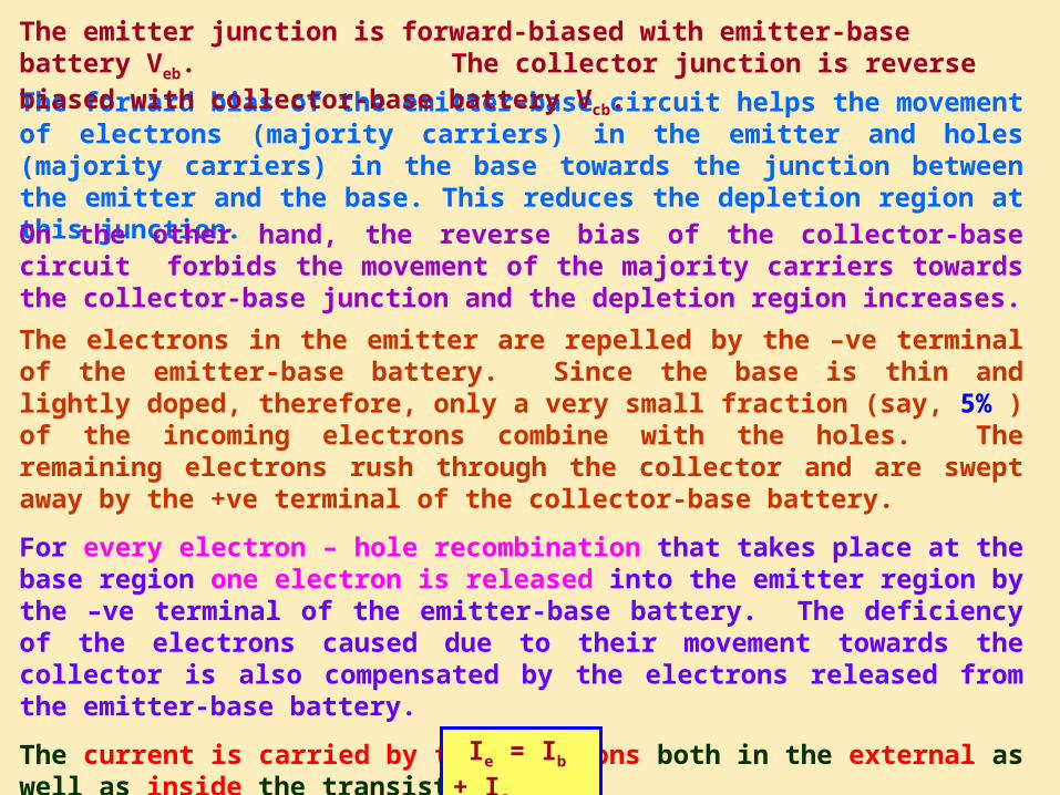
The electrons in the emitter are repelled by the –ve terminal of the emitter-base battery. Since the base is thin and lightly doped, therefore, only a very small fraction (say, 5% ) of the incoming electrons combine with the holes. The remaining electrons rush through the collector and are swept away by the +ve terminal of the collector-base battery.
For every electron – hole recombination that takes place at the base region one electron is released into the emitter region by the –ve terminal of the emitter-base battery. The deficiency of the electrons caused due to their movement towards the collector is also compensated by the electrons released from the emitter-base battery.
The current is carried by the electrons both in the external as well as inside the transistor.
Ie = Ib + Ic
The forward bias of the emitter-base circuit helps the movement of electrons (majority carriers) in the emitter and holes (majority carriers) in the base towards the junction between the emitter and the base. This reduces the depletion region at this junction. On the other hand, the reverse bias of the collector-base circuit forbids the movement of the majority carriers towards the collector-base junction and the depletion region increases.
The emitter junction is forward-biased with emitter-base battery Veb. The collector junction is reverse biased with collector-base battery Vcb.
Action of PNP Transistor:
P N
Veb
+
+
+
-
-
-
Vcb
E
B
C
●●
●
E
B
CP P
N
Veb Vcb
Ie Ib
Ic
IeIb Ic
-
-
-
-
-
-
-
-
-
-
-
-
-
-
-
-
-
-
-
-
-
P
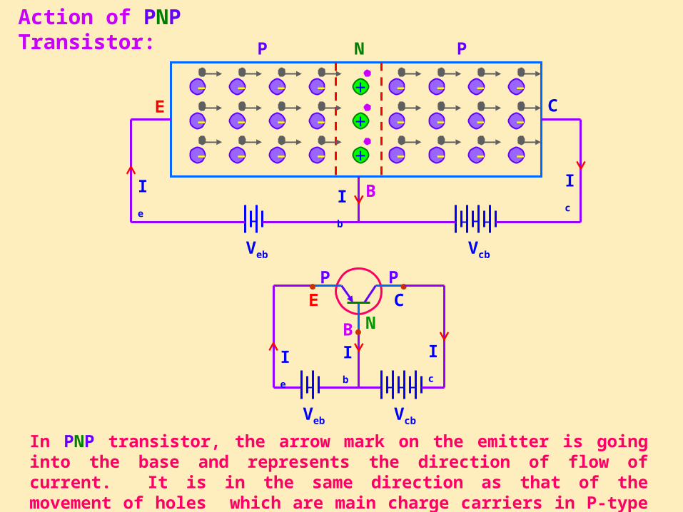
In PNP transistor, the arrow mark on the emitter is going into the base and represents the direction of flow of current. It is in the same direction as that of the movement of holes which are main charge carriers in P-type crystal.
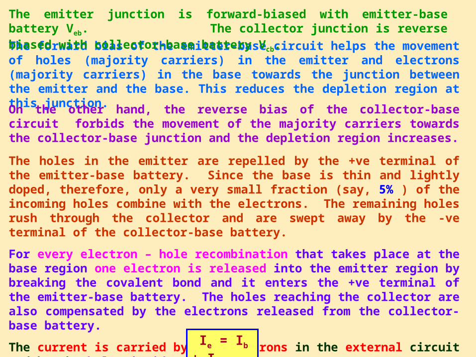
The holes in the emitter are repelled by the +ve terminal of the emitter-base battery. Since the base is thin and lightly doped, therefore, only a very small fraction (say, 5% ) of the incoming holes combine with the electrons. The remaining holes rush through the collector and are swept away by the -ve terminal of the collector-base battery.
For every electron – hole recombination that takes place at the base region one electron is released into the emitter region by breaking the covalent bond and it enters the +ve terminal of the emitter-base battery. The holes reaching the collector are also compensated by the electrons released from the collector-base battery.
The current is carried by the electrons in the external circuit and by the holes inside the transistor.
Ie = Ib + Ic
The forward bias of the emitter-base circuit helps the movement of holes (majority carriers) in the emitter and electrons (majority carriers) in the base towards the junction between the emitter and the base. This reduces the depletion region at this junction.
On the other hand, the reverse bias of the collector-base circuit forbids the movement of the majority carriers towards the collector-base junction and the depletion region increases.
The emitter junction is forward-biased with emitter-base battery Veb. The collector junction is reverse biased with collector-base battery Vcb.
mA
+
mA
+E
B
CP P
N
+Veb
●●
●
Vcb
+
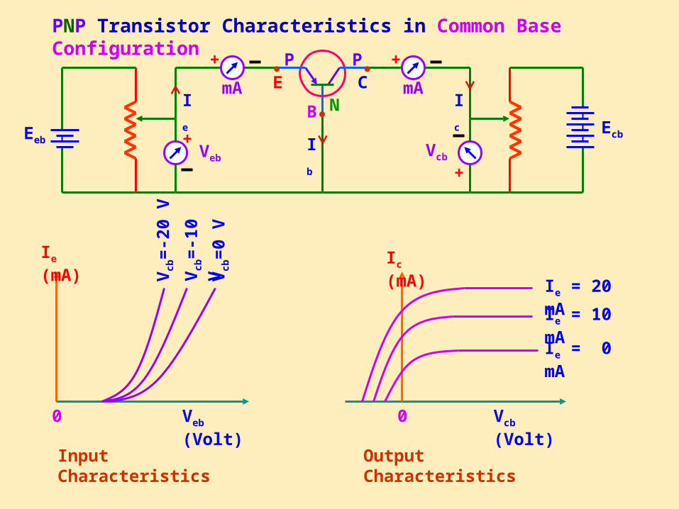
PNP Transistor Characteristics in Common Base Configuration
Ie
Ib
EebEcb
Ic
Ie (mA)
Vcb
=0
V
Vcb
=-1
0 V
Vcb
=-2
0 V
0
Input Characteristics Output Characteristics
Vcb (Volt)
Ic (mA)
Ie = 0 mA
Ie = 10 mA
Ie = 20 mA
0Veb (Volt)
μA
+mA
+
E
B
CP
P
N
Vbe
+
●●
●
Vce
+
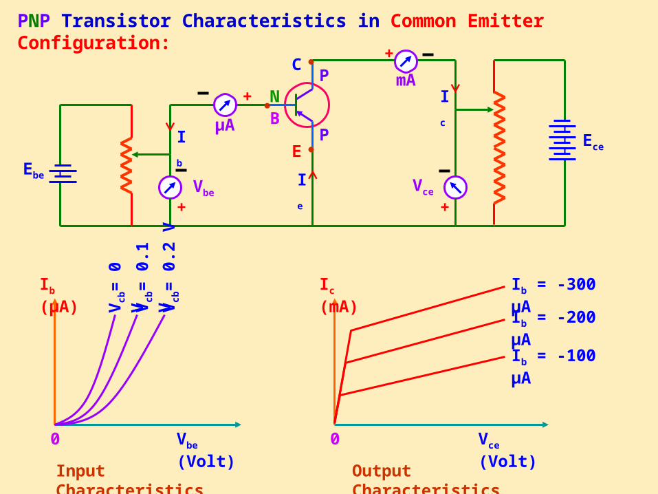
PNP Transistor Characteristics in Common Emitter Configuration:
Ib
Ie
Ebe
Ece
Ic
Ib (μA)
Vcb
= 0
.2 V
Vcb
= 0
.1 V
Vcb
= 0
V
0
Input Characteristics Output Characteristics
Vce (Volt)
Ic (mA)
Ib = -100 μA
0Vbe (Volt)
Ib = -200 μA
Ib = -300 μA
●
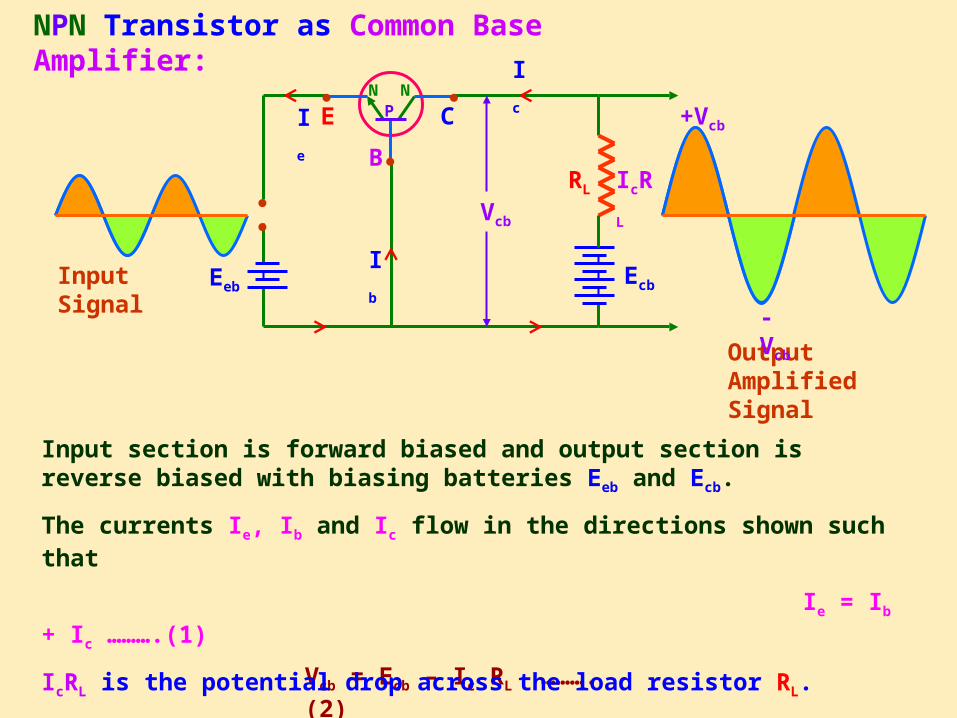
NPN Transistor as Common Base Amplifier:
E
B
CN N
PIe
Ib
Ic●●
●
Eeb
●Vcb
Ecb
RL
Input Signal
Output Amplified Signal
IcRL
Vcb = Ecb – Ic RL ……….(2)
Input section is forward biased and output section is reverse biased with biasing batteries Eeb and Ecb.
The currents Ie, Ib and Ic flow in the directions shown such that
Ie = Ib + Ic ……….(1)
IcRL is the potential drop across the load resistor RL.
By Kirchhoff’s rule,
+Vcb
-Vcb
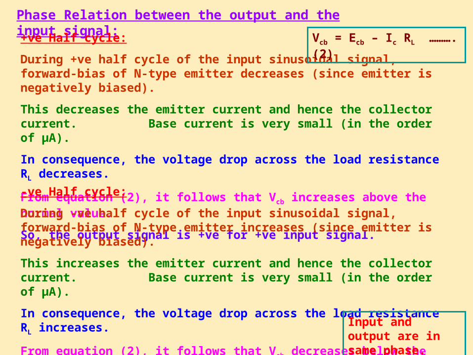
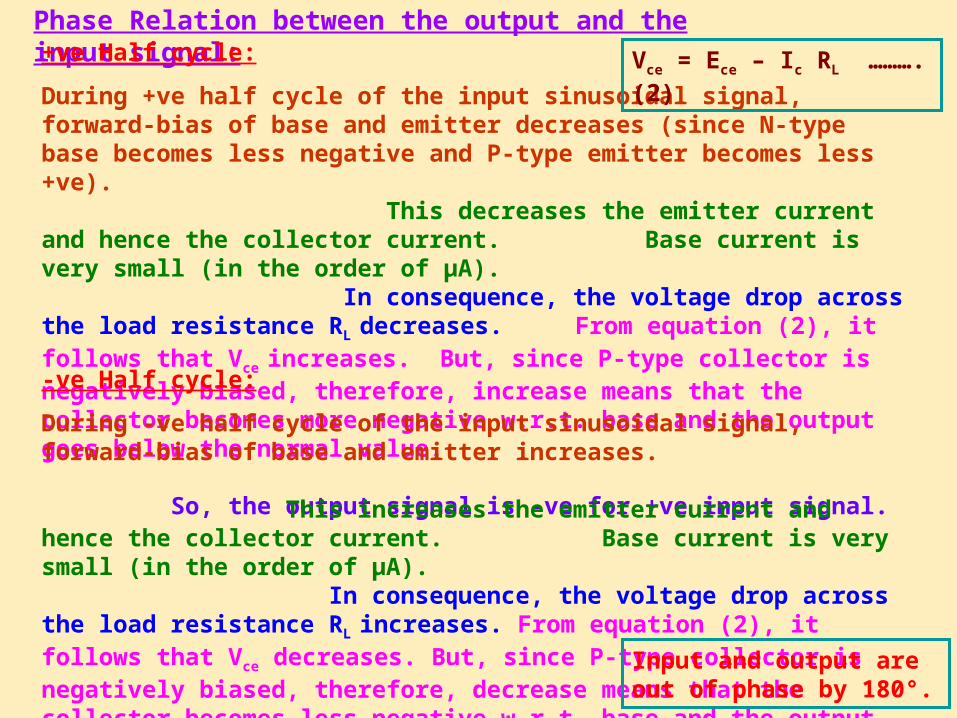
Phase Relation between the output and the input signal:
+ve Half cycle:
During +ve half cycle of the input sinusoidal signal, forward-bias of N-type emitter decreases (since emitter is negatively biased).
This decreases the emitter current and hence the collector current. Base current is very small (in the order of μA).
In consequence, the voltage drop across the load resistance RL decreases.
From equation (2), it follows that Vcb increases above the normal value.
So, the output signal is +ve for +ve input signal.-ve Half cycle:
During -ve half cycle of the input sinusoidal signal, forward-bias of N-type emitter increases (since emitter is negatively biased).
This increases the emitter current and hence the collector current. Base current is very small (in the order of μA).
In consequence, the voltage drop across the load resistance RL increases.
From equation (2), it follows that Vcb decreases below the normal value.
So, the output signal is -ve for -ve input signal.
Vcb = Ecb – Ic RL ……….(2)
Input and output are in same phase.
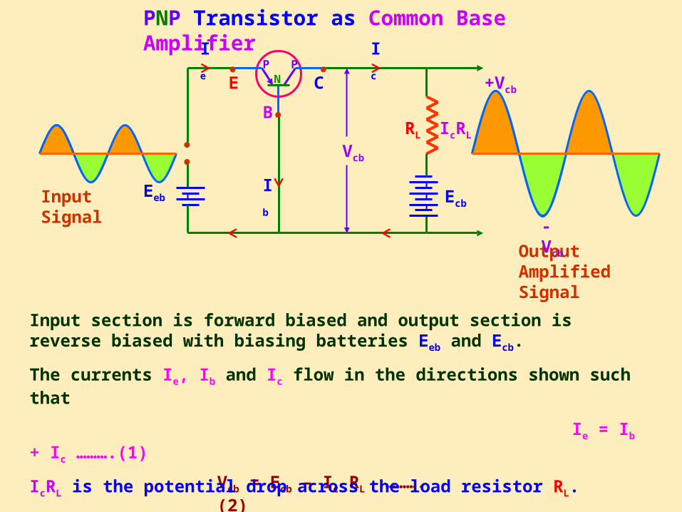
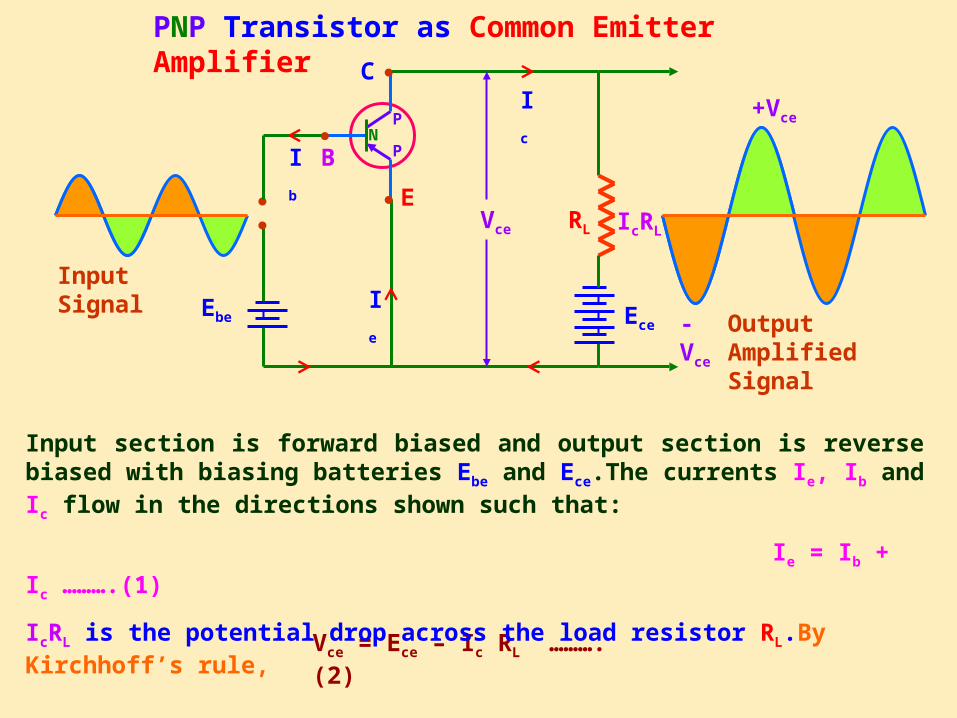
PNP Transistor as Common Base Amplifier
IbEeb
●● Vcb
Ecb
RL
●●
●
E
B
CP P
N
Input Signal
Output Amplified Signal
IcRL
Vcb = Ecb – Ic RL ……….(2)
Input section is forward biased and output section is reverse biased with biasing batteries Eeb and Ecb.
The currents Ie, Ib and Ic flow in the directions shown such that
Ie = Ib + Ic ……….(1)
IcRL is the potential drop across the load resistor RL.
By Kirchhoff’s rule,
Ie Ic
+Vcb
-Vcb
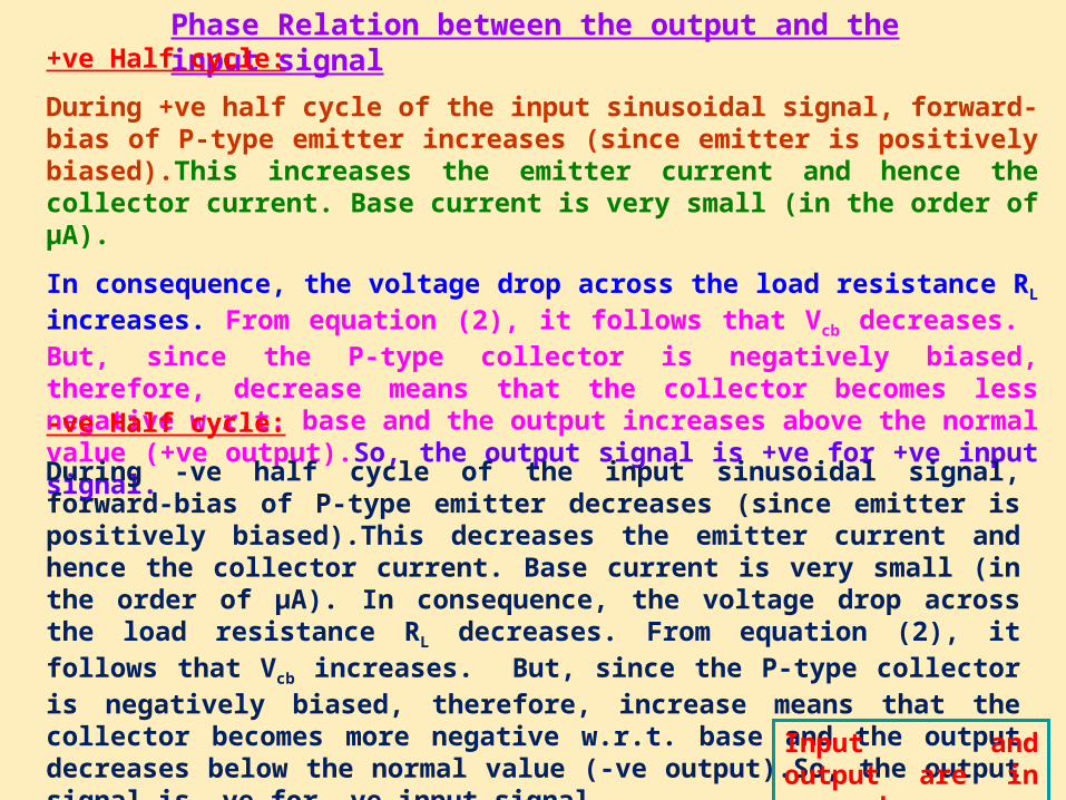
Phase Relation between the output and the input signal+ve Half cycle:
During +ve half cycle of the input sinusoidal signal, forward-bias of P-type emitter increases (since emitter is positively biased).This increases the emitter current and hence the collector current. Base current is very small (in the order of μA).
In consequence, the voltage drop across the load resistance RL increases. From equation (2), it follows that Vcb decreases. But, since the P-type collector is negatively biased, therefore, decrease means that the collector becomes less negative w.r.t. base and the output increases above the normal value (+ve output).So, the output signal is +ve for +ve input signal.-ve Half cycle:
During -ve half cycle of the input sinusoidal signal, forward-bias of P-type emitter decreases (since emitter is positively biased).This decreases the emitter current and hence the collector current. Base current is very small (in the order of μA). In consequence, the voltage drop across the load resistance RL decreases. From equation (2), it follows that Vcb increases. But, since the P-type collector is negatively biased, therefore, increase means that the collector becomes more negative w.r.t. base and the output decreases below the normal value (-ve output).So, the output signal is -ve for -ve input signal. Input and output
are in same phase.
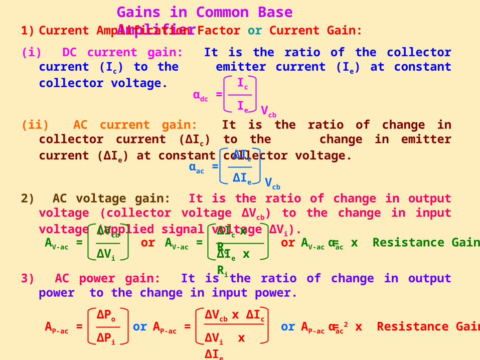
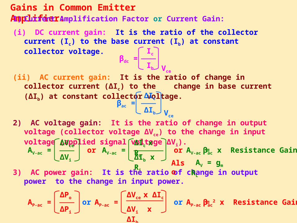
Gains in Common Base Amplifier1) Current Amplification Factor or Current Gain:
(i) DC current gain: It is the ratio of the collector current (Ic) to the emitter current (Ie) at constant collector voltage.
(ii) AC current gain: It is the ratio of change in collector current (ΔIc) to the change in emitter current (ΔIe) at constant collector voltage.
αdc = Ic
Ie Vcb
αac = ΔIc
ΔIe Vcb
2) AC voltage gain: It is the ratio of change in output voltage (collector voltage ΔVcb) to the change in input voltage (applied signal voltage ΔVi).
AV-ac = ΔVcb
ΔVi
AV-ac = αac x Resistance GainAV-ac = ΔIc x Ro
ΔIe x Ri
oror
3) AC power gain: It is the ratio of change in output power to the change in input power.
AP-ac = ΔPo
ΔPi
AP-ac = αac2 x Resistance Gainoror
ΔVcb x ΔIc
ΔVi x ΔIe
AP-ac =
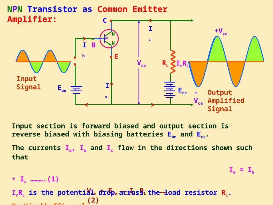
NPN Transistor as Common Emitter Amplifier:
Ie Ece
Vce RL
E
B
C
N
NP
●●
●
Ebe
●●
Input Signal
Output Amplified Signal
IcRL
Vce = Ece – Ic RL ……….(2)
Input section is forward biased and output section is reverse biased with biasing batteries Ebe and Ece.
The currents Ie, Ib and Ic flow in the directions shown such that
Ie = Ib + Ic ……….(1)
IcRL is the potential drop across the load resistor RL.
By Kirchhoff’s rule,
+Vce
-Vce
Ib
Ic
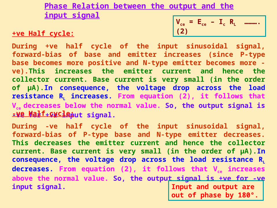
Phase Relation between the output and the input signal
+ve Half cycle:
During +ve half cycle of the input sinusoidal signal, forward-bias of base and emitter increases (since P-type base becomes more positive and N-type emitter becomes more -ve).This increases the emitter current and hence the collector current. Base current is very small (in the order of μA).In consequence, the voltage drop across the load resistance RL increases. From equation (2), it follows that Vce decreases below the normal value. So, the output signal is -ve for +ve input signal.
-ve Half cycle:
During -ve half cycle of the input sinusoidal signal, forward-bias of P-type base and N-type emitter decreases. This decreases the emitter current and hence the collector current. Base current is very small (in the order of μA).In consequence, the voltage drop across the load resistance RL decreases. From equation (2), it follows that Vce increases above the normal value. So, the output signal is +ve for -ve input signal.
Vce = Ece – Ic RL ……….(2)
Input and output are out of phase by 180°.
●
PNP Transistor as Common Emitter Amplifier
Ib
Ie
Ic
Vce
Ece
RL
E
B
C
P
PN
●●
●
Ebe
●
Input Signal
Output Amplified Signal
IcRL
Vce = Ece – Ic RL ……….(2)
Input section is forward biased and output section is reverse biased with biasing batteries Ebe and Ece.The currents Ie, Ib and Ic flow in the directions shown such that:
Ie = Ib + Ic ……….(1)
IcRL is the potential drop across the load resistor RL.By Kirchhoff’s rule,
+Vce
-Vce
Phase Relation between the output and the input signal:+ve Half cycle:
During +ve half cycle of the input sinusoidal signal, forward-bias of base and emitter decreases (since N-type base becomes less negative and P-type emitter becomes less +ve). This decreases the emitter current and hence the collector current. Base current is very small (in the order of μA). In consequence, the voltage drop across the load resistance RL decreases. From equation (2), it follows that Vce increases. But, since P-type collector is negatively biased, therefore, increase means that the collector becomes more negative w.r.t. base and the output goes below the normal value. So, the output signal is -ve for +ve input signal.-ve Half cycle:
During -ve half cycle of the input sinusoidal signal, forward-bias of base and emitter increases. This increases the emitter current and hence the collector current. Base current is very small (in the order of μA). In consequence, the voltage drop across the load resistance RL
increases. From equation (2), it follows that Vce decreases. But, since P-type collector is negatively biased, therefore, decrease means that the collector becomes less negative w.r.t. base and the output goes above the normal value. So, the output signal is +ve for -ve input signal.
Vce = Ece – Ic RL ……….(2)
Input and output are out of phase by 180°.
Gains in Common Emitter Amplifier:1) Current Amplification Factor or Current Gain:
(i) DC current gain: It is the ratio of the collector current (Ic) to the base current (Ib) at constant collector voltage.
(ii) AC current gain: It is the ratio of change in collector current (ΔIc) to the change in base current (ΔIb) at constant collector voltage.
βdc = Ic
Ib Vce
βac = ΔIc
ΔIb Vce
2) AC voltage gain: It is the ratio of change in output voltage (collector voltage ΔVce) to the change in input voltage (applied signal voltage ΔVi).
AV-ac = ΔVce
ΔVi
AV-ac = βac x Resistance GainAV-ac = ΔIc x Ro
ΔIb x Ri
oror
3) AC power gain: It is the ratio of change in output power to the change in input power.
AP-ac = ΔPo
ΔPi
AP-ac = βac2 x Resistance Gainoror
ΔVce x ΔIc
ΔVi x ΔIb
AP-ac =
AV = gm RLAlso
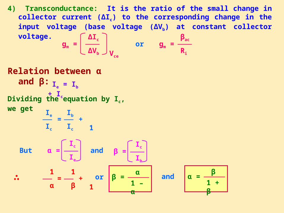
4) Transconductance: It is the ratio of the small change in collector current (ΔIc) to the corresponding change in the input voltage (base voltage (ΔVb) at constant collector voltage.
gm = ΔIc
ΔVb Vce
or gm = βac
Ri
Relation between α and β:
Ie = Ib + Ic
Dividing the equation by Ic, we get
= Ie
Ic
+ 1 Ib
Ic
α = Ic
Ie
β = Ic
Ib
But and
= 1
α+ 1
1
βor β =
α
1 – α and α =
β
1 + β
●
●
CL
●
Ece
●
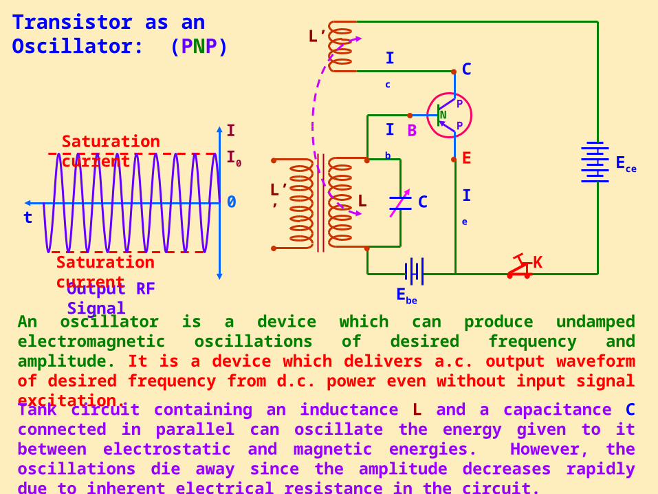
L’Transistor as an Oscillator: (PNP)
Ebe
Ic
E
B
C
P
PN
●●
●●
●
K
L’’
Ib
Ie
Output RF Signal
An oscillator is a device which can produce undamped electromagnetic oscillations of desired frequency and amplitude. It is a device which delivers a.c. output waveform of desired frequency from d.c. power even without input signal excitation.
I
I0
t0
Saturation current
Saturation current
Tank circuit containing an inductance L and a capacitance C connected in parallel can oscillate the energy given to it between electrostatic and magnetic energies. However, the oscillations die away since the amplitude decreases rapidly due to inherent electrical resistance in the circuit.
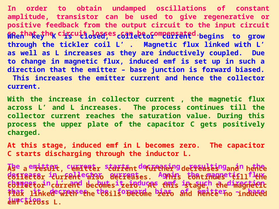
In order to obtain undamped oscillations of constant amplitude, transistor can be used to give regenerative or positive feedback from the output circuit to the input circuit so that the circuit losses can be compensated.
When key K is closed, collector current begins to grow through the tickler coil L’ . Magnetic flux linked with L’ as well as L increases as they are inductively coupled. Due to change in magnetic flux, induced emf is set up in such a direction that the emitter – base junction is forward biased. This increases the emitter current and hence the collector current.
With the increase in collector current , the magnetic flux across L’ and L increases. The process continues till the collector current reaches the saturation value. During this process the upper plate of the capacitor C gets positively charged.
At this stage, induced emf in L becomes zero. The capacitor C starts discharging through the inductor L.
The emitter current starts decreasing resulting in the decrease in collector current. Again the magnetic flux changes in L’ and L but it induces emf in such a direction that it decreases the forward bias of emitter – base junction.
As a result, emitter current further decreases and hence collector current also decreases. This continues till the collector current becomes zero. At this stage, the magnetic flux linked with the coils become zero and hence no induced emf across L.
2π
1f =
LC
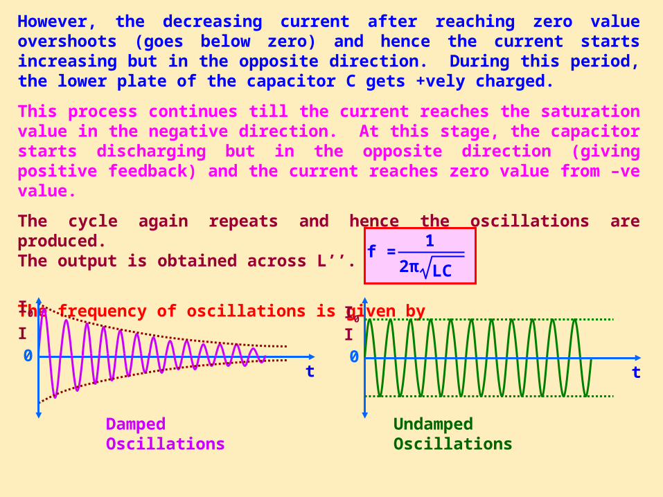
However, the decreasing current after reaching zero value overshoots (goes below zero) and hence the current starts increasing but in the opposite direction. During this period, the lower plate of the capacitor C gets +vely charged.
This process continues till the current reaches the saturation value in the negative direction. At this stage, the capacitor starts discharging but in the opposite direction (giving positive feedback) and the current reaches zero value from –ve value.
The cycle again repeats and hence the oscillations are produced. The output is obtained across L’’.
The frequency of oscillations is given by
II0
Undamped Oscillations
t0
I
I0
Damped Oscillations
t0