Switched-current logic for digital circuit design
55
AN ABSTRACT OF THE THESIS OF Vivek Subramanian for the degree of Master of Science in Electrical and Computer Engineering presented on February 1, 1991. Title: Switched-Current Logic for Digital Circuit Design Abstract approved: Redacted for privacy David J. Allstot A current-mode concept for digital integrated circuit design is introduced and is called Switched-Current (SI) Logic. This concept enhances high-performance mixed- mode IC design by reducing power supply noise spikes. The speed of operation is comparable with static CMOS logic gates. The basic building blocks of digital design are developed and categorized. The operation of these gates, the sources of noise spikes, concepts of noise margin and gate propagation delay are some of the aspects that are investigated. To test the practicality of this method representative digital circuits including a carry look-ahead adder are designed and fabricated in a 2-gm p-well CMOS process. Simulation results show that this technique reduces the associated power supply noise spikes by approximately two orders in comparison to standard static CMOS logic. The power supply noise spikes were measured to be about 15 pA with a gate delay 0.6 ns for a bias current I = 100 IAA.
Transcript of Switched-current logic for digital circuit design

AN ABSTRACT OF THE THESIS OF
Vivek Subramanian for the degree of Master of Science in Electrical and Computer
Engineering presented on February 1, 1991.
Title: Switched-Current Logic for Digital Circuit Design
Abstract approved:Redacted for privacy
David J. Allstot
A current-mode concept for digital integrated circuit design is introduced and is
called Switched-Current (SI) Logic. This concept enhances high-performance mixed-
mode IC design by reducing power supply noise spikes. The speed of operation is
comparable with static CMOS logic gates.
The basic building blocks of digital design are developed and categorized. The
operation of these gates, the sources of noise spikes, concepts of noise margin and gate
propagation delay are some of the aspects that are investigated. To test the practicality of
this method representative digital circuits including a carry look-ahead adder are
designed and fabricated in a 2-gm p-well CMOS process. Simulation results show that
this technique reduces the associated power supply noise spikes by approximately two
orders in comparison to standard static CMOS logic. The power supply noise spikes
were measured to be about 15 pA with a gate delay 0.6 ns for a bias current I = 100 IAA.

Switched-Current Logic for Digital Circuit Design
by
Vivek Subramanian
A THESIS
submitted to
Oregon State University
in partial fulfillment ofthe requirements for the
degree of
Master of Science
Completed February 1, 1991
Commencement June, 1991

APPROVED:
Redacted for privacyProfessor of Electrical and Computer Engineering in charge of major
Redacted for privacyHead of the Department of Electrical and Computer Engineering
Redacted for privacy
Dean of Graduate'Sdhoo1
Date thesis is presented February 1. 1991
Typed by researcher for Vivek Subramanian

ACKNOWLEDGEMENTS
I would like to thank my major professor and " God Father", Dr. D. J. Allstot
for all the encouragement and guidance throughout this entire project. His vast
experience and knowledge added to his gift as a teacher made learning a pleasure. I
must also thank him for helping me financially and giving me different perspectives to
life.
I would also like to acknowledge the help of Guojin Liang for introducing me to
this topic and for all the helpful hints and suggestions at times of despair; my colleagues
Terri Fiez, Ayse Yesilyurt, San-Hwa Chee, Paul Lao and Sailesh Maskai for their help
and hours of interesting discussions. I thank Dr. Goodnick, Dr. Roy Rathja and Dr.
Juha Pohjapelto, the members of my graduate committee for their time and effort during
my stay at O.S.U; Rita, Cindy and Susy from the ECE head quarters, for giving me the
strength to hang in there and for a friendly word each morning.
Further, I would like thank my personal friends, Ashok Ramchandran, without
whom life here would have uninteresting, for his thoughtfulness and his professorial
classes; Sudhir and Priti Agarwal who kept the doors of their house ever open to me;
Patrick Rochelle and Farroh Seifkhani for keeping my spirits HIGH; my friends at
Oregon State University for all the good times.
Most importantly, I am grateful to my family Mrs and Mr Subramanian,
Sanjeev, Archana and Raghu, for without them there would be no me. Their total faith
in me gave me the sense of confidence that I needed. Life in the U.S. would not have
been easy if not for their love and affection and their constant encouragement. I must
also thank my aunt and uncle, Romola and Darwin Thorbeck, for all their love showered
upon their "adopted son" and for providing me a home away from home. I dedicate this
thesis to my family.

TABLE OF CONTENTS
1. INTRODUCTION 1
2. THE SWITCHED-CURRENT (SI) LOGIC 4
2.1 A Current Mirror 4
2.2 The SI Logic Inverter 6
2.3 The SI Logic NOR 9
2.4 The Input V-I and Output I-V Translators 11
2.4.1 The Input Voltage-to-Current Converter 11
2.4.2 The Output Current-to-Voltage Converter 12
2.5 Input/Output Buffers 13
3. PERFORMANCE ANALYSIS OF SI LOGIC CIRCUITS 15
3.1 Power Supply Noise Spikes 15
3.2 Noise Margin 22
3.3 Speed Characteristics 25
3.4 Power-Delay Product 29
4. DESIGN OF DIGITAL CIRCUITS 30
4.1 Ring Oscillator 30
4.2 A 4-Bit Carry Look-Ahead Adder 36
4.3 Sequential Circuits 40
5. SCALING OF TECHNOLOGIES 41
5.1 The Scaling Laws 41
5.2 SI Logic under the CE and CV Scaling Laws 42
6. CONCLUSIONS 44
REFERENCES 45

LIST OF FIGURES
Figure Eau2.1 A simple current mirror 5
2.2 Transfer characteristics of a current mirror, L1 = L2 6
2.3 A switched-current (SI) inverter 7
2.4 The simulated input and output waveforms of a SI inverter for I = 100 I.LA 8
2.5 A practical implementation of a SI inverter with fanout = 2 9
2.6 A two-input SI logic NOR gate with fanout = 1 10
2.7 A simple input voltage-to-current translator 12
2.8 A simple output current-to-voltage translator 13
2.9 A tapered buffer design to reduce the loading effect of pin capacitance 14
3.1 A static CMOS inverter in p-well technology 16
3.2 A top view of the basic layout of a mixed-mode IC 17
3.3 Circuit to analyze the sources of noise generation in SI logic 19
3.3.b A SI inverter with PMOS cascode current source 20
3.4 The simulated noise spikes of both ground and power supply for I=100 µA 21
3.5 Voltage transfer characteristic of a static CMOS inverter 22
3.6 The transfer characteristics of a normal SI inverter 23
3.7 A practical SI inverter with enhanced noise margin 24
3.8 The transfer characteristics of a SI inverter with current gain = 1.5 25
3.9 Definition of delay characteristics of a SI inverter 26
4.1 Schematic of a 49-stage ring oscillator 31
4.2 The micro-chip photograph of three 49-stage ring oscillators with fanouts
of 1, 3 and 5 (left to right) for each inverter 32

Figure Page
4.3 The simulated output waveforms of a 49-stage SI ring oscillator with
fanout =1 for I =100 µA 32
4.4 Simulated variations in gate delay with change in bias current and supply
voltage with fanout =1 33
4.5 The power-delay curve of an SI inverter 34
4.6 The measured power supply and ground spikes of an SI inverter for
I = 100 RA and Vdd = 5 V 35
4.7 A block diagram of a 4-bit carry look-ahead adder 36
4.8 The output waveform of the 4-bit carry look-ahead adder 38
4.9 The micro-chip photograph of a 4-bit SI carry look-ahead adder 39
4.10 The schematic of a SI RS flip-flop 40

LIST OF TABLES
Table Page
2.1 Truth table of an SI current-mode inverter 6
2.2 Truth table of a two-input SI logic NOR gate 11
2.3 Truth table for an input voltage-to-current translator 12
2.4 Truth table for an output current-to-voltage translator 13
4.1 Simulated gate delay (ns) of an inverter with variations in power
supply and bias current for fanout = 1 31
5.1 The effect on transistor properties due to the basic scaling laws 42
5.2 Scaling of SI under constant field and constant voltage scaling laws 43

Kn
Kp
L
W
V
CX X
V XX
VT
k
8
I
LIST OF SYMBOLS
Transconductance of NMOS, p.A/V
Transconductance of PMOS, i.tA/V
Lenth of MOSFET, g
Width of MOSFET, p,
Voltage, volts
Capacitance in fFarad
Voltage of MOSFET, volts, where x= d = drains = sourceg = gateb = bulk
Threshold voltage, volts
Channel-length modulation, volts
exclusive-OR
Current, A

SWITCHED-CURRENT LOGIC FOR DIGITAL CIRCUIT DESIGN
1. INTRODUCTION
With the improvements in Integrated Circuit (IC) fabrication technology, the
integration of electronic circuitry has increased dramatically. A chip that once contained
a few hundred transistors may now contain as many as a million or more transistors,
with prospects for a billion transistors at the beginning of the next millennium.
In the beginning of this era of Large Scale Integration in the 1960's, the
emphasis was on bipolar analog integrated circuits. After the invention of the
microprocessor in the late 1970's, there was an explosion of interest in digital IC's
fabricated in Metal Oxide Semiconductor (MOS) technology. In recent years, mixed-
mode IC's containing both analog and digital circuitry have emerged for system
integration applications. Interestingly, technology has also advanced to incorporate both
bipolar and MOS capabilities, i.e. BiCMOS technologies.
Advancements have also occurred in the scaling of technologies and the
shrinking of the minimum sizes of transistors, accompanied by higher performance
processing parameters, reduction in power supply voltages, etc. [1]. These technology
changes have necessitated new analog and digital design techniques. For example,
noise spikes generated by the switching of MOSFET's in conventional static CMOS
digital circuits are propagated to the analog side in a mixed-mode IC and may degrade
the performance of the analog circuitry [2]. Due to this noise, there is presently an
upper limit on the accuracy of mixed-mode integrated systems.
As mentioned earlier, the advances in IC technology allowing mixed-mode
systems have created a need for new logic families that significantly reduce the power

2
supply noise generation of conventional CMOS static voltage-mode circuits [3].
Though static CMOS logic offers high performance with low static power, high
functional manufacturing yield and easy scalability to smaller device sizes, it typically
generates power supply noise spikes as large as 1 mA/gate. On a chip where many
thousands of transistors may switch synchronously, very large spikes may occur.
To circumvent the problem of noise propagation in mixed-mode IC's, several
techniques have been developed. Good layout techniques such as using separate analog
and digital power supply lines and minimizing their common impedances are somewhat
effective. The use of diffused guard rings to shield noise from analog circuitry is also
beneficial.
Statistics show that digital MOS IC's currently dominate and will continue to
dominate the IC market. Previously, the of operation of static CMOS logic circuits has
been in the voltage-mode domain. In this thesis, digital circuits that work in the current
domain are presented. A new concept for digital circuit design is introduced called
Switched-Current (SI) Logic. The traditional voltage levels for digital logic high or "1"
and logic low or "0", are replaced by current levels. The gates operate with a constant
current source and hence there are ideally no noise spikes generated. This SI logic
technique increases the performance of digital circuits over those that are voltage
controlled. The technique is especially intended for high performance mixed-mode
applications.
In chapter 2 the basic building blocks of this new logic family, the SI
INVERTER and the SI NOR gate are introduced. This chapter also deals with the
issues of maximum fanout and input/output buffers. The translators that convert from
voltage to current and vice versa are necessary to make SI compatible to the existing
CMOS logic families. Chapter 3 discusses the characteristics of the logic gates

3
including propagation gate delays, maximum speed and power supply noise spikes.
Chapter 4 considers the practical implementation of SI logic in both combinational and
sequential digital circuits. Several new SI circuit blocks are described and fabricated. In
order to predict the viability of SI for the future, Chapter 5 considers the performance of
SI with scaled CMOS technologies using two standard scaling laws - constant voltage
(CV) and constant electric field (CE).

4
2. THE SWITCHED-CURRENT (SI) LOGIC
On-chip digital logic levels have been traditionally defined by voltages. Using a
positive logic convention, a high voltage denotes a logic high or "1" and a low voltage
denotes a logic low or "0". In the switched-current (SI) technique, the logic levels are
defined in terms of currents and are ideally independent of the voltage levels. Thus, if a
branch has a high flow of current, it is termed as IH or a logic "in state, and if it has a
low flow of current, it is called IL or the logic "0" state.
2.1 A Current Mirror
Before considering the SI logic circuits, the simple current mirror is first
reviewed as it is an essential building block of this logic technique. The concept of
current mirroring is as literal as its name. Designers of bipolar and CMOS analog and
digital circuits often make use of this essential technique.
The basic idea is to replicate the current flowing in a particular branch to other
branches in a circuit. Figure 2.1 shows an NMOS implementation of a simple current
mirror. M1 is diode-connected and operates in the square-law saturation region when
biased with a current
resulting in [4]
VGS
The gate of M2 is driven
I =2
I
= VT1
as shown. Ml performs a current-to-voltage conversion on I
(2.1)
(2.2)
+ 21Kri(W/L)i
by VGS resulting in a current of
1A-71 - V 12GS T2)2
if M2 is in saturation for VDS2 > (VGS VT2) and a current of

12. = L1
1
-V 1V IV2DS2IGS T2) DS2 I 2
5
(2.3)
if M2 is in non-saturation VDS2 < (VGS VT2). The output I-V characteristic of the
simple current mirror obtained from (2.2) and (2.3) is shown in Fig. 2.2. Assuming
that L1 = L2 and Ml and M2 are both saturated,
I =I2-W2 W1
) (2.4)
By varying the ratio of the widths of the transistors, the desired current can be generated
with respect to the bias current I flowing into Ml.
Vdd
M1
VGS
Figure 2.1 A simple current mirror.

6
(W2) I(W1)
VGs2 = VGS1 VG s
Non-S aturationi Saturation
VGS - VT2 VDS2
Figure 2.2 Transfer characteristics of a current mirror; L1 =1-2.
2.2 The SI Logic Inverter
The inverter is the basic building block for all digital circuits. Figure 2.3 shows
a schematic of an SI inverter consisting of Ml, M2 and M3 with the corresponding
current-mode truth table given in Table 2.1. Recall that IH represents a logic "1" and IL a
logic "0" and that M3 realizes the constant current source I. Simulated input and output
current waveforms are shown in Fig. 2.4, for the SI inverter of Fig. 2.3 assumed
driving the input of an identical stage.
INPUTI Evi
OUTPUTIola
IH IL
IL 1H
Table 2.1 Truth table of an SI current-mode inverter.

7
At t=0, IIN = IH and Ml and M2 are both conducting. Hence IouT = IL = 0 flows into
the diode-connected input of the next stage. When IJN(t) changes to IL, both Ml and M2
turn off and the output current flowing into the input of the next stage increases to IH = I
as shown in Fig. 2.4. Note that IH is slightly less than I due to channel-length
modulation effects of the PMOS current source. If necessary, this effect can be
eliminated by replacing M3 by a cascode PMOS current source. A 2-p.m p-well CMOS
process parameters were used for all the simulation results presented in this thesis.
As mentioned earlier, mirroring produces equal currents if the transistors are
identical including their voltages, K factors and dimensions W and L. In practice this
does not occur and hence M2 must be made bigger than Ml to achieve current gain to
compensate for possible errors, and to provide a sufficient noise margin.
ii4 (4/2)1 : 1.5
Vdd
I (8/2)
M3OUT
(6/2) 1,
Ml M2
Figure 2.3 A switched-current (SI) inverter.

0.1/5
0.15
0.125
0.1E
0.075wQcc 0.05ca
0.025
0.0
SI INVERTER WAVEFORMS for I-100 uA
IOUT(t) 1'0)r
..
...
*
---**
25 50TIME (ns)
75
Figure 2.4 The simulated input and output waveforms of a SI inverter for I = 100
co

vdd
MO
Ml 1 : 1.5
OUT1
1 : 1
OUT2
H
Figure 2.5 A practical implementation of a SI inverter with fanout = 2.
9
MS
M4
The current sources shown in Fig. 2.5 are implemented using simple PMOS and
NMOS current mirrors. The circuit shown is a practical realization of a SI inverter with
fanout of two. Unlike static CMOS logic or other voltage-mode circuits where multiple
fanouts are driven from the same point, an extra output stage (represented by transistors
M4 and M5 ) is required for each additional fanout with current-mode SI logic. loun =
Isom is obtained when
L L 1,.f Al and 1 3Y1 .11AL1
4 L)2 (2.5)
2.3 The SI Logic NOR
The SI NOR gate is an extension of the SI inverter. Figure 2.6 illustrates the
schematic of a two input NOR gate with a fanout capability of one. The operation of

10
this circuit is similar to that of the SI inverter just discussed. When the inputs NI and
11/.12 are both high, pushing currents IH = I into M1 and M5 respectfully, then M1, M2,
M4 and M5 all turn on. Hence, the bias current I splits evenly between M2 and M4.
Thus, the output current is designed to be zero to ensure that the subsequent stage is
turned off. If there are "n" input NOR stages and all of them turn on, then the bias
current splits into I/n. In the worst case, the circuit is designed so that even if only one
input is high then the output current is still zero. Only when all the inputs are low do all
of the transistors turn off allowing the output to attain the high level, IH. An arbitrary
number of inputs can be added to the NOR gate, although as mentioned before, each
fanout requires an additional output branch.
IIN1
Vdd
M6
II
OUT
1:1.5 M2 M4 1.5:1 M5
Figure 2.6 A two-input SI logic NOR gate with fanout = 1.

11
I IN1 1 1112 LOUT
IL 1
LI
H
ILIII
IL
IH 111 II,
IH I IL
L
Table 2.2 Truth table of a two-input SI logic NOR gate.
Table 2.2 gives the truth table of a two-input SI logic NOR gate. A suitable technique
for realizing NAND gates with SI logic has not yet been found, although it is not needed
as a NOR gate is a logically complete set.
2.4 The Input V-I and Output I-V Translators
The current-steering logic circuits discussed so far are intended strictly for on-
chip applications as they have their inputs and outputs in terms of currents. In practice,
these circuits interface to existing logic families such as CMOS static logic, and thus
there is a need for converting from current-to-voltage and vice-versa.
2.4.1 The Input Voltage-to-Current Converter
Figure 2.7 shows the schematic of a simple input V-I converter. When the input
VIN is less than VT1, Ml is off and the current available at the output to flow into the
next stage is I. Similarly when VIN > VTi(e.g., VIN = Vdd), then Ml is on and designed
so that all of the bias current I flows to ground, and 'our = 0. The truth table for the V-I

12
translator is shown in Table 2.3.
VIN
Vdd
0
Figure 2.7 A simple input voltage-to-current translator.
INPUTVIN
OUTPUTTOUT
VIH IL
V113 IH
Table 2.3 Truth table for an input voltage-to-current translator.
2.4.2 The Output Current-to-Voltage Converter
Figure 2.8 shows the schematic of one possible simple output I-V converter.
M3 is biased with a multiple of I similar to a standard SI inverter. When 'IN = IL, M2 is
turned off, and M3 charges the output capacitive load, CL, to the power supply voltage.
When 'IN = IH, Ml and M2 are on, and M2 and M3 are properly ratioed so that the
voltage at the output node is low, VoL. The truth table is shown in Table 2.4.

13
IIN
VBIAs
M1
Vdd
M3
M2
Figure 2.8 A simple output current-to-voltage translator.
INPUT
Inv
OUTPUT
VOUT
IH VOL
IL VDD
Table 2.4 Truth table for an output current-to-voltage translator.
2.5 Input/Output Buffers
The input and output variables of SI logic are current signals. In a practical IC
design, the voltage outputs of the on-chip gates are connected to IC package pins loaded
with large capacitances greater than 10-15 pF. The output stage with such external
loading often limits the speed of the overall circuit. Hence, practical output buffers are
used which are a series of tapered CMOS gates cascaded together. Size tapering is done
to reduce the loading effect of the pin capacitance and to minimize the total load driven
by the internal gates. From practical experience, it appears best to include an I-V

14
translator preceding the tapered buffer to ensure a full logic voltage swing at the output
as shown in Fig. 2.9.
E-4
To pinof IC
Cg
Figure 2.9 A tapered buffer design to reduce the loading effect of pin capacitance.
The buffer is designed by using the following approach. Denote the gate capacitance of
the minimum sized inverter as CG and the load capacitance as CL. Now
let
and
y = / CG
y =fN
(2.6)
(2.7)
where N = number of stages and f = e = 2.313 is the optimum upscale factor [5].
Starting with the minimum sized inverter, the (W/L) ratios of the subsequent stages are
scaled up by multiplicative factors off as shown in Fig. 2.9.

15
3. PERFORMANCE ANALYSIS OF SI LOGIC CIRCUITS
In this chapter, the power supply noise spike generation and speed
characteristics of SI logic gates are considered. It is shown that SI logic has a
significant advantage over conventional static CMOS logic families in terms of power
supply noise generation. This key advantage may be especially important in high-
performance mixed-mode applications.
3.1 Power Supply Noise Spikes
Power supply noise is an unwanted signal in the form of a voltage or current that
causes deviations from ideal behavior. Noise can originate at the inputs or be generated
in the power supply or in the ground lines due to the switching of logic gates.
With the increasing emphasis on combining high-performance analog with high
speed digital circuits on the same chip, and with experience that the accuracy of such
analog circuits is currently limited by power supply noise, considerable work is going
into reducing or eliminating power supply noise. The SI logic technique reduces power
supply noise by nearly two orders of magnitude.
In conventional CMOS digital circuits, overlap current pulses are caused by the
switching of transistors, and result in power supply and ground noise. Consider the
case in static CMOS circuits where the power supply noise spike from a gate could
measure as large as 1 mA. On an integrated chip with many thousands of transistors
which may be switching synchronously, the total power supply noise spike may be very
large. When this happens, the analog circuitry sees this as power supply noise which
degrades its performance [6].

GND VDD
16
P-WELL
N SUBSTRATE
Figure 3.1 A static CMOS inverter in p-well technology.
Figure 3.1 shows a cross-sectional view of a static CMOS inverter. Note that
the implementation is in a p-well CMOS technology and hence there is sharing of the
common N-type substrate between the analog and digital circuitry. To ensure that latch-
up does not occur, the digital power supply Vdd is locally tied to the substrate within
each of the digital cells, and the p-wells are connected to ground. Hence, noise
generated on the digital power supply (Vdd) lines is directly coupled into and propagated
throughout the N-substrate.

VDD
ANALOGCIRCUIT
BONDING WIRE
V ±
DIGITALCIRCUIT
'SPIKE
R + L
Figure 3.2 A top view of the basic layout of a mixed-mode IC.
Figure 3.2 shows a top view of the layout of a typical mixed-mode chip. The power
17
supply noise due to a power supply current spike, IsPIKE, is given by
SPIKENOISE SPIKE
Ldt (3.1)
Noise spikes directly affect the accuracy of the analog circuitry because the noise is
coupled to the analog from the digital part due to the common power supply impedance
and the common substrate. The common power supply impedance is minimized by
using separate on-chip analog and digital power supply and ground lines and pins.
The main advantage of SI logic is that by using constant current sources, the
power supply current is ideally constant and theoretically there is no power supply
noise. The non-ideal sources of noise generation are now analyzed. Figure 3.3 shows
a pair of SI logic inverters. M3 operates in the saturation region and the current flowing
through it is given by

K 1
II1H- V + W2 A L SG3 T3
18
(3.2)
The voltage change at the output node which results in a change in current flowing
through M3 is about 1V. Due to the channel-modulation effect the change in current 13
with respect to Vds3 is given byK 1(DI
3 = 11H-- RTSG3 + VT3 )aysd3 2 ) L (3.3)
which is represented as I (X, AV). This is the square wave part of the measured power
supply noise in Fig. 4.6.
The power supply noise is also caused by the displacement current. The change
in the output voltage due to the turn-on and turn-off of diode M4 causes the supply
capacitance Cdd to charge and discharge. Cdd is the capacitance between the power
supply and the output node as shown in Fig. 3.3. The change in the output voltage is
given bydV Idt Cror (3.4)
where CTOT is the total capacitance at the output node equal to Cdb2 + Cgd2 + Cdb3 +
Cgd3 Cgb4 Cdb4 Cgs4 Cgs5 Cgb5 Cgd5. The power supply displacement
current is then given bydV=c
dd dd dt dd CitiT (3.5)
where neglecting interconnect capacitances, Cdd = Cdb3. This is the spike that is seen the
in the measured power supply noise in Fig. 4.6.
In a similar way the gate capacitors in M1 and M2 are also charged and
discharged to generate noise that in this case flows into ground. This noise spike is
given by

19
dVIGND
= (Cdb2 Cgs4 +Cgb4 +C +C
gs5 + Cgb5 J dt (3.6)
where the dominant capacitances, Cgsi and Cgs2 are the gate capacitances of M1 and
M2. Thus,
(C + IGND gs 1 Cgs2) clur (3.7)
The ground spike is typically larger than the Vdd power supply spike. However, in a p-
well CMOS technology, the wells are isolated from the substrate which is common to
the analog circuitry and hence, ground noise does not affect the performance of the
analog circuit provided separate analog and digital ground lines are used. It is also
assumed that the preceding stage is turned off instantly which is not the case. Hence all
the current does not flow immediately into the input node and charge up the
capacitances. The result of a simulation for a bias current of 100 1.1A is shown in Fig.
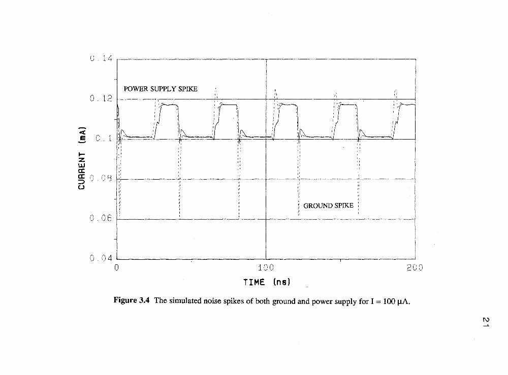
3.4. From the graph it can be seen that the power supply spike is about 15 1.tA.
Compare this to the 1 mA spike that is obtained from switching a CMOS inverter and a
reduction in magnitude by a factor of 70 is achieved. The ground spike is found to be
about 40 I.LA.
vdd
M1 1: 1.5
CTOT
(---- I
TOUT
11111 M2 M4 1 : 1.5 M5
M6
I
Figure 3.3 Circuit to analyze the sources of noise generation in SI logic.

20
Vim.
VIN2
I
vdd
M3A
1 : 1.5
....4M6A
M6
OP
IOUriM5
Figure 3.3.b A SI inverter with PMOS cascode current sources.
U. 14
0.12
E
wCC
CC 0.08
0.06
0.04
POWER SUPPLY SPIKE
,
GROUND SPIKEi
0 100
TIME (ns)200
Figure 3.4 The simulated noise spikes of both ground and power supply for I = 100 RA.

22
3.2 Noise Margin
Large noise signals cause logic errors. However, if the noise amplitude at the
input of any logic circuit is smaller than a specified magnitude known as the "noise
margin", it is attenuated. Noise margins are defined as the ranges between which the
circuit does not mistake noise for a valid input signal; they are important properties of
any logic circuit. Due to their regenerative nature, noise in digital circuits does not
accumulate from one stage to the next which is a distinct advantage over analog [7]. The
transfer characteristic of a voltage driven static CMOS inverter is shown in Fig. 3.5.
Figure 3.5 Voltage transfer characteristic of a static CMOS inverter.
The static noise margins are defined by
NMH = VOH Vg; which is the logic-high noise margin, and
VOL which is the logic-low noise margin.

23
The static transfer characteristic of a SI inverter with current gain = 1 is shown in Fig.
3.6. The inverter has zero NMH and NML noise margins, and is therefore impractical.
Figure 3.6 The transfer characteristics of a normal SI inverter.
To design a practical SI inverter as in Fig. 3.7, a current gain greater than one
(typically 1.5 to 2.0) is needed. This multiplicative factor is called the Shape Factor.
The current gain is achieved by increasing the width of the mirroring transistor M2 by
the shape factor. Referering to Fig. 3.7, the shape factor ratio of the inverter with gain
G is
(W/L)2G=),
= 1.5 K(W/L)1 (3.8)
The interpretation of the noise margin in this case is analogous to the CMOS inverter
discussed above. Thus the logic-high noise margin is NMH = I0H - IN and the logic-low
noise margin NML = IIL Ism where the quantities are defined in Fig. 3.8. From
Fig. 3.8 the input logic levels are shown to be Ill, = 0 and Im = 0.671 and the output

24
logic levels are 'OH = I and the 10L, = - 0.51. Thus the NMH = 0.331 and the NML, =
0.51. With a shape factor of two the logic-low and logic-high noise margins are equal.
To analyze the circuit in Fig. 3.7 to show that is has enhanced noise rejection
capability, let the input current change from a logic low level to a high level. The bias
current I flows through M1 and establishes a voltage, VGS1. As M1 and M2 share the
same gate, VGsi = VGS2 Since (W/L)2 = 1.5 (W/L)1, a current 1.51 flows through M2
(assuming M2 operates in saturation). On the other hand, the total current available to
M2 is only I. M1 operates in saturation and so would M2 if the required current 1.51
was supplied. But since only I is supplied to M2, it operates in the non-saturation
region. This ensures that Vds2 < VT and that the next stage is turned off.
Now let the inverter in Fig. 3.7 be driven by an identical stage. M1 is off if the
input current is zero. The driving transistor of the previous stage is capable of sinking
1.51. Thus, even if there is an error in the input current as large as 0.51, it is sunk into
the previous stage and M1 remains turned off.
I1
1
Vgsl 1: 1.5
Vdd
iM3
I
m2
LOUT
Figure 3.7 A practical SI inverter with enhanced noise margin.

Tin
25
Figure 3.8 The transfer characteristic of a SI inverter with current gain = 1.5.
3.3 Speed Characteristics
Another significant aspect of the SI logic family is its speed of operation. Input
and output current waveforms for an SI inverter are shown in Fig. 3.9. The levels of
operation are IH and IL. The region between these two levels is the transition region.
The triggering of an SI logic gate is hence based on a threshold parameter IT, defined as
the minimum current needed to turn it ON. It is defined as the 50 percent point of the
transition region. The delays of the inverter are measured between the IT point of the
input and the corresponding output. Simulation results show that the delay is as low as
0.3 ns for I = 300 j.tA and (W/L)i = (31.1/211), (W/L)2 = (6p./2[t) in a 2 gm p-well CMOS
technology.
The delays are determined by analyzing the switching of the three transistors
M1, M2 and M3 of the inverter in Fig. 3.7. Transistor Ml is the input transistor while

26
the other two are the output devices Ml is diode-connected and operates in either the
cutoff or saturation region. The delay involved in switching the SI inverter is analyzed
in terms of its rise and fall time. The time required to charge the input capacitance in
addition with the time to turn on Ml and M2 (discharge the output node) is the rise time,
TR. The time required to both turn off Ml and M2 (charge the output node) and
discharge the input capacitance is the fall time, TF. When the input is IL, Ml is off and
the output is IH. The input is next changed to Ill. With I< IT, Ml is off and capacitors
Cin + + C + CCdbl+ Cgbl Cgsl -gb2 -gat Cgd2 are charged by M3.
'in
TF
Figure 3.9 Definition of delay characteristics of a SI inverter.

dVgs1IH = C
dt
T1 = CAV
°-
27
(3.9)
(3.10)
where T1 is defined as the time needed to charge the input capacitors.
When VGs > VT, Ml and M2 turn on, and the output starts to fall towards IL.
The current available to charge the input capacitance is now lc and is given by
IC = IH
CinT2
(V -Ki GS11V 12 Vgs
CinAV
Cin where (3.11)
(3.12)
T1) =dt
(
T2
Cj2 11 1n
2 KiI
is the time needed to turn on M2. The total rise time TR is given by T1 + T2.
Now when the input changes to IL, M2 turns off, and then M1 turns off and Cin
discharges through the input node of diode M1 to the previous stage. The time taken for
this is TF. The charging current is the same as when Cin was being charged, but in the
opposite direction. Hence,
and
dVgslI = I + K IV V 2 CC L GS1 T11) -Cinin dt
TF = Cin 1, tan-1
K1
K, K, )I IK2 - K1
I
(3.13)
(3.14)

28
The propagation delay time Tdelay is defined as (TR + TF)/2 and given as
\C. AV , C. v K2 + V KiT g m i 1 in
delay 2 1H
4 K II IX liTS
( li KiC.
2m i11( - K 1 I tan-1
2 1 j K2 K11 (3.15)
The reasons for high speed of operation of the switched-current inverter are seen by
examining the charging current given by
Or
I =C dVdt
t = CAI where t is the delay time. (3.16)
The voltage swing in SI logic is very small, about 500 mV as compared to 5 V for
conventional static CMOS logic. Thus, from (3.16), the SI logic gate is potentially very
fast. Minimum dimension inverters are used with (W/L) values of (3g/211). By
reducing the size of the transistor, the capacitance become smaller. Also note that a
constant current is charging a diode-connected transistor. By increasing the current, the
delay of the SI logic gates is reduced.

29
3.4 Power-Delay Product
From the delay time calculations (3.15) the power-delay product (PDP) is determined as
PDP = Vdd I Td
rVddCiriAVgs VddCm. .s/ K2 + Kir-1
+
IIn
2 4 Ki K2 - K1 l
2tai Ki
K2 - K1 K2 K1V Cdd i n-n Ni
(3.17)
The power-delay curve is shown in Fig. 4.5. As the current is increased, the time
needed to charge the capacitance decreases and hence the gate delay is reduced. But, as
the bias current is increased the size of the transistors have to be increased so as to
maintain a proper logic swing. With the increase in transistor sizes, the parasitic
capacitances also increase. Hence there is a limit to which the current can be increased.
Depending on the limit of power dissipation, the bias current is chosen thereby setting
the gate delay.

30
4. DESIGN OF DIGITAL CIRCUITS
Having seen that SI logic gates function as predicted, several basic digital
circuits are now implemented. Both combinational and sequential circuits are designed
and analyzed.
4.1 Ring Oscillator
A basic digital circuit to study power-delay performance is a ring oscillator. The
time period of oscillation is given by
T = n t, where n = number of stages (odd only) (4.1)
ti = delay of an inverter
T = Time period of oscillation
A ring oscillator is implemented as a series of inverters with the output of the
final stage connected to the input of the first stage. To limit the frequency of oscillation
below 50 MHz so that it could be easily measured, and assuming a gate delay of 1 to 2
ns per stage, a 49-stage ring oscillator was designed. To study fanout effects, three
circuits were designed and implemented with fanouts of 1, 3 and 5. The three ring
oscillators were then implemented in the 2 micron p-well process and fabricated by MOS
Integration Services (MOSIS). The schematic of the circuit is shown in Fig. 4.1 and a
microphotogrpah of the fabricated IC in Fig. 4.2.

For each inverter
(W/L)141,---411/2p, -NMOS
wi611/21.t -NMOSM3 =6µ /2µ -PMOS
Figure 4.1 Schematic of a 49-stage ring oscillator.
BIAS CURRENT
gA50 100 150 200 250 300 350
5.0 1.15 0.768 0.586 0.491 0.440 0.396 0.357
4.5 1.18 0.744 0.598 0.512 0.448 0.364 -4.0 1.24 0.788 0.630 0.512 -3.5 1.287 0.841 0.611
3.0 1.346 0.813 0.606 -2.5 1.557
31
Table 4.1 Simulated gate delay (ns) of an inverter with variations in power supply and
bias current for fanout = 1.

32
Figure 4.2 The micro-chip photograph of three 49-stage ring oscillators with fanouts
of 1, 3 and 5 (left to right) for each inverter.
6
4
-J02
0
T = 65 ns..
-20 100 20'0 300
TIME (45)
Figure 4.3 The simulated output waveforms of a 49-stage SI ring oscillator with
fanout = 1 for I = 1001.1A.

33
Figure 4.3 shows a simulated output waveform for the 49-stage ring oscillator
with a bias current of 100 .tA. The oscillation waveform is in terms of voltage as a
output I-V buffer was used. The ring oscillator in Fig. 4.1 was simulated with different
values of the bias current and the power supply voltages as shown in Table. 4.1; and the
simulated results are plotted in Figs. 4.4 and 4.5.
0 100 200Bias Current(uA)
300 400
Figure 4.4 Simulated variations in gate delay with change in bias current and supply
voltage with fanout = 1.
The graphs show that the delay of an SI inverter varies inversely to the bias current and
is approximately constant with power supply voltage. A specific bias current is selected
for a given speed requirement.

1."
0
.
NO
34
Power Delay Curve
0 1
Power (mW)
Figure 4.5 The power-delay curve of an SI inverter.
Figure 4.5 shows the simulated power-delay curves of an SI inverter; the delay
of an inverter decreases as the power consumption increases. The graph also shows that
the power-delay performance is insensitive to power supply variations. It is desired that
the power-delay product be minimized and this aspect is taken up later. The measured
power supply and ground spikes are shown in Fig. 4.6. The power supply noise spike
is measured to be 18 1.1A, in good agreement with the simulation results.

35
1111111111111111111111111111111
1111111111111111111111111111
!x_RPIGisgelnl!miliant11111111111111111111111111111
11111111111111111111111111111
2t.! s/di v
Power supply current spikes
11111
111
INW11111116_11;e1
1111111 111111111111
Flom- am21.1s/div
Ground current spikes
Figure 4.6 The measured power supply and ground noise spikes of an SI inverter
(fanout = 1) for I = 100 l_tA and Vdd = 5 V.
36
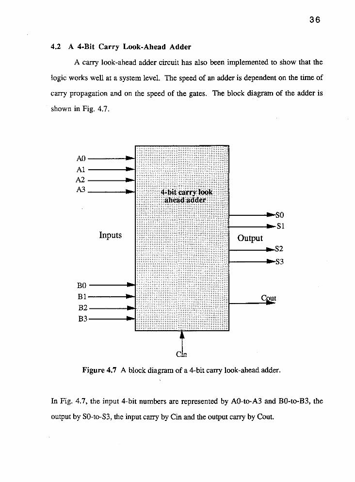
4.2 A 4-Bit Carry Look-Ahead Adder
A carry look-ahead adder circuit has also been implemented to show that the
logic works well at a system level. The speed of an adder is dependent on the time of
carry propagation and on the speed of the gates. The block diagram of the adder is
shown in Fig. 4.7.
AO
AlA2A3
BO
B1
B2
B3
No-
Inputs
4-bit carry lookahead adder
SO
S1
Output
lb. S3
Cout
Figure 4.7 A block diagram of a 4-bit carry look-ahead adder.
In Fig. 4.7, the input 4-bit numbers are represented by AO-to-A3 and BO-to-B3, the
output by SO-to-S3, the input carry by Cin and the output carry by Cout.

37
The logic equations of the adder [8] are given by the
SUM = AI 8 BI 0 CI where 8 is XOR (4.2)
CARRY = GI + PIGI-1 + P
IP
I-1GI-2 + + PIPI-1
P1GI-0 + PIPI-1 Co (4.3)
where PI = A/ + B/ (Propagate signal ) (4.4)
0/ = A/ x 13/ (Generate signal ) (4.5)
A carry is formed at the output of a given stage if one is generated in the given stage or
in a previous stage and propagated to the given stage. Figure 4.8 shows the simulation
results of the adder. The micro-chip photograph of the adder is shown in Fig. 4.9. The
simulations predict a power dissipation of 320 mW.

F-zcr. 0.075cc
(-3 0 05
0.15
0.125
0.1
0.025
0.0
INPUTS: AO Al A2 A3
1 1 0 1
B1 B2 B3 B4
0 1/0 1 0
ALL OUTPUTS(bits) IN CURRENTS
SUM1 -1'
COUTOUTPUT] 0
OUTPUT2 1
SUM4 SUM31 1
0 0
SUM2 5
1
1
i SUM2_____Io
,1
I
,\
,,
i
SUM31
1
SUM4 ' , i4 COUT\
/ \ i
._
0 50
TIME
75
Figure 4.8 The output waveform of the 4-bit carry look-ahead adder.
UM1
1

39
Figure 4.9 The micro-chip photograph of a 4-bit SI carry look-ahead adder.

40
4.3 Sequential Circuits
After looking at the functionality of combinational circuits, basic sequential
circuits were designed and simulated [9]. A simple RS flip-flop is shown in Fig. 4.10.
In a similar way, other sequential circuits are implemented. Because each fanout from a
SI logic circuit requires a separate output branch, circuits that are optimum in terms of
area/speed for conventional logic may not be optimum for SI implementations. This is a
topic for future study.
S
Figure 4.10 A schematic of a SI RS flip-flop.

41
5. SCALING OF TECHNOLOGIES
Continuing improvements in IC fabrication technology make it possible to
reduce the internal dimensions of semiconductor devices. Early IC technologies had
minimum dimensions of about 20 pm, while the present industry standard is sub-
micron. The circuits described in this thesis are implemented in a 2 p.m technology.
The trend to reduce device dimensions will likely continue until the fundamental physical
limitation of about 0.10 p.m is reached [10]. Another limitation is due to a mechanism
called subthreshold conduction [11]. It's effect is that the drain current does not go to
zero at Vgs = Vt, but instead falls exponentially with decreasing Vgs. Thus this puts a
limit on scaling the threshold voltages, especially in dynamic circuits in which the
current in the off state must be very small. Scaling is a way to reduce the power-delay
product of a device. The idea is to reduce the delay as well as the amount of power
dissipated, subject to other design constraints.
5.1 The Scaling Laws
There are at least three scaling laws that are used to determine the performance of
scaled circuits. They are the constant voltage (CV), the constant electric field (CE) and
the quasi constant voltage (QCV). QCV is used with the reduction of power supply
voltage from 5 V to 3.3 V. CV is the most widely scaling law used and will be used in
our analysis along with the CE law. Table 5.1 shows the effects of scaling on various
transistor parameters with respect to a scaling factor K, which is greater than 1.

42
TRANSISTORPROPERTIES CE QCV CV
Voltages(Vdd & Vt)
1/K INK 1
Lateral Dimension(W &L)
1/K 1/K 1/K
Vertical Dimension(X & Tox)
1/K 1/K 1/VK
Doping Concentration(ND) K K K
Table 5.1 The effect on transistor properties due to the basic scaling laws.

43
5.2 SI Logic under the CE and CV Scaling Laws
The SI logic circuits are analyzed using the relations in Table 5.1. The relations
of the various parameters and characteristics are tabulated in Table 5.2. From the
equations (3.10), (3.12), (3.14) (3.15) and (3.17), recall that the rise time TR = T1 +
T2, the fall time is TF and that Tdelay is the gate propagation delay.
TRANSISTORPROPERTIES CE CV
Capacitance 1/K INK
Transconductance K 'N/K
Rise time [ TF ] -rile T2/K31' T1 /K3/2 + T2/04
Fall time [ T F ] 1e2 i/K7/4
Bias Current [ I] 1 1
Power consumption 1/K 1
Table 5.2 Scaling of SI under constant field and constant voltage scaling laws.
Thus the performance of the SI logic circuits will improve with scaling and hence can be
used with future scaled industry standards.

44
6. CONCLUSIONS
A new logic family called switched-current logic (SI) was implemented. This
logic works in the current domain unlike the existing conventional static CMOS logic
families that work in the voltage domain. Using simple circuits, SI logic can be
interfaced with the existing CMOS families. The delay of the SI logic inverter was
simulated to be as low as 0.3 ns at I = 300 RA and Vdd = 5 volts; hence, the speed is
comparable to that of a static CMOS gate. The speed of the gates can be increased by
scaling the dimensions of the transistors. The propagation delay of the logic is found to
independent of the power supply voltage and depends only on the constant bias current.
The power supply noise spikes are measured to be 15 RA for an input current of 100 RA
in comparison to the power supply noise spike generated from a static CMOS inverter of
1 mA. Thus, one the limitations in mixed-mode IC design is nearly eliminated. Several
experimental SI logic IC's were fabricated in a 2 pm p-well CMOS technology available
from the MOSIS service.

45
REFERENCES
[1] S. Wong and C.A.T. Salama, "Impact of scaling on MOS analog performance,"
IEEE J. of Solid-State Circuits, vol. SC-18, no. 1, February 1983.
[2] J.A. Olmstead, "Noise problems in mixed analog-digital integrated circuits,"
Proc. of the IEEE Customs Integrated Circuits Conference, 1987, pp. 659-662.
[3] D.J. Allstot, S. Chee, S. Kiaei, "CMOS source-coupled logic for mixed-mode
VLSI," Proc. of IEEE International Symposium on Circuits and Systems, May 1990,
pp. 1608-1611.
[4] H. Shichman and D.A. Hodges, "Modeling and simulation of Insulated-Gate Field-
Effect Transistors," IEEE J. of Solid-State Circuits, vol. SC-3, no. 5, September 1968,
pp 285-289.
[5] M. Nemes, "Driving large capacitances in MOS LSI systems," IEEE. Journal of
Solid-State Circuits, vol. SC-19, no 1, February 1984.
[6] H.S. Lee, D. Hodges, P.R. Gray, "A self calibrating 15 bit CMOS A/D converter,"
IEEE Journal of Solid-State Circuits, vol. SC-19, no 6, December 1984.
[7] D.A. Hodges and G.H. Jackson, Analysis and Design of Digital Integrated
Circuits, Mc Graw Hill, 1988.

46
[8] J.P. Hayes, Computer Architecture and Organization, 2nd edition, Wiley and sons,
1988.
[9] A.S. Sedra and K.C. Smith, Microelectronic circuits, 2nd edition, CBS, 1987.
[10] G.A. Sai-Halasz, M.R. Wordeman, D.P. Kern, S. Rishton and E. Ganin, "High
transconductance and velocity overshoot in NMOS devices at the 0.1-gm gate-length
level," IEEE Electron Device Letters, vol. 9, September 1988.
[11] M. Shoji, CMOS Digital Circuit Technology, Prentice-Hall, Englewood Cliffs,
NJ, 1988.