Submicron Patterning of Ta, NiFe, and Pac- man Type … Submicron patterning of Ta, NiFe, and...
4
Transcript of Submicron Patterning of Ta, NiFe, and Pac- man Type … Submicron patterning of Ta, NiFe, and...
Korean J. Chem. Eng., 22(5), 793-796 (2005)
793
†To whom correspondence should be addressed.
E-mail: [email protected]
Submicron Patterning of Ta, NiFe, and Pac-man Type Ta/NiFe/Ta Magnetic Elements
Hyun-Wook Ra, Kwang Sup Song* and Yoon-Bong Hahn†
School of Chemical Engineering and Technology, Nanomaterials Processing Research Center,Chonbuk National University, Chonju 561-756, Korea
*Korea Institute of Energy Research, Daejeon 305-343, Korea(Received 10 March 2005 • accepted 30 May 2005)
Abstract−Submicron patterning of Ta, NiFe, and Pac-man type magnetic elements of Ta/NiFe/Ta has been carried
out in inductively coupled plasmas (ICPs) of Cl2/Ar. Etch behavior was quite dependent on materials and plasma pa-
rameters. An ion-enhanced etch mechanism played a critical role for desorption of metal chloride etch products. Side-
wall contamination with etch products was observed at a higher Cl2 concentration (>50%). Compared to relatively dam-
aged surfaces and profiles by the ion milling method, the ICP etching technique produced clear, smooth, and well-de-
fined Pac-man type elements.
Key words: Magnetic Elements, Submicron Patterning, Dry Etching, Pac-man Type
INTRODUCTION
Magnetic random access memory (MRAM) devices have attracted
much attention for the last few years due to their great potential as
commercial devices such as nonvolatility, high speed, low power
consumption, thermal stability, and unlimited read/write operations
[Tsang, 1991; Jung et al., 1999; Cho et al., 2002]. Most magnetic
elements for the MRAM devices have been linear in shape with
modified ends such as a hexagon or an ellipse, not only because of
simple patterning, but also fewer magnetic defects. However, edge
domains of an array of magnetic submicron elements are very sen-
sitive to the small end shape variation between elements and edge
roughness caused by limited lithographic resolution [Portier and
Petford-Long, 2000; Zheng and Zhu, 1997; Fang and Zhu, 2000;
Park et al., 2003]. This leads to significant variations in the mag-
netic switching field. To enhance the switching behavior of submi-
cron magnetic elements, a Pac-man type element was first proposed
by Park et al. [2003] They reported a significant improvement for
the future magnetic element design of the MRAM devices.
To increase the storage densities of the MRAM, the structures
of the MRAM device also need to be downscaled. This requires
new processes for patterning of magnetic materials, as currently
applied methods like ion milling [Gokan and Esho, 1981] and re-
active ion etch (RIE) [Vasile and Mogab, 1986] cannot provide the
required etch profile and etch rates. The problem with dry etching
of magnetic materials is the low volatility of the etch products. This
means that etch rates are too slow to be commercially viable. There-
fore, a good alternative is the high density plasma etching which
can provide the required anisotropic process and relatively high etch
rate for magnetic materials due to the efficient desorption of etch
products by high ion fluxes [Jung et al., 1999; Cho et al., 2000; Hahn
and Pearton, 2000; Park et al., 2004; Ra et al., 2005].
In this paper, we report on sub-micron etch characteristics of Ta,
NiFe, and Ta/NiFe/Ta with Cl2/Ar inductively coupled plasmas for
MRAM applications. We investigated etch rate and etch profile as
a function of the processing parameters such as operating pressure, rf
chuck power, ICP source power, and etch gas concentration. Espe-
cially, we patterned a submicron Pac-man type elements of Ta/NiFe/
Ta and compared the attained etch profile with the configuration ob-
tained by ion-milling method. The ICP etching technique produced
a better profile than the ion-milling method.
EXPERIMENTS
Thin films of NiFe (300 nm), Ta (300 nm), and Ta (5 nm)/NiFe
(5 nm)/Ta (5 nm) were deposited on top of silicon (100) wafers by
a rf magnetron sputtering from composite targets. The magnetic
films were coated with a 200 nm thick layer of the negative type
Ma-N-2403 photoresist (Micro Chem.). The Pac-man type elements
of Ta/NiFe/Ta were patterned by using electron-beam lithography
and ion milling and ICP etching methods. The photoresist was re-
moved after etching and the samples were rinsed in de-ionized water
to remove the chloride etch products [Park et al., 2004]. The etch
depths of the etched samples were measured by stylus profilometry,
while the etch profiles were examined by scanning electron micro-
scope (SEM).
The dry etching was performed in a planar type ICP system (Vac-
uum Science ICP etcher, VSICP-1250A), with the samples placed
on an rf powered (13.56 MHz) helium backside-cooled electrode.
The operating pressure was varied from 5 to 20 mTorr. The rf chuck
power was varied from 100 W to 250 W, while the ICP source power
was varied from 600 W to 1,000 W. A Cl2/Ar mixture, with total
gas flow rate of 20 standard cubic centimeters per minute (sccm),
was injected into the ICP etcher through mass flow controllers.
RESULTS AND DISCUSSION
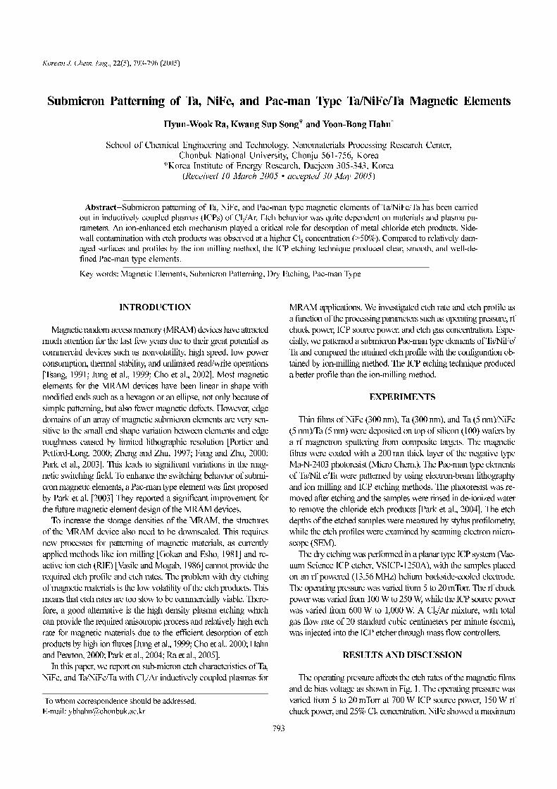
The operating pressure affects the etch rates of the magnetic films
and dc bias voltage as shown in Fig. 1. The operating pressure was
varied from 5 to 20 mTorr at 700 W ICP source power, 150 W rf
chuck power, and 25% Cl2 concentration. NiFe showed a maximum
794 H.-W. Ra et al.
September, 2005
etch rate at 10 mTorr. However, the etch rate of Ta decreased grad-
ually with increasing the operating pressure. In general, the con-
centration of neutrals increases with increasing the pressure, but at
the same time the recombination rate of ions and electrons in the
plasma also increases with pressure [Liberman and Lichtenberg,
1994]. The increase in recombination rate then produces fewer in-
cident ions onto the sample surfaces, resulting in less effect of phys-
ical sputtering on removal of etch products. Hence, the etch rate of
magnetic films decreased at a higher operating pressure mainly due
to the more recombination of ions and shorter mean free path of ions.
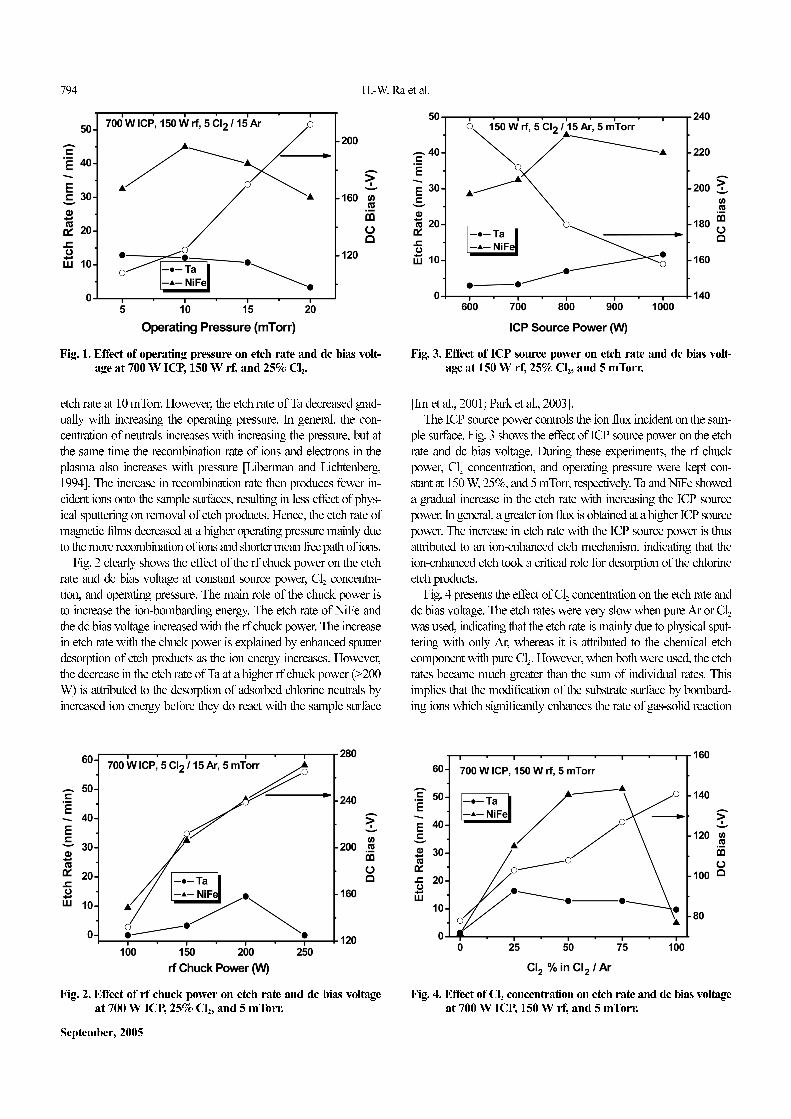
Fig. 2 clearly shows the effect of the rf chuck power on the etch
rate and dc bias voltage at constant source power, Cl2 concentra-
tion, and operating pressure. The main role of the chuck power is
to increase the ion-bombarding energy. The etch rate of NiFe and
the dc bias voltage increased with the rf chuck power. The increase
in etch rate with the chuck power is explained by enhanced sputter
desorption of etch products as the ion energy increases. However,
the decrease in the etch rate of Ta at a higher rf chuck power (>200
W) is attributed to the desorption of adsorbed chlorine neutrals by
increased ion energy before they do react with the sample surface
[Im et al., 2001; Park et al., 2003].
The ICP source power controls the ion flux incident on the sam-
ple surface. Fig. 3 shows the effect of ICP source power on the etch
rate and dc bias voltage. During these experiments, the rf chuck
power, Cl2 concentration, and operating pressure were kept con-
stant at 150 W, 25%, and 5 mTorr, respectively. Ta and NiFe showed
a gradual increase in the etch rate with increasing the ICP source
power. In general, a greater ion flux is obtained at a higher ICP source
power. The increase in etch rate with the ICP source power is thus
attributed to an ion-enhanced etch mechanism, indicating that the
ion-enhanced etch took a critical role for desorption of the chlorine
etch products.
Fig. 4 presents the effect of Cl2 concentration on the etch rate and
dc bias voltage. The etch rates were very slow when pure Ar or Cl2
was used, indicating that the etch rate is mainly due to physical sput-
tering with only Ar, whereas it is attributed to the chemical etch
component with pure Cl2. However, when both were used, the etch
rates became much greater than the sum of individual rates. This
implies that the modification of the substrate surface by bombard-
ing ions which significantly enhances the rate of gas-solid reaction
Fig. 1. Effect of operating pressure on etch rate and dc bias volt-age at 700 W ICP, 150 W rf, and 25% Cl2.
Fig. 2. Effect of rf chuck power on etch rate and dc bias voltageat 700 W ICP, 25% Cl2, and 5 mTorr.
Fig. 3. Effect of ICP source power on etch rate and dc bias volt-age at 150 W rf, 25% Cl2, and 5 mTorr.
Fig. 4. Effect of Cl2 concentration on etch rate and dc bias voltageat 700 W ICP, 150 W rf, and 5 mTorr.

Submicron Patterning of Pac-man Type Ta/NiFe/Ta Magnetic Elements 795
Korean J. Chem. Eng.(Vol. 22, No. 5)
is more important than the nature of the reactive species generated
in plasma. The etch rate of NiFe achieved a maximum value at 75%
Cl2 concentration, but that of Ta decreased with the Cl2 concentra-
tion, which is a behavior observed frequently for the materials pro-
ducing relatively low-volatility etch products. The dc bias voltage
increased with increasing the Cl2 concentration. This may be ex-
plained by the fact that compared to pure Ar discharges, additional
collisional energy losses are present with increasing the Cl2 concen-
tration, resulting in less production of ions [Ra et al., 2004]. The
lower ion flux at a higher Cl2 percentage (>75%) thus explains in
part the lower etch rates with high chlorine content.
The etched features of magnetic films were examined by using
SEM. Fig. 5 shows the SEM micrographs of the Pac-man type ele-
ments of Ta/NiFe/Ta obtained by ion milling (a) and Cl2/Ar ICP
etching (b), respectively. Compared to the clear, smooth and well-
defined pattern by the ICP etching technique, the ion milling method
produced relatively damaged surfaces and profiles mainly due to
the higher ion energy. In this work, it was found that the etch pro-
Fig. 5. SEM images of Pac-man type elements of Ta/NiFe/Ta patterned by ion milling (a) and Cl2/Ar ICP etching (b).
Fig. 6. Low (top) and high (bottom) magnification SEM images of Pac-man type elements of Ta/NiFe/Ta etched with (a) 10% and (b) 50%Cl2 at 700 W ICP, 150 W rf, and 5 mTorr.
796 H.-W. Ra et al.
September, 2005
file of Ta/NiFe/Ta multilayer is quite dependent on the concentra-
tion of Cl2. Fig. 6 shows the low and high magnification SEM images
of the Pac-man type permalloy element etched with two different
Cl2 concentrations of 10% (a) and 50% (b), respectively, at 700 W
ICP source power, 150 W rf chuck power, and 5 mTorr pressure.
The micrographs show quite smooth surface, clean sidewall, con-
tamination free, and anisotropic profile with 10% Cl2, while the side-
wall is contaminated with deposition of etch products with 50%
Cl2. In conclusion, the results obtained from this work indicate that
the ICP etching with Cl2/Ar discharges can be utilized for submi-
cron pattern transfer of the magnetic elements for MRAM devices.
CONCLUSIONS
High density plasma etching of NiFe, Ta, and Pac-man type ele-
ments of Ta/NiFe/Ta was carried out with Cl2/Ar discharges. NiFe
showed a maximum etch rate at an operating pressure of 10 mTorr
while the etch rate of Ta decreased with increasing the pressure.
The etch rate of NiFe and the dc bias voltage increased with the rf
chuck power. Ta showed a gradual increase in the etch rate with
increasing the ICP source power, while the NiFe showed a maxi-
mum etch rate (45 nm/min) at 800 W ICP source power. The etch
rate of NiFe achieved a maximum value at 75% Cl2 concentration,
but that of Ta decreased with Cl2 concentration. Compared to rela-
tively damaged surfaces and profiles by the ion milling method,
the ICP etching technique produced clear, smooth, contamination
free, and well-defined Pac-man type elements.
ACKNOWLEDGMENTS
This paper was supported in part by research funds of Chonbuk
National University and by the NRL program through Korea Insti-
tute of Energy Research.
REREFENCES
Cho, H. G., Kim, Y. K. and Lee, S. R., “Magnetic and Magnetoresis-
tance Properties of Synthetic Spin Valves with Different Pinning Lay-
er Thicknesses,” J. Korean Phys. Soc., 41, 753 (2002).
Cho, H., Lee, K.-P., Jung, K. B., Pearton, S. J., Marburger, J., Sharifi, F.,
Hahn, Y. B. and Childress, J. R., “Corrosion-free Dry Etch Pattern-
ing of Magnetic Random Access Memory Stacks: Effects of Ultra-
violet Illumination,” J. Appl. Phys., 87, 6397 (2000).
Fang, T. N. and Zhu, J. G., “Switching Fluctuations and Density Limita-
tions of Pseudospin Valve Memory,” J. Appl. Phys., 87, 7061 (2000).
Gokan, H. and Esho, S., “Pattern Fabrication by Oblique Incidence Ion-
beam Etching,” J. Vac. Sci. Technol., 18, 23 (1981).
Hahn, Y. B., Hays, D. C., Cho, H., Jung, K. B., Abernathy, C. R., Dono-
van, S. M., Pearton, S. J., Han, J. and Shul, R. J., “Comparison of
ICl- and IBr-based Plasma Chemistries for Inductively Coupled Plas-
ma Etching of GaN, InN and AlN,” Mater. Sci. Eng., B60, 95 (1999).
Hahn, Y. B., Hays, D. C., Cho, H., Jung, K. B., Abernathy, C. R. and
Pearton, S. J., “Effect of Inert Gas Additive Species on Cl2 High Den-
sity Plasma Etching of Compound Semiconductors: Part I. GaAs and
GaSb,” Appl. Surf. Sci., 147, 207 (1999).
Hahn, Y. B. and Pearton, S. J., “A Unified Global Self-Consistent Model
of a Capacitively and Inductively Coupled Plasma Etching System,”
Korean J. Chem. Eng., 17, 304 (2000).
Im, Y. H., Choi, C. S. and Hahn, Y. B., “High Density Plasma Etching
of GaN Films in Cl2/Ar Discharges with a Low-Frequency-Excited
DC Bias,” J. Korean Phys. Soc., 39, 617 (2001).
Jung, K. B., Cho, H., Hahn, Y. B., Hays, D. C., Lambers, E. S., Park,
Y. D., Feng, T., Childress, J. R. and Pearton, S. J., “Effect of Inert
Gas Additive on Cl2-based Inductively Coupled Plasma Etching of
NiFe and NiFeCo,” J. Vac. Sci. Technol. A, 17, 2223 (1999).
Jung, K. B., Cho, H., Hahn, Y. B., Hays, D. C., Lambers, E. S., Park,
Y. D., Feng, T., Childress, J. R. and Pearton, S. J., “Effect of Inert
Gas Additive on Cl2-based Inductively Coupled Plasma Etching of
NiFe and NiFeCo,” J. Vac. Sci. Technol. A, 17, 2223 (1999).
Jung, K. B., Cho, H., Hahn, Y. B., Hays, D. C., Lambers, E. S., Park,
Y. D., Feng, T., Childress, J. R. and Pearton, S. J., “Relative Merits
of Cl2 and CO/NH3 Plasma Chemistries for Dry Etching of Magnetic
Random Access Memory Device Elements,” J. Appl. Phys., 85, 4788
(1999).
Jung, K. B., Cho, H., Hahn, Y. B., Hays, D. C., Lambers, E. S., Park,
Y. D., Feng, T., Childress, J. R. and Pearton, S. J., “Interhalogen Plas-
ma Chemistries for Dry Etch Patterning of Ni, Fe, NiFe and NiFeCo
Thin Films,” Appl. Surf. Sci., 140, 215 (1999).
Liberman, M. A. and Lichtenberg, A. J., Principles of Plasma Discharges
and Materials Processing, John-Wiley and Sons, N. Y. (1994).
Park, H. J., Ra, H.-W., Song, K. S. and Hahn, Y. B., “ Inductively Cou-
pled Plasma Etching of Ta, Co, Fe, NiFe, NiFeCo, and MnNi with
Cl2/Ar Discharges,” Korean J. Chem. Eng., 21, 1235 (2004).
Park, J. S., Park, H. J., Hahn, Y. B., Yi, G.-C. and Yoshikawa, A., “Dry
Etching of ZnO Films and Plasma-induced Damage to Optical Prop-
erties,” J. Vac. Sci. Technol. B, 21, 800 (2003).
Park, M. H., Hong, Y. K., Gee, S. H. and Erickson, D. W., “Magnetiza-
tion Configuration and Switching Behavior of Submicron NiFe Ele-
ments: Pac-man Shape,” Appl. Phys. Lett., 83, 329 (2003).
Portier, X. and Petford-Long, A. K., “The Formation of 360o Domain
Walls in Magnetic Tunnel Junction Elements,” Appl. Phys. Lett., 76,
754 (2000).
Ra, H.-W., Park, H. J., Kim, K. J., Kim, W.-Y. and Hahn, Y.-B., “Dry
Etching of NiFe, NiFeCo, and Ta in Cl2/Ar Inductively Coupled Plas-
ma,” Korean Chem. Eng. Res., 43, 76 (2005).
Ra, H.-W., Hahn, Y. B., Song, K. S., Park, M. H. and Hong, Y. K., “Dry
Etching of NiFe/Co and NiFe/Al-O/Co Multilayers in an Inductively
Coupled Plasma of Cl2/Ar Mixture,” J. Vac. Sci. Technol. A, 22, 2388
(2004).
Tsang, C. H., “Design and Performance Considerations in High Areal
Density Longitudinal Recording (Invited),” J. Appl. Phys., 69, 5393
(1991).
Vartuli, C. B., Pearton, S. J., Lee, J. W., Mackenzie, J. D., Abernathy,
C. R., Shul, R. J., Constantine, C. and Barratt, C., “Inductively Cou-
pled Plasma Etching of III-V Nitrides in CH4/H2/Ar and CH4/H2/N2
Chemistries,” J. Electrochem. Soc., 144, 2844 (1997).
Vasile, M. J. and Mogab, C. J., “Chemically Assisted Sputter Etching
of Permalloy using CO or Cl2,” J. Vac. Sci. Technol. A, 4, 1841
(1986).
Zheng, Y. and Zhu, J. G., “Switching Field Variation in Patterned Sub-
micron Magnetic Film Elements,” J. Appl. Phys., 81, 5471 (1997).