STEEPER D3 4 29June2012 - CORDIS · STEEPER:’’Grant’Agreement’n.’257267’ ’...
15
STEEPER Steep Subthreshold Slope Switches for Energy Efficient Electronics Grant Agreement Number: 257267 Project Acronym: STEEPER Project Title: Steep Subthreshold Slope Switches for Energy Efficient Electronics Funding Scheme: Collaborative project Thematic Area: Information and Communication Technologies Project start date: 01/06/2010 Deliverable D3.4: Power-performance trade-off of simple circuits incorporating Tunnel-FETs Nature 1 : R Dissemination level 2 : PU Due date: Month: M24 Date of delivery: M25 Partners involved: IUNET, EPFL Authors: D. Esseni, M.Gobbesso, B.Kapidani, P.Palestri, T.Rollo, L.Selmi, N. Dagtekin, L. De Michielis, C. Alper, L. Lattanzio, W. Grabinski and A. M. Ionescu Document version:V2 1 R = Report, P = Prototype, D = Demonstrator, O = Other 2 PU = Public, PP = Restricted to other programme participants (including the Commission Services, RE = Restricted to a group specified by the consortium (including the Commission Services), CO = Confidential, only for the members of the consortium (including the Commission Services)
Transcript of STEEPER D3 4 29June2012 - CORDIS · STEEPER:’’Grant’Agreement’n.’257267’ ’...

STEEPER
Steep Subthreshold Slope Switches
for Energy Efficient Electronics
Grant Agreement Number: 257267 Project Acronym: STEEPER Project Title: Steep Subthreshold Slope Switches for Energy Efficient
Electronics Funding Scheme: Collaborative project Thematic Area: Information and Communication Technologies Project start date: 01/06/2010
Deliverable D3.4: Power-performance trade-off of simple circuits incorporating Tunnel-FETs Nature1: R
Dissemination level2: PU Due date: Month: M24 Date of delivery: M25 Partners involved: IUNET, EPFL Authors: D. Esseni, M.Gobbesso, B.Kapidani, P.Palestri, T.Rollo, L.Selmi, N. Dagtekin,
L. De Michielis, C. Alper, L. Lattanzio, W. Grabinski and A. M. Ionescu Document version:V2
1 R = Report, P = Prototype, D = Demonstrator, O = Other 2 PU = Public, PP = Restricted to other programme participants (including the Commission Services, RE = Restricted to a group specified by the consortium (including the Commission Services), CO = Confidential, only for the members of the consortium (including the Commission Services)

STEEPER: Grant Agreement n. 257267 Deliverable D3.4 – Version V2
2
Revision history
Version Date Author Comment
0.1 June 2012 IUNET First issue
1 25 June 2012 Adrian Ionescu Approved without changes
2 29 June 2012 IUNET, KL Diss level back to PU, minor changes to text
Table of Contents 1. Energy efficiency in digital circuits ............................................................................................. 3
2. Device structures and simulation approach..................................................................................... 4
3. Simulation of FO4 inverter chains ................................................................................................. 7
4. Power-speed trade off: technology boosters ................................................................................. 10
4.1 Power - Delay Trade-off.......................................................................................................... 10
4.2. Device Parameters and Simulation Methodology .................................................................. 11
4.3. Results .................................................................................................................................... 12
References: ........................................................................................................................................ 15

STEEPER: Grant Agreement n. 257267 Deliverable D3.4 – Version V2
3
1. Energy efficiency in digital circuits
The average energy dissipated by a digital gate per clock cycle time can be roughly partitioned in a dynamic and a standby or leakage contribution. The dynamic component EDIN can be written as:
EDIN =α QSWVDD (1)
Where α is the activity factor, QSW is the effective charge switched at the output node and VDDis the supply voltage. The energy ELEAK dissipated in a clock cycle time TCLK can be written as:
ELEAK=Ntp tp ILEAK VDD (2)
Where ILEAK is the leakage current of the gate in the standby condition. The cycle time TCLK has been here written as (Ntp tp), where tp is the delay of the gate and Ntpis the ratio (TCLK/tp). In a typical digital system the clock time can be, for instance, from some tens up to more than a hundred times the tp of the inverters in a ring-oscillator.
The scaling of the supply voltage, VDD, is the most powerful measure to scale energy, and it has been used extensively in the last 20 years. In particular, for ambient intelligent applications the design of microprocessors and DSPs has focused on the minimum possible energy per operation, which lead to the demonstration of fast-Fourier transform DSPs with only 155nJ per operation [Wan05] and of processors achieving 1pJ per instruction [Han08,Han082]. The existence of a minimum energy condition can be explained as follows [Wan05]: for an assigned CMOS technology with a given transistor threshold voltage VT, when the VDD is reduced the switching energy decreases but the clock frequency also decreases, which enlarges the clock cycle. Since the leakage energy is proportional to the cycle time, below a given VDD the leakage energy becomes dominant, so that a further VDD reduction increases the overall energy per operation. It has been repeatedly reported that the VDD for minimum energy is smaller than VT, that results in sub-threshold digital circuits working at clock frequencies as low as hundreds of kHz [Wan05,Han08,Han082]. The minimum energy condition is illustrated in Fig.1.
Figure 1: Illustration of the minimum energy operation point and implicit definition of EOPT, VOPT and VMIN.

STEEPER: Grant Agreement n. 257267 Deliverable D3.4 – Version V2
4
In our contribution to Deliverable 3.4 we have studied the tradeoff between delay and energy consumption for three transistor technologies, namely bulk MOSFETs, ultra-thin body SOI (UTB-SOI) MOSFETs and Tunnel FETs realized in an SOI device structure. The delay, leakage energy and dynamic energy is studied as a function of VDD
2. Device structures and simulation approach All the transistors considered in our study have a gate length of 30nm. Fig.2(left)reports a sketch of the double-gate SOI structure used both for UTB-SOI MOSFETs and for Tunnel FETs. The device structure can be considered a scaled version of the single-gate UTB Tunnel FETs defined in the Milestone 3.2.The semiconductor thickness is 10nm and the equivalent oxide thickness is 1.1nm.The doping in the semiconductor film is NSOI=1017cm-3.
In order to improve the on current with respect to unstrained silicon transistors, for the n-type Tunnel FETs we employed aSi0.6Ge0.4 source, and, furthermore, an n+ halo at source-channel junction with Nhalo= 1x1019 cm-3. The Si0.6Ge0.4 source mainly raises the valence band with respect to a silicon source, whereas the shift of the conduction band is negligible, consequently it is not a viable technology booster for the improvement of the on current of p-type Tunnel FETs. Thus, in order to improve the on-current of p-type Tunnel FET we resorted to a large tensile uniaxial strain (+3GPa) throughout the device channel. The corresponding shift of the conduction band was calculated according to [Ung07], while for the valence band we used a six band k·p model [DeM07]; more details about these calculations can be found in [Ess11]. The resulting bandgap for the strained silicon is about 1.004eV. The effect of the strain is accounted for in the SENTAURUS simulations by simply reducing the silicon bandgap to 1.004eV, which remarkably increases the on-current of the p-type Tunnel FETs.
To compare the performance of Tunnel FETs with conventional MOS transistor, we also designed bulk MOSFETs representative of a 32nm bulk CMOS technology. Fig.2(right) shows a sketch of the device structure for the bulk MOSFETs. The equivalent oxide thickness for these transistors is 1.16nm. The channel doping concentration is 1.2x1018cm-3 and, in order to improve the electrostatic integrity, we also used source-drain pockets featuring a peak doping concentration Nhalo= 1.3x1019cm-3.
Figure 2: Sketch of the double-gate SOI structure used both for SOI MOSFETs and for Tunnel FETs (left) and of the device structure used for the bulk MOSFETs.

STEEPER: Grant Agreement n. 257267 Deliverable D3.4 – Version V2
5
All the simulations were performed by using the DESSIS SENTAURUS TCAD tool. The non-local band-to-band-tunneling (BTBT) model was used for the Tunnel FETs. As discussed in Deliverable 3.2, the BTBT parameters for silicon were calibrated against some of the experimental data for tunneling diodes reported in [Sol07].
Fig.3 reports a comparison of the IDS versus VGS characteristics for the n-type and p-type transistors used in our study and for VDS=0.5V. The work-function of the devices was adjusted in order to have an off-current, IOFF, of approximately 10pA/µm for all the transistors; such IOFF
corresponds to the ITRS specification for low standby power (LSTB) applications. The work-functions stemming from this design of the transistors are reported in Tab.1.
As it can be seen the average inverse sub-threshold slope (SS) of Tunnel FETs is significantly smaller than 60mV/decfor IDS ranging in the three decades from IOFF=10pA/µm to roughly 10nA/mm. The SOI MOSFETs have an essentially ideal SS value of 60mV/dec, whereas the SS of bulk MOSFETs is about 82mV/dec. The threshold voltage VT of bulk MOSFETs is quite large in magnitude to allow for IOFF=10pA/mm, which enforced the use of a relatively high work-function for n-type and a relatively low work-function for p-type transistors. The different SS of the devices result in Tunnel FETs that have larger on currents ION than bulk MOSFETs essentially in the entire VDD range below 0.6V explored below for the digital circuits. The crossover between the on-currents of Tunnel FETs and SOI MOSFETs, instead, occurs for VDD around 0.35V.
Figure 3: Simulated IDS versus VGS characteristics of the n-type (left) and p-type (right) transistors and for VDS=0.5V. The UTB-SOI MOSFETs and the Tunnel FETs have the device structure in Fig.2, while bulk MOSFETs are depicted in Fig.3. The x-axis reports the absolute value of the gate to source voltage for both n-type and p-type transistors.
n-type bulk MOSFET
p-type bulk MOSFET
n-type SOI MOSFET
p-type SOI MOSFET
n-type Tunnel FET
p-type Tunnel FET
Workfunction [V]
4.55 4.72 4.61 4.69 4.04 5.11
Table1: Gate work-function for the simulated transistors
Fig.4 reports the simulated gate capacitance CG versus VGS characteristics for the n-type transistors and for VDS=0V or 0.5V, where some interesting trends can be identified. The capacitance of the bulk-MOSFET essentially coincides with the parasitic component, in fact for VGS

STEEPER: Grant Agreement n. 257267 Deliverable D3.4 – Version V2
6
up to 0.5V the transistor is still off and the intrinsic, channel capacitance is negligible. The SOI MOSFETs, instead, because of the smaller VT show a start of the onset of strong inversion in the channel, which results in a CG increase at the largest VGS illustrated in Fig.4. The CG characteristics of Tunnel-FETs are markedly different with respect to MOSFETs and, in particular, the CG is larger especially for VDS=0V. Fig.5 illustrates the gate-drain capacitance CG versus VGS characteristics for the n-type transistors and reveals that, as expected, the large CGof Tunnel FETs is essentially due to the gate-drain capacitance CGD. This can be understood considering the low work-function 4.04V used for n-type Tunnel FETs (see Tab.1), that results in a negative threshold voltage for the MOS capacitor formed by the gate and the n+ drain region. The overall larger gate capacitance of Tunnel FETs has significant implications for the delays of the digital circuits, as illustrated below.
Figure 4: Simulated gate capacitance CG versus VGS characteristics for the n-type transistors.
Figure 5: Simulated gate-drain capacitance CGD versus VGS characteristics for the n-type transistors.
STEEPER: Grant Agreement n. 257267 Deliverable D3.4 – Version V2
7
3. Simulation of FO4 inverter chains
The current and capacitance characteristics illustrated in the previous section clearly show that the MOS transistors work in the sub-threshold regime for digital circuits operating at VDD below approximately 0.5V. We have studied the delay, dynamic and leakage energy in series of fan-out-four (FO4) inverters, whose sizing is increased by four at each stage in order to have approximately the same delay per stage. The circuit is sketched in Fig.6 for a four stage circuit, where the sizing of the first stage is Sn=1. The analysis of the circuits was carried out by using the mixed device-circuit simulation mode of the SENTAURUS TCAD environment.
Figure 6: Sketch of four stages, FO4 inverter chain studied in the circuit simulations.
Fig.7illustrates the static characteristic at VDD=0.6V for the three different transistor types. The logic threshold VLT is close to 0.5VDD for the devices and the static characteristic is well behaved. Thanks to a very large ratio between transconductance and output conductance the SOI MOSFETs are the devices yielding the largest voltage gain at the logic threshold. Fig.8 reports a sample of transient wave-forms at the output of the four inverters for either bulk MOSFETs or Tunnel FETs and for VDD=0.4V. The propagation delay of an inverter in the FO4 circuit has been determined as the propagation delay of the third inverter in the chain, defined as the delay from the time when the input is at half the transition to the time when the output is at half the corresponding transition.
Figure 7: Simulated static characteristics of an inverter obtained by using bulk MOSFETs, SOI MOSFETs or Tunnel FETs. Both n-type and p-type transistors have a unitary sizing for all the technologies.

STEEPER: Grant Agreement n. 257267 Deliverable D3.4 – Version V2
8
Figure 8: Dynamic waveforms for an FO4 series and VDD=0.4V. Left: bulk MOSFETs; right: Tunnel FETs.
Figure 9: Propagation delay of the third inverter in the FO4 inverter chain versus the supply voltage VDD and for the three different transistor types.
Fig.9 reports the propagation delay versus the supply voltage VDDfor bulk MOSFETs, SOI MOSFETs and Tunnel FETs. As VDD decreases from 0.5V to 0.25V the degradation of the delay is larger for MOSFETs than for Tunnel FETs, because these latter do not work in the steep subthreshold region, as it can be seen in Fig.3. As a result the Tunnel FETs inverters become faster than the bulk MOSFETs circuits for VDD below 0.45V and the delay of Tunnel FETs and SOI MOSFETs is comparable for VDD below approximately 0.3V.
Besides the delay, we also analyzed the leakage and dynamic energy of the FO4 inverter chains by using Eqs.1 and 2. To this purpose the leakage current was determined from the simulation of the static characteristics of the inverter, whereas the charge QSW switched during the transients was obtained by using a direct integration of the current absorbed from the supply voltage during the circuit operation. As it can be seen in Eqs.1 and 2, the average EDIN and the ELEAK in a clock cycle depends on the activity factor α and on Ntp=(TCLK/tp), where Ntp is the ratio between the clock time and the VDD dependent delay tp of the inverters.

STEEPER: Grant Agreement n. 257267 Deliverable D3.4 – Version V2
9
Fig.10 illustrates the total average energy per cycle for the three transistors and versus VDD. In these calculations for the energy we used a low activity factor α=0.01 and Ntp=(TCLK/tp)=200. With these parameters we can observe a minimum energy operation for VDD between 0.3V and 0.2V. As it can be seen the minimum energy for Tunnel FETs is observed at VDD =0.25V and it is roughly 0.5fJ, however the minimum energy for the MOSFETs is smaller than for Tunnel FETs. This is mainly ascribed to the larger capacitance of the Tunnel FETs illustrated in Figs.4 and 5 and it is a difference between MOSFETs and Tunnel FETs that deserves further investigation.
Figure 10: Average energy dissipated by an inverter in the FO4 circuit versus VDD calculated by using Eqs.1 and 2 and using ILEAK and QSW values obtained from SENTAURUS simulations.

STEEPER: Grant Agreement n. 257267 Deliverable D3.4 – Version V2
10
4. Power-speed trade off: technology boosters In this chapter of the deliverable, we examine the power-speed trade-off in digital circuitries built with tunnel-FETs and the impact of the device capacitances on the dynamic performance. To this purpose a complementary modling approach will be used with respect to that considered by the IUNET partner. In particular we will use TCAD to compute the IV and CV curves of the devices and circuit simulations based on look-up table models for the circuit level analysis.
4.1 Power - Delay Trade-off
The circuit power dissipation can be expressed as
P=KCVDD2f+ IOFFVDD
where K is the switching activity, C is the total equivalent capacitance being charged and discharged in a clock cycle, and f is the clock frequency. The first term gives the switching or active power, and the second term is leakage or standby power.
One of the simplest means to calculate the intrinsic delay of a device which is adopted by ITRS as well is CGGVDD/ION; ION being the drain current when VGS=VDS=VDD and CGG is the total gate capacitance including fringing capacitance at VGS=VDS [Taur98]. More recently, some effort have been devoted to redefine the capacitance and current such that the same metric can be used to predict the inverter delay by examining dynamic switching events and trajectories of capacitance and current and by approximation of equivalent values for the nonlinear changes [Na02]. For TFETs no such study has been done yet. Therefore only simulation results are presented for the inverter characteristics.
Among the device delay and power, one of the most common circuit design trade-off manifests itself. The higher the supply voltage, the smaller the delay gets since as compared to CGG, the increase in Ion is markedly larger and follows a super-linear (exponential in the sub-threshold region) trend. That is the reason why the highest frequency that the circuit can be clocked increases with VDD. This performance boost comes at an expense of elevation both in the total power consumption and switching energy as explained in the previous chapter. In this three dimensional power-delay-VDD design problem, the choice of threshold voltage gives the solution space resulting in different standby power consumption. The application requirements identify where the optimization should be performed. Therefore it is fairly common to have transistors with various threshold voltages in the design kits aiming to address wide range of applications (high performance: high VDD& low VTH, low power: low VDD& low VTH, and low standby power: low VDD& high VTH).
In this section of the deliverable we do not consider the choice of the threshold voltage but focus on the device level optimization, targeting an absolute improvement in the delay without perturbing the leakage power and somewhat break the power delay trade-off for tunnel-FETs. In this context, the device capacitance plays a key role. If it were possible to reduce the capacitance without degrading the control of the gate and thus the drain current, it would create more room for voltage scaling maintaining certain speed and therefore reduce the active power by twofold impact (C, VDD). From an alternative perspective; higher speed can be achieved for the similar power consumption values.

STEEPER: Grant Agreement n. 257267 Deliverable D3.4 – Version V2
11
4.2. Device Parameters and Simulation Methodology
Circuit design considerations given in 4.1, encourages working on the device capacitance optimization.
Therefore we compare in this section the two TFET structures given in Fig. 11, namely a conventional double gate p-i-n/n-i-p hetero-junction TFET with high-k gate oxide (HeTFET, Fig. 11-top), and an optimized TFET design (HKLKTFET, Fig. 11-bottom) that features a tandem of high-k/ low-k oxides. The source materials for n- and p-type TFETs are Germanium (ND=1e19cm-3) and IndiumArsenide (NA=2e18cm-3) respectively. The intrinsic Silicon region is p-doped (NA=5e15cm-3) and abrupt junctions have been assumed.
The main idea of the optimized structure is that a large gate coupling between the gate terminal and the underlying channel is only needed in the restricted region where the carrier injection mechanism (that is the BTBT) takes place. The remaining part of the channel, where the carrier transport is mainly dictated by the diffusion mechanism, does not need extremely large coupling, thus a gate oxide with a lower dielectric constant can be used without any loose of device performance.
To this purpose, HfO2 has been used as high-k material (ɛr=22), while common SiO2 (ɛr=3.9) has been used as low-k oxide.
Also in this case, the device-level simulations were performed using Synopsys Sentaurus Device2010.12 with a non-local band-to-band tunneling model that dynamically determines the tunneling path direction based on the valence band gradient. The Shockley-Read-Hall recombination model has been activated to account for the trap-assisted tunneling under the high electric field, present in the tunnel junction during device operation.
Figure 11: Top: the conventional heterojunction TFET (HeTFET) and the optimized high-k/low-k architecture (HKLKTFET), bottom, compared in this section. Both devices feature a gate oxide thickness tox=2.5nm, a Silicon thickness tSi=20nm, and a gate length LG=50nm. The metal gate workfunctions are 4.04eV and 5.07eV for n- and p-type respectively.

STEEPER: Grant Agreement n. 257267 Deliverable D3.4 – Version V2
12
Transient simulations are conducted by MMSIM 7.2 with the look-up table based models implemented in VerilogA. The look-up table solution is a two steps approach; the first being quasi-stationary simulations with TCAD (or device measurements) to build the multi-dimensional tables of current and charge with respect to bias voltages and the second step being utilization of these tables by a SPICE-like simulator. The first step must be repeated for any modification in the technology parameter set which makes this approach inflexible. However, once the device parameters are set, table-based models allow simulating complex circuits with a reasonable accuracy and speed. For transient simulations it is possible to replace the charge tables with the capacitance tables which can be extracted by TCAD AC-simulations. This improves the convergence properties which are likely to be poorer with charge tables unless their differentiability and continuous derivatives are guaranteed.
The dynamic current is expressed as
Ixt=IDC,xVGS,VDS+∂Qx∂Vd∂Vd∂t+∂Qx∂Vg∂Vg∂t+∂Qx∂Vs∂Vs∂t
=IDC,x(VGS,VDS)+Cxd∂Vd∂t+Cxg∂Vg∂t+Cxs∂Vs∂t
where x refers to one of the device terminals.
4.3. Results
The major advantages of the HKLKTFET are shown in Fig. 12. In particular, Fig. 12-top shows the progressive reduction of the small signal total gate (Cgg) and gate-to-drain (Cgd) capacitances obtained by reducing the high-k oxide length LHK.
While in MOSFET operating in the linear region, the total gate capacitance is known to be equally distributed between the source and drain terminals, the reverse biased junction at the source channel interface of TFET devices makes the entire gate capacitance to fall upon the drain terminal, causing much higher Cgd (≈Cgg) components [Mookerjea09].
Figure 13 shows the improvements in terms of the subthreshold slope resulting from a more favorable electrostatic configuration, as explained in [Alper12]. It should be observed that the restriction of the high-k oxide to the sole narrow region where the BTBT generation takes place does not degrade the on-current level of the device.
Figure12: total gate capacitance (left) and gate-to-drain capacitance (right) for the HKLKTFET as a function of the gate voltage, for different high-k lengths.

STEEPER: Grant Agreement n. 257267 Deliverable D3.4 – Version V2
13
Figure13: transfer characteristics for different higk-k length. It can be observed that the restriction of the high-k oxide to the BTBT region does not degrade the on current level and it offers at the
same time an improved subthreshold slope.
The intrinsic delay versus supply voltage curve is given in Figure 14. As expected from the device characteristics, intrinsic delay has been reduced by factor of ~2 for the entire Vdd range of interest by optimization of the gate oxide.
Figure14: Intrinsic Delay of the InAs tunnel-FET with and without Low-K region
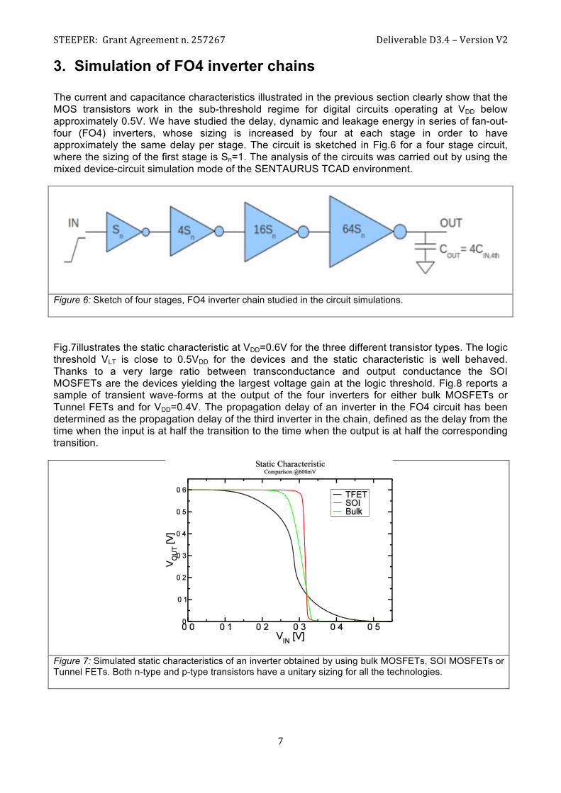
To predict the circuit level benefits of the technology booster presented here,an inverter chain composed of 3 identical inverter stages is simulated at frequency of 1MHz. The variation of the F01 delay which corresponds to the delay of the middle stage is given in Figure 15. With the non-uniform gate oxide, the improvement on circuit delay is around factor ~2.5 inside the entire range of supply voltages simulated.
STEEPER: Grant Agreement n. 257267 Deliverable D3.4 – Version V2
14
Figure 15: Fan-out 1 delay of the inverters based on tunnel-FETs with and without Low-K region
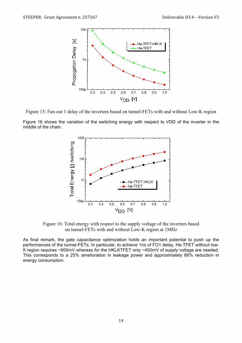
Figure 16 shows the variation of the switching energy with respect to VDD of the inverter in the middle of the chain.
Figure 16: Total energy with respect to the supply voltage of the inverters based on tunnel-FETs with and without Low-K region at 1MHz
As final remark, the gate capacitance optimization holds an important potential to push up the performances of the tunnel-FETs. In particular, to achieve 1ns of FO1 delay, He-TFET without low-К region requires ~600mV whereas for the HKLKTFET only ~450mV of supply voltage are needed. This corresponds to a 25% amelioration in leakage power and approximately 66% reduction in energy consumption.

STEEPER: Grant Agreement n. 257267 Deliverable D3.4 – Version V2
15
References:
[DeM07] M. De Michieliset al. IEEE Trans. onElectr. Devices, vol. 54, no. 9, pp. 2164–2173, Sep. 2007. [Ess11] D.Esseniet al. “Nanoscale MOS Transistors – Semi-classical Transport and Applications”, Cambridge UniversityPress 2011. [Han08] S. Hanson et al.,IEEE J. Solid-State Circuits, vol. 43, no. 4, pp. 881–891, 2008. [Han082] S. Hanson et al.,IEEE Trans. onElectr. Devices, vol. 55, no. 1, pp. 175-184, 2008. [Sol04] P.M.Solomonet al., Journal of Applied Physics, vol. 95, no. 10, pp. 5800-5812. [Ung07] E. Ungersboecket al., IEEE Trans. on Electr. Devices, Vol.54, no.9, pp.2183–2190, 2007. [Wan05] A. Wanget al., IEEE J. Solid-State Circuits, vol. 40, no. 1, 2005. [Taur98] Y. Taur, Tak H. Ning, “Fundamentals of Modern VLSI Devices”, Cambiridge University Press 1998. [Na02] M. H. Na et al. Electron Devices Meeting, 2002.pg: 121 - 124 [Alper12] C. Alper et al, submitted to ESSDERC2012 [Sentaurus11] Synopsys Sentaurus Device Used Maual [Mookerjea09] S. Mookerjea et al. IEEE TED ,vol 56, 2092-2098, Sept 2009.