
SPICE { A Spatial Parallel Architecture for Accelerating...
192
SPICE 2 – A Spatial Parallel Architecture for Accelerating the SPICE Circuit Simulator Thesis by Nachiket Kapre In Partial Fulfillment of the Requirements for the Degree of Doctor of Philosophy California Institute of Technology Pasadena, California 2010 (Submitted October 26, 2010)
Transcript of SPICE { A Spatial Parallel Architecture for Accelerating...

SPICE2 – A Spatial ParallelArchitecture for Accelerating the
SPICE Circuit Simulator
Thesis by
Nachiket Kapre
In Partial Fulfillment of the Requirements
for the Degree of
Doctor of Philosophy
California Institute of Technology
Pasadena, California
2010
(Submitted October 26, 2010)

c© 2010
Nachiket Kapre
All Rights Reserved
ii

Abstract
Spatial processing of sparse, irregular floating-point computation using a single FPGA
enables up to an order of magnitude speedup (mean 2.8× speedup) over a conven-
tional microprocessor for the SPICE circuit simulator. We deliver this speedup us-
ing a hybrid parallel architecture that spatially implements the heterogeneous forms
of parallelism available in SPICE. We decompose SPICE into its three constituent
phases: Model-Evaluation, Sparse Matrix-Solve, and Iteration Control and parallelize
each phase independently. We exploit data-parallel device evaluations in the Model-
Evaluation phase, sparse dataflow parallelism in the Sparse Matrix-Solve phase and
compose the complete design in streaming fashion. We name our parallel architec-
ture SPICE2: Spatial Processors Interconnected for Concurrent Execution for ac-
celerating the SPICE circuit simulator. We program the parallel architecture with a
high-level, domain-specific framework that identifies, exposes and exploits parallelism
available in the SPICE circuit simulator. This design is optimized with an auto-tuner
that can scale the design to use larger FPGA capacities without expert intervention
and can even target other parallel architectures with the assistance of automated
code-generation. This FPGA architecture is able to outperform conventional proces-
sors due to a combination of factors including high utilization of statically-scheduled
resources, low-overhead dataflow scheduling of fine-grained tasks, and overlapped
processing of the control algorithms.
We demonstrate that we can independently accelerate Model-Evaluation by a
mean factor of 6.5×(1.4–23×) across a range of non-linear device models and Matrix-
Solve by 2.4×(0.6–13×) across various benchmark matrices while delivering a mean
combined speedup of 2.8×(0.2–11×) for the two together when comparing a Xilinx
iii

Virtex-6 LX760 (40nm) with an Intel Core i7 965 (45nm). With our high-level frame-
work, we can also accelerate Single-Precision Model-Evaluation on NVIDIA GPUs,
ATI GPUs, IBM Cell, and Sun Niagara 2 architectures.
We expect approaches based on exploiting spatial parallelism to become impor-
tant as frequency scaling slows down and modern processing architectures turn to
parallelism (e.g. multi-core, GPUs) due to constraints of power consumption. This
thesis shows how to express, exploit and optimize spatial parallelism for an important
class of problems that are challenging to parallelize.
iv

Contents
Abstract iii
1 Introduction 1
1.1 Contributions . . . . . . . . . . . . . . . . . . . . . . . . . . . . . . . 2
1.2 SPICE . . . . . . . . . . . . . . . . . . . . . . . . . . . . . . . . . . . 7
1.3 FPGAs . . . . . . . . . . . . . . . . . . . . . . . . . . . . . . . . . . . 9
1.4 Implementing SPICE on an FPGA . . . . . . . . . . . . . . . . . . . 11
2 Background 15
2.1 The SPICE Simulator . . . . . . . . . . . . . . . . . . . . . . . . . . 15
2.1.1 Model-Evaluation . . . . . . . . . . . . . . . . . . . . . . . . . 17
2.1.2 Matrix Solve . . . . . . . . . . . . . . . . . . . . . . . . . . . . 19
2.1.3 Iteration Control . . . . . . . . . . . . . . . . . . . . . . . . . 20
2.2 SPICE Performance Analysis . . . . . . . . . . . . . . . . . . . . . . 22
2.2.1 Total Runtime . . . . . . . . . . . . . . . . . . . . . . . . . . . 22
2.2.2 Runtime Scaling Trends . . . . . . . . . . . . . . . . . . . . . 23
2.2.3 CMOS Scaling Trends . . . . . . . . . . . . . . . . . . . . . . 25
2.2.4 Parallel Potential . . . . . . . . . . . . . . . . . . . . . . . . . 26
2.3 Historical Review . . . . . . . . . . . . . . . . . . . . . . . . . . . . . 31
2.3.1 FPGA-based SPICE solvers . . . . . . . . . . . . . . . . . . . 35
2.3.2 Our FPGA Architecture . . . . . . . . . . . . . . . . . . . . . 36
3 Model-Evaluation 38
3.1 Structure of Model-Evaluation . . . . . . . . . . . . . . . . . . . . . . 39
v

3.1.1 Parallelism Potential . . . . . . . . . . . . . . . . . . . . . . . 41
3.1.2 Specialization Potential . . . . . . . . . . . . . . . . . . . . . . 42
3.2 Related Work . . . . . . . . . . . . . . . . . . . . . . . . . . . . . . . 43
3.3 Verilog-AMS Compiler . . . . . . . . . . . . . . . . . . . . . . . . . . 46
3.4 Fully-Spatial Implementation . . . . . . . . . . . . . . . . . . . . . . 47
3.5 VLIW FPGA Architecture . . . . . . . . . . . . . . . . . . . . . . . . 51
3.5.1 Operator Provisioning . . . . . . . . . . . . . . . . . . . . . . 53
3.5.2 Static Scheduling . . . . . . . . . . . . . . . . . . . . . . . . . 55
3.5.3 Scheduling Techniques . . . . . . . . . . . . . . . . . . . . . . 56
3.5.3.1 Conventional Loop Unrolling . . . . . . . . . . . . . 57
3.5.3.2 Software Pipelining with GraphStep Scheduling . . . 58
3.6 Methodology and Performance Analysis . . . . . . . . . . . . . . . . . 62
3.6.1 Toolflow . . . . . . . . . . . . . . . . . . . . . . . . . . . . . . 62
3.6.2 FPGA Hardware . . . . . . . . . . . . . . . . . . . . . . . . . 63
3.6.3 Optimized Processor Baseline . . . . . . . . . . . . . . . . . . 64
3.6.4 Overall Speedups . . . . . . . . . . . . . . . . . . . . . . . . . 65
3.6.5 Speedups for Different Verilog-AMS Device Models . . . . . . 66
3.6.6 Effect of Device Complexity on Speedup . . . . . . . . . . . . 68
3.6.7 Understanding the Effect of Scheduling Strategies . . . . . . . 71
3.6.8 Effect of PE Architecture on Performance . . . . . . . . . . . 72
3.6.9 Auto-Tuning System Parameters . . . . . . . . . . . . . . . . 74
3.7 Parallel Architecture Backends . . . . . . . . . . . . . . . . . . . . . . 76
3.7.1 Parallel Architecture Potential . . . . . . . . . . . . . . . . . . 77
3.7.2 Code Generation . . . . . . . . . . . . . . . . . . . . . . . . . 80
3.7.3 Optimizations . . . . . . . . . . . . . . . . . . . . . . . . . . . 82
3.7.4 Auto Tuning . . . . . . . . . . . . . . . . . . . . . . . . . . . . 82
3.8 Results: Single-Precision Parallel Architectures . . . . . . . . . . . . 84
3.8.1 Performance Analysis . . . . . . . . . . . . . . . . . . . . . . . 85
3.8.2 Explaining Performance . . . . . . . . . . . . . . . . . . . . . 89
3.9 Conclusions . . . . . . . . . . . . . . . . . . . . . . . . . . . . . . . . 90
vi

4 Sparse Matrix Solve 92
4.1 Structure of Sparse Matrix Solve . . . . . . . . . . . . . . . . . . . . 92
4.1.1 Structure of the KLU Algorithm . . . . . . . . . . . . . . . . . 94
4.1.2 Parallelism Potential . . . . . . . . . . . . . . . . . . . . . . . 99
4.2 Dataflow FPGA Architecture . . . . . . . . . . . . . . . . . . . . . . 103
4.3 Related Work . . . . . . . . . . . . . . . . . . . . . . . . . . . . . . . 108
4.3.1 Parallel Sparse Matrix Solve for SPICE . . . . . . . . . . . . . 108
4.3.2 Parallel FPGA-based Sparse Matrix Solvers . . . . . . . . . . 109
4.3.3 General-Purpose Parallel Sparse Matrix Solvers . . . . . . . . 110
4.4 Experimental Methodology . . . . . . . . . . . . . . . . . . . . . . . . 111
4.4.1 FPGA Implementation . . . . . . . . . . . . . . . . . . . . . . 114
4.5 Results . . . . . . . . . . . . . . . . . . . . . . . . . . . . . . . . . . . 115
4.5.1 Exploring Opportunity for Iterative Solvers . . . . . . . . . . 115
4.5.2 Sequential Baseline: KLU with spice3f5 . . . . . . . . . . . . 116
4.5.3 Parallel FPGA Speedups . . . . . . . . . . . . . . . . . . . . . 118
4.5.4 Limits to Parallel Performance . . . . . . . . . . . . . . . . . . 121
4.5.5 Impact of Scaling . . . . . . . . . . . . . . . . . . . . . . . . . 124
4.6 Conclusions . . . . . . . . . . . . . . . . . . . . . . . . . . . . . . . . 126
5 Iteration Control 127
5.1 Structure in Iteration Control Phase . . . . . . . . . . . . . . . . . . 127
5.2 Performance Analysis . . . . . . . . . . . . . . . . . . . . . . . . . . . 129
5.3 Components of Iteration Control Phase . . . . . . . . . . . . . . . . . 132
5.4 Iteration Control Implementation Framework . . . . . . . . . . . . . . 136
5.5 Hybrid FPGA Architecture . . . . . . . . . . . . . . . . . . . . . . . 138
5.6 Methodology and Results . . . . . . . . . . . . . . . . . . . . . . . . . 140
5.6.1 Integration with spice3f5 . . . . . . . . . . . . . . . . . . . . 140
5.6.2 Mapping Flow . . . . . . . . . . . . . . . . . . . . . . . . . . . 141
5.6.3 Hybrid VLIW FPGA Implementation . . . . . . . . . . . . . . 142
5.6.4 Microblaze Implementation . . . . . . . . . . . . . . . . . . . 144
vii

5.6.5 Comparing Application-Level Impact . . . . . . . . . . . . . . 145
5.7 Conclusions . . . . . . . . . . . . . . . . . . . . . . . . . . . . . . . . 147
6 System Organization 148
6.1 Modified SPICE Solver . . . . . . . . . . . . . . . . . . . . . . . . . . 148
6.2 FPGA Mapping Flow . . . . . . . . . . . . . . . . . . . . . . . . . . . 149
6.3 FPGA System Organization and Partitioning . . . . . . . . . . . . . 152
6.4 Complete Speedups . . . . . . . . . . . . . . . . . . . . . . . . . . . . 153
6.5 Comparing different Figures of Merit . . . . . . . . . . . . . . . . . . 154
6.6 FPGA Capacity Scaling Analysis . . . . . . . . . . . . . . . . . . . . 158
7 Conclusions 159
7.1 Contributions . . . . . . . . . . . . . . . . . . . . . . . . . . . . . . . 162
7.2 Lessons . . . . . . . . . . . . . . . . . . . . . . . . . . . . . . . . . . 163
8 Future Work 165
8.1 Parallel SPICE Roadmap . . . . . . . . . . . . . . . . . . . . . . . . . 165
8.1.1 Precision of Model-Evaluation Phase . . . . . . . . . . . . . . 165
8.1.2 Scalable Dataflow Scheduling for Matrix-Solve Phase . . . . . 166
8.1.3 Domain Decomposition for Matrix-Solve Phase . . . . . . . . 166
8.1.4 Composition Languages for Integration . . . . . . . . . . . . . 166
8.1.5 Additional Parallelization Opportunities in SPICE . . . . . . . 167
8.2 Broad Goals . . . . . . . . . . . . . . . . . . . . . . . . . . . . . . . . 168
8.2.1 System Partitioning . . . . . . . . . . . . . . . . . . . . . . . . 168
8.2.2 Smart Auto-Tuners . . . . . . . . . . . . . . . . . . . . . . . . 168
8.2.3 Fast Online Placement and Routing . . . . . . . . . . . . . . . 168
8.2.4 Fast Simulation . . . . . . . . . . . . . . . . . . . . . . . . . . 170
8.2.5 Fast Design-Space Exploration . . . . . . . . . . . . . . . . . . 170
8.2.6 Dynamic Reconfiguration and Adaptation . . . . . . . . . . . 171
Bibliography 172
viii

Chapter 1
Introduction
This thesis shows how to expose, exploit and implement the parallelism available in
the SPICE simulator [1] to deliver up to an order of magnitude speedup (mean 2.8×
speedup) on a single FPGA chip. SPICE (Simulation Program with Integrated Cir-
cuit Emphasis) is an analog circuit simulator that can take days or weeks of runtime
on real-world problems. It models the analog behavior of semiconductor circuits us-
ing a compute-intensive non-linear differential equation solver. SPICE is notoriously
difficult to parallelize due to its irregular, unpredictable compute structure, and a
sloppy sequential description. It has been observed that less than 7% of the floating-
point operations in SPICE are automatically vectorizable [2]. SPICE is part of the
SPEC92 [3] benchmark collection which is a set of challenge problems for micropro-
cessors. Over the past couple of decades, we have relied on innovations in computer
architecture (clock frequency scaling, out-of-order execution, complex branch predic-
tors) to speedup applications like SPICE. It was possible to improve performance of
existing application binaries by retaining the exact same ISA (Instruction Set Archi-
tecture) abstraction at the expense of area and power consumption. However, these
traditional computer organizations have now run up against a power wall [4] that
prevents further improvements using this approach. More recently, we have migrated
microprocessor designs towards “multi-core” organizations [5, 6] which are an ad-
mission that further improvements in performance must come from parallelism that
will be explicitly exposed to the hardware. Reconfigurable, spatial architectures like
FPGAs provide an alternate platform for accelerating applications such as SPICE
1

SPICE Phase Description Parallelism Compute Organization
Model Evaluation Verilog-AMS Data Parallel Statically-Scheduled VLIWMatrix Solve Sparse Graph Sparse Dataflow Token Dataflow
Iteration Control SCORE Streaming Sequential Controller
Table 1.1: Thesis Research Matrix
at lower clock frequencies and lower power. Unlike multi-core organizations which
can exploit a fixed amount of instruction-level parallelism, thread-level parallelism
and data-level parallelism, FPGAs can be configured and customized to exploit par-
allelism at multiple granularities as required by the application. FPGAs offer higher
compute density [7] by implementing computation using spatial parallelism which
distributes processing in space rather than time. In this thesis, we show how to trans-
late the high compute density available on a single-FPGA to accelerate SPICE by
2.8× (11× max.) using a high-level, domain-specific programming framework. The
key questions addressed in this thesis as follows:
1. Can SPICE be parallelized? What is the potential for accelerating SPICE?
2. How do we express the irregular parallel structure of SPICE?
3. How do we use FPGAs to exploit the parallelism available in SPICE?
4. Will FPGAs outperform conventional multi-core architectures for parallel SPICE?
We intend to use SPICE as a design-driver to address broader questions. How
do we capture, exploit and manage heterogeneous forms of parallelism in a single
application? How do we compose the parallelism in SPICE to build the integrated
solution? Is it sufficient to constrain this parallelism to a general-purpose architecture
(e.g. Intel multi-core)? Will the performance of this application scale easily with
larger processing capacities?
1.1 Contributions
We develop a novel framework to capture and reason about complex applications
like SPICE with heterogeneous forms of parallelism. We use parallel patterns for
2

expressing and unifying this parallelism effectively. We organize our parallelism on
reconfigurable architecture to spatially implement and customize the compute orga-
nization to each style of parallelism. We configure this hardware with a compilation
flow supported by auto-tuning to implement the parallelism in a scalable manner
on available resources. We use SPICE as a design driver to experiment with these
ideas and quantitatively demonstrate the benefits of this design philosophy.
As shown in the matrix in Table 1.1, we first decompose SPICE into its three
constituent phases: (1) Model Evaluation, (2) Sparse Matrix-Solve and (3) Iteration
Control. We describe these phases in Chapter 2.
We identify opportunities for parallel operation in the different phases of SPICE
and provide design strategies for hardware implementation using suitable parallel
patterns. Parallel patterns are a paradigm of structured concurrent program-
ming that help us express, capture and organize parallelism. Paradigms and patterns
were identified in the classic paper by Floyd [8]. They are invaluable tools and tech-
niques for describing computer programs in a methodical “top-down” manner. When
describing parallel computation, we need similar patterns for organizing our parallel
program. We can always expose available parallelism in the most general Communi-
cating Sequential Processes (CSP [9]) model of computation. However, this provides
no guidance for managing communication and synchronization between the parallel
processes. It also does not necessarily provide any insight into choosing the right
hardware implementation for the parallelism. In contrast, parallel patterns are
reusable strategies for describing and composing parallelism that serve two key pur-
poses. First, these patterns let the programmer construct the parallel program from
well-known, primitive, building blocks that can compose with each other. Second,
the patterns also provide structure for constructing parallel hardware that best im-
plements the computation. This is more restricted than the general CSP model but
simplifies the task of writing the parallel program and developing parallel hardware
using well-developed solutions to avoid common pitfalls.
We analyze the structure of SPICE in the form of patterns and illustrate how
they guide the selection of parallel FPGA organization. The Model-Evaluation phase
3

of SPICE can be effectively parallelized using the data-parallel pattern. We imple-
ment this data-parallelism in a software-pipelined fashion on the FPGA hardware.
We further exploit the static nature of this data-parallel computation to schedule the
computation on a custom, time-multiplexed, VLIW architecture. We extract the ir-
regular, sparse dataflow parallelism available in the Matrix-Solve phase of SPICE that
is different from the regular, data-parallel pattern that characterizes Model-Evaluation
phase. We use the KLU matrix-solver package to expose the static dataflow paral-
lelism available in this phase and develop a distributed, token-dataflow architecture
for exploiting that parallelism. This static dataflow capture allows us to distribute the
graph spatially across parallel compute units and process the graph in a fine-grained
fashion. Finally, we express the Iteration-Control phase of SPICE using a stream-
ing pattern in the high-level SCORE framework to enable overlapped evaluation and
efficiently implement the SPICE analysis state machines.
We now describe some key ideas that help us develop our parallel FPGA imple-
mentation:
• Domain-Specific Framework: The parallelism in SPICE is a heterogeneous
composition of multiple parallel domains. To properly capture and exploit par-
allelism in SPICE, we develop domain-specific flows which include high-level lan-
guages and compilers customized for each domain. We develop a Verilog-AMS
compiler to describe the non-linear differential equations for Model-Evaluation.
We use the SCORE [10] framework (TDF language and associated compiler
and runtime) to express the Iteration-Control phase of SPICE and compose the
complete design. This high-level problem capture makes the spatial, parallel
structure of the SPICE program evident. We can then use the compiler and
develop auto-tuners to exploit this spatial structure on FPGAs.
• Specialization: The SPICE simulator requires three inputs: (1) Circuit (2)
Device type and parameters (3) Convergence/Termination control options. We
exploit the static and early-bound nature of certain inputs to generate optimized
hardware implementation and quantify their benefits. The Model Evaluation
4

computation is dependent on device type and the device parameters. We can
pre-compile, optimize and schedule the static dataflow computation for the few
device types used by SPICE and simply select the appropriate type prior to
execution. We get an additional improvement in performance and reduction
in area by specializing the device evaluation to specific device parameters that
are common to specific semiconductor manufacturing processes. We quantify
the benefits of specialization in Table 3.4 in Chapter 3. The Sparse Matrix
Solve computation operates on a dataflow graph that can be extracted at the
start of the simulation. This early-bound structure of the computation allows
us to distribute and place operations on our parallel architecture once and then
reuse the placement throughout the simulation. We show a 1.35× improvement
in sequential performance of Matrix-Solve phase through specialization in Ta-
ble 4.5 from Chapter 4. Finally, the simulator convergence and terminal control
parameters are loaded into registers at the start of the simulation and are used
by the hardware to manage the SPICE iterations.
• Spatial Architectures: The different parallel patterns in SPICE can be
efficiently implemented on customized spatial architectures on the FPGA. Hence,
we identify and design the spatial FPGA architecture to match the pattern of
parallelism in the SPICE phases. Our statically-scheduled VLIW architecture
delivers high utilization of floating-point resources (40–60%) and is supported
by an efficient time-multiplexed network that balances the compute and com-
municate operations. We use a Token-Dataflow architecture to spatially dis-
tribute processing of the sparse matrix factorization graph across the paral-
lel architecture. The sparse graph representation also eliminates the need for
address-calculation and sequential memory access dependencies that constrain
the sequential implementation. Finally, we develop a streaming controller that
enables overlapped processing of the Iteration Control computation with the
rest of SPICE.
• Scalability: Typical FPGA designs are rigidly tied to a particular FPGA fam-
5

ily and require a complete redesign to scale to larger FPGA sizes. We are inter-
ested in developing scalable FPGA systems that can be automatically adapted
to use extra resources when they become available. For speedup calculations in
this thesis, our parallel design is engineered to fit into the resources available
on a single Virtex-6 LX760 FPGA. We develop an auto-tuner that enables easy
scalability of our design to larger FPGA capacities. Our auto-tuner explores
area-memory-time space to pick the implementation that fits available resources
while delivering the highest performance. The Model-Evaluation and Iteration-
Control phases of SPICE can be accelerated almost linearly with additional
logic and memory resources. With a sufficiently large FPGA we can spatially
implement the complete dataflow graph of the Model-Evaluation and Iteration-
Control computation as a physical circuit without using a time-shared VLIW
architecture. Furthermore, the auto-tuner can automatically choose the proper
configuration for this larger FPGA. This is relevant in light of the recently an-
nounced Xilinx Virtex-7 FPGA family [11] that has 2–3× the capacity of the
FPGA we use in this thesis. However, the Sparse Matrix-Solve phase will only
enjoy limited additional parallelism with extra resources. Additional research
into decomposed matrix solvers is necessary to properly scale performance on a
larger system.
The quantitative contributions of this thesis include:
1. Complete simulator: We accelerate the complete double-precision implemen-
tation of the SPICE simulator by 0.2-11.1× when comparing the Xilinx Virtex-6
LX760 (40nm technology node) with an Intel Core i7 965 processor (45nm tech-
nology node) with no compromise in simulation quality.
2. Model-Evaluation Phase: We implement the Model-Evaluation phase by
compiling a high-level Verilog-AMS description to a statically-scheduled custom
VLIW architecture. We demonstrate a speedup of 1.4–23.1× across a range of
non-linear device models when comparing Double-Precision implementations on
a Virtex-6 LX760 compared to an Intel Core i7 965. We also deliver speedups
6

of 4.5–123.5× for a Virtex-5 LX330, 10.1–63.9× for an NVIDIA 9600GT GPU,
0.4–6× for an ATI FireGL 5700 GPU, 3.8–16.2× for an IBM Cell and 0.4–1.4×
for a Sun Niagara 2 architectures when comparing Single-Precision evaluation
to an Intel Xeon 5160 across these architectures at 55nm–65nm technology. We
also show speedups of 4.5–111.6× for a Virtex-6 LX760, 13.1–133.1× for an
NVIDIA GTX285 GPU and 2.8–1200× for an ATI Firestream 9270 GPU when
comparing Single-Precision evaluation to an Intel Core i7 965 on architectures
at 40–55nm technology.
3. Sparse Matrix-Solve Phase: We implement the sparse dataflow graph rep-
resentation of the Sparse Matrix-Solve computation using a dynamically-routed
Token Dataflow architecture. We show how to improve the performance of irreg-
ular, sparse matrix factorization by 0.6–13.4×when comparing a 25-PE parallel
implementation on a Xilinx Virtex-6 LX760 FPGA with a 1-core implementa-
tion on an Intel Core i7 965 for double-precision floating-point evaluation.
4. Iteration-Control Phase: Finally, we compose the complete simulator along
with the Iteration-Control phase using a hybrid streaming architecture that
combines static scheduling with limited dynamic selection. We deliver 2.6×
(max 8.1×) reduction in runtime for the SPICE Iteration-Control algorithms
when comparing a Xilinx Virtex-6 LX760 with an Intel Core i7 965.
1.2 SPICE
We now present an overview of the SPICE simulator and identify opportunities for
parallel operation. At the heart of the SPICE simulator is a non-linear differential
equation solver. The solver is a compute-intensive iterative algorithm that requires an
evaluation of non-linear physical device equations and sparse matrix factorizations in
each iteration. When the number of devices in the circuit grows, the simulation time
will increase correspondingly. As manufacturing process technologies keep improving
we are able to build smaller semiconductor devices and consequently we can pack
7

larger circuits into a single chip. The ITRS roadmap for semiconductors [12, 13]
suggests that SPICE simulation runtimes for modeling non-digital effects [12] and
large power-ground networks [13] are a challenge. This will increase the size of the
circuits (N) we want to simulate. SPICE simulation time scales as O(N1.2) which
outpaces the increase in computing capacity of conventional architectures O(N0.96) as
shown in Figure 1.1 (additional discussion in Section 2.2). Our parallel, single-FPGA
design scales more favorably with increasing circuit size as O(N0.7). We show the
peak capacities of the processor and FPGA used in the comparison in Table 1.2. A
parallel SPICE solver will decrease verification time and reduce the time-to-market
for integrated circuits. However, as identified in [2] parallelizing SPICE is hard. Over
the past three decades, parallel SPICE efforts have either delivered limited speedups
or sacrificed simulation quality to improve performance. Furthermore, the techniques
and solutions are specific to a particular system and not easily portable to newer,
better architectures. The SPICE simulator is a complex mix of multiple compute
patterns that demands customized treatment for proper parallelization. After a
careful performance analysis, it is clear that the Model Evaluation and Sparse Matrix-
Solve phases of SPICE are the key contributors to total SPICE runtime. We note that
the Model Evaluation phase of SPICE is in fact embarrassingly parallel by itself and
should be relatively easy to parallelize. We describe our parallel solution in Chapter 3.
In contrast, the Sparse Matrix-Solve phase is more challenging. This is one of the
key reasons why earlier studies were unable to parallelize the complete simulator.
The underlying compute structure of Sparse Matrix Solve is irregular, unpredictable
and consequently performs poorly on conventional architectures. Recent advances
in numerical algorithms provide an opportunity to reduce these limitations. We
use the KLU solver [14, 15] to generate an irregular, dataflow factorization graph
that exposes the available parallelism in the computation. We explain our approach
for parallelizing the challenge Sparse Matrix-Solve phase in Chapter 4. Finally, the
Iteration-Control phase of SPICE is responsible for co-ordinating the simulation steps.
While it is a tiny fraction of sequential runtime, it may become a non-trivial fraction
of the accelerated SPICE solver. We show how to efficiently implement the Iteration-
8

101
102
103
104
105
80486
Pentiu
m
Pentiu
m 2
Pentiu
m 3
Pentiu
m 4
Xeon 5
160
Core
i7
106
107
108
109
FLO
PS
Transistors
N0.96
(a) CPU Double-Precision FLOPS
10-4
10-3
10-2
10-1
100
102
103
104
105
Runtim
e/Ite
ration (
s)
Circuit Size
N0.7
N1.2
sequential CPUparallel FPGA
(b) SPICE Runtime
Figure 1.1: Scaling Trends for CPU FLOPS and spice3f5 runtime
Family Chip Tech. Clock Peak GFLOPS Power(nm) (GHz) (Double) (Watts)
Intel Core i7 965 45 3.2 25 130Xilinx Virtex-6 LX760 40 0.2 26 20–30
Table 1.2: Peak Floating-Point Throughputs (Double-Precision)
Control phase of SPICE in Chapter 5. Finally, in Chapter 6 we discuss how to
integrate the complete SPICE solver on a single FPGA.
1.3 FPGAs
We briefly review the FPGA architecture and highlight some key characteristics of an
FPGA that make it well-suited to accelerate SPICE. A Field-Programmable Gate Ar-
ray is a massively-parallel architecture that implements computation using hundreds
of thousands of tiny programmable computing elements called LUTs (lookup tables)
connected to each other using a programmable communication fabric. Typically these
LUTs are clustered into SLICEs (2–4 LUTs per SLICE depending on FPGA archi-
tecture). Moore’s Law delivers progressively larger FPGA capacities with increasing
numbers of SLICEs per chip. Modern FPGAs also include hundreds of embedded
memories and integer multipliers distributed across the fabric for concurrent oper-
ation. We show a small region inside an island-style FPGA in Figure 1.2 (LUTs
9

LUT
LUT LUT
LUT LUT
LUT LUT
LUT
LUT LUT
EmbeddedSRAM
IntegerMultiplier
Switchbox
Connectionbox
Figure 1.2: A Small Region of an FPGA
10

correspond to islands in a sea of interconnect). An FPGA allows us to configure
the computation in space rather than time and evaluate multiple operations concur-
rently in a fine-grained fashion. In Figure 1.3, we show a simple calculation and its
conceptual implementation on a CPU and an FPGA. For a CPU implementation, we
process the instructions stored in an instruction memory temporally on an ALU while
storing the intermediate results (i.e. variables) in a data memory. On an FPGA, we
can implement the operations as spatial circuits while implementing the dependencies
between the operations physically using pipelined wires instead of variables stored in
memory. Additionally a pipelined FPGA circuit implementation of certain operations
in the computation (e.g. divide, sqrt) require multiple cycles on the CPU while we
can configure a custom, pipelined circuit for those operations on the FPGA for higher
throughput.
While FPGAs have been traditionally successful at accelerating highly-parallel,
communication-rich algorithms and application kernels, they are a challenging tar-
get for mapping a complete application with diverse computational patterns such
as the SPICE circuit simulator. Furthermore, programming an FPGA with exist-
ing techniques for high performance requires months of effort and low-level tuning.
Additionally, these designs do not automatically scale for larger, newer FPGA capac-
ities that become available with technology scaling and require re-compilation and
re-optimization by an expert.
1.4 Implementing SPICE on an FPGA
We now briefly describe our hardware architecture and mapping flow for implementing
SPICE on a single FPGA. We use a high-level framework to express, extract and
compose the parallelism in the different phases of SPICE. We develop a hybrid FPGA
architecture that combines custom architectures tailored to the parallelism in each
phase of SPICE. In Figure 1.4 we show a high-level block diagram of the composite
FPGA architecture with the three regions tailored for each phase of SPICE. We show
a simple picture of our mapping flow in Figure 1.5. While the logic configuration
11

adda addb
div
sqrt
addaaddbdiv
sqrt
ALU
a1a2b1b2d1d2s1o1
a1 a2 b1 b2
d1 d2
s1
o1
temporal spatialcomputation
instr. data
LUT
LUT LUT
LUT LUT
LUT LUT
LUT
LUT LUT
EmbeddedSRAM
IntegerMultiplier
LUT
LUT LUT
LUT LUT
LUT LUT
LUT
LUT LUT
EmbeddedSRAM
IntegerMultiplier
LUT
LUT LUT
LUT LUT
LUT LUT
LUT
LUT LUT
EmbeddedSRAM
IntegerMultiplier
LUT
LUT LUT
LUT LUT
LUT LUT
LUT
LUT LUT
EmbeddedSRAM
IntegerMultiplier
addb
div
sqrt
adda
Figure 1.3: Implementing Computation
of the FPGA is the same for all SPICE circuits, we need to program the FPGA
memories in an instance-specific manner for each circuit we simulate. We show how
we assemble the FPGA hardware and provide additional details of our mapping flow
in Chapter 6.
A completely spatial implementation of the SPICE circuit simulator is too large
to fit on a single FPGA at 40nm technology today. On larger FPGAs, in the near
future, it will become possible to fit the fully-spatial Model Evaluation graphs entirely
on a single FPGA. For these graphs, the cost of a fully-spatial implementation gets
amortized across several device evaluations. However, for the Sparse Matrix-Solve
phase, the limited amount of parallelism and low reuse does not motivate a fully-
spatial design even if we have large FPGAs. Furthermore, configuring the FPGA
for every circuit using FPGA CAD tools (synthesize logic, place LUTs, and route
wires) can itself take hours or days of runtime defeating the purpose of a parallel
FPGA implementation for SPICE. We develop the custom FPGA architecture using
virtual organizations capable of accommodating the entire SPICE simulator operation
on a single FPGA. Furthermore, we simplify our circuit-specific compilation step by
requiring only a memory generation step to program the virtual architecture (static
12

ModelEvaluation
Device Parameters and State
SparseMatrixSolve
Dataflow GraphStructure
Iteration Controller
2 3
1SimulationOptions
DRAM
FPGA
Figure 1.4: Block-Diagram of the SPICE FPGA Solver
schedule or graph structure).
13

SPICE Circuit
Prepare FPGAMemories
FPGA LogicConfiguration A
Run SPICE onFPGAs
Custom VLIW
TokenDataflow
StreamArch.
FPGA LogicConfiguration B
FPGA LogicConfiguration C
Tra
nsis
t or
mod
el
bsim3
bsim4
mos3
Figure 1.5: FPGA Mapping Flow for SPICE
14

Chapter 2
Background
In this chapter, we review the SPICE simulation algorithm and discuss the inner-
workings of the three constituent phases of SPICE. We review existing literature and
categorize previous attempts at parallelizing SPICE. We argue that these previous
approaches were unable to fully capitalize on the parallelism available within the
SPICE simulator due to limitations of hardware organizations and inefficiencies in
the software algorithms. In the following chapters, we will describe our FPGA-based
“spatial” approach that provides a communication-centric architecture for exploiting
the parallelism in SPICE.
2.1 The SPICE Simulator
SPICE simulates the dynamic analog behavior of a circuit described by its constituent
non-linear differential equations. It was developed at the EECS Department of the
University of California, Berkeley by Donald Pederson, Larry Nagel [1], Richard New-
ton, and many other contributors to provide a fast and robust circuit simulation
program capable of verifying integrated circuits. It was publicly announced thirty-
seven years ago in 1973 and many versions of the package have since been released.
spice2g6 was part of the SPEC89 and SPEC92 benchmark sets of challenge problems
for microprocessors. Many commercial versions of analog circuit simulators inspired
by SPICE now exist as part of a large IC design and verification industry. For this
study, we use the open-source spice3f5 package released from Berkeley in 1995.
15

Matrix A[i], Vector b [i]
Vector x [i]
Vector x [i-1]
ModelEvaluationStep(per device)
SPICEIteration
Non-Linear Converged?
Increment timestep?
Transient Iterations
Newton-Raphson Iterations
Matrix SolverA[i].x[i]=b[i]
Matrix A[i], Vector b [i]
SPICE Deck:Circuit, Options
Voltage, Current Waveforms
Figure 2.1: Flowchart of a SPICE Simulator
SPICE circuit equations model the linear (e.g. resistors, capacitors, inductors)
and non-linear (e.g. diodes, transistors) behavior of devices and the conservation
constraints (i.e. Kirchoff’s current laws—KCL) at the different nodes and branches
of the circuit. SPICE solves the non-linear circuit equations by alternately computing
small-signal linear operating-point approximations for the non-linear elements and
solving the resulting system of linear equations until it reaches a fixed point. The
linearized system of equations is represented as a solution of A~x = ~b, where A is
the matrix of circuit conductances, ~b is the vector of known currents and voltage
quantities and ~x is the vector of unknown voltages and branch currents.
Spice3f5 uses the Modified Nodal Analysis (MNA) technique [16] to assemble
circuit equations into matrix A. The MNA approach is an improvement over conven-
tional nodal analysis by allowing proper handling of voltage sources and controlled
current sources. It requires the application of Kirchoff’s Current Law at all the nodes
in the circuit with voltage at each node being an unknown. It then introduces un-
16

V1 D1
R1
+
_
GND
C1
1 2
Figure 2.2: SPICE Circuit Example
knowns for currents through branches to allow voltage sources and controlled current
sources to be represented.
The simulator calculates entries in A and ~b from the device model equations that
describe device transconductance (e.g., Ohm’s law for resistors, transistor I-V charac-
teristics) in the Model-Evaluation phase. It then solves for ~x using a sparse-direct
linear matrix solver in the Matrix-Solve phase. We show the steps in the SPICE
algorithm in Figure 2.1. The inner loop iteration supports the operating-point calcu-
lation for the non-linear circuit elements, while the outer loop models the dynamics
of time-varying devices such as capacitors. The simulator loop management controls
are handled by the Iteration Control phase. We illustrate the operation of the
simulator using an example shown in Figure 2.2. We first write down the non-linear
differential equations that capture circuit behavior in Equation 2.1–Equation 2.6.
The non-linear (diode) and time-varying (capacitor) devices are represented using
linearized forms in Equation 2.2 and Equation 2.3 respectively. We then reassemble
these equations into A~x = ~b form shown in Figure 2.4.
2.1.1 Model-Evaluation
In the Model-Evaluation phase, the simulator computes conductances and currents
through different elements of the circuit and updates corresponding entries in the
matrix with those values. We expand the equations for the example circuit in Fig-
17

I(R1) = (V1 − V2) ·1
R1(2.1)
I(D1) = Geq(D1) · V2 + Ieq(D1) (2.2)
I(C1) = Geq(C1) · V2 + Ieq(C1) (2.3)
I(V 1) = I(R1) (2.4)
I(R1) = I(C1) + I(D1) (2.5)
V1 = V 1 (2.6)
Figure 2.3: Circuit Equations from Conservations Laws (KCL)
G1 −G1 1−G1 G1 +Geq(C1) +Geq(D1) 0
1 0 0
× V1
V2I(V 1)
=
0Ieq(C1) + Ieq(D1)
V 1
Figure 2.4: Matrix Representation of Circuit Equations in SPICE
ure 2.5 and fill-in the matrix appropriately in Figure 2.6. For the linear elements (e.g.
resistors) this needs to be done only once at the start of the simulation (shown in
blue in Figures 2.5 and 2.6). For non-linear elements, the simulator must search
for an operating-point using Newton-Raphson iterations which requires repeated
evaluation of the model equations multiple times per timestep (inner loop labeled
Newton-Raphson Iterations in Figure 2.1 and shown in red in Figure 2.5 and 2.6).
For time-varying components, the simulator must recalculate their contributions at
each timestep based on voltages at several previous timesteps. This also requires
repeated re-evaluations of the device-model (outer loop labeled Transient Iterations
in Figure 2.1 and shown in green in Figure 2.5 and 2.6).
I(R1) = (V1 − V2) ·G1 (2.7)
I(C1) = (2 · C1
δt) · V2 − (
2 · C1
δt· V old
2 + Iold(C1)) (2.8)
I(D1) = (Isvj· eV2/vj) · V2 + Is · (eV2/vj − 1) (2.9)
Figure 2.5: Circuit Equations with contributions from devices
18

G1 −G1 1−G1 G1 + (2 · C1/δt) 0
+(Is/vj) · eV2/vj
1 0 0
·
V1V2
I(V 1)
=
0
−((2 · C1/δt)× V old2 + Iold(C1))
+Is · (eV2/vj − 1)V 1
Figure 2.6: Matrix contributions from the different devices
A · ~x = ~b (2.10)
L · U · ~x = ~b (2.11)
L · ~y = ~b (2.12)
U · ~x = ~y (2.13) a11 a12 a13a21 a22 a23a31 a32 a33
· x1x2x3
=
b1b2b3
(2.14)
1 0 0l21 1 0l31 l32 1
· u11 u12 u13
0 u22 u230 0 u33
· x1x2x3
=
b1b2b3
(2.15)
1 0 0l21 1 0l31 l32 1
· y1y2y3
=
b1b2b3
(2.16)
u11 u12 u130 u22 u230 0 u33
· x1x2x3
=
y1y2y3
(2.17)
Figure 2.7: Matrix Solve Stages
2.1.2 Matrix Solve
The simulator spice3f5 uses the Modified Nodal Analysis (MNA) technique [16] to
assemble circuit equations into matrix A. Since circuit elements (N) tend to be con-
nected to only a few other elements, there are a constant number (O(1)) of entries per
row of the matrix. Thus, the MNA circuit matrix with O(N2) entries is highly sparse
with O(N) nonzero entries (≈99% of the matrix entries are 0). The matrix structure
is mostly symmetric with the asymmetry being added by the presence of independent
sources (e.g. input voltage source) and inductors. The underlying non-zero struc-
ture of the matrix is defined by the topology of the circuit shown in Figure 2.2 and
19

consequently remains unchanged throughout the duration of the simulation. In each
iteration of the loop shown in Figure 2.1, only the numerical values of the non-zeroes
are updated in the Model-Evaluation phase of SPICE with contributions from the
non-linear elements. To find the values of unknown node voltages and branch currents
~x, we must solve the system of linear equations A~x = ~b as shown in Equation 2.14.
The sparse, direct matrix solver used in spice3f5 first reorders the matrix A to mini-
mize fill-in using a technique called Markowitz reordering [17]. This tries to reduce the
number of additional non-zeroes (fill-in) generated during LU factorization. It then
factorizes the matrix by dynamically determining pivot positions for numerical sta-
bility (potentially adding new non-zeros) to generate the lower-triangular component
L and upper-triangular component U such that A = LU as shown in Equation 2.15.
Finally, it calculates ~x using Front-Solve L~y = ~b (see Equation 2.16) and Back-Solve
U~x = ~y operations (see Equation 2.17).
2.1.3 Iteration Control
The SPICE iteration controller is responsible for two kinds of iterative loops shown
in Figure 2.1: (1) inner loop: linearization iterations for non-linear devices and (2)
outer loop: adaptive time-stepping for time-varying devices. The Newton-Raphson
algorithm is responsible for computing the linear operating-point for the non-linear
devices like diodes and transistors. Additionally, an adaptive time-stepping algorithm
based on truncation error calculation (Trapezoidal approximation, Gear approxima-
tion) is used for handling the time-varying devices like capacitors and inductors. The
controller also implements the loops in a data-dependent manner using customized
convergence conditions and local truncation error estimations.
Convergence Condition: The simulator declares convergence when two con-
secutive iterations generate solution vectors and non-linear approximations that are
within a prescribed tolerance respectively. We show the condition used by SPICE to
determine if an iteration has converged in Equation 2.18 and Equation 2.19. Here, ~Vi
or ~Ii represent the voltage or current unknowns in the i-th iteration of the Newton-
Raphson loop. The convergence conditions compare the current solution vector in
20

iteration (i) with the previous iteration (i − 1). SPICE also performs a similar con-
vergence check on the non-linear function described in the Model-Evaluation. The
closeness between the values in consecutive iterations is parametrized in terms of
user-specified tolerance values: reltol (relative tolerance), abstol (absolute tolerance),
and vntol (voltage tolerance).
|~Vi − ~Vi−1| ≤ reltol ·max (|~Vi|, |~Vi−1|) + vntol (2.18)
|~Ii − ~Ii−1| ≤ reltol ·max (|~Ii|, |~Ii−1|) + abstol (2.19)
Typical values for these tolerances parameters are: reltol=1e− 3 (accuracy of 1
part in 1000), abstol=1e−12 (accuracy of 1 picoampere) and vntol=1e−6 (accuracy
of 1 µvolt). This means the simulator will declare convergence when the changes in
voltage and current quantities get smaller than the convergence tolerances.
Local Truncation Error (LTE): Local Truncation Error is a local estimate
of accuracy of the Trapezoidal approximation used for integration. The truncation-
error-based time-stepping algorithm in spice3f5 computes the next stepsize δn+1 as
a function of the LTE (ε) of the current iteration and a Trapezoidal divided-difference
approximation (DD3) of the charges (x) at a few previous iterations. The equation
for stepsize is shown in Equation 2.20. For a target LTE, the Iteration Controller
can match the stepsize to the rate of change of circuit quantities. If the circuit
quantities are changing too rapidly, it can slow down the simulation by generating
finer timesteps. This allows the simulator to properly resolve the rapidly changing
circuit quantities. In contrast, if the circuit is quiescent (e.g. digital circuits between
clock edges), the simulator can take larger timesteps for a faster simulation. When
the change in the circuit quantities is small, a detailed simulation at fine timesteps
will be a waste of work. Instead, the simulator can advance the simulation with larger
stepsizes. A tolerance parameter trtol provides the user additional control over tuning
the timestep sizes. This parameter (default trtol=7) can be increased if necessary
to avoid excessively fine timesteps. The stepsize δn+1 is added to the current timestep
to advance the simulation as shown in Equation 2.21.
21

10-4
10-3
10-2
10-1
100
102
103
104
105
106
Runtim
e/Ite
ration (
s)
Circuit Size
N1.2
runtimefit
Figure 2.8: Sequential Runtime of spice3f5 for circuit benchmarks
δn+1 =
√trtol · ε
max ( |DD3(x)|12
, abstol)(2.20)
tn+1 = tn + δn+1 (2.21)
2.2 SPICE Performance Analysis
In this section, we discuss important performance trends and identify performance
bottlenecks and characteristics that motivate our parallel approach. We use spice3f5
running on an Intel Core i7 965 for these experiments.
2.2.1 Total Runtime
We first measure total runtime of spice3f5 across a range of benchmark circuits
on an Intel Core i7 965. We use a lightweight timing measurement scheme using
hardware-performance counters (PAPI [18]) that does not impact the actual runtime
of the program. We tabulate the size of the circuits used for this measurement along
with other circuit parameters in Table 4.2. We graph the runtimes as a function of
circuit size in Figure 2.8. We observe that runtime scales as O(N1.2) as we increase
22

10
20
30
40
50
60
70
80
90
100
102
103
104
105
Perc
ent of T
ota
l R
untim
e
Circuit Size
55%
38%
7%
modelevalmodeleval(mean)
matsolvematsolve(mean)
ctrlctrl(mean)
Figure 2.9: Sequential Runtime Breakdown of spice3f5 across the three phases
circuit size N . What contributes to this runtime? To understand this, we break down
the contribution to total runtime from the different phases of SPICE in Figure 2.9.
We observe that, for most cases, total runtime is dominated by the Model-Evaluation
Phase. This is because the circuit is mostly composed of non-linear transistor ele-
ments. In some cases, the Sparse Matrix Solve phase can be a significant fraction of
total runtime. This is true for circuits with large parasitic components (e.g. capaci-
tors, resistors) where the non-linear devices are a small portion of total circuit size.
Finally, the control algorithm that sequences and manages SPICE iterations ends up
taking a small fraction of total runtime. This suggests that in our parallel solution
we must deliver high speedups for the intensive Model-Evaluation and Sparse Matrix
Solve phases of SPICE while ensuring that we do not ignore the control algorithms. If
we do not parallelize the Iteration Control phase, it may create a sequential bottleneck
due to Amdahl’s Law.
2.2.2 Runtime Scaling Trends
Why does SPICE runtime scale super-linearly when we increase circuit size? The
Model-Evaluation component of total runtime increases linearly with the number of
non-linear devices being simulated (approximately O(N1.1) rather than the expected
23

10-4
10-3
10-2
10-1
100
102
103
104
105M
odelE
val R
untim
e/Ite
ration (
ms)
Non-Linear Devices
N1.1
(a) Model-Evaluation Runtime
10-6
10-5
10-4
10-3
10-2
10-1
102
103
104
105M
atr
ixS
olv
e R
untim
e/Ite
ration (
ms)
Circuit Size
N1.2
(b) Matrix-Solve Runtime
Figure 2.10: Scaling Trends for the key phases of spice3f5
O(N) due to limited cache capacity of the processor; also see Figure 2.13(a)) as
shown in Figure 2.10(a). The Matrix-Solve component of runtime empirically grows
as O(N1.2) as shown in Figure 2.10(b) (also see Figure 2.13(b) for floating-point
operation trends). Overall, we observe from Figure 2.8 that runtime grows as O(N1.2)
where N is the size of the circuit.
What other factors impact overall runtime? In Figure 2.11(a), we observe that
floating-point instructions constitute only≈20%–40% of total instruction count (smaller
fraction for larger circuits). The remaining instructions are integer and memory ac-
cess operations that support the floating-point work. These instructions are purely
overhead and can be implemented far more efficiently using spatial FPGA hard-
ware. They also consume instruction cache capacity and issue bandwidth, limiting
the achievable floating-point peak. Furthermore, we observe that increasing circuit
sizes results in higher L2 cache misses. We see L2 cache miss rates as high as 30%–
70% L2 for our benchmarks in Figure 2.11(b). As we increase circuit size, the sparse
matrix and circuit vectors spill out of the fixed cache capacity leading to a higher
cache miss rate. For the benchmarks we use, the sparse matrix storage exceeds the
256KB per-core L2 cache capacity of an Intel Core i7 965 for all except a few small
benchmarks. We also show the overflow factor (Memory required/Cache size) for our
benchmarks in Figure 2.11(b). A parallel architecture for accelerating SPICE has the
24

10
20
30
40
50
60
70
80
90
100
102
103
104
105
Flo
ating-P
oin
t P
erc
ent
Circuit Size
(a) Floating-Point Instruction Fraction
20
30
40
50
60
70
80
102
103
104
105 0.01
0.1
1
10
100
Cache M
iss P
erc
ent
Cache O
verf
low
Facto
r
Circuit Size
(b) L2 Cache Miss Rate
Figure 2.11: Instruction and Memory Scaling Trends for spice3f5
opportunity to properly distribute data across multiple, onchip, embedded memories
and manage communication operations (i.e. moving data between memories) to de-
liver good performance. Our FPGA architecture exploits spatial parallelism, even
in the non-floating-point portion of the computation, to deliver high speedup.
2.2.3 CMOS Scaling Trends
As we continue to reap the benefits of Moore’s Law [19], we need to simulate increas-
ingly larger circuits using SPICE. As we saw in the previous Section 2.2.2, sequential
SPICE runtimes scales as O(N1.2) where N=size of the circuit. This means sequential
SPICE runtimes will get increasingly slower as we scale to denser circuits. Further-
more, as we shrink device feature sizes to finer geometries, we must model increas-
ingly detailed physical effects in the analog SPICE simulations. This will increase the
amount of time spent performing Model-Evaluation [20] as shown in Figure 2.12(a).
For example, the mos1 MOSFET model implements the Shichman-Hodges equations
which are adequate for discrete transistor designs. The semi-empirical mos3 model
was originally developed for integrated CMOS short-channel transistors at 1–2µm
or larger. The new bsim3v3 and bsim4 models are more accurate and commonly
used for today’s technology. It may become necessary to use different models for RF
simulations (psp model) or bipolar transistors (mextram).
25

10
100
1000
10000
10 100 1000
Sequential C
PU
Tim
e/D
evic
e (
ns)
Device Parameters (Complexity)
jfet bjt
bsim3
bsim4
pspmextram
mos1
mos3vbic
hbt
(a) Impact of Non-Linear Device Complexity
101
102
103
104
105
106
ram2k ram8k ram64k
SP
ICE
Runtim
e/Ite
ration (
ns)
Circuits
without parasiticswith parasitics
(b) Impact of Parasitics
Figure 2.12: Impact of CMOS Scaling on SPICE
At smaller device sizes, our circuits will suffer the impact of tighter coupling
and interference between the circuit elements. This will add additional modeling
requirement of parasitic elements (e.g. capacitors, resistors) which increase the size
of the matrix. This will, in turn, increase the time spent in the Sparse Matrix-Solve
phase. The increase in SPICE runtime per iteration due to inclusion of parasitic
effects is shown in Figure 2.12(b).
2.2.4 Parallel Potential
We now try to identify the extent of parallelism available in the two computationally-
intensive phases of SPICE. In Figure 2.13(a), we plot the total number of floating-
point operations as well as the latency of the Model-Evaluation computation assuming
ideal parallel hardware as a function of the number of non-linear elements in the
circuit. The amount of work grows linearly (O(N)) with the number of non-linear
devices. However, the latency of the evaluation remains unchanged at the latency
of a single device evaluation. Each non-linear device can be independently evaluated
with local terminal voltages as inputs and local currents and conductances as outputs.
Thus, the amount of parallelism is proportional to the number of non-linear devices
in the circuit. This phase is embarrassingly parallel, and we show how to exploit this
parallelism in Chapter 3.
26

104
105
106
107
108
101
102
103
104
10510
1
102
103
104
105
Opera
tions
Late
ncy
Non-Linear Circuit Elements
N1
N0
workfit(work)latency
fit(latency)
(a) Total Work and Critical Latency Trends for the Model-Evaluation Phase
103
104
105
106
107
101
102
103
104
10510
2
103
104
105
106
Opera
tions
Late
ncy
Circuit Size
N1.4
N0.7
workfit(work)latency
fit(latency)
(b) Total Work and Critical Latency Trends for the Matrix-Solve Phase
Figure 2.13: Identifying Parallel Potential: Work vs. Latency
27

In Figure 2.13(b), we plot the total number of floating-point operations in the
Sparse Matrix-Solve phase of SPICE as well as the critical path latency as a function
of circuit size. Here, we observe that the amount of work in the sparse factorization
increases as O(N1.4) (compared to O(N3) for dense factorization). This growth rate
is an empirical observation that is valid for circuit matrices in our benchmark set
(see [21]). This explains the O(N1.2) growth in total runtime we previously observed
in Figure 2.8. The critical path latency of the factorization only grows as O(N0.7).
This suggests that a well-designed parallel architecture can extract parallelism from
this phase since the critical path is not growing as fast as N . An architecture with low-
latency communication and lightweight fine-grained spatial processing of operations
should allow us to achieve faster operation.
28

Year
Ref.
Nam
eK
ey
Idea
Para
llel
Hard
ware
Sequenti
al
Base
line
PE
sSp
eedup
SP
ICE
ph
ase
Exp
ress
ion
Acc
ura
cyT
rad
eoff
1979
[22]
-Sta
tic
Dat
aflow
--
100
72.8
Mat
rix
Sol
veD
atafl
owgr
aph
Non
e
1985
[23]
-V
ecto
rta
skgr
aph
S81
0ve
ctor
S81
0sc
alar
48.
9M
atri
xSol
veV
ecto
rize
dgr
aph
Non
e
1986
[24]
Cay
enne
Runti
me
Sch
eduling
VA
X88
00sc
alar
(spice2)
21.
7A
llM
aste
r-Sla
veF
ortr
andec
omp.
Non
e
1987
[25]
SA
PC
ust
omiz
edD
atap
ath
Cust
omSIM
DV
AX
8650
(spice2)
22
All
Com
piled
-Code
Non
e
1988
[26]
-V
ecto
rta
skgr
aph
Allia
nt
FX
/81
PE
(ADVICE)
67.
3A
llShar
ed-M
emor
yN
one
1990
[27]
Par
aspic
eV
ecto
rta
skgr
aph
Allia
nt
FX
/80
1P
E(spice2)
84.
5A
llShar
ed-M
emor
y,P
aral
lel
task
sN
one
1992
[28]
AW
SIM
-3C
ompiled
-C
ode
VL
IWC
ust
ompro
-to
typ
eSun-3
/60
-56
0A
llC
ompiled
-Code
Tab
le-
look
up
1992
[29]
PSP
LA
XW
avef
orm
re-
laxat
ion
Allia
nt
FX
/80
1P
E8
6.1
Rel
ax-
Not
spice3
1993
[30]
Con
cise
Wav
efor
mre
-la
xat
ion
sym
ult
s201
0SP
AR
Cst
a-ti
on19
287
Rel
ax-
Not
spice3
1993
[31]
PA
CE
Dat
aflow
sched
uling
4-ch
ipi8
60SP
AR
C2
43.
7A
llO
fflin
esc
hed
ul-
ing
Non
e
1995
[32]
Spar
taD
atafl
owsc
hed
uling
Fuji
tsu
AP
-10
001
PE
6416
.5A
llM
essa
ge-P
assi
ng
Non
e
1995
[33]
OSC
AR
Tas
ksc
hed
ul-
ing
Cust
om1
PE
84.
3A
llC
ode-
gener
atio
nSin
gle-
Pre
cisi
on19
99[3
4]T
ransp
ute
r-SP
ICE
Blo
ckD
ecom
-p
osit
ion
Ult
raX
LT
ransp
ute
r-
7-
Mat
rix
Sol
ve“P
aral
lel
C”
Non
e
Tab
le2.
1:T
axon
omy
ofP
aral
lel
SP
ICE
App
roac
hes
inth
ep
ast
29

Year
Ref.
Nam
eK
ey
Idea
Para
llel
Hard
ware
Sequenti
al
Base
line
PE
sSp
eedup
SP
ICE
ph
ase
Exp
ress
ion
Acc
ura
cyT
rad
eoff
Rec
ent
Appro
aches
2000
[35]
Xyce
Iter
ativ
eM
a-tr
ixSol
veSG
IO
rigi
n20
001
PE
4024
All
Mes
sage
-Pas
sing
(MP
I)N
one
2002
[36]
SM
P-
SP
ICE
Mult
i-th
read
ing
Hit
achi
9000
N40
001
thre
ad8
4.6
All
Cw
ith
PT
hre
ads
Non
e
2006
[37]
SIL
CA
Appro
x.
-1
thre
adspice3
17.
4A
llSeq
uen
tial
code
PW
L,
etc
2007
[38]
Op
enM
P-
SP
ICE
Dat
a-P
aral
lel
Ult
raSP
AR
C3
1th
read
spice3
41.
3M
odel
Eva
l.spice3f5
wit
hO
pen
MP
Non
e
2008
[39]
Wav
epip
eSp
ecula
tive
Par
alle
lism
4dual
-cor
eSM
P1
thre
ad8
2.4
Iter
.C
trl
Explici
tP
Thre
ads
Non
e
2009
[40]
AC
CIT
-N
SR
Dat
a-par
alle
lA
TI
Fir
e-Str
eam
9170
4-co
reA
MD
Phen
om32
050
Model
Eva
l.D
ata-
par
alle
lB
rook
[41]
Non
e
2009
[42]
Nas
centr
icD
ata-
par
alle
lN
VID
IA88
00G
TS
1-co
reIn
tel
Cor
e212
83
Model
Eva
l.D
ata-
Par
alle
lC
UD
A[4
3,44
]Sin
gle-
Pre
cisi
on20
09[4
5]D
DD
omai
n-
Dec
omp
osit
ion
FW
Gri
d[4
6]1
thre
adspice3f5
3211
9M
atri
xSol
veC
wit
hP
ET
Sc
[47]
pac
kage
Non
e
FP
GA
-bas
edA
ppro
aches
1995
[48]
TIN
Abas
edon
AW
SIM
-323
Xilin
xX
C40
05ch
ips
--
-A
llM
icro
asm
As-
sem
bly
Tab
le-
look
up
1997
[49]
-par
tial
-eva
lA
lter
aF
lex10
KSP
AR
Cst
a-ti
on3
27.7
Model
Eva
l.P
EC
ompiler
Csu
bse
tF
ixed
-p
oint
2003
[50]
SP
Oan
alyti
cal
tran
sfor
mX
ilin
xSpar
-ta
n3
--
-A
llSim
ulink
grap
hs
fixed
-p
oint
Tab
le2.
2:T
axon
omy
ofR
ecen
tP
aral
lel
SP
ICE
Ap
pro
ach
esan
dF
PG
A-b
ased
Syst
ems
30

2.3 Historical Review
We now review the various studies and research projects that have attempted to par-
allelize SPICE in the past three decades or so. These studies attempt to accelerate the
computation using a combination of parallel hardware architectures and/or numerical
software algorithms that are more amenable to parallel evaluation. We tabulate and
classify these approaches in Table 2.1 and Table 2.2. We can refine the classification
of parallel SPICE approaches by considering underlying trends and characteristics of
the different systems as follows:
1. Compute Organization: We see parallel SPICE solvers using a range of
different compute organizations including conventional multi-processing, multi-
core, VLIW, SIMD and Vector.
2. Precision: Under certain conditions, SPICE simulations can efficiently model
circuits at lower precisions.
3. Compiled Code: In many cases, it is possible to generate efficient instance-
specific simulations by specializing the simulator for a particular circuit.
4. Scheduling: Parallel computation exposed in SPICE must be distributed
across parallel hardware elements for faster operation. Many designs develop
novel, custom scheduling solutions that are applicable under certain structural
considerations of the circuit or matrix.
5. Numerical Algorithms: Different classes of circuits perform better with a
suitable choice of a matrix factorization algorithm. Our FPGA design may
benefit from new ideas for factoring the circuit matrix.
6. SPICE Algorithms: Conventional SPICE simulations often perform needless
computation across multiple iterations that is not strictly necessary for an ac-
ceptable result. In many cases, it is possible to rapidly advance simulation time
by exploiting parallelism (e.g. speculation, concurrent alternatives). Our paral-
31

lel FPGA system can enjoy the benefits of exposing parallelism in the iteration
management algorithms.
We now roughly organize the evolution of parallel SPICE systems into five ages
and identify the appropriate category for the systems considered:
Age of Starvation (1980-1990): In the early days of VLSI scaling, the amount
of computing resources available was limited. This motivated designs of custom ac-
celerator systems for SPICE that were assembled from discrete components (e.g. [25,
51, 26]). Numerical algorithms for SPICE were still being developed and not directly
suitable for parallel evaluation. The systems scavenged parallelism in SPICE using
compiled-code approaches and customized hardware. In a compiled-code approach,
the framework produces code for an instance of the circuit and compiles this gen-
erated code for the target architecture. This exposes instance-specific parallelism in
SPICE to the compiler in two primary ways: (1) it enables static optimization of
recurring, redundant work in the Model Evaluation phase and (2) it disambiguates
memory references for the sparse matrix access. The resulting compiled-code pro-
gram is capable of only simulating the particular circuit instance. One of the earliest
papers [22] on parallel SPICE sketches a design for the sparse matrix-solve phase by
extracting the static triangulation graph for the matrix factorization but ignores com-
munication costs. Other studies have also considered extracting the static dataflow
graph for matrix factorization using the MVA (Maximal Vectorization Algorithm)
approach [23] (Compiled Code). The resulting graph is vectorized onto a Hitachi
S810 supercomputer to get a 8.9× speedup with 4 vector units and a modest increase
in storage of intermediate results. Vectorization and simpler address calculation are
key reasons for this high speedup. Cayenne [24] maps the SPICE computation to
a 2-processor VAX system (Compute Organization) running a multiprocessing
operating-system VMS but achieves a limited speedup of 1.7×. A custom design for
a SPICE accelerator with 2 PEs [25] running a Compiled Code SPICE simulation
shows a speedup of 2× over a VAX 8650 operating at ≈2× the frequency. It empha-
sizes parallelizing addressing and memory lookup operations within the Processing
Element (PE) in a manner similar to our customized FPGA designs. Another Com-
32

piled Code simulator outlined in [26] delivers a speedup of 7.3× using 6 processors.
This approach exploits multiple levels of granularity in the sparse matrix solve and
optimizes locking operations in model-evaluation for greater parallelism. However,
performance is constrained by the high operand storage costs of applying a compiled-
code methodology to the complete simulator on processing architecture with limited
memory resources.
Age of Growth (1991-1995): As silicon capacity increased, we saw improved
parallel SPICE solvers based on vector or distributed-memory architectures (e.g. [27,
31, 33]). These systems were more general-purpose than the custom accelerators.
However, they required careful parallel programming, performance tuning and novel
scheduling algorithms to manage parallelism. Awsim-3 [51, 28] again uses a Com-
piled Code approach and a special-purpose system (Compute Organization) with
table-lookup (Precision) Model-Evaluation to provide a speedup of 560× over a Sun
3/60. The Sun 3/60 implements floating-point operations in software which takes
tens of cycles/operation. This means that a bulk of the speedup comes from hard-
ware floating-point units in Awsim-3. Another scheme presented in [27] schedules
the complete SPICE computation as a homogeneous graph of tasks (Scheduling).
It delivers a speedup of 4.5× on 8 processors. Parallel waveform-relaxation (SPICE
Algorithms) is considered in [29] and [30] and demonstrates good speedups using
the different simulation algorithm. A novel row-scheduling algorithm (Scheduling)
for processing the sparse matrix solve operations is presented in [31] to obtain modest
speedups of 3.7× on 4 processors. A preconditioned Jacobi technique (Numerical
Algorithms) for matrix solve is discussed in [32] but achieves speedups of 16.5× using
64 processors. This is due to the cost of calculating and applying the preconditioner.
In [33], the task scheduling algorithm extracts fine-grained tasks (Scheduling) from
the complete SPICE computation to achieve an unimpressive speedup of 4.3× us-
ing 8 processors. Transputers have been used for accelerating block-decomposition
factorization (Numerical Algorithms) for the sparse matrix solve phase of SPICE
in [34], but no speedups have been reported.
33

Age of the “Killer Micros” (1996-2005): Moore’s law of VLSI scaling had fa-
cilitated the ascendance of general-purpose ISA (Instruction Set Architecture) unipro-
cessors. These “killer micros” [52, 53] rode the scaling curve across technology gener-
ations and delivered higher compute performance while retaining the ISA program-
ming abstraction. Processors now included integrated high-performance floating-
point units which enabled them to deliver SPICE performance that was competitive
with custom accelerators. As a result, this age is characterized by a lack of many
significant breakthroughs in parallel SPICE hardware designs. A notable exception
is the mapping of parallel SPICE to an SGI Origin 2000 supercomputer with 40
nodes (MIPS R10K processors) in [35]. The supercomputer (Compute Organiza-
tion) was able to speedup SPICE for certain specialized benchmarks by 24× using a
message-passing description of SPICE.
Age of Plenty (2006-2010): In this age, the uniprocessor era was starting to
run out of steam. The cost of retaining the ISA abstraction while delivering frequency
improvements was increasing power consumption to unsustainable levels. This meant
that it was no longer possible to simply scale frequency or superscalar Instruction-
Level Parallelism to deliver higher performance. The microprocessor vendors turned
to putting multiple parallel “cores” on a chip and transferred the responsibility of
performance improvement to the programmer. Thus, it became important to explic-
itly expose parallelism to get high performance. A few studies accelerated SPICE
by a modest amount on such systems using multi-threading (e.g. [36, 38]). This
age also saw the rise of the Graphics Processing Units (GPUs) for general-purpose
computing (GP-GPUs) which densely packed hundreds of single-precision floating-
points on a single chip. A few studies (e.g. [40, 42]) have shown great speedups when
accelerating the Model-Evaluation phase of SPICE using GPUs (Compute Organi-
zation). In [36], a multi-threaded version of SPICE is developed using coarse-grained
PThreads. It achieves a speedup of 5× using 8 SMP (Symmetric Multi-Processors) on
a small benchmark set. SILCA [37] delivers good speedup for circuits with parasitic
couplings (resistors and capacitors) using a combination of low-rank matrix updates,
piecewise-linear approximations and other accuracy tradeoffs (Precision, Numer-
34

ical Algorithms). It is possible to achieve limited speedups of 1.3× for SPICE
shown in [38] using OpenMP pragma annotations to the Model-Evaluation portion of
existing SPICE source-code. GPUs can be used to speedup the data-parallel Model-
Evaluation phase of SPICE by 50×([40]) or 32×([42]) but can accelerate the com-
plete SPICE simulator in tandem with the CPU by 3× for the GPU-CPU system.
A speedup of 2.4× can be achieved using speculative execution of multiple timesteps
as demonstrated in [39] (SPICE Algorithms). This approach is orthogonal to the
technique discussed in this thesis and can be used to extend our speedups further with
additional hardware. In [45], the authors show a speedup of 119×using 32 processors
with a domain-decomposition approach (Numerical Algorithms) for accelerating
Sparse Matrix-Solve phase. This technique breaks up a large circuit matrix into
smaller overlapping submatrices and factorizes them independently. This idea, too,
is orthogonal to our approach where we can use our FPGA-based solver to accelerate
the individual submatrices.
Age of Efficiency (2010-beyond) As Moore’s Law starts to hit physical limits
of energy and reliability, we must seek novel architectures for organizing computation.
The ISA abstraction is power-hungry and wasteful of silicon resources. Multi-core
architectures will eventually run into power-density limits at small feature sizes [54].
The simple SIMD model in GP-GPUs is unsuitable for sparse, irregular computation
(e.g. Sparse Matrix-Solve). Instead, we must consider energy-efficient, high-density
reconfigurable architectures (e.g. FPGAs) for implementing computation. We need to
create customized architectures that match the parallel patterns in SPICE to get high
performance. Communication bandwidth and latency become first-class concerns in
the compilation flow. This thesis shows how to express, exploit and implement the
parallelism available in SPICE using custom FPGA architectures.
2.3.1 FPGA-based SPICE solvers
FPGAs have been used extensively in custom-computing machines for accelerating a
wide variety of compute-intensive applications. However, they have enjoyed limited
use for accelerating SPICE due to limited FPGA resources and lack of tools and
35

methodology for attacking a problem of this magnitude. In this context, FPGAs
were first used in a SPICE accelerator as glue logic [31] to implement the VME inter-
face (Versa Module Europa, IEEE 1014-1987 bus standard) and store communication
schedules to support a 4-chip Intel i860 system with a Compiled Code approach.
The schedules are implemented using an FPGA-based sequencer. The design in [48]
used FPGAs to support the VLIW datapath for accelerating SPICE. Due to limited
FPGA capacity, the FPGA was connected to discrete Weitek floating-point units
and SRAM chips (Compute Orgnization). A Compiled Code, partial evalua-
tion approach for timing simulation (lower precision than SPICE) using FPGAs was
demonstrated in [49] where the processing architecture was customized for a par-
ticular SPICE circuit. The compiler generates optimized fixed-point function units
(Precision) and schedules memory access for the simulation. Fixed-point compu-
tation may be unsuitable for certain simulation scenarios with high-dynamic range
of physical quantities (e.g. leakage simulations with picoampere resolutions). Ad-
ditionally, this approach demands that the physical FPGA be configured for every
circuit being simulated. FPGA mapping algorithms are time-consuming and may
themselves take hours to days of runtime. Another recent study [50] explores the
use of an FPGA-based, SPICE-like simulator for speeding up transient simulations of
SPICE circuits expressed as digital signal processing objects (SPICE Algorithms).
This approach converts an analytical analog representation of circuit equations into a
graph of variable-rate, discretized, streaming operators. The accuracy of the solution
depends on the discretization algorithm (Precision) and may require extremely fine
timesteps for correct convergence. Moreover, the current implementation operates on
8-bit/16-bit data-types which are insufficient for detailed leakage simulations.
2.3.2 Our FPGA Architecture
We now highlight some key features of our architecture that are inspired by the previ-
ous studies or superior to the older approaches as appropriate. Our FPGA-based ap-
proach accelerates the SPICE computation while retaining the accuracy of spice3f5.
Any optimization that sacrifices accuracy by simplifying the computation (e.g. table-
36

lookups) or reducing the amount of computation (e.g. low-rank updates) is orthogonal
to our approach under identical convergence and truncation requirements. We use a
Compiled Code approach similar to several previous studies for our design. We cap-
ture parallelism available in the SPICE simulator using a high-level, domain-specific
framework that supports a compiled-code methodology for optimizing the simulation.
We then implement this parallelism on available FPGA resources by choosing how to
spread this parallelism spatially across the FPGA fabric (Compute Organization)
while distributing memory accesses over embedded, distributed memories. We are
also able to exploit additional parallelism by building custom architectures that are
tailored to unique forms of parallelism specific to each SPICE phase. Previous studies
did not to change their compute organization to adapt to the parallelism for each of
the three phases of SPICE. Our approach considers communication as a first-class
concern and designs high-bandwidth, low-latency networks that use either a time-
multiplexed approach for Model-Evaluation or a dynamically-routed packet-switched
design for the Sparse Matrix-Solve. Previous studies either used expensive crossbars
or slow packet-switched networks to support communication traffic. We distribute
the computation for locality and tune network bandwidth when required to balance
compute and communication times.
37

Chapter 3
Model-Evaluation
In Chapter 2 (Section 2.1), we introduced Model Evaluation as an easily parallelizable
phase of the SPICE circuit simulator. It is characterized by abundant data parallelism
where each device can be evaluated concurrently in a data-independent manner. In
this chapter, we first identify additional computational characteristics of the Model-
Evaluation phase that are important for an efficient parallel mapping. We show how
to compile the non-linear differential equations describing SPICE device models us-
ing a high-level, domain-specific framework based on Verilog-AMS. We then sketch
a hypothetical fully spatial design that distributes the complete Model-Evaluation
computation in space as a configured circuit to achieve the highest throughput. We
develop spatial organizations that can be realized on a single FPGA using statically-
scheduled time-multiplexing of FPGA resources. This allows us to use less area than
the fully spatial design while still achieving high performance. Our automated com-
pilation and tuning approach can scale the implementation to larger system sizes
when they become available. We quantify the impact of loop-unrolling and software
pipelining (GraphStep scheduling) optimizations on FPGA costs and performance.
We also show how to target other parallel organizations (e.g. multi-core, GPUs, Cell,
Niagara) using an automated code-generation and auto-tuning approach. The high-
level framework and automated mapping flow allows us to describe the computation
at a high-level of abstraction while generating optimized parallel implementations for
different parallel architectures. We show speedups up to 23×(6.5× mean) for Double-
Precision Model-Evaluation computation when comparing a Virtex-6 LX760 to an
38

Vector x [i]
Vector x [i-1]
SPICEIteration
Non-Linear Converged?
Increment timestep?
Transient Iterations
Newton-Raphson Iterations
Matrix A[i], Vector b [i]
Inne
r -lo
op (
non -
line
a r d
evic
es)
Out
er-l
oop
(tim
e-va
r yin
g de
vic e
s)
ModelEvaluation
Matrix SolverAx=b
Figure 3.1: Flowchart of a SPICE Simulator with emphasis on Model-Evaluation
Intel Core i7 965 (40–45nm technology). We also demonstrate Single-Precision im-
plementations that deliver speedups of up to 111×(31× mean) for a Virtex-6 LX760,
133×(58× mean) for an NVIDIA GTX285 GPU and 1200×(71× mean) for an ATI
Firestream 9270 compared to an Intel Core i7 965.
3.1 Structure of Model-Evaluation
The Model-Evaluation phase of SPICE calculates the currents and conductances of
all the devices in the circuit. The computed currents and conductances are used to
update the matrix A and the vector ~b (in A~x = ~b). At the start, the simulator pro-
cesses all the devices in the circuit. At subsequent timesteps, only the non-linear and
time-varying elements change and must be recalculated during the Model-Evaluation
phase. The resistors and uncontrolled sources have fixed conductances and do not
need to update the matrix in every iteration. A device updates the matrix according
to its stamp that specifies which entries it defines in the matrix. For an N -terminal
39

device, we need to update at most N2 entries in the matrix. Thus, each device in the
circuit updates a constant number of entries in the matrix corresponding to its node
terminals. We show a 2-terminal diode and 3-terminal transistor stamp in Figure 3.2.
In this case the two devices share a terminal (D2 for diode and T1 for transistor).
The resulting stamps update the shared matrix entry corresponding to the device
terminals. We show device equations for a diode in Table 3.4.
For non-linear elements like diodes and transistors, the simulator must search for
an operating-point using the Newton-Raphson iterations shown in the outer loop of
Figure 3.1. The conductance of the non-linear and time-varying elements is a function
of the terminal voltages ~x. Since the terminal voltages ~x are computed by the A~x = ~b
solve, we need to use Newton-Raphson algorithm to iteratively compute the consistent
solution vector ~x. This requires repeated evaluation of the non-linear model equa-
tions multiple times per timestep. For time-varying components like capacitors and
inductors, the simulator must recalculate their contributions at each timestep based
on voltages and charges at several previous timesteps (e.g. Trapezoidal integration).
This also requires a re-evaluation of the device-model in each timestep.
Each model-evaluation computation only requires local voltages on the device
terminals as input and is completely data-independent from other devices. This
embarrassing data parallelism has been exploited extensively in previous studies (see
Section 3.2). In this chapter, we develop an efficient FPGA implementation that
exploits this data parallelism and static nature of the Model-Evaluation phase.
For circuits dominated by non-linear transistor devices, the simulator can spend
almost half its time evaluating the device models1. For circuits dominated by linear
parasitics (e.g. parasitic capacitances), simulation time may be dominated by the
Matrix-Solve phase. Since we are ultimately interested in accelerating both Model-
Evaluation phase and Matrix-Solve phase, it is important to understand how far we
can improve Model-Evaluation runtimes even in these cases where it is currently not
the dominant percentage of runtime. Furthermore, as transistor devices shrink in
1see “no parasitics” case in Table 3.1; we generated datapoints in this table by running spice3f5on an Intel Core i7 using Simucad memory benchmarks [55]
40

Diode
D1 D2
Transistor
T1T2
T3
D1
D1
D2
D2
T2 T3T1
T2
T1
T3
D1
D2
T2
T1
T3
Figure 3.2: Model Stamp Example
feature-size, the complexity of the device models required to simulate them correctly
grows over time (see [56]). Newer device models often have complexity 4–5× that of
the classic bsim3 model [57] (e.g. compare psp [58] and bsim3 models in Table 3.3).
This motivates the need to accelerate the Model-Evaluation phase to avoid paying
a large modeling cost for future sub-micron netlists. For example, when Model-
Evaluation time increases by 5×, the no parasitic ram8k will spend 80% of its time
in Model-Evaluation phase, and the parasitic case will spend 36%.
3.1.1 Parallelism Potential
We now enumerate the potential of parallelizing the Model-Evaluation phase.
Data Parallelism: Each individual model evaluation (e.g. for each transistor)
within a timestep is completely independent. With ideal hardware (no resource con-
straints or data distribution latencies), we can process each device in parallel as
previously shown in Figure 2.13(a) of Section 2.2.4. Thus, evaluation time will be
41

Benchmark Model Matrix ModelCircuits Evaluation Solve Evaluation(bsim3) (seconds) (seconds) ( Percent (%))
no parasiticsram2k 55 10 84ram8k 237 87 73ram64k 2005 1082 64
with parasiticsram2k 69 149 31ram8k 300 2395 11ram64k 2597 99487 3
Table 3.1: spice3f5 Runtime Distribution (Core i7 965)
independent of size of the circuit.
Pipeline Parallelism: Model evaluation operations can be represented as an
acyclic feed-forward dataflow graph (DAG) with nodes representing operations and
edges representing dependencies between the operations. This allows us to balance
the delays on the different paths in the graph through suitable pipelining. Aggressive
pipelining allows us to start multiple device evaluations before the first one is finished
thereby improving performance.
Instruction-Level Parallelism: The dataflow graphs representing the device
equations have Instruction-Level Parallelism (ILP) that can be exploited by concur-
rent floating-point units on the parallel hardware. We can further increase this ILP
by performing loop-unrolling and software-pipelining optimizations on the dataflow
graphs.
3.1.2 Specialization Potential
We summarize some observations that enable specialization of the Model-Evaluation
phase for our parallel design.
• Fixed-Sized Workload: The Model-Evaluation phase processes all devices in the
circuit in each timestep. While certain simulators can bypass quiescent devices
for faster operation, in our design we do not consider this optimization and only
handle a fixed-size workload for easier parallelization. Our statically-scheduled
42

design cannot handle dynamic changes in the workload that may arise from by-
passing quiescent devices. Parallelizing dynamically-varying workloads requires a
dynamically-scheduled hardware design which may deliver worse performance [59].
• Early Bound Graph: The Model-Evaluation compute graphs are known entirely
in advance as part of the input netlist. The circuit structure being simulated stays
constant throughout the simulation. The conductance and current values of the
circuit are the only quantities that change during the simulation.
• Limited Diversity of Graphs: Within a simulation, there may be very few
unique device models active. (e.g. typically all transistors in a circuit will use same
bsim3 model). This allows us to reuse the same parallel architecture and schedule
it across multiple device evaluations.
• Parametrized Reuse of Graphs: Individual device instances are customized
using parameters. Typically the CMOS process determines most of these parame-
ters leaving a handful of parameters which vary from device to device (e.g. Width,
Length of a transistor). All the constant parameters specified in the process tech-
nology can be constant-folded (computation can be simplified using the knowledge
of constant values) for faster operation (See Table 3.3).
3.2 Related Work
We now review some previous studies that attempted to parallelize the Model-Evaluation
phase of SPICE and adopt the category classification introduced in Section 2.3. We
tabulate and highlight key features of these studies in Table 3.2.
An early study [25] parallelizes the Model-Evaluation computation using cus-
tomized vector operations on a custom co-processor board (Compute Organi-
zation) but provides a limited speedup of 2×. The computation in the Model-
Evaluation phase also contains many non-vectorizable operations that will limit achiev-
able speedups. Our own studies with vectorization on the Intel multi-core architecture
(SSE3) show no benefit for Double-Precision evaluation and only modest benefits for
Single-Precision (see Section 3.8.1). Thus, vectorization is not the most suitable way
43

Year Ref ParallelHardware
Style SequentialHardware
PEs Speedup Notes
1987 [25] Co-processorboard (SAP)
Vector VAX 8650 2 2 Custom datap-ath
1992 [28] CustomHardware(AWSIM-3)
VLIW Sun-3/60 - 2500 Table-lookup ap-proximation
1997 [49] AlteraFlex10KFPGA
VLIW SPARC sta-tion
- 27.72 Fixed-PointTiming simula-tion
1995 [48] Marc-1 board(TINA)
VLIW - - - No speedups re-ported
2002 [36] Hitachi 9000N4000
SMP 1 thread 8 5.7 -
2007 [38] UltraSPARC3
SMP 1 thread 4 1.35 -
2009 [40] ATI Fire-Stream 9170
GPU 4-core AMDPhenom
320 50 -
2009 [42] NVIDIA 8800GTS
GPU 4-core IntelCore2
128 32 Single-Precision
Table 3.2: Parallel Model-Evaluation Studies
to exploit the parallelism in Model-Evaluation.
Awsim-3 [28] is a custom hardware accelerator (Compute Organization) us-
ing table-lookup approximation (Precision) and Compiled Code technique to de-
liver a speedup of 2500× over a Sun 3/60. The Sun 3/60 implements floating-point
operations in software which takes 10s of cycles per operation. This slows down
the floating-point component of the processing which explains a part of the high
speedups. Table-lookup approximations are computationally simpler to implement
since they only require memory operations and a few floating-point operations per
lookup. They are also easier to parallelize by distributing memory lookups across
parallel memory blocks. However, they sacrifice SPICE accuracy for this faster op-
eration. Our single-FPGA implementation implements the full analytic equations
on a VLIW scheduled architecture to deliver high speedups without compromising
simulation accuracy.
227.7× reduction in instruction count does not necessarily translate to speedup.
44

TINA [48] (inspired from Awsim-3) is the first FPGA-based implementation of
SPICE Model-Evaluation. It used the Marc-1 reconfigurable board with 23 XC4005
FPGAs coupled to discrete Weitek FPUs to implement Model-Evaluation using a
table-lookup approach. Unfortunately, speedup figures were never unpublished. An-
other FPGA-based approach in [49], a fixed-point implementation (Precision) of
Model-Evaluation computation is implemented using partial evaluation of the Com-
piled Code timing simulation to deliver a 27.7× reduction in instructions when
comparing an Altera EPK10K50 with a SPARCstation.
We now review some recent literature that parallelizes SPICE Model-Evaluation.
Manual multi-threading (PThreads) [36] and automated data-parallelization (OpenMP
pragmas) [38] provide limited benefits of 5.7× and 1.35× respectively over Symmet-
ric Multi-processing systems. More recent work has focused on parallelizing Model-
Evaluation on GPUs (Compute Organization). The use of GPUs for accelerating
bsim3 models was first explored in [40] (double-precision) and subsequently in [42]
(single-precision). As shown in [40], it is possible to achieve speedups of 10–50× over
a quad-core AMD CPU when using an AMD Firestream 9170 GPU (512 processors).
Similarly, we can see in [42] that it is possible to obtain speedups of 32–40× over a
quad-core Intel CPU when using an NVIDIA 8800 GTS GPU (128 processors). Our
FPGA implementation uses a different parallelization approach (VLIW) and high on-
chip communication and memory bandwidth to deliver speedups in the same ballpark
for Model-Evaluation using a single FPGA with a slight compromise in accuracy for
Single-Precision implementation (Precision). Additionally, our approach shows a
speedup of 18× for the bsim3 model over a dual-core Intel Xeon processor when us-
ing an NVIDIA 9600 GT GPU with 64 processors and a speedup of 8× when using a
Virtex-5 LX330 FPGA. We present additional details in Section 3.7. The GPU imple-
mentations in [40, 42] must copy matrix and vector data back-and-forth from the host
CPU as the SIMD model is unsuitable for accelerating the Sparse Matrix-Solve phase
of SPICE. We later show in Chapter 4 how to accelerate the Sparse Matrix-Solve
phase on the same FPGA itself to eliminate this data transfer overhead.
45

Model Instruction Distribution (Unoptimized on left and Optimized right)Add Multiply Divide Sqrt. Exp. Log. Rest
bjt 39 22 65 30 49 17 3 0 8 2 1 0 37 8diode 7 7 7 5 5 4 0 0 1 1 3 2 9 9jfet 31 13 73 31 14 2 0 0 9 2 4 0 34 8mos1 86 24 102 36 36 7 5 1 1 0 3 0 97 21vbic 283 36 347 43 123 18 17 1 96 10 58 4 88 9mos3 89 46 177 82 52 20 11 4 5 3 2 0 112 38hbt 3202 112 4245 57 1101 51 1 0 305 23 364 18 678 60bsim4 770 222 1479 286 482 85 48 16 66 24 34 9 2749 137bsim3 585 281 995 629 188 120 23 9 23 8 12 1 362 117mextram 1303 675 3041 1626 758 397 23 22 67 52 48 37 482 238psp 5363 1345 7136 2319 1378 247 350 30 387 19 278 10 3325 263Mean 3.2× 3.5× 4× 4.2× 4.5× 6.8× 4.9×Saving
Column Rest includes MUX, BOOL and INT operations
Table 3.3: Verilog-AMS Compiler Optimized Instruction Counts
3.3 Verilog-AMS Compiler
Modern SPICE simulators accept a wide variety of device models that cater to dif-
ferent designer requirements of accuracy and performance. These device models are
released as simulator independent Verilog-AMS descriptions [60]. We use open-source
Verilog-AMS descriptions of a variety of devices available from Simucad [55]. We
developed a Verilog-AMS compiler that supports a subset of the Verilog-AMS lan-
guage for device models similar to [61]. We compile the device model equations into
a flexible intermediate representation that allows us to perform analysis, optimiza-
tion and code-generation for different architectures easily. The compiler currently
performs simple dead-code elimination, mux-conversion, constant-folding, identity
simplification and common-subexpression elimination optimizations. Our compiler
generates a generic feed-forward dataflow graph of the computation that is processed
by architecture-specific backend tools. The unoptimized and optimized instruction
counts and operation distribution for different device models is shown in Table 3.3.
This flow allows us to automate the compilation of the future device models as well
as recompilation of existing models due to updates without requiring manual inter-
46

I = is · (eV/vj − 1)G = dI
dV= is · 1
vj· eV/vj
vj=junction voltage, is=saturation current
is
1
I
ex
Vvj
/
−
∗
1
/
∗
∗
G
e
a
b
f
dc
is
∗
I
V vj
/
−
ex1/vj 1
∗
∗
G
b
e
a
f
dc
Table 3.4: Diode Dataflow Graph: Equations (top), Unoptimized (left), Optimized (right)
vention of a parallelism expert.
In Table 3.4, we show the device equations for a diode and the corresponding feed-
forward dataflow graph for those equations. Our Verilog-AMS parser generates the
unoptimized graph from the equations which is then optimized into a smaller graph
through constant-folding. Our compiler is able to aggressively eliminate boolean and
logical operations when using the knowledge of constant input parameters. For larger
graphs e.g. bsim4, the compiler optimizations reduce the number of nodes in the
graph by ≈7×(when considering only floating-point operations it is 4×).
3.4 Fully-Spatial Implementation
A spatial circuit implementation of computation is a straightforward embodiment of
a dataflow graph on an FPGA. Such a circuit contains physical operators for every
instruction in the dataflow graph and uses physical wires to implement dependencies
between the instructions. These operators can evaluate in parallel and communicate
47

Device Total FPGAs SpeedupModels Speedup Required per FPGA
Fully Virtual No IO Fully Virtual No IO Fully Virtual No IOSpatial Wires Limits Spatial Wires Limits Spatial Wires Limits
bjt 14 14 14 1 1 0.4 6.6 6.6 14.5diode 34 34 34 1 1 0.1 5.9 5.9 34.9jfet 17 17 17 1 1 0.2 4.6 4.6 17.2mos1 14 14 14 1 1 0.3 5.1 5.1 14.3vbic 17 17 17 1 1 0.8 15.6 15.6 17.7mos3 12 12 12 1 1 0.9 10.9 10.9 12.0hbt 62 62 62 36 4 2.2 1.7 15.5 27.9mextram 204 68 204 676 25 18 0.3 2.7 11.3bsim3 47 15 47 289 9 6 0.1 1.7 7.9bsim4 69 69 69 121 9 4 0.5 7.7 17psp 155 38 155 1089 25 20.72 0.1 1.5 7.4
Table 3.5: Estimated Speedup (vs. Intel Core i7 964) and FPGA costs (Virtex6 LX760) ofMulti-FPGA Designs
is
1
I
ex
Vvj
/
−
∗
1
/
∗
∗
G
e
a
b
f
dc
add
mult
divideexp
mult
mult
divide
register
Figure 3.3: A Spatial Circuit Implementation of Diode Equations(With pipelined registers along wires with arbitrary delays for illustration purpose)
48

results directly using the programmable FPGA interconnect. Furthermore, if the
computation is data parallel, we can exploit pipeline parallelism by adding a suitable
number of registers along the wires to balance dataflow. This will then permit us
to start a new evaluation of the dataflow graph in each cycle and deliver results
of the computation after the pipeline latency of the graph. This pipelined, spatial
circuit implementation of data-parallel computation will deliver the highest possible
performance for our Model-Evaluation computation. In contrast, a conventional von-
Neumann architecture (e.g. Intel CPUs) will implement this computation by fetching
a binary representation of computation stored in memory. The binary implicitly
encodes the dataflow structure using a sequence of instructions that communicate
results using registers (i.e. memory). The dataflow parallelism hidden in this implicit
encoding must be rediscovered by the von-Neumann architecture in hardware often
limiting the amount of parallelism that can be exploited from the dataflow graph.
We now consider three different models for estimating the benefits and costs of
the multi-FPGA spatial design. We summarize the total speedup, total FPGAs and
speedup per FPGA for all devices in Table 3.5.
Ideal Mapping We can imagine implementing the data-parallel operations in
Model-Evaluation as a pipelined dataflow circuit on the FPGA as shown in Figure 3.3.
If cost is not a concern, this approach provides up to two orders of magnitude speedup
over an implementation using Intel Core i7 965 microprocessor when using a Xilinx
Virtex-6 LX760 FPGA (see Table 3.5). We compute a lower-bound on the number
of FPGAs required to implement the dataflow graph based on total operator area
(ignoring FPGA external IO limitations and pipelining area costs). This model pro-
vides a lower-bound on cost and an upper-bound on the speedup possible with the
spatial approach. For the designs that fit in a single FPGA, this model only needs to
be refined with pipelining costs and can avoid the complexities of the multi-FPGA
distribution. A single-FPGA, fully-spatial implementation of all devices will be even-
tually possible with the increasing FPGA densities made possible by Moore’s Law.
From Table 3.5, the bsim3 model currently requires only 3 Virtex-6 LX 760 FPGAs
to fit. This means an FPGA that is 4× denser will fit the complete device evaluation
49

graph. This FPGA will become possible two technology nodes into the future at
22nm (Virtex-6 is manufactured at the 40nm technology node).
Virtual Wires: When we distribute the dataflow graph across multiple FPGAs,
we must consider the cost of accommodating the graph edges (i.e. interconnect re-
quirements) over external FPGA pins. If the number of edges is more than available
IO, we must share a physical IO pin across multiple edges of the graph. The idea of
time-multiplexing physical chip IO was introduced in the context of prototyping ASIC
designs using FPGAs in [62]. We estimate the speedup possible and the number of
FPGAs required by time-multiplexing the communication between the FPGAs over
external FPGA IO using Virtual Wires. In this case, we compute the sequentialization
introduced by the time-multiplexing of communication and reduce ideal speedup by
that factor. We use VPR (Versatile Place and Route) [63] to route inter-FPGA com-
munication for a 2D bidirectional mesh organization of the multi-FPGA system shown
in Figure 3.4. VPR is originally designed to place and route logic netlists on a single-
chip FPGA fabric. For our experiments, we develop a multi-chip implementation
model for floating-point netlists and reuse the VPR algorithms for our context. The
IO serialization lowerbound is dchannelwidth/18e since we estimate that we can fit 18
double-precision channels (graph edges) operating at 250MHz on the external FPGA
pins of a Virtex-6 LX760 FPGA. Each of the 1200 external IO pins is capable of 960
MHz operation (1200 pins·960 MHz = 18 channels·64 bits·250 MHz ·4 directions).
Multi-FPGA Fully-Spatial Mesh: We are ultimately interested in estimating
the number of FPGAs required to implement the Model-Evaluation phase of SPICE
in a fully-spatial manner. We want to avoid the serialization bottleneck of Virtual
Wires while providing a tighter estimate than the lower-bound provided by the Ideal
Mapping. When we distribute the graph across a larger number of FPGAs, the
amount of IO that must be routed over each FPGA IO will decrease. In this case, we
increase system size until the communication requirements can be satisfied with the
available FPGA IO capacity with no serialization or time-multiplexing need. We show
such a spatial distribution in Figure 3.4. As we just calculated, a channelwidth < 18
meets the bandwidth constraints of the largest Xilinx FPGA. Again, we use VPR
50

Switch
Logic
Switch
Logic
Switch
Logic
Switch
Logic
Switch
Logic
Switch
Logic
Switch
Logic
Switch
Logic
Switch
Logic
CW CW
CW
CW
IO
FPGA FPGA FPGA
FPGA FPGA FPGA
FPGA FPGA FPGA
Figure 3.4: A Multi-FPGA Organization for SPICE Model-Evaluation
to route inter-FPGA communication for the multi-FPGA model shown in Figure 3.4
with Switch↔Logic communication limits (shown as IO in Figure 3.4) and estimate
the minimum number of FPGAs required for a channelwidth-limited mapping.
Performance and design cost are dictated purely by our ability (or inability) to
move data across external pins. Hence, we are motivated to consider affordable single-
FPGA designs for the problem and avoid external IO entirely.
3.5 VLIW FPGA Architecture
We are interested in designing a single-chip FPGA system capable of accelerating
the complete SPICE simulator. In the previous section, we estimated the maximum
speedups possible for the Model-Evaluation phase of SPICE without any cost con-
straints. In this section, we show how to design a cost-effective, single-FPGA solution
to deliver good speedups for the Model-Evaluation computation.
In Table 3.5 we observe that some device models require hundreds of FPGAs to
51

realize the Model-Evaluation computation for that device. It is evident that if we
are to implement this computation on a single-FPGA we will have to virtualize (time
share) the computation over limited FPGA capacity. Conventional von-Neumann
processors (e.g. Intel CPUs) provide a virtualized instruction-set architecture that
permits reuse of limited ALU capacity (e.g. a few dedicated floating-point, integer
units) across large programs that are stored compactly in a memory. To exploit
instruction-level parallelism (ILP) from the computation, the processors attempt to
rediscover the dataflow structure of the compute graph using expensive dynamic
hardware techniques (e.g. Tomasulu [64]). Furthermore, they attempt to match an
application memory-access pattern by speculatively loading and unloading data items
into the caches. In Table 3.3 we note that the computation involves certain elementary
floating-point operations that are not directly supported in the form of a dedicated
unit in the processor’s ALU of an Intel Core i7 965. This means that the elementary
functions require several cycles to evaluate on the processor. However, for SPICE
Model-Evaluation graphs, we precisely know the dataflow structure of the device
equations and also have information about the data-access patterns before execution.
A programmable substrate like an FPGA can even be configured to implement the
elementary functions directly in hardware. This suggests we may be able to accelerate
the computation using a superior architecture that exploits application knowledge and
patterns in the computation for an optimized solution. We build an architecture with
the proper operator balance and a network which implements the data access patterns
in the dataflow graph.
We develop a customized statically-scheduled VLIW (Very Large Instruction Word)
architecture [65] that is tailored for the Model-Evaluation computation. The VLIW
architecture consists of a heterogeneous collection of floating-point operators coupled
to high-bandwidth local memories and interconnected through a time-multiplexed
communication network (see Figure 3.7). We choose the floating-point operator bal-
ance to match the compute requirements in the dataflow graph. We explicitly dis-
tribute data across the local memories to optimize concurrent access as required by
the computation. The distribution also exploits locality in the communication to
52

ADD
MUL
ADD
MUL
EXP
DIVIDE
SQRT
LOG
context+state
context+state
context+state
context+state
context+statecontext+state
context+state
context+state
switch
PEtile
PEtile
PE tile
FPGA
PEtile
Figure 3.5: Parallel FPGA Organization for SPICE Model Evaluation
minimize network bandwidth.
3.5.1 Operator Provisioning
Model-evaluation graphs contain a diverse set of floating-point operators such as adds,
multiplies, divides, square-roots, exponentials and logarithms as shown in Table 3.3.
Not all operators are used equally. We choose an operator mix proportional to the
frequency of their use since spatial implementations of floating-point operators can
be quite expensive. For example, in Figure 3.5 we provision multiple adders and
multipliers and just one each of the remaining operators within a Processing Element
(PE). The FPGA consists of multiple tiles of such PEs. Different device models will
have different operator distributions and will require suitable operator mixes. We
characterize the bisection bandwidth of our network using a tunable Rent parameter
p from Rent’s rule IO = c · Np [66, 67]. Here IO=bisection bandwidth, N=number
of operators, c=channels in the network. For our experiments we consider multiple
topologies with 0 < p < 1 with c = 1 as shown in Figure 3.6. A network with a p = 0
provides bisection bandwidth similar to a bus with small area requirement while a
network with a p = 1 provides bisection bandwidth of a crossbar with a larger area
53

PE πT
p=0
p=0.3 p=1.0
building blocks
Figure 3.6: Butterfly Fat Tree Interconnect Examples with three Rent parameters (p)
Floating-PointOperator
in
out
Data MemoryContext Memory
Address
Control
CounterSelf-Edge
Result
OperandA
OperandB
Statically Scheduled
Figure 3.7: VLIW Processing Element for SPICE Model Evaluation
54

adda addb
div
sqrt
addaaddb
div
sqrt
PE PE PENETWORK
adda→divaddb→div
div→sqrt
NETWORK
ADD DIV SQRTswitch switch
3.28"
Schedulelength
Figure 3.8: A Dataflow Graph and a naıve schedule (250 MHz FPGA design)
requirement. We match communication requirements of the application by picking
the appropriate p (balance bandwidth benefits with area requirement) through an
automated design-space exploration (See Section 3.7.4).
3.5.2 Static Scheduling
The Model-Evaluation computation in SPICE is known well in advance of the exe-
cution of the simulator. The device equations are described in Verilog-AMS and are
available as feed-forward dataflow graphs. Since this graph structure is known, we
can statically schedule our FPGA architecture to ensure high utilization of limited
resources. It is indeed possible to evaluate this graph using a dynamically-scheduled
hardware architecture, but that reduces performance by 2–3× [59]. This is because
the logic to dynamically mediate access to shared resources at runtime costs area
and introduces additional latency into the execution. Our static scheduling approach
eliminates this unnecessary overhead by avoiding any runtime decision-making. Fur-
thermore, the VLIW configuration can be efficiently stored in on-chip memories.
The scheduler generates a VLIW configuration [68] for the execution that contains
precomputed datapath, memory and switch controls (see Figure 3.7). A VLIW in-
struction for the PE consists of read/write addresses for the input and output mem-
ories along with multiplexer select signals for the datapath. The time-multiplexed
55

Model CPU (ns) FPGA (ns)
bjt 55.66 1376diode 29.44 1356jfet 27.23 840mos1 34.98 1600hbt 318.74 2876mextram 778.14 15968bsim3 225.34 10864bsim4 289.56 15496psp 603.85 35140
Table 3.6: Naive Schedule Performance
switch also contains configuration instructions that provide routing information to
schedule communication between the input and output ports. We show how a sim-
ple dataflow graph may be scheduled on a simple VLIW architecture in Figure 3.8.
The nodes of the graph are assigned to the appropriate PE while communication
between the nodes is handled by the appropriate switches in the network. The static
scheduler provides a cycle-by-cycle configuration for the system represented by the
occupied boxes in the figure. The unoccupied boxes represent idle PEs or switches.
The efficiency of the design can be measured by the amount of idle time. Assum-
ing this naıve scheduling technique, we can compare the performance of the FPGA
with an Intel Core i7 CPU in Table 3.6. We can see that this simple approach can
be worse than the CPU implementation by as much as 50×. The long latency of
the floating-point operators and time-multiplexed routing fabric combined with low
throughput evaluation of the devices results in poor FPGA performance. We will
now investigate techniques for improving utilization of the FPGA hardware for high
throughput evaluation of a large number of devices.
3.5.3 Scheduling Techniques
We now consider strategies for reducing the amount of idle time in the static schedule.
The parallelism profile of Model-Evaluation graphs is shown in Figure 3.9. We note
that 20–50% of the graph operations can be issued in the first few steps of the graph
while the remaining operations must execute sequentially along the long tail. A naıve
56

0%
10%
20%
30%
40%
50%
0 2 4 6 8 10 12 14 16 18 20
% O
pe
ratio
ns
Graph Depth (Bins)
bjtdiode
jfetmos1
vbicmos3
hbtbsim3bsim4
psp
Figure 3.9: Dataflow Graph Profile for Model-Evaluation
schedule of this graph as shown in Figure 3.8 will leave many idle slots leading to
poor utilization of resources. In fact as we saw in Table 3.6, the performance of this
unoptimized schedule is worse than a processor implementation. A key challenge for
the scheduler is to expose work to use these slots productively. We consider two
strategies for efficiently scheduling our VLIW architecture: (1) Loop Unrolling (2)
Software Pipelining with GraphStep Scheduling.
3.5.3.1 Conventional Loop Unrolling
When scheduling single loop iterations on fully-pipelined hardware, the total number
of active pipeline stages doing useful work may be limited. For Model Evaluation,
each iteration evaluates an individual non-linear device in the circuit. We can create
additional work for the scheduler to fill these empty pipeline slots by unrolling mul-
tiple iterations of the loop. Loop Unrolling on Model-Evaluation graphs is possible
with no increase in the logical critical path of the logical graph since iterations are
independent of each other. This allows the scheduler to get better utilization of provi-
sioned hardware resources. The per-iteration efficiency gains more than compensates
for the slight increase in scheduling latency of the mapped graph (due to congestion
and use of greedy scheduling algorithms). For example, in Figure 3.10, the latency to
get the output of a single iteration is 8 cycles. After unrolling 3 iterations, the total
57

adda [0]
addb [0]
adda [1]
div [0]addb [1]
adda [2]
addb [2]div [1]
sqrt [0]
div [2]
sqrt [1]
sqrt [2]
ADD DIV SQRT
Instr.Length
1st result
NETWORK
adda[0]→div[0]
addb[0]→div[0]
addb[1]→div[1]
adda[2]→div[2]
addb[2]→div[2]
adda[1]→div[1]
div[0]→sqrt[0]
div[1]→sqrt[1]
div[2]→sqrt[2]
NETWORK
Figure 3.10: Loop Unrolling
latency increases to 12 cycles, but the average per-iteration latency drops to 4 cycles.
However, these efficiency gains come at the expense of increased memory cost for
storing intermediate state and instruction context. We now need to store 12 VLIW
configuration instructions instead of just 6 for the single-iteration case. Also, the
intermediate state requirements increase from 3 registers to 9 registers. For 100 total
iterations of example graph, this unrolled design will require 100 × 4 = 400 cycles.
We empirically determine the extent of the unroll using an auto-tuning approach that
provides the most judicious use of resources (Section 3.6).
3.5.3.2 Software Pipelining with GraphStep Scheduling
Software Pipelining [69, 70] improves the per-iteration performance by initiating ex-
ecution of successive loop iterations at a rate faster than their individual execution
latencies (which in our case is the resource-constrained initiation interval) without
requiring any unrolling. It overlaps execution of different portions of the loop in a
single repetitive macro-cycle. The benefit of a software-pipelined schedule is that
58

adda [0]
addb [0]div sqrt
adda [1]
addb [1]sqrt
adda [2]
addb [2]
div [1]adda [3]
addb [3]
div [2] sqrt [0]adda [4]
addb [4]
MacroCycle
ADD DIV SQRT
1st result
div
sqrtdiv [0]
sqrt
adda → div
addb → div
adda [0]→div[0]
addb [0]→div[0]
NETWORK
adda [1]→div[1]
addb [1]→div[1]
adda [2]→div[2]
addb [2]→div[2]
adda [3]→div[3]
addb [3]→div[3]
div → sqrt
div → sqrt
div → sqrt
div[0]→sqrt[0]
div[1]→sqrt[1]
div [3] sqrt [1]adda [5]
addb [5]
adda [4]→div[4]
addb [4]→div[4]
div[2]→sqrt[2]
div [4] sqrt [2]adda [6]
addb [6]
adda [5]→div[5]
addb [5]→div[5]
div[3]→sqrt[3]
NETWORK
Figure 3.11: Software Pipelining with GraphStep Scheduling
a single schedule is valid for all iterations thereby saving instruction storage costs.
It does increase the amount of intermediate state for instructions communicating
across macro-cycle boundaries as well as latency of evaluation. For example, in Fig-
ure 3.11 we need only 2 cycles to schedule all the instructions and communication
between instructions in a macro-cycle (throughput is 1 result every 2 cycles) while
the result of the first iteration is available after 5 macro-cycles (latency is 10 cycles).
For 100 iterations of the example graph, our software pipelined design will require
(100+4)×2 = 208 cycles which is a speedup of almost 2× over loop unrolling example
(note that the +4 accounts for the initial macro-cycles required to fill the scheduled
pipeline). We use the GraphStep scheduling algorithm for implementing the software
pipelining optimization. It is inspired by the GraphStep system architecture [71]
developed for efficient parallel processing of sparse graphs.
In Figure 3.12, we show how the performance of Loop-Unrolling (unroll=10) com-
pares with that of Software Pipelining as a function of device count for a VLIW
59

102
103
104
105
100
101
102
103
104
Runtim
e/D
evic
e (
ns)
Devices
factor=10
BothGraphstep
Loop-Unrolling
Figure 3.12: Performance of different scheduling strategies (mos3)
architecture with 16 operators and p = 0. We see that Software Pipelining schedul-
ing outperforms Loop-Unrolling when the number of devices exceeds ≈100 devices.
When combining both optimizations together we can improve performance by 2.7×
at 104 devices. We get this additional performance boost through better balanced
distribution of operators and fewer idle cycles per operator. We analyze performance
in greater detail in Section 3.6.
With loop-unrolling we can generate sufficient work to better overlap communica-
tion latency and fill the pipelines of long-latency floating-point operators like divide
(57 cycles).
For our scheduling problem:
• We must typically evaluate a large number of devices compared to depth of the
graph (number of instructions along the critical path). This allows us to pipeline
the graph deeply for high throughput while ensuring high utilization.
• We have access to several on-chip distributed FPGA memories to store intermediate
state. This capacity allows us to store the increased intermediate state generated
from loop-unrolling and software pipelining. We show the memory requirements for
the different cases in Figure 3.13. As expected, we observe a proportional increase in
memory requirements when we increase the unroll factor. We also observe a 1.9×
increase (1.3–4×) in storage costs for accommodating the retiming registers for
GraphStep scheduling. When implementing this on a Xilinx FPGA, we are limited
by the amount of onchip memory capacity available in relation to logic resources on
60

10-1
100
101
102
103
104
bjtdiode
jfetm
os1
vbicm
os3
hbtbsim
4
bsim3
mextram
psp
Mem
ory
(36-k
bit B
RA
Ms)
GraphStep (unroll=10)Loop Unroll (unroll=10)
GraphStep (unroll=1)Baseline
Figure 3.13: Memory Requirements of different scheduling strategies
the FPGA. The increase in memory requirement does not affect our performance as
long as the memory-logic balance is preserved. Our design-space exploration 3.7.4
will automatically pick the best configuration to maximize performance.
• We have to generate a schedule for the switching network in addition to compute
scheduling. Without software pipelining, we have to schedule the PE and the
switching network in an interdependent fashion. Software Pipelining with Graph-
Step scheduling allows separate scheduling of compute and switching network al-
lowing overlapped execution.
• We are able to provision interconnect resources as necessary to meet the demands of
the application. This is important to avoid communication bandwidth bottlenecks
for large graphs.
For data-independent loop-iterations, conventional modulo scheduling [72] will
generate a schedule while obeying intra-iteration dependencies. Based on our obser-
vations, we propose a simplified scheduler described here:
• We distribute instructions to different operators with load-balancing and schedule
all instructions on an operator without precedence constraints. This is because
Software Pipelining allows us to stagger the schedule for a pipelined path across
multiple macro-cycles. This gives us scheduling freedom in each macro-cycle to
tightly schedule as many pipelined operator slots as possible by ignoring precedence
constraints. This improves operator packing density at the expense of latency
(additional macro-cycles).
61

• Within a macro-cycle, all instructions are processed on the operators and all in-
struction dependencies are routed on the communication network in parallel with
each other. Typically Software Pipelining is used to distribute instructions (graph
nodes) across multiple macro-cycles. In our case, since we must schedule both
compute and communicate, we can treat them uniformly for scheduling.
• We schedule data movement between operators concurrently but independently
from the computation. This allows us to overlap the compute and communicate
scheduled cycles thereby improving performance by 2× in the ideal case. However,
this adds an extra macro-cycle of latency before the dependent instructions can see
their inputs.
• We levelize the instructions in the compute graph based on an ASAP ordering of
the instructions within an iteration. We retime the inputs to each instruction based
on these levels and ensure they receive inputs from the correct iteration. These are
called rotating registers in the schedule [69].
These simplifications allow us to densely pack both the floating-point operators
and the communication network between these operators with high efficiency.
3.6 Methodology and Performance Analysis
In this section, we discuss our experimental methodology and explain our results for
double-precision implementation of Model-Evaluation.
3.6.1 Toolflow
We setup a shared toolflow for the two FPGA static scheduling strategies as shown in
Figure 3.14. We start by first deciding system size (i.e. number of floating-point op-
erators) and partitioning the nodes based on locality using a high-quality partitioner
MLPart [73]. At this point we do not partition the nodes according to operation
type. Next, we provision the number of hardware operators of each type according to
instruction frequency and allocate them to partitions using need-proportional distri-
bution [74, 75]. Each partition can process operations of a single operator type. We
62

OperationPlacement
StaticScheduler
Verilog-AMSDevice Models
Verilog-AMSCompiler
Operator Provisioning
Auto-Tuning
Figure 3.14: Model-Evaluation FPGA Mapping Flow
then reassign nodes paired with invalid operators to the nearest valid operator that
is least occupied. The range of FPGA configurations possible is large and we use an
auto-tuner to automatically select the best configuration.
• For loop unrolling, we provide an unrolled graph to the partitioner/placer. Once
instructions have been placed on proper operators, we then use a greedy list sched-
uler to assign those instructions to schedule slots on the operator. We use a priority
function that prefers nodes along the circuit critical path. We schedule commu-
nication between the nodes using a greedy time-multiplexed router that uses A*
routing. We developed this scheduler and router as part of the Graph Machine
project [71, 59, 76].
• For the GraphStep scheduler, we separately schedule computation and communica-
tion. The compute scheduler simply assigns all instructions to consecutive schedul-
ing slots on the fully-pipelined hardware operator. The communication scheduler
routes every edge with A* routing without any precedence constraints.
3.6.2 FPGA Hardware
We use spatial implementations of individual floating-point add, multiply, divide and
square-root operators from the Xilinx Floating-Point library in CoreGen [77, 78]. For
the exp and log operators we use FPLibrary from the Arenaire [79] group. Neither
of these implementations support denormalized (subnormal) numbers. We use the
Xilinx Virtex-5 LX330T and Virtex-6 LX760 for our experiments. We limit our
implementations to fit on a single-chip and use only on-chip memory resources
for storing intermediate results. The time-multiplexed switches are a collection of
multiplexers whose select bits are generated by a configuration context memory on
63

Area Latency Speed Ref.(Slices) (clocks) (MHz)
Add 334 8 344 [77, 78]Multiply 131 10 294 [77, 78]Divide 1606 57 277 [77, 78]Square Root 822 57 282 [77, 78]Exponential 1022 30 200 [79]Logarithm 1561 30 200 [79]
PE support logic 82 - 300 -BFT T-Switchbox 48 2 300 [59, 76]BFT Pi-Switchbox 64 2 300 [59, 76]Switch-Switch Wire 32 2 300 -
Table 3.7: Model-Evaluation FPGA Cost Model (Virtex-6 LX760)
each cycle. We pipeline the wires between the switches and between the floating-point
operator and the coupled-memories for high-performance. You can find additional
details of our time-multiplexed switches in [59]. We synthesize and implement a
sample double-precision, 8-operator design for the bsim3 model on a Xilinx Virtex-5
device using Synplify Pro 9.6.1 and Xilinx ISE 10.1. We provide placement and timing
constraints to the backend tools and attain a frequency of 200 MHz (See Table 3.7).
Aggressive pipelining of exp and log operators should enable higher rates.
3.6.3 Optimized Processor Baseline
We compile Verilog-AMS models into loop-unrolled, multi-threaded C-code for our
sequential baseline comparison. We measure sequential performance on two machines:
(1) a dual-core 65nm, 3 GHz Intel Xeon 5160 processor with a 4MB shared L2 cache
and 16GB main memory running 64-bit Debian Linux and (2) a quad-core 45nm,
hyper-threaded 2.67 GHz Intel Core i7 965 with an 8MB shared L3 cache and 12GB
memory. We use gcc-4.4.3 (-O3) with either the GNU libm math library or Intel
MKL library to compile device models. We use PAPI 4.0.0 [18] performance counters
to measure runtimes and report runtime averaged across multiple device evaluations.
We show peak double-precision floating-point capacities of these devices in Ta-
ble 3.8. From the table, we note that both the CPU and FPGA architectures have
64

Family Chip Tech. Clock Peak GFLOPS Power(nm) (GHz) (Double) (Watts)
Intel Xeon 5160 65 3 12 80Xilinx Virtex-5 LX330T 65 0.2 11 20–30Intel Core i7 965 45 3.2 25 130Xilinx Virtex-6 LX760 40 0.2 26 20–30
Table 3.8: Peak Floating-Point Throughputs (Double-Precision)
Technology SpeedupMin Max Mean
Loop Unrolling65nm 0.3 8.3 2.445nm 0.3 7.6 2.2
Graphstep Scheduling65nm 0.9 16.1 5.145nm 1.4 14.7 5.2
Both combined65nm 0.9 22 6.545nm 1.4 23.1 6.5
Table 3.9: FPGA Speedups for Model-Evaluation(vs. 45nm Intel Core i7 965 and 65nm Intel Xeon 5160)
comparable peak floating-point peaks despite the FPGA having more than an order
of magnitude lower clock frequency than the CPU (200 MHz vs 3 GHz). We now show
how the FPGA architecture makes better use of its peak than the CPU to deliver
higher speedups.
3.6.4 Overall Speedups
In Table 3.9, we tabulate minimum, maximum and mean speedups across our bench-
mark set for two comparisons (1) Xilinx Virtex-5 vs. Intel Xeon 5160 (65nm technol-
ogy) and (2) Xilinx Virtex-6 vs. Intel Core i7 965 (45 nm technology). We achieve
modest mean speedups of 2× when using the Loop-Unrolling optimization and in the
worst case a slowdown of 0.3×. The mean speedup increases to 5× if we use the
GraphStep scheduling optimization while the worst case a slowdown of 0.9×. If we
combine both together, we are able to achieve a higher mean speedup of 6.5× with
65

a worst case slowdown of 0.9×. For a given optimization, the FPGA speedups are
almost identical at both technology nodes suggesting a sustained performance benefit
for the FPGA with technology scaling. This is expected due to our spatial formula-
tion where the performance smoothly scales with increasing capacity for data-parallel
computation.
3.6.5 Speedups for Different Verilog-AMS Device Models
We plot the speedup achieved by our optimized FPGA designs compared to opti-
mized sequential implementations in Figure 3.15. We also show the percentages of
floating-point peak achieved by our design across the different non-linear models and
scheduling strategies. In the best case, we observe FPGA speedups as high as 23×
while FPGA floating-point utilization as high as 60%. In contrast, the optimized
CPU implementations never achieve more than 30% floating-point utilization for any
non-linear model. Both loop-unrolling and GraphStep scheduling contribute towards
this performance benefit. We show the key reasons behind this benefit in Figure 3.16.
As we see in Figure 3.16(a), Loop-Unrolling delivers performance improvement as
we increase the extent of unroll. The extra work introduced at large unroll factors
compensates for the large latency of the dataflow graph for the cases characterized by
high latency. At large unroll factors, we see a saturation in performance as the extra
work exposed matches the latency of the graph. In this case, we merely increase mem-
ory requirements without significant performance improvements. In Figure 3.16(b),
we separately show how GraphStep scheduling allows us to overlap compute and
communication phases of the schedule. When these times match, we can achieve per-
formance close to the computational peak as neither phase dominates total system
performance (i.e. no communication bottleneck). Why do they work better together?
When distributing the graph nodes across the VLIW architecture, we may end up
with poor utilization of certain operator resources. This happens when we have in-
sufficient floating-point work compared to the scheduled latency of dataflow graph.
When compute and communicate phases are mostly balanced, long-latency floating-
point operators like divide and sqrt (57 cycles) may not have sufficient pipeline
66

2 x
4 x
6 x
8 x
10 x
12 x
bjtdiode
jfetm
os1
vbicm
os3
hbtbsim
4
bsim3
mextram
psp
Speedup
Devices
Virtex-5 vs. Intel Xeon 5160Virtex-6 vs Intel Core i7
(a) Loop Unrolling (Speedup)
bjtdiode
jfetm
os1
vbicm
os3
hbtbsim
4
bsim3
mextram
psp
5
10
15
20
25
30
35
40
% F
loating-P
oin
t P
eak
Devices
Intel Xeon 5160Intel Core i7
Virtex 5Virtex 6
(b) Loop Unrolling (Fraction Peak)
5 x
10 x
15 x
20 x
25 x
bjtdiode
jfetm
os1
vbicm
os3
hbtbsim
4
bsim3
mextram
psp
Speedup
Devices
Virtex-5 vs. Intel Xeon 5160Virtex-6 vs Intel Core i7
(c) GraphStep Scheduling (Speedup)
bjtdiode
jfetm
os1
vbicm
os3
hbtbsim
4
bsim3
mextram
psp
10
20
30
40
50
60
% F
loating-P
oin
t P
eak
Devices
Intel Xeon 5160Intel Core i7
Virtex-5Virtex-6
(d) GraphStep Scheduling (Fraction Peak)
5 x
10 x
15 x
20 x
25 x
bjtdiode
jfetm
os1
vbicm
os3
hbtbsim
4
bsim3
mextram
psp
Speedup
Devices
Virtex-5 vs. Intel Xeon 5160Virtex-6 vs Intel Core i7
(e) Combined (Speedup)
bjtdiode
jfetm
os1
vbicm
os3
hbtbsim
4
bsim3
mextram
psp
10
20
30
40
50
60
70
80
90
% F
loating-P
oin
t P
eak
Devices
Intel Xeon 5160Intel Core i7
Virtex-5Virtex-6
(f) Combined (Fraction Peak)
Figure 3.15: Impact of Static Scheduling Optimizations (Double-Precision)
67

slots performing useful work. For example, the bsim3 device evaluation with 128
PEs and a p = 0.8 (marginally compute-dominated), requires 74 compute cycles to
schedule the floating-point operators (57 cycles of operator latency accounts for most
of this time as average nodes/PE in this case is ≈ 9 nodes). With an unroll factor
of 2, we can increase total scheduled cycles to 84 compute cycles to deliver a better
per-device throughput of 84/2=42 cycles. The increased work is easily overlapped
with the long-latency floating-point operations to deliver higher utilization of the
long latency pipeline. In this case, we can further unroll the graph until the long-
latency pipelines are saturated and the bottleneck shifts elsewhere. Thus, GraphStep
scheduling with Loop-Unrolling together can deliver higher utilization of the custom
VLIW architecture.
Finally in Figure 3.16(c), we see that the CPU instructions are dominated by
load/store and data movement instructions. This means that a small fraction of in-
structions are performing useful floating-point work. In contrast, our VLIW FPGA
implementation spatially distributes memory operations, floating-point calculation
and communication operations. This means that all these operations are not simulta-
neously competing for instruction memory bandwidth. We observe a maximum IPC
(Instructions per Cycle) of only 0.8 per core (peak of 4 instructions/cycles per core)
resulting in the low floating-point utilization we saw in Figure 3.15.
3.6.6 Effect of Device Complexity on Speedup
Across all graphs in Figure 3.15, we observe that the smaller device models (e.g. diode,
bjt, and others) achieved much higher speedups that the larger device models (e.g. bsim3,
psp). Why is this so? Smaller devices have lower communication requirements in the
dataflow graph and consequently fit in smaller memories and smaller networks. Let
us now analyze this in greater detail.
In Figure 3.15(a) we show the speedups of the Loop Unrolling FPGA implemen-
tation and observe speedups of 0.3-8.3×. For small devices, we are able to deliver
high speedups by unrolling the device evaluation graphs by 10-30 unrolls depending
on the type of graph. The hbt benchmark delivers the highest speedup as it has
68

103
104
5 10 15 20 25 30 35 40
Ru
ntim
e/D
evic
e (
ns)
Unroll Factor
(a) Loop Unrolling Improvements (8 operators)
102
103
8 16 32 64 128
Ru
ntim
e/D
evic
e (
ns)
PEs (Operators)
computecommunicate
(b) GraphStep Scheduling Improvements
70 %
75 %
80 %
85 %
90 %
95 %
bjtdiode
jfetm
os1
vbicm
os3
hbtbsim
4
bsim3
mextram
psp
0
0.5
1
1.5
2
2.5
3
3.5
4
Pe
rce
nt
Lo
ad
/Sto
res/M
ove
s
Instr
uctio
ns/C
ycle
(IP
C)
(c) Intel Core i7 Analysis
Figure 3.16: Understanding Performance Trends
69

0
0.5
1
1.5
2
bjtdiode
jfetm
os1
vbicm
os3
hbtbsim
4
bsim3
mextram
psp
0
2
4
6
8
10
12
14
16
Work
/Late
ncy
Max. U
nro
ll F
acto
r
work/latencyloopunroll(factor)
graphstep(factor)
(a) Loop Unrolling: Average Work per Pipeline Stage
0
2
4
6
8
10
12
14
16
bjtdiode
jfetm
os1
vbicm
os3
hbtbsim
4
bsim3
mextram
psp
10
20
30
40
50
60
70
Max. U
nro
ll F
acto
r
Fra
ction o
f A
rea in N
etw
ork
graphstep(factor)graphstep(area)
loopunroll(factor)loopunroll(area)
(b) GraphStep: Unroll factor and Network Area Trends
Figure 3.17: Explaining Speedups
sufficient parallel work and contains 6% exponential and logarithm operations (aver-
age 2.8%, see Table 3.3) that are well-suited for parallel FPGA operation. For large
non-linear devices like mextram, bsim3, psp we suffer a slowdown. This disparity
can be explained by our inability to unroll the large device models due to limited
onchip FPGA memory capacity. We can see in Figure 3.17(a) how the peak unroll
factor reduces from the high of 15 to the lows of 2–3 as we increase device complexity.
Furthermore, the average work per pipeline stage in the dataflow graph representing
the device evaluation computation is high for the large devices (also see Figure 3.9).
This means that loop unrolling will be less effective at exposing parallelism in this
case. In contrast, the smaller device graphs are tall and skinny with limited amount
of work per stage. Such graphs can benefit from loop unrolling by balancing the large
graph depth with additional work from unrolling.
In Figure 3.15(c) we show the speedups of the GraphStep FPGA implementation
and observe speedups of 0.9–16.1×. As expected, this is higher than the speedups
achieved from Loop Unrolling. GraphStep implementation allows overlapped schedul-
ing of compute (graph nodes) and communicate (graph edge) operations. However,
speedups for the large devices still remain low. In Figure 3.17(b), we show why
speedups start to reduce for the large devices. As explained earlier, the peak unroll
factor is low for large devices due to limited onchip memory capacity. For GraphStep
70

scheduling, our peak unroll factors reduce even more since we must accommodate
additional rotating-register state in the onchip memories. In Figure 3.17(b), we see
that the peak unroll factor drops to the low of 1–2 for the large device models. At
the same time, the larger dataflow graph size requires devoting a larger fraction (as
much as 60% for the largest device models) of the FPGA area to the BFT network
for balanced overall performance. The Loop-Unrolling optimization needs to only
devote 40% of its area to the network in the worst case. This is particularly impor-
tant for the GraphStep scheduling optimization since communication and compute
are overlapped. In most cases, we willingly perform this tradeoff to achieve higher
floating-point utilization. For the large devices, network area dominates compute
area which substantially reduces the peak floating-point capacity (around 2.5× when
comparing psp with diode). Thus, when we achieve high floating-point utilization
with GraphStep scheduling, we end up with fewer floating-point units on the FPGA
for the large devices.
3.6.7 Understanding the Effect of Scheduling Strategies
In Figure 3.18, we separate out the effect of the scheduling strategies on performance
of bsim4 evaluation as a function of PE size. We note that without either schedul-
ing optimization the performance of the FPGA actually gets worse as we distribute
processing over multiple PEs. This is because, the dataflow graph gets scattered
across the system with multiple cycles of network latency and insufficient parallelism
to balance the latency (see Figure 3.9). When we unroll the computation by a factor
of 8, we generate 8× as much parallelism without changing overall latency of the
data-parallel computation. This by itself improves performance by ≈5.6× but does
not scale as we increase PE count. Now, if we perform GraphStep scheduling instead,
we see a higher overall benefit of ≈100× over the unoptimized mapping at 128 PEs.
But performance scales by only 3× from 8 PEs to 128 PEs (an ≈16× increase in
area). If we perform loop unroll and GraphStep scheduling together, we get better
scaling behavior and observe an improvement of 11× as we scale from 8 PEs to 128
PEs. This explains the higher composite speedups shown in Figure 3.15(e).
71

100
1000
10000
8 16 32 64 128
Runtim
e/D
evic
e (
ns)
PEs (Operators)
no loop_unrollonly loop_unroll (unroll=8)
only graphstepgraphstep and unroll (unroll=8)
Figure 3.18: Cumulative Impact of Both Scheduling Strategies on FPGA PerformanceScalability
3.6.8 Effect of PE Architecture on Performance
We now discuss the impact of key architecture features that contribute to our speedup.
The internal design elements in our PE (i.e. parallel operators), distributed memories
and spatial floating-point operators, the design of the network and software optimiza-
tion are all crucial for delivering high speedup. In Table 3.10 and corresponding Fig-
ure 3.19, we illustrate the impact of these key features on performance of the bsim4
device model. The column Ratio to Baseline indicates the loss in performance
by eliminating a design elements indicated by the other columns in Architecture
Features. In the Single Datapath case, the processing architecture consists of 8
floating-point operators (2 adds, 2 multiplies, 1 divide, 1 square-root, 1 exponential,
1 logarithm) fused into a single datapath. For this configuration, we can access only
one operator at time. We observe a performance loss of 4× when sequentializing
operations onto a unified datapath pipeline. To put it another way, we get a 4×
benefit from having simultaneous access to the 8 floating-point operators in 8 sepa-
rate PEs. In the Single Memory case, the internal PE memories are fused into one
for the scheduler. All arriving messages, outgoing messages and datapath operations
72

Op Mem
+Mem
+Mem
* Mem
* Mem
expMem
sqrtMem
log Mem
div Mem
* Mem
* Mem
Mem log Mem
div Mem
Ctrl
Ctrl
Ctrl
Ctrl
Ctrl
Ctrl
Ctrl
Ctrl Ctrl
Ctrl
+Mem
+Mem
exp
sqrtMem
*
*
log
div
Ctrl
+
+
exp
sqrt
Mem Mem MemMem Mem
*
*
alu
alu
Ctrl
+
+
alu
alu
Mem Mem MemMem Mem
exp log
divsqrt
exp
Floating-PointOperator
Datapath Controller
Dual-portedMemory
Elementary function micro-code
(a) Baseline (b) Single Datapath (c) Single Memory (e) Non-Spatial and Single Memory
* Mem
* Mem
Mem alu Mem
alu Mem
Ctrl
+Mem
+Mem
alu
aluMem
(d) Non-Spatial
exp log
divsqrt
Figure 3.19: PE Architecture Configurations
must share a single dual-ported memory. This results in a loss in performance of
2.2×. Thus, streamlined message processing (simultaneously performing 2 network
receives and a network send) with overlapped compute operations using distributed
local memories within the PE delivers an additional 2.2× performance improvement
(compare Single Memory with Single Datapath). Next, in the Non-Spatial Operators
case, we replace fully-pipelined implementations of elementary floating-point func-
tions like divide, sqrt, exponential and logarithm with non-pipelined low-throughput
versions while retaining streamlined message processing. We observe that pipelined
spatial implementations of elementary floating-point operations contribute a signifi-
cant 6× performance improvement (compare Non-Spatial Operators with Single Dat-
apath). Finally, spatial floating-point operators combined with streamlined message-
processing together deliver a 7× improvement over the non-spatial, non-streamlined
version (compare Non-Spatial and Single Memory with Single Datapath). This means
we get a modest 1.1× improvement by adding streamlined message-processing to
the non-spatial implementation (compare Non-Spatial and Single Memory with Non-
Spatial Operators). Streamlined message-processing becomes important only when
the compute bottleneck introduced by non-spatial processing is eliminated. When
we compare the effect of having all architecture features we observe that the we can
73

Architecture Features Sched. RatioExperiment PEs Ops.
per PESpatialOp.
Mem.per PE
Cycles Baseline SingleDatapath
Baseline 8 1 Yes 3 294 1 0.25Single Datapath 1 8 Yes 3 1201 4 1Single Memory 1 8 Yes 1 2760 9 2.2Non-Spatial Op-erators
1 8 No 3 7148 24 6
Non-Spatial andSingle Mem.
1 8 No 1 8244 28 7
Table 3.10: Impact of Architecture Features of the PE on Performance
deliver performance as high as 28× compared to the non-spatial, non-streamlined,
unoptimized implementation.
3.6.9 Auto-Tuning System Parameters
Our auto-tuning framework selects implementation configurations that are feasible
on the target FPGA while maximizing performance. As we saw in Figure 3.16(a),
increasing unroll factor can improve performance. However this also increases the
amount of onchip memory resources required. In Figure 3.20(a), we show both per-
formance improvements and memory resource requirement for the bsim4 device model
as a function of unroll factor. For Figure 3.16(a), we consider a 7-tile design where
each tile contains 8 PEs (operators). We observe that at an unroll factor of ≈12
we run out of onchip capacity of the Xilinx Virtex-6 LX760. Moreover, performance
starts to saturate at higher unroll factors as explained previously. Our auto-tuner
limits the unroll factor to fit onchip capacity.
In Figure 3.20(b) we measure the impact of scaling PE count per tile for a 7-tile
design and network richness (Rent parameter) within each tile on performance and
area cost (FPGA Slices). We observe that we can accommodate PE counts below
16 before we run out of onchip logic capacity of the Xilinx Virtex-6 LX760. For
p=0 (bandwidth of a ring), we see no performance improvements while total area
cost increases linearly with PE count. This is an example of area-time tradeoff that
simply wastes area. At the other end, p=1.0, we see performance improvements as we
74

102
103
1 1010
1
102
103
Runtim
e/D
evic
e (
ns)
Mem
ory
(36-k
bit R
AM
s)
Unroll Factor
Ideal
Virtex-6 LX760
Runtime Memory
(a) Impact of Unroll Factor
100
101
102
8 16 32 64 128
105
106
Runtim
e/D
evic
e (
ns)
Are
a (
Slic
es)
PEs (Operators)
Ideal
Virtex-6 LX760
time(p=0)time(p=1.0)
area(p=0)area(p=1.0)
(b) Impact of PE count and Network richness
Figure 3.20: Understanding Performance Trends
increase system size. In this case, the richer network adds as much as 2× additional
area compared to the p=0 system. However, this additional network area allows us
to deliver performance close to the ideal scaling curve.
The static scheduling strategies generate FPGA configurations with a range of
area-time and memory-time tradeoffs. While Loop Unrolling generates work for the
scheduler by filling-in idle slots, it increases the memory requirement for storing the
intermediate results along the edges of the unrolled dataflow graph. Similarly, Soft-
ware Pipelining generates a dense schedule by tight packing of compute and com-
munication operations but it increases network bandwidth and also increases mem-
ory requirement for storing the rotating registers. We show the different area-time
GraphStep configurations possible for the bsim4 device model in Figure 3.21(a) and
memory-time Loop-Unrolling configuration in Figure 3.21(b). Each point in these
graphs corresponds to an arrangement of floating-point operators, network richness
and unroll factor. Our auto-tuner picks the best configuration through an exhaustive
design-space exploration of this space. This time-consuming exploration is acceptable
as we know the dataflow graphs for the devices when setting up the simulator much
in advance of the actual simulation run. Our framework also generates some config-
urations that will be feasible only on future FPGAs and allows us to make robust
75

102
103
104
105
Ru
ntim
e/D
evic
e (
ns)
Area (Slices)
Virte
x-6
area-time config.
(a) Area-Time config. for GraphStep (823 points)
101
102
103
104
102
103
Ru
ntim
e/D
evic
e (
ns)
Memory (36-kbit RAMs)
Virte
x-6
memory-time config.
(b) Memory-Time config. for Loop-Unrolling (825 points)
Figure 3.21: Design Tradeoffs for bsim4
design decisions. Thus, we can easily scale our design to fit newer, larger FPGAs in
the future without requiring a redesign from scratch.
3.7 Parallel Architecture Backends
We have seen how SPICE Model Evaluation is characterized by abundant data par-
allelism. Modern parallel architectures such as GPUs and multi-core processors can
exploit this data parallelism with specifically-tailored parallel descriptions. How can
we target these different parallel organizations to implement the Model-Evaluation
phase? How does the FPGA implementation compare against these architectures?
In this section we show how to explore multiple parallel implementations on these
architectures through a combination of automated code-generation and auto-tuning
operations.
In Table 3.11, we compare the peak floating-point capacities of the different ar-
chitectures used in this study. We observe that the raw floating-point peaks vary
as much as two orders of magnitude across the architectures. However, floating-
point peak throughputs do not always characterize achieved application performance.
Each architecture supports a different compute organization (SIMD, Vector, VLIW)
for delivering this throughput to the application. This suggests that SPICE Model
76

Family Chip Tech. Clock Peak GFLOPS Power GFLOPs(nm) (GHz) Double Single (Watts) per Watt
Intel Xeon 5160 65 3 12 24 80 0.3Xilinx Virtex-5 LX330T 65 0.2 11 33 20–30 1.1IBM Cell PS3 65 3.2 10 204 135 1.5Sun Niagara Ultrasparc
T265 1.2 8 9.6 95–123 0.1
NVIDIA GPU 9600GT 65 1.6 - 312 59–96 3.2AMD FireGLGPU
5700 55 0.6 120 144 - -
Intel Core i7 965 45 3.2 25 51 130 0.4Xilinx Virtex-6 LX760 40 0.2 26 75 20–30 2.5NVIDIA GPU GTX285 55 1.4 132 1062 204 5.2AMD Fire-stream GPU
9270 55 0.75 240 1200 160–220 5.4
Table 3.11: Peak Floating-Point Throughput
Evaluation may achieve better overall performance even on architectures with poor
floating-point peaks due to higher utilization of available resources. In this experi-
ment, we focus on comparing the performance of the Intel Xeon 5160, NVIDIA GPU
9600 GT, IBM Cell (1st generation), Sun Niagara 2 with the Xilinx Virtex 5 FPGAs
(65nm technology) and the Intel Core i7 965, NVIDIA GTX 285, ATI Firestream 9270
along with the Xilinx Virtex 6 FPGAs (55nm technology or smaller). We customize
the code-generators and performance tuners to match the programming models for
the different architectures and perform this experiment with a completely automated
flow.
3.7.1 Parallel Architecture Potential
We now attempt to understand the compute organizations of the different parallel
architectures. Each architecture we consider contains multiple floating-point units
which are essential for a parallel implementation of Model Evaluation. They dif-
fer in their operating frequencies, pipeline depths and data access mechanisms. Our
parallel implementation must aspire to maximize performance by efficiently partition-
ing device clusters across parallel hardware and keeping resource utilization properly
77

f loat [ ] a , b , c ;# pragma omp p a r a l l e l forfor ( i =0; i<DEVICES; i++)
kernel( a[i], b[i], c[i] );
f loat [ ] a , b , c ;vmlSetMode (VML HA) ;
kernel(a, b, c);
void ke rne l ( a , b , c ) {c = a ∗ b ;
}
void ke rne l ( a , b , c ) {vdMul (DEVICES, a , b , c ) ;
}
(a) OpenMP (b) MKL Vector
dim3 gr id ( 3 2 , 1 , 1 ) ;dim3 threads (DEVICES/ 3 2 , 1 , 1 ) ;
cudaMemcpyToSymbol(a, host a);
cudaMemcpyToSymbol(b, host b);
kernel <<< grid, threads >>> ();
cudaMemcpyFromSymbol(host c, c);
int dev [ ]={X,Y} ;: : brook : : Stream<f loat> a , b , c ( dev ) ;
a.read(host a);
b.read(host b);
kernel(a, b, c);
c.write(host c);
d e v i c e f loat [ ] a , b , c ;g l o b a l void ke rne l ( ) {int i = BlockDim . x∗BlockIdx . x
+ threadIdx . xc [ i ] = a [ i ] ∗ b [ i ] ;
}
ke rne l void ke rne l ( a , b , c ) {c = a ∗ b ;
}
(a) NVIDIA CUDA (b) ATI Brook
f loat [ ] a , b , c ( ( a l i gned ( 1 2 8 ) ) ) ;for ( i =0; i<THREADS; i++)
pthread create(thread[i]);
for ( i =0; i<THREADS; i++)
pthread join(thread[i]);
f loat [ ] host a , host b , ho s t c ;for ( i =0; i<THREADS; i++)
pthread create(thread[i]);
for ( i =0; i<THREADS; i++)
pthread join(thread[i]);
vec to r f loat [ ] a , b , c ;int main ( arguments to thread ) {spu mfcdma32(a,&host a,GET );
spu mfcdma32(b,&host b,GET );
for ( i =0; i<DEVICES/THREAD; i++) {d i v f 4 ( a [ i ] , b [ i ] , c [ i ] ) ;
}spu mfcdma32(c,&host c, PUT );
}
f loat [ ] a , b , c ;int main ( arguments to thread ) {spu mfcdma32(a,&host a,GET );
spu mfcdma32(b,&host b,GET );
int vec to r=DEVICES/THREAD;vsd iv ( a , b , c ,& vec to r ) ;
spu mfcdma32(c,&host c, PUT );
}
(a) IBM Cell SDK (b) Cell MASS Vector
Table 3.12: A comparison of data-parallel constructs across three architectures
78

balanced.
The Intel Core i7 965 processor provides four parallel cores with hyper-threading
capability on a single-chip and has 128-bit vector floating-point SSE pipelines per core.
Our parallel implementation partitions the devices across the cores using multiple
parallel threads. Within a core, we can pack computation into SSE instructions
to keep the vector units busy. We can strategically use loop-unrolling to generate
additional work for higher utilization.
The IBM Cell processor contains a single Power Processing Element (PPE)
and eight Synergistic Processing Elements (SPE) with 128-bit vector floating-point
pipelines. However, the Cell processor in the Sony PlayStation 3, which we use in
this paper, allocates one SPE for running a proprietary hypervisor and keeps another
SPE as spare for improving yield. We statically partition devices across the 6 SPEs.
Furthermore, we only consider single-precision implementations due to higher peak
throughput and bugs in the Cell vector library. Since there is no shared memory, we
must explicitly load inputs and unload outputs of the Model Evaluation computation.
We pack device computation into vector operations provided by the Cell SPEs for
higher utilization.
The NVIDIA GPUs used in our experiments are CUDA-capable (Compute Uni-
fied Device Architecture) graphics processors that support general-purpose computa-
tion expressed in C/C++ with the CUDA API. The 9600 GT GPU contains 64 stream
processors organized into 8 multiprocessors each capable of running multiple threads
managed by the GPU thread scheduler. The GTX 285 is a larger GPU that con-
tains 240 stream processors organized into 30 multiprocessors. The high-level CUDA
implementation runs the kernel in a data-parallel SIMD (singe-instruction multiple-
data) fashion across the parallel GPU resources. The devices get partitioned across
the different processors depending on a specified distribution pattern.
The ATI GPUs used in our experiments support the ATI Stream Computing
platform that allows computation described in the Brook [41] language to run in
parallel on the GPU hardware. The FireGL 5700 GPU is a low-power GPU for
mobility applications that contains 120 shader cores while the Firestream 9270 GPU
79

CandidateGeneration
TimingMeasurement
Verilog-AMSDevice Models
Verilog-AMSCompiler
CodeGenerator
Auto-Tuning
Figure 3.22: Model-Evaluation Mapping Flow for Parallel Architectures
is a higher-performance GPU with 800 stream cores. We express our data-parallel
computation as stream kernels in the Brook language to distribute processing across
these parallel cores.
The Xilinx FPGA contains hundreds of thousands of logic cells, hundreds of
on-chip memories and embedded fixed-point multipliers that can be configured to im-
plement irregular floating-point datapaths. We statically distribute the devices across
multiple custom VLIW tiles (see Section 3.5). Each tile is statically-scheduled using
a combination of loop-unrolling and software-pipelining to design a well-balanced
system.
In Figure 3.22, we show our mapping flow for our experiments with parallel archi-
tectures. We share the Verilog-AMS compiler with the FPGA backend. The rest of
the flow is customized for the software environments specific to each parallel architec-
ture. We tabulate the different compilers, tools, libraries and timing-functions used in
our experiments in Table 3.13. We measure runtime of our generated code averaged
across a large number of device evaluations to minimize the effect of startup costs,
OS overheads and measurement noise. The two key components of this flow are (1)
the code-generator and (2) the auto-tuner. We explain these in detail in Section 3.7.2
and Section 3.7.4 respectively.
3.7.2 Code Generation
We target multiple architecture backends in our study to enable a fair comparison
of the different compute organizations. The software development framework for
each backend supports unique parallel constructs to expose parallelism within the
application. Instead of manually rewriting code using these constructs for each ar-
80

Arch. Compiler Libraries Timing
Intel CPUs gcc-4.4.3 (-O3) OpenMP 3.0 [80],GNU libm, IntelMKL 10.1
PAPI 4.0.0 [18],PAPI flops()
Nvidia GPUs nvcc, CUDA SDK2.3 [43]
CUDA libraries cudaEventRecord()
ATI GPUs brcc g++-4.1.2,ATI Stream CAL1.4beta [81]
ATI Brook libraries gettimeofday()
IBM Cell spu-gcc, ppu-gcc,Cell SDK 3.1 [82]
Simdmath, MASS gettimeofday()
Sun Niagara2 cc, Sun Studio12.1 [83]
OpenMP [80],libm PAPI 3.7.0 [18],PAP flops()
Xilinx FPGA Synplify Pro 9.6.1,Xilinx ISE 10.1
Xilinx Coregen [77],Arenaire [79]
-
Table 3.13: Software Environments
chitecture, we use automated code generation to simplify the mapping process. Our
code-generator backend accepts an intermediate representation of computation gen-
erated by the Verilog-AMS compiler. This allows us to target a single Verilog-AMS
description of computation across all the architectures considered in this study. For
data-parallel computation, the constructs extract the number of data-parallel units
of work available and the computation for each of these units. The compilers or
runtimes distribute the data-parallel units of work across the parallel computing el-
ements. Each computing element then evaluates the computation for the subset of
work it is assigned.
Each architecture provides a different data-parallel constructs to expose paral-
lelism to the compiler as shown in Table 3.12. We generate code with simple OpenMP
pragma omp parallel for shown in Table 3.12(a) to distribute Model-Evaluation
across 8 threads on the Intel Core i7 processor. We express each individual de-
vice evaluation as a scalar kernel and let the GPU thread scheduler distribute these
threads across the GPU using the CUDA API constructs shown in Table 3.12(b).
We distribute processing across the six user-programmable PS3 Cell SPUs by using
PThreads [84] shown in Table 3.12(c) to create and manage parallel threads. We
generate custom VLIW instructions for our FPGA architecture described in [85] and
81

Section 3.5.
3.7.3 Optimizations
In addition to data-parallelism, we can exploit other characteristics of SPICE Model-
Evaluation graphs to get better performance. For example, we notice that SPICE
model-evaluation graphs are characterized by long critical paths with little work off
this path which may significantly underutilize processor capacity (see Figure 3.9).
To increase utilization and improve performance, we can perform loop unrolling or
vectorize the device loop so that multiple devices are scheduled together. For example,
the bsim3 device model implemented in Single-Precision on 8-operators (p = 0.8) with
GraphStep scheduling requires 481 cycles per evaluation with no unrolling, which
reduces to 477 cycles per evaluation when unrolled twice.
3.7.4 Auto Tuning
To enable a fair comparison of performance across the different architectures, we must
be able to generate optimized code for each architecture. We can achieve the best
performance on each parallel architecture by generating custom code for a target ar-
chitecture and then tuning the performance for each target in an architecture-specific
manner. The data-parallel computation distributed across the parallel compute ele-
ments must be tuned to achieve best performance. The tuning process identifies and
assigns values to optimization parameters that influence performance of the mapped
application (e.g. loop unroll factor, vector length). Typically, tuning is a manual
programmer-intensive process requiring trial-and-error or iterative approach to choose
the best value for an optimization parameter. This can be a non-trivial amount of
time if the number of parameters and their interactions are large. Furthermore the
results of the tuning process are tied to the particular combination of compiler, run-
time, operating-system and system configuration and not trivially portable to a new
system.
For our experiments, we choose an automated approach that empirically tunes
82

100
101
102
103
104
105
106
Intel Core i7
Nvidia G
TX285
IBM PS3 C
ell
ATI Firestream 9270
Sun Niagara2
Xilinx FPGAs
100
101
102
103
104
105
106
Runtim
e/D
evic
e (
ns)
config
Figure 3.23: Auto-tuning Performance-Ranges for the Parallel Architectures at 65nm(9493 configurations)
the mapping for each architecture. The approach is similar to the auto tuner used
in the ATLAS framework [86] for optimizing dense linear algebra kernels. Our auto
tuner exhaustively explores several implementation parameters for the different archi-
tectures as shown in Table 3.14. The set of possible configurations we explore makes
it infeasible for a manual tuning process and automated approach is required. Such
an exhaustive approach is possible in our case since the Model Evaluation graphs
are completely known in advance. Furthermore, the entire space of implementations
can be explored automatically in a few hours. In Figure 3.23, we show the dynamic
performance range that our auto-tuner explores while determining the best parallel
implementation. As we can see in some cases the dynamic range can be as high as
100×. We envision an installation phase during initial setup on a parallel system,
where we spend time generating an optimized configuration. This offline install-time
tuning will pay off during an actual SPICE simulation by delivering the best possible
performance on that system.
83

Architecture Parameter Range Increment
IntelLoop-Unroll Factor 1–5 +1MKL Vector true/false
NVIDIA GPULoop-Unroll Factor 1–2 +1Threads per block 8–512 ×2Registers/Thread 16–128 ×2
ATI GPU Loop-Unroll Factor 1–2 +1
IBM Cell Loop-Unroll Factor 1–3 +1MASS Vector true/false
Sun Niagara2 Loop-Unroll Factor 1–3 +1Number of Threads 1–64 ×2
FPGA
Loop-Unroll Factor 1–15 +1Operators per PE 8–64 ×2BFT Rent Parameter 0.0–1.0 +0.1
Table 3.14: Auto-Tuning Parameters
Let us now consider a few examples of how this tuning works. Our GPU imple-
mentation organizes device evaluations into threads (mapped to an ALU: a floating-
point unit) which must be grouped into blocks (mapped to multiprocessor: collection
of ALUs) and grids (mapped to GPU: collection of multi-processors) for a CUDA
implementation. Our auto-tuner picks the number of threads in each block (grid
configuration) to maximize GPU usage and deliver best performance. Similarly, our
FPGA architecture includes several different parameters that can be chosen to make
best use of available resources for a given problem.
3.8 Results: Single-Precision Parallel Architectures
In this section, we discuss our results of mapping SPICE Model-Evaluation code to
multiple parallel architectures. For these experiments we use runtimes for our models
averaged across multiple device evaluations to eliminate measurement noise and other
artifacts.
In Table 3.15 we show the minimum, maximum and mean speedups across dif-
ferent non-linear devices for the different parallel architectures when compared to
the optimized Intel microprocessor implementations. We also show mean percent
84

floating-point peak achieved by the different architectures. We observe that at 65nm,
the Virtex-5 LX330T achieves the highest mean speedup of 35× across the differ-
ent architectures at that technology. We also see mean peak floating-point usage of
around 40%. The rest of the architectures provide modest speedups with the excep-
tion of the NVIDIA 9600GT GPU and only achieve a mean peak floating-point usage
of a few percent. Thus, the architecture with the highest peak does not necessarily
deliver the best performance. This changes for the 45nm architecture experiments.
While the FPGA still achieved good speedup of around 30× across the benchmark
set, we observe a noticeable increase in the performance of the two GPUs. The
NVIDIA GTX285 delivers a mean speedup of 58× while the ATI Firestream 9270
delivers a mean speedup of 71× at sufficiently large number of device evaluations.
We attribute this increase to the substantially superior floating-point peak through-
put. The data-parallelism in the Model-Evaluation computation matches favorably
with the SIMD and Streaming compute models of these GPU architectures. Despite
this high speedup the FPGA implementation still manages to achieve a high floating-
point utilization of 43% while the GPUs only manage 6% usage. In this case, the
performance difference between the FPGA and the GPU is much smaller than what
the peaks might suggest. We explain some of the reasons behind this difference in
Section 3.8.2. In Figure 3.24 we plot the speedups and percent floating-point peak
achieved by each non-linear device model across the different architectures.
3.8.1 Performance Analysis
In Figure 3.25, we plot achieved floating-point throughputs against the peak floating-
point throughputs of the different parallel architectures. As expected, we are unable
to fully exploit the peak floating-point throughput for any architecture due to bot-
tlenecks in other components of the architecture (all achieved data-points are below
Actual=Peak line in the figure). We observe that at both 65nm and 45nm, the FPGAs
are the closest to achieving their peak potential. At 65nm, not only does the FPGA
achieve a larger fraction of the peak, it also achieves the highest overall floating-point
throughput. At 45nm, the GPUs do achieve a higher actual floating-point throughput
85

1 x
10 x
100 x
bjtdiode
jfetm
os1
vbicm
os3
hbtbsim
4
bsim3
mextram
psp
Sp
ee
du
p
Devices
Virtex-5 LX330NVIDIA 9600GT
Cell PS3
ATI FireGL 5700Sun Niagara2
(a) Architectures 65nm (Speedup)
bjtdiode
jfetm
os1
vbicm
os3
hbtbsim
4
bsim3
mextram
psp
10
20
30
40
50
60
% F
loa
tin
g-P
oin
t P
ea
k
Devices
Intel Xeon 5160Virtex-5 LX330
NVIDIA 9600GT
Cell PS3ATI R6x
Sun Niagara2
(b) Architectures 65nm (Fraction Peak)
1 x
10 x
100 x
bjtdiode
jfetm
os1
vbicm
os3
hbtbsim
4
bsim3
mextram
psp
Sp
ee
du
p
Devices
1200x
Virtex-6 LX760NVIDIA GTX 285
ATI Firestream 9270
(c) Architectures 45nm (Speedup)
bjtdiode
jfetm
os1
vbicm
os3
hbtbsim
4
bsim3
mextram
psp
1
10
100
% F
loa
tin
g-P
oin
t P
ea
k
Devices
Intel Core i7Virtex-6 LX760
NVIDIA GTX 285ATI Firestream 9270
(d) Architectures 45nm (Fraction Peak)
Figure 3.24: Total Speedups and Percent Peak Floating-Point Throughputs(Single-Precision)
86

Technology Speedup % PeakMin Max GeoMean GeoMean
65nmIntel Xeon 5160 1 1 1 1.5
Virtex-5 LX330T 4.5 123.5 35.5 40.5NVIDIA 9600GT GPU 10.1 63.9 24.3 2.9ATI FireGL 5700 GPU 0.4 6.0 2.5 0.6
IBM Cell PS3 3.8 16.2 8.4 2Sun Niagara2 0.4 1.4 1 2.2
45nmIntel Core i7 965 1 1 1 1.9Virtex-6 LX760T 4.5 111.6 31.9 42.9
NVIDIA GTX285 GPU 13.1 133.1 58.7 5.5ATI Firestream 9270 2.8 1200 71.6 6
Table 3.15: Speedups for Single-Precision Model Evaluation across Parallel Architectures(Compared to optimized Intel implementations at each technology node)
resulting in better performance than the FPGAs. However, this comes at the cost of
almost 100× higher peak floating-point throughput.
In Figure 3.26(a), we show how performance scales as a function of number of
threads of the Sun Niagara2. While the overall performance of this processor is poor,
we believe this scaling behavior is indicative of the kind of tradeoffs that will be
necessary to efficiently program multi-core systems with 100s of cores in the future.
For small devices like diodes performance saturates at 16 threads while it continues
to scale up to 64 threads for larger devices like mextram and psp.
In Figure 3.26(b), we show the impact of using the Intel MKL library [87] for
accelerated processing of vectorizable floating-point functions (e.g. divide, sqrt, exp,
log). We observe a limited performance improvement of at most ≈3× for using the
vector library only for single-precision evaluation. The limited speedups possible are
due to the inability to implement all the operations in the Model-Evaluation compu-
tation in vectorized form. For the large devices, only 40–50% of the operations are
vectorizable. We see no practical improvements for double-precision evaluation using
the MKL library. The peak floating-point throughput for single-precision evaluation
on Intel CPUs is twice as high as double-precision evaluation (see Table 3.11).
In Figure 3.26(c), we show how performance scales as a function of number of
87

0.1
1
10
100
1000
sun
inte
lxilin
x
ati
cell
nvid
ia
0.1 1 10 100 1000A
ctu
al G
FLO
PS
Peak GFLOPS
(a) Architectures 65nm (Actual vs. Peak)
0.1
1
10
100
1000
inte
lxilin
x
nvid
ia ati
0.1 1 10 100 1000
Actu
al G
FLO
PS
Peak GFLOPS
(b) Architectures 65nm (Actual vs. Peak)
Figure 3.25: Comparing Actual and Peak Floating-Point Throughputs
0.1
1
0 1 2 3 4 5 6 7 8
No
rma
lize
d R
un
tim
e
log2(Threads)
bjtdiodemos1
vbicmos3
hbtmextram
bsim3bsim4
psp
(a) Thread Scaling for Sun Niagara2
1 x
10 x
bjtdiode
jfetm
os1
vbicm
os3
hbtm
extram
bsim3
bsim4
psp
Sp
ee
du
p
Devices
Double-Precision Intel MKLSingle-Precision Intel MKL
(b) Intel MKL Library
100
101
102
103
104
105
106
102
103
104
105
Runtim
e/D
evic
e (
ns)
Devices
Virtex-6 LX760Intel Core i7
Nvidia GTX285ATI Firestream 9270
(c) Performance Scaling with Device Count
1 x
10 x
100 x
bjtdiode
jfetm
os1
vbicm
os3
hbtm
extram
bsim3
bsim4
psp
Sp
ee
du
p
Devices
Virtex-5 LX330TNvidia GTX 285
ATI Firestream 9270
(d) Accounting for Memory Transfer time
Figure 3.26: Additional Analysis
88

devices being evaluated for the bsim4 device model. As expected, at low device
counts, the performance per device is poor. At these low device counts, the cost
of distributing evaluation across parallel resources does not justify the performance
improvement from parallelism. As we increase the number of devices, the cost is
amortized by the increased amount of parallel work. Thus at large device counts,
we see markedly improved performance. The ATI Firestream runtime has a high
overhead for launching kernels and transferring data to the GPU. We are able to
realize the architecture’s potential only at much higher device counts than the other
architectures. We also observe a performance saturation for the Intel Core i7 at 256
devices. The performance improvement for the NVIDIA GTX285 GPU saturate at
much higher 4096 devices while the Xilinx Virtex-6 FPGA saturates at 16384 devices.
In Figure 3.26(d), we include the cost of transferring data when computing total
speedup. For the FPGA, we estimate loading time for the device parameters from the
offchip interface (capable of transferring 32 bytes per cycle using the BEE3 memory
controller [88]). For the two GPU architectures, we include the cost of copying the
input arrays from the host CPU to the device and the output arrays from the device
to the host CPU. We note that the ATI Firestream 9270 performance drops dramat-
ically when including these memory transfer times. The performance of the NVIDIA
GTX285 also drops significantly and allows the FPGA to close the performance gap
for large device sizes.
3.8.2 Explaining Performance
In Table 3.16, we show assembly instruction analysis for a few candidate architectures.
We separate floating-point instructions (column ‘Float’ or ‘ALU’) from memory load-
store instructions (column ‘Ld/Str’ or ‘Fetch’) from the binary assembly codes gener-
ated by gcc for the Intel processors to estimate a weak lower-bound on floating-point
utilization. For the NVIDIA GPU, we use the CUDA occupancy calculator [89] to
predict the utilization of our floating-point resources. For the AMD/ATI GPUs, we
use the Stream KernelAnalyzer [90] to calculate the distribution of instructions in the
GPU assembly.
89

Model Intel Xeon IBM Cell NVIDIA GPU ATI GPUFloat.(%)
Ld/Str(%)
Float.(%)
Ld/Str(%)
Ideal Occupancy(%)
ALU(%)
Fetch(%)
bjt 10 23 13 20 100 9 65diode 4 14 9 26 100 7 53jfet 9 20 14 24 100 11 60mos1 8 29 11 23 100 10 60vbic 17 22 17 19 100 13 69mos3 20 44 19 15 75 12 63hbt 11 49 14 17 50 11 67bsim4 28 47 25 16 50 15 66bsim3 36 50 37 17 25 24 58mextram 26 59 29 25 25 25 58psp 41 52 43 24 25 31 57
Mean 16 34 18 20 58 14 61
Table 3.16: Assembly Code Analysis for SPICE Model-EvaluationLd/Str=Load Store, Float.=Floating-Point
We measured mean floating-point fractions of total instruction to be around 15%
irrespective of architecture. For small models like diode and bjt, this fraction may
even be in the below 10%. For larger models like bsim3 and psp, the fraction rises
to 25–40% of total instructions. Modern processors contain a fixed combination of
Load/Store and ALU capacity. This imbalanced fraction suggests that we may never
be able to fully achieve the peak utilization of floating-point units in these processing
architectures. On the FPGA, we are able to spatially distribute processing of the
Load/Store operations by creating address generators and datapaths for the com-
putation. We customize the distribution of floating-point resources to match the
required application balance and to avoid hotspots. We overlap compute and com-
municate operations to improve performance. We also ensure high resource utilization
by software-pipelining and loop-unrolling.
3.9 Conclusions
In this chapter, we show how to implement the data-parallel Model-Evaluation phase
of SPICE on an FPGA and other parallel architectures for a range of non-linear SPICE
90

device models. We demonstrate speedups of 1.4–23.1× when comparing a Xilinx
Virtex-6 LX760 FPGA with an Intel Core i7 965 for double-precision floating-point
evaluation. Our model-specific, statically-scheduled VLIW FPGA architecture is able
to deliver these speedups due to need-proportional provisioning of floating-point op-
erators, software-pipelining and loop-unrolling optimizations, overlapped scheduling
of compute and communicate phases resulting in higher utilization of floating-point
resources (40%–60%). Our mapping framework can also target other parallel archi-
tectures apart from FPGAs since we capture the Model-Evaluation computation in a
high-level framework based on Verilog-AMS. We use code-generators and auto-tuners
to generate optimized implementations across these different architectures. We deliver
speedups of 4.5–123.5× for a Virtex-5 LX330, 10.1–63.9× for an NVIDIA 9600GT
GPU, 0.4–6× for an ATI FireGL 5700 GPU, 3.8–16.2× for an IBM Cell and 0.4–1.4×
for a Sun Niagara 2 architectures when comparing Single-Precision evaluation across
these architectures at 55nm–65nm technology. We also show speedups of 4.5–111.6×
for a Virtex-6 LX760, 13.1–133.1× for an NVIDIA GTX285 GPU and 2.8–1200× for
an ATI Firestream 9270 GPU when comparing Single-Precision evaluation on modern
architectures at 40–55nm technology. We observe that at 55nm–65nm FPGAs deliver
the highest performance for Model-Evaluation and are within 2.5× of the GPUs at
40–55nm comparisons. We expect to improve FPGA speedups in the future using
higher quality distribution of floating-point computation, use of offchip memory for
storing intermediate state, superior floating-point operators [91, 92] and better static
scheduling algorithms.
91

Chapter 4
Sparse Matrix Solve
In Chapter 2 (Section 2.1), we identified the Matrix-Solve phase of the SPICE cir-
cuit simulator as the most challenging phase for parallelization. The computation is
characterized by sparse, irregular operations that are too fine-grained to be effectively
exploited on conventional architectures (e.g. multi-cores). In this chapter, we show
how to parallelize Sparse Matrix Solve using a combination of the KLU algorithm
(better software) and an efficient dataflow FPGA architecture (better hardware). We
start by introducing the KLU algorithm that extracts the exact compute graph of
matrix factorization and then describing a dataflow architecture for efficiently map-
ping the compute graph to an FPGA. We identify and quantify different approaches
for distributing the dataflow graph which is a subject of continuing research.
4.1 Structure of Sparse Matrix Solve
The open-source spice3f5 package assembles the matrix and the right-hand side
(RHS) vectors in A~x = ~b using the Modified Nodal Analysis approach. Since circuit
elements (N) tend to be connected to only a few other elements, there are a constant
number (O(1)) of entries per row of the matrix. Thus, the MNA circuit matrix with
O(N2) entries is highly sparse with O(N) nonzero entries (≈99% of the matrix entries
are 0 as shown in Table 4.2). spice3f5 uses the Sparse 1.3 [17] solver optimized
for efficient sequential processing of sparse matrices to compute ~x. This solver uses
dynamic pivoting for numerical accuracy which changes the non-zero pattern in every
92

Vector x [i]
Vector x [i-1]
SPICEIteration
Non-Linear Converged?
Increment timestep?
Transient Iterations
Newton-Raphson Iterations
Matrix A[i], Vector b [i]
Model Evaluation
Sparse LU Factorize (A=LU)
Front/Back Solve (Ly=b, Ux=y)
Pre-Ordering A and Symbolic Analysis
Inne
r -lo
op (
non -
line
a r d
evic
es)
Out
er-l
oop
(tim
e-va
r yin
g de
vic e
s)
1
2
Figure 4.1: Flowchart of a SPICE Simulator with emphasis on Matrix-Solve phase
step of the solve. A change in the non-zero pattern changes the sequence of operations
for the Matrix-Solve step. This makes it difficult to distribute the computation in
parallel as the compute graph evolves and changes in each iteration. Furthermore,
the fine granularity of the underlying matrix solve computation is another factor
that prevents efficient parallel operation. Advances in numerical techniques during
the past decade have delivered newer, faster solvers. A few studies have successfully
used the highly-parallelizable preconditioned Krylov techniques [93] for Sparse Matrix
Solve like BiConjugate-Gradient and GMRES for certain classes of circuits. In our
experiments, these techniques delivered mixed results and need additional research
for proper consideration (see Figure 4.12 in Section 4.5.1). Instead we consider the
newer KLU solver [14, 15] that is a sparse, direct method that can work across a broad
range of circuits. While a direct method is not as parallelizable or scalable as a Krylov
technique, we choose this approach as it is robust across a broader range of circuits.
KLU performs a one-time partial pivoting at the start of the simulation and deliv-
ers a static compute graph that can be efficiently distributed and evaluated in parallel.
93

Figure 4.2: KLU Analysis: (Left) Original Matrix and (Right) LU factors with fillin
The KLU solver uses matrix preordering algorithms (Block Triangular Factorization-
BTF [94] and Column Approximate Minimum Degree-COLAMD [95] vs. Markowitz
reordering used by Sparse 1.3) that are better at minimizing the fillin during the fac-
torization phase. It employs the left-looking Gilbert-Peierls [96] algorithm to compute
the LU factors of the matrix for each SPICE iteration. The solver attempts to reduce
the factorization runtimes for subsequent iterations (refactorization). It uses a par-
tial pivoting technique to generate a fixed non-zero structure in the LU factors at the
start of the simulation (during the first factorization). This static pattern is reused
across all SPICE iterations and enables us to generate a specialized static dataflow
architecture that processes the graph in parallel. It even enables faster sequential
evaluation by specializing the data-structures that hold the LU factor locations and
non-zero entries. The preordering and symbolic analysis step (labeled as Step 1© in
Figure 4.1) computes non-zero positions of the factors at the start while the refac-
torization and solve steps (labeled as Step 2©) solve the system of equations in each
iteration. Our FPGA solution parallelizes the refactorization and solve phases of the
KLU solver.
4.1.1 Structure of the KLU Algorithm
At the start of the SPICE simulation (in Step 1© of Figure 4.1), the KLU solver
performs symbolic analysis and reordering in software to determine the exact non-
zero structure of the L and U factors. We show an example matrix and the locations
94

k1 N
L
U
A
Ax
U1:k
Lk+1:N
k1
L
UN
i
ji
A
**
*
-
--
(Gilbert-Peierls) (Sparse L-Solve)
1%-------------------------------
2% input: sparse matrix A
3% output: factored L and U
4%-------------------------------
5L=I; % I=identity matrix
6for k=1:N
7b = A(:,k); % kth column of A
8x = L \ b; % \ is Lx=b solve
9U(1:k) = x(1:k);
10L(k+1:N) = x(k+1:N) / U(k,k);
11end;
Listing 4.1: Gilbert-Peierls Algorithm (A=LU )
1%-------------------------------
2% input: matrix L (1:k-1)
3% output: kth column of L
4%-------------------------------
5x=b;
6% symbolic analysis predicts non -zeros
7for i = 1:k-1 where x(i)!=08for j = i+1:N where L(j,i)!=09x(j) = x(j) - L(j,i)*x(i);
10end;
11end;
12% returns x as result
Listing 4.2: Sparse L-Solve (Lx =b,x= unknown )
95

L bL
i+1:N
**
-
-
i
L y
U*
*
-
-
i-1:1
÷
i
(Front Solve) (Back Solve)
1%--------------------------------------------
2% input: lower triangular matrix L, vector b
3% output: intermediate vector y
4%--------------------------------------------
5y = b;
6for i=1:N-1
7y(i+1:N) = y(i+1:N) - L(:,i)*y(i);
8end;
Listing 4.3: Front Solve ( Ly =b)
1%--------------------------------------------
2% input: upper triangular matrix U, vector b
3% output: final solution vector x
4%--------------------------------------------
5x = y;
6for i = N:1
7x(i-1:1) = x(i-1:1) - U(:,i)*x(i)/U(i,i);
8end;
Listing 4.4: Back Solve (Ux =y)
96

A1 · ~x1 = ~b1 (4.1) 1 −1 1−1 4923.1 01 0 0
· x1x2x4
=
04336
3
(4.2)
L1 · U1 · ~x1 = ~b1 (4.3) 1 − −−0.2E−3 1 −
1 1.0002 1
· 1 −1 1− 0.99 0.2E−3
− − −1.0002
· x1x2x3
=
00.880
3
(4.4)
A2 · ~x2 = ~b2 (4.5) 1 −1 1−1 6736.1 01 0 0
· x1x2x4
=
05936
3
(4.6)
L2 · U2 · ~x2 = ~b2 (4.7) 1 − −−0.1E−3 1 −
1 1.0001 1
· 1 −1 1− 0.99 0.1E−3
− − −1.0001
· x1x2x3
=
00.881
3
(4.8)
Figure 4.3: A Matrix Solve Example using KLU (Circuit from Figure 2.2)
of the LU factors obtained from KLU symbolic analysis in Figure 4.2. The original
non-zero pattern is shown in the matrix on the left with the shaded boxes being the
non-zero locations. The non-zero pattern of the L and U factors with fillin is shown
on the right. The darker shaded boxes are the lower triangular non-zero entries while
the lighter shaded boxes are the upper triangular non-zero entries. The box with
the cross is a fillin generated during the pre-processing phase. This pre-processing
phase is a tiny fraction of total time and needs to be run just once at the start (see
column ‘Analysis’ in Table 4.5). In our parallel approach, we start with knowledge of
the non-zero pattern of the reordered circuit matrix. We are parallelizing Step 2© of
the KLU Matrix-Solver. This step consists of a Factorization, Front-Solve and Back-
Solve phases. We show an example matrix and the key steps involved in Figure 4.3.
Here we show the original matrix A1 in a SPICE iteration and its non-zero pattern
in Equation 4.2. The first LU factorization in Equation 4.4 processes this matrix to
generate the L1 and U1 factors. In another SPICE iteration shown in Equation 4.6,
97

0 1000 2000 3000 4000 5000 6000
0
1000
2000
3000
4000
5000
6000
nz = 35690
(a) Original non-zero pattern
0 1000 2000 3000 4000 5000 6000
0
1000
2000
3000
4000
5000
6000
nz = 35690
(b) Reordered non-zero pattern
Figure 4.4: Non-zero pattern of SPICE circuit-simulation matrix for s1196
we get a new matrix A2 with only the non-zero values changed. The factorization of
A2 performs the same sequence of factorization operations on the changed non-zero
values to get new factors L2 and U2 as shown in Equation 4.8. In this small example,
the sparsity in the matrices is not typical of large SPICE circuits. In Figure 4.4, we
show the non-zero pattern of a more typical large SPICE circuit s1196. Each black
pixel in the figure represents a non-zero value. We show the non-zero pattern of the
original matrix on the left and the reordered matrix on the right. The high density
of non-zeros along the diagonal is evidence of locality in the matrix. The reordering
enhances this clustering effect along the diagonal to maximize locality. This matches
the natural real-world circuit structure where elements are connected to only a few
other elements (limited fanin and fanout) which are in its spatial neighborhood. The
concentration of non-zeros in the final few columns of the reordered matrix are due
to high fanout nets in the circuit such as power nets and clock trees.
In Listing 4.1, we illustrate the key steps of the factorization algorithm. It is the
Gilbert-Peierls [96] left-looking algorithm that factors the matrix column-by-column
from left to right (shown in the figure accompanying Listing 4.1 by the sliding column
98

k). For each column k, we must perform a sparse lower-triangular matrix solve
shown in Listing 4.2. The algorithm exploits knowledge of non-zero positions of the
factors when performing this sparse lower-triangular solve (the x(i) 6= 0 checks in
Listing 4.2). This feature of the algorithm reduces runtime by only processing non-
zeros and is made possible by the early symbolic analysis phase. It stores the result
of this lower-triangular solve step in x (Line 8 of Listing 4.1). The kth column of
the L and U factors is computed from x after a normalization step on the elements
of Lk. Once all columns have been processed, L and U factors for that iteration
are ready. The sparse Front-Solve and Back-Solve steps are shown in Listing 4.3 and
Listing 4.4 respectively. The compute structure of these steps is similar to the L-Solve
step in Listing 4.2. These solve steps use the L and U matrices obtained from the
factorization phase and generate the final result vector x.
4.1.2 Parallelism Potential
From the pseudo-code in Listing 4.1— Listing 4.4 it may appear that the matrix solve
computation is inherently sequential. However, if we unroll those loops we can expose
the underlying dataflow parallelism available in the sparse operations. In Figure 4.5,
we compare the apparent sequential ordering (first column) of operations with the
parallel grouping of operations (second column) in the processing. These operations
are obtained by stepping through the computation on Line 8–10 of Listing 4.1. We can
see each evaluation of Line 10 (divide) in Listing 4.1 and Line 9 (multiply-subtract)
in Listing 4.2. We count a total of 6 steps in the sequential execution while we
can reduce this to 4 steps in the parallel evaluation. In the parallel evaluation, we
schedule operations purely on the basis of their dataflow dependencies rather than
the artificial ordering imposed by sequential description. We note that the divides (in
Step 1 of Parallel Column) can be issued in parallel since they have no dependencies
between each other. Similarly the multiply-subtract operations (in Step 2 and Step 3
of Parallel Column) can also partially overlap. This fine-grained dataflow parallelism
allows concurrent evaluation of operations in the computation. We observe there
are two forms of parallel structure in the dataflow graph that we can exploit in our
99

parallel design:
1. Parallel Column Evaluation: Columns 1, 2 and 3 in Figure 4.5 can all be pro-
cessed in parallel. This is possible when the row corresponding to the diagonal
pivot element contains zeros for all earlier columns. This means that the non-zero
pivot value will be free of dependencies on earlier columns. These create parallel
dataflow paths rooted at the dependency-free pivot elements that can be evaluated
concurrently.
2. Fine-Grained Dataflow Parallelism: Multiply operations for updating A(3,4) could
proceed before all three earlier columns are evaluated. The non-zero pattern in a
column is defined by the sparsity of a circuit node i.e. a circuit node will connect
to only few circuit elements. This generates sparse dataflow paths with dependent
operations with internal parallelism within the path.
The parallelism comes from the non-zero pattern of circuit matrices. The sparsity
and natural clustering of circuit elements generates independent subtrees with little
or no communication with each other. We represent the complete dataflow compute
graph for this example in Figure 4.6. We also mark the sequential chain as well as
parallel wavefronts on the dataflow graph for this example matrix. We note that all
operations in the first wavefront (e.g. divides) can be issued in parallel.
Next, we show the execution profile of an example benchmark psadmit2 in Fig-
ure 4.7(a) to illustrate potential for parallel operation. We observe that we can issue
as many as 6% of the operations in the first few steps of the graph while on aver-
age we can issue as many as 75 operations/step. Each step in this computation is
a floating-point operation which requires 10s of cycles on an FPGA (see Table 4.4).
Thus, the effective number of operations/cycle is ≈7.5. This compares somewhat
favorably with architecture sizes of 9-25 PEs that can fit on an Virtex-5 LX330T
and Virtex-6 LX760 FPGA respectively. However, the critical chain of dependen-
cies in the evaluation can be long and may limit achievable performance (long tail
of Figure 4.7(a)). We must take care to avoid a bad distribution of operations as it
may spread the critical path across the machine introducing unnecessary high-latency
communication (see Figure 4.18(c)). Assuming unbounded hardware and no commu-
100
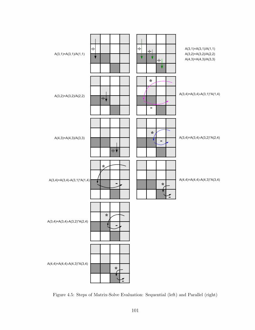
÷ ÷
÷
÷
*
*
*
-
-
-
÷÷
*
-
*
-
*-
A(3,1)=A(3,1)/A(1,1)
A(3,2)=A(3,2)/A(2,2)
A(4,3)=A(4,3)/A(3,3)
A(3,4)=A(3,4)-A(3,1)*A(1,4)
A(3,4)=A(3,4)-A(3,2)*A(2,4)
A(4,4)=A(4,4)-A(4,3)*A(3,4)
A(4,4)=A(4,4)-A(4,3)*A(3,4)
A(3,4)=A(3,4)-A(3,1)*A(1,4)
A(3,1)=A(3,1)/A(1,1)
A(3,2)=A(3,2)/A(2,2)
A(3,4)=A(3,4)-A(3,2)*A(2,4)
A(4,3)=A(4,3)/A(3,3)
Figure 4.5: Steps of Matrix-Solve Evaluation: Sequential (left) and Parallel (right)
101

(a) Dataflow Graph for LU Factorization (Sequential Overlay)
(b) Dataflow Graph for LU Factorization (Wavefront Overlay)
Figure 4.6: Execution Flow for Sparse Matrix-Solve Dataflow Graph
102

ä
x
Depth
Operations Average/Step=75 ops
Matrix-Size=11936%
0 50 100 150 200
300
600
900
(a) Parallelism Profile of psadmit2 benchmark
10%
20%
30%
40%
50%
60%
70%
80%
90%
100%
0 2 4 6 8 10 12 14 16 18 20
% O
pe
ratio
ns
Graph Depth (Bins)
(b) Parallelism Profile of all benchmarks
Figure 4.7: Profiles of Dataflow graphs
nication delays we can estimate peak speedups possible for our benchmark matrices
as shown in Figure 4.8(a). We observe that we can accelerate the matrix solve bench-
marks by 1.45–189×(mean 10.5×) using this ideal parallel hardware. We also show
the predicted utilization of floating-point capacity in Figure 4.8(b). This shows we
can expect mean speedups of 10× and mean utilization of 12% when mapping the
Sparse Matrix-Solve computation to ideal hardware. However, communication la-
tency, poor distribution of processing and queueing delays in the processing element
will limit realizable speedups and floating-point utilization. Additionally, certain rows
and columns in the matrix may be substantially dense (due to high-fanout nets like
power lines, clock, etc) that may create bottlenecks in the compute graph (high-fanin
and high-fanout nodes). In future work, we plan to attack this bottleneck through
associative reduce decomposition.
4.2 Dataflow FPGA Architecture
Our goal is to accelerate the Sparse Matrix Solve computation. This computation
can be represented as a sparse dataflow graph once we have performed symbolic
analysis to lock down non-zero locations. The nodes represent floating-point opera-
tions and edges represent dependencies between the operations as previously shown
in Figure 4.6(b). The sequential microprocessor implementation of this computation
103

1 x
10 x
100 x
bcspwr01
mux8
ringosc
s27psadm
it1
dacpsadm
it2
sandia01
sandia02
s208bcspw
r09
s298s344
s349s444
s386s510
circuit1
s526n
s526s641
10stages
s713circuit2
s820s832
s953ram
2k
bcspwr10
s1196
s1238
s1423
s1494
20stages
circuit3
30stages
mem
plus
40stages
50stages
r4k
Ideal S
peedup
(a) Predicted Speedup of Sparse Matrix-Solve on Ideal Hardware
1 %
10 %
100 %
bcspwr01
mux8
ringosc
s27psadm
it1
dacpsadm
it2
sandia01
sandia02
s208bcspw
r09
s298s344
s349s382
s444s386
s510circuit1
s526n
s526s641
10stages
s713circuit2
s820s832
s953ram
2k
bcspwr10
s1196
s1238
s1423
s1488
s1494
20stages
circuit3
30stages
mem
plus
40stages
50stages
r4k
Ideal F
loating-P
oin
t U
tiliz
ation
(b) Predicted Floating-Point Utilization of Sparse Matrix-Solve on Ideal Hardware (25 PEs)
Figure 4.8: Predicted Performance of Parallel Sparse Matrix-Solve
under-utilizes the floating-point capacity of the processor due to non-floating-point
operations like address calculation and memory fetches (see Figure 4.18(a)). By
extracting the dataflow graph and mapping it to a custom parallel architecture, we
reduce these overheads. We limit the sparse matrix access to local onchip FPGA mem-
ories and implicitly encode instructions in the graph nodes. We expose the inherent
dataflow parallelism available in the computation and route dataflow dependencies
over the packet-switched network.
The Sparse Matrix Solve graph must be evaluated once per SPICE iteration.
Unlike the Model-Evaluation graphs that must be repeatedly evaluated several times
per SPICE iteration in order to process a larger number of identical devices in the
circuit, the sparse matrix graph needs to be processed only once in each iteration.
Hence, we must design an architecture that is optimized for low latency evaluation
of the dataflow graph rather than for high throughput.
The KLU solver provides a static dataflow graph of the matrix factorization. Ide-
ally, we should be able to perform an optimized static schedule of this graph on our
104

PE
PE
PE
PE* + ÷* + ÷
* + ÷* + ÷
Figure 4.9: FPGA Dataflow Architecture for SPICE Sparse-Matrix Solve
Floating-Point *, +,÷
in
out
Data Memory
Graph Memory
Node
DataflowTrigger
Self-Edge
Address
Send Logic
OperandA
Result
OperandB
Dynamically Scheduled
State
Edge
Figure 4.10: PE Organization for SPICE Sparse-Matrix Solve
105

parallel architecture i.e. the scheduler specifies the timing and location of each oper-
ation across the parallel architecture. However, our scheduling infrastructure is too
slow (≈ days of runtime for the largest benchmarks) to handle million-node matrix
factorization graphs. Hence, we use a lightweight, dynamically-scheduled design that
self-times the operations in the dataflow graph. A node in the dataflow graph is
ready for processing when it receives all its inputs. This is the dataflow firing rule.
This technique eliminates the need for static scheduling at the expense of some ad-
ditional area and slightly lower performance. We need to devote additional area to
implement the triggering logic and to support a dynamically-routed packet-switched
network. We sacrifice performance compared to the statically-scheduled design be-
cause we must now make local scheduling and routing decisions with incomplete
information about global system conditions at runtime which may result in longer
latency operation.
Our parallel FPGA architecture contains dataflow-scheduled parallel floating-
point operators coupled to local memories and interconnected by a packet-switched
network (Figure 4.9). This organization is inspired by the Tagged-Token Dataflow
style [97]. This architecture processes dataflow graphs by explicitly passing tokens be-
tween dataflow graph nodes (over the network) and making independent, local firing
decisions to process computation at each node. Each PE processes one dataflow graph
node at a time but manages multiple nodes in the dataflow graph (virtualization) to
handle dataflow graphs much larger than the physical PE count. When the dataflow-
firing rule is satisfied, the floating-point computation at the node is processed by the
PE datapath. The results are then routed to the destination nodes as specified in the
dataflow graph over a packet-switched network using 1-flit packets [59]. Each packet
contains the destination address and the floating-point result.
An FPGA implementation of this computation enables concurrent evaluation of
high-throughput floating-point operations, control-oriented dataflow conditions as
well as pipelined, low-latency on-chip message routing using the same substrate. The
PE shown in Figure 4.9 supports double-precision floating-point add, multiply and
divide and is capable of issuing one floating-point operation per cycle. The network
106

Table 4.1: Parallel Sparse Matrix Solve Studies
Year Ref. Key Idea Hardware PEs Speedup
Parallel Software-based Sparse Matrix Solve for SPICE2000 [98] hybrid iterative, direct SGI Origin 2000 12 3.92005 [99] iterative GMRES - 1 182006 [37] less work; accuracy
tradeoff- 1 7.4
2009 [45] domain decomposition FWGrid 32 119
Parallel FPGA-based Sparse Matrix Solve2004 [100] block decomposition;
fixed-pointAltera EP20K1500FPGA
6 4
2006 [101] block decomposition Xilinx XC2VP125FPGA
35 10
2007 [102] streaming; single-precision
Altera 1S25 FPGA 2 5–6
General-Purpose Parallel Matrix Solve2004 [103] block decomposition Cray T3E 16 4.1
interfaces are streamlined to handle one message per cycle (non-blocking input). We
explicitly store the Matrix-Solve graph structure (shown in Figure 4.6) in local
FPGA on-chip memories. The Dataflow Logic in the PE keeps track of ready nodes
and issues floating-point operations when the nodes have received all inputs (dataflow
firing rule). The Send Logic in the PE inspects network busy state before injecting
messages for nodes that have already been processed. We map the Matrix-Solve
graphs to this architecture by assigning multiple nodes to PEs so as to maximize
locality and minimize network traffic. We route packets between the PEs in packet-
switched manner over a Bidirectional Mesh network. For large graphs, we may not be
able to fit the graph structure entirely on-chip. We can fit the graphs by partitioning
them and then loading the partitions one after another. This is possible since the
graph is completely feed forward (DAGs) and we can identify the order of loads. We
estimate such loading times over a DDR2-500 memory interface.
107

4.3 Related Work
We summarize several recent parallel Sparse Matrix solvers in Table 4.1 and identify
the categories for understanding each design as introduced in Section 2.3.
4.3.1 Parallel Sparse Matrix Solve for SPICE
First, we consider software approaches for parallelizing sparse matrix solvers that are
specific to SPICE circuit simulation. These solvers exploit structural properties of
the SPICE simulation to accelerate the sparse matrix computation. In [98], a hy-
brid direct-iterative solver (Numerical Algorithms) is used to parallelize SPICE
Matrix-Solve phase but requires modifications to the matrix structure (dense row/col-
umn removals) and is able to deliver only 2–3× speedup using 4 SGI R10000 CPUs.
The preconditioned sparse iterative technique GMRES (Numerical Algorithms)
used in [99] is shown to provide 3–18× speedup primarily for circuits dominated by
linear parasitics. It is able to deliver these speedups by reformulating the SPICE
integration and linearization algorithms (SPICE Algorithms). Our technique is
applicable to a broader class of circuits and requires no modification to SPICE al-
gorithms but provides lower speedups. SILCA [37] demonstrates good speedup for
circuits with parasitic couplings by pruning unnecessary work and trading off accu-
racy of the simulation (Precision). Our approach does not sacrifice accuracy and
shows speedups across a large benchmark set. These work-saving techniques can be
adapted for our design to achieve similar benefits.
In [45], a coarse-grained domain-decomposition technique (Numerical Algo-
rithms) is used to achieve 31×-870× (119× geometric mean) speedup for full-chip
transient analysis with 32 processors at SPICE accuracy. The key idea is to decompose
the large circuit matrix into smaller submatrices (domains) using Additive Schwarz
decomposition [45] and then solve the smaller matrices (domains) using a KLU solver.
Our technique accelerates the KLU solve step and can be used in conjunction with
domain-decomposition to accelerate each domain evaluation.
108

4.3.2 Parallel FPGA-based Sparse Matrix Solvers
Next, we review FPGA-based approaches for parallelizing sparse matrix solve com-
putation. FPGA-based accelerators for sparse direct methods have been considered
in [100, 101] and [104, 102] in the context of Power-system simulations. In [100], a
parallel architecture based on embedded processors (Altera NIOS) performs single-
precision LU Factorization (Precision) of symmetric Power-system matrices using
coarse-grained block-diagonal decomposition to deliver a speedup of 4× using 6 NIOS
RISC processor cores (Compute Organization) compared to a uni-processor im-
plementation on a single NIOS core when considering small matrices of size up to
102x102. This comparison does not include the highly-optimized sequential imple-
mentation on an Intel CPU which is likely to be an order of magnitude faster. The
embedded processor requires several cycles to perform network send and receive opera-
tions and cannot spatially implement the non-floating-point operations. Furthermore
it must serialize compute and communicate instructions due to a single instruction is-
sue pipeline. Our processing element design supports double-precision operations and
is streamlined to process an incoming message, an outgoing message and a floating-
point operation per cycle for higher throughput. A different custom architecture
(Compute Organization) implements the block-diagonal decomposition algorithm
(Numerical Algorithm) in [101] but compares performance of a Xilinx XC2VP125
against a TMS320C6711 DSP to demonstrate 10× speedups for small matrices up
to size 32x32. The custom architecture does not use embedded processors like the
NIOS but is still organized as a RISC architecture preventing spatial implementation
of non-floating-point overhead operations.
In [102], a right-looking LU factorization technique using Block-Diagonal decom-
position (Numerical Algorithms) delivers 5–6× speedup for the single-precision
LU Factorization (Precision) using 2 parallel processing units when compared to an
Intel Pentium 4 2.6 GHz for symmetric Power-system matrices. Our approach paral-
lelizes all three phases (LU Factorization, Front-Solve and Back-Solve) on FPGAs in
double-precision arithmetic across 9–25 PEs with faster FPGA hardware (125 MHz vs.
109

200 MHz) and compares performance to the newer Intel Core i7 965. In future work,
we expect to enhance our current FPGA implementation with domain-decomposition
techniques for further accelerating the sparse matrix factorization of asymmetric cir-
cuit matrices.
4.3.3 General-Purpose Parallel Sparse Matrix Solvers
Finally, we briefly discuss techniques used in general-purpose parallel software solvers
for sparse matrices. We report these with the intent of comparing our approach with
non-SPICE-specific parallel sparse solvers and identifying key differences. The par-
allel sparse unsymmetric matrix solver HSL MP48 [103, 105] uses a coarse-grained
strategy to decompose the matrix into diagonal blocks (Numerical Algorithms)
and factors the blocks in parallel using MPI. They report a speedup of 1–9× over 16
processors on a Cray T3E in [103]. While MPI is not directly applicable to tightly-
integrated architectures due to higher latency, we will consider the underlying algo-
rithm in the future to obtain higher speedups. Task queues for scheduling dense
matrix computation (Scheduling) across parallel multi-core architectures are con-
sidered in [106]. This solver organizes processing into DAGs (directed acyclic graphs)
of block operations and uses the task queue to dynamically schedule dependencies be-
tween the block operations to maximize performance. Our FPGA approach performs
sparse LU factorization of matrices whose structure is known a priori and can deter-
mine dependencies between operations on individual matrix entries instead of blocks
for finer-grained parallelism. Scheduling operations at a block-level is unsuitable for
sparse matrices due to the unnecessary sequentialization of possibly concurrent opera-
tions within a block. Our approach exposes all available parallelism in the underlying
sparse matrix dataflow graph without constraining it into blocks. Furthermore, the
communication network between the parallel elements on the FPGA provides a faster
mechanism for moving fine-grained data items across the parallel architecture than
relying on cache-coherency protocols on conventional multi-core processors.
110

Mapping/Placement onFPGA Dataflow Architecture
Parallel Runtime (Cycle-Accurate Simulation)
Spice3f5TransientAnalysis
UFL andPowersystemBenchmarks
KLUSolver Stand-alone
KLU Solver
Matrix-Solve Dataflow Graph
Spice3f5TransientAnalysis
Sparse 1.3Solver
PAPI TimingMeasurement
SequentialRuntime
Figure 4.11: Experimental Flow for Matrix Solve
4.4 Experimental Methodology
We now explain the experimental framework used for the Matrix-Solve design. We
show the entire flow in Figure 4.11. In our experimental flow, we use spice3f5 sim-
ulator with the Sparse 1.3 [17] package for a functional baseline. We integrate the
KLU solver with spice3f5 to replace Sparse 1.3 to measure optimized sequential
performance. For our parallel FPGA design, we measure performance of the dataflow
graph extracted from the KLU [15] solver using a cycle-accurate simulator that mod-
els the dataflow architecture. We compare the sequential and parallel implementation
across a range of benchmark matrices generated from spice3f5, circuit-simulation
matrices from the University of Florida Sparse-Matrix Collection [111] as well as
Power-system matrices from the Harwell-Boeing Matrix-Market Suite [112]. For ma-
trices generated from spicef5, we use circuit benchmarks provided by Simucad [107],
Igor Markov [108], Paul Teehan [109] and Sani Nassif [110]. Our benchmark set cap-
tures matrices from a broad range of problems that have widely differing structure.
We tabulate key characteristics of these benchmarks in Table 4.2 and Table 4.3.
111

Bmarks. MatrixSize
Sparsity(%)
Mult.Sub.
Divide TotalOps.
Fanout(DFG)
Fanin(NZ)
Latency(cycles)
spice3f5, Simucad [107]mux8 42 15.0793 488 138 626 8 20 1.9Kringosc 104 6.4903 1.3K 351 1.6K 4 92 3.7Kdac 654 1.5849 20.2K 3.3K 23.6K 10 1136 7.7Kram2k 4875 0.3107 1.0M 38.5K 1.0M 137 9618 62.2K
spice3f5, Clocktrees [108]r4k1 39948 0.0131 390.3K 125.1K 515.5K 6 29910 127.8K
spice3f5, Wave-pipelined Interconnect [109]10stages 3920 0.1753 57.8K 14.8K 72.7K 8 2384 18.6K20stages 11225 0.0618 174.8K 44.4K 219.2K 9 9442 46.2K30stages 16815 0.0410 244.3K 61.7K 306.0K 11 4688 88.6K40stages 22405 0.0307 316.1K 79.5K 395.7K 9 600 134.2K50stages 27995 0.0245 394.7K 99.2K 493.9K 10 484 169.7K
spice3f5, ISCAS98 Netlists [110]s27 189 3.4405 2.1K 573 2.7K 6 50 3.6Ks208 1296 0.5277 19.7K 4.9K 24.6K 11 1414 11.3Ks298 1801 0.4026 32.6K 7.3K 40.0K 13 1938 13.1Ks344 1992 0.3522 32.3K 7.8K 40.1K 12 2178 14.7Ks349 2017 0.3512 33.9K 8.0K 41.9K 14 2218 14.7Ks382 2219 0.3184 37.2K 8.7K 45.9K 16 2358 16.1Ks444 2409 0.2952 41.4K 9.6K 51.1K 16 2526 16.6Ks386 2487 0.2927 46.4K 10.0K 56.5K 20 2626 15.7Ks510 2621 0.3124 105.3K 11.9K 117.2K 54 2722 21.4Ks526n 3154 0.2362 66.1K 13.0K 79.2K 25 3280 21.9Ks526 3159 0.2376 68.1K 13.3K 81.4K 26 3294 20.7Ks641 3740 0.2000 100.2K 15.6K 115.9K 39 4066 26.5Ks713 4040 0.1890 126.4K 17.1K 143.5K 47 4380 30.3Ks820 4625 0.1655 103.2K 19.6K 122.8K 29 4766 26.1Ks832 4715 0.1629 105.7K 20.0K 125.8K 29 4846 26.6Ks953 4872 0.1876 353.9K 24.3K 378.2K 85 5212 37.9Ks1196 6604 0.1399 475.3K 33.0K 508.3K 83 7146 46.4Ks1238 6899 0.1325 457.9K 34.2K 492.2K 78 7454 46.6Ks1423 9304 0.0820 296.0K 39.4K 335.4K 64 10384 64.5Ks1488 9849 0.0827 354.7K 44.7K 399.4K 49 10606 54.8Ks1494 9919 0.0817 352.4K 44.8K 397.3K 50 10646 54.6K
Table 4.2: Circuit Simulation Benchmark Matrices
112

Bmarks. MatrixSize
Sparsity(%)
Mult.Sub.
Divide TotalOps.
Fanout(DFG)
Fanin(NZ)
Latency(cycles)
Circuit Simulation, UFL Sparse Matrix [111]
sandia01 1220 0.6348 19.1K 4.2K 23.3K 8 70 5.7Ksandia02 1220 0.6348 19.1K 4.2K 23.3K 8 70 5.7Kcircuit1 2624 0.6127 408.0K 22.3K 430.3K 82 5092 36.2Kcircuit2 4510 0.1563 202.9K 16.1K 219.0K 172 2538 23.3Kcircuit3 12127 0.0463 160.6K 37.8K 198.4K 21 9008 48.7Kmemplus 17758 0.0400 798.8K 71.9K 870.8K 97 956 27.6K
Power-system, Matrix Market [112]
bcspwr01 39 12.9520 335 114 449 6 14 2.6Kpsadmit1 494 0.9564 4.3K 1.4K 5.7K 10 46 4.9Kpsadmit2 1138 0.4163 9.8K 3.2K 13.0K 11 62 6.7K
Table 4.3: UFL Matrix Circuit-Simulation Benchmarks
Block Area Latency DSP48 BRAM Speed Ref.(Slices) (clocks) (blocks) (min.) (MHz)
Add 334 8 0 0 344 [77]Multiply 131 10 11 0 294 [77]Divide 1606 57 0 0 277 [77]
Processing Element 2368 - 11 8 270 -Mesh Switchbox 642 4 0 0 312 -DDR2 Controller 1892 - 0 0 250 [88]
Table 4.4: Area and Latency model for Sparse Matrix-Solve Hardware (Virtex-6 LX760)
Our parallel FPGA architecture handles dataflow graphs of the sizes shown in
column ‘Total Ops.’ of Table 4.2 and Table 4.3. We generate the dataflow graphs for
LU factorization as well as Front/Back solve steps from the initial symbolic analysis
and reordering phase of the KLU solver. Once we have the dataflow graphs, we assign
nodes to PEs of our parallel architecture. We consider two strategies for placing
nodes on the PEs: random placement and placement for locality using MLPart [73]
with fanout decomposition. We will consider additional strategies for distributing
the graph nodes across our parallel dataflow architecture for higher performance as
future work.
113

4.4.1 FPGA Implementation
We consider a single-chip design of our dataflow architecture on a Xilinx Virtex-5
SX95T and a Xilinx Virtex-6 LX 760 FPGAs. We allow the dataflow design to use
the complete FPGA area for these experiments, but when composing the complete
SPICE design, we partition the FPGA accordingly (see Chapter 6). In some cases,
the dataflow graph will not fit entirely in the FPGA onchip memories. As identified
earlier, we can statically compute a loading order and stream the dataflow graph from
an offchip DRAM memory.
For our PE design, we use spatial implementations of individual floating-point
add, multiply and divide operators from the Xilinx Floating-Point library in Core-
Gen [77]. These implementations do not support denormalized (subnormal) num-
bers. We compose the two-dimensional, packet-switched network organized as an
84-bit Bidirectional Mesh (64-bit data, 20-bit address). Each switch in the network
is assembled using simple split and merge blocks as described in [59]. The switches
implement Dimension-Ordered Routing (DOR [113]). We pipeline the wires between
the switches for high performance. Every Manhattan hop in the mesh takes 9 cycles
including switch and wire pipeline delays. We estimate memory load time for large
matrices using streaming loads over the external DDR2-500 MHz memory interface
using lowerbound bandwidth calculations. We do not require a detailed cycle-accurate
simulation for the memory controller since it is a simple, sequential, streaming ac-
cess pattern that we know and precompute. We show the area and latency model in
Table 4.4.
We synthesize and implement a sample double-precision 4-PE design on a Xilinx
Virtex-5 device using Xilinx ISE 12.1. We provide placement and timing constraints
to the backend tools and attain a frequency of 250 MHz. We can fit a system of 9
PEs on a Virtex-5 SX240T (77% logic occupancy) while systems with 25 PEs are
easily possible on a Virtex-6 LX760 (estimated 65% logic occupancy). We note that
our architecture is frequency limited primarily by the Xilinx floating-point divide
operator and the DDR2 controller bandwidth. We can improve our clock frequency
114

1e-16
1e-14
1e-12
1e-10
1e-8
1e-6
ringosc
ram2k
mux8
dac10stages
r10k1
s27s208
s298s344
s349s382
s386s444
s510s526
s526n
s641s713
s820s832
s953s1196
s1238
sandia01
sandia02
psadmit1
psadmit2
bcspwr01
circuit1
circuit2
circuit3
Re
sid
ue
(b
-Ax)
Matrices
bicgstab gmres klu
Figure 4.12: Comparing Iterative Solvers with KLU
further by using better division algorithms (e.g. SRT-8) and better memory interfaces
(e.g. DDR3) for additional external memory bandwidth.
4.5 Results
We now discuss experimental results for parallelizing the Sparse Matrix Solve phase
of SPICE. We first show results for some initial exploratory studies that attempted
to use Iterative algorithms but were not robust enough for circuit simulation. Next,
we look at the performance of the sequential SPICE solver with the KLU solver
integrated into the package. Finally, we present detailed analysis of the performance
of our FPGA design and identify the underlying factors to explain our results.
4.5.1 Exploring Opportunity for Iterative Solvers
It is well-known that iterative algorithms for Sparse Matrix Solve based on Krylov-
subspace techniques can be parallelized more effectively [93]. In contrast with direct
solvers that perform an LU decomposition, the iterative algorithms use repeat evalu-
ations of Sparse Matrix-Vector multiplications. These Matrix-Vector multiplications
can be parallelized very effectively on FPGAs [114], GPUs [115] and even Multi-
Cores [87]. Sparse direct solvers are not as easy to parallelize and require additional
effort. However, iterative techniques are not always sufficiently robust across different
115

application scenarios. A lack of robustness may result in SPICE simulations that do
not converge at all or converge too slowly. It is possible to improve the robustness
of these iterative solvers using preconditioning. We experimented with a range of
preconditioned iterative algorithms and sparse direct solvers to evaluate their effec-
tiveness for solving circuit simulation matrices. We show the residues (~b− A~x) from
our experiments in Figure 4.12. The smaller the residue the better the result. We
observe that the KLU solver and the preconditioned-BiCG solvers deliver the most
robust results across our benchmark set. The preconditioned-GMRES algorithm is
consistently generating poor solutions with high residues in a majority of the cases.
While preconditioned BiCG iterative algorithm does deliver reasonable results, the
cost of calculating the incomplete LU preconditioner (using a sparse, direct method)
is expected to be comparable to the cost of complete LU factorization using a sparse
direct method. This initial exploration suggested that we will need to parallelize
the sparse direct solver in any case. For the purpose of this thesis, we focus on
parallelizing the KLU sparse direct solver. In future work, we will fully explore the
opportunities for using a parallel preconditioned iterative solver for SPICE.
4.5.2 Sequential Baseline: KLU with spice3f5
For our experiments, we first compare the sequential performance of the KLU solver
with the Sparse 1.3 solver (default in spice3f5). We replace the Sparse 1.3 solver
with the newer, improved KLU solver for all transient iterations. Note that both
techniques use the exact same convergence conditions defined in spice3f5 without
any loss in accuracy nor an increase in Newton-Raphson iterations. For simplicity,
we currently retain Sparse 1.3 to produce the DC operating point at the beginning
of the simulation. We quantify the performance benefits of using the newer solver by
measuring the runtimes of Matrix-Solve phase of spice3f5 with PAPI 4.0.0 [18]
performance counters. We measure runtimes of these sequential solvers when using
a single core of the Intel Core i7 965 processor. We compute speedup for the KLU
implementation using the formula in Figure 4.13.
We show the speedup for using the KLU solver over the Sparse 1.3 solver in
116

Software Speedup =Tsparse1.3(refactor) + Tsparse1.3(front solve) + Tsparse1.3(back solve)
Tklu(refactor) + Tklu(front solve) + Tklu(back solve)
Tsparse1.3(refactor) = Sparse 1.3 Solver LU Refactorization Time on CPU
Tsparse1.3(front solve) = Sparse 1.3 Solver Front-Solve Time on CPU
Tsparse1.3(back solve) = Sparse 1.3 Solver Front-Solve Time on CPU
Tklu(refactor) = KLU Solver LU Refactorization Time on CPU
Tklu(front solve) = KLU Solver Front-Solve Time on CPU
Tklu(back solve) = KLU Solver Front-Solve Time on CPU
FPGA Speedup =Tklu(refactor) + Tklu(front solve) + Tklu(back solve)
Tfpga(refactor) + Tfpga(front solve) + Tfpga(back solve)
Tfpga(refactor) = KLU Solver LU Refactorization Time on FPGA
Tfpga(front solve) = KLU Solver Front-Solve Time on FPGA
Tfpga(back solve) = KLU Solver Front-Solve Time on FPGA
Figure 4.13: Speedup Calculation Equation for Sparse Matrix-Solve Implementations
0
1
2
3
4
5
s27m
ux8
ringosc
s208s298
s344s349
dacs400
s444s386
s510s526n
s52610stages
s641s713
s953s820
s832s1196
s1238
s1423
20stages
s1494
30stages
40stages
50stages
ram2k
r4k
KLU
Speedup
1.35x mean
Figure 4.14: Sequential Sparse Matrix-Solve Speedup for KLU over Sparse 1.3(Intel Core i7 965)
117

Tseq(klu analayze)
Tpar(klu total)=
5 · Tseq(klu iter)104 · Tpar(klu iter)
=50 · Tpar(klu iter)104 · Tpar(klu iter)
= 0.5%
Figure 4.15: KLU Analysis Overhead of Parallel KLU Runtime(104 iterations, 10×speedup)
sequential spice3f5 in Figure 4.14. We show additional details in Table 4.5 where
we include runtimes for the different components of Sparse Matrix-Solve phase when
using the Sparse 1.3 solver and the KLU solver. We see that KLU improves the per-
iteration matrix solve time by as much as 4.6× for the largest ram2k benchmark while
delivering a geometric mean improvement of 1.35× on the whole benchmark set. We
also observe that, for some matrices, KLU delivers similar performance as Sparse 1.3
(e.g. 10stages, s298). For very small matrices ≤ 200 rows (e.g. mux8, s27, ringosc),
the KLU solver actually slows down the Matrix-Solve phase by ≈50%. The symbolic
analysis time (sub-column Analyze in column KLU) is ≈5× the runtime of a single
KLU Matrix-Solve iteration. This means that even if the analysis phase remains
sequentialized and we speedup iterations by 10× (see Figure 4.16), analysis accounts
for only 0.5% of total runtime after 10K iterations (3.3K timesteps for an average
of 3 iterations/timestep seen in our benchmark set). We show this calculation in
Equation 4.15. We use this faster KLU solver as the sequential baseline for computing
speedups of our FPGA architecture.
4.5.3 Parallel FPGA Speedups
For our Dataflow FPGA implementation we compute speedup using the formula pre-
viously described in Figure 4.13. In Figure 4.16, we show the speedup of our FPGA
architecture using the best placed design that fits in the FPGA over the sequential
software version running on an Intel Core i7 965. We obtain speedups between 0.6–
7.1×(geomean 2.4×) for Virtex-6 LX760. We observe a slight slowdown for very small
matrices mux8 and ringosc. We deliver a speedup of 1.5–5.8× (geomean 3.4×) for
Power-system simulation matrices accelerated using FPGAs in [101]. Our solution
is 2× faster than the one presented in [101] (estimated from MFLOPs since straight
118

Benchmark Sparse 1.3 (ms) KLU (ms) Ratio AnalyzeLU Solve Total Analyze LU Solve Total (#Iters.)
s27 0.02 0.00 0.03 0.21 0.04 0.01 0.05 0.60 4mux8 0.00 0.00 0.00 0.05 0.00 0.00 0.01 0.65 5ringosc 0.01 0.00 0.01 0.12 0.01 0.00 0.02 0.66 5s208 0.23 0.10 0.33 1.35 0.25 0.07 0.33 0.99 5s298 0.43 0.17 0.60 2.12 0.43 0.12 0.55 1.10 4s344 0.45 0.18 0.63 2.09 0.45 0.12 0.57 1.10 4s349 0.48 0.22 0.71 2.15 0.46 0.12 0.59 1.20 4dac 0.14 0.05 0.20 0.56 0.17 0.04 0.21 0.93 3s400 0.51 0.20 0.71 0.00 0.51 0.20 0.71 1.00 0s444 0.54 0.22 0.77 2.71 0.50 0.13 0.63 1.20 5s386 0.65 0.24 0.90 3.09 0.60 0.16 0.77 1.16 5s510 1.12 0.29 1.41 3.47 0.82 0.17 0.99 1.42 4s526n 0.97 0.32 1.29 3.95 0.83 0.21 1.04 1.23 4s526 0.97 0.33 1.31 3.98 0.84 0.21 1.05 1.24 410stages 0.40 0.17 0.57 4.31 0.41 0.11 0.53 1.09 9s641 1.07 0.36 1.44 4.24 0.90 0.21 1.12 1.28 4s713 1.50 0.47 1.97 4.69 1.16 0.26 1.42 1.38 4s953 4.15 0.67 4.82 6.84 2.06 0.34 2.41 1.99 3s820 1.48 0.50 1.98 6.91 1.21 0.30 1.52 1.30 5s832 1.50 0.51 2.01 7.16 1.22 0.31 1.54 1.30 5s1196 6.58 0.95 7.54 9.47 2.83 0.48 3.31 2.27 3s1238 6.04 0.97 7.02 9.95 2.75 0.49 3.24 2.16 4s1423 4.11 1.13 5.24 12.08 2.77 0.57 3.35 1.56 420stages 1.93 0.72 2.65 14.07 1.51 0.38 1.90 1.39 8s1494 6.68 1.35 8.03 18.72 3.37 0.66 4.03 1.99 530stages 3.35 1.12 4.48 22.67 2.29 0.57 2.87 1.56 840stages 5.12 2.05 7.18 31.37 3.06 0.78 3.85 1.86 950stages 7.47 3.33 10.80 40.44 4.04 1.02 5.06 2.13 8ram2k 22.96 1.36 24.32 15.79 4.89 0.38 5.28 4.60 3r4k 16.50 9.06 25.57 42.48 8.99 2.45 11.44 2.23 4
Geometric Mean 1.35 5
Table 4.5: Runtime Per Iteration of KLU and Sparse 1.3
119

0 x
1 x
10 x
bcspwr01
mux8
ringosc
s27psadm
it1
dacpsadm
it2
sandia01
sandia02
s208bcspw
r09
s298s344
s349s444
s386s510
circuit1
s526s641
10stages
s713circuit2
s820s832
s953s1196
s1238
s1423
s1494
20stages
circuit3
30stages
mem
plus
40stages
50stages
r4k
Speedup
3.8x
2.4x
mean(ideal)mean(pessimistic)
ideal (overlap mem.)pessimistic (sequential mem.)
Figure 4.16: FPGA Speedups for Sparse Matrix-Solve for Circuits and UFL Matrices(Virtex-6 LX760 vs. Intel Core i7 965)
0.1%
1.0%
10.0%
bcspwr01
s27psadm
it1
dacpsadm
it2
sandia01
sandia02
s208bcspw
r09
s298s344
s349s444
s386s510
circuit1
s526s641
10stages
s713circuit2
s820s832
s953s1196
s1238
s1423
s1494
20stages
circuit3
30stages
mem
plus
40stages
50stages
r4k
% o
f F
loating-P
oin
t P
eak
4.5%
2.2%
mean(fpga)mean(cpu)
fpga (25 PEs)cpu (1 core)
Figure 4.17: Achieved Floating-Point Peaks
120

runtime figures were not reported) due to independent processing of routing and
floating-point operations. For these speedup calculations we include memory loading
time for the large dataflow graph from external DRAM. We also compute speedups
in the case where we can overlap memory loading with computation. This is possible
since the graph is entirely feed-forward and we can compute a load order in advance.
Under this optimistic assumption we can achieve speedups between 0.64–13.49× (ge-
omean 3.8×). We also wish to explore the opportunity for placing large dataflow
graphs using greedy packers to avoid the bad random distributions as part of our
future work.
In Figure 4.17, we show the percent of peak floating-point throughput of our 25-
PE Virtex-6 LX760 FPGA design as well as 1 core of the Intel Core i7 965 processor.
A multi-core implementation for the KLU solver currently does not exist. Our exper-
iments with exposing the dataflow structure directly to the multi-core architecture
resulted in poor performance. Hence, for this study, we limit our comparisons to the
1-core implementation. The peak double-precision floating-point throughput of our
25-PE design is 12.5 GFLOPs while that of 1 core of the Intel Core i7 965 is 6.25
GFLOPs. We see that the FPGA is able to achieve a geometric mean 4.5% of the
floating-point peak of the FPGA while the CPU can only achieve 2.2% of its peak.
This translates into 33–1104 MFLOPS (geomean of 520 MFLOPS) on the 25-PE
while the processor is only able to achieve rates of 21-502 MFLOPS (geomean of 137
MFLOPS). The FPGA mean speedups and floating-point utilization are within 2–3×
of their predicted values shown earlier in Figure 4.8. This indicates we need to explore
different parallelization strategies such as domain decomposition on top of the sparse
dataflow parallelism for further accelerating the Sparse Matrix-Solve phase of SPICE.
4.5.4 Limits to Parallel Performance
We now attempt to provide an understanding of sequential and parallel performance
and identify opportunities for improvement.
We measure the dynamic instruction distribution in the Intel Core i7 implemen-
tation of computation in Figure 4.18(a). We observe that only of 1.3% (geomean) of
121

total instructions are actually floating-point instructions. This partly explains why
we observe poor actual floating-point performance in Figure 4.17. The non-floating-
point instructions are devoted to address-calculation and memory fetch operations
on the sparse matrix data-structures. We can see in Line 9 from Listing 4.2 that we
must perform 3 reads and 1 write for each execution of that statement which may
require several cycles if not in the cache. Furthermore, we must lookup the non-zero
location corresponding to the j, ith entry in the matrix L through an address table
which can, in turn, take multiple cycles.
Our FPGA implementation achieves a higher utilization and delivers speedup by
spatially distributing these address-calculation overheads and by directly routing mes-
sages between graph nodes where needed. Next, we measure runtimes of the different
phases of the FPGA implementation in Figure 4.18(b) to identify bottlenecks. This
shows that memory loading times can account for as much as 38% of total runtime
while the LU-factorization phase can account for as much as 30%. Memory load
times (limited by DRAM bandwidth) can be reduced by around 3–4× using a higher-
bandwidth DRAM interface (saturating all FPGA IO and using DDR3-800) while the
LU-factorization runtime can be improved in a limited fashion with better placement
of graph nodes.
In Figure 4.18(c), we attempt to bound the additional improvement that may
be possible in runtime for the dominant phase: LU factorization. For these esti-
mates we ignore communication bottlenecks. We first compute the latency of the
critical path of floating-point instructions in the compute graph. This critical path
latency (Tcritical) is the ideal latency that can be achieved assuming infinite PEs,
unlimited DRAM bandwidth and no routing delays. This provides an upper bound
on achievable speedup (Speeduplatency = Tsequential/Tcritical). When we account for
serialization in each PE arising from reuse of PE resources, we can compute another
upper-bound on achievable performance. The floating-point operators in each PE
must be shared by multiple dataflow graph nodes. Next, we consider IO serialization
latency (Tserialization) which measures the number of cycles required to send and receive
messages into the network. We compute another idealized (approximate) estimate of
122

1.0%
10.0%
bcspwr01
mux8
ringosc
s27psadm
it1
dacpsadm
it2
sandia02
sandia01
s208bcspw
r09
s298s344
s349s382
s444s386
s510circuit1
s526n
s526s641
10stages
s713circuit2
s820s832
s953ram
2k
bcspwr10
s1196
s1238
s1423
s1488
s1494
20stages
circuit3
30stages
mem
plus
40stages
50stages
r4k
Flo
atin
g-P
oin
t In
str
. (%
)
1.3% mean
(a) Floating-Point Fraction of Total Instructions for CPU
0 10 20 30 40 50 60 70 80 90
100
bcspwr01
mux8
ringosc
s27psadm
it1
dacpsadm
it2
sandia01
sandia02
s208bcspw
r09
s298s344
s349s382
s444s386
s510circuit1
s526s641
10stages
s713circuit2
s820s832
s953s1196
s1238
s1423
s1488
s1494
20stages
circuit3
30stages
mem
plus
40stages
50stages
r4k
Ru
ntim
e/I
tera
tio
n (
ms)
LU Factorization Front-Solve Back-Solve Memory Load
(b) Runtime Distribution of Parallel FPGA Time (25-PE Virtex-6 LX760)
1 x
10 x
bcspwr01
mux8
ringosc
s27psadm
it1
dacpsadm
it2
sandia01
sandia02
s208bcspw
r09
s298s344
s349s382
s444s386
s510circuit1
s526s641
10stages
s713circuit2
s820s832
s953s1196
s1238
s1423
s1488
s1494
20stages
circuit3
30stages
mem
plus
Ad
ditio
na
l S
pe
ed
up
Bo
un
d
2.5x
(c) Additional Speedup Possible (Critical Path and Serialization Bounds)
Figure 4.18: Understanding FPGA Sparse Matrix-Solve Performance
123

0
2
4
6
8
10
12
14
1 2 3 4 5 6 0
2
4
6
8
10
12
14
Rela
tive S
peedup
Mesh Side Length
geomean
Figure 4.19: Impact of Scaling PE Count (PE=Mesh Side*Mesh Side)Each color represents a matrix in our benchmark set
these serialization overheads at 25 PEs to get a tighter bound on achievable speedup
(Speedupserialization = Tsequential/Tserialization). The estimated speedup is the lower
of the two idealized estimates (Speedup = MIN(Speeduplatency, Speedupserialization)).
For most of our benchmarks we are within a 2× of the ideal latency scenario. This
suggests that a limited amount of additional speedup is achievable for such bench-
marks using better distribution and placement of sparse dataflow parallelism. For
larger benchmarks such as s1196, memplus higher additional speedups are possible.
For netlists with high potential speedups, we are currently unable to contain the crit-
ical paths effectively into few PEs. We expect to extract higher performance for large
sparse dataflow graphs through novel placement and clustering strategies as part of
our future work.
4.5.5 Impact of Scaling
In Figure 4.19, we show the impact of scaling system size (PE count) on performance.
We observe a wide range of scaling trends ranging from 14× speedup at 36 PEs
(requires 2 Virtex-6 LX760 FPGAs) to no speedups at all in some cases (in fact
some slowdown). Large netlists like 40stages, 50stages which are relevant and
challenging for parallelization show the best scaling. These netlists have low fanout
124

1 x
10 x
bcspwr01
mux8
ringosc
s27psadm
it1
dacpsadm
it2
sandia02
sandia01
s208bcspw
r09
s298s344
s349s444
s386s510
circuit1
s526s641
10stages
s713circuit2
s820s832
s953s1196
s1238
s1423
s1494
20stages
circuit3
30stages
mem
plus
40stages
50stages
Sp
ee
du
p
4.7x
2.9x2.4x
high-bandwidth IO low-latency FP original
Figure 4.20: Speculative Speedups(1) Low-Latency Operators (2) High-Bandwidth Offchip IO
8–10 and modest fanin within a column ≈400-9000. Small netlists like mux8, ringosc
and bcspwr01 show poor scaling due to the small dataflow graph sizes ≈600–2000. We
see mean speedup scaling saturates at around 4× at 16 PEs with modest improvement
to 5× at 36 PEs. This modest speedup scaling is primarily due to the long tail of
the dataflow graph. We saw in Figure 4.7 that bulk of the nodes in the graph have
a depth of 1–2 in the graph. We also saw in Figure 4.18(c) that for most matrices
we are only ≈2× away from ideal critical-path latency in the dataflow graph. This
suggests we must investigate alternate strategies for exploiting parallelism. We may
be able to improve the latency of the packet-switched network (currently 9 cycles per
Manhattan hop) with an alternate design. We discuss a few of our ideas for future
work in Chapter 8.
In Figure 4.20, we estimate the impact of two architecture changes on final
speedups. We first reduce the latency of the floating-point operations to 1 cycle per
operation to minimize the impact of operator latency on total performance. Then, we
increase offchip IO bandwidth available on the FPGA by 10× to reduce memory load
times. We observe that reducing operator latency improves performance marginally
from 2.4× to 2.9×. This suggests that a significant portion of the total cycles is due
to packet-switched interconnect. In future work, we must also consider lower latency
network designs to improve performance. We also observe a higher improvement in
performance from 2.4× to 4.7× when we increase offchip IO bandwidth.
125

4.6 Conclusions
In this chapter, we show how to implement the irregular Sparse Matrix-Solve phase of
SPICE on an FPGA for a range of matrix and circuit benchmarks. We demonstrate
speedups of 0.6–13.4×when comparing a 25-PE parallel implementation on a Xilinx
Virtex-6 LX760 FPGA with a 1-core implementation on an Intel Core i7 965 for
double-precision floating-point evaluation. Our token dataflow FPGA architecture
permits lightweight distributed processing of the sparse, irregular factorization graph
to deliver better performance. At present, our speedups for the Sparse Matrix-Solve
phase are limited primarily due to limited parallelism in the sparse dataflow graph.
Additionally, we are also affected by a combination of factors including memory load
times, long latency floating-point operations and poor distribution of critical path
across the parallel elements.
In future work, we will investigate different numerical algorithms (e.g. iterative,
domain-decomposition) to explore a different strategy to exploit higher parallelism
than that available in the sparse dataflow graph. In the short term, we expect to
improve FPGA speedups in the future using better placement algorithms that op-
timize latency of evaluation, overlapped streaming fetch from offchip-memory, and
lower latency floating-point operators [91, 92]. We will also develop vector implemen-
tations of the levelized dataflow graphs to compare performance against GPUs and
Intel multi-core CPUs.
126

Chapter 5
Iteration Control
In Chapter 3 and 4, we discussed the two computationally-intensive phases of the
SPICE simulator. In this chapter, we explain how to implement the sequential,
control-intensive SPICE state-machines. We also discuss a streaming approach that
will permit a high-level expression of the Iteration Control computation using the
SCORE [10] framework. We show that ignoring this phase for parallelization results
in mean speedups of 2.4× for the composed SPICE simulator. We caution against
mapping this sequential Iteration Control computation to a lightweight embedded mi-
crocontroller (e.g. Microblaze) as it creates a performance bottleneck and decreases
overall speedups to 1.9×. We discuss our FPGA organization that uses a combina-
tion of static and dynamic scheduling to deliver balanced speedups of 2.6× for the
integrated design.
5.1 Structure in Iteration Control Phase
As discussed in Chapter 2, SPICE is an iterative algorithm that solves non-linear
differential equations. SPICE solves these equations using an iterative approach that
first linearizes the non-linear circuit elements and then performs a numerical integra-
tion involving time-varying quantities. The space of algorithms for linearization and
numerical integration is vast, and it covers conflicting requirements of convergence
speed, accuracy and stability while demanding different amounts of computation and
memory storage costs. The choice of a suitable algorithm applicable to circuit sim-
127

Convergence Condition
Vectors V, I, f
SPICEIteration
Non-Linear Converged?
Increment timestep?
Transient Iterations
Newton-Raphson Iterations
Vectors Qi, Qi-1
LocalTruncation
Error (LTE)
converged timestep
BreakpointLogic
Iteration Control
ba
AnalysisState-Machines
c
d
2
1
Figure 5.1: Flowchart of a SPICE Simulator with emphasis on SPICE Analysis ControlAlgorithms
ulation is the subject of continued research and is beyond the scope of this thesis.
Using the framework and methodology described in this chapter, we can support
newer algorithms for managing the SPICE simulation. For the purpose of this the-
sis and as a proof-of-concept, we pick the algorithms used in the spice3f5 package:
the Newton-Raphson algorithm for handling non-linear elements and the Trapozoidal
approximation for numerical integration.
The spice3f5 iteration controller manages two kinds of iterative loops: 1© a loop
for linearizing the non-linear elements of the circuit, and 2© another loop for advancing
the timestep of the simulation. We show these loops in Figure 5.1. The convergence
conditions for the Newton-Raphson algorithm are implemented in the block a© of
the figure. SPICE employs the Newton-Raphson algorithm for computing the linear
operating points of non-linear devices like diodes and transistors. The equation for
next timestep calculation is implemented in block b© of the figure. SPICE uses an
adaptive timestep-control algorithm that adjusts the timestep of the simulation based
on an estimate of local truncation error as previously introduced in Section 2.1.3. In
128

block c©, SPICE implements the dynamic breakpoint processing logic for handling
source transition timesteps in the voltage and current sources. Finally, in block d©,
the analysis state machines implement the loop control algorithms for performing
DC and transient analysis. The Iteration Control computation constitutes a small
(7%) fraction of total SPICE runtime. We reported these measurements earlier in
Figure 2.9 shown in Section 2.2.
5.2 Performance Analysis
We now show the benefit of carefully parallelizing the Iteration Control phase of
SPICE. In Figure 5.2 we show the runtimes of the different phases of SPICE with
and without parallelization for the s641 and r4k SPICE netlists. In the “Sequential”
column we observe that sequential runtime is dominated by the Model-Evaluation
computation and the Iteration Control is a small 7–8% fraction of total runtime.
When we parallelize the Model-Evaluation and the Sparse Matrix-Solve phases on
a Virtex-6 LX760, we notice that the Iteration Control is now a significant 24–50%
portion of total runtime (see Column “Ignore IterCtrl”). This is especially true for
the r4k SPICE netlist where it is 50% of total runtime. This suggests, that we must
parallelize this phase to achieve high overall speedup. This is very relevant as we
scale to larger FPGA sizes in the future. In that case, since we have more area at our
disposal, we can further parallelize the Model-Evaluation and Sparse Matrix-Solve
phases of SPICE. The sequential Iteration Control phase will be an even greater frac-
tion of parallel runtime. In column “Spatial IterCtrl” we show the effect of spatially
parallelizing the Iteration Control phase on total performance. Like other FPGA
designs [116], we may choose to implement the Iteration Control portion on an em-
bedded processor e.g. Microblaze. However, in Column “Microblaze IterCtrl” for the
s641 netlist, we observe that this is a poor implementation choice and results in lost
speedup. We discuss performance comparison in greater detail in Section 5.6. These
two distributions suggest that we must avoid a sequential Microblaze implementation
of the Iteration Control phase while parallelizing this phase properly.
129

0 0.2 0.4 0.6 0.8
1 1.2 1.4 1.6 1.8
2
Sequential IgnoreIterCtrl
SpatialIterCtrl
MicroblazeIterCtrl
Ru
ntim
e/I
tera
tio
n
(mill
ise
co
nd
s)
Iteration ControlModel-Evaluation
Matrix-Solve
(a) Runtimes for s641 netlist
0
5
10
15
20
25
30
35
40
Sequential IgnoreIterCtrl
SpatialIterCtrl
MicroblazeIterCtrl
Ru
ntim
e/I
tera
tio
n
(mill
ise
co
nd
s)
Iteration ControlModel-Evaluation
Matrix-Solve
(b) Runtimes for r4k netlist
Figure 5.2: Runtime Distribution for SPICE Phases (Virtex-6 LX760 ParallelImplementation)
0
20
40
60
80
100
102
103
104
105
Perc
ent of T
ota
l R
untim
e
Circuit Size
61%
26%
7%
Modeleval.Modeleval.(avg)
Matsolve.
Matsolve.(avg)Iterctrl.
Iterctrl, (avg)
(a) Sequential Percent Distribution
0
20
40
60
80
100
102
103
104
105
Perc
ent of T
ota
l R
untim
e
Circuit Size
38%
42%
19%
Modeleval.Modeleval.(avg)
Matsolve.
Matsolve.(avg)Iterctrl.
Iterctrl.(avg)
(b) Parallel Percent Distribution (Seq. IterCtrl)
Figure 5.3: Sequential and Parallel Performance Fractions of spice3f5 (Virtex-6 LX760Parallel Implementation)
We present another way to look at the performance of Iteration Control in Fig-
ure 5.3. We compare the contribution of the Iteration Control phase of SPICE before
(Figure 5.3(a)) and after (Figure 5.3(b)) parallelizing the other two SPICE phases.
We observe that once the rest of SPICE is parallelized, the contribution of the Iter-
ation Control phase increases from 7% to 19% of total parallel runtime. Hence it is
important to seek ways to extract parallelism out of this phase of SPICE to deliver
overall speedups.
What will happen to overall speedups if we do not parallelize Iteration Control?
In Figure 5.4, we see that a speculative 25× speedup for the Model-Evaluation and
130

1
2
4
8
16
32
s298
s344
s349
s382
dac
s444
s386
s510
s526
10sta
ges
s641
s713
s953
s820
s832
s1196
s1238
s1423
20sta
ges
s1494
30sta
ges
40sta
ges
50sta
ges
r4k
Speedup
25x Speedup for Rest (Hypothetical Chip)
Figure 5.4: Performance Bound on Parallelizing spice3f5 by ignoring Iteration Control
Sparse Matrix-Solve phase of SPICE results in an overall speedup of only ≈9×. This
is due to Amdahl’s Law (shown in Equation 5.1– 5.2) which states that the maximum
speedup possible in this case is 9.3× assuming 7% of total runtime is spent in the
Iteration Controller. We later show actual speedups achieved by our Virtex-6 LX760
implementation in Section 5.6.
Speedup =1
(1− Pfrac) + (Pfrac/25)(5.1)
Pfrac =Tseq(modeleval) + Tseq(matsolve)
Tseq(modeleval) + Tseq(matsolve) + Tseq(iterctrl)(5.2)
Pfrac = Parallelized fraction of SPICE
Tseq(modeleval) = Sequential Model-Evaluation time
Tseq(matsolve) = Sequential Matrix-Solve time
Tseq(iterctrl) = Sequential Iteration-Control time
131

When architecting the complete FPGA-based system, we must implement this
computation in a manner that provides best overall speedup for the complete SPICE
simulator. We observed in Figure 5.3(b), that this phase is a non-dominant runtime
fraction of the complete simulation. We must take care to limit the amount of area
used by this component and devote FPGA resources to the compute-intensive Model-
Evaluation and Sparse Matrix Solve phases of SPICE. This will allows us to achieve
the highest composite performance. At the same time, we must be careful not to
excessively sequentialize the SPICE control algorithms.
5.3 Components of Iteration Control Phase
We now describe the key components of the Iteration Control phase of spice3f5.
We show the precise convergence conditions and the local truncation error estimate
equations used in spice3f5.
Convergence Conditions The simulator declares convergence when two con-
secutive Newton-Raphson iterations generate solution vectors and non-linear approx-
imations that are within a prescribed tolerance respectively. In Equation 5.3 and
Equation 5.4, Vi or Ii represent the voltage or current unknowns in the i-th iteration
of the Newton-Raphson loop. The convergence conditions compare quantities in it-
eration (i) with the previous iteration (i− 1). We show the convergence component
in block a© in Figure 5.1.
|~Vi − ~Vi−1| ≤ reltol ·max (|~Vi|, |~Vi−1|) + vntol (5.3)
|~Ii − ~Ii−1| ≤ reltol ·max (|~Ii|, |~Ii−1|) + abstol (5.4)
The simulator also compares the non-linear function fi−1 in the Model-Evaluation
of the previous iteration with the linear approximation fi of the current iteration.
This condition, represented in Equation 5.5, checks the consistency of the non-linear
132

quantities after the Matrix-Solve step.
|fi − fi−1| ≤ reltol ·max (|fi|, |fi−1|) + abstol (5.5)
The closeness between the values is parameterized in terms of user-specified toler-
ance values: reltol (relative tolerance), abstol (absolute tolerance), and vntol (voltage
tolerance). Typical values for these tolerance parameters are: reltol=1e− 3 (accu-
racy of 1 part in 1000), abstol=1e−12 (accuracy of 1 picoampere) and vntol=1e−6
(accuracy of 1 µvolt). This means the simulator will declare convergence when the
changes in voltage and current quantities get smaller than the convergence tolerances.
Local Truncation Error (LTE): The truncation-error-based time-stepping al-
gorithm in spice3f5 advances the simulation timestep based on the rate of change
of the circuit quantities (e.g. charge, flux). LTE is a local estimate of accuracy of
the circuit quantities. If these circuit quantities are changing too rapidly, a smaller
timestep limits the amount of error. Conversely, if the circuit is mostly quiescent
(typical of digital circuit simulation between clock edges), a larger timestep can be
permitted without increasing error. The LTE calculation is shown in block b© in
Figure 5.1.
The algorithm computes the stepsize δn+1 so as to achieve a target LTE for the
observed divided-difference approximation DD3(x) of the varying circuit quantity.
This stepsize then advances the simulation timestep tn+1 as shown in Equation 5.6
and Equation 5.7. A tolerance parameter trtol provides the user additional control
over tuning the stepsize. A simple state machine combines the results of convergence
detection and stepsize calculation to decide how to advance the simulation.
tn+1 = tn + δn+1 (5.6)
δn+1 =
√trtol · ε
max ( |DD3(x)|12
, abstol)(5.7)
In Equation 5.10, we show how to compute the Local Truncation Error (LTE,
133

ε), as a function of currents I and charges of Q capacitors (or fluxes and voltages of
inductors). It is the maximum of two errors: current error (εI) and charge error (εQ).
εI = reltol ·max (|Ii|, |Ii−1|) + abstol (5.8)
εQ = reltol · max (|Qi|, |Qi−1|, chgtol)δn
(5.9)
ε = max (εI , εQ) (5.10)
The divided difference approximation is recursively defined in Equation 5.11. For
our implementation, we consider second-order Trapezoidal approximations only (1 ≤
k ≤ 2).
DDk =DDk−1(tn+1)−DDk−1(tn+1)
k∑i=1
δn+1−k
(5.11)
Breakpoints: The calculation of the timestep based on divided differences in
Equation 5.7 assumes that the physical circuit quantities being approximated are con-
tinuously differentiable. However, when the source elements suddenly change value
(e.g. Piece-Wise Linear sources), they introduce a discontinuity. SPICE stores these
timepoints as breakpoints and forces a circuit evaluation at the breakpoint using a
first-order backward-Euler integration. This ensures timepoints beyond the disconti-
nuity are avoided. We represent this as the block labeled c© in Figure 5.1.
Analysis State Machines The loop control logic is managed by the SPICE
analysis state machines. These state machines are responsible for organizing the
simulation steps, handling error conditions, determining convergence and announc-
ing termination. We separate these state machines into two parts: (1) a high-level
controller spicestmc that manages the DC and transient analysis along with the
timestepping algorithm (the outer-loop in Figure 5.1), and (2) the iteration controller
nistmc that invokes Model-Evaluation and Sparse Matrix-Solve phases at the right
time (the inner loop in Figure 5.1). These are represented as d© in Figure 5.1.
134

0
20
40
60
80
100
101
102
103
104
105
Pe
rce
nt
of It
era
tio
n C
ontr
ol R
un
tim
e
Circuit Size
68%
31.6%
0.4%
LTELTE(avg)
Convergence
Convergence(avg)Rest
Rest(avg)
Figure 5.5: Sequential Runtime Breakdown of the Iteration Control phase of spice3f5
We now show a runtime breakdown of these different components of the SPICE
simulation in Figure 5.5. We observe that runtime is dominated by the calculation
of convergence conditions and local truncation error. These two operators together
account for 99% of total runtime. The breakpoint logic and SPICE control algorithms
take up less than 1% of total runtime.
Let us now attempt to understand and identify the sources of parallelism in the
Iteration Controller. We note that the Iteration Control state machine evaluation is
sequential and data-dependent in nature. The exact path through the state machines
depends on the numerical properties of the circuit equations and matrix solutions.
However, we can indeed statically schedule and extract limited instruction-level par-
allelism from the individual state actions of the Iteration-Control state machines.
Furthermore, the LTE calculations and convergence detection conditions are data-
parallel operations over the voltage, current and charge vectors of the circuit. We
can statically schedule these operations since the equations must be evaluated for all
elements on the circuit vectors. These observations motivate the use of a stream-
ing abstraction for expressing the Iteration Control computation. In this chapter,
we discuss our approach for efficiently implementing the SPICE Iteration Control
135

Table 5.1: SCORE Compiler Optimized Instruction Counts for Iteration Control
Operator Add Mult. Divide Sqrt. If-Mux Cmp. Bool Rest Total
converge 7 1 0 0 6 5 1 0 20LTE 16 8 9 1 21 20 0 0 75
breakpoint 95 2 1 0 110 76 35 11 330nistmc 2 0 0 0 8 7 5 2 24spicestmc 29 15 6 0 79 42 24 17 212
Total 149 26 16 1 224 150 65 32 513Column Rest includes floor, ceiling, and other special functions
algorithms on limited FPGA resources without creating a sequential bottleneck.
5.4 Iteration Control Implementation Framework
We express the SPICE Iteration Control algorithms in a stream-based framework
called SCORE [10] (Stream Computation Organized for Reconfigurable Execution).
The SCORE programming model allows us to capture the SPICE iteration control
algorithm at a high-level of abstraction and permits exploration of different imple-
mentation configurations for the parallel SPICE solver. The streaming abstraction
naturally matches the processing structure of the control algorithms and the over-
all composition of the solver. However, the SCORE compute model was originally
designed for rapidly-reconfigurable, time-multiplexed FPGAs. Modern FPGAs of-
fer poor dynamic reconfiguration support and are unsuitable for the coarse-grained,
dynamically-reconfigurable implementation of SCORE. Consequently, we develop a
new implementation model for SCORE based on resource-sharing and static schedul-
ing. We adapt the backend flow from our Model-Evaluation infrastructure described
in Chapter 3 to support dataflow graphs generated from the SCORE description of
the Iteration Control computation.
SCORE allows description of streaming applications using dynamic dataflow. A
SCORE program consists of a graph of operators (compute) and segments (memory)
linked to each other via streams (interconnect). Computation within an operator
is described as a finite-state machine (FSM). The operations within a state can be
136

converged
Q
A,~b
δnew
success
buffer
order
δold
~x
mode breakpoint break
~x,~b
timespicestmc
nistmc
accept
converge
modeleval LTE
breakpoint
matrixsolve
Figure 5.6: High-Level SCORE Operator Graph for spice3f5
described as a dataflow graph, while the state machine transitions are captured using
a state transition graph. This suits the control-intensive nature of the SPICE iteration
control algorithm.
We show the high-level SCORE representation of the SPICE Iteration Controller
in Figure 5.6. We describe the control algorithms as SCORE operators and state-
machines interconnected by streams. The stream connection allows pipelined, parallel
evaluation of the different operators when possible. The white nodes in Figure 5.6
represent the state-machine and breakpoint logic. For calculating convergence and
local truncation error, we stream voltages, currents and charges through the operation
graph for the respective equations. The gray nodes are the data-parallel stateless
nodes that calculate Local Truncation Error (LTE) and compute convergence as a
function of voltage ~x, current ~b and charge ~Q vectors. We represent the Model-
Evaluation and Sparse Matrix-Solve phases of SPICE as black boxes. Internally these
are implemented differently using FPGA organizations described earlier in Chapter 3
and Chapter 4.
In Table 5.1 we show the number of floating-point instructions and their types
in the different SCORE operators. These statistics are obtained from the optimized
operation graphs generated by tdfc, the SCORE compiler. As expected, we observe
that the If-Mux, Comparison and Boolean instructions constitute the bulk of
137

Operator Total Activations/Iteration
Percent of Total
converge 1088465 64.394LTE 601076 35.560
accept 299 0.017breakpoint 48 0.002nistmc 152 0.009spicestmc 262 0.015
Table 5.2: SCORE Operator Activation Frequency for a simple Resistor-Capacitor-Diodecircuit
the control-intensive computation in this phase of SPICE. We also note that we
need only one SQRT floating-point operation and no other expensive elementary
floating-point functions. In Table 5.2, we show the dynamic activation counts for the
different SCORE operators in the Iteration Control phase of SPICE. An activation is
when a state within that SCORE operator gets fired. We observe that the LTE and
Convergence calculation dominate the dynamic activation counts. This explains the
runtime distribution shown in Figure 5.5.
5.5 Hybrid FPGA Architecture
We now describe the FPGA architecture for efficiently implementing the Iteration
Control phase of SPICE. As identified earlier in Section 5.1, this phase of SPICE is
responsible for a small fraction of total runtime. The control algorithms and SPICE
state-machines are infrequent operations that are sparsely activated per iteration as
shown in Table 5.2 and Figure 5.5. We also note that LTE calculation and conver-
gence evaluation are data-parallel operations that constitute the bulk to total time
spent in Iteration Control. A fully-spatial circuit implementation will be wasteful and
occupy a large amount of area while staying underutilized. An inexpensive embed-
ded microprocessor (e.g. Microblaze) implementation that sequentially processes the
computation will be too slow for the parallel design (see Section 5.6.4).
We develop a hybrid FPGA architecture that exploits the (1) streaming paral-
lelism between SCORE operators and (2) dataflow parallelism within each SCORE
138

Per-stateStatic
Context
DynamicStateSelect
StreamFull/Empty
Time-Multiplexed Network
Data Memory
FP Add
FP Add
FP Multiply
FP Divide
Figure 5.7: Hybrid Processing Element for SPICE Iteration Control
state to deliver an area-efficient implementation that achieves modest speedups. Our
hybrid design combines statically-scheduled components with dynamic logic special-
ized for state selection and stream management. The SCORE description allows a
straightforward separation of computation into static and dynamic portions. The
dataflow within a state is considered for static scheduling while the data-dependent,
dynamic state selection is mapped to dynamic logic. We couple SCORE with a back-
end that schedules static feedforward dataflow graphs to generate configurations for
each state. For certain SCORE operators, like LTE calculation and convergence
evaluation, we perform loop unrolling to improve throughput. We show the archi-
tecture in Figure 5.7. The design of this architecture is similar to the design of the
Model-Evaluation VLIW hardware described in Chapter 3.
139

SCORETDF Input
SCORECompiler
GraphStepScheduler
(LTE, Convg.)
Dataflow Scheduler
(Breakpt, Stmc.)
MicroblazeCode-Generator(Breakpt, Stmc.)
SCORERuntime Library
Spatial FPGAImplementation
MicroblazeImplementation
C++Backend
Spice3f5 +IPC
FunctionalVerification
Figure 5.8: Mapping Flow for the Iteration Control Phase
5.6 Methodology and Results
We now describe our experimental methodology and explain our results. We show a
high-level representation of our flow in Figure 5.8.
5.6.1 Integration with spice3f5
We re-express the SPICE simulator in the high-level SCORE framework. To verify
correctness of our implementation, we perform a functional SCORE simulation of the
Iteration Control algorithms and compare our results with spice3f5. We generate
multi-threaded C++ code from the SCORE compiler to obtain a functionally-correct
implementation of the SCORE description of Iteration Control. Then, we integrate
the SCORE runtime into spice3f5 to communicate relevant SPICE state to our
SCORE implementation using Inter-Process Communication (IPC). We then empiri-
cally compare the sequence of visited states in the two processes to determine correct
operation. Barring a few cases involving floating-point rounding, we achieved the
same operation for our SCORE implementation on a sample benchmark. This means
that our SCORE implementation visited the same states, made the same branching
and control decisions and generated the same timesteps. We also perform modular
140

verification of individual SCORE operators by letting the spice3f5 process handle
the remaining Iteration Control computation.
5.6.2 Mapping Flow
We implement our SCORE computation on the FPGA in two ways:
1. Hybrid VLIW FPGA version: Statically-scheduled custom VLIW implementa-
tion shown in Figure 5.7.
2. Microblaze version: Sequential implementation.
For both cases, we measure the cycles required to implement each SCORE oper-
ator. We also count the number of state activations corresponding to the SCORE
operator graph of the Iteration Control computation from a spice3f5 run. This
allows us to determine the runtime of the two FPGA implementations for various
circuits in our circuit benchmark set by multiplying the state activations with the
cycle count per state.
time = clock period ·
( ∑i∈operator
( ∑n∈state
activations(i, n) ∗ cycles(i, n)
))
For the statically-scheduled implementation, we obtain the cycle counts from the
scheduler for each state of every SCORE operator. We implement the data-parallel
computation in LTE and Convergence operators using the GraphStep scheduler with
Loop-Unrolling (described in Chapter 3). We implement the sequential state-machine
logic in nistmc and spicestmc along with the breakpoint operators using a sim-
ple Dataflow scheduler (without any unrolling). We combine these two schedules
to assemble the spatial implementation of the Iteration Controller. Presently, our
statically-scheduled implementation operates at 200 MHz due to the limitations of
the Xilinx Coregen double-precision floating-point divider. We use the scheduled
cycle counts to compute the total time required for the Iteration Controller.
For the Microblaze implementation, we develop a SCORE runtime customized
for the Microblaze micro-controller. We perform automated code-generation of the
141

Block Area Memory(Slices) (BRAMs)
LTE (12 operators) 10917 28convergence (12 operators) 10389 9breakpoint, nistmc, spicestmc (4 operators) 3644 6Microblaze and Peripherals 1504 16
Spatial Total (LTE + convergence +breakpoint, nistmc, spicestmc)
24950 43
Microblaze Total (LTE + convergence + Mi-croblaze and Peripherals)
22810 53
Table 5.3: Resource Usage for Iteration Control Implementation (Virtex-6 LX760)
SCORE description of the Iteration Control computation. The code-generator pro-
duces a flavor of C suitable for use with a light-weight embedded operating system
(Xilkernel [117]). We measure the number of Microblaze clock cycles to implement
each state of every SCORE operator using a hardware counter. The Xilinx Microblaze
controller along with supporting logic is designed to operate at 100 MHz by Xilinx
Core Generator [77]. We tabulate the cost model for these two designs in Table 5.3.
Finally, we compare both these implementations with a spice3f5 running on an
Intel Core i7 965 running at 2.67 GHz. We measure the runtime of the Iteration Con-
trol phase using the PAPI 4.0 [18] performance counters on a 64-bit Linux workstation
running Ubuntu Lucid Lynx 10.04.
5.6.3 Hybrid VLIW FPGA Implementation
We compute speedup of our Hybrid VLIW implementation using the formula de-
scribed in Figure 5.11.
In Figure 5.9, we plot the speedup achieved by our hybrid FPGA architecture over
the sequential microprocessor implementation on an Intel Core i7 965 for the Iteration
Control phase in spice3f5. We are able to accelerate this phase of SPICE by 1.07–
3.3× across the benchmark set (mean of 2.12×). We deliver the higher speedups of
around 3.3× for the larger circuit sizes.
In Figure 5.10, we show the effect of parallelizing the Iteration Control phase of
SPICE on overall SPICE performance. With 12 operators (3 ADDs, 3 MULTIPLYs,
142

1.0 x
1.5 x
2.0 x
2.5 x
3.0 x
3.5 x
4.0 x
s27m
ux8
ringosc
s208s298
s344s349
s382dac
s444s386
s510s526n
s52610stages
s641s713
s953s820
s832s1196
s1238
s1423
20stages
s1494
30stages
40stages
50stages
ram2k
70stages
r4k1r4k
r8kr8k1
r10kr10k1
r15kr20k
Sp
ee
du
p
Circuits
Speedup
Figure 5.9: Speedup for the Iteration Control Phase of SPICE(12-operator Virtex-6 LX760 vs. Intel Core i7 965)
1
2
4
8
s298
s344
s349
s382
dac
s444
s386
s510
s526
10sta
ges
s641
s713
s953
s820
s832
s1196
s1238
s1423
20sta
ges
s1494
30sta
ges
40sta
ges
50sta
ges
r4k
Speedup
Ideal ParallelParallel (12 operators)
Sequential IterCtrl
Figure 5.10: Speedup for the Complete SPICE Simulator(Virtex-6 LX760 vs. Intel Core i7 965)
Speedup =Tseq(LTE + convergence+ breakpoint+ nistmc+ spicestmc)
Tspatial(LTE + convergence+ breakpoint+ nistmc+ spicestmc)
Tseq() = Sequential Iteration Control time on an Intel Core i7 965
Tspatial() = Parallel time of the Hybrid VLIW FPGA Implementation on a Virtex-6 LX 760
Figure 5.11: Hybrid VLIW Implementation Speedup Calculation Equations
143

10
20
30
40
50
60
70
80
90
100
1 10
Sta
tic S
chedule
Cycle
s
Unroll Factor
LTEConvergence
(a) Impact of Unroll Factor
5
10
15
20
25
30
35
40
45
50
4 8 16 32 64
Sta
tic S
chedule
Cycle
s
PEs (Operators)
LTEConvergence
(b) Impact of Operator count
Figure 5.12: Performance Scaling of LTE and Convergence operations for the HybridVLIW Implementation
3 DIVIDEs, 3 SQRTs) implemented on a Virtex-6 LX760, we can deliver a mean
speedup of 2.6× across our benchmark set (1.29–8.1×). If we ignore this phase our
speedups are limited to 2.4× (1.26–5.9×). Thus parallelizing this phase improves
overall performance by a mean of 8% (max 35%). In Chapter 6, we discuss overlapping
the LTE and Convergence operations with the Model-Evaluation and Sparse Matrix-
Solve phase as a strategy for improving composite SPICE speedups. Finally, if we
could arbitrarily parallelize the Iteration Controller (without overlapping), we can
achieve mean speedups of 3×(max 11×). Thus, with sufficient parallel hardware, we
can improve performance of the composite SPICE implementation by a mean of 25%
(max 83%) compared to the sequential microprocessor implementation.
We now show how performance scales as we increase the amount of resources
provided to the Iteration Control phase. In Figure 5.12(b) and Figure 5.12(a) we
show the impact of increasing PE count (area) and Loop Unroll factor (memory) on
the cycles required by the static schedule averaged for each evaluation.
5.6.4 Microblaze Implementation
As an alternative, we consider a Microblaze implementation of the state-machine
and breakpoint-processing logic. In this arrangement, the LTE and Convergence
144

Speedup =Tseq(LTE + convergence+ breakpoint+ nistmc+ spicestmc)
Tspatial(LTE + convergence) + Tmicroblaze(breakpoint+ nistmc+ spicestmc)
Tseq() = Sequential Iteration Control time
Tspatial() = Parallel time of the Hybrid VLIW Implementation
Tmicroblaze() = Sequential time of the Microblaze Implementation
Figure 5.13: Microblaze Speedup Calculation Equations
operations continue to be implemented over statically-scheduled hardware. A Mi-
croblaze implementation of the data-parallel, floating-point intensive computation
in LTE and Convergence blocks will result in extremely poor performance that is
substantially worse than what we present here. Hence, we do not consider that
implementation for our comparisons. The embedded Microblaze controller runs at
100 MHz and sequentially processes the infrequent state-machine and breakpoint
logic using 3734 slices including supporting logic. We compute speedup for this phase
using the formula represented in Figure 5.13
The performance of this lightweight implementation is shown in Figure 5.14. Un-
fortunately, this implementation actually slows down the computation by as much as
30× for small circuits while delivering speedups of 2.9× for the larger benchmarks.
In contrast, we can achieve speedups for all circuit sizes for the statically-scheduled
hybrid FPGA architecture as shown in Figure 5.9. The reasons for this slowdown
include (1) lower clock frequency of the processor, (2) sequential nature of the pro-
cessor architecture and (3) poor double-precision floating-point support (10s-100s of
cycles for double-precision floating-point functions). We expect a faster embedded
controller with superior double-precision support to deliver better performance.
5.6.5 Comparing Application-Level Impact
In Figure 5.15 we summarize the speedups achieved for the complete SPICE simulator
under three scenarios: (1) no Iteration-Control parallelization (2) Microblaze imple-
mentation of Iteration-Control and (3) Hybrid VLIW Implementation of Iteration-
145

0.01 x
0.10 x
1.00 x
10.00 x
s27m
ux8
ringosc
s208s298
s344s349
s382dac
s444s386
s510s526n
s52610stages
s641s713
s953s820
s832s1196
s1238
s1423
20stages
s1488
s1494
30stages
40stages
50stages
ram2k
70stages
r4k1r4k
r8kr8k1
r10kr10k1
r15kr20k
Sp
ee
du
p
Circuits
Speedup
Figure 5.14: Speedup for the Microblaze Implementation of the Iteration Control Phase ofSPICE (increasing circuit size)
1
10s298
s344
s349
s382
dac
s444
s386
s510
s526
10sta
ges
s641
s713
s953
s820
s832
s1196
s1238
s1423
20sta
ges
s1494
30sta
ges
40sta
ges
50sta
ges
r4k
Speedup
2.6x
1.9x
2.4x
SequentialMicroblaze
Hybrid VLIW
Figure 5.15: Comparing Microblaze Speedup with other Implementations(Virtex-6 LX760 vs. Intel Core i7 965)
146

Control. It is clear that the spatial implementation provides the highest overall mean
speedups of 2.6×. The Microblaze implementation is outperformed by even the Se-
quential implementation of Iteration Control. We are able to achieve a mere 1.9×
mean speedups (0.94–7.8×) across our benchmark set if we implement the Iteration
Controller on the Microblaze. This approach only delivers this speedup for very large
circuits where the Iteration Control phase is a tiny fraction of total runtime. For the
circuits in our benchmark set, even the naıve Sequential implementation of Iteration
Control achieves a mean speedup of 2.4×.
5.7 Conclusions
In this chapter, we showed how to express and parallelize the Iteration Control phase
of SPICE using the streaming SCORE framework. If we do not parallelize the Itera-
tion Controller and implement it on the host CPU, our overall SPICE speedups are
limited to 2.4× (max 6×). If we implement the Iteration Controller on an embedded,
sequential Microblaze controller, our mean speedups get reduced to 1.9× (max 7.8×).
A parallel implementation of the Iteration Controller that exploits data-parallelism
and instruction-level parallelism in this phase of SPICE allows the complete SPICE
simulator to achieve composite speedups of 2.6× (max 8.1×).
147

Chapter 6
System Organization
In this chapter, we explain the complete mapping flow and organization of the FPGA-
based system for accelerating SPICE. In the previous chapters, we studied the designs
of the individual SPICE phases. We now show how to compose parallelism in the
different phases together to assemble the complete design on a single FPGA.
6.1 Modified SPICE Solver
We have previously shown how to parallelize and implement the three phases of
SPICE: Model-Evaluation in Chapter 3, Sparse Matrix-Solve in Chapter 4 and the
Iteration Control in Chapter 5. We suitably modified the simulation flow to allow us to
expose the parallelism available in the different SPICE phases for parallel operation.
We perform offline analysis and optimization of the non-linear device models and the
Iteration Control algorithms to generate static schedules for FPGA implementations.
We also change runtime behavior to include a one-time analysis of the sparse matrix
structure to extract parallel dataflow graphs to be shared across all factorizations.
We show this modified flow in Figure 6.1. In the figure, we partition processing into
Offline and Runtime components depending on the binding time of the parallelism
information into our FPGA solver. We compile the Iteration Controls state-machines
and algorithms from a high-level SCORE description in Step � ��1a to generate a static
configuration. This FPGA configuration is used in Step � ��1b at Runtime to make
convergence and timestepping decisions. We generate optimized dataflow graphs for
148

Vector x [i]
Vector x [i-1]
Matrix A[i], Vector b [i]
3b
ModelEvaluation
2b
SPICEIteration
Non-Linear Converged?
Increment timestep?
Transient Iterations
Newton-Raphson Iterations
Pre-Ordering A and Symbolic Analysis
Verilog-AMS Description
SCORE Description
2a
SparseMatrix-Solve
1b
3a
1a
Iteration ControlFPGA Static-Scheduler
Model-EvaluationFPGA Static-Scheduler
Offline Analysis Runtime
SPICE Deck:Circuits and Options
Circuit Waveforms
Figure 6.1: Block-Diagram of the Parallel SPICE Simulator
Model-Evaluation from the high-level Verilog-AMS description in Step � ��2a . Based
on the type of non-linear device used in the circuit being simulated, we load the
appropriate configuration for use in Step � ��2b . We perform matrix reordering and
symbolic analysis of the sparse circuit matrix at Runtime in Step� ��3a to extract the
sparse dataflow graph. This only needs to be done once for the entire simulation run
at the beginning of the simulation. This sparse dataflow graph is reused across all
factorizations in Step � ��3b .
6.2 FPGA Mapping Flow
We now explain our FPGA mapping flow for generating a configuration for the FPGA
for implementing SPICE. We show the complete FPGA mapping flow in Figure 6.2.
At a high level, our FPGA flow is organized into paths that are customized for
the specific SPICE phase. These are represented with unique characteristic colors in
Figure 6.2. In this figure, we also partition the mapping flow based on binding time of
149

Verilog AMS
SparseMatrix
TDFC
Verilog AMSCompiler
KLU SymbolicAnalysis
SCORECompiler
Device Constants
StaticScheduler
Placement
StaticScheduler
FPGAConfig.
ArchitectureConfig.
LogicGenerator
3
21
Circuit Netlist
SimulationOptions
Context+Constants
Context+Constants Memory
Builder
Input Compilation and CAD Hardware Flow
Ru
nti
me
Off
lin
e
Figure 6.2: Mapping Flow for the complete SPICE System
the operation being performed. We can optimize the Model-Evaluation computation
as well as compile the Iteration-Control processing statically offline. However, most
of the Sparse Matrix-Solve processing must be handled at runtime on a per-circuit
basis.
We statically generate a hardware configuration for the parallel SPICE simulator
and build the onchip memory images for each circuit at runtime. This means that
we need to run the time-consuming FPGA CAD tools offline to create an FPGA
configuration for the simulator. This is possible because we can limit the total number
of configurations and simply select the configuration to load based on the kind of
circuit being simulated. We list some observations about the simulator that make
this possible:
• SPICE circuits in most real-world environments as well as our benchmark set use a
single type of non-linear transistor model (e.g. bsim3, bsim4 or mos3). Moreover,
the bulk of the model-specific parameters are constant across all non-linear devices.
150

ModelEvaluation
Device Parameters and State
SparseMatrixSolve
Dataflow GraphStructure
Iteration Controller
2 3
1SimulationOptions
DRAM
FPGA
Figure 6.3: Block-Diagram of the FPGA Design
This implies that we need a single, constant-folded static-schedule for non-linear
device processing on our VLIW architecture. This architecture will load the device-
specific parameters at execution time as described in Chapter 3.
• The Sparse Matrix-Solve computation for all circuits is converted to a sparse
dataflow graph that is processed on our Dataflow architecture. This does require
a circuit-specific extraction and distribution step, but the design of the Packet-
Switched Dataflow hardware does not need to be customized to the graph struc-
ture.
• The Iteration Controller is parameterized in terms of a few constants (e.g. abstol,
reltol, final time) but the underlying control algorithms do not need to be
recompiled per circuit.
Our mapping flow generates a few FPGA circuit configurations for SPICE cus-
tomized for specific non-linear device models (e.g. bsim3, bsim4, mos3). We pick the
appropriate configuration at the start of the simulation, when configuring the FPGA,
based on the device type being used in the SPICE circuit. Once we choose a distribu-
151

tion of area and memory resources across the different SPICE phases, we can generate
an FPGA circuit configuration that can be reused across all circuits. This includes
the static VLIW configurations for the PEs and switches of the statically-scheduled
Model-Evaluation and Iteration Control processing elements (output of the “Static
Scheduler” blocks shown in Figure 6.2).
For each new circuit we simulate, we only need to load and program certain
memory resources appropriately. In Figure 6.2, this is shown by the paths that
lead into the “Memory Builder” block. For the non-linear devices and independent
sources, we must store the device-specific constant parameters specified in the circuit
netlist in FPGA onchip memory or offchip DRAM memory if necessary. We also need
to distribute the sparse dataflow graph across the Matrix-Solve processing elements
(shown by the “Placement” block in Figure 6.2) and store the graph in offchip DRAM
memory when it does not fit onchip capacity. Finally, we must load a few simulation
control parameters (e.g. abstol, reltol, final time) to help the Iteration Control
phase declare convergence and termination of the simulation.
6.3 FPGA System Organization and Partitioning
We represent the high-level FPGA organization of the Parallel SPICE Solver in Fig-
ure 6.3. We partition the FPGA into regions that are customized for solving the
individual phases of SPICE. Our goal is to minimize the runtime of the parallel
FPGA system while fitting the complete design onto a single FPGA chip. We repre-
sent the optimization problem in Equation 6.4. Since our set of feasible configurations
is very small, we solve this optimization problem through a simple exhaustive search
over all possible configurations and pick the configuration that minimizes time. In
Figure 6.5 we show Area-Time tradeoffs for the different phases of SPICE. We tab-
ulate the resource distribution between the three phases for the configuration with
best mean performance in Table 6.1. Our composite design is projected to use ≈90%
of the total FPGA resources of the Virtex-6 LX760. While we have shown how to
build the individual computing elements for the three phases of SPICE, we have not
152

Minimize
max(Tpar(modeleval) + Tpar(matsolve), Tpar(iterctrl))
Subject to
Area(modeleval) + Area(matsolve) + Area(iterctrl) < Area(FPGA)
Mem(modeleval) +Mem(matsolve) +Mem(iterctrl) < Mem(FPGA)
Area(FPGA) = 118560 slices
Memory(FPGA) = 720 BRAMs
< Ai, Ti > : Area-Time mappings
Figure 6.4: Simplified Optimization Formulation
SPICE Phase Area MemorySlices % BRAMs %
Model-Evaluation (bsim4) 62512 53 448 62Sparse Matrix-Solve 27090 23 180 25
Iteration Control 17848 15 32 5
Total 107450 91 660 92
Table 6.1: FPGA Resource Distribution for complete SPICE Solver (Virtex-6 LX760)
conducted the final engineering effort required to integrate the whole design along
with the software infrastructure required to support the integrated design.
6.4 Complete Speedups
We show complete FPGA speedups for the integrated design on a Virtex-6 LX760
FPGA in Figure 6.7. We use the performance model described in Equation 6.6
to calculate speedups. Unlike speedup calculations in Chapter 5, in this compos-
ite design, we are able to overlap the timestep and convergence processing compo-
nents of Iteration Control phase with the Model-Evaluation and Matrix-Solve phases
of SPICE. These operations operate on the conductance and current updates from
Model-Evaluation along with voltage and current vectors from the Matrix-Solve in a
streaming fashion. With these changes, we observe a mean speedup of 2.8× across
our benchmark set with a peak speedup of 11× for the largest benchmark. As we
153

0
0.2
0.4
0.6
0.8
1
1.2
103
104
105
Tim
e (
Norm
aliz
ed)
Area (Slices)
Virte
x-6
Iteration ControlModel-Evaluation
Sparse Matrix-Solve
Figure 6.5: Normalize Area-Time Scaling Trends for SPICE Phases on FPGA
Architecture Area Power(mm2) (Watts)
Intel Core i7 965 263 130Xilinx Virtex-6 LX760 576 35
Table 6.2: Area and Power consumption of the two architectures
need to simulate increasingly larger circuits, we are particularly concerned with the
performance of the parallel FPGA solution at large circuit sizes. If we neglect the
three small benchmarks s27, mux8 and ringosc, the mean speedups increase slightly
to 3×.
6.5 Comparing different Figures of Merit
The primary figure of merit for this thesis is speedup per chip. However, we can
compare the two architectures using other important cost metrics such as area and
energy. We tabulate the estimated area of the chip and power consumption of the two
architectures in Table 6.2. We observe that the FPGA is able to deliver its speedup
using a larger chip (≈2×) and lower power (≈3.5×). We estimate area assuming that
154

Speedup =Tseq(modeleval) + Tseq(matsolve) + Tseq(iterctrl)
max(Tpar(modeleval) + Tpar(matsolve), Tpar(iterctrl)) + Tparseq(iterctrl)
Tseq(modeleval) = Sequential Model-Evaluation time
Tseq(matsolve) = Sequential Matrix-Solve time
Tseq(iterctrl) = Sequential Iteration-Control time
Tpar(modeleval) = Parallel Model-Evaluation time
Tpar(matsolve) = Parallel Matrix-Solve time
Tpar(iterctrl) = Iteration-Control time for parallelizable portion
Tparseq(iterctrl) = Iteration-Control time for sequential portion
Figure 6.6: Speedup Calculation Equation
1
3
5
7
9
11
13
s2
7m
ux8
ring
osc
s2
98
s3
44
s3
49
s3
82
da
cs4
44
s3
86
s5
10
s5
26
10
sta
ge
ss6
41
s7
13
s9
53
s8
20
s8
32
s1
19
6s1
23
8s1
42
32
0sta
ge
ss1
49
43
0sta
ge
s4
0sta
ge
s5
0sta
ge
sr4
kS
pe
ed
up
2.8x mean
Figure 6.7: Complete Speedup (Estimated) for SPICE on Xilinx Virtex-6 LX760 FPGA
155

Area(6LUT ) ·Number(6LUT )
Area(4LUT ) ·Number(4LUT )= 1.7 (from[118]) (6.1)
Num(4LUT )
Num(6LUT )= 1.4 (from ABC synthesis) (6.2)
Area(4LUT ) ≈ 106λ2 (from [7]) (6.3)
⇒ Area(6LUT ) ≈ 1.7 · 1.4 · 106λ2 (6.4)
⇒ Area(6LUT ) ≈ 2.4 · 106λ2 (6.5)
Figure 6.8: Estimating area of a 6-LUT
V irtex6 LX760 = 118560 SLICEs (6.6)
= 474240 6LUTs (6.7)
= 474240 · 2.4 · 106λ2 (6.8)
= 474240 · 2.4 · 106 · (20nm)2 (6.9)
= 471mm2 (6.10)
Figure 6.9: Estimating area of FPGA die
the largest FPGAs are manufactured near the reticule size (24mm×24mm=576mm2).
We validate the ballpark estimate with a bottom-up area calculation from Equa-
tion 6.1 and Figure 6.9. We show the steps of this calculation in Figure 6.8. We then
estimate the actual area of the FPGA die in Figure 6.9 (estimated 471mm2 close
to reticule limit of 576mm2). Using these estimates, we can compare area efficiency
(performance per unit area) as shown in Figure 6.10. Thus, when considering speedup
per unit area, the FPGA is able to deliver lower speedups up to 4.8× with a geometric
mean speedup of only 1.05×.
We estimate power consumption of the FPGA using the Xilinx XPower tool as-
suming 20% activity on the Flip-Flops, Onchip-Memory ports and external IO ports.
We compute energy savings (Energy = Power × Time, as shown in Figure 6.11) of
our FPGA design with the microprocessor. We observe that the FPGA consumes up
to 40.9×(geomean 8.9×) lower energy than the microprocessor implementation.
156

1
3
5
s2
7m
ux8
ring
osc
s2
98
s3
44
s3
49
s3
82
da
cs4
44
s3
86
s5
10
s5
26
10
sta
ge
ss6
41
s7
13
s9
53
s8
20
s8
32
s1
19
6s1
23
8s1
42
32
0sta
ge
ss1
49
43
0sta
ge
s4
0sta
ge
s5
0sta
ge
sr4
kS
pe
ed
up
1.05x mean
Figure 6.10: Speedup per Unit Area (Estimated) for SPICE on Xilinx Virtex-6 LX760FPGA
0
10
20
30
40
50
s2
7m
ux8
ring
osc
s2
98
s3
44
s3
49
s3
82
da
cs4
44
s3
86
s5
10
s5
26
10
sta
ge
ss6
41
s7
13
s9
53
s8
20
s8
32
s1
19
6s1
23
8s1
42
32
0sta
ge
ss1
49
43
0sta
ge
s4
0sta
ge
s5
0sta
ge
sr4
kE
ne
rgy S
avin
gs
8.9x mean
Figure 6.11: Energy Savings (Estimated) for SPICE on Xilinx Virtex-6 LX760 FPGA
157

1
3
5
7
9
11
13
15
s2
7m
ux8
ring
osc
s2
98
s3
44
s3
49
s3
82
da
cs4
44
s3
86
s5
10
s5
26
10
sta
ge
ss6
41
s7
13
s9
53
s8
20
s8
32
s1
19
6s1
23
8s1
42
32
0sta
ge
ss1
49
43
0sta
ge
s4
0sta
ge
s5
0sta
ge
sr4
kS
pe
ed
up
3x mean
Figure 6.12: Complete Speedup (Speculated) for SPICE on Xilinx Virtex-7 2000T FPGA
6.6 FPGA Capacity Scaling Analysis
Our auto-tuner allows our design to easily scale to larger FPGA sizes. The larger
Virtex-7 XC7V2000T FPGA (part of the new Virtex-7 series [11] recently announced
by Xilinx) can accommodate a design with 2× the resources required of our current
Virtex-6 LX760 design. We estimate speedups achieved by this FPGA in Figure 6.12.
We observe speedups between 0.2–14.1×across our benchmark set (mean speedup of
3×). This represents a modest increase of 6% in mean speedup with a 2×increase in
area. Now, if we remove the small benchmarks s27, mux8 and ringosc from the mean
speedup calculation, our mean speedup is 4× which represents a more respectable 30%
increase in speedup with a 2× increase in area. The small benchmarks have insufficient
parallelism to justify a spatial mapping and can actually slow down (≈1–2% in this
case) when distributed across a large FPGA.
158

Chapter 7
Conclusions
The concrete goal of this thesis was to parallelize the SPICE circuit simulator using
a single FPGA. In this thesis, we show how to achieve 0.2–11× speedup for SPICE
circuits when comparing a Xilinx Virtex-6 LX760 FPGA with an Intel Core i7 965.
We now summarize the answers to the key questions from Chapter 1 that we address
in this thesis:
1. Can SPICE be parallelized? What is the potential for accelerating SPICE? We
observe that there is parallelism in all phases of SPICE. Each phase of SPICE
is characterized by a specific parallel pattern i.e. data-parallel computation
in SPICE Model-Evaluation phase, sparse dataflow pattern in SPICE Matrix-
Solve phase and streaming, sequential controller pattern in the SPICE Iteration-
Control phase. Once we identify the parallel pattern, we can pick a suitable
high-level framework and corresponding implementation model for exploiting
that parallelism. Our performance analysis from Section 2.2 suggests that the
Model-Evaluation phase is completely data-parallel (O(N) parallelism) and rel-
atively easy to parallelize. We exploit specialization potential of device types,
parameters and constants to generate optimized parallel implementations. The
Sparse Matrix-Solve phase has a limited amount of parallelism (O(N0.7)) which
is challenging to capture and exploit. In this case, we exploit the early-bound
nature of the factorization graph to distribute the computation across parallel
compute elements. Finally, we exploit the streaming, data-parallel components
of the Iteration-Control phase to generate effective parallel implementations.
159

We also explore opportunities for overlapping the Iteration-Control computa-
tion with the other two phases of SPICE.
2. How do we express the irregular, parallel structure of SPICE? As identified ear-
lier, SPICE is a composite mixture of multiple forms of parallel patterns.
Instead of attempting to scavenge parallelism from dusty-deck C code we choose
to re-express SPICE in these high-level languages. We capture this parallelism
directly from the circuit computation graph (Verilog-AMS, KLU solver and
SCORE). We compile the high-level Verilog-AMS descriptions of the device
models into the static dataflow graph for data-parallel Model Evaluation com-
putation. We extract dataflow parallelism in the Sparse Matrix-Solve phase
directly from the SPICE circuit using the KLU solver and distribute this par-
allelism across a Dataflow FPGA architecture. This form of sparse, irregular
parallelism is unsuitable for direct implementation on multi-core and GPU ar-
chitectures due to high synchronization overheads. Finally, we describe the
SPICE Iteration-Control algorithms in SCORE and identify additional oppor-
tunities for overlapped, parallel evaluation.
3. How do we use FPGAs to exploit the parallelism available in SPICE? FPGAs
can be configured to support any kind of spatial parallelism in the applica-
tion. Once we capture the parallelism in SPICE, we implement this paral-
lelism on a combination of spatial architectures customized for each phase of
SPICE i.e. Custom VLIW architecture for SPICE Model-Evaluation phase, To-
ken Dataflow architecture for SPICE Matrix-Solve phase and a Hybrid VLIW
architecture for the SPICE Iteration Control phase of SPICE. We exploit the
high memory bandwidth available from hundreds of distributed onchip Block-
RAMs on the FPGA and spatially implement the communication operation
in the different phases using either a time-multiplexed or a packet-switched
network. Our framework allows us to compose these heterogeneous implemen-
tations into a single integrated design in a streaming fashion as described in
Chapter 6. Apart from FPGAs, we also explore multiple implementation tar-
160

gets for Model-Evaluation phase including GPUs, IBM Cell, Sun Niagara and
Intel Multi-core processors with our automated code-generation and auto-tuning
framework.
4. Will FPGAs outperform conventional multi-core architectures for parallel SPICE?
We show how to accelerate SPICE by 0.2–11× across a range of benchmark
circuits when comparing a Xilinx Virtex-6 LX760 to the state-of-the-art quad-
core Intel Core i7 965. We can parallelize large circuits with low fanout very
effectively. Small circuits have insufficient parallelism to justify a spatial im-
plementation. Similarly, circuits with high-fanout nets perform poorly and de-
liver limited speedups. Thus, for well-behaved circuits we can outperform the
multi-cores by almost an order of magnitude using a single chip. We expect
multi-core architectures to be able to accelerate the Model-Evaluation phase
with additional parallel cores (see Figure 3.26(a)). The key performance bottle-
neck in our current spatial design is the Sparse Matrix-Solve phase. We believe
efficient implementation of this sparse, irregular parallelism on multi-processing
architectures will be possible only with suitable low-latency, message-passing
network support [119]. As we scale to larger FPGA capacities, our auto-tuning
framework will enable automated performance scaling of the SPICE design to
the newer, larger FPGAs.
Apart from showing how to parallelize SPICE using FPGAs, we are also broadly
interested in understanding the design space for mapping any parallel application to
suitable parallel organizations. We must describe applications like SPICE using a
composition of multiple parallel patterns using suitable high-level languages. We
must emphasize ease of composability using frameworks such as SCORE for inte-
grating the complete design and delivering the overall parallel solution. To fully
exploit available parallelism we must be able to customize the underlying compute
organization to match the pattern of parallelism in the application (e.g. Dataflow
architectures for sparse irregular computation, VLIW architectures for static data-
parallel computation and Streaming architectures for composing heterogeneous kinds
161

of parallelism). We expect this thesis to serve as a starting point for further research
in this direction.
7.1 Contributions
We summarize the key quantitative contributions of this thesis:
1. Complete simulator: We accelerate the complete double-precision implemen-
tation of the SPICE simulator by 0.2–11× when comparing a Xilinx Virtex-6
LX760 with an Intel Core i7 965 processor for a Double-Precision evaluation.
We also deliver an estimated energy saving of up to 40.9×(8.9× geomean) when
comparing the same architectures.
2. Model-Evaluation Phase: We demonstrate a speedup of 1.4–23.1× across a
range of non-linear device models when comparing Double-Precision implemen-
tations on a Virtex-6 LX760 compared to an Intel Core i7 965. We also de-
liver speedups of 4.5–123.5× for a Virtex-5 LX330, 10.1–63.9× for an NVIDIA
9600GT GPU, 0.4–6×for an ATI FireGL 5700 GPU, 3.8–16.2× for an IBM
Cell and 0.4–1.4× for a Sun Niagara 2 architectures when comparing Single-
Precision evaluation across these architectures at 55nm–65nm technology. We
also show speedups of 4.5–111.6× for a Virtex-6 LX760, 13.1–133.1× for an
NVIDIA GTX285 GPU and 2.8–1200× for an ATI Firestream 9270 GPU when
comparing single-precision evaluation on architectures at 40–55nm technology.
3. Sparse Matrix-Solve Phase: We show how to improve the performance of
irregular, sparse matrix factorization by 0.6–13.4×when comparing a 25-PE
parallel implementation on a Xilinx Virtex-6 LX760 FPGA with a 1-core imple-
mentation on an Intel Core i7 965 for double-precision floating-point evaluation.
4. Iteration-Control Phase: Finally, we deliver 1.07–3.3× (mean 2.12×) reduc-
tion in runtime for the SPICE Iteration-Control algorithms when comparing a
Xilinx Virtex-6 LX760 with an Intel Core i7 965.
162

7.2 Lessons
Finally, we highlight some key lessons from the thesis:
Sparse Matrix Solve Performance Scaling: The matrix factorization com-
putation is the key performance bottleneck for parallelization. Our Token Dataflow
architecture is only able to deliver a mean speedup of only 2.4× for our benchmark
matrices at 25 PEs. We are unable to significantly improve performance at larger PE
counts (see Section 4.5). The scheduled latency of the critical chain of dependencies
through the factorization graph limits overall performance. While the logical latency
of the factorization graph scales as O(N0.7) (see Section 2.2), the FPGA floating-point
operator latency (8 cycles for add, 10 cycles for multiply) and comparable network
latency (9 cycles including switch and wire delays) result in high latency paths. In
future work, we need to identify ways for reducing this physical mapped latency (and
possible even the logical latency of the graph).
Auto-Tuning: Our parallel framework is capable of exploring multiple parallel
architectures and scaling the design to larger FPGAs with no architecture-specific
manual customization. For the FPGA implementations, the auto-tuner is provided
a resource constraint for selecting the best design. The auto-tuner enables us to
automate the process of considering multiple implementation choices and selecting
the best one.
GPUs: It may appear that GPUs are an ideal target for implementing data-
parallel Model-Evaluation computation. However, we observe that FPGAs can out-
perform GPUs for most cases and are slower than GPUs in a few cases by 2–3× in
the best case. GPUs work well for regular operations rich in floating-point multiply-
add with high arithmetic intensity (few memory operations per compute operation).
Model-Evaluation computation is characterized by a mixture of elementary floating-
point functions (e.g. exponential, logarithm), relatively large amount of internal state
and high thread divergence due to control-flow statements. Furthermore, GPUs lack
a flexible, low-latency, message-passing network for rapidly moving data between the
ALUs. Our exploratory mapping studies for implementing vectorized Sparse Matrix-
163

Solve computation on the GPU yielded very poor results. Finally, GPUs consume up
to an order of magnitude more power than the FPGA, resulting in far lower energy
efficiency for sparse factorization computation. This makes them unsuitable for im-
plementing sparse, irregular, fine-grained parallelism. This suggests that GPUs are a
poor target for accelerating the complete SPICE simulator by themselves. They may
work well in tandem with a CPU and/or FPGA as part of the complete system for
accelerating SPICE.
Programming FPGAs for General-Purpose Applications: In this thesis,
we demonstrate how to parallelize SPICE on FPGAs as a stepping stone towards
understanding how to broadly use FPGAs for general-purpose computing. Typical
real-world applications are a heterogeneous mix of multiple parallel patterns. We
must expose the pattern structure using suitable languages or language extensions
(e.g. Model-Evaluation computation using Verilog-AMS, streaming composition us-
ing SCORE TDF language). These patterns must be efficiently supported in a few
high-level programming languages. Modern programming languages support few pat-
terns of parallelism with libraries (e.g. OpenMP) that are added as an after thought.
When programming FPGAs today, we must manually explore multiple implementa-
tion configurations. This requires expertise and experience for good mapping results.
We believe auto-tuners need to play a vital role in hiding this complexity and au-
tomating the task of searching a good mapping. Thus, a combination of problem
capture using pattern and design optimization auto-tuning support will enable
general-purpose application development using FPGAs.
164

Chapter 8
Future Work
8.1 Parallel SPICE Roadmap
This thesis serves as a starting point for further research in understanding how to
implement the SPICE simulator in parallel using FPGAs. Specifically, we will now
identify a roadmap for additional research that are highlighted by this thesis. We
also identify the appropriate categorization that we introduced in Section 2.3.
8.1.1 Precision of Model-Evaluation Phase
Double-precision floating-point operators consume a large amount of area on FP-
GAs. Custom floating-point or fixed-point operators (Precision) that operate at just
enough precision might provide an opportunity for improving the compute density on
FPGAs. For SPICE, it may be possible to apply or modify existing tools [120, 121]
to estimate the precision requirements of the Model Evaluation graphs (and possi-
bly Sparse Matrix-Solve graphs). Additional work may be necessary to make some
of these tools [121] work with elementary floating-point operations. It may even
be possible to implement the Model-Evaluation computation entirely in fixed-point
arithmetic. These additional optimizations will help us reduce cost (e.g. area, energy)
of the FPGA implementation while delivering a higher performance result.
165

8.1.2 Scalable Dataflow Scheduling for Matrix-Solve Phase
Sparse matrix solve operations on large matrices can generate large dataflow graphs
with millions of nodes and edges. How do we rapidly distribute and schedule these
operations on a dataflow architecture? Furthermore, how do we make the perfor-
mance of a dataflow design scale to even larger system sizes? We believe greedy
clustering algorithms [122] (Scheduling) might provide a starting point for further
research. We could even investigate the opportunity for parallel clustering algorithms
(possibly running on the FPGA itself) that can handle large graph sizes efficiently.
Alternately, we can consider strategies for a top-down clustering strategy based on
matrix column dependency graph to enable rapid scheduling. These optimizations
enable us to close the performance gap with ideal parallel performance inherent in
the dataflow structure.
8.1.3 Domain Decomposition for Matrix-Solve Phase
SPICE circuits for entire chips will generate large matrices for the factorization phase.
To get high performance for such large matrices, we will need to partition the pro-
cessing across multiple FPGAs. Offchip IO limits may constrain performance for
dataflow communication between these large matrices. It will also be challenging to
schedule these large graphs in a reasonable amount of time. Domain-decomposition
approaches [45] (Numerical Algorithms) that break up the large matrix into mul-
tiple submatrices can offer a solution. The decomposed submatrices can be indepen-
dently solved in dataflow fashion on individual FPGAs or distributed across multiple
FPGAs if available.
8.1.4 Composition Languages for Integration
For SPICE, we composed the complete application using SCORE’s TDF (Task De-
scription Format) language. This may not necessarily be the best language to capture
certain control-intensive and sparse dataflow-oriented forms of computation. We need
to develop languages that allow composing multiple expression patterns effortlessly.
166

This may be in the form of embedded languages or a completely new custom co-
ordination language.
8.1.5 Additional Parallelization Opportunities in SPICE
We currently expose most, but not all, of the parallelism available in the SPICE simu-
lator. We must investigate the following key opportunities for additional improvement
in parallel SPICE performance:
1. We can overlap the Model-Evaluation phase with the Sparse Matrix-Solve phase
of SPICE. Our streaming high-level capture in SCORE offers the ability to in-
tegrate a scheduler (Scheduling) that can facilitate this overlap. The sched-
uler needs to statically compute a suitable ordering of the device evaluation in
Model-Evaluation to match the dataflow ordering in the Sparse Matrix-Solve
computation.
2. Additionally, we can improve the performance of the Model-Evaluation phase
with extra loop-unrolling and the use of offchip memory capacity (Scheduling).
We need to develop an extension to our VLIW architecture to migrate data
offchip when necessary.
3. The Sparse Matrix-Solve phase of SPICE offers additional parallelization op-
portunities in the form of associative reformulation [123] (Scheduling) and
domain-decomposition [45] approaches (Numerical Algorithms).
4. Apart from these approaches, it may be useful to consider completely differ-
ent algorithms (iterative matrix-free fixed-point simulation [124] or constant-
Jacobian [125]; SPICE Algorithms) for SPICE simulations that completely
eliminate the need for performing per-iteration matrix factorization.
167

8.2 Broad Goals
The goals of this thesis are not limited to implementing SPICE or FPGAs. Ultimately,
we are interested in understanding how to implement different kinds of computation
on multiple computing organizations e.g. multi-cores, GPUs. We now identify a few
areas of research that can help us support this long-term vision. These areas are
partly inspired from the thesis.
8.2.1 System Partitioning
For this thesis, we consider a solution which uses FPGA logic for the complete SPICE
solver. In the future, we want develop high-level frameworks that combine domain-
specific languages and auto-tuners to and build system-level backends for hetero-
geneous systems. We envision parallel processing systems which integrate FPGAs,
GPUs and Multi-Core processors to become important for many performance-critical
application. We can use SPICE as a design driver to show how to effectively program
and use such systems. We sketch some system partitioning strategies in Figure 8.1.
8.2.2 Smart Auto-Tuners
When mapping to multiple parallel architectures, we used automated code-generation
and auto-tuning approaches in this thesis to enable a fair comparison. This auto-
tuner makes an exhaustive sweep of the parameter space which in general evaluates
the cartesian product set of the parameter ranges. This is needless in most cases and
limits the utility to offline tuning. We may be able to use intelligent auto-tuners that
efficiently prune the search space and may even make it possible to perform online
auto-tuning like that in [86] or a mixed offline-online technique as in [126].
8.2.3 Fast Online Placement and Routing
In this thesis, for the Sparse Matrix-Solve computation, we currently generate the
dataflow graph and perform placement on the CPU and then transfer the placed
168

CPUFPGALogic
PCIe~2µs
MatrixSolve
ModelEvaluation
Converge+Truncation
StreamProc.
FPGALogic
Wires~10ns
~2-3 ms/20W~10 µs/130W
~100 µs ~1-2 ms
SPICEControl
~2-3 ms150W
~1-2 ms20W
CPUFPGALogic
PCIe
~8µs
~1 ms/20W~1 µs/130W
~2 ms350W
GPU
~1 ms/200W
ModelEvaluation
MatrixSolve
Convergence+Truncation
Figure 8.1: Implementation Choices for the Complete SPICE Solver
169

graph over to the FPGA. This may be acceptable for long-running simulations but
can become a bottleneck for short runs. We must be able to generate the dataflow
graph on the FPGA as well as rapidly place the dataflow graph for locality. These
ideas have been previously explored in [127]. We currently perform dynamically-
routed packet-switched dataflow processing of the large matrix factorization dataflow
graph. Since we know the graph structure entirely in advance, we should be able to
schedule (place and route) the graph statically. Again, we can build on ideas explored
earlier in [128].
8.2.4 Fast Simulation
A scalable, fast cycle-accurate software simulator is crucial for demonstrating and
understanding performance scaling of novel computer architecture organizations on
large real-world problems. This is important before we invest significant time and
energy into building prototype hardware. We need to obtain additional insight into
performance trends for large matrix workloads to expose potential bottlenecks at large
problem sizes. We can exploit multi-core parallelism to build fast simulators for our
Dataflow FPGA architecture.
8.2.5 Fast Design-Space Exploration
In this thesis, we show the utility and benefits of using auto-tuning for generated
efficient, optimized FPGA implementation of the Model-Evaluation hardware. For
our case, we can perform an exhaustive exploration of the design space due the small
size of the space and quick compilation of each configuration. For general problems,
we must develop smarter exploration algorithms with rapid performance estimation
for faster optimization. We can even consider FPGA-based simulators [129] that can
quickly provide performance estimates.
170

8.2.6 Dynamic Reconfiguration and Adaptation
The SPICE algorithm we use for this thesis has a mostly static compute structure.
We might be able to exploit delta dataflow [130] and tradeoff accuracy of the sim-
ulation for higher performance (less work). For more general matrices (not limited
to circuit simulation), we will need to support dynamic runtime pivoting for the LU
factorization. This will change the dataflow structure at runtime. We will need to
develop lightweight runtimes to support dynamic changes in the application compute
structure. This will allow us to extend the generality of this thesis to a broader
range of applications and even provide a richer quality-performance tradeoff space for
SPICE.
171

Bibliography
[1] L. W. Nagel, “SPICE2: A Computer Program to Simulate Semiconductor Circuits,”
Ph.D. dissertation, University of California Berkeley, 1975.
[2] J. Hennesey and D. Patterson, Computer Architecture A Quantitative Approach,
2nd ed. Morgan Kauffman, 1996.
[3] S. P. E. Corporation, “SPEC CFP92 Benchmarks,” 1992.
[4] D. J. Frank, “Power-constrained CMOS scaling limits,” IBM Journal of Research and
Development, vol. 46, no. 2, pp. 235–244, 2002.
[5] K. Asanovic, B. C. Catanzaro, D. A. Patterson, and K. A. Yelick, “The Landscape of
Parallel Computing Research : A View from Berkeley,” Technical Report UCB/EECS-
2006-183, 2006.
[6] K. Asanovic, J. Wawrzynek, D. Wessel, K. Yelick, R. Bodik, J. Demmel, T. Keaveny,
K. Keutzer, J. Kubiatowicz, N. Morgan, D. Patterson, and K. Sen, “A view of the
parallel computing landscape,” Communications of the ACM, vol. 52, no. 10, p. 56,
Oct. 2009.
[7] A. DeHon, “The density advantage of configurable computing,” Computer, vol. 33,
no. 4, pp. 41–49, 2000.
[8] R. W. Floyd, “The paradigms of programming,” Communications of the ACM,
vol. 22, no. 8, pp. 455–460, Aug. 1979.
[9] C. A. R. Hoare, “Communicating sequential processes,” Communications of the
ACM, vol. 21, no. 8, pp. 666–677, Aug. 1978.
[10] E. Caspi, “Design Automation for Streaming Systems,” PhD, University of California,
Berkeley, 2005.
172

[11] Xilinx, “DS180: Xilinx 7 Series FPGAs Overview Advance Product Specification,”
2100 Logic Drive San Jose, CA 95124, USA. www.xilinx.com, 2010.
[12] ITRS, “International Technology Roadmap for Semiconductors (Design),” ITRS
Design Roadmap, www.itrs.net, p. 19, 2009.
[13] ——, “International Technology Roadmap for Semiconductors (Modeling and
Simulation),” ITRS Modeling and Simulation Roadmap, www.itrs.net, p. 19, 2009.
[14] E. Natarajan, “KLU A high performance sparse linear solver for circuit simulation
problems,” Master’s Thesis, University of Florida Gainesville, 2005.
[15] T. Davis and E. P. Natarajan, “Algorithm 907: KLU, A Direct Sparse Solver for
Circuit Simulation Problems,” ACM Transactions on Mathematical Software, vol. 37,
no. 3, pp. 1–17, 2010.
[16] Chung-Wen Ho, A. Ruehli, and P. Brennan, “The modified nodal approach to network
analysis,” IEEE Transactions on Circuits and Systems, vol. 22, no. 6, pp. 504–509,
1975.
[17] K. S. Kundert and A. Sangiovanni-Vincentelli, “Sparse User’s Guide: A Sparse Linear
Equation Solver,” 1988.
[18] P. Mucci, S. Browne, C. Deane, and G. Ho, “PAPI: A portable interface to hardware
performance counters,” Proceedings of the Department of Defense High Performance
Computing Modernization Program Users Group Conference, pp. 7–10, 1999.
[19] G. Moore, “Cramming more components onto integrated circuits,” Electronics, pp.
114–117, Apr. 1965.
[20] M. Chan and C. Hu, “The engineering of BSIM for the nano-technology era and
beyond,” Modeling and Simulation Microsistem, pp. 662–665, 2002.
[21] T. Quarles, “Analysis of performance and convergence issues for circuit simulation,”
UCB/ERL Memo, vol. 89, 1989.
[22] J. Huang and O. Wing, “Optimal parallel triangulation of a sparse matrix,” IEEE
Transactions on Circuits and Systems, vol. 26, no. 9, pp. 726–732, 1979.
173

[23] F. Yamamoto and S. Takahashi, “Vectorized LU Decomposition Algorithms for Large-
Scale Circuit Simulation,” IEEE Transactions on Computer-Aided Design of Inte-
grated Circuits and Systems, vol. 4, no. 3, pp. 232–239, 1985.
[24] G. Bischoff and S. Greenberg, “Parallel Implementation of the Circuit Simulator
SPICE on the Vax 8800 System,” Digital Technical Journal, vol. 4, pp. 120–128, Feb.
1987.
[25] A. Vladimirescu, D. Weiss, M. Katevenis, Z. Bronstein, A. Kfir, K. Danuwidjaja,
K. Ng, N. Jain, and S. Lass, “A Vector Hardware Accelerator with Circuit Simulation
Emphasis,” in Proceedings of the 24th ACM/IEEE Design Automation Conference,
1987, pp. 89–94.
[26] P. Sadayappan and V. Visvanathan, “Parallelization and performance evaluation of
circuit simulation on a shared-memory multiprocessor,” in Proceedings of the 2nd
international conference on Supercomputing. St. Malo, France: ACM, 1988, pp.
254–265.
[27] G.-C. Yang, “PARASPICE: a parallel circuit simulator for shared-memory
multiprocessors,” in Proceedings of the 27th ACM/IEEE Design Automation
Conference, 1990, pp. 400–405.
[28] D. Lewis, “A compiled-code hardware accelerator for circuit simulation,” in IEEE
Transactions on Computer-Aided Design of Integrated Circuits and Systems, 1992,
pp. 555 – 565.
[29] E. Xia and R. Saleh, “Parallel waveform-Newton algorithms for circuit simulation,”
IEEE Transactions on Computer-Aided Design of Integrated Circuits and Systems,
vol. 11, no. 4, pp. 432–442, 1992.
[30] L. Peterson and S. Marrisson, “The design and implementation of a concurrent circuit
simulationprogram for multicomputers,” IEEE Transactions on Computer-Aided
Design of Integrated Circuits and Systems, vol. 12, no. 7, pp. 1004–1014, 1993.
[31] P. Agrawal, S. Goil, S. Liu, and J. A. Trotter, “PACE: A Multiprocessor System for
VLSI Circuit Simulation,” in Proceedings of SIAM Conference on Parallel Processing,
1993, pp. 573–581.
174

[32] R. Suda and Y. Oyanagi, “Implementation of sparta, a highly parallel circuit
simulator by the preconditioned Jacobi method, on a distributed memory machine,”
in Proceedings of the 9th international conference on Supercomputing. Barcelona,
Spain: ACM, 1995, pp. 209–217.
[33] Y. Maekawa, K. Nakano, M. Takai, and H. Kasahara, “Near fine grain parallel
processing of circuit simulation using direct method,” in Proceedings of the IEEE
Pacific Rim Conference on Communications, Computers, and Signal Processing,
1995, pp. 272–276.
[34] Yul Chu, A. Mahmood, and D. Lynch, “Parallel SOLVE for direct circuit simulation
on a transputer array,” in Proceedings of the Third International Conference on
High-Performance Computing, 1996, pp. 27–32.
[35] S. Hutchinson, E. Keiter, R. Hoekstra, H. Watts, A. Waters, R. SCHELLS,
and S. WIX, “The Xyce Parallel Electronic Simulator - An Overview,” IEEE
International Symposium on Circuits and Systems, 2000.
[36] P. Lee, S. Ito, T. Hashimoto, J. Sato, T. Touma, and G. Yokomizo, “A parallel and
accelerated circuit simulator with precise accuracy,” in Proceedings of the 2002 Asia
and South Pacific Design Automation Conference, 2002, pp. 213–218.
[37] Zhao Li and C.-J. Shi, “SILCA: SPICE-accurate iterative linear-centric analysis for
efficient time-domain Simulation of VLSI circuits with strong parasitic couplings,”
IEEE Transactions on Computer-Aided Design of Integrated Circuits and Systems,
vol. 25, no. 6, pp. 1087–1103, 2006.
[38] T.-H. Weng, R.-K. Perng, and B. Chapman, “OpenMP Implementation of SPICE3
Circuit Simulator,” International Journal of Parallel Programming, vol. 35, no. 5,
pp. 493–505, Oct. 2007.
[39] Wei Dong, Peng Li, and Xiaoji Ye, “WavePipe: Parallel transient simulation of
analog and digital circuits on multi-core shared-memory machines,” in Proceedings
of the 45th annual Design Automation Conference, 2008, pp. 238–243.
[40] A. M. Bayoumi and Y. Y. Hanafy, “Massive parallelization of SPICE device model
evaluation on GPU-based SIMD architectures,” in Proceedings of the 1st international
175

forum on Next-generation multicore/manycore technologies. Cairo, Egypt: ACM,
2008, pp. 1–5.
[41] I. Buck, T. Foley, D. Horn, J. Sugerman, K. Fatahalian, M. Houston, and
P. Hanrahan, “Brook for GPUs: streaming computing on graphics hardware,”
International Conference on Computer Graphics and Interactive Techniques, vol. 23,
no. 3, p. 777, Aug. 2004.
[42] K. Gulati, J. F. Croix, S. P. Khatri, and R. Shastry, “Fast circuit simulation on graph-
ics processing units,” in Proceedings of the Asia and South Pacific Design Automation
Conference, 2009, pp. 403–408.
[43] NVIDIA, “NVIDIA CUDA Programming Guide,” 2701 San Tomas Expressway
Santa Clara, CA 95050, USA. www.nvidia.com, 2009.
[44] J. Nickolls, I. A. N. Buck, and M. Garland, “Scalable Parallel with CUDA,” ACM
Queue: Tomorrow’s Computing Today, vol. 6, no. 2 , pp. 40–53, 2008.
[45] H. Peng and C. K. Cheng, “Parallel transistor level circuit simulation using domain
decomposition methods,” in Proceedings of the Asia and South Pacific Design Au-
tomation Conference. IEEE Press Piscataway, NJ, USA, 2009, pp. 397–402.
[46] University Of San Diego, “The UCSD FWGrid Project.”
[47] S. Balay, W. D. Gropp, L. C. McInnes, and B. F. Smith, “Efficient Management of
Parallelism in Object Oriented Numerical Software Libraries,” in Modern Software
Tools in Scientific Computing, E. Arge, A. M. Bruaset, and H. P. Langtangen, Eds.
Birkh{a}user Press, 1997, pp. 163–202.
[48] M. van Ierssel, “Circuit Simulation on a Field Programmable Accelerator,” Ph.D.
dissertation, University of Toronto, 1995.
[49] Q. Wang and D. M. Lewis, “Automated Field-Programmable Compute Accelerator
Design Using Partial Evaluation,” in Proceedings of the 5th Annual IEEE Symposium
on FPGAs for Custom Computing Machines, Napa Valley, 1997, pp. 145 – 154.
176

[50] B. Deepaksubramanyan, P. Parakh, Zhenhua Chen, H. Diab, D. Marcy, and
F. Schlereth, “An FPGA-based MOS circuit simulator,” in 48th Midwest Symposium
on Circuits and Systems, 2005, pp. 655–658 Vol. 1.
[51] D. Lewis, “A programmable hardware accelerator for compiled electrical simulation,”
in Proceedings of the 25th ACM/IEEE Design Automation Conference, 1988, pp.
172–177.
[52] E. Brooks, “The attack of the killer micros,” in Teraflop Computing Panel, Super-
computing, 1989, pp. 12–17.
[53] J. Markoff, “The Attack of the ’Killer Micros’,” in The New York Times, 1991.
[54] A. DeHon, H. Quinn, and N. Carter, “Vision for cross-layer optimization to address
the dual challenges of energy and reliability,” in Proceedings of Design Automation
and Test Europe, 2010.
[55] Simucad/Silvaco, “Open-Source Verilog-A models,” 4701 Patrick Henry Drive, Bldg
2 Santa Clara, CA 95054. USA. www.simucad.com, 2004.
[56] B. Murmann, P. Nikaeen, D. Connelly, and R. Dutton, “Impact of Scaling on Analog
Performance and Associated Modeling Needs,” IEEE Transactions on Electron
Devices, vol. 53, no. 9, pp. 2160–2167, 2006.
[57] J. Huang, Z. Liu, M. Jeng, P. Ko, and C. Hu, “A robust physical and predictive
model for deep-submicrometer MOS circuit simulation,” in Proceedings of IEEE
Custom Integrated Circuits Conference, 1993, pp. 14.2.1–14.2.4.
[58] G. Gildenblat, X. Li, W. Wu, H. Wang, A. Jha, R. Van Langevelde, G. Smit,
A. Scholten, and D. Klaassen, “PSP: An Advanced Surface-Potential-Based
MOSFET Model for Circuit Simulation,” IEEE Transactions on Electron Devices,
vol. 53, no. 9, pp. 1979–1993, Sept. 2006.
[59] N. Kapre, N. Mehta, M. Delorimier, R. Rubin, H. Barnor, M. Wilson, M. Wrighton,
and A. DeHon, “Packet switched vs. time multiplexed FPGA overlay networks,” in
IEEE Symposium on Field-Programmable Custom Computing Machines, 2006, pp.
205–216.
177

[60] L. Lemaitre, G. Coram, C. McAndrew, K. Kundert, M. Inc, and S. Geneva,
“Extensions to Verilog-A to support compact device modeling,” in Proceedings of the
Behavioral Modeling and Simulation Conference, 2003, pp. 7–8.
[61] B. Wan, B. Hu, L. Zhou, and C.-J. Shi, “MCAST: an abstract-syntax-tree based
model compiler for circuit simulation,” in Proceedings of the IEEE Custom Integrated
Circuits Conference. IEEE; 1999, 2003, pp. 249–252.
[62] J. Babb, R. Tessier, M. Dahl, S. Hanono, D. Hoki, and A. Agarwal, “Logic emulation
with virtual wires,” IEEE Transactions on Computer-Aided Design of Integrated
Circuits and Systems, vol. 16, no. 6, pp. 609–626, June 1997.
[63] V. Betz, J. Rose, and A. Marquardt, “VPR and T-VPack: Versatile Packing,
Placement and Routing for FPGAs.”, Version 4.3, University of Toronto, 2000.
[64] R. M. Tomasulo, “An Efficient Algorithm for Exploiting Multiple Functional Units,”
IBM Journal of Research and Development, vol. 11, no. 1, pp. 25–33, Jan. 1967.
[65] J. A. Fisher, “The VLIW Machine: A Multiprocessor for Compiling Scientific Code,”
IEEE Computer, vol. 17, no. 7, pp. 45–53, 1984.
[66] B. Landman and R. Russo, “On a pin versus block relationship for partitions of logic
graphs,” IEEE Transactions on Computers, vol. 100, no. 20, pp. 1469–1479, 1971.
[67] A. DeHon, “Compact, multilayer layout for butterfly fat-tree,” in Proceedings of
the ACM Symposium on Parallel Algorithms and Architectures. ACM, 2000, pp.
206–215.
[68] J. Ellis, Bulldog: A compiler for VLIW architectures. MIT Press, 1986.
[69] B. Rau and C. Glaeser, “Some scheduling techniques and an easily schedulable
horizontal architecture for high performance scientific computing,” in SIGMICRO
Newsletter, no. I. IEEE Press, 1981, pp. 183–198.
[70] M. Lam, “Software pipelining: An effective scheduling technique for VLIW
machines,” in Proceedings of the ACM SIGPLAN 1988 conference on Programming
Language design and Implementation. ACM, 1988, pp. 318–328.
178

[71] M. DeLorimier, N. Kapre, N. Mehta, D. Rizzo, I. Eslick, R. Rubin, T. E.
Uribe, T. F. J. Knight, and A. DeHon, “GraphStep: A System Architecture for
Sparse-Graph Algorithms,” in IEEE Symposium on Field-Programmable Custom
Computing Machines, 2006, pp. 143–151.
[72] B. Rau, “Iterative modulo scheduling: An algorithm for software pipelining loops,”
Proceedings of the Annual International Symposium on Microarchitecture, pp. 63–74,
1994.
[73] A. Caldwell, A. Kahng, and I. Markov, “Improved algorithms for hypergraph
bipartitioning,” Proceedings of the 2000 Asia and South Pacific Design Automation
Conference, pp. 661–666, 2000.
[74] Y.-L. Lin, “Recent developments in high-level synthesis,” ACM Transactions in
Design Automation of Electronic Systems, vol. 2, no. 1, pp. 2–21, 1997.
[75] S. Devadas and A. R. Newton, “Algorithms for hardware allocation in data path
synthesis,” IEEE Transactions on Computer-Aided Design of Integrated Circuits and
Systems, vol. 8, no. 7, pp. 768–781, 1989.
[76] N. Mehta, “Time-Multiplexed FPGA Overlay Networks On Chip,” Master’s Thesis,
California Institute of Technology, 2006.
[77] Xilinx, “Xilinx CoreGen Reference Guide,” 2100 Logic Drive San Jose, CA 95124,
USA. www.xilinx.com, 2000.
[78] ——, “Floating-Point Operator v5.0,” 2100 Logic Drive San Jose, CA 95124, USA,
www.xilinx.com, pp. 1–31, 2009.
[79] F. de Dinechin, J. Detrey, O. Cret, and R. Tudoran, “When FPGAs are better at
floating-point than microprocessors,” Proceedings of the International ACM/SIGDA
Symposium on Field-Programmable Gate Arrays, p. 260, 2008.
[80] L. Dagum and R. Menon, “OpenMP: an industry standard API for shared-memory
programming,” IEEE Computational Science and Engineering, vol. 5, no. 1, pp.
46–55, 1998.
179

[81] AMD, “Programming Guide ATI Stream Computing,” One AMD Place P.O. Box
3453 Sunnyvale, CA, USA. www.amd.com, 2010.
[82] IBM, “Software Development Kit for Multicore Acceleration Version 3.1:
Programmer’s Guide,” New Orchard Road Armonk, New York, USA. www.ibm.com,
2008.
[83] Sun/Oracle, “Sun Studio Compiler 12.1 (Renamed Oracle Solaris Studio),” 4150
Network Circle Santa Clara, CA 95054, USA. www.sun.com, 2009.
[84] B. Nichols, D. Buttlar, and J. Farrell, Pthreads Programming: A POSIX Standard for
Better Multiprocessing. OReilly, 1996.
[85] N. Kapre and A. DeHon, “Accelerating SPICE Model-Evaluation using FPGAs,”
in IEEE Symposium on Field Programmable Custom Computing Machines. IEEE,
2009, pp. 37–44.
[86] R. C. Whaley and J. J. Dongarra, “Automatically-tuned linear algebra software,” in
Proceedings of the ACM/IEEE conference on Supercomputing, 1998.
[87] Intel, “Intel Math Kernel Library 10.2.5.035,” 2200 Mission College Blvd Santa
Clara, CA, USA. www.intel.com, 2005.
[88] Microsoft Research, “DDR2 DRAM Controller for BEE3,” One Microsoft Way Red-
mond, WA 98052, USA. http://research.microsoft.com, 2008.
[89] NVIDIA, “CUDA Occupancy Calculator,” 2701 San Tomas Expressway Santa Clara,
CA 95050. www.nvidia.com, 2010.
[90] ATI, “ATI Stream KernelAnalyzer 1.6,” One AMD Place P.O. Box 3453 Sunnyvale,
CA, USA. www.ati.com, 2010.
[91] M. Langhammer, “Floating point datapath synthesis for FPGAs,” in International
Conference on Field Programmable Logic and Applications, 2008, pp. 355–360.
[92] M. Langhammer and T. VanCourt, “FPGA Floating Point Datapath Compiler,”
IEEE Symposium on Field Programmable Custom Computing Machines, pp. 259–262,
Apr. 2009.
180

[93] L. N. Trefethen and D. Bau, Numerical linear algebra. SIAM, 1997.
[94] A. Pothen and C. Fan, “Computing the block triangular form of a sparse matrix,”
ACM Transactions on Mathematical Software, vol. 16, no. 4, pp. 303–324, 1990.
[95] T. Davis, J. Gilbert, S. Larimore, and E. Ng, “A column approximate minimum
degree ordering algorithm,” ACM Transactions on Mathematical Software, vol. 30,
no. 3, pp. 353–376, 2004.
[96] J. Gilbert and T. Peierls, “Sparse Partial Pivoting in Time Proportional to
Arithmetic Operations,” SIAM Journal on Scientific and Statistical Computing,
vol. 9, no. 5, pp. 862–874, 1988.
[97] G. Papadopoulos and D. Culler, “Monsoon: an explicit token-store architecture,”
Proceedings of the Annual International Symposium on Computer Architecture,
vol. 18, no. 3a, pp. 82–91, 1990.
[98] C. W. Bomhof and H. A. Van Der Vorst, “A parallel linear system solver for circuit
simulation problems,” Numerical Linear Algebra with Applications, vol. 7, no. 7-8,
pp. 649–665, 2000.
[99] Zhao Li and C.-J. Shi, “An efficiently preconditioned GMRES method for fast
parasitic-sensitive deep-submicron VLSI circuit simulation,” in Proceedings of the
conference on Design, Automation and Test in Europe, 2005, pp. 752–757 Vol. 2.
[100] X. Wang and S. G. Ziavras, “Parallel LU factorization of sparse matrices on FPGA-
based configurable computing engines,” Concurrency and Computation: Practice and
Experience, vol. 16, no. 4, pp. 319–343, 2004.
[101] ——, “Exploiting mixed-mode parallelism for matrix operations on the HERA archi-
tecture through reconfiguration,” IEE Proceedings Computers and Digital Techniques,
vol. 153, no. 4, p. 249, 2006.
[102] P. Vachranukunkiet, “Power flow computation using field programmable gate
arrays,” Ph.D. dissertation, Drexel University, 2007.
181

[103] I. S. Duff and J. A. Scott, “A parallel direct solver for large sparse highly
unsymmetric linear systems,” ACM Transactions on Mathematical Software, vol. 30,
no. 2, pp. 95–117, 2004.
[104] J. Johnson, T. Chagnon, P. Vachranukunkiet, P. Nagvajara, and C. Nwankpa, “Sparse
LU Decomposition using FPGA,” in International Workshop on State-of-the-Art in
Scientific and Parallel Computing, 2008.
[105] I. S. Duff and J. A. Scott, “Stabilized bordered block diagonal forms for parallel sparse
solvers,” Parallel Computing, vol. 31, no. 3-4, pp. 275–289, 2005.
[106] E. Chan, F. G. Van Zee, P. Bientinesi, E. S. Quintana-Orti, G. Quintana-Ortı, and
R. van De Geijn, “SuperMatrix: A multithreaded runtime scheduling system for
algorithms-by-blocks,” in Proceedings of the 13th ACM Symposium on Principles and
practice of parallel programming. ACM New York, NY, USA, 2008, pp. 123–132.
[107] Simucad/Silvaco, “BSIM4, BSIM4 and PSP benchmarks from Simucad,” 4701
Patrick Henry Drive, Bldg 2 Santa Clara, CA 95054. USA. www.simucad.com, 2007.
[108] C. Sze, P. Restle, G. Nam, and C. Alpert, “ISPD2009 clock network synthesis
contest,” in Proceedings of the 2009 International Symposium on Physical design.
New York, New York, USA: ACM Press, 2009, p. 149.
[109] P. Teehan, G. Lemieux, and M. Greenstreet, “Towards reliable 5Gbps wave-pipelined
and 3Gbps surfing interconnect in 65nm FPGAs,” in Proceeding of the ACM/SIGDA
international symposium on Field programmable gate arrays. ACM, 2009, pp. 43–52.
[110] F. Brglez, D. Bryan, and K. Kozminski, “Combinational profiles of sequential bench-
mark circuits,” IEEE International Symposium on Circuits and Systems, vol. 3, no.
May 1989, pp. 1929–1934, 1989.
[111] T. Davis, “The University of Florida Sparse Matrix Collection,” (unpublished) ACM
Transactions on Mathematical Software.
[112] R. Boisvert, R. Pozo, K. Remington, R. Barrett, and JJ, “The Matrix Market: A
web resource for test matrix collections,” Quality of Numerical Software: Assessment
and Enhancement, pp. 125–137, 1997.
182

[113] J. Duato, S. Yalamanchili, and N. Lionel, Interconnection Networks: An Engineering
Approach. Morgan Kaufmann Publishers Inc., 2002.
[114] M. DeLorimier and A. DeHon, “Floating-point sparse matrix-vector multiply for
FPGAs,” Proceedings of the 2005 ACM/SIGDA 13th, p. 75, 2005.
[115] N. Bell and M. Garland, “Efficient sparse matrix-vector multiplication on CUDA,”
in NVIDIA Technical Report NVR-2008-004, 2008, pp. 1–32.
[116] A. Putnam, S. Eggers, D. Bennett, E. Dellinger, J. Mason, H. Styles, P. Sundararajan,
and R. Wittig, “Performance and power of cache-based reconfigurable computing,”
in Proceedings of the International Symposium on Computer Architecture, vol. 37,
no. 3. ACM, June 2009, p. 395.
[117] Xilinx, “OS and Libraries Document Collection,” 2100 Logic Drive San Jose, CA
95124, USA. www.xilinx.com, 2010.
[118] J. Luu, I. Kuon, P. Jamieson, T. Campbell, and A, “VPR 5.0: FPGA cad and
architecture exploration tools with single-driver routing, heterogeneity and process
scaling,” in Proceeding of the ACM/SIGDA International Symposium on Field
Programmable Gate Arrays, 2009, pp. 133–142.
[119] T. Mattson, R. V. D. Wijngaart, M. Riepen, and T. Lehnig, “The 48-core
SCC processor: the programmer’s view (prepublication),” in Proceedings of the
International Conference for High-Performance Computing, Networking, Storage and
Analysis, no. November, 2010, pp. 1–11.
[120] M. Linderman, M. Ho, D. Dill, T. Meng, and G. Nolan, “Towards program
optimization through automated analysis of numerical precision,” in Proceedings of
the IEEE/ ACM international symposium on Code Generation and Optimization.
New York, New York, USA: ACM, 2010, pp. 230–237.
[121] D. Boland and G. A. Constantinides, “Automated Precision Analysis: A Polynomial
Algebraic Approach,” in International Symposium on Field-Programmable Custom
Computing Machines. Ieee, May 2010, pp. 157–164.
[122] D. D. Gajski, N. D. Dutt, A. C.-H. Wu, and S. Y.-L. Lin, High-level synthesis:
introduction to chip and system design. Springer, 1992.
183

[123] N. Kapre and A. DeHon, “Optimistic parallelization of floating-point accumulation,”
IEEE Symposium on Computer Arithmetic, pp. 205–216, 2007.
[124] B. Conn, “XPICE Circuit Simulation Software,” (unpublished), 2008.
[125] X. Ye, W. Dong, P. Li, and S. Nassif, “MAPS: Multi-Algorithm Parallel
circuit Simulation,” Proceedings of the IEEE/ACM International Conference on
Computer-Aided Design, pp. 73–78, Nov. 2008.
[126] B. Lee, R. Vuduc, J. Demmel, and K. Yelick, “Performance models for evaluation and
automatic tuning of symmetric sparse matrix-vector multiply,” in Proceedings of the
International Conference on Parallel Processing. IEEE Computer Society, 2004, pp.
169–176 vol.1.
[127] M. Wrighton and A. DeHon, “Hardware-assisted simulated annealing with
application for fast FPGA placement,” in Proceedings of the ACM/SIGDA
International Symposium on Field Programmable Gate Arrays. ACM, 2003, p. 42.
[128] R. Huang, J. Wawrzynek, and A. DeHon, “Stochastic, spatial routing for
hypergraphs, trees, and meshes,” in Proceedings of the ACM/SIGDA International
Symposium on Field Programmable Gate Arrays. ACM, 2003, pp. 78–87.
[129] J. Wawrzynek, D. Patterson, M. Oskin, S. Lu, C. Kozyrakis, J. Hoe, D. Chiou, and
K. Asanovic, “RAMP: Research accelerator for multiple processors,” IEEE Micro,
vol. 27, no. 2, pp. 46–57, Nov. 2007.
[130] R. Manohar and K. Chandy, “∆-Dataflow Networks for event stream processing,”
IASTED International Conference on Parallel and Distributed Computing and
Systems, vol. 256, p. 80, 2004.
184


