SPACE-VARIANT OPTICAL PROCESSING WITH ACOUSTO-OPTIC ...
51
SPACE-VARIANT OPTICAL PROCESSING WITH ACOUSTO-OPTIC MODULATORS by DAVID Y. LOJEWSKI, B.S. in E.E. A THESIS IN ELECTRICAL ENGINEERING Submitted to the Graduate Faculty of Texas Tech University in Partial Fulfillment of the Requirements for the Degree of MASTER OF SCIENCE IN ELECTRICAL ENGINEERING Approved Accepted December, 1984
Transcript of SPACE-VARIANT OPTICAL PROCESSING WITH ACOUSTO-OPTIC ...

SPACE-VARIANT OPTICAL PROCESSING
WITH ACOUSTO-OPTIC MODULATORS
by
DAVID Y. LOJEWSKI, B.S. in E.E.
A THESIS
IN
ELECTRICAL ENGINEERING
Submitted to the Graduate Faculty of Texas Tech University in
Partial Fulfillment of the Requirements for
the Degree of
MASTER OF SCIENCE
IN
ELECTRICAL ENGINEERING
Approved
Accepted
December, 1984

/ '-*> .̂"̂
^ ^ ' • ^ '
/ 7^'7 ACKNOWLEDGMENTS
I would like to thank Dr. John F. Walkup and Dr. Thomas F. Krile
for being my advisors. Also, I want to thank the U.S. Air Force and
the Air Force Institute of Technology for making it possible for me to
continue my education. I want to thank Dr. Richard P. McGlynn of the
Psychology Department for being my minor advisor.
A special note of thanks goes to all the people in the Optical
Systems Lab for all their help and support: Adonis Barsoils, Lorena
Blanchard, Brent Boren, Jeannette Davis, Steve Davis, Robert Hobbs,
Niteen Patkar, and my special friend, Hal Olimb.
11

CONTENTS
Page
ACKNOWLEDGMENTS ii
LIST OF FIGURES iv
LIST OF TABLES vi
I. INTRODUCTION 1
Problem Statement and Previous Work 1
Outline of the Thesis 6
II. THEORETICAL BACKGROUND 7
Space-Variant Processing 7
Acousto-Optic Modulators 9
III. THE EXPERIMENT 13
Description of the Experiment 13
Equipment 22
Development of Digital Logic 22
Results 29
IV. USES AND LIMITATIONS OF DESIGN 36
Present System Capability 36
Limitations in the System Design 38
V. CONCLUSIONS AND FUTURE RESEARCH 40
LIST OF REFERENCES 42
APPENDIX 44
ill
LIST OF FIGURES
Figure Page
1.1. Space-variant processing with multiplexed
holographic filters 2
1.2. Optical processor used by Adams 4
2.1. Geometrical relationship of the AOM 10
3.1. Input function and desired output 14
3.2. Conventional point spread functions 15
3.3. Conventional and backprojection methods of
superposition 16
3.4. Backprojection point spread functions 18
3.5. Time sequence relating input to output points 20
3.6. Equipment layout for experiment 21
3.7. Diagram of VCO circuit 23
3.8. Diagram of clock circuit 25
3.9. Digital logic diagram 26
3.10. Coordinate system for Table 3.2 28
3.11. Interface diagram 30 3.12. Desired results, first measurement, and second
measurement 31
3.13. Photographs of the output 33
3.14. Photograph of equipment 35
IV

LIST OF TABLES
Table P^g^
3.1. Input-to-output mappings 1 ̂
3.2. Breakdown of output coordinates 27
CHAPTER I
INTRODUCTION
Problem Statement and Previous Work
A two-dimensional (2-D) linear space-variant operation is repre
sented by the 2-D superposition integral [1]
00
g(x,y) - // f(e,Ti)h(x,y;e,n)dedn (1-la) -08
With a change of variables, and using discrete data, this equation
becomes
N M g(ij) - I I f(n,m)h(i,j;n,m) for i - 1 1 (1-lb)
n"l m"l j " 1, . . . , J
These equations represent a general linear mapping from the 2-D input
coordinate system (C,Ti; or n,m) to the 2-D output coordinate system
(x,y; or i,j). Different techniques have been used to optically per
form 2-D space-variant processing.
One technique of 2-D space-variant processing is described by
Walkup [1] using multiplexed holographic filters. Figure 1.1 shows how
this is done. The input plane is sampled and is Fourier transformed by
L^ [2]. This output is multiplied by the multiplexed holographic
filter and is then Fourier transformed by L^, with the output being a
close approximation to the desired output. Other work in this area was
done by Strand and Sawchuk [3], Case [4], and Carson [5].
Adams [6] investigated a technique that makes use of the wave
length dimension of light by color-encoding the input. By assuming

Input ] L2 Sompting mask
Multiplexed L3 holographic filter
Output
Figure 1.1. Space-variant processing with multiplexed holographic filters.

Cartesian separability of the 4-D point spread function, h(x,y;C,n),
only three dimensions were needed to perform the image processing
instead of the four dimensions implied by Equation (1-la). The third
spatial dimension was changed to a wavelength dimension, as indicated
by Figure 1.2. Figure 1.2a shows the first part of the processor. The
white light is spread into the color spectrum by L,, P, , and P^. This
provides a color-code for the input f(C,n) by spreading the wavelength
X.-dlmen8ion so that it occupies the spatial n-dimension. The next set
of prisms and lenses (P-, P,, and L^) compresses the wavelengths, which
have been modulated by the input information in the i^-dimenslon, from
the spatial domain to the wavelength domain resulting in the domain-
shifted form of the input f(C,X.). This function varies in the spatial
C-dimension, the wavelength \-dimension, and is constant in the spatial
x-dimension (previously the n-dimension). The partial result u(x,\) is
obtained by integrating the product f(C,X.)h-(x,C) in the C-dimension by
means of lens L^ and the slit.
In the second half of the system, shoim in Figure 1.2b, the par
tial result u(x,\) is spatially spread in the y-dimension (previously
the ^-dimension) by lens L, so that it can be multiplied by h^(y,\).
The function h«(y,X) varies in the spatial y-dlraension, the wavelength
\-dimension, and is constant in the spatial x-dimension. Thus, h„(y,\)
is a color filter which has a wavelength transmittance that varies in
the y-dimenslon. The product u(x,X)h2(y,X.) 13 integrated in the
X-dimension by the detector (e.g., photographic film, photodiode, etc.)
to produce the final result g(x,y).
Glaser [7] described a technique using lenslet arrays. The array

300 -White" L LI source
P4 L2 hlCx,fll-3 u(x,X)
P2 « C , ^ ) "
(a)
aOcA) L4 h2(y,X) g(Xty)
x,/|X-integrating detector
(b)
u(xA) g(x,y)
h2(y,X)
(c)
Pt̂ otodiode detector
Figure 1.2. Optical processor used by Adams: (a) first half of processor; (b) second half of processor; (c) modified second half of processor.

is made up of small lens-like elements all having the same focal
length. The input image is focused onto a mask containing the various
point spread functions, and the output la summed by a detector array.
Another method, as described by Haugen, Bartelt, and Case [8], is
similar to Glaser's work, except for the fact that holograms are used.
The hologram is actually many holograms (facets) spatially multiplexed
on one piece of film. Each facet diffracts a portion of the Incident
plane wave to a particular place in the output plane, thus resulting in
the desired image.
This is a small sample of some of the techniques that have been
tried. Each technique is limited to a specific type of problem. Using
a holographic filter will, in principle, allow real-time processing,
but if a change in one of the point spread functions is desired, it is
necessary to produce a different holographic filter. In some image
processing situations, it is necessary to first look at the image, and
then decide what type of processing is desired.
Acousto-Optic modulators (AOM's) have the capability of converting
an electrical signal into a spatial index of refraction variation which
then diffracts a laser beam (see Chapter 2). By changing the input
signal, it is possible to move the laser beam along a straight line in
the output plane. Using two AOM's in a crossed fashion (diffraction
axes at 90° with respect to each other), it is possible to center the
diffracted laser beam at any point in a 2-D output plane. The time
required to move the laser beam from one extreme location to the other
is typically measured in microseconds. Because of the AOM's speed, it
has the potential for being part of a real-time optical processor.

Taking all of this into consideration, the purpose of this re
search was to develop a technique for real-time space-variant optical
processing using acousto-optic modulators.
Outline of the Thesis
Chapter 2 presents the theoretical background of the two major
parts of the experiment: space-variant processing and acousto-optic
modulators. These two areas form the basis for understanding the
experiment. Chapter 3 describes the proof-of-principle experiment that
was designed. The equipment used is identified and the development of
the computer control is presented. The results are given and a com
parison is made between the calculated and the measured results.
Chapter 4 goes into the capabilities of the experiment. The physical
limitations of the equipment is discussed and some indication of the
potential for this design is given. Chapter 5 sums up the experiment
and discusses possible areas for future research.

CHAPTER II
THEORETICAL BACKGROUND
Space-Variant Processing
Goodman {9] states that, in order to understand apace-variant
operations, it is helpful to start with the mathematical formalism used
to describe them. He goes on to describe a system as a mapping of a
set of possible input functions into a set of output functions which is
represented by the operator L^•} such that
g(x,y) - L{f(x,y)[ (2.1)
This system is linear if it has the two basic properties of additivity
and homogeneity, defined respectively by
L(I Vx,y)f - I gj^(x,y) where g^ - L(f^f (2.2a)
k k
L{bf(x,y)} - bg(x,y) (2.2b)
By using the "sifting" formula, the input function f(x,y) can be
broken down into a set of impulses, and becomes
f(x,y) - // f(e.Ti)5(x-e,y-n)d^dn (2.3)
where 5(x-^,y-Ti) is a unit-volume impulse located at (x"^,y"n). Then,
for a linear system.
00
g(x,y) - L{f(x,y)} - // f(e,Ti)L{«(x-e,y-n)}dedTi (2.4)
where L{6(x-C,y-n)f Is the impulse response of the system.

8
There are many ways to represent the impulse response [10]. Two
of the most useful are
L(6(|-e,n-n)f - h^(x,y;C,n) (2.5a)
and
L{«(|-e,fi-n)f h2(x-e,y-n;e,n) (2.5b)
Equation (2.5a) is such that the impulse response depends on both where
the impulse was applied (Cn) and where the output occurs (x,y). Note
that C and n are input dummy variables. The response to the impulse
input in Equation (2.5b) depends on where the impulse was applied (C,n)
and where, with respect to that point, the output occurs (x-Cy-n).
Using Equations (2.5a) and (2.5b) in Equation (2.4) gives the super
position integrals
00
g(x,y) - // f(e,n)h^(x,y;5,n)dedn (2.6a) -00
and
00
g(x,y) - // f(e,n)h2(x-c,y-n;e,n)dedn (2.6b) -00
Space-invariant systems are linear systems where the impulse
response (h, or h^) depends only on the difference of coordinates
(x-Cy-n), and the outputs are given by the convolution integral
00
g(x,y) - // f(e,n)h(x-e,y-n)d^dn (2.7)
Linear space-variant systems are those systems that cannot be
described by Equation (2.7), but must be expressed in the form of
Equations (2.6a) or (2.6b). For the purpose of this paper, Equation
(2.6a) will generally be used to define space-variant operations.

Acousto-optic Modulators
A comprehensive review of the characteristics of acousto-optic
modulators (AOM's) can be found in the first three chapters of Berg and
Lee [11] and in the book by Sapriel [12]. For the purpose of this
thesis, the AOM will be thought of as a device that converts an elec
trical signal into a laser beam diffraction pattern. As indicated in
Figure 2.1, the relationship between the angle of diffraction and the
input signal is given by
X sine - - (2.8)
A
where 9 is the angle between the zero order beam and the first order
beam, X is the wavelength of the laser, and A is the wavelength of the
acoustic wave in the material. Putting this in terms of the acoustic
frequency f yields
X sine - - f (2.9)
V
where v is the velocity of the acoustic wave traveling through the
medium. The value of v is determined experimentally and is given in
the specifications for the device [13].
Also in Figure 2.1, the relationship between the off-axis distance
d and the distance from the AOM, F, is
d tane - - (2.10)
F
Combining Equations (2.9) and (2.10), and solving for d, yields
d - F tan sin"-̂ - f (2.11) [=-• : ' ]

10
AOM
Itt ORDER
ZERO ORDER
RF SIGNAL
Figure 2 . 1 . Geometrical r e l a t i o n s h i p of the AOM,

11
Since only small angles are involved. Equation (2.11) can be written as
d « FXf
(2.12)
This gives a linear relationship between the frequency and the
position of the diffracted laser beam. The parameters F, X, and v are
determined by the particular equipment being used, and therefore remain
constant. Changes in position are thus proportional to changes in
frequency, i.e.,
Ad - F - Af (2.13) V
This is the relationship that will be used in this thesis.
The magnitude of the diffracted light is proportional to the
magnitude of the rf signal in the AOM. For an AOM operating in the
so-called Bragg region (only a single diffracted beam), the efficiency
(proportion of diffracted light [eff]) la given by
eff •• sin — 2
(2.14)
where v is the modulation index of the device. The modulation index is
a function of the crystal's physical properties, and is given by
V - —
X 2P
6 2. n p L
pv b
1, 2
(2.15)
where X is the laser wavelength, n is the index of refraction, p is the
photoelastic coefficient, p is the density of the material, v is the
acoustic velocity, L is the acousto-optic interaction length, b is the
12
height of the interaction cross-section, and P is the average rf power
[12]. Looking at Equation (2.14), it is possible to obtain 100 percent
efficiency whenever v is equal to (2k-l)Tr for positive integer values
of k. By knowing how to manipulate the various properties and dimen
sions of the crystal, it should be possible to design an AOM with 100
percent optical efficiency. The most important point is that the
amount of light diffracted into the first order beam is proportional to
the average rf power. Combining Equations (2.14) and (2.15) yields
„ , n p L I 2 eff - sin < 2P ^ > (2.16)
pv b
This gives the relationship between the input rf power and the amount
of light diffracted. The next chapter will describe the development of
the proof-of-principle experiment that will prove that the process is
capable of performing space-variant operations.

CHAPTER III
THE EXPERIMENT
Description of the Experiment
An experiment was designed to prove that the process being used
was capable of truly space-variant processing. In order to simplify
the experiment, a 3 x 3 input and output were chosen and only binary
(0 or 1) input values were used. Figure 3.1a shows that the input used
was a transparent square with an opaque center. Each box represents a
pixel and the value in each box indicates the relative intensity of the
transmitted light. The output was to be a cross with relative intensi
ties shown in Figure 3.1b. In order to realize this output, the point
spread functions required are shown in Figure 3.2. Since the input is
scanned one pixel at a time, it is easier to see what is happening by
using the backprojection technique as described by Glaser [7]. Figure
3.3 shows the difference between the conventional way of doing the
superposition operation and the backprojection method. In the conven
tional method, the output value at a particular pixel depends on the
projection of the input onto the point spread function. By using
backprojection, each input pixel is projected over a particular point
spread function. This partial result is stored in the output plane and
the next input pixel is then projected over its point spread function.
By summing all these outputs, the same results are obtained as in the
conventional method. It should be noted that the set of point spread
13

14
1
1
1
1
0
1
1
1
I
f(n,m)
0
2
0
2
4
2
0
2
0
( i . j ) (a) (b)
Figure 3.1. Input function and desired output (a) input function; (b) desired output.

0
0
0
0
0
0
0
0
0
h( IJ ;n ,m)
0
0
0
0
0
0
0
0
0
h(l ,3;n,m)
0
1
0
I
0
1
0
1
0
h(2,2;n,m)
0
0
0
0
0
0
0
0
0
h(3,Un,m)
0
0
0
0
0
0
0
0
0
1
0
0
1
0
0
4
0
0
0
h(l,2;n,m)
0
1
I
0
0
0
0
0
0
h (2 , 1 ;n,m)
0
0
0
0
0
0
1
I
0
h(2,3;n,m)
0
0
0
0
0
1
0
0
1
15
h(3,2;n,m)
h(3,3;n,m)
Figure 3.2. Conventional point spread functions

16
(a)
(b)
Figure 3.3. Conventional and backprojection methods of superposition: (a) conventional method of superposition; (b) backproiection method of superposition.

17
functions are not the same for both systems. The point spread func
tions required for the backprojection method are shown in Figure 3.4.
For example, looking at h(i,j;l,l) in Figure 3.4, it can be seen
that the input signal at f(l,l) will be mapped to output point g(l,2).
The input f(l,2) is then mapped to g(l,2) and g(2,2) by h(i,j;l,2),
etc. This process continues until all inputs have been scanned and the
final result is the summation of all these individual mappings. Think
ing in terms of a serial process, it was possible to come up with a
table of the mappings that occur. Table 3.1 shows the required map
pings between the nine input points and the nine output points, and the
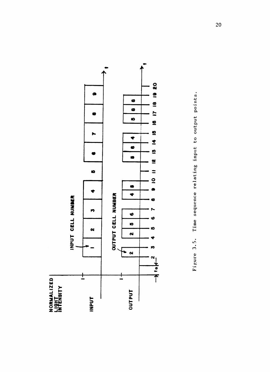
order in which they will occur. Figure 3.5 shows the mappings on a
time scale. This shows the same thing as Table 3.1, except that it
shows what is happening over the period of scan time. The light that
shines through pixel 1 will be diffracted to point 2 on the output
plane for a period of time equal to t^ seconds each.
With nine input points and a maximum of two mappings per input
pixel, it is possible to do the entire operation in eighteen time
units. This was expanded to twenty time units because decade counters
were going to be used in the digital logic. This allowed two time
units for a starting point.
Figure 3.6 shows a block diagram of the experimental layout.
Rather than scanning an actual 3 x 3 image, a shutter was opened and
closed to simulate the scanning of the image. Digital logic was de
signed to control the shutter, and the input voltage levels to the two
VCO's. A single photodetector was used at the output plane. To make
measurements, it was moved to the particular output point, and the

0
0
0
1
0
0
0
0
0
h ( i , i ;M )
0
0
0
0
0
0
0
1
0
h(i,i;l ,3)
0
0
0
0
0
0
0
0
0
h ( i j ; 2 ,2 )
0
1
0
0
0
0
0
0
0
h ( i , i ; 3J )
0
0
0
0
0
1
0
0
0
0
0
0
1
1
0
0
0
0
h(ij;l,2)
0
1
0
0
1
0
0
0
0
h(iJ;2J)
0
0
0
0
I
0
0
1
0
h(U;2,3)
0
0
0
0
1
i
0
0
0
18
h(ij;3,2)
h(i,i;3,3)
Figure 3.4. Backprojection point spread functions.

Table 3.1
Input-to-Output Mappings
19
Input Point
1 2 3 4 5 6 7 8 9
Output Point(s) I
2 ( 2 and 5 | 6 1 4 and 5 ) none | 5 and 6 | 4 i 5 and 8 |
! 8 1
20
o
a.
M
Ul
o
a.
3
•
•
m
m
•
(0
o
M
o
eo
S
o
•
S
ca
o N >
a.
N
CO
1 f
«
o a u o a 4-1 3 O
o u
a c 405 C
• H 4J CO
f—^
0) Wi
0) o c a; 3 O * 0) CO
<!} S
•H H
u-i
ro
3 6C

21
c (1) s
•H ;-i
<u a X
u o
M-l
4J 3 O >,
c <u s a
•H 3 xy
VJ3
<U
3
-r-t

22
light intensity was measured during the total scan time. The output
from the photodetector was in the form of a voltage. This voltage was
stored in a RC circuit (integrator) until it could be measured with a
voltmeter. The capacitor was then discharged and the photodetector was
moved to the next output location.
Equipment
A Lexel Model 95 Argon-ion laser was used for this experiment. The
laser power was set at 450 mW at the 514.5 nm wavelength. The laser
beam was switched on and off by a Uniblitz Model 262 Shutter [13]
powered by the Model 310B Shutter Timer Control. Two Isomet OPT-1
AOM's were used to deflect (by diffraction) the laser beam. The hori
zontal modulator was driven by a Model rf 805 Amplifier [14] which
amplified the signal from the Motorola MC1648P VCO chip. The vertical
channel was driven by two Hewlett Packard Model 460 Wide Band Ampli
fiers hooked up in series. The VCO circuit used is shown in Figure
3.7. The output light intensity was measured using a Bell and Howell
509-50 photodetector. The voltage from the photodetector was stored in
an RC circuit consisting of an adjustable 25 kQ resistor and a 50 uf
capacitor. The voltage across the capacitor was measured with a Radio
Shack Model 22-204 Multitester on the 50 VDC scale. For the photo
graphs shown in Figure 3.13 (page 34), Polaroid Type 51 film was used
with a Type 545 Land Film Holder.
Development of the Digital Logic
What was needed was a way to simultaneously deliver both a signal

23
0 - 3 0 VDC + 5 VDC
10
.l^f
i k n
12
5ftf SK3320
14
MCI648P l ^ f out
rr^
I .IM^
L- 22 turns of 20 guage wire with 1/4** inside diameter.
Figure 3.7. Diagram of VCO circuit

24
to the shutter controller and one of three different voltage levels to
the two VCO's. With nine input points and a maximum of two mappings,
eighteen units of time were needed in order to represent the processor.
After considering several possibilities, it was decided that the easi
est way to time the experiment was with decade counters. A CMOS 4011
chip was used for a clock (see Figure 3.8). Using a variable resistor
in the circuit allowed for easy changes in the clock rate. A count-to-
twenty circuit was built using two CMOS 4017 Decade Counter chips and
twenty AND gates (CMOS 4081). Using Table 3.1 and Figure 3.5, it was
possible to design the necessary logic for the shutter and the two
VCO's. Figure 3.9 shows a diagram of the digital logic employed.
Three outputs were needed. Based on Figure 3.5, the shutter
needed an "off" signal for the first, second, tenth, and eleventh time
periods. This was done by using a CMOS 4002 Quad Nor gate chip. Table
3.2 shows how the horizontal and vertical outputs were chosen using the
coordinate system in Figure 3.10. A set of CMOS 4071 and CMOS 4072 OR
gate chips were used to realize the outputs for the horizontal and
vertical controls. These outputs were tied to six 2N2222 NPN transis
tors which controlled the voltage drop across the 10 kft resistor. This
voltage became the input for the VCO's. In this way, it was possible
to get three different voltage levels to the VCO's.
In order to make the system more flexible, it was desirable to
interface a computer to drive the outputs. An Apple III microcomputer
was used because of its availability. The interface was designed by
Jones [15] and updated by Chase [16] for use with a Compucolor micro
computer. This equipment was adapted to the Apple III by Brent Boren.

25
H40U J^
lOOKa
pL&vnc
aaoKiL
CLOCK OUT
Figure 3.8. Diagram of clock circuit

26
Figure 3.9. Digital logic diagram.
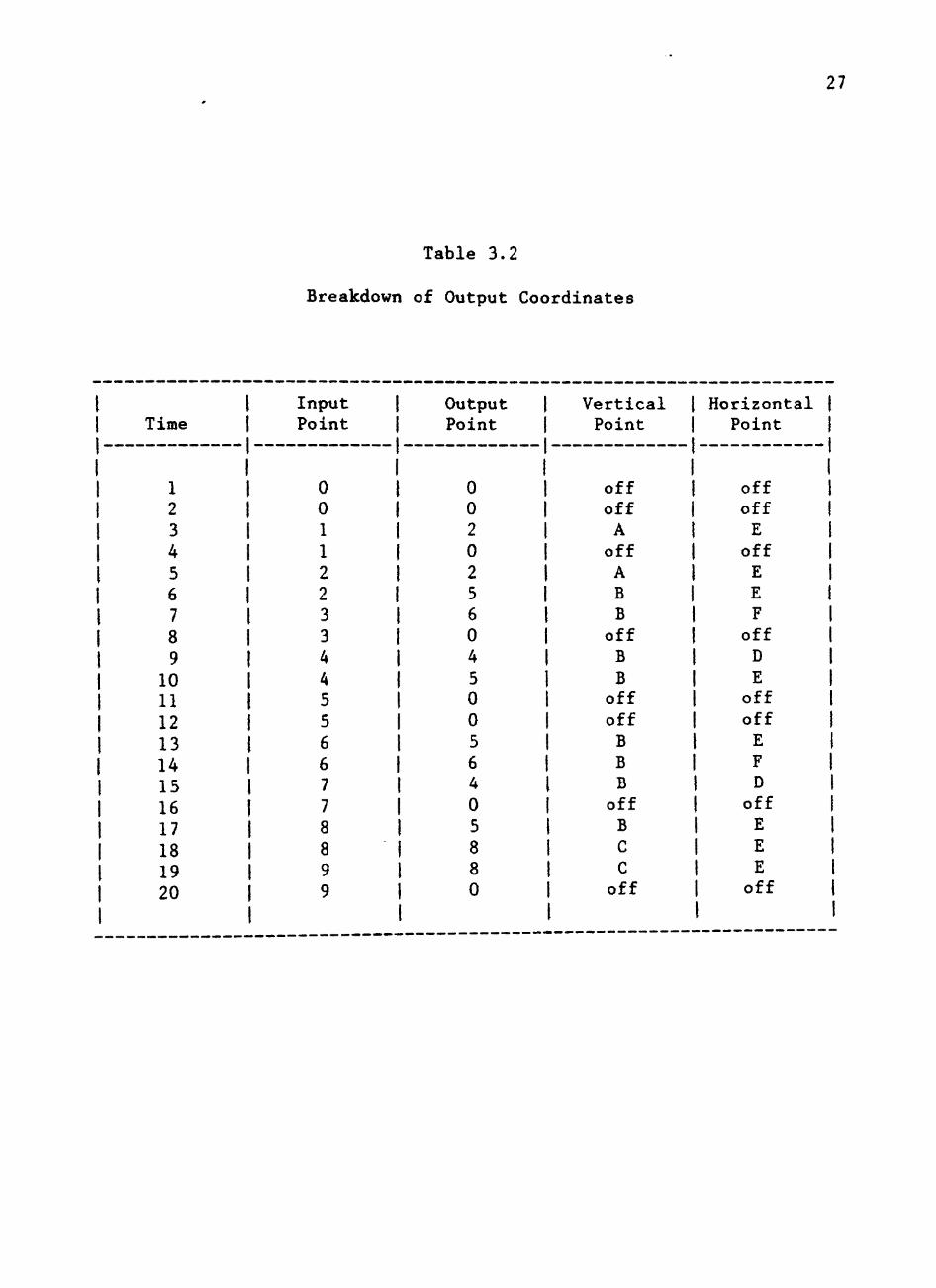
Table 3.2
Breakdown of Output Coordinates
27
j Time i
1 1 1 2 1 3 1 ^ 1 5 i 6 1 1 7
i 8 1 9 1 10 1 11 1 12 1 13 1 14 1 15 1 16 I 17 1 18 1 19 1 20
Input 1 Point
0 0 ! 1 1 2 2 1 3 3 4 4 5 5 6 6 7 7
1 8 1 8 I 9 ! 9
Output 1 Point 1
0 I 0 i 2 1 0 I 2 ! 5 ! 6 0 4 5 0 0 5 6 4 0
! 5 1 8 1 8 1 0
Vertical | Point 1
off 1 off i A ! off 1 A 1 B 1 B ! off i B B off off B B B off
1 B 1 c 1 c 1 off
Horizontal Point
off off E off E E F off D E off off E F D off
1 E 1 E 1 E 1 off

28
VERTICAL COORDINATES B
1
4
7
2
5
8
3
6
9
HORIZONTAL COORDINATES
Figure 3.10. Coordinate system for Table 3.2.

29
Figure 3.11 shows a diagram of the interface. The program was done in
BASIC and essentially instructed the 6502 microprocessor chip in the
Apple III computer to give digital output signals to the D/A converters
in the interface. This was accomplished with the POKE command. It is
possible to get one of 256 different voltage levels between zero and
10 VDC. The output time length t^ is governed by the use of FOR-TO
loops. After POKEing a particular voltage level, a time delay is
written into the program to control the length of the voltage pulse. It
was found experimentally that the fastest time pulses were 9 ms. A
sample program is given in the Appendix. The Apple II Emulation soft
ware was needed to run this program on the Apple III.
Results
Two measurements and several pictures were made with the equipment
described for the proof-of-principle experiment. These values are
shown in Figure 3.12. Figure 3.12a shows the desired results, and can
be compared with the measured results of Figures 3.12b and 3.12c. As
can be seen, the two sets of measured results are close to the desired
results. The deviations were due to measurement errors.
It was found that the VCO needed at least 300 ms in order to
switch frequencies. Attempting to switch any faster would not allow
the VCO to reach the correct output frequency. That made the total
input scan time 5.4 s. Because of the long integration time, there was
some noticeable leakage in the RC circuit. This was due to the current
leaking through the multitester which was a parallel circuit to the
capacitor.

30
BITI(MSB) , H i
I
BIT 6
OUT
- 1 =nBIT lO(LSB)
/ 10 INPUTS DIGITAL DATA
Figure 3.11. Interface diagram.

2 0
4 2
31
a) Desired results
0
2.00
0
2.08
4.00
2.29
0
1.75
0
b) 1st measurement
0
2.25
0
1.67
3.43
2.00
0
1.75
0
c) 2nd measurement
Figure 3.12. Desired results, first measurement, and second measurement.

32
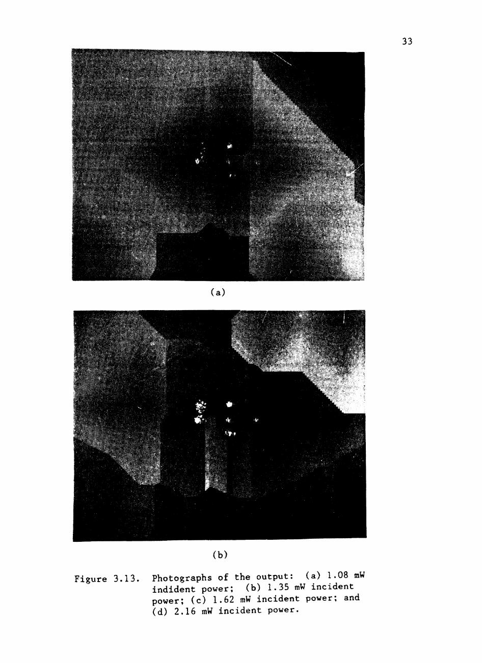
Several attempts were made to record the output on film. Figure
3.13a shows the output with 1.08 mW of incident laser light power as
measured with a NRC Model 820 laser power meter. This was measured at
the input of the crossed AOM's. Figure 3.13b was taken with 1.35 mW of
input light power. The "fragmented" appearance of the output in the
top left corner was due to reflections off of the equipment. Figures
3.13c and 3.13d were made with 1.62 mW and 2.16 mW, respectively.
Development time was thirty seconds and all pictures were taken at room
temperature. Figure 3.14 shows a picture of the equipment layout. The
next chapter will consider the capabilities and limitations of this
experiment.
33
(a)
Figure 3.13.
(b)
Photographs of the output: (a) 1.08 mW indident power; (b) 1.35 mW incident power; (c) 1.62 mW incident power; and (d) 2.16 mW incident power.

34
( c )
(d )
Figure 3.13 (Continued)

35
c S
a •H 3 U"
14-1
o Xi
a u ta o u o
^
u 3
•H

CHAPTER IV
USES AND LIMITATIONS OF DESIGN
Present System Capability
The Apple III computer using the Apple II Emulation software is
capable of running at 9 ms per cycle. This means that the fastest it
can change from one voltage level to another is 9 ms. A sample program
is given in the Appendix. With the interface described in Chapter 3,
the Apple III is able to output one of 256 voltage levels ranging from
0 to 10 V. With the crossed modulators, this gives the capability of
addressing a 256 x 256 point output array. With the current operating
capability of the Apple III, it would be able to scan all the points in
the array in 9.83 minutes. If the input image is also 256 x 256
points, it would take 447 days, 9 hrs, 25 m, 5.66 s to map all of the
input points to all of the output points. Of course, this would be the
worst case situation. If it were not necessary to map each input point
to all of the output points, then the processing would be potentially
much faster.
The typical maximum integrating time for most CCD arrays operating
at room temperature is 5 ms [17]. Thus, in its present state, the
system would not be able to use a CCD device for the output.
With the purchase of two Isomet Model DlOO-1 VCO deflector driv
ers, it would be possible to change frequencies at a rate of 1 MHz/us.
The bandwidth is 30 MHz, so the line rate for this device would be
33,333 lines/s or 30 us per line. Considering a 256 x 256 output array
36

37
again, it would take 7.68 ms for one complete scan of the output array,
and 8 m, 23 s for a complete mapping of input plane to output plane.
Again, this is clearly the worst case situation.
The ultimate capabilities of the AOM's used here have not been
tested experimentally because of limitations in the drivers. It is
possible to consider some theoretical limits to the modulators' capa
bilities. The Isomet OPT-1 AOM has a frequency range of 30 MHz to
60 MHz. Consider that it takes at least one full wave period at a
given frequency in order to achieve the required diffraction; then it
would take about 6 us to sweep one line. This was computed by dividing
the 30 MHz frequency range into 256 parts and computing the time for
one wavelength at each different frequency. It resulted in the follow
ing series:
1 1 1 1
30M 30M +2!^ ^̂ ^ ̂ ̂ ^IsS^ ^°^
which can be manipulated and reduced to the following form:
255 255 1 T . 2 (4.2)
30M n-0 255 + n
Solving Equation (4.2) analytically gives about a 6 us line sweep time.
Considering again the worst case possibility, it would take 1 m,
40.66 s to process a 256 x 256 input to ouput mapping. The next
section will compare these values to the requirements for real time
processing.

38
Limitations in the System Design
As a real time processor, a television picture is usually consid
ered as the lower limit of resolution. A television picture is made up
of 525 lines that change at a rate of 30 frames/s. This implies a line
scan time of about 63.5 us. Although each line is an analog signal,
consider it to be made up of 525 pixels and that each frame is
525 X 525 pixels. The actual number of lines used in a normal televi
sion picture is less than 525 lines because some of the lines are used
for the vertical sync signal.
If the input is 525 x 525 points, then the line time for a total
-12 mapping is about 230 x 10 s, which is considerably faster than the
approximately 12.1 us needed for a 525 point line by the AOM. In order
to keep the 30 frames/s, the modulator-driver combination would be
capable of mapping only a 14 x 14 input pixel array to a 14 x 14 output
pixel array. A 525 x 525 pixel input-to-output mapping would take
29 m, 10.9 s based on a 12.1 us line sweep time.
The Apple III has an internal clock rate of 2 MHz. Using machine
language and allowing ten steps for each voltage shift, it would have a
line sweep time of 2.63 ms. Thus, for a 525 x 525 input-to-output
mapping, it would require 4 days, 9 hrs, 30 m, and 45.7 s. A computer
would need a clock rate of 84 MHz in order to operate at television
frame rate. The Apple III would be capable of doing a 12 x 12 input-
to-output mapping at television frame rates. Also, for the VCO driver
to operate in this real-time scheme, it would require a slew rate of
about 130,000 MHz/us. In terms of achieving a real-time processor, the
equipment available is very limited. The next chapter will consider

39
all the possibilities and limitations of this design and the conclu
sions that can be drawn from this experiment. We will also consider
some possibilities for future research.

CHAPTER V
CONCLUSIONS AND FUTURE RESEARCH
Based on the results presented in Chapter 3. it has been shown
that the processor is capable of space-variant processing and is not
limited by separability of the input or the point spread function. In
terms of a real-time processor, the calculations in Chapter 4 demon
strated the limitations of the particular hardware used in this experi
ment. The calculations showed that the AOM was capable of performing
at realistic processing times (less than two minutes per picture
frame) , but improvements are needed in the VCO drivers and the com
puter.
The biggest problem was the time required to map each of the input
points to each of the output points. If the number of required input-
to-output mappings is limited, the real-time processing would be possi
ble. For example, if each input of a 525 x 525 image is mapped to only
ten output points, then there would be a total of about 2.8 x 10
mappings as compared to about 7.6 x 10 mappings in a full input-to-
output mapping. This would allow the processor to run about 27,000
times faster.
Several simplifications were made for the proof-of-principle
experiment. One of these was the use of binary inputs and point spread
functions. For future research, it would be interesting to test the
ability of the processor to handle different values of input intensi
ties and point spread functions. This can be done by temporally
40

41
changing the input rf power to the AOM. Another area of interest would
be to program the Apple III microcomputer in assembly language in order
to utilize its 2 MHz operating speed. With this capability and the new
Isomet drivers, it should be possible to use the CCD array at the
output. It would also be possible to test the physical limits of the
AOM. One question that needs to be answered is whether or not the AOM
is capable of operating at its theoretical limits. The answer to that
question awaits further research.

[1
[2
[3
LIST OF REFERENCES
J. F. Walkup, "Space-Variant Coherent Optical Processing," Optical Engineering. ]^, 339-346, 1980.
J. W. Goodman, Introduction to Fourier Optics. McGraw-Hill Book Co., San Francisco, California, 1968.
T. C. Strand and A. A. Sawchuk, "Space-Variant Processing with Polychromatic Light," Proc. of ICO-11 Conference, Madrid, Spain, 269-272, 1978 (J. Bescos, et al., Eds.).
[4] S. K. Case, "Fourier Processing in the Object Plane," Optical Letters, 4, 286-288, 1979.
[5] R. F. Carson, "Incoherent Optical Processing: A Tristiraulus-Based Approach," M.S. thesis, Dept. of Electrical Engineering. Texas Tech University, August, 1982.
[6] J. M. Adams, J. F. Walkup. T. F. Krile, and J. Shamir, "Two-Dimensional White-Light Space-Variant Processing," SPIE Proceeding, 388, 30-37, 1983.
[7] I. Glaser, "Lenslet Array Processors," Applied Optics, 21, 1271-1280, 1982. "~
[8] P. R. Haugen, H. Bartelt, and S. K. Case, "Image Formation by Multifacet Holograms," Applied Optics. 22. 1983.
[9] J. W. Goodman, "Linear Space-Variant Optical Data Processing," in Optical Information Processing Fundamentals, "Topics in Applied Physics," vol. 48, S. Heidelberg, New York, 1981.
[10] T. Kailath, "Channel Characterization: Time-Variant Dispersive Channels," in Lectures on Communication System Theory, Chapter 6, (E. J. Baghdady, Ed.).
[11] N. J. Berg and J. N. Lee (Eds.). Acousto-Optic Signal Processing. Marcel Dekker. Inc.. New York, 1983.
[12] J. Sapriel, Acousto-Optics, John Wiley and Sons, New York, 1979.
[13] A. W. Vincent Associates, Inc., Rochester, New York 14607.
[14] R. F. Communications, Rochester, New York 14610.
[15] B. H. Jones III, "A Laser Plotter for Optical Processing," M.S. thesis, Dept. of Electrical Engineering, Texas Tech University, January, 1982.
42

43
[16] S. Chase. "Fabrication of Binary Phase Diffusers for Space-Variant Processing," M.S. thesis, Dept. of Electrical Engineering, Texas Tech University, December, 1983.
[17] Fairchild, CCD: The Solid State Imaging Technology, Palo Alto, California 94304.

APPENDIX
COMPUTER PROGRAM
This program will drive a shutter and both VCO's in order to
produce the same results as the digital logic used for the experiment
10 REM VCO DRIVER PROGRAM
15 X-49647:Y-49661:S-49655
17 REM SET STARTING VALUES
20 POKE X,0:P0KE Y,0:P0KE S,0
22 REM DELAY LOOP
25 FOR I-l TO 170:NEXT I
27 REM SECOND TIME UNIT
30 POKE X,0:POKE Y,0:P0KE S.O
35 FOR I-l TO 170:NEXT I
37 REM THIRD TIME UNIT
40 POKE X,200:P0KE Y,255:POKE S,255
45 FOR I-l TO 170:NEXT I
47 REM FOURTH TIME UNIT
50 POKE X,0:P0KE Y,0
55 FOR I-l TO 170:NEXT I
60 POKE X,200:POKE Y,255
65 FOR I-l TO 170:NEXT I
70 POKE X,200:POKE Y.200
75 FOR I-l TO 170:NEXT I
44

45
80 POKE X.255:P0KE Y,200
90 FOR I-l TO 170:NEXT I
95 POKE X,0:P0KE Y.O
100 FOR I-l TO 170:NEXT I
105 POKE X,155:P0KE Y.200
110 FOR I-l TO 170:NEXT I
115 POKE X,200:POKE Y,200
120 FOR I-l TO 170:NEXT I
125 POKE X,0:POKE Y,0:POKE S,0
130 FOR I-l TO 170:NEXT I
135 POKE X,0:P0KE Y.O:POKE S.O
140 FOR I-l TO 170:NEXT I
145 POKE X,200:POKE Y.200:POKE S,255
150 FOR I-l TO 170:NEXT I
155 POKE X,255:POKE Y,200
160 FOR I-l TO 170:NEXT I
165 POKE X,155:POKE Y,200
170 FOR I-l TO 170:NEXT I
175 POKE X,0:POKE Y.O
180 FOR I-l TO 170:NEXT I
185 POKE X,200:P0KE Y,200
190 FOR I-l TO 170:NEXT I
195 POKE X,200:POKE Y,155
200 FOR I-l TO 170:NEXT I
205 POKE X.200:POKE Y,155
210 FOR I-l TO 170:NEXT I

46
215 POKE X,0:POKE Y.O
220 FOR I-l TO 170-.NEXT I
225 GO TO 20