SP339E DS - atta.szlcsc.com
24
1 SP339E RS-232/RS-485/RS-422 TRANSCEIVER WITH INTERNAL TERMINATION JANUARY 2019 REV. 1.0.6 GENERAL DESCRIPTION The SP339 is an advanced multiprotocol transceiver supporting RS-232, RS-485, and RS-422 serial standards in a 40 pin QFN package. Integrated cable termination and four configuration modes allow all three protocols to be used interchangeably over a single cable or connector with no additional switching components. Full operation requires only four external charge pump capacitors. The RS-485/422 modes feature one driver and one receiver (1TX/1RX) in both half and full duplex configurations. The RS-232 mode (3TX/5RX) provides full support of all eight signals commonly used with the DB9 RS-232 connector. A dedicated diagnostic loopback mode is also provided. The high speed drivers operate up to 20Mbps in RS- 485/422 modes, and up to 1Mbps in RS-232 mode. All drivers can be slew limited to 250kbps in any mode to minimize electromagnetic interference (EMI). All transmitter outputs and receiver inputs feature robust electrostatic discharge (ESD) protection to ±15kV IEC-61000-4-2 Air Gap, ±8kV IEC-61000-4-2 Contact, and ±15kV Human Body Model (HBM). Each receiver output has full fail-safe protection to avoid system lockup, oscillation, or indeterminate states by defaulting to logic-high output level when the inputs are open, shorted, or terminated but undriven. No external biasing resistors are required. The RS-232 receiver inputs include a 5k pull-down to ground. The RS-485/422 receiver inputs are high impedance (>96k when termination is disabled), allowing up to 256 devices on a single communication bus (1/8th unit load). The SP339 operates from a single power supply, either 3.3V or 5V, with low idle current (2mA typical in all modes). The shutdown mode consumes less than 10µA for low power standby operation. FEATURES Pin selectable Cable Termination No external resistors required for RS-485/422 termination and biasing 3.3V or 5V Single Supply Operation Robust ESD Protection on bus pins n ±15kV IEC 61000-4-2 (Air Gap) n ± 8kV IEC 61000-4-2 (Contact) n ±15kV Human Body Model (HBM) Max Data Rate of 20Mbps in RS-485/422 Modes and up to 1Mbps in RS-232 Modes Pin selectable 250kbps Slew Limiting 3 Drivers, 5 Receivers RS-232/V.28 1 Driver, 1 Receiver RS-485/422 n Full and Half Duplex Configuration n 1/8th Unit Load, up to 256 receivers on bus RS-485/422 Enhanced Failsafe for open, shorted, or terminated but idle inputs Space saving 6mm x 6mm QFN-40 Package Pin compatible with SP338E TYPICAL APPLICATIONS Dual Protocol Serial Ports (RS-232 or RS-485/422) Industrial Computers Industrial and Process Control Equipment Point-Of-Sale Equipment Networking Equipment HVAC Controls Equipment Building Security and Automation Equipment ORDERING INFORMATION (1) P ART NUMBER OPERATING TEMPERATURE RANGE LEAD-FREE P ACKAGE P ACKAGING METHOD SP339EER1-L -40°C to +85°C Yes (2) 40-pin QFN Tray SP339EER1-L/TR -40°C to +85°C 40-pin QFN Tape and Reel NOTE: 1. Refer to www.exar.com/SP339E for most up-to-date Ordering Information. 2. Visit www.exar.com for additional information on Environmental Rating.
Transcript of SP339E DS - atta.szlcsc.com

1
SP339ERS-232/RS-485/RS-422 TRANSCEIVER WITH INTERNAL TERMINATION
JANUARY 2019 REV. 1.0.6
GENERAL DESCRIPTIONThe SP339 is an advanced multiprotocol transceiversupporting RS-232, RS-485, and RS-422 serialstandards in a 40 pin QFN package. Integrated cabletermination and four configuration modes allow allthree protocols to be used interchangeably over asingle cable or connector with no additional switchingcomponents. Full operation requires only fourexternal charge pump capacitors.
The RS-485/422 modes feature one driver and onereceiver (1TX/1RX) in both half and full duplexconfigurations. The RS-232 mode (3TX/5RX)provides full support of all eight signals commonlyused with the DB9 RS-232 connector. A dedicateddiagnostic loopback mode is also provided.
The high speed drivers operate up to 20Mbps in RS-485/422 modes, and up to 1Mbps in RS-232 mode.All drivers can be slew limited to 250kbps in anymode to minimize electromagnetic interference (EMI).
All transmitter outputs and receiver inputs featurerobust electrostatic discharge (ESD) protection to±15kV IEC-61000-4-2 Air Gap, ±8kV IEC-61000-4-2Contact, and ±15kV Human Body Model (HBM).Each receiver output has full fail-safe protection toavoid system lockup, oscillation, or indeterminatestates by defaulting to logic-high output level whenthe inputs are open, shorted, or terminated butundriven. No external biasing resistors are required.
The RS-232 receiver inputs include a 5k pull-downto ground. The RS-485/422 receiver inputs are highimpedance (>96k when termination is disabled),allowing up to 256 devices on a singlecommunication bus (1/8th unit load).
The SP339 operates from a single power supply,either 3.3V or 5V, with low idle current (2mA typical inall modes). The shutdown mode consumes less than10µA for low power standby operation.
FEATURES
Pin selectable Cable Termination
No external resistors required for RS-485/422termination and biasing
3.3V or 5V Single Supply Operation
Robust ESD Protection on bus pinsn ±15kV IEC 61000-4-2 (Air Gap)n ± 8kV IEC 61000-4-2 (Contact)n ±15kV Human Body Model (HBM)
Max Data Rate of 20Mbps in RS-485/422 Modesand up to 1Mbps in RS-232 Modes
Pin selectable 250kbps Slew Limiting
3 Drivers, 5 Receivers RS-232/V.28
1 Driver, 1 Receiver RS-485/422n Full and Half Duplex Configurationn 1/8th Unit Load, up to 256 receivers on bus
RS-485/422 Enhanced Failsafe for open, shorted,or terminated but idle inputs
Space saving 6mm x 6mm QFN-40 Package
Pin compatible with SP338E
TYPICAL APPLICATIONS
Dual Protocol Serial Ports (RS-232 or RS-485/422)
Industrial Computers
Industrial and Process Control Equipment
Point-Of-Sale Equipment
Networking Equipment
HVAC Controls Equipment
Building Security and Automation Equipment
ORDERING INFORMATION(1)
PART NUMBER OPERATING TEMPERATURE RANGE LEAD-FREE PACKAGE PACKAGING METHOD
SP339EER1-L -40°C to +85°CYes(2)
40-pin QFN Tray
SP339EER1-L/TR -40°C to +85°C 40-pin QFN Tape and Reel
NOTE:1. Refer to www.exar.com/SP339E for most up-to-date Ordering Information.2. Visit www.exar.com for additional information on Environmental Rating.
SP339E
2
RS-232/RS-485/RS-422 TRANSCEIVER WITH INTERNAL TERMINATION REV. 1.0.6
CAUTION: ESD (ElectroStatic Discharge) sensitive device. Permanent damage may occur on unconnected devices subject to highenergy electrostatic fields. Unused devices must be stored in conductive foam or shunts. Personnel should be properlygrounded prior to handling this device. The protective foam should be discharged to the destination socket before devicesare removed.
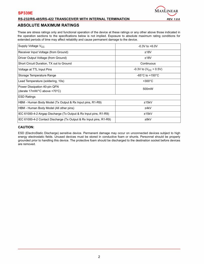
ABSOLUTE MAXIMUM RATINGSThese are stress ratings only and functional operation of the device at these ratings or any other above those indicated inthe operation sections to the specifications below is not implied. Exposure to absolute maximum rating conditions forextended periods of time may affect reliability and cause permanent damage to the device.
Supply Voltage VCC -0.3V to +6.0V
Receiver Input Voltage (from Ground) ±18V
Driver Output Voltage (from Ground) ±18V
Short Circuit Duration, TX out to Ground Continuous
Voltage at TTL Input Pins -0.3V to (VCC + 0.5V)
Storage Temperature Range -65°C to +150°C
Lead Temperature (soldering, 10s) +300°C
Power Dissipation 40-pin QFN(derate 17mW/°C above +70°C)
500mW
ESD Ratings
HBM - Human Body Model (Tx Output & Rx Input pins, R1-R9) ±15kV
HBM - Human Body Model (All other pins) ±4kV
IEC 61000-4-2 Airgap Discharge (Tx Output & Rx Input pins, R1-R9) ±15kV
IEC 61000-4-2 Contact Discharge (Tx Output & Rx Input pins, R1-R9) ±8kV

SP339E
3
REV. 1.0.6 RS-232/RS-485/RS-422 TRANSCEIVER WITH INTERNAL TERMINATION
PIN DESCRIPTIONS BY MODE (MODE1, MODE0)
Pin Name 00, Figure 1 01, Figure 2 10, Figure 3 11, Figure 4
1 L1 R1 Output 1 1
2 L2 R2 Output R1 Output R1 Output
3 L3 T1 Input T1 Input T1 Input
4 L4 T2 Input
5 L6 R3 Output 1 1
6 L7 T3 Input
7 L8 R4 Output 1 1
8 L9 R5 Output 1 1
9 VCC VCC
10 GND Ground
11 SLEW SLEW = VCC enables 250kbps slew limiting
12 DIR1T1 Enable,R1 Disable
T1 Enable
13 N/C This pin is not used and is not connected internally
14 MODE0 0 1 0 1
15 MODE1 0 0 1 1
16 N/C This pin is not used and is not connected internally
17 TERM Enables RS-485/422 receiver termination
18 N/C This pin is not used and is not connected internally
19 ENABLE ENABLE = VCC for operation, ENABLE = 0V for shutdown
20 VCC VCC

SP339E
4
RS-232/RS-485/RS-422 TRANSCEIVER WITH INTERNAL TERMINATION REV. 1.0.6
PIN DESCRIPTIONS BY MODE (MODE1, MODE0)
Pin Name 00, Figure 1 01, Figure 2 10, Figure 3 11, Figure 4
21 R9 R5 Input
22 R8 R4 Input
23 GND Ground
24 R7 T3 Output
25 R6 R3 Input
26 GND Ground
27 R4 T2 Output R1 Input B
28 R3 T1 Output R1 Input A
29 GND Ground
30 R2 R2 Input R1 Input A, T1 Out A T1 Out A
31 R1 R1 Input R1 Input B, T1 Out B T1 Out B
32 VCC VCC - 1.0F to ground recommended for supply decoupling
33 VSS VSS - Charge pump negative supply, 0.1F from ground
34 C2- C2+ - Charge pump cap 2 negative lead
35 C1- C1- - Charge pump cap 1 negative lead
36 GND Ground
37 C1+ C1+ - Charge pump cap 1 positive lead, 0.1F
38 VCC VCC
39 C2+ C2+ - Charge pump cap 2 positive lead, 0.1F
40 VDD VDD - Charge pump positive supply, 0.1F to ground

SP339E
5
REV. 1.0.6 RS-232/RS-485/RS-422 TRANSCEIVER WITH INTERNAL TERMINATION
SUGGESTED DB9 CONNECTOR PINOUT
DB9Pin
RS-232RS-485/422Full Duplex
RS-485Half Duplex
1 DCD TX- Data-
2 RXD TX+ Data+
3 TXD RX+
4 DTR RX-
5 Ground
6 DSR
7 RTS
8 CTS
9 RI
SP339E
6
RS-232/RS-485/RS-422 TRANSCEIVER WITH INTERNAL TERMINATION REV. 1.0.6
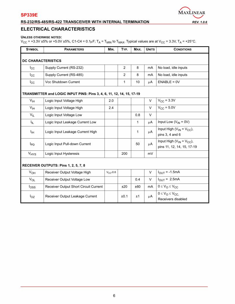
ELECTRICAL CHARACTERISTICSUNLESS OTHERWISE NOTED: VCC = +3.3V ±5% or +5.0V ±5%, C1-C4 = 0.1F; TA = TMIN to TMAX. Typical values are at VCC = 3.3V, TA = +25°C.
SYMBOL PARAMETERS MIN. TYP. MAX. UNITS CONDITIONS
DC CHARACTERISTICS
ICC Supply Current (RS-232) 2 8 mA No load, idle inputs
ICC Supply Current (RS-485) 2 8 mA No load, idle inputs
ICC Vcc Shutdown Current 1 10 A ENABLE = 0V
TRANSMITTER and LOGIC INPUT PINS: Pins 3, 4, 6, 11, 12, 14, 15, 17-19
VIH Logic Input Voltage High 2.0 V VCC = 3.3V
VIH Logic Input Voltage High 2.4 V VCC = 5.0V
VIL Logic Input Voltage Low 0.8 V
IIL Logic Input Leakage Current Low 1 A Input Low (VIN = 0V)
IIH Logic Input Leakage Current High 1 AInput High (VIN = VCC), pins 3, 4 and 6
IPD Logic Input Pull-down Current 50 AInput High (VIN = VCC), pins 11, 12, 14, 15, 17-19
VHYS Logic Input Hysteresis 200 mV
RECEIVER OUTPUTS: Pins 1, 2, 5, 7, 8
VOH Receiver Output Voltage High VCC-0.6 V IOUT = -1.5mA
VOL Receiver Output Voltage Low 0.4 V IOUT = 2.5mA
IOSS Receiver Output Short Circuit Current ±20 ±60 mA 0 VO VCC
IOZ Receiver Output Leakage Current ±0.1 ±1 A0 VO VCC,
Receivers disabled

SP339E
7
REV. 1.0.6 RS-232/RS-485/RS-422 TRANSCEIVER WITH INTERNAL TERMINATION
ELECTRICAL CHARACTERISTICS (Continued)UNLESS OTHERWISE NOTED: VCC = +3.3V ±5% or +5.0V ±5%, C1-C4 = 0.1F; TA = TMIN to TMAX. Typical values are at VCC = 3.3V, TA = +25°C.
SYMBOL PARAMETERS MIN. TYP. MAX. UNITS CONDITIONS
SINGLE-ENDED RECEIVER INPUTS (RS-232)
VIN Input Voltage Range -15 +15 V
VIL Input Threshold Low0.6 1.2 V VCC = 3.3V
0.8 1.5 V VCC = 5.0V
VIH Input Threshold High1.5 2.0 V VCC = 3.3V
1.8 2.4 V VCC = 5.0V
VHYS Input Hysteresis 0.3 V
RIN Input Resistance 3 5 7 k -15V VIN +15V
SINGLE-ENDED DRIVER OUTPUTS (RS-232)
VO Output Voltage Swing±5.0 ±5.5 V Output loaded with 3kto Gnd
±7.0 V No load output
ISC Short Circuit Current ±60 mA VO = 0V
ROFF Power Off Impedance 300 10M VCC = 0V, VO = ±2V

SP339E
8
RS-232/RS-485/RS-422 TRANSCEIVER WITH INTERNAL TERMINATION REV. 1.0.6
ELECTRICAL CHARACTERISTICS (Continued)UNLESS OTHERWISE NOTED: VCC = +3.3V ±5% or +5.0V ±5%, C1-C4 = 0.1F; TA = TMIN to TMAX. Typical values are at VCC = 3.3V, TA = +25°C.
SYMBOL PARAMETERS MIN. TYP. MAX. UNITS CONDITIONS
DIFFERENTIAL RECEIVER INPUTS (RS-485 / RS-422)
RIN Receiver Input Resistance 96 kTERM = 0V,-7V VIN +12V
VTHReceiver DifferentialThreshold Voltage
-200 -125 -50 mV
VTH Receiver Input Hysteresis 25 mV VCM = 0V
IIN Receiver Input Current125 A VIN = +12V
-100 A VIN = -7V
RTERM Termination Resistance 100 120 155 TERM = VCC, Figure 5-7V VCM +12V
RTERM Termination Resistance 100 120 140 TERM = VCC, Figure 5VCM = 0V
DIFFERENTIAL DRIVER OUTPUTS (RS-485 / RS-422)
VOD Differential Driver Output
2 VCC V RL = 100 (RS-422), Figure 6
1.5 VCC V RL = 54 (RS-485), Figure 6
1.5 VCC V -7V VCM +12V, Figure 7
VCC V No Load
VODChange In Magnitude ofDifferential Output Voltage
-0.2 +0.2 V RL = 54 or 100, Figure 6
VCM Driver Common Mode Output Voltage 3 V RL = 54 or 100, Figure 6
VCMChange In Magnitude ofCommon Mode Output Voltage
0.2 V RL = 54 or 100, Figure 6
IOSD Driver Output Short Circuit Current -250 250 mA -7V VO +12V, Figure 8
IO Driver Output Leakage Current
100 ADIR1 = 0V in Mode 11,or ENABLE = 0V,VO +12V, VCC = 0V or 5.25V
-100 ADIR1 = 0V in Mode 11,or ENABLE = 0V,VO -7V, VCC = 0V or 5.25V
SP339E
9
REV. 1.0.6 RS-232/RS-485/RS-422 TRANSCEIVER WITH INTERNAL TERMINATION
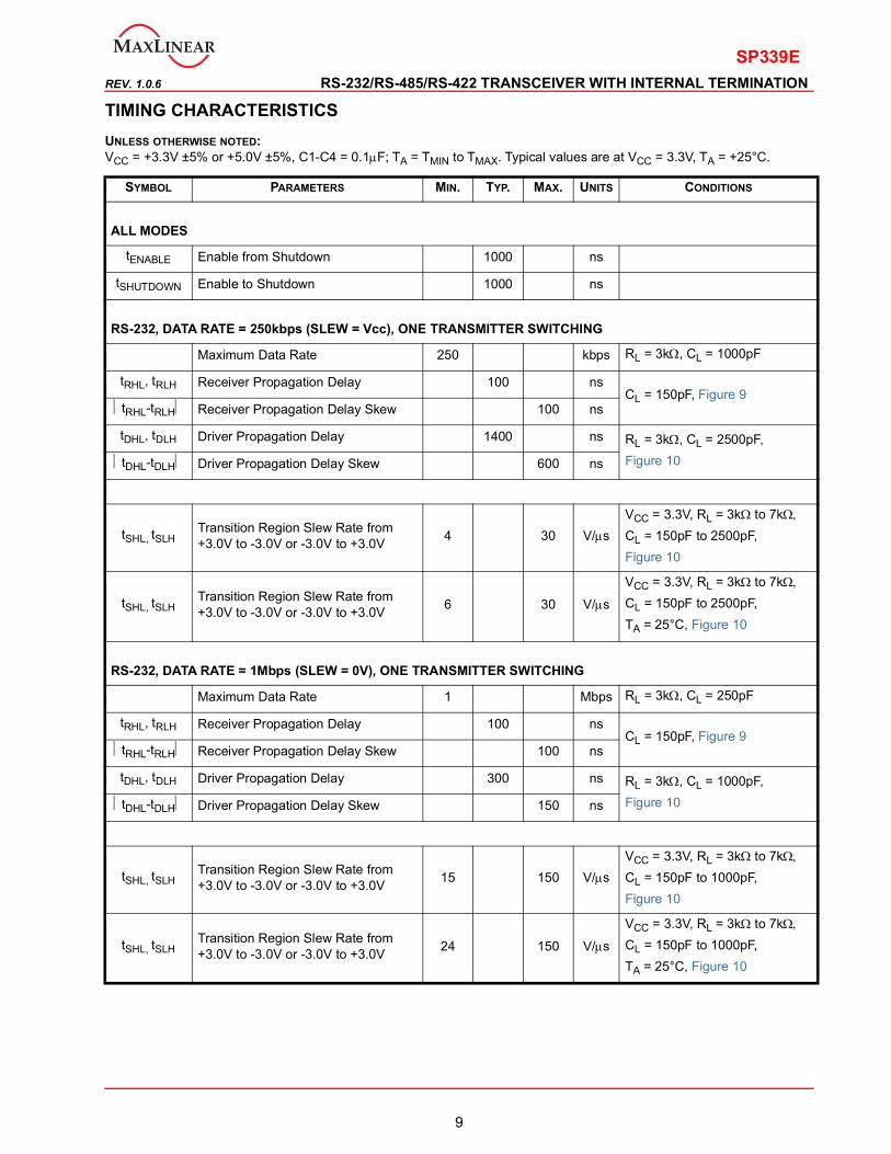
TIMING CHARACTERISTICSUNLESS OTHERWISE NOTED: VCC = +3.3V ±5% or +5.0V ±5%, C1-C4 = 0.1F; TA = TMIN to TMAX. Typical values are at VCC = 3.3V, TA = +25°C.
SYMBOL PARAMETERS MIN. TYP. MAX. UNITS CONDITIONS
ALL MODES
tENABLE Enable from Shutdown 1000 ns
tSHUTDOWN Enable to Shutdown 1000 ns
RS-232, DATA RATE = 250kbps (SLEW = Vcc), ONE TRANSMITTER SWITCHING
Maximum Data Rate 250 kbps RL = 3k, CL = 1000pF
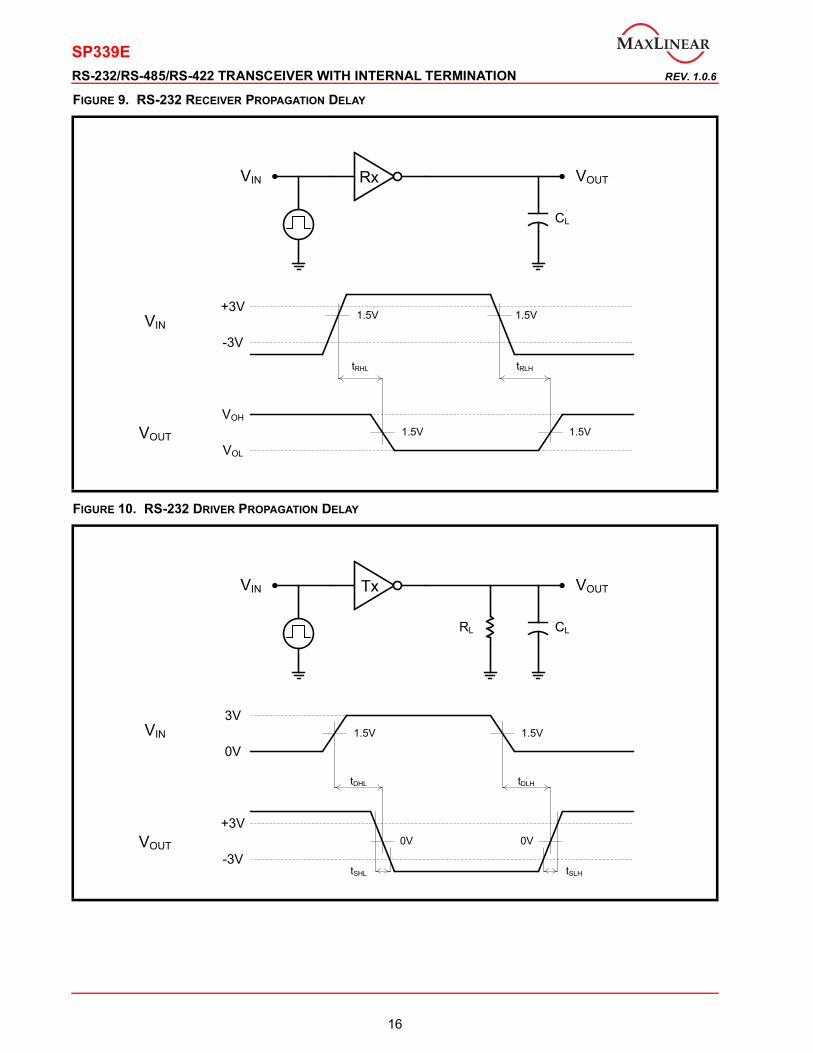
tRHL, tRLH Receiver Propagation Delay 100 nsCL = 150pF, Figure 9
tRHL-tRLH Receiver Propagation Delay Skew 100 ns
tDHL, tDLH Driver Propagation Delay 1400 ns RL = 3k, CL = 2500pF,Figure 10tDHL-tDLH Driver Propagation Delay Skew 600 ns
tSHL, tSLHTransition Region Slew Rate from +3.0V to -3.0V or -3.0V to +3.0V 4 30 V/s
VCC = 3.3V, RL = 3k to 7kCL = 150pF to 2500pF,Figure 10
tSHL, tSLHTransition Region Slew Rate from +3.0V to -3.0V or -3.0V to +3.0V 6 30 V/s
VCC = 3.3V, RL = 3k to 7kCL = 150pF to 2500pF,TA = 25°C, Figure 10
RS-232, DATA RATE = 1Mbps (SLEW = 0V), ONE TRANSMITTER SWITCHING
Maximum Data Rate 1 Mbps RL = 3k, CL = 250pF
tRHL, tRLH Receiver Propagation Delay 100 nsCL = 150pF, Figure 9
tRHL-tRLH Receiver Propagation Delay Skew 100 ns
tDHL, tDLH Driver Propagation Delay 300 ns RL = 3k, CL = 1000pF,Figure 10tDHL-tDLH Driver Propagation Delay Skew 150 ns
tSHL, tSLHTransition Region Slew Rate from +3.0V to -3.0V or -3.0V to +3.0V 15 150 V/s
VCC = 3.3V, RL = 3k to 7kCL = 150pF to 1000pF,Figure 10
tSHL, tSLHTransition Region Slew Rate from +3.0V to -3.0V or -3.0V to +3.0V 24 150 V/s
VCC = 3.3V, RL = 3k to 7kCL = 150pF to 1000pF,TA = 25°C, Figure 10

SP339E
10
RS-232/RS-485/RS-422 TRANSCEIVER WITH INTERNAL TERMINATION REV. 1.0.6
TIMING CHARACTERISTICS (Continued)UNLESS OTHERWISE NOTED: VCC = +3.3V ±5% or +5.0V ±5%, C1-C4 = 0.1F; TA = TMIN to TMAX. Typical values are at VCC = 3.3V, TA = +25°C.
SYMBOL PARAMETERS MIN. TYP. MAX. UNITS CONDITIONS
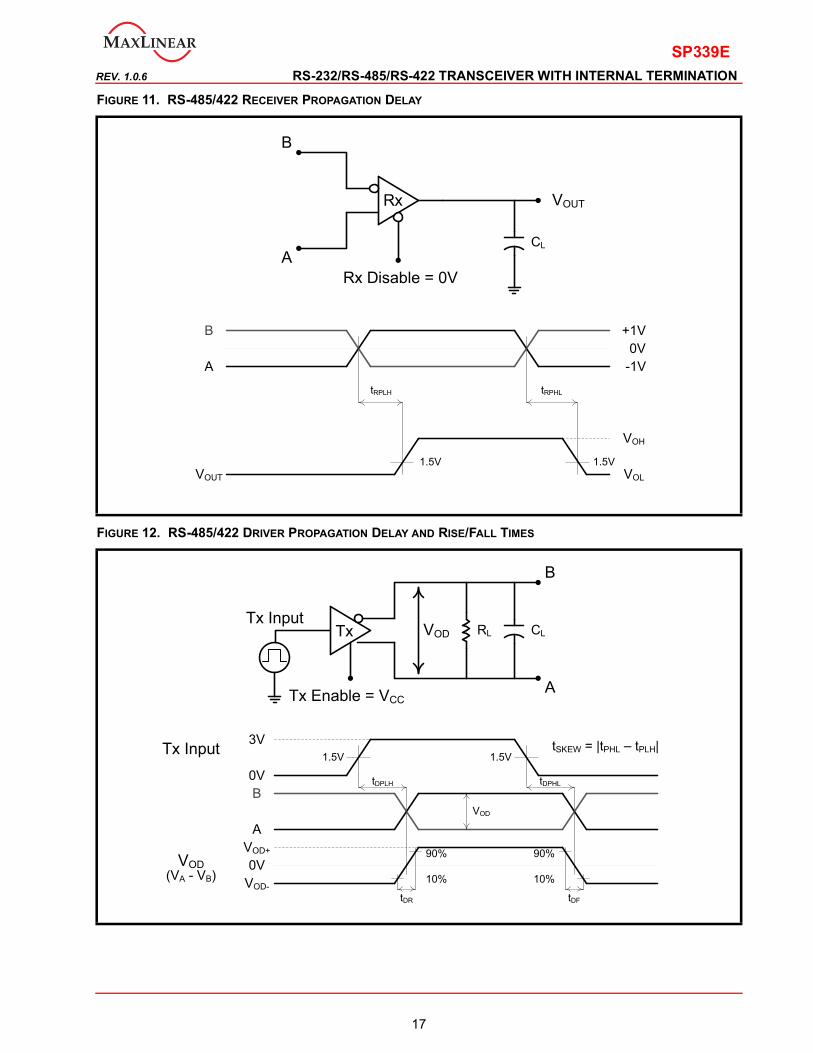
RS-485/RS-422, DATA RATE = 250kbps (SLEW = Vcc), ONE TRANSMITTER SWITCHING
Maximum Data Rate 250 kbps RL = 54CL = 50pF
tRPHL, tRPLH Receiver Propagation Delay 50 150 nsCL = 15pF, Figure 11
tRPHL-tRPLH Receiver Propagation Delay Skew 20 ns
tDPHL, tDPLH Driver Propagation Delay 500 1000 nsRL = 54CL = 50pF,Figure 12
tDPHL-tDPLH Driver Propagation Delay Skew 100 ns
tDR, tDF Driver Rise and Fall Time 300 650 1200 ns
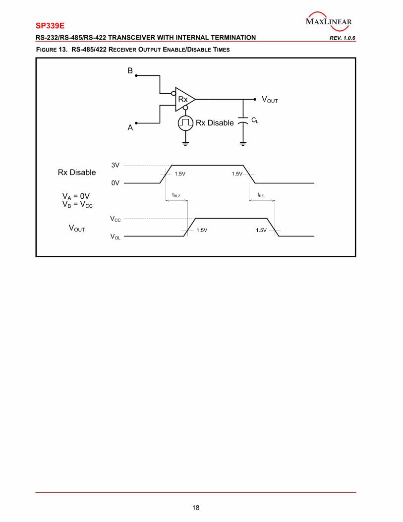
tRZH, tRZL Receiver Output Enable Time 200 nsCL = 15pF, Figure 13
tRHZ, tRLZ Receiver Output Disable Time 200 ns
tDZH, tDZL Driver Output Enable Time 1000 ns RL = 500CL = 50pF,Figure 14tDHZ, tDLZ Driver Output Disable Time 200 ns
RS-485/RS-422, DATA RATE = 20Mbps (SLEW = 0V), ONE TRANSMITTER SWITCHING
Maximum Data Rate 20 Mbps RL = 54CL = 50pF
tRPHL, tRPLH Receiver Propagation Delay 50 150 nsCL = 15pF, Figure 11
tRPHL-tRPLH Receiver Propagation Delay Skew 10 ns
tDPHL, tDPLH Driver Propagation Delay 30 100 nsRL = 54CL = 50pF,Figure 12
tDPHL-tDPLH Driver Propagation Delay Skew 10 ns
tDR, tDF Driver Rise and Fall Time 10 20 ns
tRZH, tRZL Receiver Output Enable Time 200 nsCL = 15pF, Figure 13
tRHZ, tRLZ Receiver Output Disable Time 200 ns
tDZH, tDZL Driver Output Enable Time 200 ns RL = 500CL = 50pF,Figure 14tDHZ, tDLZ Driver Output Disable Time 200 ns

SP339E
11
REV. 1.0.6 RS-232/RS-485/RS-422 TRANSCEIVER WITH INTERNAL TERMINATION
BLOCK DIAGRAM BY MODE (MODE1, MODE0)FIGURE 1. MODE 00 - LOOPBACK
Mode0=0
Mode1=0
Enable=1
Vcc
L1
L2
L3
L4
L6
L7
L8
L9
Vcc
11 12 13 14 15 16 17 18 19 20
40 39 38 37 36 35 34 33 32 31
1
2
3
4
5
6
7
8
9
10
30
29
28
27
26
25
24
23
22
21
All pull-downs 330kΩ
V+ C2+ Vcc
C1+ C1-
C2- V- Vcc
C30.1µF
C2
0.1µF C1
0.1µF C40.1µF
Cc1.0µF
R3
R4
T3
R5
T2
T1
R2
R1
SP339E
12
RS-232/RS-485/RS-422 TRANSCEIVER WITH INTERNAL TERMINATION REV. 1.0.6
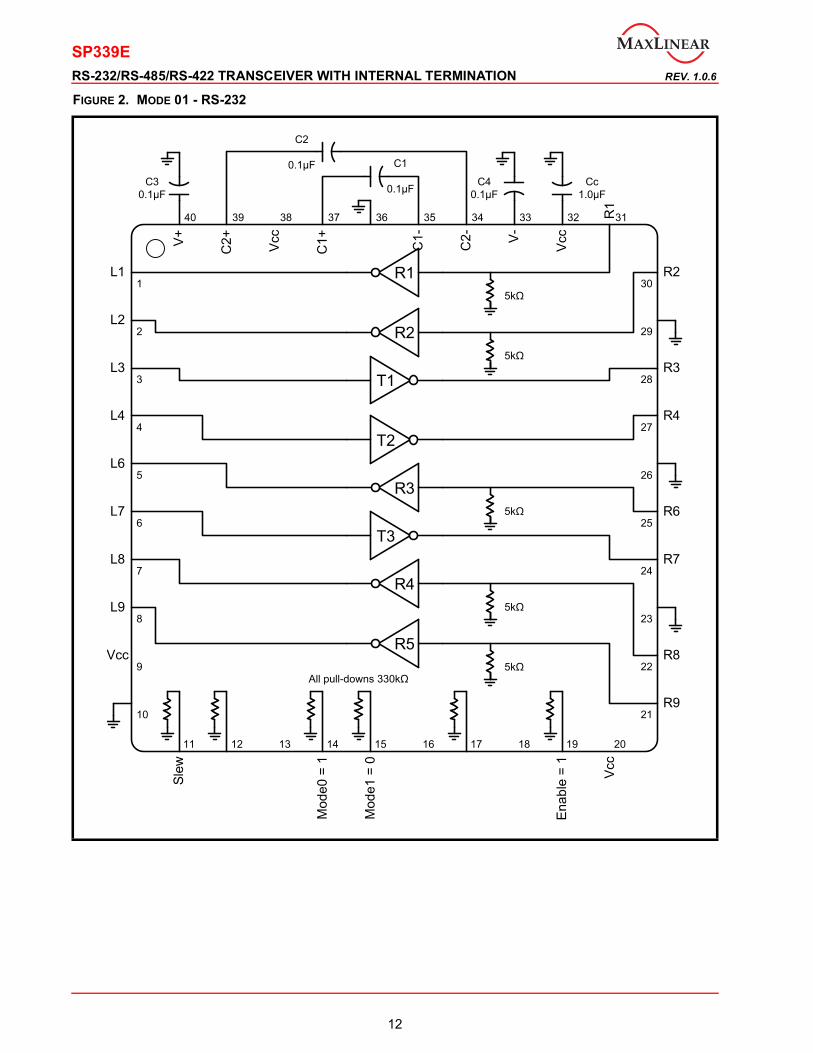
FIGURE 2. MODE 01 - RS-232
Slew
Mode0=1
Mode1=0
Enable=1
Vcc
L1
L2
L3
L4
L6
L7
L8
L9
Vcc
R2
R3
R4
R6
R7
R8
R9
11 12 13 14 15 16 17 18 19 20
40 39 38 37 36 35 34 33 32 31
1
2
3
4
5
6
7
8
9
10
30
29
28
27
26
25
24
23
22
21
All pull-downs 330kΩ
R1
V+ C2+ Vcc
C1+ C1-
C2- V- Vcc
C30.1µF
C2
0.1µF C1
0.1µF C40.1µF
Cc1.0µF
R3
R4
T3
R5
T2
T1
R2
R15kΩ
5kΩ
5kΩ
5kΩ
5kΩ

SP339E
13
REV. 1.0.6 RS-232/RS-485/RS-422 TRANSCEIVER WITH INTERNAL TERMINATION
FIGURE 3. MODE 10 - RS-485 HALF DUPLEX
Slew Dir1
Mode0=0
Mode1=1
Term
Enable=1
Vcc
L1 = 1
L2
L3
L6 = 1
L8 = 1
L9 = 1
Vcc
R1
T1R2
120Ω
11 12 13 14 15 16 17 18 19 20
40 39 38 37 36 35 34 33 32 31
1
2
3
4
5
6
7
8
9
10
30
29
28
27
26
25
24
23
22
21
All pull-downs 330kΩ
R1
V+ C2+ Vcc
C1+ C1-
C2- V- Vcc
C30.1µF
C2
0.1µF C1
0.1µF C40.1µF
Cc1.0µF

SP339E
14
RS-232/RS-485/RS-422 TRANSCEIVER WITH INTERNAL TERMINATION REV. 1.0.6
FIGURE 4. MODE 11 - RS-485/422 FULL DUPLEX
Slew Dir1
Mode0=1
Mode1=1
Term
Enable=1
Vcc
T1
R1
R2
R3
R4
11 12 13 14 15 16 17 18 19 20
40 39 38 37 36 35 34 33 32 31
1
2
3
4
5
6
7
8
9
10
30
29
28
27
26
25
24
23
22
21
120Ω
All pull-downs 330kΩ
R1
V+ C2+ Vcc
C1+ C1-
C2- V- Vcc
C30.1µF
C2
0.1µF C1
0.1µF C40.1µF
Cc1.0µF
L1 = 1
L2
L3
L6 = 1
L8 = 1
L9 = 1
Vcc

SP339E
15
REV. 1.0.6 RS-232/RS-485/RS-422 TRANSCEIVER WITH INTERNAL TERMINATION
TEST CIRCUITSFIGURE 5. RS-485/422 RECEIVER TERMINATION RESISTANCE
Termination is enabled in RS-485/422 modes when the TERM pin is held high (VCC).
FIGURE 6. RS-485/422 DIFFERENTIAL DRIVER OUTPUT VOLTAGE
FIGURE 7. RS-485/422 DIFFERENTIAL DRIVER OUTPUT VOLTAGE OVER COMMON MODE
FIGURE 8. RS-485/422 DRIVER OUTPUT SHORT CIRCUIT CURRENT
TERM = VCCIB
±2V Rx
IA
B
A
RTERM
RTERM = 2 (VA – VB)IA – IB
-7V ≤ VA, VB ≤ +12V
Tx VOD VCM
Tx Enable = VCC
Tx Input = 0V or VCC
B
A
RL2
RL2
Tx VOD VCM60Ω
375Ω
375Ω
B
ATx Enable = VCC
Tx Input = 0V or VCC
Tx
-7V to +12V V
B
A
IOSD
Tx Enable = 0V or VCC
Tx Input = 0V or VCC
SP339E
16
RS-232/RS-485/RS-422 TRANSCEIVER WITH INTERNAL TERMINATION REV. 1.0.6
FIGURE 9. RS-232 RECEIVER PROPAGATION DELAY
FIGURE 10. RS-232 DRIVER PROPAGATION DELAY
CL
RxVIN VOUT
+3V
-3V
VOH
VOL
tRHL tRLH
VIN
VOUT
1.5V 1.5V
1.5V 1.5V
RL CL
TxVIN VOUT
3V
0V
+3V
-3VtSHL tSLH
VIN
VOUT
tDHL
1.5V
0V 0V
tDLH
1.5V
SP339E
17
REV. 1.0.6 RS-232/RS-485/RS-422 TRANSCEIVER WITH INTERNAL TERMINATION
FIGURE 11. RS-485/422 RECEIVER PROPAGATION DELAY
FIGURE 12. RS-485/422 DRIVER PROPAGATION DELAY AND RISE/FALL TIMES
CL
B
A
Rx
Rx Disable = 0V
VOUT
B
A
VOUT1.5V
tRPLH tRPHL
+1V0V-1V
VOH
VOL1.5V
Tx VOD RL CL
B
ATx Enable = VCC
Tx Input
3V
0VB
AVOD+0VVOD-
VOD
1.5V
90%
10%
90%
10%
tDR tDF
1.5V
tDPLH tDPHL
Tx Input
VOD(VA - VB)
tSKEW = |tPHL – tPLH|
SP339E
18
RS-232/RS-485/RS-422 TRANSCEIVER WITH INTERNAL TERMINATION REV. 1.0.6
FIGURE 13. RS-485/422 RECEIVER OUTPUT ENABLE/DISABLE TIMES
B
A
Rx
Rx Disable CL
VOUT
3V
0V
VCC
VOL
1.5V
tRLZ tRZL
Rx Disable
VA = 0VVB = VCC
VOUT
1.5V
1.5V 1.5V

SP339E
19
REV. 1.0.6 RS-232/RS-485/RS-422 TRANSCEIVER WITH INTERNAL TERMINATION
FIGURE 14. RS-485/422 DRIVER OUTPUT ENABLE/DISABLE TIMES
RL CL
TxTesting B: Tx Input = 0V
Testing A: Tx Input = VCCTx Enable
B
A
VOUT
3V
0V
VOH
VOL
Tx Enable
VOUTVOH + VOL
2VOH - 0.25V
1.5V 1.5V
tDZH tDHZ
RL
CL
Tx
Tx Enable
VCCB
A
VOUTTesting B: Tx Input = VCC
Testing A: Tx Input = 0V
3V
0V
VOH
VOL
1.5V 1.5V
tDZH tDHZ
Tx Enable
VOUTVOH + VOL
2 VOL + 0.25V

SP339E
20
RS-232/RS-485/RS-422 TRANSCEIVER WITH INTERNAL TERMINATION REV. 1.0.6
PRODUCT SUMMARY The SP339 is an advanced multiprotocol transceiver supporting RS-232, RS-485, and RS-422 serial standardsin a 40 pin QFN package. Integrated cable termination and four configuration modes allow all three protocols tobe used interchangeably over a single cable or connector with no additional switching components. The RS-485/422 modes feature one driver and one receiver (1TX/1RX) in both half and full duplex configurations. TheRS-232 mode (3TX/5RX) provides full support of all eight signals commonly used with the DB9 RS-232connector. A dedicated mode is also available for diagnostic loopback testing.
INTERNALLY SWITCHED CABLE TERMINATION
Enabling and disabling the RS-485/422 termination resistor is one of the largest challenges system designersface when sharing a single connector or pair of lines across multiple serial protocols. A termination resistormay be necessary for accurate RS-485/422 communication, but must be removed when the lines are used forRS-232. SP339 provides an elegant solution to this problem by integrating the termination resistor andswitching control, and allowing it to be switched in and out of the circuit with a single pin. No external switchingcomponents are required.
ENHANCED FAILSAFE
Ordinary RS-485 differential receivers will be in an indeterminate state whenever the data bus is not beingactively driven. The enhanced failsafe feature of the SP339 guarantees a logic-high receiver output when thereceiver inputs are open, shorted, or terminated but idle/undriven. The enhanced failsafe interprets 0Vdifferential as a logic high with a minimum 50mV noise margin, while maintaining compliance with the EIA/TIA-485 standard of ±200mV. No external biasing resistors are required, further easing the usage of multipleprotocols over a single connector.
±15kV ESD PROTECTION
ESD protection structures are incorporated on all pins to protect against electrostatic discharges encounteredduring handling and assembly. The bus pins (driver outputs and receiver inputs) have extra protectionstructures, which have been tested up to ±15kV without damage. These structures withstand high ESD in allstates: normal operation, shutdown and powered down.
ESD protection is be tested in various ways. MaxLinear uses the following methods to qualify the protectionstructures designed into SP339:
±15kV using the Human Body Model (HBM)
± 8kV using IEC 61000-4-2 Contact Discharge
± 15kV using IEC 61000-4-2 Air Gap Discharge
The IEC 61000-4-2 standard is more rigorous than HBM, resulting in lower voltage levels compared with HBMfor the same level of ESD protection. Because IEC 61000-4-2 specifies a lower series resistance, the peakcurrent is higher than HBM. The SP339 has passed both HBM and IEC 61000-4-2 testing without damage.
DIAGNOSTIC LOOPBACK MODE
The SP339 includes a diagnostic digital loop back mode for system testing as shown in Figure 1. The loopbackmode connects the TTL driver inputs to the TTL receiver outputs, bypassing the analog driver and receivercircuitry. The analog/bus pins are internally disconnected in this mode.
SP339E
21
REV. 1.0.6 RS-232/RS-485/RS-422 TRANSCEIVER WITH INTERNAL TERMINATION
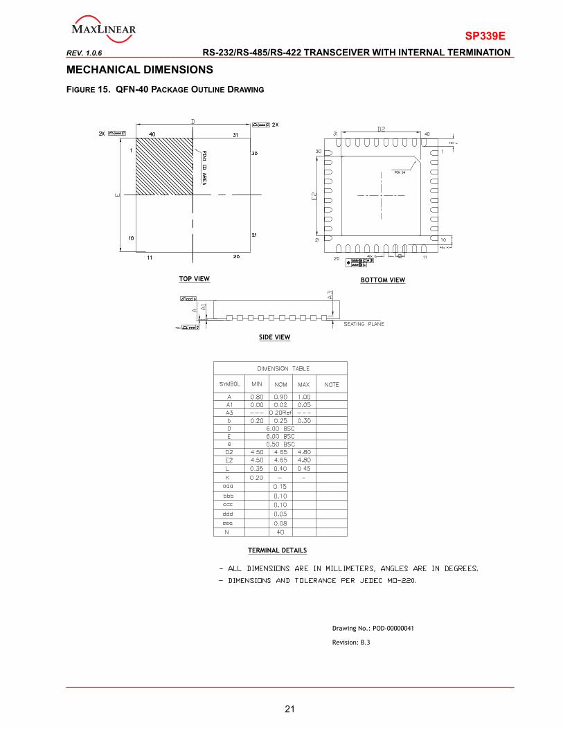
MECHANICAL DIMENSIONSFIGURE 15. QFN-40 PACKAGE OUTLINE DRAWING
Revision: B.3
Drawing No.: POD-00000041
TOP VIEW
TERMINAL DETAILS
SIDE VIEW
BOTTOM VIEW
SP339E
22
RS-232/RS-485/RS-422 TRANSCEIVER WITH INTERNAL TERMINATION REV. 1.0.6
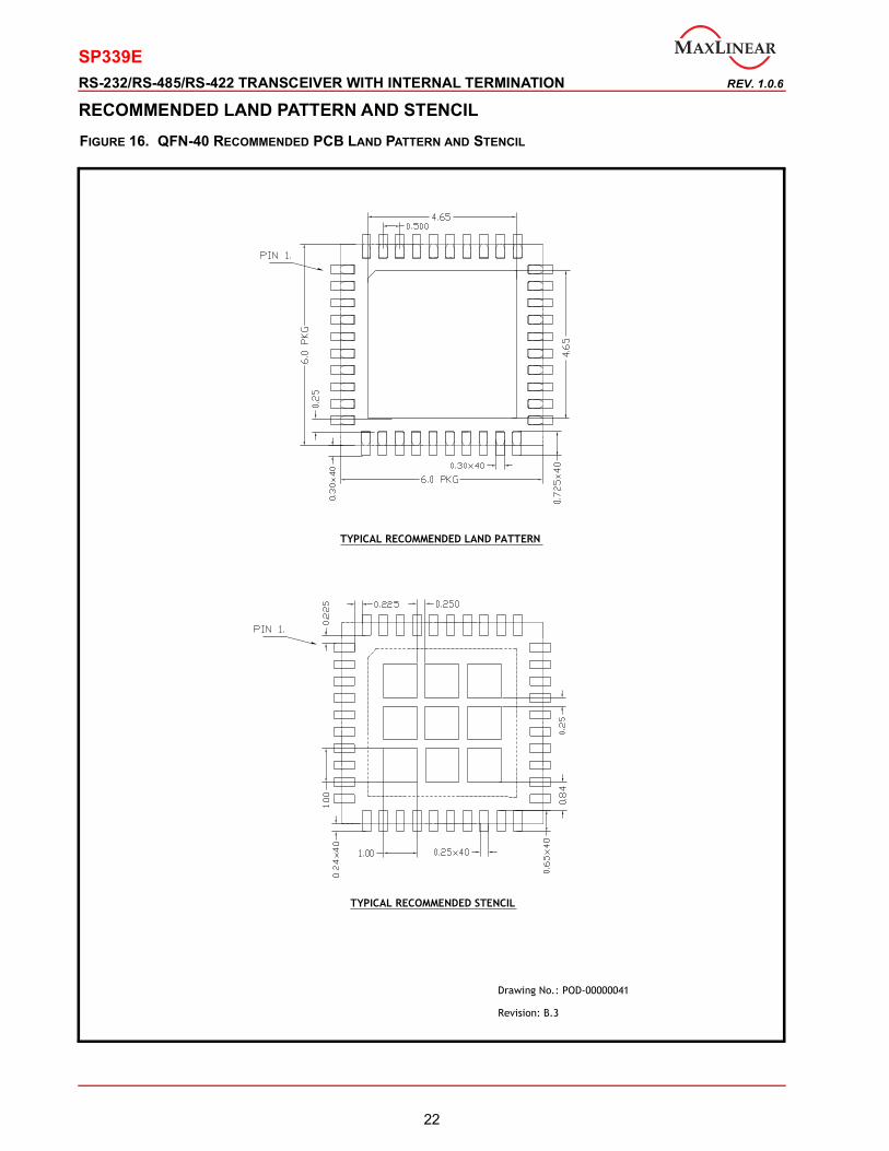
RECOMMENDED LAND PATTERN AND STENCILFIGURE 16. QFN-40 RECOMMENDED PCB LAND PATTERN AND STENCIL
Revision: B.3
Drawing No.: POD-00000041
TYPICAL RECOMMENDED STENCIL
TYPICAL RECOMMENDED LAND PATTERN

SP339E
23
REV. 1.0.6 RS-232/RS-485/RS-422 TRANSCEIVER WITH INTERNAL TERMINATION
FIGURE 17. PIN 1 ORIENTATION IN TAPE

24
The content of this document is furnished for informational use only, is subject to change without notice, and should not be construed as a commitment by MaxLinear, Inc. MaxLinear,Inc. assumes no responsibility or liability for any errors or inaccuracies that may appear in the informational content contained in this guide. Complying with all applicable copyright lawsis the responsibility of the user. Without limiting the rights under copyright, no part of this document may be reproduced into, stored in, or introduced into a retrieval system, or transmittedin any form or by any means (electronic, mechanical, photocopying, recording, or otherwise), or for any purpose, without the express written permission of MaxLinear, Inc. Maxlinear, Inc. does not recommend the use of any of its products in life support applications where the failure or malfunction of the product can reasonably be expected to cause failureof the life support system or to significantly affect its safety or effectiveness. Products are not authorized for use in such applications unless MaxLinear, Inc. receives, in writing,assurances to its satisfaction that: (a) the risk of injury or damage has been minimized; (b) the user assumes all such risks; (c) potential liability of MaxLinear, Inc. is adequately protectedunder the circumstances. MaxLinear, Inc. may have patents, patent applications, trademarks, copyrights, or other intellectual property rights covering subject matter in this document. Except as expresslyprovided in any written license agreement from MaxLinear, Inc., the furnishing of this document does not give you any license to these patents, trademarks, copyrights, or otherintellectual property. MaxLinear, the MaxLinear logo, and any MaxLinear trademarks, MxL, Full-Spectrum Capture, FSC, G.now, AirPHY and the MaxLinear logo are all on the products sold, are alltrademarks of MaxLinear, Inc. or one of MaxLinear’s subsidiaries in the U.S.A. and other countries. All rights reserved. Other company trademarks and product names appearing hereinare the property of their respective owners. © 2011 - 2019 MaxLinear, Inc. All rights reserved.
SP339EREV. 1.0.6 RS-232/RS-485/RS-422 TRANSCEIVER WITH INTERNAL TERMINATION
Corporate Headquarters:5966 LaPlace CourtSuite 100Carlsbad, CA 92008Tel.:+1 (760) 692-0711Fax:+1 (760) 444-8598www.maxlinear.com
REVISION HISTORY
DATE REVISION DESCRIPTION
October 2011 1.0.0 Production Release
December 2011 1.0.1Added CL and RL test conditions to figures 13 and 14 on page 9Absolute max rating ±18V on page 2Text edits in product summary on page 19
February 2013 1.0.2Clarified test conditions for Driver Output Leakage Current on page 7Added ±15kV Air Gap ESD per PCN 12-1009-01Added ±4kV HBM ESD to non-bus pins per PCN 12-1009-01
November 2013 1.0.3 Added recommended PCB land pattern drawing.
December 2013 1.0.4Combined QFN-40 package outline drawing and recommended PCB land pattern in Figure 16. Added table for ”Suggested DB9 Connector Pinout” on page 5 and Figure 17 for pin 1 orientation in tape.
February 2018 1.0.5Update to MaxLinear logo. Update format and Ordering Information. Corrected typo for pin 28, Mode 11 in Pin Description. Moved ESD ratings on page 2.
January 2019 1.0.6 Corrected typo in recommended stencil. Updated Ordering Information.