SP3082E/ SP3083E/ SP3084E/ SP3085E/ SP3088E Data Sheet ... · conditions over the entire...
35
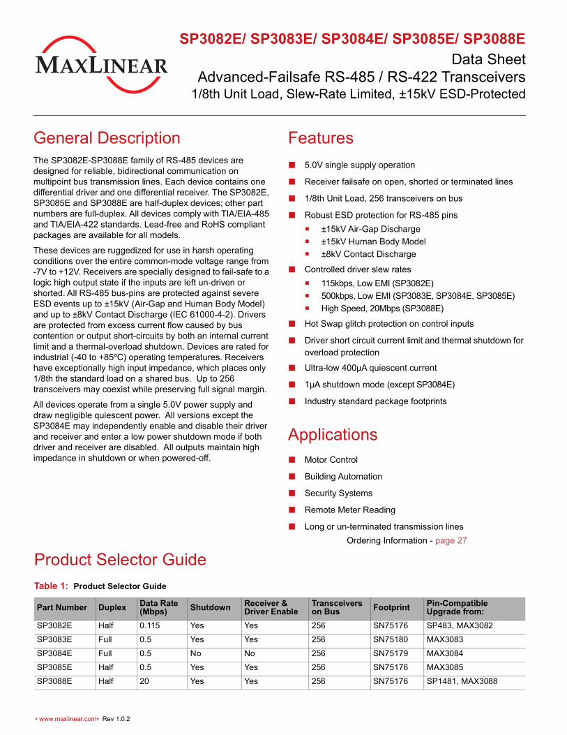
• www.maxlinear.com• Rev 1.0.2 SP3082E/ SP3083E/ SP3084E/ SP3085E/ SP3088E Data Sheet Advanced-Failsafe RS-485 / RS-422 Transceivers 1/8th Unit Load, Slew-Rate Limited, ±15kV ESD-Protected General Description The SP3082E-SP3088E family of RS-485 devices are designed for reliable, bidirectional communication on multipoint bus transmission lines. Each device contains one differential driver and one differential receiver. The SP3082E, SP3085E and SP3088E are half-duplex devices; other part numbers are full-duplex. All devices comply with TIA/EIA-485 and TIA/EIA-422 standards. Lead-free and RoHS compliant packages are available for all models. These devices are ruggedized for use in harsh operating conditions over the entire common-mode voltage range from -7V to +12V. Receivers are specially designed to fail-safe to a logic high output state if the inputs are left un-driven or shorted. All RS-485 bus-pins are protected against severe ESD events up to ±15kV (Air-Gap and Human Body Model) and up to ±8kV Contact Discharge (IEC 61000-4-2). Drivers are protected from excess current flow caused by bus contention or output short-circuits by both an internal current limit and a thermal-overload shutdown. Devices are rated for industrial (-40 to +85ºC) operating temperatures. Receivers have exceptionally high input impedance, which places only 1/8th the standard load on a shared bus. Up to 256 transceivers may coexist while preserving full signal margin. All devices operate from a single 5.0V power supply and draw negligible quiescent power. All versions except the SP3084E may independently enable and disable their driver and receiver and enter a low power shutdown mode if both driver and receiver are disabled. All outputs maintain high impedance in shutdown or when powered-off. Features ■ 5.0V single supply operation ■ Receiver failsafe on open, shorted or terminated lines ■ 1/8th Unit Load, 256 transceivers on bus ■ Robust ESD protection for RS-485 pins ±15kV Air-Gap Discharge ±15kV Human Body Model ±8kV Contact Discharge ■ Controlled driver slew rates 115kbps, Low EMI (SP3082E) 500kbps, Low EMI (SP3083E, SP3084E, SP3085E) High Speed, 20Mbps (SP3088E) ■ Hot Swap glitch protection on control inputs ■ Driver short circuit current limit and thermal shutdown for overload protection ■ Ultra-low 400μA quiescent current ■ 1μA shutdown mode (except SP3084E) ■ Industry standard package footprints Applications ■ Motor Control ■ Building Automation ■ Security Systems ■ Remote Meter Reading ■ Long or un-terminated transmission lines Ordering Information - page 27 Product Selector Guide Table 1: Product Selector Guide Part Number Duplex Data Rate (Mbps) Shutdown Receiver & Driver Enable Transceivers on Bus Footprint Pin-Compatible Upgrade from: SP3082E Half 0.115 Yes Yes 256 SN75176 SP483, MAX3082 SP3083E Full 0.5 Yes Yes 256 SN75180 MAX3083 SP3084E Full 0.5 No No 256 SN75179 MAX3084 SP3085E Half 0.5 Yes Yes 256 SN75176 MAX3085 SP3088E Half 20 Yes Yes 256 SN75176 SP1481, MAX3088
Transcript of SP3082E/ SP3083E/ SP3084E/ SP3085E/ SP3088E Data Sheet ... · conditions over the entire...
• www.maxlinear.com• Rev 1.0.2
SP3082E/ SP3083E/ SP3084E/ SP3085E/ SP3088EData Sheet
Advanced-Failsafe RS-485 / RS-422 Transceivers1/8th Unit Load, Slew-Rate Limited, ±15kV ESD-Protected
General DescriptionThe SP3082E-SP3088E family of RS-485 devices are designed for reliable, bidirectional communication on multipoint bus transmission lines. Each device contains one differential driver and one differential receiver. The SP3082E, SP3085E and SP3088E are half-duplex devices; other part numbers are full-duplex. All devices comply with TIA/EIA-485 and TIA/EIA-422 standards. Lead-free and RoHS compliant packages are available for all models.
These devices are ruggedized for use in harsh operating conditions over the entire common-mode voltage range from -7V to +12V. Receivers are specially designed to fail-safe to a logic high output state if the inputs are left un-driven or shorted. All RS-485 bus-pins are protected against severe ESD events up to ±15kV (Air-Gap and Human Body Model) and up to ±8kV Contact Discharge (IEC 61000-4-2). Drivers are protected from excess current flow caused by bus contention or output short-circuits by both an internal current limit and a thermal-overload shutdown. Devices are rated for industrial (-40 to +85ºC) operating temperatures. Receivers have exceptionally high input impedance, which places only 1/8th the standard load on a shared bus. Up to 256 transceivers may coexist while preserving full signal margin.
All devices operate from a single 5.0V power supply and draw negligible quiescent power. All versions except the SP3084E may independently enable and disable their driver and receiver and enter a low power shutdown mode if both driver and receiver are disabled. All outputs maintain high impedance in shutdown or when powered-off.
Features 5.0V single supply operation
Receiver failsafe on open, shorted or terminated lines
1/8th Unit Load, 256 transceivers on bus
Robust ESD protection for RS-485 pins ±15kV Air-Gap Discharge ±15kV Human Body Model ±8kV Contact Discharge
Controlled driver slew rates 115kbps, Low EMI (SP3082E) 500kbps, Low EMI (SP3083E, SP3084E, SP3085E) High Speed, 20Mbps (SP3088E)
Hot Swap glitch protection on control inputs
Driver short circuit current limit and thermal shutdown for overload protection
Ultra-low 400μA quiescent current
1μA shutdown mode (except SP3084E)
Industry standard package footprints
Applications Motor Control
Building Automation
Security Systems
Remote Meter Reading
Long or un-terminated transmission linesOrdering Information - page 27
Product Selector GuideTable 1: Product Selector Guide
Part Number Duplex Data Rate (Mbps) Shutdown Receiver &
Driver EnableTransceivers on Bus Footprint Pin-Compatible
Upgrade from:SP3082E Half 0.115 Yes Yes 256 SN75176 SP483, MAX3082SP3083E Full 0.5 Yes Yes 256 SN75180 MAX3083SP3084E Full 0.5 No No 256 SN75179 MAX3084SP3085E Half 0.5 Yes Yes 256 SN75176 MAX3085SP3088E Half 20 Yes Yes 256 SN75176 SP1481, MAX3088

SP3082E/ SP3083E/ SP3084E/ SP3085E/ SP3088E Data Sheet Revision History
8/29/19 Rev 1.0.2 ii
Revision HistoryDocument No. Release Date Change DescriptionM 2/22/07 Legacy Sipex Datasheet.1.0.0 06/23/09 Convert to Exar format and change revision to 1.0.0.1.0.1 08/26/11 Correct type error to Vcc range on page 4 from Vcc = 5.0V +/-5% to Vcc = 5.0V +/-10%. Add +/
-65V transient over voltage tolerance to ABS Maximum Ratings and add Figure 11 test circuit.1.0.2 8/29/19 Update to MaxLinear format, update Ordering Information. Move Pin Information section to just
before Detailed Description section, ESD Ratings to below Absolute Maximum Ratings section, and Product Selector Guide to page 1. Correct Half Duplex Network Typical Application. Removed obsolete SP3080E, SP3081E, SP3086E and SP3087E.

SP3082E/ SP3083E/ SP3084E/ SP3085E/ SP3088E Data Sheet Table of Contents
8/29/19 Rev 1.0.2 iii
Table of ContentsGeneral Description............................................................................................................................................. iFeatures............................................................................................................................................................... iApplications ......................................................................................................................................................... iProduct Selector Guide....................................................................................................................................... iDevice Architecture and Block Diagrams ........................................................................................................ 1
14-pin Full Duplex: ....................................................................................................................................................... 1
8-pin Full Duplex: ......................................................................................................................................................... 1
8-pin Half Duplex: ......................................................................................................................................................... 1
Specifications ..................................................................................................................................................... 2Absolute Maximum Ratings...........................................................................................................................................2
ESD Ratings ..................................................................................................................................................................2
Recommended Operating Conditions ...........................................................................................................................3
Electrical Characteristics ...............................................................................................................................................4
Timing Characteristics ...................................................................................................................................................5
Typical Performance Characteristics................................................................................................................ 7
Test Circuits and Timing Diagrams................................................................................................................. 15
Function Tables ................................................................................................................................................ 20
Pin Information ................................................................................................................................................. 21Pin Configurations .......................................................................................................................................................21
Pin Descriptions ..........................................................................................................................................................21
Detailed Description ......................................................................................................................................... 22Receiver Input Filtering .............................................................................................................................................. 22
Advanced Fail Safe .................................................................................................................................................... 22
Hot-Swap Capability ................................................................................................................................................... 22
±15kV ESD Protection................................................................................................................................................ 22
ESD Test Conditions .................................................................................................................................................. 23
IEC 61000-4-2 ............................................................................................................................................................ 23
Machine Model ........................................................................................................................................................... 23
256 Transceivers on the Bus...................................................................................................................................... 23
Low Power Shutdown Mode....................................................................................................................................... 23
Driver Output Protection ............................................................................................................................................. 23
Line Length, EMI and Reflections .............................................................................................................................. 23
Typical Applications.................................................................................................................................................... 24

SP3082E/ SP3083E/ SP3084E/ SP3085E/ SP3088E Data Sheet Table of Contents
8/29/19 Rev 1.0.2 iv
Mechanical Dimensions ................................................................................................................................... 25NSOIC8 .......................................................................................................................................................................25
Mechanical Dimensions ................................................................................................................................... 26NSOIC14 .....................................................................................................................................................................26
Ordering Information........................................................................................................................................ 27
SP3082E/ SP3083E/ SP3084E/ SP3085E/ SP3088E Data Sheet List of Figures
8/29/19 Rev 1.0.2 v
List of FiguresFigure 1: 14-pin Full Duplex.................................................................................................................................. 1
Figure 2: 8-pin Full Duplex.................................................................................................................................... 1
Figure 3: 8-pin Half Duplex ................................................................................................................................... 1
Figure 4: No-Load Supply Current vs. Temperature............................................................................................. 7
Figure 5: Shutdown Current vs. Temperature ...................................................................................................... 7
Figure 6: Supply Current vs. Signaling Rate (SP3082E) ...................................................................................... 7
Figure 7: Supply Current vs. Signaling Rate (SP3083E, - SP3085E)................................................................... 7
Figure 8: Supply Current vs. Signaling Rate (SP3088E) ...................................................................................... 7
Figure 9: Output Current vs. Driver Output Low Voltage ...................................................................................... 7
Figure 10: Output Current vs. Driver Output High Voltage ................................................................................... 8
Figure 11: Driver Output Current vs. Differential Output Voltage ......................................................................... 8
Figure 12: Driver Differential Output Voltage vs. Temperature............................................................................. 8
Figure 13: Receiver Output Low Voltage vs. Temperature................................................................................... 8
Figure 14: Receiver Output High Voltage vs. Temperature.................................................................................. 8
Figure 15: Receiver Output Voltage vs. Differential Input Voltage ....................................................................... 8
Figure 16: Output Current vs. Receiver Output Low Voltage ............................................................................... 9
Figure 17: Driver Average Propagation Delay vs. Temperature (SP3082E) ........................................................ 9
Figure 18: Driver Propagation Delay vs. Temperature (SP3082E)....................................................................... 9
Figure 19: Driver Average Propagation Delay vs. Temperature (SP3083E - SP3085E)...................................... 9
Figure 20: Output Current vs. Receiver Output High Voltage............................................................................... 9
Figure 21: Driver Propagation Delay vs. Temperature (SP3083E - SP3085E) .................................................... 9
Figure 22: Driver Propagation Delay vs. Temperature (SP3088E)..................................................................... 10
Figure 23: Receiver Average Propagation Delay vs.Temperature (SP3082E)................................................... 10
Figure 24: Receiver Propagation Delay vs. Temperature (SP3082E) ................................................................ 10
Figure 25: Receiver Propagation Delay vs. Temperature (SP3083E - SP3085E).............................................. 10
Figure 26: Driver Average Propagation Delay vs. Temperature (SP3088E) ...................................................... 10
Figure 27: Receiver Propagation Delay vs. Temperature (SP3088E) ................................................................ 10
Figure 28: Driver Propagation Delay (SP3082E)................................................................................................ 11
Figure 29: Driver and Receiver Hot Swap Performance vs. VCC ....................................................................... 11
Figure 30: Receiver Average Propagation Delay vs. Temperature (SP3088E).................................................. 11
Figure 31: Driver Output Waveform Low to High (SP3082E) ............................................................................. 11
Figure 32: Driver Output Waveform High to Low (SP3082E) ............................................................................. 11
Figure 33: Driver and Receiver Waveform High to Low (SP3082E)................................................................... 12
SP3082E/ SP3083E/ SP3084E/ SP3085E/ SP3088E Data Sheet List of Figures
8/29/19 Rev 1.0.2 vi
Figure 34: Driver Propagation Delay (SP3083E - SP3085E) ............................................................................. 12
Figure 35: Driver Output Waveform Low to High (SP3083E - SP3085E)........................................................... 12
Figure 36: Driver Output Waveform High to Low (SP3083E - SP3085E)........................................................... 12
Figure 37: Driver and Receiver Waveform Low to High (SP3082E)................................................................... 12
Figure 38: Driver and Receiver Waveform Low to High (SP3083E - SP3085E) ................................................ 12
Figure 39: Driver Propagation Delay (SP3088E)................................................................................................ 13
Figure 40: Driver Output Waveform Low to High (SP3088E) ............................................................................. 13
Figure 41: Driver Output Waveform High to Low (SP3088E) ............................................................................. 13
Figure 42: Driver and Receiver Waveform Low to High (SP3088E)................................................................... 13
Figure 43: Driver and Receiver Waveform High to Low (SP3083E - SP3085E) ................................................ 13
Figure 44: Driver and Receiver Waveform High to Low (SP3088E)................................................................... 13
Figure 45: Receiver Propagation Delay (SP3088E) ........................................................................................... 14
Figure 46: Receiver Propagation Delay (SP3082E) ........................................................................................... 14
Figure 47: Receiver Propagation Delay (SP3083E - SP3085E)......................................................................... 14
Figure 48: Driver DC Test Circuit........................................................................................................................ 15
Figure 49: Receiver DC Test Circuit ................................................................................................................... 15
Figure 50: Driver Propagation Delay Time Test Circuit and Timing Diagram..................................................... 15
Figure 51: Driver Short Circuit Current Limit Test Circuit ................................................................................... 16
Figure 52: Driver Differential Output Test Circuit................................................................................................ 16
Figure 53: Driver Enable and Disable Times Test Circuit and Timing Diagram ................................................. 16
Figure 54: Driver Enable and Disable Times Test Circuit and Timing Diagram ................................................. 17
Figure 55: Receiver Propagation Delay Test Circuit and Timing Diagram ......................................................... 17
Figure 56: Receiver Enable and Disable Times Test Circuit .............................................................................. 18
Figure 57: Receiver Enable and Disable Timing Diagram.................................................................................. 18
Figure 58: Transient Over Voltage Tolerance Test Circuit ................................................................................. 19
Figure 59: Pin Configurations ............................................................................................................................. 21
Figure 60: Half-Duplex Network.......................................................................................................................... 24
Figure 61: Bi-Directional Full-Duplex Network.................................................................................................... 24
Figure 62: Point to Multi-Point Repeater............................................................................................................. 24
Figure 63: Mechanical Dimension, NSOIC8....................................................................................................... 25
Figure 64: Mechanical Dimensions, NSOIC14 ................................................................................................... 26

SP3082E/ SP3083E/ SP3084E/ SP3085E/ SP3088E Data Sheet List of Tables
8/29/19 Rev 1.0.2 vii
List of TablesTable 1: Product Selector Guide............................................................................................................................ i
Table 1: Absolute Maximum Ratings .................................................................................................................... 2
Table 2: ESD Ratings ........................................................................................................................................... 2
Table 3: Recommended Operating Conditions..................................................................................................... 3
Table 4: Electrical Characteristics ........................................................................................................................ 4
Table 5: SP3082E Driver Characteristics ............................................................................................................. 5
Table 6: SP3083E, SP3084E, SP3085E Driver Characteristics........................................................................... 5
Table 7: SP3088E Driver Characteristics ............................................................................................................. 6
Table 8: Receiver Characteristics......................................................................................................................... 6
Table 9: SP3083E (Full Duplex) ......................................................................................................................... 20
Table 10: SP3083E (Full Duplex) ....................................................................................................................... 20
Table 11: SP3084E (Full Duplex) ....................................................................................................................... 20
Table 12: SP3084E (Full Duplex) ....................................................................................................................... 20
Table 13: SP3082E, SP3085E, SP3088E (Half Duplex) .................................................................................... 20
Table 14: SP3082E, SP3085E, SP3088E (Half Duplex) .................................................................................... 20
Table 15: Pin Descriptions.................................................................................................................................. 21
Table 16: Ordering Information........................................................................................................................... 27

SP3082E/ SP3083E/ SP3084E/ SP3085E/ SP3088E Data Sheet Device Architecture and Block Diagrams
8/29/19 Rev 1.0.2 1
Device Architecture and Block DiagramsDevices are available in three industry standard architectures and footprints. In each footprint, there are three speed grades available.
Figure 2: 14-pin Full Duplex
Figure 3: 8-pin Full Duplex
Figure 4: 8-pin Half Duplex
14-pin Full Duplex:SP3083E, 500kbps slew limited
8-pin Full Duplex:SP3084E, 500kbps slew limited
8-pin Half Duplex:SP3082E, 115kbps slew limited
SP3085E, 500kbps slew limited
SP3088E, 20Mbps
Vcc
D
R
NCAB
Z
Y
RO
NC
NC
DERE
GNDGND
2
1
34
567 8
9
10
11121314
DI
D
RAB
Z
Y
RO
GND
2
1
34 5
6
78
DI
Vcc
D
R
AB
RO
GND
2
1
3
45
67
8
DE
VCC
RE
DI

SP3082E/ SP3083E/ SP3084E/ SP3085E/ SP3088E Data Sheet Specifications
8/29/19 Rev 1.0.2 2
Specifications
Absolute Maximum RatingsImportant: These are stress ratings only and functional operation of the device at these ratings or any other above those indicated in the operation sections of the specifications below is not implied. Exposure to absolute maximum rating conditions for extended periods of time may affect reliability.
ESD Ratings
Table 1: Absolute Maximum Ratings
Parameter Minimum Maximum UnitsSupply voltage VCC 7.0 V
Input voltage at control input pins (RE, DE) –0.3 VCC+ 0.3 V
Driver input voltage (DI) –0.3 VCC+ 0.3 V
Driver output voltage (A, B, Y & Z) –13 13 V
Receiver output voltage (RO) –0.3 VCC+ 0.3 V
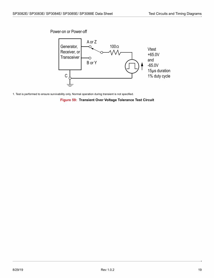
Receiver input voltage (A, B) –13 13 VVoltage input range, transient pulse, A, B, Y and Z through 100Ω, see Figure 59 -65 65 V
Package Power DissipationMaximum junction temperature 150 °C8-pin SO ѲJA 128.4 °C/W
14-pin SO ѲJA 86 °C/W
Operating Temperature RangesStorage temperature range –65 150 °CLead temperature (soldering, 10s) 300 °C
Table 2: ESD Ratings
Parameter Limit UnitsHBM - Human Body Model (pins A, B, Y & Z) ±15 kVHBM - Human Body Model (pins RO, DI, DE) ±2 kVIEC 1000-4-2 Airgap Discharge (pins Y, Z, A & B) ±15 kVIEC 1000-4-2 Contact Discharge (pins Y, Z, A & B) ±8 kV
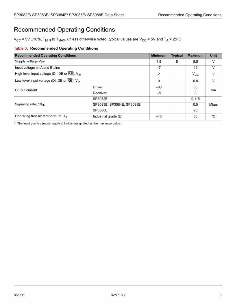
SP3082E/ SP3083E/ SP3084E/ SP3085E/ SP3088E Data Sheet Recommended Operating Conditions
8/29/19 Rev 1.0.2 3
Recommended Operating ConditionsVCC = 5V ±10%, TMIN to TMAX, unless otherwise noted, typical values are VCC = 5V and TA = 25°C
1. The least positive (most negative) limit is designated as the maximum value.
Table 3: Recommended Operating Conditions
Recommended Operating Conditions Minimum Typical Maximum UnitSupply voltage VCC 4.5 5 5.5 V
Input voltage on A and B pins –7 12 V
High-level input voltage (DI, DE or RE), VIH 2 VCC V
Low-level input voltage (DI, DE or RE), VIH 0 0.8 V
Output currentDriver –60 60
mAReceiver –8 8
Signaling rate, 1/tUI
SP3082E 0.115MbpsSP3083E, SP3084E, SP3085E 0.5
SP3088E 20Operating free air temperature, TA Industrial grade (E) –40 85 °C

SP3082E/ SP3083E/ SP3084E/ SP3085E/ SP3088E Data Sheet Electrical Characteristics
8/29/19 Rev 1.0.2 4
Electrical CharacteristicsTable 4: Electrical Characteristics
Parameter Test Condition Minimum Typical Maximum Units
Digital Input Signals: DI, DE, RE
Logic input thresholdsHigh, VIH 2.0
VLow, VIL 0.8
Logic input current TA = 25°C, after first transition ±1 µA
Input hysteresis TA = 25°C 100 mV
Driver
Differential driver output (VOD) No load VCC V
Differential driver output, Test 1RL= 100Ω (RS-422) 2 VCC
VRL= 54Ω (RS-485) 1.5 2.7 VCC
Differential driver output, Test 2 VCM = -7 to +12V 1.5 VCC V
Change in magnitude of differential output voltage (∆VOD)(1) RL= 54Ω or 100Ω ±0.2 V
Driver common mode output voltage (VCC) RL= 54Ω or 100Ω 1 3 V
Change in common mode output voltage (∆VOC) RL= 54Ω or 100Ω ±0.2 uA
Driver short circuit current limit -7V ≤ VOUT ≤ 12V(5) ±250 mA
Output leakage current (Full-duplex versions, Y & Z pins)(2)
DE = 0, RE = 0,VCC = 0 or 5.5V
VOUT = 12V 125µA
VOUT = -7V –100
Receiver
Receiver input resistance -7V ≤ VCM ≤ 12V 96 kΩ
Input current (A, B pins)DE = 0, RE = 0VCC = 0 or 5.5V
VIN = 12V 125µA
VIN = -7V –100
Receiver differential threshold (VA - VB) -7V ≤ VCM ≤ 12V –200 –125 –40 mV
Receiver input hysteresis 25 mV
Receiver output voltageVOH IOUT = -8mA, VID = -40mV VCC - 1.5
VVOL IOUT = -8mA, VID = -200mV 0.4
High-Z receiver output current VCC = 5.5V, 0 ≤ VOUT ≤ VCC ±1 µA
Receiver output short circuit current 0 ≤ VRO ≤ VCC ±95 mA

SP3082E/ SP3083E/ SP3084E/ SP3085E/ SP3088E Data Sheet Switching Characteristics
8/29/19 Rev 1.0.2 5
1. Change in magnitude of differential output voltage and change in magnitude of common mode output voltage are the changes in output voltage when DI input changes state.
2. Except devices which don’t have DE or RE inputs.
3. The transceivers are put into shutdown by bringing RE high and DE low. If the inputs are in this state for less than 50ns, the device does not enter shutdown. If the enable inputs are held in this state for at least 600ns, the device is assured to be in shutdown. In this low power mode, most circuitry is disabled and supply current is typically 1nA.
4. Characterized, not 100% tested.
5. See Figure 52.
Timing CharacteristicsUnless otherwise noted, VCC = 5.0 ±0.5V, ambient temperature TA from -40 to 85°C.
Supply and Protection
Supply current
IQ, active mode
No load, DI = 0 or VCC 400 900 µA
Shutdown mode
DE = 0, RE = VCC, DI = VCC 1 µA
Thermal shutdown temperature Junction temperature 165°C
Thermal shutdown hysteresis 15
Table 5: SP3082E Driver Characteristics
Driver Characteristics Conditions Minimum Typical Maximum UnitData signaling rate (1 / tUI) Duty cycle 40 to 60% 115 kbps
Driver propagation delay (tPHL, tPLH)
RL = 54Ω, CL = 50pF
500 2600 ns
Driver output rise / fall time (tR, tF) 667 1200 2500 ns
Driver differential skew (tPLH - tPHL) ±200 ns
Shutdown to driver output valid (tDZV) 6000 ns
Table 6: SP3083E, SP3084E, SP3085E Driver Characteristics
Driver Characteristics Conditions Minimum Typical Maximum UnitData signaling rate (1 / tUI) Duty cycle 40 to 60% 500 kbps
Driver propagation delay (tPHL, tPLH)
RL = 54Ω, CL = 50pF
250 1000 ns
Driver output rise / fall time (tR, tF) 200 530 750 ns
Driver differential skew (tPLH - tPHL) ±100 ns
Driver enable to output high (tDZH)
SP3083E, SP3084E
2500 ns
Driver enable to output low (tDZL) 2500 ns
Driver disable from output high (tDHZ) 100 ns
Driver disable from output low (tDLZ) 100 ns
Shutdown to driver output valid (tDZV) 4500 ns
Table 4: Electrical Characteristics
Parameter Test Condition Minimum Typical Maximum Units

SP3082E/ SP3083E/ SP3084E/ SP3085E/ SP3088E Data Sheet Switching Characteristics
8/29/19 Rev 1.0.2 6
Table 7: SP3088E Driver Characteristics
Receiver Characteristics Conditions Minimum Typical Maximum UnitData signaling rate (1 / tUI) Duty cycle 40 to 60% 20 Mbps
Driver propagation delay (tPHL, tPLH)
RL = 54Ω, CL = 50pF
12 20 ns
Driver output rise / fall time (tR, tF) 6 10 ns
Driver differential skew (tPLH - tPHL) ±5 ns
Shutdown to driver output valid (tDZV) 250 ns
Table 8: Receiver Characteristics
Receiver Characteristic Conditions Minimum Typical Maximum UnitReceiver prop. delay SP3082E - SP3085E
CL = 15pF, VID = ±2V
75 200 nsReceiver prop. delay SP3088E 75 nsProp. delay skew SP3082E - SP3085E ±30 nsProp. delay skew SP3088E ±5 ns
Receiver output rise / fall time CL = 15pF 15 ns
Receiver enable to output high (tZH) 50 ns
Receiver enable from output low (tZL) 50 ns
Receiver disable from high (tHZ) 50 ns
Receiver disable from low (tLZ) 50 ns
Shutdown to receiver output valid (tROV) 3500 ns
Time to shutdown(2, 3, 4) 50 200 600 ns
SP3082E/ SP3083E/ SP3084E/ SP3085E/ SP3088E Data Sheet Typical Performance Characteristics
8/29/19 Rev 1.0.2 7
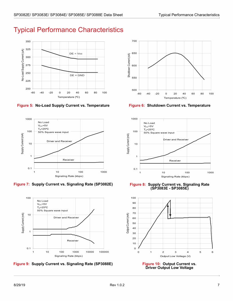
Typical Performance Characteristics
Figure 5: No-Load Supply Current vs. Temperature Figure 6: Shutdown Current vs. Temperature
200
225
250
275
300
325
350
-60 -40 -20 0 20 40 60 80 100
Temperature (ºC)
No-L
oad
Supp
ly Cu
rrent
(uA)
DE = Vcc
DE = GND
500
550
600
650
700
-60 -40 -20 0 20 40 60 80 100
Temperature (ºC)
Shut
down
Cur
rent
(nA)
Figure 7: Supply Current vs. Signaling Rate (SP3082E) Figure 8: Supply Current vs. Signaling Rate (SP3083E - SP3085E)
0.1
1
10
100
1000
1 10 100 1000
Signaling Rate (kbps)
Supp
ly Cu
rrent
(mA)
Driver and Receiver
Receiver
No LoadVCC=5VTA=25ºC50% Square wave input
0.1
1
10
100
1000
1 10 100 1000
Signaling Rate (kbps)
Supp
ly Cu
rrent
(mA)
Receiver
Driver and Receiver
No LoadVCC=5VTA=25ºC50% Square wave input
Figure 9: Supply Current vs. Signaling Rate (SP3088E) Figure 10: Output Current vs. Driver Output Low Voltage
0.1
1
10
100
1 10 100 1000 10000 100000
Signaling Rate (kbps)
Supp
ly Cu
rrent
(mA)
Receiver
Driver and Receiver
No LoadVCC=5VTA=25ºC50% Square wave input
0
10
20
30
40
50
60
70
80
90
100
0 1 2 3 4 5 6
Output Low Voltage (V)
Outpu
t Cur
rent
(mA)

SP3082E/ SP3083E/ SP3084E/ SP3085E/ SP3088E Data Sheet Typical Performance Characteristics
8/29/19 Rev 1.0.2 8
Figure 11: Output Current vs. Driver Output High Voltage
Figure 12: Driver Output Current vs. Differential Output Voltage
-120
-100
-80
-60
-40
-20
0-2 0 2 4 6
Output High Voltage (V)
Outpu
t Cur
rent
(mA)
0.01
0.1
1
10
100
0 1 2 3 4 5 6
Differential Output Voltage (V)
Outpu
t Cur
rent
(mA)
Figure 13: Driver Differential Output Voltage vs. Temperature
Figure 14: Receiver Output Low Voltage vs. Temperature
2
2.2
2.4
2.6
2.8
3
3.2
3.4
-60 -40 -20 0 20 40 60 80 100
Temperature (ºC)
Outpu
t Volt
age
(V)
RL=54
RL =100
0.1
0.15
0.2
0.25
0.3
0.35
-60 -40 -20 0 20 40 60 80 100
Temperature (ºC)
Outpu
t Low
Volt
age (
V)IOUT=8mA, VID=-200mV
Figure 15: Receiver Output High Voltage vs. Temperature
Figure 16: Receiver Output Voltage vs. Differential Input Voltage
3.5
3.6
3.7
3.8
3.9
4
-60 -40 -20 0 20 40 60 80 100
Temperature (ºC)
Outpu
t High
Volt
age (
V)
IOUT=8mA, VID=-40mV
0
1
2
3
4
5
-200 -180 -160 -140 -120 -100 -80 -60 -40 -20 0
Differential Input Voltage (mV)
Rece
iver O
utput
Volt
age
(V)
VCC=5VTA=25ºC
SP3082E/ SP3083E/ SP3084E/ SP3085E/ SP3088E Data Sheet Typical Performance Characteristics
8/29/19 Rev 1.0.2 9
Figure 17: Output Current vs. Receiver Output Low Voltage
Figure 18: Driver Average Propagation Delay vs. Temperature (SP3082E)
0
10
20
30
40
50
60
0 1 2 3 4 5
Output Low Voltage (V)
Outpu
t Curr
ent (m
A)
870
880
890
900
910
920
930
940
950
960
-60 -40 -20 0 20 40 60 80 100
Temperature (ºC)
Prop
agati
on D
elay (
ns)
RL=54 ,CL=50pF
Figure 19: Driver Propagation Delay vs. Temperature (SP3082E)
Figure 20: Driver Average Propagation Delay vs. Temperature (SP3083E - SP3085E)
870
880
890
900
910
920
930
940
950
960
-60 -40 -20 0 20 40 60 80 100
Temperature (ºC)
Prop
agat
ion
Dela
y (ns
)
tPLH
tPHL
RL=54 ,CL=50pF
410
415
420
425
430
435
-60 -40 -20 0 20 40 60 80 100
Temperature (ºC)
Prop
agati
on D
elay (
ns)
RL=54 ,CL=50pF
Figure 21: Output Current vs. Receiver Output High Voltage
Figure 22: Driver Propagation Delay vs. Temperature (SP3083E - SP3085E)
0
5
10
15
20
25
30
35
0 1 2 3 4 5
Output High Voltage (V)
Outpu
t Cur
rent
(mA)
390
400
410
420
430
440
450
460
-60 -40 -20 0 20 40 60 80 100
Temperature (ºC)
Prop
agati
on D
elay (
ns)
tPLH
tPHL
RL=54 ,CL=50pF
SP3082E/ SP3083E/ SP3084E/ SP3085E/ SP3088E Data Sheet Typical Performance Characteristics
8/29/19 Rev 1.0.2 10
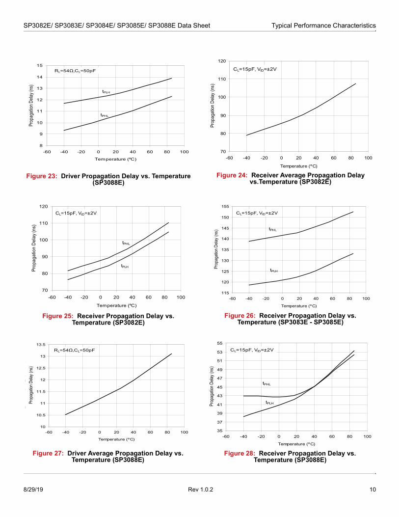
Figure 23: Driver Propagation Delay vs. Temperature (SP3088E)
Figure 24: Receiver Average Propagation Delay vs.Temperature (SP3082E)
8
9
10
11
12
13
14
15
-60 -40 -20 0 20 40 60 80 100
Temperature (ºC)
Prop
agati
on D
elay (
ns)
tPLH
tPHL
RL=54 ,CL=50pF
70
80
90
100
110
120
-60 -40 -20 0 20 40 60 80 100
Temperature (ºC)
Prop
agat
ion D
elay
(ns)
CL=15pF, VID=±2V
Figure 25: Receiver Propagation Delay vs. Temperature (SP3082E)
Figure 26: Receiver Propagation Delay vs. Temperature (SP3083E - SP3085E)
70
80
90
100
110
120
-60 -40 -20 0 20 40 60 80 100
Temperature (ºC)
Prop
agat
ion
Dela
y (ns
)
tPLH
tPHL
CL=15pF, VID=±2V
115
120
125
130
135
140
145
150
155
-60 -40 -20 0 20 40 60 80 100
Temperature (ºC)
Prop
agati
on D
elay (
ns)
tPLH
tPHL
CL=15pF, VID=±2V
Figure 27: Driver Average Propagation Delay vs. Temperature (SP3088E)
Figure 28: Receiver Propagation Delay vs. Temperature (SP3088E)
Prop
agat
ion
Del
ay (n
s)
10
10.5
11
11.5
12
12.5
13
13.5
-60 -40 -20 0 20 40 60 80 100
Temperature (ºC)
Prop
agati
on D
elay (
ns)
RL=54 ,CL=50pF
35
37
39
41
43
45
47
49
51
53
55
-60 -40 -20 0 20 40 60 80 100
Temperature (ºC)
Prop
agati
on D
elay (
ns)
tPLH
tPHL
CL=15pF, VID=±2V
SP3082E/ SP3083E/ SP3084E/ SP3085E/ SP3088E Data Sheet Typical Performance Characteristics
8/29/19 Rev 1.0.2 11
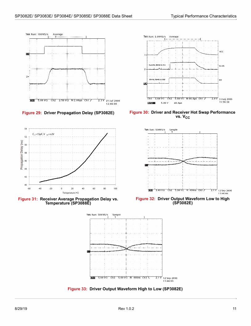
Figure 29: Driver Propagation Delay (SP3082E) Figure 30: Driver and Receiver Hot Swap Performance vs. VCC
Figure 31: Receiver Average Propagation Delay vs. Temperature (SP3088E)
Figure 32: Driver Output Waveform Low to High (SP3082E)
40
42
44
46
48
50
52
54
-60 -40 -20 0 20 40 60 80 100
Temperature (ºC)
C L=15pF, V ID =±2V
Prop
agat
ion
Del
ay (n
s)
Figure 33: Driver Output Waveform High to Low (SP3082E)
SP3082E/ SP3083E/ SP3084E/ SP3085E/ SP3088E Data Sheet Typical Performance Characteristics
8/29/19 Rev 1.0.2 12
Figure 34: Driver and Receiver Waveform High to Low (SP3082E)
Figure 35: Driver Propagation Delay (SP3083E - SP3085E)
Figure 36: Driver Output Waveform Low to High (SP3083E - SP3085E)
Figure 37: Driver Output Waveform High to Low (SP3083E - SP3085E)
Figure 38: Driver and Receiver Waveform Low to High (SP3082E)
Figure 39: Driver and Receiver Waveform Low to High (SP3083E - SP3085E)

SP3082E/ SP3083E/ SP3084E/ SP3085E/ SP3088E Data Sheet Typical Performance Characteristics
8/29/19 Rev 1.0.2 13
Figure 40: Driver Propagation Delay (SP3088E) Figure 41: Driver Output Waveform Low to High (SP3088E)
Figure 42: Driver Output Waveform High to Low (SP3088E)
Figure 43: Driver and Receiver Waveform Low to High (SP3088E)
Figure 44: Driver and Receiver Waveform High to Low (SP3083E - SP3085E)
Figure 45: Driver and Receiver Waveform High to Low (SP3088E)

SP3082E/ SP3083E/ SP3084E/ SP3085E/ SP3088E Data Sheet Typical Performance Characteristics
8/29/19 Rev 1.0.2 14
Figure 46: Receiver Propagation Delay (SP3088E) Figure 47: Receiver Propagation Delay (SP3082E)
-
Figure 48: Receiver Propagation Delay (SP3083E - SP3085E)

SP3082E/ SP3083E/ SP3084E/ SP3085E/ SP3088E Data Sheet Test Circuits and Timing Diagrams
8/29/19 Rev 1.0.2 15
Test Circuits and Timing Diagrams
Figure 49: Driver DC Test Circuit Figure 50: Receiver DC Test Circuit
Figure 51: Driver Propagation Delay Time Test Circuit and Timing Diagram
R/2
R/2 VO
D
VCC
VODDIOUT
R
A
BVID
RE
Y
Z
DDI
RL54
CL50pF
3.3V
VOD
t PHLt PLHZY
10%90%
10%90%
t SKEW = | t DPLH - t DPHL
V +O
VCC V CC /20DI
VV - V
DIFFV -O
1/2 V O
tR t F
VO
V CC /2
t DPLH t DPHL
|Y Z
0V

SP3082E/ SP3083E/ SP3084E/ SP3085E/ SP3088E Data Sheet Test Circuits and Timing Diagrams
8/29/19 Rev 1.0.2 16
Figure 52: Driver Short Circuit Current Limit Test Circuit
Figure 53: Driver Differential Output Test Circuit
Figure 54: Driver Enable and Disable Times Test Circuit and Timing Diagram
A / YDDI = 0 or VCC
B / Z
DE = 0 or VCC IOSD
100
-7V to +12V V
A / Y
B / Z
DDI = 0 or Vcc 60Ω
DE = 3.3V
VOD
375Ω
375Ω VCM
GENERATOR 50
S1
RL = 500
OUT
CL = 50pF
D0 or V CC
Z
YDI
DE
tLZ
0.25V
OUT
VCC
V OM = (V OL + V CC) / 2
tZL, tZL(SHDN)
VCC /20
0
SP3082E/ SP3083E/ SP3084E/ SP3085E/ SP3088E Data Sheet Test Circuits and Timing Diagrams
8/29/19 Rev 1.0.2 17
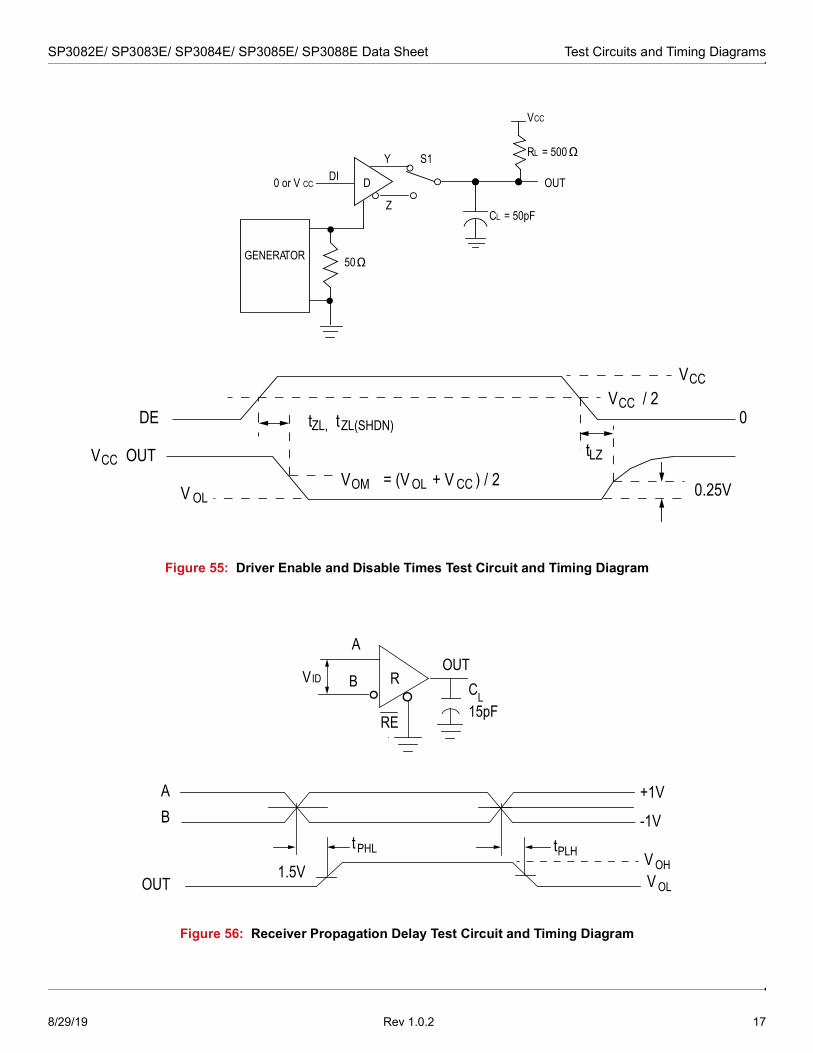
Figure 55: Driver Enable and Disable Times Test Circuit and Timing Diagram
Figure 56: Receiver Propagation Delay Test Circuit and Timing Diagram
GENERATOR 50
S1 RL = 500
OUT
CL = 50pF
D0 or V CC
Z
YDI
VCC
DE
V OL
tLZ
0.25V
VCC OUT
VCC
VOM = (V OL + V CC ) / 2
tZL, tZL(SHDN)
VCC / 20
OUTR
A
BVID
RE
CL15pF
t PHL tPLH
V OL1.5V
OUTV OH
AB
+1V
-1V

SP3082E/ SP3083E/ SP3084E/ SP3085E/ SP3088E Data Sheet Test Circuits and Timing Diagrams
8/29/19 Rev 1.0.2 18
Figure 57: Receiver Enable and Disable Times Test Circuit
Figure 58: Receiver Enable and Disable Timing Diagram
1.5V
-1.5V
S3
A
GENERATOR50
CL = 15pF
R1k
S1
S2
VCCB
RE
3V1.5V
RE
OUT
S1 is open S2 is closed S3 = 1.5V
V OH
tZH, t ZH(SHDN)
V OH /2
3V
0V1.5V
VCC
RE
OUT
S1 is closed, S2 is open, S3 = -1.5V
tZL, tZL(SHDN)
V OL = V CC /2VOL
3V1.5V
0V
RE
OUT
S1 is open S2 is closed S3 = 1.5V
V OH
tHZ
0.25V
3V
0V
1.5V
VCC
RE
OUT
S1 is closed, S2 is open, S3 = -1.5V
t LZ
VOL0.25V
SP3082E/ SP3083E/ SP3084E/ SP3085E/ SP3088E Data Sheet Test Circuits and Timing Diagrams
8/29/19 Rev 1.0.2 19
1. Test is performed to ensure survivability only. Normal operation during transient is not specified.
Figure 59: Transient Over Voltage Tolerance Test Circuit
100
Power-on or Power-off
C
A or Z
B or Y
Vtest+65.0Vand-65.0V15μs duration1% duty cycle
Generator,Receiver, orTransceiver

SP3082E/ SP3083E/ SP3084E/ SP3085E/ SP3088E Data Sheet Function Tables
8/29/19 Rev 1.0.2 20
Function TablesTable 9: SP3083E (Full Duplex)
TransmittingInputs Outputs
RE DE DI Y Z
X 1 1 1 0X 1 0 0 10 0 X High-Z1 0 X Shitdown
Table 10: SP3083E (Full Duplex)
ReceivingInputs Output
RE DE VA - VB RO
0 X ≥ -40mV 10 X ≤ -200mV 0
0 X Open, Shorted 1
1 1 X High-Z1 0 X Shutdown
Table 11: SP3084E (Full Duplex)
TransmittingInput Outputs
DI Y Z1 1 00 0 1
Open 1 0
Table 12: SP3084E (Full Duplex)
ReceivingInputs OutputVA - VB RO≥ -40mV 1≤ -200mV 0
Open / shorted 1
Note: Receiver inputs -200mV < VA - VB < -40mV should be considered indeterminate.
Table 13: SP3082E, SP3085E, SP3088E (Half Duplex)
TransmittingInputs Outputs
RE DE DI A B
X 1 1 1 0X 1 0 0 10 0 X High-Z1 0 X Shitdown
Table 14: SP3082E, SP3085E, SP3088E (Half Duplex)
ReceivingInputs Output
RE DE VA - VB RO
0 X ≥ -40mV 10 X ≤ -200mV 0
0 X Open / shorted 1
1 1 X High-Z1 0 X Shutdown

SP3082E/ SP3083E/ SP3084E/ SP3085E/ SP3088E Data Sheet Pin Information
8/29/19 Rev 1.0.2 21
Pin Information
Pin Configurations
Figure 60: Pin Configurations
Pin Descriptions
1. On 14-pin packages connect both pins 6 and 7 to Ground.
Table 15: Pin Descriptions
Pin NumberPin Name Pin FunctionFull Duplex Devices Half Duplex Devices
SP3083E SP3084E SP3082E, SP3085E, SP3088E
2 2 1 RO Receiver Output. When RE is low and if (A-B) ≥ -40mV, RO is High. If (A-B) ≤ -200mV, RO is low.
3 - 2 REReceiver Output Enable. When RE is low, RO is enabled. When RE is high, RO is high impedance. Drive RE high and DE low to enter shutdown mode. RE is a hot swap input.
4 - 3 DEDriver Output Enable. When DE is high, outputs are enabled. When DE is low, outputs are high impedance. Drive DE low and RE high to enter shutdown mode. DE is a hot-swap input.
5 3 4 DIDriver Input. With DE high, a low level on DI forces noninverting output low and inverting output high. A high level on DI forces noninverting output high and inverting output low.
6, 7 4 5 GND Ground9 5 - Y Noninverting Driver Output10 6 - Z Inverting Driver Output11 7 - B Inverting Receiver Input- - 7 B Inverting Receiver Input and Inverting Driver Output12 8 - A Noninverting Receiver Input- - 6 A Noninverting Receiver Input and Noninverting Driver Output
14 1 8 VCC Positive Supply VCC. Bypass to GND with a 0.1µF capacitor
1, 8, 13 - - NC No connect, not internally connected.
2
1
3
4 5
6
7
88 PIN NSOIC
Half Duplex
SP3082ESP3085ESP3088E
RO
RE
DE
DI GND
A
B
Vcc
2
1
3
4 5
6
7
88 PIN NSOIC
Full Duplex
SP3084E
Vcc
RO
DI
GND
A
B
Z
Y
2
1
3
4
5
6
7 8
9
10
11
12
13
14
14 PIN NSOIC
Full Duplex
SP3083EDI
NC
RO
RE
DE
GND
GND NC
Y
Z
B
A
NC
Vcc

SP3082E/ SP3083E/ SP3084E/ SP3085E/ SP3088E Data Sheet Detailed Description
8/29/19 Rev 1.0.2 22
Detailed DescriptionSP3082E - SP3088E are a family of advanced RS-485 /RS-422 transceivers. Each contains one driver and one receiver. These devices feature fail-safe circuitry that guarantees a logic-high receiver output when the receiver inputs are open or shorted, or when they are connected to a terminated transmission line with all drivers disabled. The SP3082E, SP3083E, SP3085E and SP3088E also feature a hot-swap capability allowing live insertion without error data transfer.
The SP3082E features reduced slew-rate drivers that minimize EMI and reduce reflections caused by improperly terminated cables, allowing error-free data transmission up to 115kbps. The SP3083E, SP3084E and SP3085E also offer slew-rate limits allowing transmit speeds up to 500kbps. The SP3088E driver slew rate is not limited, making transmit speeds up to 20Mbps possible.
The SP3082E, SP3085E and SP3088E are half-duplextransceivers, while the SP3083E and SP3084E are fullduplex transceivers.All devices operate from a single 5.0V supply. Drivers are output short-circuit current limited. Thermal-shutdown circuitry protects drivers against excessive power dissipation. When activated, the thermal-shutdown circuitry places the driver outputs into a high-impedance state.
Receiver Input FilteringSP3082E-SP3085E receivers incorporate input filtering in addition to input hysteresis. This filtering enhances noise immunity with differential signals that have very slow rise and fall times. Receiver propagation delay increases due to this filtering.
Advanced Fail SafeOrdinary RS-485 differential receivers will be in an indeterminate state whenever A - B is less than ±200mV. This situation can occur whenever the data bus is not being actively driven. The Advanced Failsafe feature of the SP308xE family guarantees a logic-high receiver output if the receiver’s differential inputs are shorted, open-circuit or if they are shunted by a termination resistor.
The receiver thresholds of the SP308xE family are very precise and offset by at least a 40mV noise margin from ground. This results in a logic-high receiver output at zero volts input differential while maintaining compliance with the EIA / TIA-485 standard of ±200mV.
Hot-Swap CapabilityWhen a microprocessor or other logic device undergoes its power-up sequence, its logic-outputs are typically at high impedance. In this state they are unable to drive the DE and signals to a defined logic level. During this period, noise, parasitic coupling or leakage from other devices could cause standard CMOS enable inputs to drift to an incorrect logic level.
If circuit boards are inserted into an energized backplane (commonly called "live insertion’ or ’hot swap’), power may be suddenly applied to all circuits. Without the hot-swap capability, this situation could improperly enable the transceiver’s driver or receiver, driving invalid data onto shared busses and possibly causing driver contention or device damage.
The SP308x family contains a special power-on-reset circuit that holds DE low and RE high for approximately 10 microseconds. After this initial power-up sequence, the hot-swap circuit becomes transparent, allowing for normal, unskewed enable and disable timings.
±15kV ESD ProtectionESD-protection structures are incorporated on all pins to protect against electrostatic discharges encountered during handling and assembly. The driver output and receiver inputs of the SP308xE family have extra protection against static electricity. MaxLinear's uses state of the art structures to protect these pins against ESD of ±15kV without damage. The ESD structures withstand high ESD in all states: normal operation, shutdown and powered down. After an ESD event, the SP3082E - SP3088E keep working without latchup or damage.
ESD protection can be tested in various ways. The transmitter outputs and receiver inputs of the SP3082E - SP3088E are characterized for protection to the following limits:
±15kV using the Human Body Model
±8kV using the Contact Discharge method specified in IEC 61000-4-2
±15kV Air-gap

SP3082E/ SP3083E/ SP3084E/ SP3085E/ SP3088E Data Sheet Detailed Description
8/29/19 Rev 1.0.2 23
ESD Test ConditionsESD performance depends on a variety of conditions. Contact MaxLinear for a reliability report that documents test setup, methodology and results.
IEC 61000-4-2The IEC 61000-4-2 standard covers ESD testing and performance of finished equipment. However, it does not specifically refer to integrated circuits. The SP308xE family helps you design equipment to meet IEC 61000-4-2, without sacrificing board space and cost for external ESD-protection components.
The major difference between tests done using the Human Body Model and IEC 61000-4-2 is higher peak current in IEC 61000-4-2, as series resistance is lower in the IEC 61000-4-2 model. Hence, the ESD withstand voltage measured to IEC 61000-4-2 is generally lower than that measured using the Human Body Model. The air-gap test involves approaching the device with a charged probe. The contact-discharge method connects the probe to the device before the probe is energized.
Machine ModelThe machine model for ESD tests all pins using a 200pF storage capacitor and zero discharge resistance. The objective is to emulate the stress caused when I/O pins are contacted by handling equipment during test and assembly.
256 Transceivers on the BusThe standard RS-485 receiver input impedance is 12kΩ (1 unit load). A standard driver can drive up to 32 unit loads. The SP308xE family of transceivers has only a 1/8-unit load receiver input impedance (96kΩ), thereby allowing eight times as many,up to 256, transceivers to be connected in parallel on a communication line. Any combination of these devices and other RS-485 transceivers up to a total of 32 unit loads may be connected to the line.
Low Power Shutdown ModeLow-power shutdown mode is initiated by bringing both RE high and DE low simultaneously. While in shutdown, devices typically draw only 50nA of supply current. DE and RE may be tied together and driven by a single control signal. Devices are guaranteed not to enter shutdown if RE is high and DE is low for less than 50ns. If the inputs are in this state for at least 600ns, the parts are shutdown.
Enable times tZH and tZL apply when the part was not in a low-power shutdown state. Enable times tZH(SHDN) and tZL(SHDN) apply when the parts are shut down. It drivers and receivers take longer to become enabled from low-power shutdown mode tZH(SHDN) and tZL(SHDN) than from driver /receiver-disable mode (tZH, tZL).
Driver Output ProtectionTwo mechanisms prevent excessive output current and power dissipation caused by faults or by bus contention. First, a driver current limit on the output stage provides immediate protection against short circuits over the whole common-mode voltage range. Second, a thermal-shutdown circuit forces the driver outputs into a high-impedance state if junction temperature becomes excessive.
Line Length, EMI and ReflectionsSP3082E - SP3085E feature controlled slew-rate drivers that minimize EMI and reduce reflections caused by improperly terminated cables.
SP3082E driver rise and fall times are limited to no faster than 667ns, allowing error-free data transmission up to 115kbps. The SP3083E, SP3084E and SP3085E offer somewhat higher driver output slew-rate limits, allowing transmit speeds up to 500kbps.
The RS-485 / RS422 standard covers line lengths up to 4,000ft. Maximum achievable line length is a function of signal attenuation and noise. Use of slew-controlled drivers such as the SP3082E - SP3085E may help to reduce crosstalk interference and permit communication over longer transmission lines.
Termination prevents reflections by eliminating the impedance mismatches on a transmission line. Line termination is typically used if rise and fall times are shorter than the round-trip signal propagation time. Slew-limited drivers may reduce or eliminate the need for cable termination in many applications.

SP3082E/ SP3083E/ SP3084E/ SP3085E/ SP3088E Data Sheet Detailed Description
8/29/19 Rev 1.0.2 24
Typical Applications
Figure 61: Half-Duplex Network
Figure 62: Bi-Directional Full-Duplex Network
Figure 63: Point to Multi-Point Repeater
Repeater(optional)

SP3082E/ SP3083E/ SP3084E/ SP3085E/ SP3088E Data Sheet Mechanical Dimensions
8/29/19 Rev 1.0.2 25
Mechanical Dimensions
NSOIC8
Figure 64: Mechanical Dimension, NSOIC8
Drawing No:
Revision: A
Side View Front View
POD-00000108

SP3082E/ SP3083E/ SP3084E/ SP3085E/ SP3088E Data Sheet Mechanical Dimensions
8/29/19 Rev 1.0.2 26
Mechanical Dimensions
NSOIC14
Figure 65: Mechanical Dimensions, NSOIC14
Drawing No:
Revision: A
Side View
Top View
Front View
POD-00000109

SP3082E/ SP3083E/ SP3084E/ SP3085E/ SP3088E Data Sheet Ordering Information
8/29/19 Rev 1.0.2 27
Ordering Information
1. Refer to www.maxlinear.com/SP3082E, www.maxlinear.com/SP3083E, www.maxlinear.com/SP3084E, www.maxlinear.com/SP3085E, and www.maxlinear.com/SP3088E for most up-to-date Ordering Information.
2. Visit www.maxlinear.com for additional information on Environmental Rating.
Table 16: Ordering Information(1)
Ordering Part Number Operating Temperature Range Package Packaging Method Lead-Free(2)
SP3082EEN-L -40°C to 85°C NSOIC8 Tube YesSP3082EEN-L/TR -40°C to 85°C NSOIC8 Reel YesSP3083EEN-L/TR -40°C to 85°C NSOIC14 Reel YesSP3084EEN-L/TR -40°C to 85°C NSOIC8 Reel YesSP3085EEN-L -40°C to 85°C NSOIC8 Tube YesSP3085EEN-L/TR -40°C to 85°C NSOIC8 Reel YesSP3088EEN-L -40°C to 85°C NSOIC8 Tube YesSP3088EEN-L/TR -40°C to 85°C NSOIC8 Reel Yes

The content of this document is furnished for informational use only, is subject to change without notice, and should not be construed as a commitment byMaxLinear, Inc. MaxLinear, Inc. assumes no responsibility or liability for any errors or inaccuracies that may appear in the informational content contained in thisguide. Complying with all applicable copyright laws is the responsibility of the user. Without limiting the rights under copyright, no part of this document may bereproduced into, stored in, or introduced into a retrieval system, or transmitted in any form or by any means (electronic, mechanical, photocopying, recording, orotherwise), or for any purpose, without the express written permission of MaxLinear, Inc.
Maxlinear, Inc. does not recommend the use of any of its products in life support applications where the failure or malfunction of the product can reasonably beexpected to cause failure of the life support system or to significantly affect its safety or effectiveness. Products are not authorized for use in such applications unlessMaxLinear, Inc. receives, in writing, assurances to its satisfaction that: (a) the risk of injury or damage has been minimized; (b) the user assumes all such risks; (c)potential liability of MaxLinear, Inc. is adequately protected under the circumstances.
MaxLinear, Inc. may have patents, patent applications, trademarks, copyrights, or other intellectual property rights covering subject matter in this document. Exceptas expressly provided in any written license agreement from MaxLinear, Inc., the furnishing of this document does not give you any license to these patents,trademarks, copyrights, or other intellectual property.
MaxLinear, the MaxLinear logo, and any MaxLinear trademarks, MxL, Full-Spectrum Capture, FSC, G.now, AirPHY and the MaxLinear logo are all on the productssold, are all trademarks of MaxLinear, Inc. or one of MaxLinear’s subsidiaries in the U.S.A. and other countries. All rights reserved. Other company trademarks andproduct names appearing herein are the property of their respective owners.
© 2007 - 2019 MaxLinear, Inc. All rights reserved.
SP3082E/ SP3083E/ SP3084E/ SP3085E/ SP3088E Data Sheet Disclaimer
MaxLinear, Inc.5966 La Place Court, Suite 100Carlsbad, CA 92008760.692.0711 p.760.444.8598 f.
www.maxlinear.com