
Solid State Relays Overview and Applications OCMOS FET using a photo Detector to drive the MOS FET...
29
CONTENTS 1. INTRODUCTION....................................................................................................................................................... 2 2. FEATURES, STRUCTURES, COMPOSITION AND THEORY OF OPERATION .................................................... 3 2.1 FEATURES ...................................................................................................................................................... 3 2.2 STRUCTURES................................................................................................................................................. 3 2.3 COMPOSITION................................................................................................................................................ 6 2.4 THEORY OF OPERATION .............................................................................................................................. 6 3. MAINLY CHARACTERISTICS ................................................................................................................................. 7 3.1 OFFSET VOLTAGE ......................................................................................................................................... 7 3.2 TEMPERATURE CHARACTERISTICS ........................................................................................................... 8 4. CHARACTERISTICS VALUES AND MEASURING CHARACTERISTIC VALUES ............................................... 15 4.1 CHARACTERISTICS VALUES ...................................................................................................................... 15 4.2 MEASURING CHARACTERISTIC VALUES .................................................................................................. 16 5. APPLICATIONS...................................................................................................................................................... 19 5.1 COMMUNICATION LINES ............................................................................................................................. 19 5.2 INPUT/OUTPUT INTERFACE ....................................................................................................................... 22 5.3 LOW-LEVEL/ANALOG SIGNAL CONTROL .................................................................................................. 24 6. COMPARISION WITH OTHER SWITCHING DEVICES ......................................................................................... 25 7. CAUTIONS FOR USE............................................................................................................................................. 26 8. CONCLUSION ........................................................................................................................................................ 29 Solid State Relays Overview And Applications AN3000 California Eastern Laboratories A PPLICATION N OTE
Transcript of Solid State Relays Overview and Applications OCMOS FET using a photo Detector to drive the MOS FET...
CONTENTS
1. INTRODUCTION....................................................................................................................................................... 2
2. FEATURES, STRUCTURES, COMPOSITION AND THEORY OF OPERATION .................................................... 3
2.1 FEATURES ...................................................................................................................................................... 3
2.2 STRUCTURES................................................................................................................................................. 3
2.3 COMPOSITION................................................................................................................................................ 6
2.4 THEORY OF OPERATION .............................................................................................................................. 6
3. MAINLY CHARACTERISTICS ....................................................................................................... .......................... 7
3.1 OFFSET VOLTAGE ......................................................................................................................................... 7
3.2 TEMPERATURE CHARACTERISTICS ........................................................................................................... 8
4. CHARACTERISTICS VALUES AND MEASURING CHARACTERISTIC VALUES............................................... 15
4.1 CHARACTERISTICS VALUES ...................................................................................................................... 15
4.2 MEASURING CHARACTERISTIC VALUES ............................................................................................. ..... 16
5. APPLICATIONS...................................................................................................................................................... 19
5.1 COMMUNICATION LINES............................................................................................................................. 19
5.2 INPUT/OUTPUT INTERFACE ....................................................................................................................... 22
5.3 LOW-LEVEL/ANALOG SIGNAL CONTROL .................................................................................................. 24
6. COMPARISION WITH OTHER SWITCHING DEVICES......................................................................................... 25
7. CAUTIONS FOR USE............................................................................................................................................. 26
8. CONCLUSION ........................................................................................................................................................ 29
Solid State Relays Overview And ApplicationsAN3000
California Eastern Laboratories A P P L I C A T I O N N O T E

2
1. INTRODUCTIION
The SSR that NEC has started marketing uses a photocoupler system with a MOS FET, explained in the following,
as an output switch and a combination of an Emitter and Photo Detector to drive the switch.
NEC’s SSR is named a “OCMOS FET (Opto-Coupled MOS FET)” as the input and output are isolated with a
photocoupler and the MOS FET switch is used as an output switch.
The OCMOS FET using a photo Detector to drive the MOS FET is a new type of SSR developed recently and
being commercialized.
An OCMOS FET operates this way: A control signal applied to the OCMOS FET input terminals triggers the output
switch of the OCMOS FET, which, in turn, opens or closes the output terminals.
A normally-off type (which is functionally the same as a “make contact” mechanical relay) leaves the output
terminals open, if there is no input signal, and short-circuits the output terminals if an input signal above the threshold
level is applied. Conversely, a normally-on type (which is functionally the same as a “break contact” mechanical
relay) keeps the output terminals short-circuited, if there is no input signal, and opens the output terminals by an
input signal.
AN3000
3
2. FEATURES, STRUCTURES, COMPOSITION AND THEORY OF OPERATION
2.1 FEATURES
The general features of OCMOS FET as follows:
1) High sensitivity and low driving power. Can be driven directly by a TTL or CMOS.
2) Can switch low to high-voltage level signals or an AC/DC load current at a low power level.
3) Extremely low offset voltage (in the on-state) and very small leakage current (in the off-state). Applicable even
to low-level signals.
4) dv/dt insensitive, No possibility of malfunction caused by noise signals due to abrupt startup. No thermal
runaway, as seen bipolar elements.
5) Use of bidirectional MOS FET support DC and AC switching.
6) A compact DIP/SOP package which can be mounted like other electronic components.
2.2 STRUCTURES
Compared with a mechanical relay, the input and output control sections, made up of the LED and PVD in the
OCMOS FET, correspond to the coil in the mechanical relay. They isolate the input from output and generate an
output control signal on receipt of an input signal.
The MOS FET in the OCMOS FET corresponds to the contact in the mechanical relay, opening and closing the
load circuit.
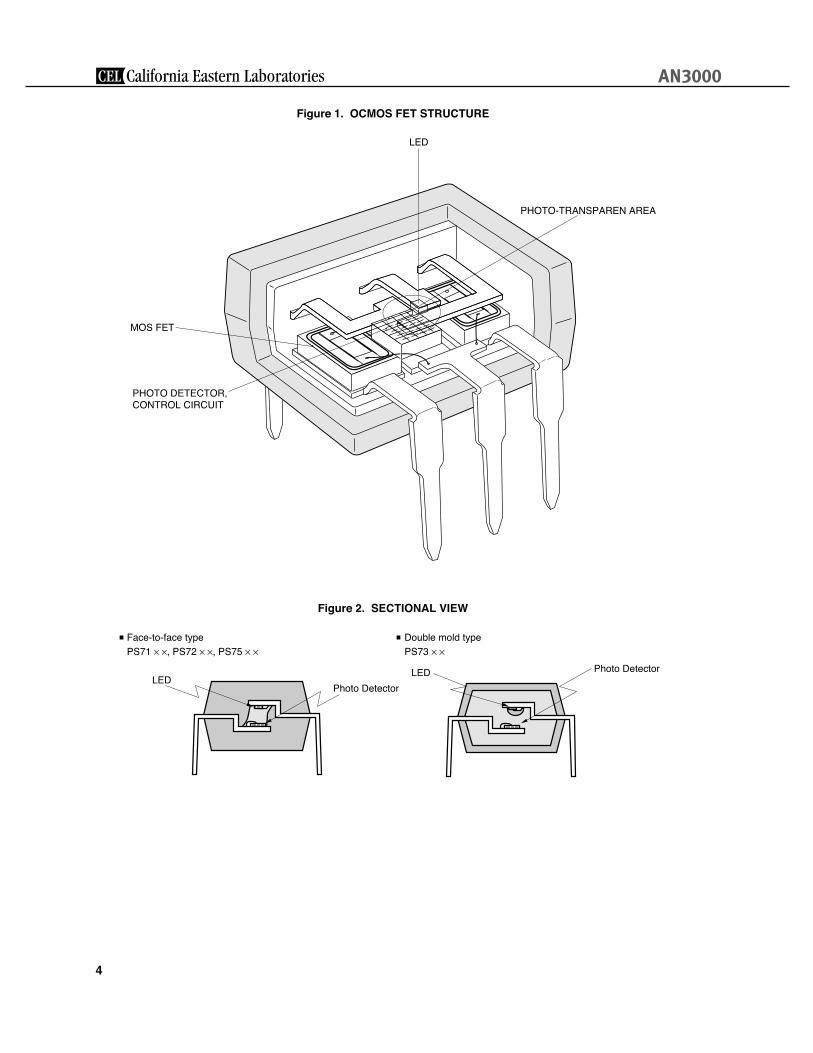
Figure 1 shows the OCMOS FET structure. Figure 2 shows the sectional view. The semiconductor chip, a
subcomponent of the OCMOS FET is mounted at a required position on the metal support, called a lead frame, also
serving as a terminal, using conducting paste. (The procedure is called chip mounting.)
Next, the chip electrodes are connected to a fine gold wire to the lead, which becomes a terminal. (The procedure
is called wire bonding.) Then as regards face-to-face type, the LED and PVD are covered with transparent silicone
rubber to form an optical path. This is put into a furnace for hardening and then molded with epoxy resin.
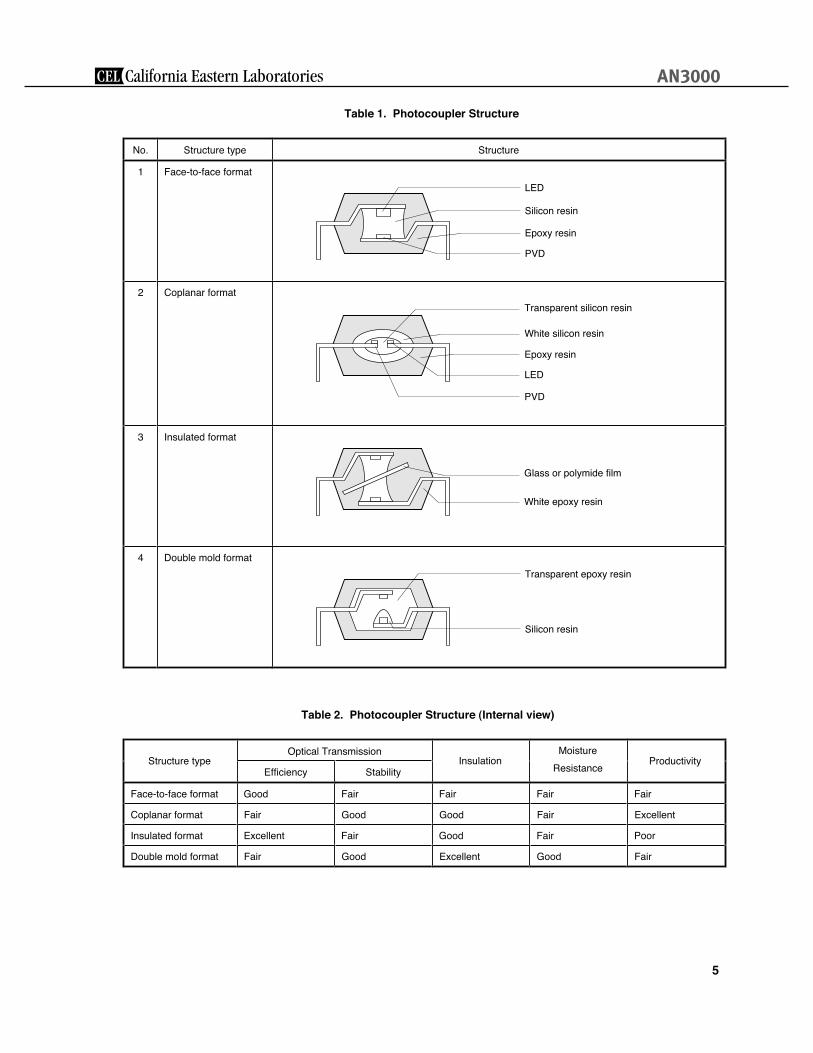
There is more than one kind of structure that links LED and PVD (called a photocoupler structure). Table 1 shows
an example of the structure type and Table 2 compares the different structures. (NEC’s OCMOS FET series are
face-to-face type and double mold type.)
AN3000
4
Figure 1. OCMOS FET STRUCTURE
LED
PHOTO-TRANSPAREN AREA
MOS FET
PHOTO DETECTOR,CONTROL CIRCUIT
Figure 2. SECTIONAL VIEW
Photo DetectorLED
PS71 , PS72 , PS75 PS73epytdlomelbuoDepytecaf-ot-ecaF
Photo DetectorLED
AN3000
5
Table 1. Photocoupler Structure
erutcurtSepyterutcurtS.oN
1 Face-to-face format
LED
Silicon resin
Epoxy resin
PVD
2 Coplanar format
Transparent silicon resin
White silicon resin
Epoxy resin
LED
PVD
3 Insulated format
Glass or polymide film
White epoxy resin
4 Double mold format
Transparent epoxy resin
Silicon resin
Table 2. Photocoupler Structure (Internal view)
Optical Transmission
Efficiency Stability
Face-to-face format Good Fair Fair Fair Fair
Coplanar format Fair Good Good Fair Excellent
Insulated format Excellent Fair Good Fair Poor
Double mold format Fair Good Excellent Good Fair
Moisture
ResistanceProductivityInsulationStructure type
AN3000

6
2.3 COMPOSITION
As shown in Figure 3, the NEC OCMOS FET consists of an Emitter, Photo Detector, Control Circuit, and the MOS
FET.
Figure 3. OCMOS FET COMPOSITION
Input Output
Lightsignal
Em
itter
Pho
to D
etec
tor
Con
trol
Circ
uit
MOS FET
)edoiDciatloVotohP(DVP:rotceteDotohPDEL:rettimE
2.4 THEORY OF OPERATION
Normally-off type. Theory of operation as follows.
When an input signal current flows across the input terminals, the LED emits light. Some of the light is shot
directly into the PVD via the transparent silicon layer, while the rest of the light reaches the PVD after being reflected
from the transparent silicon boundary surface. On receiving the light, the PVD generates a current corresponding to
the amount of incident radiation received.
The current passes through the control section to charge the MOS FET gate capacity, raising the gate voltage.
When the gate voltage reaches a certain voltage value, current flows between the MOS FET drain and source. Since
the drain and source are connected to the output terminals, the external load circuit across the output terminals is
closed.
When the input signal current is disconnected, the LED stops emission and the PVD voltage drops. In this
condition, the charges stored in the MOS FET gate are not released quickly, instead the FET remains conductive. If
the control circuit is operated to cause the MOS FET gate charges to be released quickly, the MOS FET gate voltage
will be dropped. If the voltage drops to a certain level, the MOS FET drain and source will be isolated again.
AN3000

7
3. MAINLY CHARACTERISTICS
3.1 OFFSET VOLTAGE
Figure 4 shows LOAD CURRENT (IL)-LOAD VOLTAGE (VL) characteristic for the MOS FET. When VL is low, the
current changes, as in a DC in a DC resistor. That is, there is no offset voltage.
Figure 4. Comparing OCMOS FET with a Photocoupler and Thyristor
(a) OCMOS FET
Load Voltage VL (V)
Load
Cur
rent
IL (
mA
)
(b) Photocoupler
Load Voltage VL (V)Lo
ad C
urre
nt IL
(m
A)
(c) Thyristor
Load Voltage VL (V)
Load
Cur
rent
IL (
mA
)
AN3000
8
3.2 TEMPERATURE CHARACTERISTICS
3.2.1 TURN-ON TIME CHARACTERISTICS
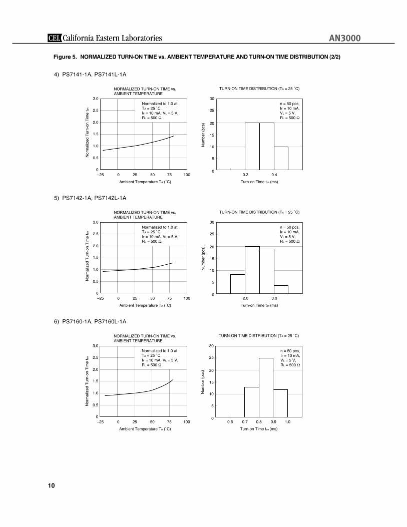
Figure 5 shows the NORMALIZED TURN-ON TIME vs. AMBIENT TEMPERATURE and the TURN-ON TIME
DISTRIBUTION of a normally-off type OCMOS FET. (Such as the PS7112, PS7113, PS7122, PS7141, PS7142 and
PS7160 OCMOS FET.)
3.2.2 TURN-OFF TIME CHARACTERISTICS
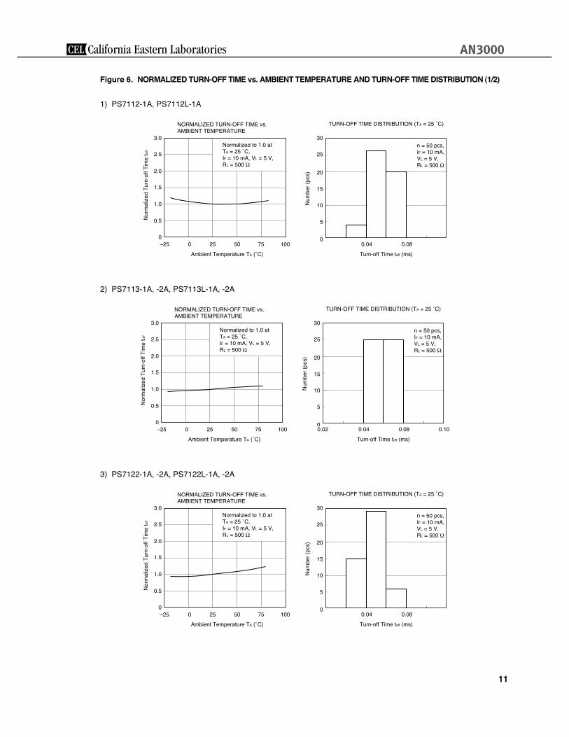
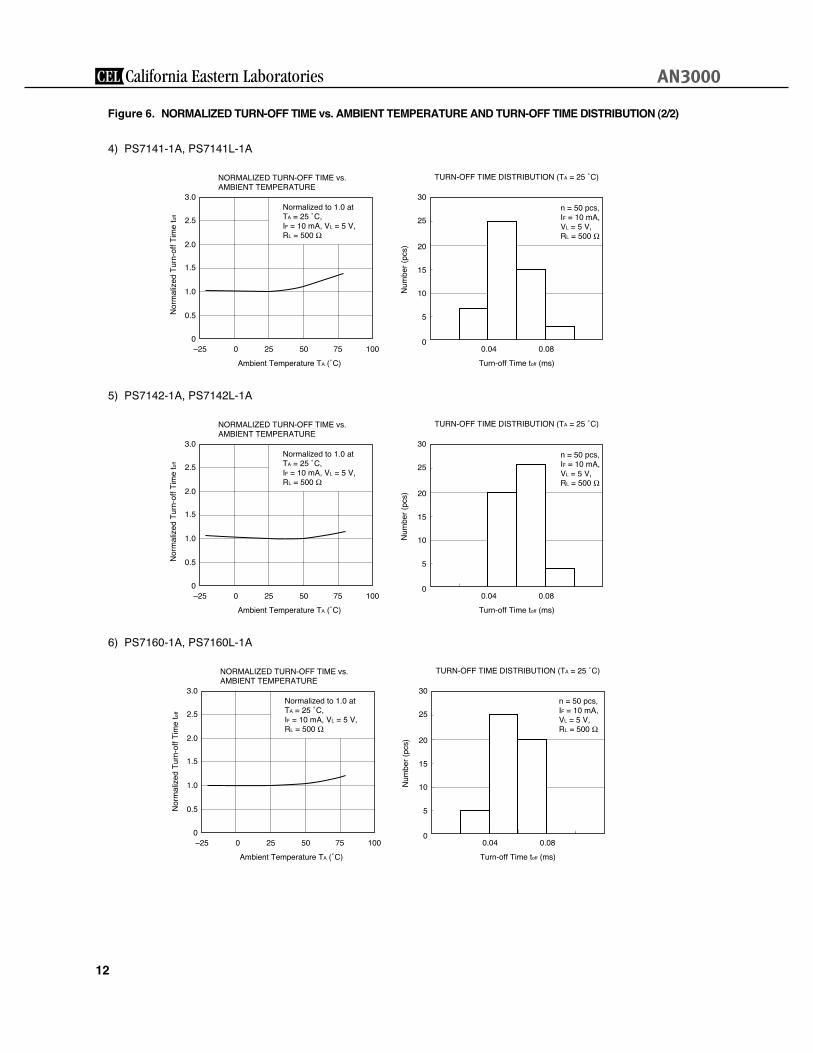
Figure 6 shows the NORMALIZED TURN-OFF TIME vs. AMBIENT TEMPERATURE and the TURN-OFF TIME
DISTRIBUTION of a normally-off type OCMOS FET. (Such as the PS7112, PS7113, PS7122, PS7141, PS7142 and
PS7160 OCMOS FET.)
3.2.3 ON-STATE RESISTANCE CHARACTERISTICS
Figure 7 shows the NORMALIZED ON-STATE RESISTANCE vs. AMBIENT TEMPERATURE and the ON-STATE
RESISTANCE DISTRIBUTION of a normally-off type OCMOS FET. (Such as the PS7112, PS7113, PS7122,
PS7141, PS7142 and PS7160 OCMOS FET.)
AN3000

9
Figure 5. NORMALIZED TURN-ON TIME vs. AMBIENT TEMPERATURE AND TURN-ON TIME DISTRIBUTION (1/2)
1) PS7112-1A, PS7112L-1A
1000–25
2.5
3.0
Nor
mal
ized
Tur
n-on
Tim
e to
n
Ambient Temperature TA ( C)
NORMALIZED TURN-ON TIME vs. AMBIENT TEMPERATURE
025 50 75
2.0
1.5
1.0
0.5
Normalized to 1.0 atTA = 25 C,IF = 10 mA, VL = 5 V,RL = 500
Num
ber
(pcs
)
Turn-on Time ton (ms)
0
5
10
15
20
25
30n = 50 pcs,IF = 10 mA,VL = 5 V,RL = 500
TURN-ON TIME DISTRIBUTION (TA = 25 C)
0.1 0.2 0.3
2) PS7113-1A, -2A, PS7113L-1A, -2A
1000–25
2.5
3.0
Nor
mal
ized
Tur
n-on
Tim
e to
n
Ambient Temperature TA ( C)
NORMALIZED TURN-ON TIME vs. AMBIENT TEMPERATURE
025 50 75
2.0
1.5
1.0
0.5
Normalized to 1.0 atTA = 25 C,IF = 10 mA, VL = 5 V,RL = 500
Num
ber
(pcs
)
Turn-on Time ton (ms)
0
5
10
15
20
25
30n = 50 pcs,IF = 10 mA,VL = 5 V,RL = 500
TURN-ON TIME DISTRIBUTION (TA = 25 C)
1.1 1.21.0 1.3 1.4 1.5 1.6
3) PS7122-1A, -2A, PS7122L-1A, -2A
1000–25
2.5
3.0
Nor
mal
ized
Tur
n-on
Tim
e to
n
Ambient Temperature TA ( C)
NORMALIZED TURN-ON TIME vs. AMBIENT TEMPERATURE
025 50 75
2.0
1.5
1.0
0.5
Normalized to 1.0 atTA = 25 C,IF = 10 mA, VL = 5 V,RL = 500
Num
ber
(pcs
)
Turn-on Time ton (ms)
0
5
10
15
20
25
30n = 50 pcs,IF = 10 mA,VL = 5 V,RL = 500
TURN-ON TIME DISTRIBUTION (TA = 25 C)
0.4 0.6 0.80.5 0.7
AN3000
10
Figure 5. NORMALIZED TURN-ON TIME vs. AMBIENT TEMPERATURE AND TURN-ON TIME DISTRIBUTION (2/2)
4) PS7141-1A, PS7141L-1A
1000–25
2.5
3.0
Nor
mal
ized
Tur
n-on
Tim
e to
n
Ambient Temperature TA ( C)
NORMALIZED TURN-ON TIME vs. AMBIENT TEMPERATURE
025 50 75
2.0
1.5
1.0
0.5
Normalized to 1.0 atTA = 25 C,IF = 10 mA, VL = 5 V,RL = 500
Num
ber
(pcs
)
Turn-on Time ton (ms)
0
5
10
15
20
25
30n = 50 pcs,IF = 10 mA,VL = 5 V,RL = 500
TURN-ON TIME DISTRIBUTION (TA = 25 C)
0.3 0.4
5) PS7142-1A, PS7142L-1A
1000–25
2.5
3.0
Nor
mal
ized
Tur
n-on
Tim
e t o
n
Ambient Temperature TA ( C)
NORMALIZED TURN-ON TIME vs. AMBIENT TEMPERATURE
025 50 75
2.0
1.5
1.0
0.5
Normalized to 1.0 atTA = 25 C,IF = 10 mA, VL = 5 V,RL = 500
Num
ber
(pcs
)
Turn-on Time ton (ms)
0
5
10
15
20
25
30n = 50 pcs,IF = 10 mA,VL = 5 V,RL = 500
TURN-ON TIME DISTRIBUTION (TA = 25 C)
2.0 3.0
6) PS7160-1A, PS7160L-1A
n = 50 pcs,IF = 10 mA,VL = 5 V,RL = 500
1000–25
2.5
3.0
Nor
mal
ized
Tur
n-on
Tim
e to
n
Ambient Temperature TA ( C)
NORMALIZED TURN-ON TIME vs. AMBIENT TEMPERATURE
025 50 75
2.0
1.5
1.0
0.5
Normalized to 1.0 atTA = 25 C,IF = 10 mA, VL = 5 V,RL = 500
Num
ber
(pcs
)
Turn-on Time ton (ms)
0
5
10
15
20
25
30
TURN-ON TIME DISTRIBUTION (TA = 25 C)
0.6 0.8 1.00.7 0.9
AN3000
11
Figure 6. NORMALIZED TURN-OFF TIME vs. AMBIENT TEMPERATURE AND TURN-OFF TIME DISTRIBUTION (1/2)
1) PS7112-1A, PS7112L-1A
n = 50 pcs,IF = 10 mA,VL = 5 V,RL = 500
1000–25
2.5
3.0N
orm
aliz
ed T
urn-
off T
ime
toff
Ambient Temperature TA ( C)
NORMALIZED TURN-OFF TIME vs. AMBIENT TEMPERATURE
025 50 75
2.0
1.5
1.0
0.5
Normalized to 1.0 atTA = 25 C,IF = 10 mA, VL = 5 V,RL = 500
Num
ber
(pcs
)
Turn-off Time toff (ms)
0
5
10
15
20
25
30
TURN-OFF TIME DISTRIBUTION (TA = 25 C)
0.04 0.08
2) PS7113-1A, -2A, PS7113L-1A, -2A
n = 50 pcs,IF = 10 mA,VL = 5 V,RL = 500
1000–25
2.5
3.0
Nor
mal
ized
Tur
n-of
f Tim
e to
ff
Ambient Temperature TA ( C)
NORMALIZED TURN-OFF TIME vs. AMBIENT TEMPERATURE
025 50 75
2.0
1.5
1.0
0.5
Normalized to 1.0 atTA = 25 C,IF = 10 mA, VL = 5 V,RL = 500
Num
ber
(pcs
)
Turn-off Time toff (ms)
0
5
10
15
20
25
30
TURN-OFF TIME DISTRIBUTION (TA = 25 C)
0.04 01.020.0 0.08
3) PS7122-1A, -2A, PS7122L-1A, -2A
n = 50 pcs,IF = 10 mA,VL = 5 V,RL = 500
1000–25
2.5
3.0
Nor
mal
ized
Tur
n-of
f Tim
e to
ff
Ambient Temperature TA ( C)
NORMALIZED TURN-OFF TIME vs. AMBIENT TEMPERATURE
025 50 75
2.0
1.5
1.0
0.5
Normalized to 1.0 atTA = 25 C,IF = 10 mA, VL = 5 V,RL = 500
Num
ber
(pcs
)
Turn-off Time toff (ms)
0
5
10
15
20
25
30
TURN-OFF TIME DISTRIBUTION (TA = 25 C)
0.04 0.08
AN3000
12
Figure 6. NORMALIZED TURN-OFF TIME vs. AMBIENT TEMPERATURE AND TURN-OFF TIME DISTRIBUTION (2/2)
4) PS7141-1A, PS7141L-1A
n = 50 pcs,IF = 10 mA,VL = 5 V,RL = 500
1000–25
2.5
3.0
Nor
mal
ized
Tur
n-of
f Tim
e to
ff
Ambient Temperature TA ( C)
NORMALIZED TURN-OFF TIME vs. AMBIENT TEMPERATURE
025 50 75
2.0
1.5
1.0
0.5
Normalized to 1.0 atTA = 25 C,IF = 10 mA, VL = 5 V,RL = 500
Num
ber
(pcs
)
Turn-off Time toff (ms)
0
5
10
15
20
25
30
TURN-OFF TIME DISTRIBUTION (TA = 25 C)
0.04 0.08
5) PS7142-1A, PS7142L-1A
n = 50 pcs,IF = 10 mA,VL = 5 V,RL = 500
1000–25
2.5
3.0
Nor
mal
ized
Tur
n-of
f Tim
e to
ff
Ambient Temperature TA ( C)
NORMALIZED TURN-OFF TIME vs. AMBIENT TEMPERATURE
025 50 75
2.0
1.5
1.0
0.5
Normalized to 1.0 atTA = 25 C,IF = 10 mA, VL = 5 V,RL = 500
Num
ber
(pcs
)
Turn-off Time toff (ms)
0
5
10
15
20
25
30
TURN-OFF TIME DISTRIBUTION (TA = 25 C)
0.04 0.08
6) PS7160-1A, PS7160L-1A
Normalized to 1.0 atTA = 25 C,IF = 10 mA, VL = 5 V,RL = 500
1000–25
2.5
3.0
Nor
mal
ized
Tur
n-of
f Tim
e to
ff
Ambient Temperature TA ( C)
NORMALIZED TURN-OFF TIME vs. AMBIENT TEMPERATURE
025 50 75
2.0
1.5
1.0
0.5
Num
ber
(pcs
)
Turn-off Time toff (ms)
0
5
10
15
20
25
30
TURN-OFF TIME DISTRIBUTION (TA = 25 C)
0.04 0.08
n = 50 pcs,IF = 10 mA,VL = 5 V,RL = 500
AN3000
13
Figure 7. NORMALIZED ON-STATE RESISTANCE vs. AMBIENT TEMPERATURE AND TURN-ON TIME DISTRIBUTION
(1/2)
1) PS7112-1A, PS7112L-1A
On-State Resistance Ron ( )
Num
ber
(pcs
)
0
5
10
15
20
25
30n = 50 pcs,IF = 5 mA,IL = 1 mA
ON-STATE RESISTANCE DISTRIBUTION (TA = 25 C)
2.8 2.9 3.01000–25
2.5
3.0
Nor
mal
ized
On-
Sta
te R
esis
tanc
e R
on
Ambient Temperature TA ( C)
NORMALIZED ON-STATE RESISTANCE vs. AMBIENT TEMPERATURE
025 50 75
2.0
1.5
1.0
0.5
Normalized to 1.0 atTA = 25 C,IF = 5 mA, IL = 1 mA
2) PS7113-1A, -2A, PS7113L-1A, -2A
On-State Resistance Ron ( )
Num
ber
(pcs
)
0
5
10
15
20
25
30n = 50 pcs,IF = 5 mA,IL = 1 mA
ON-STATE RESISTANCE DISTRIBUTION (TA = 25 C)
0.8 0.9 1.01000–25
2.5
3.0
Nor
mal
ized
On-
Sta
te R
esis
tanc
e R
on
Ambient Temperature ( C)
NORMALIZED ON-STATE RESISTANCE vs. AMBIENT TEMPERATURE
025 50 75
2.0
1.5
1.0
0.5
Normalized to 1.0 atTA = 25 C,IF = 5 mA, IL = 1 mA
3) PS7122-1A, 2A, PS7122L-1A, -2A
On-State Resistance Ron ( )
Num
ber
(pcs
)
0
5
10
15
20
25
30n = 50 pcs,IF = 5 mA,IL = 1 mA
ON-STATE RESISTANCE DISTRIBUTION (TA = 25 C)
2.8 3.0 3.22.9 3.11000–25
2.5
3.0
Nor
mal
ized
On-
Sta
te R
esis
tanc
e R
on
Ambient Temperature TA ( C)
NORMALIZED ON-STATE RESISTANCE vs. AMBIENT TEMPERATURE
025 50 75
2.0
1.5
1.0
0.5
Normalized to 1.0 atTA = 25 C,IF = 5 mA, IL = 1 mA
AN3000

14
Figure 7. NORMALIZED ON-STATE RESISTANCE vs. AMBIENT TEMPERATURE AND TURN-ON TIME DISTRIBUTION (2/2)
4) PS7141-1A, PS7141L-1A
n = 50 pcs,IF = 5 mA,IL = 1 mA
On-State Resistance Ron ( )
Num
ber
(pcs
)
0
5
10
15
20
25
30
ON-STATE RESISTANCE DISTRIBUTION (TA = 25 C)
20 211000–25
2.5
3.0
Nor
mal
ized
On-
Sta
te R
esis
tanc
e R
on
Ambient Temperature TA ( C)
NORMALIZED ON-STATE RESISTANCE vs. AMBIENT TEMPERATURE
025 50 75
2.0
1.5
1.0
0.5
Normalized to 1.0 at TA = 25 C,IF = 5 mA, IL = 1 mA
5) PS7142-1A, PS7142L-1A
n = 50 pcs,IF = 5 mA,IL = 1 mA
On-State Resistance Ron ( )
Num
ber
(pcs
)
0
5
10
15
20
25
30
ON-STATE RESISTANCE DISTRIBUTION (TA = 25 C)
20 211000–25
2.5
3.0
Nor
mal
ized
On-
Sta
te R
esis
tanc
e R
on
Ambient Temperature TA ( C)
NORMALIZED ON-STATE RESISTANCE vs. AMBIENT TEMPERATURE
025 50 75
2.0
1.5
1.0
0.5
Normalized to 1.0 at TA = 25 C,IF = 5 mA, IL = 1 mA
6) PS7160-1A, PS7160L-1A
n = 50 pcs,IF = 5 mA,IL = 1 mA
On-State Resistance Ron ( )
Num
ber
(pcs
)
0
5
10
15
20
25
30
ON-STATE RESISTANCE DISTRIBUTION (TA = 25 C)
41 42 431000–25
2.5
3.0
Nor
mal
ized
On-
Sta
te R
esis
tanc
e R
on
Ambient Temperature TA ( C)
NORMALIZED ON-STATE RESISTANCE vs. AMBIENT TEMPERATURE
025 50 75
2.0
1.5
1.0
0.5
Normalized to 1.0 at TA = 25 C,IF = 5 mA, IL = 1 mA
AN3000

15
4. CHARACTERISTICS VALUES AND MEASURING CHARACTERISTIC VALUES
4.1 CHARACTERISTICS VALUES
Table 3. OCMOS FET CHARACTERISTICS VALUES
rebmuNtiucriCgnirusaeMmetIlobmySnoitacifissalC
LED VF 1egatlovdrawroF
IF 1)CD(tnerrucdrawroF
VR 2egatlovesreveR
IR 2tnerrucesreveR
Ct 3ecnaticapactupnI
PD Power dissipation ?
MOS FET VL 4egatlovnwodkaerB
ILoff 5tnerrucegakaeletats-ffO
Ron 6ecnetsiseretats-nO
CO 7ecnaticapactuptuO
Coupled RI-O 8ecnetsisernoitalosI
BV Isolation voltage (AC voltage for 1 minute at TA = 25 ºC, RH = 60 %
between input and output).
9
CI-O 01ecnaticapacnoitalosI
ton 11emitno-nrut
toff 11emitffo-nrut
SOA Safe operation area (DC) ?
SOA Safe operation area (pulse) ?
AN3000

16
4.2 MEASURING CHARACTERISTIC VALUES
Table 4. Measuring OCMOS FET Characteristic Values (1/3)
Measuring
Circuit
Number
Measuring Method and Conditions Measuring Circuit
1 Forward voltage (VF) Let a required current flow across control
input terminals and measure the voltage.
IF = 10 (mA)
IF
VFV
(Control input side)
2 Reverse current (IR) Apply a voltage across control input
terminals in a direction opposite to normal
and measure the current.
VR = 5 (V)IR
VR = 5 V
A
3 Input capacitance (Ct) Connect an LCR meter to control input
terminals and measure the electrostatic
capacitance.
V = 0 (V), f = 1 (MHz)
LCR meter, etc.
A
V
4 Breakdown voltage (VL) Step up a voltage slowly across switching
terminals and measure the voltage at
which a required current begins flowing.
ID(BD) = (to be defined) A
V
Semiconductormultimeter, etc.
5 Off state leakage current
(ILoff)
Apply a required voltage across switching
terminals and measure the current.
VD(BD) = Rated voltage (V)
Semiconductormultimeter, etc.
ILoff
A
6 On-state resistance (Ron) Let a required current flow across control
input terminals, close the switch, and
measure the resistance across the
terminals.
IF = 5 (mA)
IL = 1 (mA)
A
Ron =
ID (on)V
V
IL
IF
Characteristic
Value
AN3000

17
Table 4. Measuring OCMOS FET Characteristic Values (2/3)
Measuring
Circuit
Number
Measuring Method and Conditions Measuring Circuit
7 Output capacitance (CO) Connect an LCR meter across switching
terminals, apply a required DC overlapping
voltage, and measure the electrostatic
capacitance.
V = 0 (V), f = 1 (MHz)
A
V
LCR meter
8 Isolation resistance (RI-O) Connect an Isolation resistance meter
between control input terminals and
switching terminals, apply a required
voltage, and measure the resistance.
VI-O = 1 (kV)
Isolationresistancemeter
AVI-O
RI-O = VI-O
II-O
9 Isolation voltage (BV) AC voltage for 1 minute at TA = 25 ºC,
RH = 60 % between input and output.
ADielectricstrengthmeasuringmeter
II-O < 0.5 mA
10 Isolation capacitance
(CI-O)
Connect an LCR meter between control
input terminals and switching terminals
and measure the electrostatic capacitance.
V = 0 (V), f = 1 (MHz)
A
V
LCR meter
Characteristic
Value
AN3000

18
Table 4. Measuring OCMOS FET Characteristic Values (3/3)
Measuring
Circuit
Number
Measuring Method and Conditions Measuring Circuit
11 turn-on time (ton)
turn-off time (toff)
Apply a rectangular wave AC voltage, to
cause a required current to flow across
control input terminals, and connect a load
across switching terminals that satisfies a
required current and voltage. Measure the
waveforms for the voltages across control
input terminals and across switching
terminals, using a time measuring
instrument like an oscilloscope, as shown
at the right.
IF = 10 (mA)
RL
(to be defined)VL
Oscilloscope
VL
RL
V1
V1
ton toff
V2
V2
90 %
90 %
10 %
10 %
Characteristic
Value
AN3000

19
5. APPLICATIONS
With the above features and characteristics, this OCMOS FET is suitable for the following uses: And Table 5
shows OCMOS FET LINE-UP and application.
5.1 COMMUNICATION LINES
In communication lines, relative by high voltages are applied, including office power, call signals, and test signals.
Moreover, lightning surge induced in a line may unavoidably leak out to the equipment through a protective circuit.
Accordingly, a high breakdown voltage is required for the communication equipment connected to the
communication lines. A photocoupler SSR is suitable to prevent relay drive current from flowing into the lines.
Furthermore, since the polarity of the telephone line is reversed in the exchange operation, the relay contact
inserted in the line should have a bidirectional characteristic.
The OCMOS FET satisfies these conditions and is suitable for these applications. The applicable equipment
includes an office exchange, PBX, key telephone, telephone, and facsimile.
Figure 8 and Figure 9 show D/T MODEM/FAX/TEL APPLICATION. Figure 10-Figure 12 show SWITCHING
SYSTEM.
Figure 8. D/T MODEM/FAX/TEL APPLICATION
Ring
TIP
Telecom.Network
ModulatorDemodulator
Loopcurrentdetector
Ring signaldetector
line“ON” “OFF”
line“ON” “OFF”
Dialpulse Hook
Switch
Switching Device: Signal circuit On/OffPS7141/42-1A/2A
Pulse Generator
CPU (NCU controller)
PS2505-1/2Isolator b/w Signal Circuit and CPU:Control signal transfer to CPU w/o Noise
AN3000
20
Figure 9. PC CARD/BOARD MODEM
VCC
Telecom.Network
ModulatorDemodulator
Loopcurrentdetector
Ring signaldetector
line“ON” “OFF”
line“ON” “OFF”
Dialpulse
HookSwitch
For Space & Device Number Reduction
PS7241-AT5
Pulse Generator
CPU (NCU controller)
Figure 10. SWITCHING SYSTEM
Sub-Scriber Line
Sub-Scriber LineCheck Circuit
Cut OverDigital Trank Line
A/D Trans.
D/A Trans.
Control Circuit
Control Circuit
Trank Line Check Circuit
Example of NRT ( No Ringing Trank ) signal control
For Space Deduction Switching Noise Reduction Hi-Speed Switching
PS7141/42-1A/2APS7221-2A
AN3000

21
Figure 11. SLOW SWITCHING TYPE
Input Signal
Test Circuit
Vp-p = 4 Vf = 10 Hz
Input
66dB Noise Reduction from M.Relay
20 mH
OSC-Scope
1 k
S/W OFF
Swiching NoiseVSp-p
Mechanical Relay
PS7142-1A
VSp-p = 350 V
VSp-p = 25 V
PS7522-1AVSp-p = 0.18 V
Output Signal
Figure 12. SWITCHING SYSTEM (LOW S/W NOISE)
Sub-Scriber Line
Sub-Scriber LineCheck Circuit
Cut OverDigital Trank Line
A/D Trans.
D/A Trans.
Control Circuit
Control Circuit
Trank Line Check Circuit
Example of NRT ( No Ringing Trank ) signal control
For Switching Noise Free Space Reduction
PS7522-1A/2A
AN3000

22
5.2 INPUT/OUTPUT INTERFACE
The number of process control systems providing feedback control with microcomputers and minicomputers has
been increasing rapidly in the past few years.
In these systems, it is necessary for the microcomputer to control the current for driving the actuator and process
devices using a minute signal and to absorb the difference in signal levels or potentials between the devices.
Moreover, noise from the current turning on/off in the actuator or process device and from external devices may
cause erroneous operation of the microcomputer. Therefore such noise must be cut off by the interface.
Accordingly, the interface relay in these system must provide electrical isolation for the circuits and input/output
separation that shuts out the effect of noise produced mutually by input/output circuits and a transient load.
The opto MOS FET offers complete electrical isolation and insulation between the outputs by photo coupling. It
can control signals and loads over a wide range by input of a minute amount of power. It is therefore suitable for the
above purposes. Namely, it can be used in a sequence controller, programmable controller (PLC), robot, NC
machine tool, automatic assembling machine, motor/solenoid/valve control.
Figure 13 and Figure 14 show PLC APPLICATION.
AN3000

23
Figure 13. PLC (Input interface block)
For Space Deduction Hi On-Resistance Hi-Speed Switching
GND
O1
A1
A2
A3
A4
COM
Ctl1
Ctl2
Ctl3Ctl4
O2
O3
O4
VCC
PS7141/42/60-2APS7221-2A
Logic Processor
Senser, etc. (AC/DC Sig.)
Figure 14. PLC (Output interface block)
For Space Deduction Low On-Resistance Hi-Speed Switching
O1
L2
L1
Ctl2
Ctl1
O2
GND
PS7111/13/22-2APS7211-2A
LoadLogic Processor
AN3000

24
5.3 LOW-LEVEL/ANALOG SIGNAL CONTROL
In many industrial systems, including production systems, high-speed detection of minute level signals and analog
signals from sensors and transducers and transmission of these signals without distortion are frequently required for
measurement, testing, inspection, monitoring, and control.
A relay to be used for these purposes must offer high-speed operation, no chattering at the time of contact, a linear
characteristic without an offset voltage in the ON state, and low leak current in the OFF state.
The OCMOS FET satisfies these needs. It can be used, for example, in a collector and measuring instrument
(multiplexer) for various kinds of data as well as in testing equipment (IC tester, board tester, etc.).
Figure 15 shows EQUIPMENT SYSTEM.
Figure 15. EQUIPMENT SYSTEM
VCC
VH
VL
From Control Boad
From Control BoadVoltage Sensing
Thermal Sensing
Analog Multiplexing
Vee
PS7341/42-1A, PS7360-1APS7141/42-2A, PS7160-2A
For High Load Voltage Low Leakage Current Low Offset Voltage
AmplifierBuffer
Signal Processor(ADC, Add, Mpx)
DataOut
Table 5. OCMOS FET LINE-UP AND APPLICATION
erutaeFnoitacilppAGKP.oNylimaF
2ch PS7241-ATX 8 pin SOP PC card, Telephone, MODEM, FAX ? 1 OCMOS FET ? 1 Photocoupler
? Small PKG
PS71XX-1A 6 pin DIP Switching System Equipment ? Long Life
? Smaller than M. Relay
1ch PS73XX-1A 6 pin DIP Equipment ? Hi-isolation b/w
Ctl & Switch circuit
PS75XX-1A 6 pin DIP Switching System ? Slow switching
(Reduction S/W Noise)
PS71XX-2A 8 pin DIP Switching System, PLC ? Long Life
? Smaller than M. Relay
2ch PS72XX-2A 8 pin SOP Switching System, PLC ? Small PKG
PS75XX-2A 8 pin DIP Switching System ? Slow switching
(Reduction S/W Noise)
AN3000
25
6. COMPARISON WITH OTHER SWITCHING DEVICES
Table 6 show the comparison OCMOS FET with other switching device.
Table 6. COMPARISON OF FEATURE
OCMOS M.Relay Tr.P.C. Triac P.C.
rooPriaFtnellecxEtnellecxEytiraeniLlangiS
S/W Power Small to Midium Small to Large Small Midium to Large
Power Consumption Excellent Fair to Good Excellent Fair
Number of Operation Excellent Depend on S/W Po. Excellent Excellent
S/W Noise Almost Nothing Exist Almost Nothing Almost Nothing
ton/toff dooGdooGriaFtnellecxE
tnellecxEtnellecxEriaFtnellecxEkcohSlacinahceM
Package LOW Profile SOP Multi-ch 1 PKG SMD SOP, SSOP SOP
OCMOS: Opto-coupled MOS FET, M.Relay: Mechanical Relay,
Tr.P.C.: Tr.Output Photocoupler, Triac P.C.:Triac Output Photocoupler
AN3000
26
7. CAUTIONS FOR USE• OCMOS FET Driving Conditions
To assure normal turn-on and turn-off actions of the relay, use the following driving conditions:
min.(note) typ. max.
Forward LED current to
turn on: IF (on)
2 mA 10 mA 20 mA
Forward LED voltage to
turn off: VF (off)
0 V – 1 V
Note For the conditions above, the on-state resistance, load current, turn-on time, and some other
parameters differ from those provided in the standard specifications.
Typical OCMOS FET Driving Circuits
VCC
R1
evirdrotsisnarTevirdTEFSOMC
VF
VIN VOL, VOH
VCC
R110 k to 100 k
VF
VIN
VOL, VOH
How to Determine LED Current-Limiting Resistance Needed to Assure Turn-On Action:
Current limiting resistance: R1 =
How to Determine LED Forward Voltage Needed to Assure Turn-Off Action:
Turn-off voltage (forward LED voltage): VF(off) = VCC - VOH < 1 V
• Untimely Turn-Off Action
A sudden drop in LED drive current can cause untimely turn-off action of the OCMOS FET when it is in on-state.
• Misoperation due to Impulsive Input Current in Off-State
If a large, impulsive current flows into the OCMOS FET’s control input when it is in off-state, the OCMOS FET
may momentarily misoperate. The relay will return to off-state when the pulse current is removed, however. To
prevent such misoperation, use a pulse current with the product of its peak value (IP) with pulse width (? t) not
exceeding 700 ? 10? 9 (ampere second).
• OCMOS FET’s Electrostatic Capacity
In the off-state, the output OCMOS FETs have a capacitance of several hundred picofarads. Note, therefore, that,
if the load voltage suddenly changes, a transiental charging/ discharging current flows through the load circuit
even when the OCMOS FET output is off-state.
VCC - VOL - VF (on)
2 to 20 mA
AN3000
27
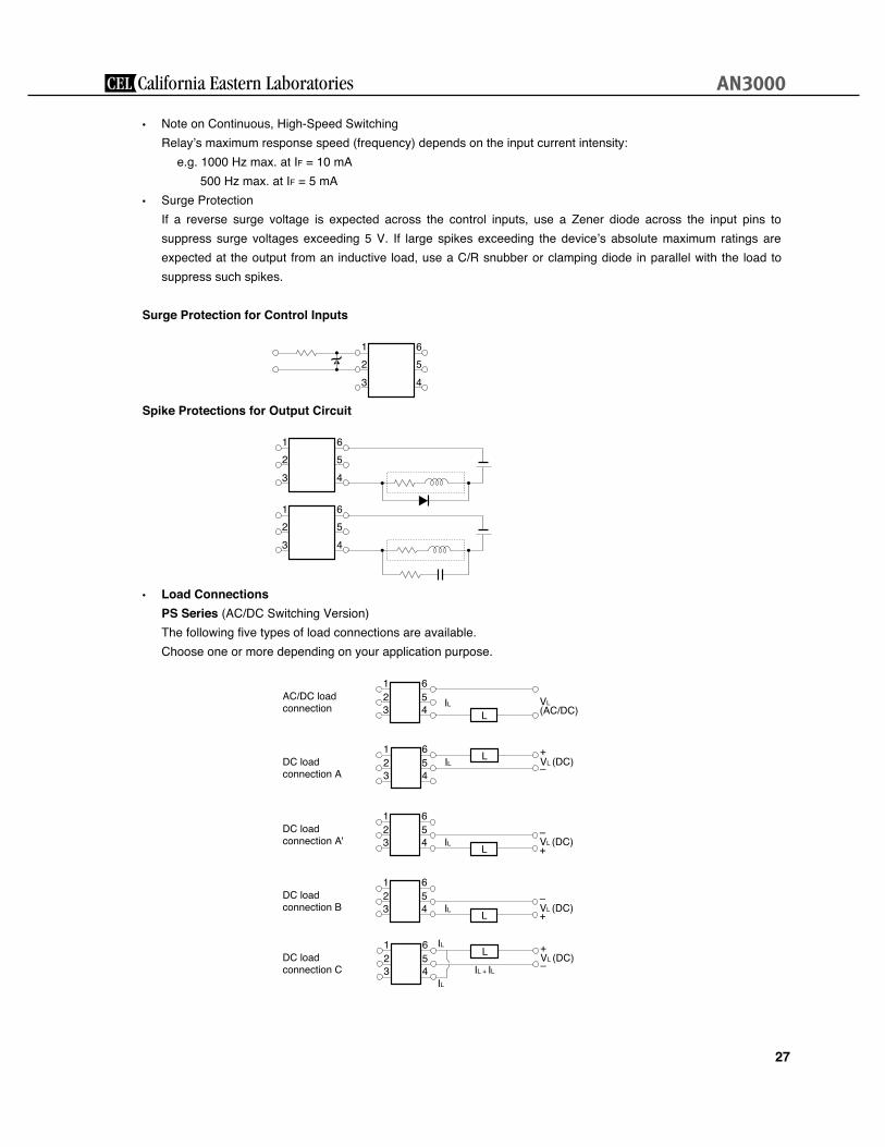
• Note on Continuous, High-Speed Switching
Relay’s maximum response speed (frequency) depends on the input current intensity:
e.g. 1000 Hz max. at IF = 10 mA
500 Hz max. at IF = 5 mA
• Surge Protection
If a reverse surge voltage is expected across the control inputs, use a Zener diode across the input pins to
suppress surge voltages exceeding 5 V. If large spikes exceeding the device’s absolute maximum ratings are
expected at the output from an inductive load, use a C/R snubber or clamping diode in parallel with the load to
suppress such spikes.
Surge Protection for Control Inputs
1
2
3
6
5
4
Spike Protections for Output Circuit
1
2
3
6
5
4
1
2
3
6
5
4
• Load Connections
PS Series (AC/DC Switching Version)
The following five types of load connections are available.
Choose one or more depending on your application purpose.
123
654 L
IL VL(AC/DC)
123
654
LIL VL (DC)
+
–
123
654
LIL VL (DC)
+
+
–
123
654
LIL VL (DC)
–
123
654
LVL (DC)
IL
ILIL + IL
+
–
AC/DC loadconnection
DC loadconnection A
DC loadconnection A'
DC loadconnection B
DC loadconnection C
AN3000

28
• Input-Output Short Circuit
If an input pin is shorted to an output pin while the OCMOS FET is active, it may cause permanent damage to the
internal circuitry. Take care never to short one to the other.
• Handling Precautions
• Electrostatic damage to OCMOS FET
The output OCMOS FET has a pin-to-pin electrostatic destruction voltage of 2000 V (test condition: 100 pF, 1.5k
ohms). Care must be taken to protect the device from static electricity exceeding this value.
• Lead strength
Never apply a bend stress of more than 500 grams to any lead as it may cause damage to the OCMOS FET
package and mar the device’s performance and/or reliability.
• Soldering
Observe the following soldering conditions:
Dip soldering:
Prebake condition: 165 ºC, Not longer than 60 sec.
Soldering condition: 260 ºC, Not longer than 10 sec.
Soldering with soldering iron:
Iron tip temperature: 280 to 300 ºC
Iron wattage: 30 to 60 watts
Soldering duration: Not longer than 5 sec.
• Post-installation cleaning
Observe the following cleaning requirements for OCMOS FET mounted on a PC board:
Recommended Not
recommended
Cleaning solvent Isopropyl alcohol
Ethylalcohol
Trichloroethane
Toluene
Xylene
Cleaning method Yes/No
oNmaetS
Ultrasonic Conditional yes
oNgnihsurB
Dipping in solvent Yes
AN3000

29
8. CONCLUSION
Demand for OCMOS FET featuring high sensitivity, low driving power, extremely low offset voltage in the on-state
and very small leak current in the off-state is steadily increasing.
At the same time, various problems will occur in their circuit design.
We hope this manual will be helpful in solving such problems.
AN3000
Your source for NEC RF, Microwave, Optoelectronic,& Fiber Optic Semiconductor Devices.
4590 Patrick Henry Drive, Santa Clara, CA 95054-1817 (408) 919-2500 • FAX (408) 988-0279 • Telex 34/6393
www.cel.com
© California Eastern Laboratories 01/04/2006
Information and data presented here is subject to change without notice. California Eastern Laboratories assumes no responsibility for the use of
any circuits described herein and makes no representations or warranties, expressed or implied, that such circuits are free from patent infringement.