Characteristics of multipoint-to-multipoint fixed wireless ...

4
3
1
2
DE
D
RE
R
6
7
A
B
5
4
2
3
DE
D
RE
R
12
11
A
B
10
9Y
Z
SN65MLVD202A, SN65MLVD205ASN65MLVD200A, SN65MLVD204A
Product
Folder
Sample &Buy
Technical
Documents
Tools &
Software
Support &Community
SN65MLVD200A, SN65MLVD202ASN65MLVD204A, SN65MLVD205A
SLLS573D –DECEMBER 2003–REVISED DECEMBER 2015
SN65MLVD20xx Multipoint-LVDS Line Driver and Receiver1 Features 2 Applications1• Low-Voltage Differential 30-Ω to 55-Ω Line Drivers • Low-Power, High-Speed, Short-Reach Alternative
and Receivers for Signaling Rates(1) up to to TIA/EIA-485100 Mbps, Clock Frequencies up to 50 MHz • Backplane or Cabled Multipoint Data and Clock
• Type-1 Receivers Incorporate 25 mV of TransmissionHysteresis (SN65MLVD200A, SN65MLVD202A) • Cellular Base Stations
• Type-2 Receivers Provide an Offset (100 mV) • Central Office SwitchesThreshold to Detect Open-Circuit and Idle-Bus • Network Switches and RoutersConditions (SN65MLVD204A, SN65MLVD205A)
• Meets or Exceeds the M-LVDS Standard 3 DescriptionTIA/EIA-899 for Multipoint Data Interchange The SN65MLVD20xx devices are multipoint low-
• Controlled Driver Output Voltage Transition Times voltage differential (M-LVDS) line drivers andreceivers that are optimized to operate at signalingfor Improved Signal Qualityrates up to 100 Mbps. All parts comply with the• –1 V to 3.4 V of Common-Mode Voltage Rangemultipoint low-voltage differential signaling (M-LVDS)Allows Data Transfer With 2 V of Ground Noise standard TIA/EIA-899.
• Bus Pins High Impedance When DisabledThe SN65MLVD20xx devices have enhancementsor VCC ≤ 1.5 Vover their predecessors. Improved features include• 200-Mbps Devices Available (SN65MLVD201, controlled slew rate on the driver output to help
SN65MLVD203, SN65MLVD206, SN65MLVD207) minimize reflections from unterminated stubs, which• Bus Pin ESD Protection Exceeds 8 kV results in better signal integrity. Additionally, 8-kV
ESD protection on the bus pins for more robustness.• Packages Available:The same footprint definition was maintained making– 8-Pin SOIC for an easy drop-in replacement for a system
SN65MLVD200A, SN65MLVD204A performance upgrade.– 14-Pin SOIC The devices are characterized for operation fromSN65MLVD202A, SN65MLVD205A –40°C to 85°C.
• Improved Alternatives to the SN65MLVD200,SN65MLVD202A, SN65MLVD204A, and Device Information(1)
SN65MLVD205A Devices PART NUMBER PACKAGE BODY SIZE (NOM)(1) The signaling rate of a line, is the number of voltage SN65MLVD200A
SOIC (8) 4.90 mm × 3.91 mmtransitions that are made per second expressed in the units SN65MLVD204Abps (bits per second).SN65MLVD202A
SOIC (14) 8.65 mm × 3.91 mmSN65MLVD205A
(1) For all available packages, see the orderable addendum atthe end of the data sheet.
Logic Diagrams (Positive Logic)
1
An IMPORTANT NOTICE at the end of this data sheet addresses availability, warranty, changes, use in safety-critical applications,intellectual property matters and other important disclaimers. PRODUCTION DATA.

SN65MLVD200A, SN65MLVD202ASN65MLVD204A, SN65MLVD205ASLLS573D –DECEMBER 2003–REVISED DECEMBER 2015 www.ti.com
Table of Contents9.1 Overview ................................................................. 161 Features .................................................................. 19.2 Functional Block Diagram ....................................... 162 Applications ........................................................... 19.3 Feature Description................................................. 163 Description ............................................................. 19.4 Device Functional Modes........................................ 174 Revision History..................................................... 2
10 Application and Implementation........................ 195 Device Comparison Table ..................................... 310.1 Application Information.......................................... 196 Pin Configuration and Functions ......................... 310.2 Typical Application ............................................... 197 Specifications......................................................... 4 11 Power Supply Recommendations ..................... 237.1 Absolute Maximum Ratings ...................................... 4
12 Layout................................................................... 237.2 ESD Ratings ............................................................ 412.1 Layout Guidelines ................................................. 237.3 Recommended Operating Conditions....................... 412.2 Layout Example .................................................... 277.4 Thermal Information .................................................. 4
13 Device and Documentation Support ................. 287.5 Electrical Characteristics........................................... 513.1 Documentation Support ........................................ 287.6 Electrical Characteristics – Driver ............................. 513.2 Related Links ........................................................ 287.7 Electrical Characteristics – Receiver ........................ 613.3 Community Resources.......................................... 297.8 Electrical Characteristics – BUS Input and Output ... 613.4 Trademarks ........................................................... 297.9 Switching Characteristics – Driver ............................ 713.5 Electrostatic Discharge Caution............................ 297.10 Switching Characteristics – Receiver...................... 713.6 Glossary ................................................................ 297.11 Typical Characteristics ............................................ 8
14 Mechanical, Packaging, and Orderable8 Parameter Measurement Information ................ 10Information ........................................................... 299 Detailed Description ............................................ 16
4 Revision History
Changes from Revision C (September 2015) to Revision D Page
• Deleted Features list item "Meets ±8-kV IEC 61000-4-2, Contact Discharge" ...................................................................... 1
Changes from Revision B (June 2015) to Revision C Page
• Deleted row "Open Circuit" from Table 3 and Table 4 as redundant .................................................................................. 17• Changed from "VID ≥ 50 mV " to "VID ≥ 150 mV " in Table 4 ............................................................................................... 17• Changed from "–50 mV < VID < 150 mV" to "50 mV < VID < 150 mV" in Table 4 ................................................................ 17
Changes from Revision A (December 2003) to Revision B Page
• Pin Configuration and Functions section, ESD Ratings table, Feature Description section, Device Functional Modes,Application and Implementation section, Power Supply Recommendations section, Layout section, Device andDocumentation Support section, and Mechanical, Packaging, and Orderable Information section ..................................... 1
• Removed SN65MLVD204B from the data sheet.................................................................................................................... 1• Changed Ordering Information to Device Comparison Table ................................................................................................ 3• Deleted |VID| MIN value in Recommended Operating Conditions .......................................................................................... 4• Changed Multipoint Configuration image ............................................................................................................................. 19
Changes from Original (December 2003) to Revision A Page
• Deleted duplicate Note from Figure 23 ................................................................................................................................ 14
2 Submit Documentation Feedback Copyright © 2003–2015, Texas Instruments Incorporated
Product Folder Links: SN65MLVD200A SN65MLVD202A SN65MLVD204A SN65MLVD205A

1
2
3
4
5
6
7
14
13
12
11
10
9
8
NC
R
RE
DE
D
GND
GND
VCC
VCC
A
B
Z
Y
NC
1
2
3
4
8
7
6
5
R
RE
DE
D
VCC
B
A
GND
SN65MLVD200A, SN65MLVD202ASN65MLVD204A, SN65MLVD205A
www.ti.com SLLS573D –DECEMBER 2003–REVISED DECEMBER 2015
5 Device Comparison Table
PART NUMBER FOOTPRINT RECEIVER TYPESN65MLVD200AD SN75176 Type 1SM65MLVD202AD SN75ALS180 Type 1SN65MLVD204AD SN75176 Type 2SM65MLVD205AD SN75ALS180 Type 2
6 Pin Configuration and Functions
D PackageD Package8-Pin SOIC
14-Pin SOICTop ViewTop View
Pin FunctionsPIN
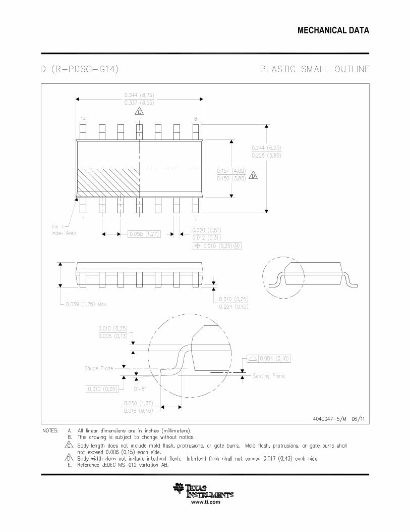
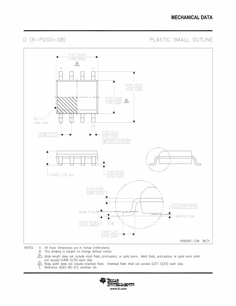
TYPE DESCRIPTIONNAME SOIC-8 SOIC-14A 6 12 I/O Differential I/OB 7 11 I/O Differential I/OD 4 5 I Driver inputDE 3 4 I Driver enable pin: High = Enable, Low = DisableGND 5 6, 7 Power Supply groundNC — 1, 8 NC No internal connectionR 1 2 O Receiver outputRE 2 3 I Receiver enable pin: High = Disable, Low = EnableVCC 8 13, 14 Power Power supply, 3.3 VY — 9 I/O Differential I/OZ — 10 I/O Differential I/O
Copyright © 2003–2015, Texas Instruments Incorporated Submit Documentation Feedback 3
Product Folder Links: SN65MLVD200A SN65MLVD202A SN65MLVD204A SN65MLVD205A
SN65MLVD200A, SN65MLVD202ASN65MLVD204A, SN65MLVD205ASLLS573D –DECEMBER 2003–REVISED DECEMBER 2015 www.ti.com
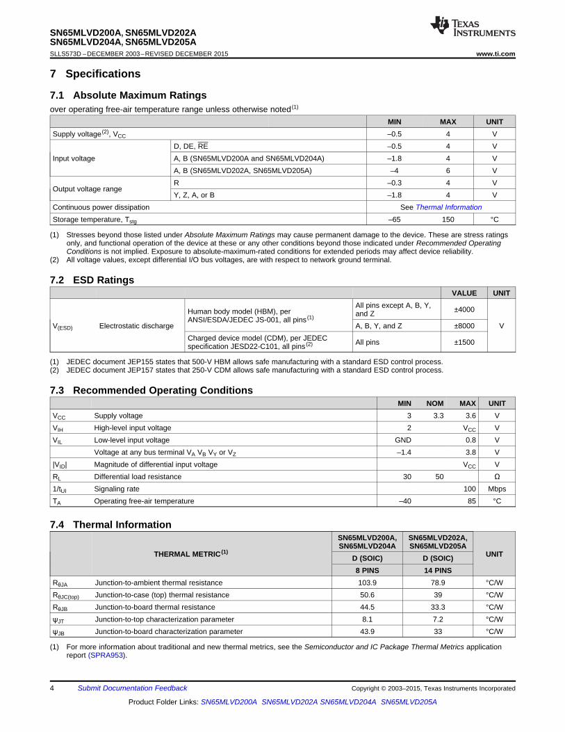
7 Specifications
7.1 Absolute Maximum Ratingsover operating free-air temperature range unless otherwise noted (1)
MIN MAX UNITSupply voltage (2), VCC –0.5 4 V
D, DE, RE –0.5 4 VInput voltage A, B (SN65MLVD200A and SN65MLVD204A) –1.8 4 V
A, B (SN65MLVD202A, SN65MLVD205A) –4 6 VR –0.3 4 V
Output voltage rangeY, Z, A, or B –1.8 4 V
Continuous power dissipation See Thermal InformationStorage temperature, Tstg –65 150 °C
(1) Stresses beyond those listed under Absolute Maximum Ratings may cause permanent damage to the device. These are stress ratingsonly, and functional operation of the device at these or any other conditions beyond those indicated under Recommended OperatingConditions is not implied. Exposure to absolute-maximum-rated conditions for extended periods may affect device reliability.
(2) All voltage values, except differential I/O bus voltages, are with respect to network ground terminal.
7.2 ESD RatingsVALUE UNIT
All pins except A, B, Y, ±4000Human body model (HBM), per and ZANSI/ESDA/JEDEC JS-001, all pins (1)
V(ESD) Electrostatic discharge A, B, Y, and Z ±8000 VCharged device model (CDM), per JEDEC All pins ±1500specification JESD22-C101, all pins (2)
(1) JEDEC document JEP155 states that 500-V HBM allows safe manufacturing with a standard ESD control process.(2) JEDEC document JEP157 states that 250-V CDM allows safe manufacturing with a standard ESD control process.
7.3 Recommended Operating ConditionsMIN NOM MAX UNIT
VCC Supply voltage 3 3.3 3.6 VVIH High-level input voltage 2 VCC VVIL Low-level input voltage GND 0.8 V
Voltage at any bus terminal VA VB VY or VZ –1.4 3.8 V|VID| Magnitude of differential input voltage VCC VRL Differential load resistance 30 50 Ω1/tUI Signaling rate 100 MbpsTA Operating free-air temperature –40 85 °C
7.4 Thermal InformationSN65MLVD200A, SN65MLVD202A,SN65MLVD204A SN65MLVD205A
THERMAL METRIC (1) UNITD (SOIC) D (SOIC)8 PINS 14 PINS
RθJA Junction-to-ambient thermal resistance 103.9 78.9 °C/WRθJC(top) Junction-to-case (top) thermal resistance 50.6 39 °C/WRθJB Junction-to-board thermal resistance 44.5 33.3 °C/WψJT Junction-to-top characterization parameter 8.1 7.2 °C/WψJB Junction-to-board characterization parameter 43.9 33 °C/W
(1) For more information about traditional and new thermal metrics, see the Semiconductor and IC Package Thermal Metrics applicationreport (SPRA953).
4 Submit Documentation Feedback Copyright © 2003–2015, Texas Instruments Incorporated
Product Folder Links: SN65MLVD200A SN65MLVD202A SN65MLVD204A SN65MLVD205A

SN65MLVD200A, SN65MLVD202ASN65MLVD204A, SN65MLVD205A
www.ti.com SLLS573D –DECEMBER 2003–REVISED DECEMBER 2015
7.5 Electrical Characteristicsover recommended operating conditions unless otherwise noted
PARAMETER TEST CONDITIONS MIN TYP (1) MAX UNITDriver only RE and DE at VCC, RL = 50 Ω, All others open 13 22Both disabled RE at VCC, DE at 0 V, RL = No Load, All others open 1 4
ICC Supply current mABoth enabled RE at 0 V, DE at VCC, RL = 50 Ω, All others open 16 24Receiver only RE at 0 V, DE at 0 V, All others open 4 13
RL = 50 Ω, Input to D is a 50-MHz 50% duty cycle squarePD Device power dissipation wave, 94 mW
DE = high, RE = low, TA = 85°C
(1) All typical values are at 25°C and with a 3.3-V supply voltage.
7.6 Electrical Characteristics – Driverover recommended operating conditions unless otherwise noted
PARAMETER TEST CONDITIONS MIN (1) TYP (2) MAX UNIT|VAB| or Differential output voltage magnitude 480 650 mV|VYZ|
See Figure 14Δ|VAB| or Change in differential output voltage magnitude –50 50 mVΔ|VYZ| between logic statesVOS(SS) Steady-state common-mode output voltage 0.8 1.2 V
Change in steady-state common-mode outputΔVOS(SS) See Figure 15 –50 50 mVvoltage between logic statesVOS(PP) Peak-to-peak common-mode output voltage 150 mVVY(OC) or Maximum steady-state open-circuit output voltage 0 2.4 VVA(OC) See Figure 19VZ(OC) or Maximum steady-state open-circuit output voltage 0 2.4 VVB(OC)
VP(H) Voltage overshoot, low-to-high level output 1.2 VSS VSee Figure 17
VP(L) Voltage overshoot, high-to-low level output –0.2 VSS VIIH High-level input current (D, DE) VIH = 2 V to VCC 0 10 µAIIL Low-level input current (D, DE) VIL = GND to 0.8 V 0 10 µA|IOS| Differential short-circuit output current magnitude See Figure 4 24 mA
–1.4 V ≤ (VY or VZ) ≤ 3.8 V,IOZ High-impedance state output current (driver only) –15 10 µAOther output = 1.2 V–1.4 V ≤ (VY or VZ) ≤ 3.8 V, OtherIO(OFF) Power-off output current –10 10 µAoutput = 1.2 V, 0 V ≤ VCC≤ 1.5 VVI = 0.4 sin(30E6πt) + 0.5 V, (3)
CY or CZ Output capacitance Other input at 1.2 V, driver 3 pFdisabledVAB = 0.4 sin(30E6πt) V, (3)
CYZ Differential output capacitance 2.5 pFDriver disabledCY/Z Output capacitance balance, (CY/CZ) 0.99 1.01
(1) The algebraic convention in which the least positive (most negative) limit is designated as minimum is used in this data sheet.(2) All typical values are at 25°C and with a 3.3-V supply voltage.(3) HP4194A impedance analyzer (or equivalent)
Copyright © 2003–2015, Texas Instruments Incorporated Submit Documentation Feedback 5
Product Folder Links: SN65MLVD200A SN65MLVD202A SN65MLVD204A SN65MLVD205A
SN65MLVD200A, SN65MLVD202ASN65MLVD204A, SN65MLVD205ASLLS573D –DECEMBER 2003–REVISED DECEMBER 2015 www.ti.com
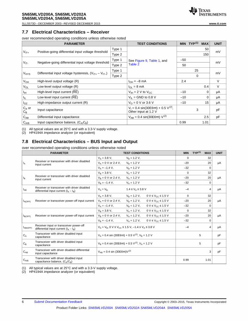
7.7 Electrical Characteristics – Receiverover recommended operating conditions unless otherwise noted
PARAMETER TEST CONDITIONS MIN TYP (1) MAX UNITType 1 50
VIT+ Positive-going differential input voltage threshold mVType 2 150Type 1 –50See Figure 9, Table 1, andVIT- Negative-going differential input voltage threshold mVTable 2Type 2 50Type 1 25
VHYS Differential input voltage hysteresis, (VIT+ – VIT–) mVType 2 0
VOH High-level output voltage (R) IOH = –8 mA 2.4 VVOL Low-level output voltage (R) IOL = 8 mA 0.4 VIIH High-level input current (RE) VIH = 2 V to VCC –10 0 µAIIL Low-level input current (RE) VIL = GND to 0.8 V –10 0 µAIOZ High-impedance output current (R) VO = 0 V or 3.6 V –10 15 µACA or VI = 0.4 sin(30E6πt) + 0.5 V (2),Input capacitance 3 pFCB Other input at 1.2 VCAB Differential input capacitance VAB = 0.4 sin(30E6πt) V (2) 2.5 pFCA/B Input capacitance balance, (CA/CB) 0.99 1.01
(1) All typical values are at 25°C and with a 3.3-V supply voltage.(2) HP4194A impedance analyzer (or equivalent)
7.8 Electrical Characteristics – BUS Input and Outputover recommended operating conditions unless otherwise noted
PARAMETER TEST CONDITIONS MIN TYP (1) MAX UNIT
VA = 3.8 V, VB = 1.2 V, 0 32Receiver or transceiver with driver disabledIA VA = 0 V or 2.4 V, VB = 1.2 V –20 20 µAinput current
VA = –1.4 V, VB = 1.2 V –32 0
VB = 3.8 V, VA = 1.2 V 0 32Receiver or transceiver with driver disabledIB VB = 0 V or 2.4 V, VA = 1.2 V –20 20 µAinput current
VB = –1.4 V, VA = 1.2 V –32 0
Receiver or transceiver with driver disabledIAB VA = VB, 1.4 ≤ VA ≤ 3.8 V –4 4 µAdifferential input current (IA – IB)
VA = 3.8 V, VB = 1.2 V, 0 V ≤ VCC ≤ 1.5 V 0 32
IA(OFF) Receiver or transceiver power-off input current VA = 0 V or 2.4 V, VB = 1.2 V, 0 V ≤ VCC ≤ 1.5 V –20 20 µA
VA = –1.4 V, VB = 1.2 V, 0 V ≤ VCC ≤ 1.5 V –32 0
VB = 3.8 V, VA = 1.2 V, 0 V ≤ VCC ≤ 1.5 V 0 32
IB(OFF) Receiver or transceiver power-off input current VB = 0 V or 2.4 V, VA = 1.2 V, 0 V ≤ VCC ≤ 1.5 V –20 20 µA
VB = –1.4 V, VA = 1.2 V, 0 V ≤ VCC ≤ 1.5 V –32 0
Receiver input or transceiver power-offIAB(OFF) VA = VB, 0 V ≤ VCC ≤ 1.5 V, –1.4 ≤ VA ≤ 3.8 V –4 4 µAdifferential input current (IA – IB)
Transceiver with driver disabled inputCA VA = 0.4 sin (30E6πt) + 0.5 V (2), VB = 1.2 V 5 pFcapacitance
Transceiver with driver disabled inputCB VB = 0.4 sin (30E6πt) + 0.5 V (2), VA = 1.2 V 5 pFcapacitance
Transceiver with driver disabled differentialCAB VAB = 0.4 sin (30E6πt)V (2) 3 pFinput capacitance
Transceiver with driver disabled inputCA/B 0.99 1.01capacitance balance, (CA/CB)
(1) All typical values are at 25°C and with a 3.3-V supply voltage.(2) HP4194A impedance analyzer (or equivalent)
6 Submit Documentation Feedback Copyright © 2003–2015, Texas Instruments Incorporated
Product Folder Links: SN65MLVD200A SN65MLVD202A SN65MLVD204A SN65MLVD205A

SN65MLVD200A, SN65MLVD202ASN65MLVD204A, SN65MLVD205A
www.ti.com SLLS573D –DECEMBER 2003–REVISED DECEMBER 2015
7.9 Switching Characteristics – Driverover recommended operating conditions unless otherwise noted
PARAMETER TEST CONDITIONS MIN TYP (1) MAX UNITtpLH Propagation delay time, low-to-high-level output 2 2.5 3.5 nstpHL Propagation delay time, high-to-low-level output 2 2.5 3.5 nstr Differential output signal rise time See Figure 17 2 2.6 3.2 nstf Differential output signal fall time 2 2.6 3.2 nstsk(p) Pulse skew (|tpHL – tpLH|) 30 150 pstsk(pp) Part-to-part skew (2) 0.9 nstjit(per) Period jitter, rms (1 standard deviation) (3) 50-MHz clock input (4) 2 3 pstjit(pp) Peak-to-peak jitter (3) (5) 100 Mbps 215 –1 PRBS input (6) 55 150 pstPHZ Disable time, high-level-to-high-impedance output 4 7 nstPLZ Disable time, low-level-to-high-impedance output 4 7 ns
See Figure 18tPZH Enable time, high-impedance-to-high-level output 4 7 nstPZL Enable time, high-impedance-to-low-level output 4 7 ns
(1) All typical values are at 25°C and with a 3.3-V supply voltage.(2) Part-to-part skew is defined as the difference in propagation delays between two devices that operate at the same V/T conditions.(3) Jitter is ensured by design and characterization. Stimulus jitter has been subtracted from the numbers.(4) tr = tf = 0.5 ns (10% to 90%), measured over 30K samples.(5) Peak-to-peak jitter includes jitter due to pulse skew (tsk(p)).(6) tr = tf = 0.5 ns (10% to 90%), measured over 100K samples.
7.10 Switching Characteristics – Receiverover recommended operating conditions unless otherwise noted
PARAMETER TEST CONDITIONS MIN TYP (1) MAX UNITtPLH Propagation delay time, low-to-high-level output 2 3.6 6 nstPHL Propagation delay time, high-to-low-level output 2 3.6 6 nstr Output signal rise time 1 2.3 nstf Output signal fall time CL = 15 pF, See Figure 22 1 2.3 ns
Type 1 100 300 pstsk(p) Pulse skew (|tpHL – tpLH|)
Type 2 300 500 pstsk(pp) Part-to-part skew (2) 1 nstjit(per) Period jitter, rms (1 standard deviation) (3) 50-MHz clock input (4) 4 7 ps
Type 1 200 700 pstjit(pp) Peak-to-peak jitter (3) (5) 100 Mbps 215 –1 PRBS input (6)
Type 2 225 800 pstPHZ Disable time, high-level-to-high-impedance output 6 10 nstPLZ Disable time, low-level-to-high-impedance output 6 10 ns
See Figure 23tPZH Enable time, high-impedance-to-high-level output 10 15 nstPZL Enable time, high-impedance-to-low-level output 10 15 ns
(1) All typical values are at 25°C and with a 3.3-V supply voltage.(2) Part-to-part skew is defined as the difference in propagation delays between two devices that operate at the same V/T conditions.(3) Jitter is ensured by design and characterization. Stimulus jitter has been subtracted from the numbers.(4) VID = 200 mVpp (MLVD200A, 202A), VID = 400 mVpp (MLVD204A, 205A), Vcm = 1 V, tr = tf = 0.5 ns (10% to 90%), measured over 30K
samples.(5) Peak-to-peak jitter includes jitter due to pulse skew (tsk(p))(6) VID = 200 mVpp (MLVD200A, 202A), VID = 400 mVpp (MLVD204A, 205A), Vcm = 1 V, tr = tf = 0.5 ns (10% to 90%), measured over 100K
samples.
Copyright © 2003–2015, Texas Instruments Incorporated Submit Documentation Feedback 7
Product Folder Links: SN65MLVD200A SN65MLVD202A SN65MLVD204A SN65MLVD205A

2
2.2
2.4
2.6
2.8
−40 −15 10 35 60 85
Driver
Pro
pagation D
ela
y−
ns
TA − Free-Air Temperature − °C
VCC = 3.3 V
f = 1 MHz
RL = 50 Ω
tpHL
tpLH
3
3.20
3.40
3.60
3.80
4
−40 −15 10 35 60 85
Receiv
er
Pro
pagation D
ela
y−
ns
TA − Free-Air Temperature − °C
VCC = 3.3 V
VID = 200 mV
VIC = 1 V
f = 1 MHz
CL = 15 pF
tpLH
tpHL
0
30
40
50
60
70
0 1 2 4
−R
eceiv
er
Low
Level O
utp
ut C
urr
ent−
mA
VOL − Low Level Output Voltage − V
3
I OL
10
20
VCC = 3.6 V
VCC = 3.3 V
VCC = 3.0 V
TA = 25°C
−90
−60
−50
−40
−30
−20
0 1 2 4
−R
eceiv
er
Hig
h L
evel O
utp
ut C
urr
ent−
mA
VOH − High Level Output Voltage − V
3
I OH
−80
−70
VCC = 3.0 V
−10
0
VCC = 3.6 V
VCC = 3.3 V
TA = 25°C
0
5
10
15
20
10 20 30 40 50
I
f − Frequency − MHz
−S
upply
Curr
ent−
mA
CC
TX
RX
VCC = 3.3 VVID = 200 mVVIC = 1 VTA = 25°C
0
5
10
15
20
25
30
−40 −15 10 35 60 85
I−
Supply
Curr
ent−
mA
CC
TA − Free-Air Temperature − °C
VCC = 3.3 Vf = 50 MHzVID = 200 mVVIC = 1 V
RX
TX
SN65MLVD200A, SN65MLVD202ASN65MLVD204A, SN65MLVD205ASLLS573D –DECEMBER 2003–REVISED DECEMBER 2015 www.ti.com
7.11 Typical Characteristics
Figure 1. Supply Current vs Frequency Figure 2. Supply Current vs Free-Air Temperature
Figure 4. Receiver High-Level Output CurrentFigure 3. Receiver Low-Level Output Currentvs High-Level Output Voltagevs Low-Level Output Voltage
Figure 6. Receiver Propagation DelayFigure 5. Driver Propagation Delay vs Free-Air Temperaturevs Free-Air Temperature
8 Submit Documentation Feedback Copyright © 2003–2015, Texas Instruments Incorporated
Product Folder Links: SN65MLVD200A SN65MLVD202A SN65MLVD204A SN65MLVD205A
0
60
120
180
240
300
−40 −15 10 35 60 85
TA − Free-Air Temperature − °C
Added
Receiv
er
Peak-T
o-P
eak
Jitte
r−
ps
Type-2VID = 400 mV
Type-1VID = 200 mV
VCC = 3.3 VVIC = 1 V
215-1 PRBS NRZ
0
60
120
180
240
300
20 40 60 80 100
Added
Receiv
er
Peak-T
o-P
eak
Jitte
r−
ps
Signaling Rate − Mbps
Type-2VID = 400 mV
Type-1VID = 200 mV
VCC = 3.3 VTA = 25 CVIC = 1 V
215-1 PRBS NRZ
40
48
56
64
72
80
−40 −15 10 35 60 85
Added
Driver
Peak-T
o-P
eak
Jitte
r−
ps
TA − Free-Air Temperature − °C
VCC = 3.3 V
VIC = 1 V
f = 100 Mbps
215-1 PRBS NRZ
10
16
22
28
34
40
10 20 30 40 50
Clock Frequency − MHz
Added R
eceiv
er
Cycle
-To-C
ycle
Jitte
r−
ps
VCC = 3.3 V
TA = 25°C
VIC = 1 V Type-1
VID = 200 mV
Type-2
VID = 400 mV
0
6
12
18
24
30
10 20 30 40 50
Clock Frequency − MHz
Added
Driver
Cycle
-To-C
ycle
Jitte
r−
ps
VCC = 3.3 V
TA = 25°C
Input = Clock
20
28
36
44
52
60
20 40 60 80 100
Signaling Rate − Mbps
Added
Driver
Peak-T
o-P
eak
Jitte
r−
ps
VCC = 3.3 V
TA = 25°C
215-1 PRBS NRZ
SN65MLVD200A, SN65MLVD202ASN65MLVD204A, SN65MLVD205A
www.ti.com SLLS573D –DECEMBER 2003–REVISED DECEMBER 2015
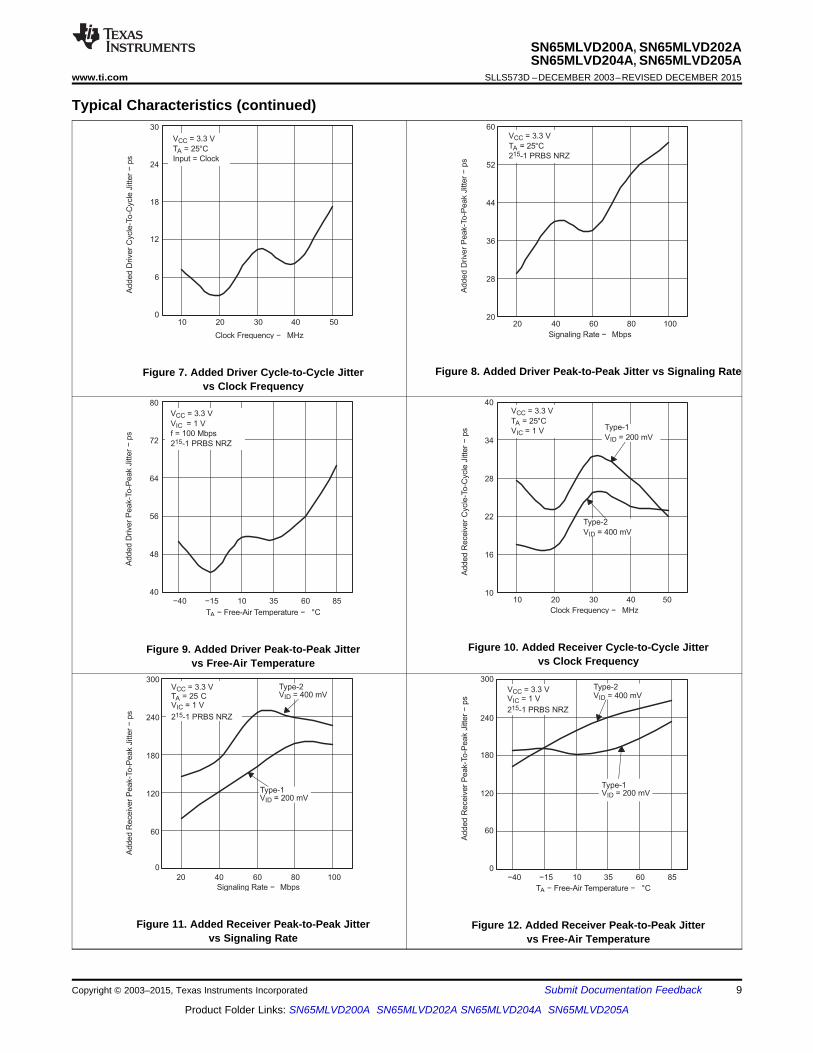
Typical Characteristics (continued)
Figure 8. Added Driver Peak-to-Peak Jitter vs Signaling RateFigure 7. Added Driver Cycle-to-Cycle Jittervs Clock Frequency
Figure 10. Added Receiver Cycle-to-Cycle JitterFigure 9. Added Driver Peak-to-Peak Jittervs Clock Frequencyvs Free-Air Temperature
Figure 11. Added Receiver Peak-to-Peak Jitter Figure 12. Added Receiver Peak-to-Peak Jittervs Signaling Rate vs Free-Air Temperature
Copyright © 2003–2015, Texas Instruments Incorporated Submit Documentation Feedback 9
Product Folder Links: SN65MLVD200A SN65MLVD202A SN65MLVD204A SN65MLVD205A

VTest
+
-
A/Y
B/Z
IOS
0 V or VCC
-1 V or 3.4 V
VOS
R124.9 Ω
A/Y
C32.5 pF
VOS(PP) VOS(SS)
VOS(SS)
≈ 1.3 V
B/Z
A/Y
≈ 0.7 V
B/Z
D
R224.9 Ω
C11 pF
C21 pF
VAB or VYZ 49.9 Ω
3.32 kΩ
3.32 kΩ
_+ -1 V ≤ Vtest ≤ 3.4 V
A/Y
B/Z
D
VAB or VYZ
A/Y
B/Z
IA or IY
VB or VZ
VA or VYVOS
VA + VB
2
VI
D
VCC
VY + VZ
2or
IB or IZ
II
SN65MLVD200A, SN65MLVD202ASN65MLVD204A, SN65MLVD205ASLLS573D –DECEMBER 2003–REVISED DECEMBER 2015 www.ti.com
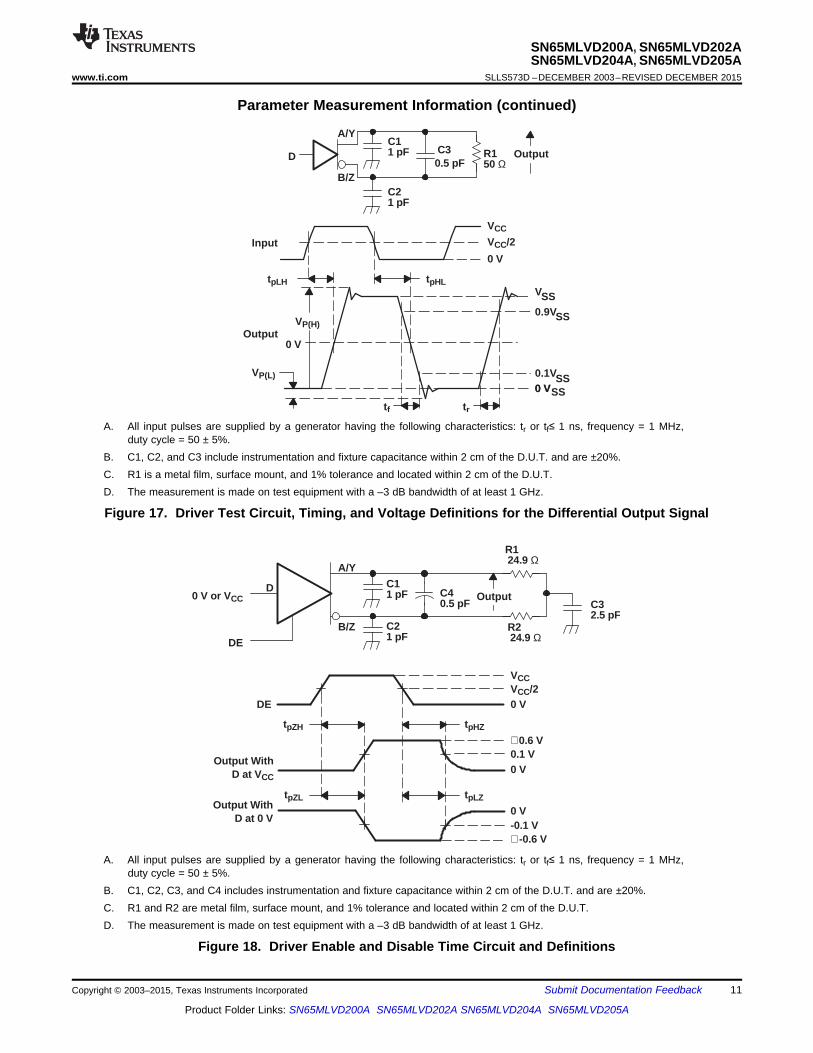
8 Parameter Measurement Information
Figure 13. Driver Voltage and Current Definitions
A. All resistors are 1% tolerance.
Figure 14. Differential Output Voltage Test Circuit
A. All input pulses are supplied by a generator having the following characteristics: tr or tf≤ 1 ns,pulse frequency = 1 MHz, duty cycle = 50 ± 5%.
B. C1, C2 and C3 include instrumentation and fixture capacitance within 2 cm of the D.U.T. and are ±20%.C. R1 and R2 are metal film, surface mount, ±1%, and located within 2 cm of the D.U.T.D. The measurement of VOS(PP) is made on test equipment with a –3 dB bandwidth of at least 1 GHz.
Figure 15. Test Circuit and Definitions for the Driver Common-Mode Output Voltage
Figure 16. Driver Short-Circuit Test Circuit
10 Submit Documentation Feedback Copyright © 2003–2015, Texas Instruments Incorporated
Product Folder Links: SN65MLVD200A SN65MLVD202A SN65MLVD204A SN65MLVD205A
A/Y
B/Z
R124.9 Ω
tpZH tpHZ
tpZL tpLZ
VCCVCC/20 V
∼ 0.6 V0.1 V0 V
∼ -0.6 V
0 V-0.1 V
DE
Output WithD at VCC
Output0 V or VCC
DE
Output WithD at 0 V
C11 pF
R224.9 Ω
C40.5 pF
C21 pF
D
C32.5 pF
Output
A/Y
Output
tpLH tpHL
Input
C30.5 pF
B/Z
D
0 V
0.9V
V
0 V
tf tr
VCC
VCC/2
0 V
SS
SS0 V0.1VSS
SS
C11 pF
C21 pF
VP(H)
VP(L)
R150 Ω
SN65MLVD200A, SN65MLVD202ASN65MLVD204A, SN65MLVD205A
www.ti.com SLLS573D –DECEMBER 2003–REVISED DECEMBER 2015
Parameter Measurement Information (continued)
A. All input pulses are supplied by a generator having the following characteristics: tr or tf≤ 1 ns, frequency = 1 MHz,duty cycle = 50 ± 5%.
B. C1, C2, and C3 include instrumentation and fixture capacitance within 2 cm of the D.U.T. and are ±20%.C. R1 is a metal film, surface mount, and 1% tolerance and located within 2 cm of the D.U.T.D. The measurement is made on test equipment with a –3 dB bandwidth of at least 1 GHz.
Figure 17. Driver Test Circuit, Timing, and Voltage Definitions for the Differential Output Signal
A. All input pulses are supplied by a generator having the following characteristics: tr or tf≤ 1 ns, frequency = 1 MHz,duty cycle = 50 ± 5%.
B. C1, C2, C3, and C4 includes instrumentation and fixture capacitance within 2 cm of the D.U.T. and are ±20%.C. R1 and R2 are metal film, surface mount, and 1% tolerance and located within 2 cm of the D.U.T.D. The measurement is made on test equipment with a –3 dB bandwidth of at least 1 GHz.
Figure 18. Driver Enable and Disable Time Circuit and Definitions
Copyright © 2003–2015, Texas Instruments Incorporated Submit Documentation Feedback 11
Product Folder Links: SN65MLVD200A SN65MLVD202A SN65MLVD204A SN65MLVD205A

(VA + VB)/2
IOR
VCM VO
VID
VA
IAA
B
IBVB
tc(n)
1/f0
0 V
0 V
Period Jitter
0 V Diff
Peak to Peak Jitter
1/f0
PRBS INPUT
OUTPUT
VA -VB or VY -VZ
VA -VB or VY -VZ
CLOCKINPUT
IDEALOUTPUT
ACTUALOUTPUT
VCC
VCC/2
tjit(per) = tc(n) -1/f0tjit(pp)
0 V
VCC
VCC/2
0 V
VA -VB or VY -VZ
VA -VB or VY -VZ
A/Y
B/Z
0 V or VCC
1.62 kΩ , ±1%VA, VB, VY or VZ
SN65MLVD200A, SN65MLVD202ASN65MLVD204A, SN65MLVD205ASLLS573D –DECEMBER 2003–REVISED DECEMBER 2015 www.ti.com
Parameter Measurement Information (continued)
Figure 19. Maximum Steady State Output Voltage
A. All input pulses are supplied by an Agilent 81250 Stimulus System.B. The measurement is made on a TEK TDS6604 running TDSJIT3 application softwareC. Period jitter is measured using a 50 MHz 50 ±1% duty cycle clock input.D. Peak-to-peak jitter is measured using a 100 Mbps 215 –1 PRBS input.
Figure 20. Driver Jitter Measurement Waveforms
Figure 21. Receiver Voltage and Current Definitions
12 Submit Documentation Feedback Copyright © 2003–2015, Texas Instruments Incorporated
Product Folder Links: SN65MLVD200A SN65MLVD202A SN65MLVD204A SN65MLVD205A
1.2 V
1.0 V
tpLH
0.2 V
-0.2 V
VA
VB
VID
90%VOH
VOL
tpHL
10%
tf tr
VO
VCC/2
VO
VID
VB
VA CL
0 V
15 pF
SN65MLVD200A, SN65MLVD202ASN65MLVD204A, SN65MLVD205A
www.ti.com SLLS573D –DECEMBER 2003–REVISED DECEMBER 2015
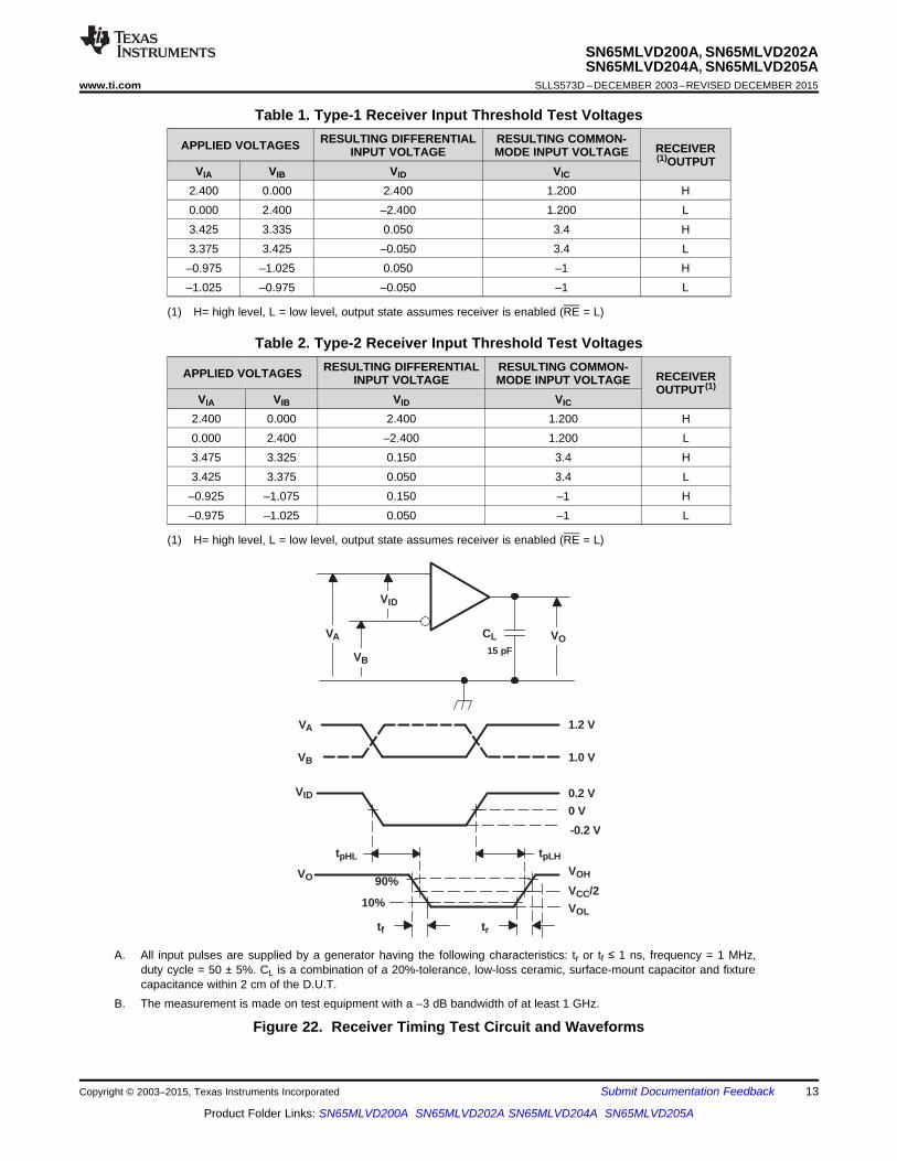
Table 1. Type-1 Receiver Input Threshold Test VoltagesRESULTING DIFFERENTIAL RESULTING COMMON-APPLIED VOLTAGES RECEIVERINPUT VOLTAGE MODE INPUT VOLTAGE (1)OUTPUT
VIA VIB VID VIC
2.400 0.000 2.400 1.200 H0.000 2.400 –2.400 1.200 L3.425 3.335 0.050 3.4 H3.375 3.425 –0.050 3.4 L–0.975 –1.025 0.050 –1 H–1.025 –0.975 –0.050 –1 L
(1) H= high level, L = low level, output state assumes receiver is enabled (RE = L)
Table 2. Type-2 Receiver Input Threshold Test VoltagesRESULTING DIFFERENTIAL RESULTING COMMON-APPLIED VOLTAGES RECEIVERINPUT VOLTAGE MODE INPUT VOLTAGE
OUTPUT (1)VIA VIB VID VIC
2.400 0.000 2.400 1.200 H0.000 2.400 –2.400 1.200 L3.475 3.325 0.150 3.4 H3.425 3.375 0.050 3.4 L
–0.925 –1.075 0.150 –1 H–0.975 –1.025 0.050 –1 L
(1) H= high level, L = low level, output state assumes receiver is enabled (RE = L)
A. All input pulses are supplied by a generator having the following characteristics: tr or tf ≤ 1 ns, frequency = 1 MHz,duty cycle = 50 ± 5%. CL is a combination of a 20%-tolerance, low-loss ceramic, surface-mount capacitor and fixturecapacitance within 2 cm of the D.U.T.
B. The measurement is made on test equipment with a –3 dB bandwidth of at least 1 GHz.
Figure 22. Receiver Timing Test Circuit and Waveforms
Copyright © 2003–2015, Texas Instruments Incorporated Submit Documentation Feedback 13
Product Folder Links: SN65MLVD200A SN65MLVD202A SN65MLVD204A SN65MLVD205A

15 pF
tpZL tpLZ
VOL
VOL +0.5 V
VO
RL499 Ω
_+ VTEST
B
A
RE
1.2 V
Inputs
VCC
1 V
VCC
VCC/20 V
VCCVCC/2
VTEST
A
RE
R
0 V
1.4 VA
tpZH tpHZ
0 V
VOH -0.5 V
VCC
VCC/20 V
VOH
VCC/2
RE
VO
R
Output
VTEST
CL
SN65MLVD200A, SN65MLVD202ASN65MLVD204A, SN65MLVD205ASLLS573D –DECEMBER 2003–REVISED DECEMBER 2015 www.ti.com
A. All input pulses are supplied by a generator having the following characteristics: tr or tf ≤ 1 ns, frequency = 1 MHz,duty cycle = 50 ± 5%.
B. RL is 1% tolerance, metal film, surface mount, and located within 2 cm of the D.U.T.C. CL is the instrumentation and fixture capacitance within 2 cm of the DUT and ±20%.
Figure 23. Receiver Enable and Disable Time Test Circuit and Waveforms
14 Submit Documentation Feedback Copyright © 2003–2015, Texas Instruments Incorporated
Product Folder Links: SN65MLVD200A SN65MLVD202A SN65MLVD204A SN65MLVD205A

tc(n)
1/f0
Period Jitter
Peak to Peak Jitter
1/f0
PRBS INPUT
OUTPUT
CLOCK INPUT
IDEALOUTPUT
ACTUALOUTPUT
tjit(per) = tc(n) -1/f0tjit(pp)
VA -VB
INPUTSVA -VB0.2 V - Type 10.4 V - Type 2
VIC1 V
VOH
VCC/2
VOL
VOH
VOL
VCC/2VOH
VOL
VCC/2
VA
VB
SN65MLVD200A, SN65MLVD202ASN65MLVD204A, SN65MLVD205A
www.ti.com SLLS573D –DECEMBER 2003–REVISED DECEMBER 2015
A. All input pulses are supplied by an Agilent 8304A Stimulus System.B. The measurement is made on a TEK TDS6604 running TDSJIT3 application softwareC. Period jitter is measured using a 50 MHz 50 ±1% duty cycle clock input.D. Peak-to-peak jitter is measured using a 100 Mbps 215 –1 PRBS input.
Figure 24. Receiver Jitter Measurement Waveforms
Copyright © 2003–2015, Texas Instruments Incorporated Submit Documentation Feedback 15
Product Folder Links: SN65MLVD200A SN65MLVD202A SN65MLVD204A SN65MLVD205A
4
3
1
2
DE
D
RE
R
6
7
A
B
5
4
2
3
DE
D
RE
R
12
11
A
B
10
9Y
Z
SN65MLVD202A, SN65MLVD205ASN65MLVD200A, SN65MLVD204A
SN65MLVD200A, SN65MLVD202ASN65MLVD204A, SN65MLVD205ASLLS573D –DECEMBER 2003–REVISED DECEMBER 2015 www.ti.com
9 Detailed Description
9.1 OverviewThe SN65MLVD20xA family of devices are multipoint-low-voltage differential (M-LVDS) line drivers and receiversthat are optimized to operate at signaling rates up to 100 Mbps. All parts comply with the multipoint low-voltagedifferential signaling (M-LVDS) standard TIA/EIA-899. These circuits are similar to their TIA/EIA-644 standardcompliant LVDS counterparts with added features to address multipoint applications. The driver output has beendesigned to support multipoint buses presenting loads as low as 30 Ω and incorporates controlled transitiontimes to allow for stubs off of the backbone transmission line.
These devices have Type-1 and Type-2 receivers that detect the bus state with as little as 50 mV (for Type-1) or150 mV (for Type-2) of differential input voltage over a common-mode voltage range of –1 V to 3.4 V. The Type-1 receivers exhibit 25 mV of differential input voltage hysteresis to prevent output oscillations with slowlychanging signals or loss of input. Type-2 receivers include an offset threshold to provide a known output stateunder open-circuit and bus-idle fault conditions.
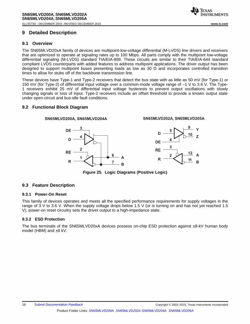
9.2 Functional Block Diagram
Figure 25. Logic Diagrams (Positive Logic)
9.3 Feature Description
9.3.1 Power-On ResetThis family of devices operates and meets all the specified performance requirements for supply voltages in therange of 3 V to 3.6 V. When the supply voltage drops below 1.5 V (or is turning on and has not yet reached 1.5V), power-on reset circuitry sets the driver output to a high-impedance state.
9.3.2 ESD ProtectionThe bus terminals of the SN65MLVD20xA devices possess on-chip ESD protection against ±8-kV human bodymodel (HBM) and ±8 kV.
16 Submit Documentation Feedback Copyright © 2003–2015, Texas Instruments Incorporated
Product Folder Links: SN65MLVD200A SN65MLVD202A SN65MLVD204A SN65MLVD205A

SN65MLVD200A, SN65MLVD202ASN65MLVD204A, SN65MLVD205A
www.ti.com SLLS573D –DECEMBER 2003–REVISED DECEMBER 2015
9.4 Device Functional Modes
9.4.1 Device Function Tables
Table 3. Type-1 Receiver (SN65MLVD200A) (1)
INPUTS OUTPUTVID = VA - VB RE RVID ≥ 50 mV L H
–50 mV < VID < 50 mV L ?VID ≤ –50 mV L L
X H ZX Open Z
(1) H = high level, L = low level, Z = high impedance, X = Don't care, ? = indeterminate
Table 4. Type-2 Receiver (SN65MLVD204A) (1)
INPUTS OUTPUTVID = VA - VB RE RVID ≥ 150 mV L H
50 mV < VID < 150 mV L ?VID ≤ 50 mV L L
X H ZX Open Z
(1) H = high level, L = low level, Z = high impedance, X = Don't care, ? = indeterminate
Table 5. Driver (1)
INPUTS ENABLE OUTPUTSD DE A BL H L HH H H L
Open H L HX Open Z ZX L Z Z
(1) H = high level, L = low level, Z = high impedance, X = Don't care, ? = indeterminate
Copyright © 2003–2015, Texas Instruments Incorporated Submit Documentation Feedback 17
Product Folder Links: SN65MLVD200A SN65MLVD202A SN65MLVD204A SN65MLVD205A

360 kΩ
400 Ω
VCC
DRIVER INPUT AND DRIVER ENABLE
D or DE
7 V
400 Ω
VCC
RE
7 V
RECEIVER ENABLE
VCC
7 V
10 Ω
10 Ω
RECEIVER OUTPUT
360 kΩ
DRIVER OUTPUT
A/Y or B/Z
R
VCC
200 kΩ
250 kΩ
200 kΩ
250 kΩ
100 kΩ100 kΩ
VCC
RECEIVER INPUT
BA
SN65MLVD200A, SN65MLVD202ASN65MLVD204A, SN65MLVD205ASLLS573D –DECEMBER 2003–REVISED DECEMBER 2015 www.ti.com
9.4.2 Equivalent Input and Output Schematic Diagrams
18 Submit Documentation Feedback Copyright © 2003–2015, Texas Instruments Incorporated
Product Folder Links: SN65MLVD200A SN65MLVD202A SN65MLVD204A SN65MLVD205A

RD
RD
RD
RD
~100 Ω~ ~100 Ω~
SN65MLVD200A, SN65MLVD202ASN65MLVD204A, SN65MLVD205A
www.ti.com SLLS573D –DECEMBER 2003–REVISED DECEMBER 2015
10 Application and Implementation
NOTEInformation in the following applications sections is not part of the TI componentspecification, and TI does not warrant its accuracy or completeness. TI’s customers areresponsible for determining suitability of components for their purposes. Customers shouldvalidate and test their design implementation to confirm system functionality.
10.1 Application InformationThe SN65MLVD20xA family of devices are multipoint line drivers and receivers. The functionality of thesedevices is simple, yet extremely flexible, thus leading to their use in designs ranging from wireless base stationsto desktop computers.
10.2 Typical ApplicationFigure 26 shows a multipoint configuration. In a multipoint configuration, many transmitters and many receiverscan be interconnected on one transmission line. The key difference compared to multidrop is the presence of twoor more drivers. Such a situation creates contention issues that must not be addressed with point-to-point ormultidrop systems. Multipoint operation allows for bidirectional, half-duplex communication over one balancedmedia pair. To support the location of the various drivers throughout the transmission line, double termination ofthe transmission line is now necessary.
The major challenge that system designers encounter are the impedance discontinuities that device loading anddevice connections (stubs) introduce on the common bus. Matching the impedance of the loaded bus and usingsignal drivers with controlled signal edges are the keys to error-free signal transmissions in multipoint topologies.
Figure 26. Multipoint Configuration
10.2.1 Design RequirementsFor this design example, use the parameters listed in Table 6.
Table 6. Design ParametersPARAMETERS VALUES
Driver supply voltage 3 V to 3.6 VDriver input voltage 0.8 V to 3.3 VDriver signaling rate DC to 100 MbpsInterconnect characteristic impedance 100 Ω(differential)Termination resistance 100 ΩNumber of receiver nodes 2 to 32Receiver supply voltage 3 V to 3.6 VReceiver input voltage 0 to (VCC – 0.8) VReceiver signaling rate DC to 100 MbpsGround shift between driver and ±1 Vreceiver
Copyright © 2003–2015, Texas Instruments Incorporated Submit Documentation Feedback 19
Product Folder Links: SN65MLVD200A SN65MLVD202A SN65MLVD204A SN65MLVD205A
0.1 µF 0.004 µF
3.3 V
MLVDS
100 mAC 4ns 0.004 F
100 mV
æ ö= ´ = mç ÷
è ø
Maximum Step Change Supply Currentchip Rise Time
Maximum Power Supply Noise
IC T
V
æ öD= ´ç ÷
ç ÷Dè ø
SN65MLVD200A, SN65MLVD202ASN65MLVD204A, SN65MLVD205ASLLS573D –DECEMBER 2003–REVISED DECEMBER 2015 www.ti.com
10.2.2 Detailed Design Procedure
10.2.2.1 Supply VoltageThe SN65MLVD20xA devices are operated from one supply. The SN65MLVD20xA devices can supportoperation with a supply as low as 3 V and as high as 3.6 V.
10.2.2.2 Supply Bypass CapacitanceBypass capacitors play a key role in power distribution circuitry. At low frequencies, power supply offers very low-impedance paths between its terminals. However, as higher frequency currents propagate through power traces,the source is often incapable of maintaining a low-impedance path to ground. Bypass capacitors are used toaddress this shortcoming. Usually, large bypass capacitors (10 μF to 1000 μF) at the board level do a good jobup into the kHz range. Due to their size and length of their leads, large capacitors tend to have large inductancevalues at the switching frequencies. To solve this problem, smaller capacitors (in the nF to μF range) must beinstalled locally next to the integrated circuit.
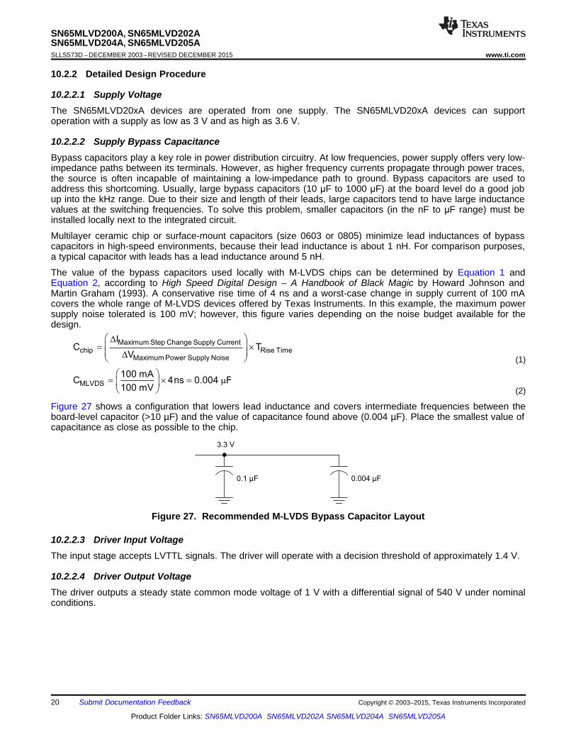
Multilayer ceramic chip or surface-mount capacitors (size 0603 or 0805) minimize lead inductances of bypasscapacitors in high-speed environments, because their lead inductance is about 1 nH. For comparison purposes,a typical capacitor with leads has a lead inductance around 5 nH.
The value of the bypass capacitors used locally with M-LVDS chips can be determined by Equation 1 andEquation 2, according to High Speed Digital Design – A Handbook of Black Magic by Howard Johnson andMartin Graham (1993). A conservative rise time of 4 ns and a worst-case change in supply current of 100 mAcovers the whole range of M-LVDS devices offered by Texas Instruments. In this example, the maximum powersupply noise tolerated is 100 mV; however, this figure varies depending on the noise budget available for thedesign.
(1)
(2)
Figure 27 shows a configuration that lowers lead inductance and covers intermediate frequencies between theboard-level capacitor (>10 µF) and the value of capacitance found above (0.004 µF). Place the smallest value ofcapacitance as close as possible to the chip.
Figure 27. Recommended M-LVDS Bypass Capacitor Layout
10.2.2.3 Driver Input VoltageThe input stage accepts LVTTL signals. The driver will operate with a decision threshold of approximately 1.4 V.
10.2.2.4 Driver Output VoltageThe driver outputs a steady state common mode voltage of 1 V with a differential signal of 540 V under nominalconditions.
20 Submit Documentation Feedback Copyright © 2003–2015, Texas Instruments Incorporated
Product Folder Links: SN65MLVD200A SN65MLVD202A SN65MLVD204A SN65MLVD205A

-100
-50
0
50
100
150
200Type 1
Transition Regions
Type 2
Low
High
Low
High
Diff
ere
ntial In
put
Voltage
(m
V)
SN65MLVD200A, SN65MLVD202ASN65MLVD204A, SN65MLVD205A
www.ti.com SLLS573D –DECEMBER 2003–REVISED DECEMBER 2015
10.2.2.5 Termination ResistorsAn M-LVDS communication channel employs a current source driving a transmission line that is terminated withtwo resistive loads. These loads serve to convert the transmitted current into a voltage at the receiver input. Toensure good signal integrity, the termination resistors must be matched to the characteristic impedance of thetransmission line. The designer must ensure that the termination resistors are within 10% of the nominal mediacharacteristic impedance. If the transmission line is targeted for 100-Ω impedance, the termination resistors mustbe between 90 Ω and 110 Ω. The line termination resistors are typically placed at the ends of the transmissionline.
10.2.2.6 Receiver Input SignalThe M-LVDS receivers herein comply with the M-LVDS standard and correctly determine the bus state. Thesedevices have Type-1 and Type-2 receivers that detect the bus state with as little as 50 mV of differential voltageover the common mode range of –1 V to 3.4 V.
10.2.2.7 Receiver Input Threshold (Failsafe)The M-LVDS standard defines a Type-1 and a Type-2 receiver. Type-1 receivers have differential input voltagethresholds near zero volts. Type-2 receivers have differential input voltage thresholds offset from 0 V to detectthe absence of a voltage difference. The impact to receiver output by the offset input can be seen in Table 7 andFigure 28.
Table 7. Receiver Input Voltage Threshold RequirementsRECEIVER TYPE OUTPUT LOW OUTPUT HIGH
Type 1 –2.4 V ≤ VID ≤ –0.05 V 0.05 V ≤ VID ≤ 2.4 VType 2 –2.4 V ≤ VID ≤ 0.05 V 0.15 V ≤ VID ≤ 2.4 V
Figure 28. Expanded Graph of Receiver Differential Input Voltage Showing Transition Region
10.2.2.8 Receiver Output SignalReceiver outputs comply with LVTTL output voltage standards when the supply voltage is within the range of 3 Vto 3.6 V.
10.2.2.9 Interconnecting MediaThe physical communication channel between the driver and the receiver may be any balanced, paired metalconductors that meet the requirements of the M-LVDS standard—the key points are included in the following.The interconnecting media may be a twisted pair, twinax, flat ribbon cable, or PCB traces.
The nominal characteristic impedance of the interconnect must be between 100 Ω and 120 Ω with variation nomore than 10% (90 Ω to 132 Ω).
Copyright © 2003–2015, Texas Instruments Incorporated Submit Documentation Feedback 21
Product Folder Links: SN65MLVD200A SN65MLVD202A SN65MLVD204A SN65MLVD205A
0r
87 5.98 HZ ln
0.8 W T1.41
§ · ¨ ¸H © ¹
> @> @0
r
1.9 2 H T60Z ln
0.8 W T
§ · ¨ ¸¨ ¸H © ¹
s0.96
Hdiff 0Z 2 Z 1 0.48 e
u§ ·¨ ¸ u u u¨ ¸© ¹
s2.9
Hdiff 0Z 2 Z 1 0.347 e
u§ ·¨ ¸ u u u¨ ¸© ¹
Co-Planar Coupled Microstrips Broad-Side Coupled Striplines
Edge-Coupled Edge-Coupled
Single-Ended Microstrip Single-Ended Stripline
W
H
T
W
TH
H
S
H
Differential Microstrip Differential Stripline
S
H
S
H
HG G
W W W
S
SN65MLVD200A, SN65MLVD202ASN65MLVD204A, SN65MLVD205ASLLS573D –DECEMBER 2003–REVISED DECEMBER 2015 www.ti.com
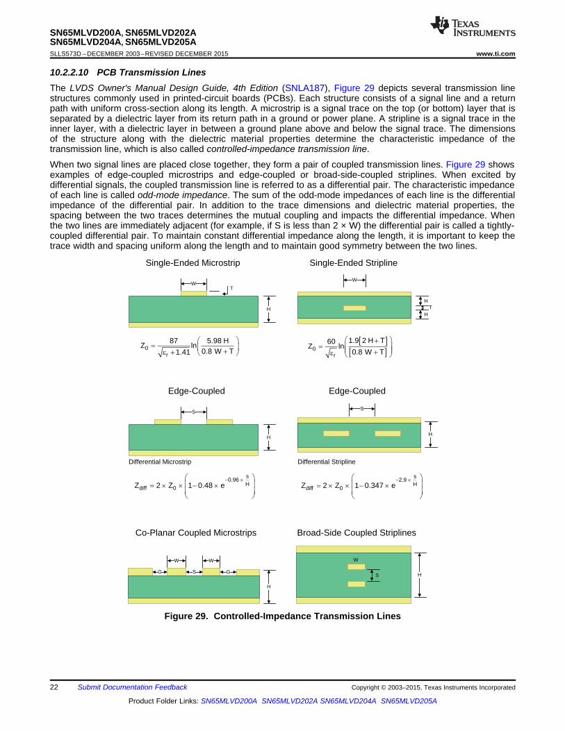
10.2.2.10 PCB Transmission LinesThe LVDS Owner's Manual Design Guide, 4th Edition (SNLA187), Figure 29 depicts several transmission linestructures commonly used in printed-circuit boards (PCBs). Each structure consists of a signal line and a returnpath with uniform cross-section along its length. A microstrip is a signal trace on the top (or bottom) layer that isseparated by a dielectric layer from its return path in a ground or power plane. A stripline is a signal trace in theinner layer, with a dielectric layer in between a ground plane above and below the signal trace. The dimensionsof the structure along with the dielectric material properties determine the characteristic impedance of thetransmission line, which is also called controlled-impedance transmission line.
When two signal lines are placed close together, they form a pair of coupled transmission lines. Figure 29 showsexamples of edge-coupled microstrips and edge-coupled or broad-side-coupled striplines. When excited bydifferential signals, the coupled transmission line is referred to as a differential pair. The characteristic impedanceof each line is called odd-mode impedance. The sum of the odd-mode impedances of each line is the differentialimpedance of the differential pair. In addition to the trace dimensions and dielectric material properties, thespacing between the two traces determines the mutual coupling and impacts the differential impedance. Whenthe two lines are immediately adjacent (for example, if S is less than 2 × W) the differential pair is called a tightly-coupled differential pair. To maintain constant differential impedance along the length, it is important to keep thetrace width and spacing uniform along the length and to maintain good symmetry between the two lines.
Figure 29. Controlled-Impedance Transmission Lines
22 Submit Documentation Feedback Copyright © 2003–2015, Texas Instruments Incorporated
Product Folder Links: SN65MLVD200A SN65MLVD202A SN65MLVD204A SN65MLVD205A
Horizontal Scale = 2 ns/div
Vert
ical S
cale
= 1
27.2
mV
/div
Horizontal Scale = 2 ns/div
Vert
ical S
cale
= 4
00 m
V/d
iv
SN65MLVD200A, SN65MLVD202ASN65MLVD204A, SN65MLVD205A
www.ti.com SLLS573D –DECEMBER 2003–REVISED DECEMBER 2015
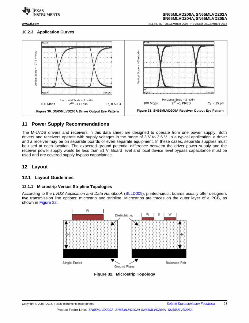
10.2.3 Application Curves
100 Mbps 215 –1 PRBS CL = 15 pF100 Mbps 215 –1 PRBS RL = 50 Ω
Figure 31. SN65MLVD200A Receiver Output Eye PatternFigure 30. SN65MLVD200A Driver Output Eye Pattern
11 Power Supply RecommendationsThe M-LVDS drivers and receivers in this data sheet are designed to operate from one power supply. Bothdrivers and receivers operate with supply voltages in the range of 3 V to 3.6 V. In a typical application, a driverand a receiver may be on separate boards or even separate equipment. In these cases, separate supplies mustbe used at each location. The expected ground potential difference between the driver power supply and thereceiver power supply would be less than ±1 V. Board level and local device level bypass capacitance must beused and are covered supply bypass capacitance.
12 Layout
12.1 Layout Guidelines
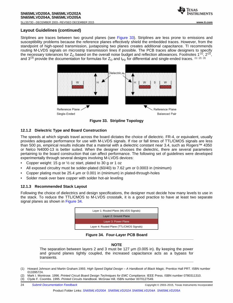
12.1.1 Microstrip Versus Stripline TopologiesAccording to the LVDS Application and Data Handbook (SLLD009), printed-circuit boards usually offer designerstwo transmission line options: microstrip and stripline. Microstrips are traces on the outer layer of a PCB, asshown in Figure 32.
Figure 32. Microstrip Topology
Copyright © 2003–2015, Texas Instruments Incorporated Submit Documentation Feedback 23
Product Folder Links: SN65MLVD200A SN65MLVD202A SN65MLVD204A SN65MLVD205A
Layer 4: Routed Plane (TTL/CMOS Signals)
Layer 3: Power Plane
Layer 2: Ground Plane
Layer 1: Routed Plane (MLVDS Signals)
SN65MLVD200A, SN65MLVD202ASN65MLVD204A, SN65MLVD205ASLLS573D –DECEMBER 2003–REVISED DECEMBER 2015 www.ti.com
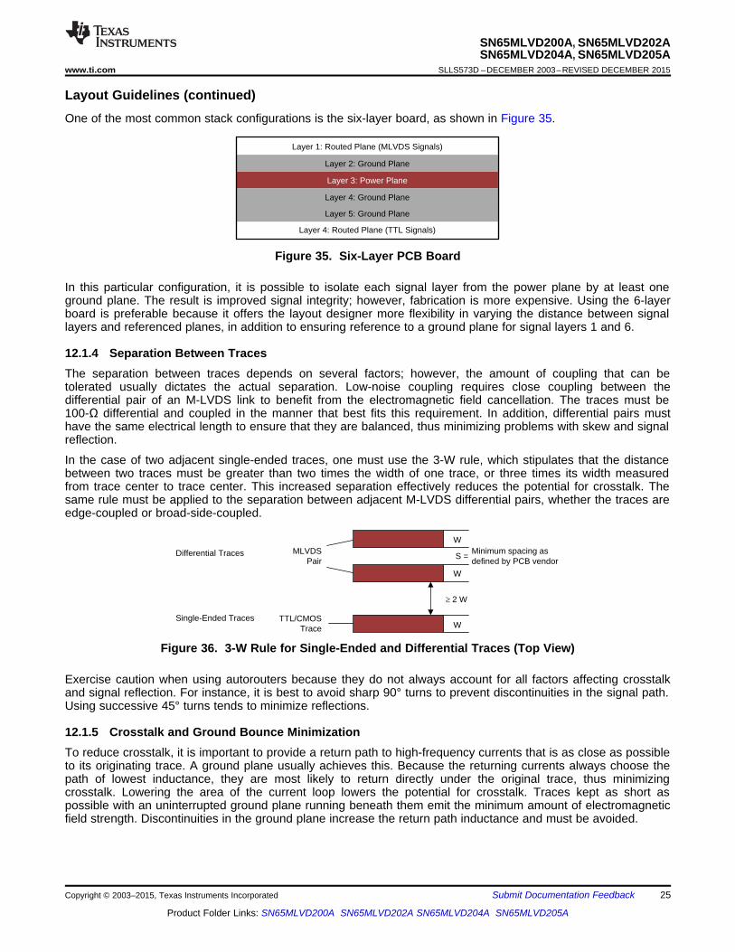
Layout Guidelines (continued)Striplines are traces between two ground planes (see Figure 33). Striplines are less prone to emissions andsusceptibility problems because the reference planes effectively shield the embedded traces. However, from thestandpoint of high-speed transmission, juxtaposing two planes creates additional capacitance. TI recommendsrouting M-LVDS signals on microstrip transmission lines if possible. The PCB traces allow designers to specifythe necessary tolerances for ZO based on the overall noise budget and reflection allowances. Footnotes 1 (1), 2 (2),and 3 (3) provide the documentation for formulas for ZO and tPD for differential and single-ended traces. (1) (2) (3)
Figure 33. Stripline Topology
12.1.2 Dielectric Type and Board ConstructionThe speeds at which signals travel across the board dictates the choice of dielectric. FR-4, or equivalent, usuallyprovides adequate performance for use with M-LVDS signals. If rise or fall times of TTL/CMOS signals are lessthan 500 ps, empirical results indicate that a material with a dielectric constant near 3.4, such as Rogers™ 4350or Nelco N4000-13 is better suited. When the designer chooses the dielectric, there are several parameterspertaining to the board construction that can affect performance. The following set of guidelines were developedexperimentally through several designs involving M-LVDS devices:• Copper weight: 15 g or ½ oz start, plated to 30 g or 1 oz• All exposed circuitry must be solder-plated (60/40) to 7.62 μm or 0.0003 in (minimum)• Copper plating must be 25.4 μm or 0.001 in (minimum) in plated-through-holes• Solder mask over bare copper with solder hot-air leveling
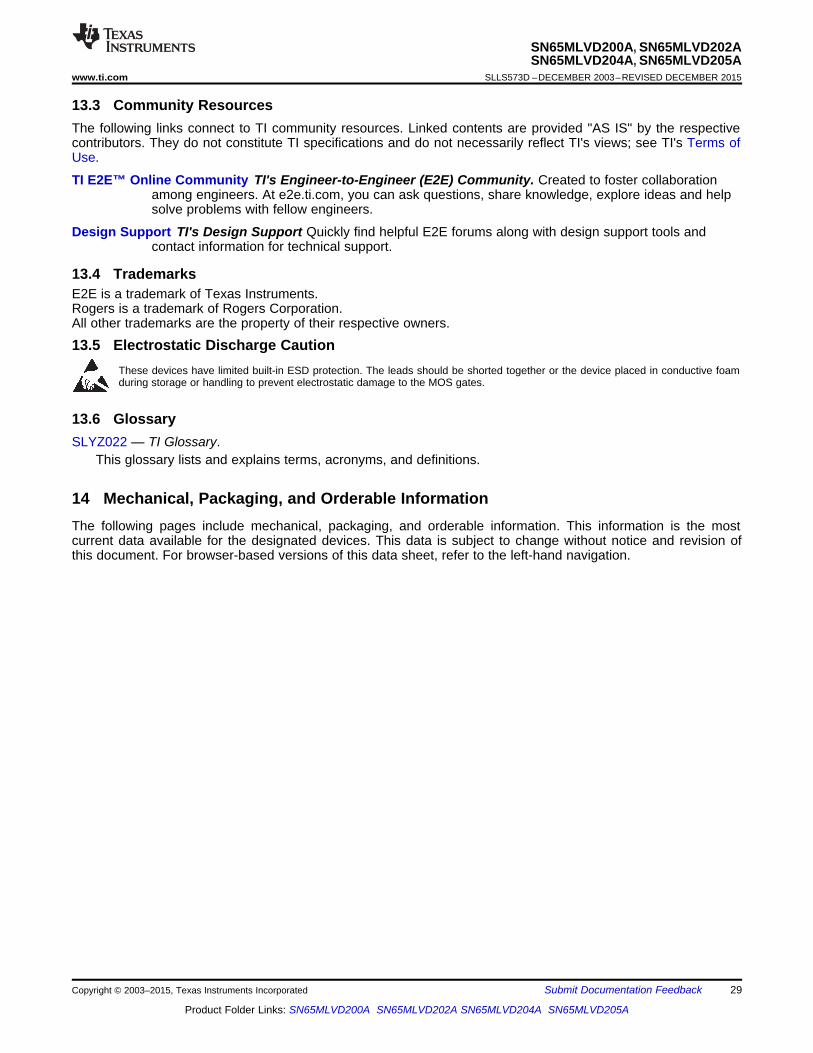
12.1.3 Recommended Stack LayoutFollowing the choice of dielectrics and design specifications, the designer must decide how many levels to use inthe stack. To reduce the TTL/CMOS to M-LVDS crosstalk, it is a good practice to have at least two separatesignal planes as shown in Figure 34.
Figure 34. Four-Layer PCB Board
NOTEThe separation between layers 2 and 3 must be 127 μm (0.005 in). By keeping the powerand ground planes tightly coupled, the increased capacitance acts as a bypass fortransients.
(1) Howard Johnson and Martin Graham.1993. High Speed Digital Design – A Handbook of Black Magic. Prentice Hall PRT. ISBN number013395724.
(2) Mark I. Montrose. 1996. Printed Circuit Board Design Techniques for EMC Compliance. IEEE Press. ISBN number 0780311310.(3) Clyde F. Coombs. 1995. Printed Circuits Handbook. McGraw Hill. ISBN number 0070127549.
24 Submit Documentation Feedback Copyright © 2003–2015, Texas Instruments Incorporated
Product Folder Links: SN65MLVD200A SN65MLVD202A SN65MLVD204A SN65MLVD205A
t2 W
W
W
W
Minimum spacing asdefined by PCB vendor
MLVDSPair
TTL/CMOSTrace
Differential Traces
Single-Ended Traces
S =
Layer 4: Routed Plane (TTL Signals)
Layer 3: Power Plane
Layer 2: Ground Plane
Layer 1: Routed Plane (MLVDS Signals)
Layer 4: Ground Plane
Layer 5: Ground Plane
SN65MLVD200A, SN65MLVD202ASN65MLVD204A, SN65MLVD205A
www.ti.com SLLS573D –DECEMBER 2003–REVISED DECEMBER 2015
Layout Guidelines (continued)One of the most common stack configurations is the six-layer board, as shown in Figure 35.
Figure 35. Six-Layer PCB Board
In this particular configuration, it is possible to isolate each signal layer from the power plane by at least oneground plane. The result is improved signal integrity; however, fabrication is more expensive. Using the 6-layerboard is preferable because it offers the layout designer more flexibility in varying the distance between signallayers and referenced planes, in addition to ensuring reference to a ground plane for signal layers 1 and 6.
12.1.4 Separation Between TracesThe separation between traces depends on several factors; however, the amount of coupling that can betolerated usually dictates the actual separation. Low-noise coupling requires close coupling between thedifferential pair of an M-LVDS link to benefit from the electromagnetic field cancellation. The traces must be100-Ω differential and coupled in the manner that best fits this requirement. In addition, differential pairs musthave the same electrical length to ensure that they are balanced, thus minimizing problems with skew and signalreflection.
In the case of two adjacent single-ended traces, one must use the 3-W rule, which stipulates that the distancebetween two traces must be greater than two times the width of one trace, or three times its width measuredfrom trace center to trace center. This increased separation effectively reduces the potential for crosstalk. Thesame rule must be applied to the separation between adjacent M-LVDS differential pairs, whether the traces areedge-coupled or broad-side-coupled.
Figure 36. 3-W Rule for Single-Ended and Differential Traces (Top View)
Exercise caution when using autorouters because they do not always account for all factors affecting crosstalkand signal reflection. For instance, it is best to avoid sharp 90° turns to prevent discontinuities in the signal path.Using successive 45° turns tends to minimize reflections.
12.1.5 Crosstalk and Ground Bounce MinimizationTo reduce crosstalk, it is important to provide a return path to high-frequency currents that is as close as possibleto its originating trace. A ground plane usually achieves this. Because the returning currents always choose thepath of lowest inductance, they are most likely to return directly under the original trace, thus minimizingcrosstalk. Lowering the area of the current loop lowers the potential for crosstalk. Traces kept as short aspossible with an uninterrupted ground plane running beneath them emit the minimum amount of electromagneticfield strength. Discontinuities in the ground plane increase the return path inductance and must be avoided.
Copyright © 2003–2015, Texas Instruments Incorporated Submit Documentation Feedback 25
Product Folder Links: SN65MLVD200A SN65MLVD202A SN65MLVD204A SN65MLVD205A

Boa
rd th
ickn
ess
appr
oxim
atel
y 10
0 m
il
2 mil
Typical 12-Layer PCB
4 mil
4 mil
6 mil
6 mil
VCCVia
GNDVia
TOP signal layer + GND fill
VDD 1 planeGND planeSignal layer
Buried capacitor>
Signal layerGND plane
VDD 2 planeBOTTOM signal layer + GND fill
Buried capacitor>
GND plane
Signal layers
VCC plane
SN65MLVD200A, SN65MLVD202ASN65MLVD204A, SN65MLVD205ASLLS573D –DECEMBER 2003–REVISED DECEMBER 2015 www.ti.com
Layout Guidelines (continued)12.1.6 DecouplingEach power or ground lead of a high-speed device must be connected to the PCB through a low inductancepath. For best results, one or more vias are used to connect a power or ground pin to the nearby plane. Ideally,via placement is immediately adjacent to the pin to avoid adding trace inductance. Placing a power plane closerto the top of the board reduces the effective via length and its associated inductance.
Figure 37. Low Inductance, High-Capacitance Power Connection
Bypass capacitors must be placed close to VDD pins and can be placed conveniently near the corners orunderneath the package to minimize the loop area. This extends the useful frequency range of the addedcapacitance. Small physical-size capacitors (such as 0402, 0201, or X7R surface-mount capacitors) must beused to minimize body inductance of capacitors. Each bypass capacitor is connected to the power and groundplane through vias tangent to the pads of the capacitor as shown in Figure 38(a).
An X7R surface-mount capacitor of size 0402 has about 0.5 nH of body inductance. At frequencies above about30 MHz, X7R capacitors behave as low-impedance inductors. To extend the operating frequency range to a fewhundred MHz, an array of different capacitor values like 100 pF, 1 nF, 0.03 μF, and 0.1 μF are commonly used inparallel. The most effective bypass capacitor can be built using sandwiched layers of power and ground at aseparation of 2 to 3 mils. With a 2-mil FR4 dielectric, there is approximately 500 pF per square inch of PCB.
Many high-speed devices provide a low-inductance GND connection on the backside of the package. This centerpad must be connected to a ground plane through an array of vias. The via array reduces the effectiveinductance to ground and enhances the thermal performance of the small surface mount technology (SMT)package. Placing vias around the perimeter of the pad connection ensures proper heat spreading and the lowestpossible die temperature. Placing high-performance devices on opposing sides of the PCB using two GNDplanes (as shown in Figure 29) creates multiple paths for heat transfer.
Thermal PCB issues are often the result of one device adding heat to another, resulting in a very high localtemperature. Multiple paths for heat transfer minimize this possibility. In many cases, the GND pad that is soimportant for heat dissipation makes the optimal decoupling layout impossible to achieve, due to insufficient pad-to-pad spacing as shown in Figure 39(b). When this occurs, placing the decoupling capacitor on the backside ofthe board keeps the extra inductance to a minimum.
26 Submit Documentation Feedback Copyright © 2003–2015, Texas Instruments Incorporated
Product Folder Links: SN65MLVD200A SN65MLVD202A SN65MLVD204A SN65MLVD205A

Layer 6
Layer 1
0402
VDD
IN±
IN+
0402
SN65MLVD200A, SN65MLVD202ASN65MLVD204A, SN65MLVD205A
www.ti.com SLLS573D –DECEMBER 2003–REVISED DECEMBER 2015
Layout Guidelines (continued)It is important to place the VDD via as close to the device pin as possible while still allowing for sufficient soldermask coverage. If the via is left open, solder may flow from the pad into the via barrel, which results in a poorsolder connection
Figure 38. Typical Decoupling Capacitor Layout (a)
Figure 39. Typical Decoupling Capacitor Layout (b)
12.2 Layout ExampleAt least two or three times the width of an individual trace must separate single-ended traces and differentialpairs to minimize the potential for crosstalk. Single-ended traces that run in parallel for less than the wavelengthof the rise or fall times usually have negligible crosstalk. Increase the spacing between signal paths for longparallel runs to reduce crosstalk. Boards with limited real estate can benefit from the staggered trace layout, asshown in Figure 40.
Figure 40. Staggered Trace Layout
This configuration lays out alternating signal traces on different layers; thus, the horizontal separation betweentraces can be less than 2 or 3 times the width of individual traces. To ensure continuity in the ground signal path,TI recommends having an adjacent ground via for every signal via, as shown in Figure 41.
NOTEVias create additional capacitance. For example, a typical via has a lumped capacitanceeffect of ½ pF to 1 pF in FR4.
Copyright © 2003–2015, Texas Instruments Incorporated Submit Documentation Feedback 27
Product Folder Links: SN65MLVD200A SN65MLVD202A SN65MLVD204A SN65MLVD205A

Signal Trace
Uninterrupted Ground Plane
Signal Trace
Uninterrupted Ground Plane
Signal Via
Ground Via
SN65MLVD200A, SN65MLVD202ASN65MLVD204A, SN65MLVD205ASLLS573D –DECEMBER 2003–REVISED DECEMBER 2015 www.ti.com
Layout Example (continued)
Figure 41. Ground Via Location (Side View)
Short and low-impedance connection of the device ground pins to the PCB ground plane reduces groundbounce. Holes and cutouts in the ground planes can adversely affect current return paths if they creatediscontinuities that increase returning current loop areas.
To minimize EMI problems, TI recommends avoiding discontinuities below a trace (for example, holes, slits, andso on) and keeping traces as short as possible. Zoning the board wisely by placing all similar functions in thesame area, as opposed to mixing them together, helps reduce susceptibility issues.
13 Device and Documentation Support
13.1 Documentation Support
13.1.1 Related DocumentationFor related documentation, see the following:• Introduction to M-LVDS (TIA/EIA-899) (SLLA108)• LVDS Application and Data Handbook (SLLD009)• LVDS Owner's Manual Design Guide, 4th Edition (SNLA187)• Semiconductor and IC Package Thermal Metrics (SPRA953)• Howard Johnson and Martin Graham.1993. High Speed Digital Design – A Handbook of Black Magic.
Prentice Hall PRT. ISBN number 013395724.• Mark I. Montrose. 1996. Printed Circuit Board Design Techniques for EMC Compliance. IEEE Press. ISBN
number 0780311310.• Clyde F. Coombs. 1995. Printed Circuits Handbook. McGraw Hill. ISBN number 0070127549.
13.2 Related LinksThe table below lists quick access links. Categories include technical documents, support and communityresources, tools and software, and quick access to sample or buy.
Table 8. Related LinksTECHNICAL TOOLS & SUPPORT &PARTS PRODUCT FOLDER SAMPLE & BUY DOCUMENTS SOFTWARE COMMUNITY
SN65MLVD200A Click here Click here Click here Click here Click hereSN65MLVD202A Click here Click here Click here Click here Click hereSN65MLVD204A Click here Click here Click here Click here Click hereSN65MLVD205A Click here Click here Click here Click here Click here
28 Submit Documentation Feedback Copyright © 2003–2015, Texas Instruments Incorporated
Product Folder Links: SN65MLVD200A SN65MLVD202A SN65MLVD204A SN65MLVD205A
SN65MLVD200A, SN65MLVD202ASN65MLVD204A, SN65MLVD205A
www.ti.com SLLS573D –DECEMBER 2003–REVISED DECEMBER 2015
13.3 Community ResourcesThe following links connect to TI community resources. Linked contents are provided "AS IS" by the respectivecontributors. They do not constitute TI specifications and do not necessarily reflect TI's views; see TI's Terms ofUse.
TI E2E™ Online Community TI's Engineer-to-Engineer (E2E) Community. Created to foster collaborationamong engineers. At e2e.ti.com, you can ask questions, share knowledge, explore ideas and helpsolve problems with fellow engineers.
Design Support TI's Design Support Quickly find helpful E2E forums along with design support tools andcontact information for technical support.
13.4 TrademarksE2E is a trademark of Texas Instruments.Rogers is a trademark of Rogers Corporation.All other trademarks are the property of their respective owners.
13.5 Electrostatic Discharge CautionThese devices have limited built-in ESD protection. The leads should be shorted together or the device placed in conductive foamduring storage or handling to prevent electrostatic damage to the MOS gates.
13.6 GlossarySLYZ022 — TI Glossary.
This glossary lists and explains terms, acronyms, and definitions.
14 Mechanical, Packaging, and Orderable InformationThe following pages include mechanical, packaging, and orderable information. This information is the mostcurrent data available for the designated devices. This data is subject to change without notice and revision ofthis document. For browser-based versions of this data sheet, refer to the left-hand navigation.
Copyright © 2003–2015, Texas Instruments Incorporated Submit Documentation Feedback 29
Product Folder Links: SN65MLVD200A SN65MLVD202A SN65MLVD204A SN65MLVD205A
PACKAGE OPTION ADDENDUM
www.ti.com 24-Aug-2018
Addendum-Page 1
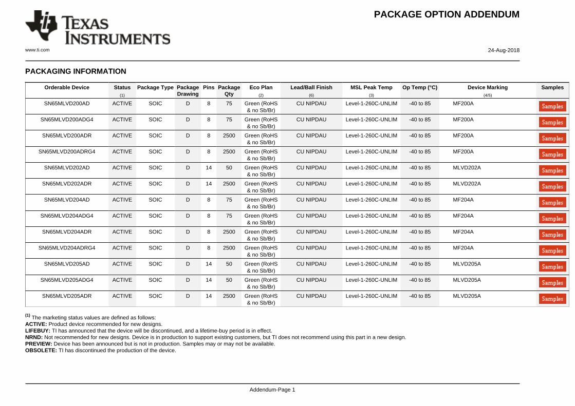
PACKAGING INFORMATION
Orderable Device Status(1)
Package Type PackageDrawing
Pins PackageQty
Eco Plan(2)
Lead/Ball Finish(6)
MSL Peak Temp(3)
Op Temp (°C) Device Marking(4/5)
Samples
SN65MLVD200AD ACTIVE SOIC D 8 75 Green (RoHS& no Sb/Br)
CU NIPDAU Level-1-260C-UNLIM -40 to 85 MF200A
SN65MLVD200ADG4 ACTIVE SOIC D 8 75 Green (RoHS& no Sb/Br)
CU NIPDAU Level-1-260C-UNLIM -40 to 85 MF200A
SN65MLVD200ADR ACTIVE SOIC D 8 2500 Green (RoHS& no Sb/Br)
CU NIPDAU Level-1-260C-UNLIM -40 to 85 MF200A
SN65MLVD200ADRG4 ACTIVE SOIC D 8 2500 Green (RoHS& no Sb/Br)
CU NIPDAU Level-1-260C-UNLIM -40 to 85 MF200A
SN65MLVD202AD ACTIVE SOIC D 14 50 Green (RoHS& no Sb/Br)
CU NIPDAU Level-1-260C-UNLIM -40 to 85 MLVD202A
SN65MLVD202ADR ACTIVE SOIC D 14 2500 Green (RoHS& no Sb/Br)
CU NIPDAU Level-1-260C-UNLIM -40 to 85 MLVD202A
SN65MLVD204AD ACTIVE SOIC D 8 75 Green (RoHS& no Sb/Br)
CU NIPDAU Level-1-260C-UNLIM -40 to 85 MF204A
SN65MLVD204ADG4 ACTIVE SOIC D 8 75 Green (RoHS& no Sb/Br)
CU NIPDAU Level-1-260C-UNLIM -40 to 85 MF204A
SN65MLVD204ADR ACTIVE SOIC D 8 2500 Green (RoHS& no Sb/Br)
CU NIPDAU Level-1-260C-UNLIM -40 to 85 MF204A
SN65MLVD204ADRG4 ACTIVE SOIC D 8 2500 Green (RoHS& no Sb/Br)
CU NIPDAU Level-1-260C-UNLIM -40 to 85 MF204A
SN65MLVD205AD ACTIVE SOIC D 14 50 Green (RoHS& no Sb/Br)
CU NIPDAU Level-1-260C-UNLIM -40 to 85 MLVD205A
SN65MLVD205ADG4 ACTIVE SOIC D 14 50 Green (RoHS& no Sb/Br)
CU NIPDAU Level-1-260C-UNLIM -40 to 85 MLVD205A
SN65MLVD205ADR ACTIVE SOIC D 14 2500 Green (RoHS& no Sb/Br)
CU NIPDAU Level-1-260C-UNLIM -40 to 85 MLVD205A
(1) The marketing status values are defined as follows:ACTIVE: Product device recommended for new designs.LIFEBUY: TI has announced that the device will be discontinued, and a lifetime-buy period is in effect.NRND: Not recommended for new designs. Device is in production to support existing customers, but TI does not recommend using this part in a new design.PREVIEW: Device has been announced but is not in production. Samples may or may not be available.OBSOLETE: TI has discontinued the production of the device.
PACKAGE OPTION ADDENDUM
www.ti.com 24-Aug-2018
Addendum-Page 2
(2) RoHS: TI defines "RoHS" to mean semiconductor products that are compliant with the current EU RoHS requirements for all 10 RoHS substances, including the requirement that RoHS substancedo not exceed 0.1% by weight in homogeneous materials. Where designed to be soldered at high temperatures, "RoHS" products are suitable for use in specified lead-free processes. TI mayreference these types of products as "Pb-Free".RoHS Exempt: TI defines "RoHS Exempt" to mean products that contain lead but are compliant with EU RoHS pursuant to a specific EU RoHS exemption.Green: TI defines "Green" to mean the content of Chlorine (Cl) and Bromine (Br) based flame retardants meet JS709B low halogen requirements of <=1000ppm threshold. Antimony trioxide basedflame retardants must also meet the <=1000ppm threshold requirement.
(3) MSL, Peak Temp. - The Moisture Sensitivity Level rating according to the JEDEC industry standard classifications, and peak solder temperature.
(4) There may be additional marking, which relates to the logo, the lot trace code information, or the environmental category on the device.
(5) Multiple Device Markings will be inside parentheses. Only one Device Marking contained in parentheses and separated by a "~" will appear on a device. If a line is indented then it is a continuationof the previous line and the two combined represent the entire Device Marking for that device.
(6) Lead/Ball Finish - Orderable Devices may have multiple material finish options. Finish options are separated by a vertical ruled line. Lead/Ball Finish values may wrap to two lines if the finishvalue exceeds the maximum column width.
Important Information and Disclaimer:The information provided on this page represents TI's knowledge and belief as of the date that it is provided. TI bases its knowledge and belief on informationprovided by third parties, and makes no representation or warranty as to the accuracy of such information. Efforts are underway to better integrate information from third parties. TI has taken andcontinues to take reasonable steps to provide representative and accurate information but may not have conducted destructive testing or chemical analysis on incoming materials and chemicals.TI and TI suppliers consider certain information to be proprietary, and thus CAS numbers and other limited information may not be available for release.
In no event shall TI's liability arising out of such information exceed the total purchase price of the TI part(s) at issue in this document sold by TI to Customer on an annual basis.

TAPE AND REEL INFORMATION
*All dimensions are nominal
Device PackageType
PackageDrawing
Pins SPQ ReelDiameter
(mm)
ReelWidth
W1 (mm)
A0(mm)
B0(mm)
K0(mm)
P1(mm)
W(mm)
Pin1Quadrant
SN65MLVD200ADR SOIC D 8 2500 330.0 12.4 6.4 5.2 2.1 8.0 12.0 Q1
SN65MLVD202ADR SOIC D 14 2500 330.0 16.4 6.5 9.0 2.1 8.0 16.0 Q1
SN65MLVD204ADR SOIC D 8 2500 330.0 12.4 6.4 5.2 2.1 8.0 12.0 Q1
SN65MLVD205ADR SOIC D 14 2500 330.0 16.4 6.5 9.0 2.1 8.0 16.0 Q1
PACKAGE MATERIALS INFORMATION
www.ti.com 28-Oct-2015
Pack Materials-Page 1

*All dimensions are nominal
Device Package Type Package Drawing Pins SPQ Length (mm) Width (mm) Height (mm)
SN65MLVD200ADR SOIC D 8 2500 340.5 338.1 20.6
SN65MLVD202ADR SOIC D 14 2500 333.2 345.9 28.6
SN65MLVD204ADR SOIC D 8 2500 340.5 338.1 20.6
SN65MLVD205ADR SOIC D 14 2500 333.2 345.9 28.6
PACKAGE MATERIALS INFORMATION
www.ti.com 28-Oct-2015
Pack Materials-Page 2


IMPORTANT NOTICE
Texas Instruments Incorporated (TI) reserves the right to make corrections, enhancements, improvements and other changes to itssemiconductor products and services per JESD46, latest issue, and to discontinue any product or service per JESD48, latest issue. Buyersshould obtain the latest relevant information before placing orders and should verify that such information is current and complete.TI’s published terms of sale for semiconductor products (http://www.ti.com/sc/docs/stdterms.htm) apply to the sale of packaged integratedcircuit products that TI has qualified and released to market. Additional terms may apply to the use or sale of other types of TI products andservices.Reproduction of significant portions of TI information in TI data sheets is permissible only if reproduction is without alteration and isaccompanied by all associated warranties, conditions, limitations, and notices. TI is not responsible or liable for such reproduceddocumentation. Information of third parties may be subject to additional restrictions. Resale of TI products or services with statementsdifferent from or beyond the parameters stated by TI for that product or service voids all express and any implied warranties for theassociated TI product or service and is an unfair and deceptive business practice. TI is not responsible or liable for any such statements.Buyers and others who are developing systems that incorporate TI products (collectively, “Designers”) understand and agree that Designersremain responsible for using their independent analysis, evaluation and judgment in designing their applications and that Designers havefull and exclusive responsibility to assure the safety of Designers' applications and compliance of their applications (and of all TI productsused in or for Designers’ applications) with all applicable regulations, laws and other applicable requirements. Designer represents that, withrespect to their applications, Designer has all the necessary expertise to create and implement safeguards that (1) anticipate dangerousconsequences of failures, (2) monitor failures and their consequences, and (3) lessen the likelihood of failures that might cause harm andtake appropriate actions. Designer agrees that prior to using or distributing any applications that include TI products, Designer willthoroughly test such applications and the functionality of such TI products as used in such applications.TI’s provision of technical, application or other design advice, quality characterization, reliability data or other services or information,including, but not limited to, reference designs and materials relating to evaluation modules, (collectively, “TI Resources”) are intended toassist designers who are developing applications that incorporate TI products; by downloading, accessing or using TI Resources in anyway, Designer (individually or, if Designer is acting on behalf of a company, Designer’s company) agrees to use any particular TI Resourcesolely for this purpose and subject to the terms of this Notice.TI’s provision of TI Resources does not expand or otherwise alter TI’s applicable published warranties or warranty disclaimers for TIproducts, and no additional obligations or liabilities arise from TI providing such TI Resources. TI reserves the right to make corrections,enhancements, improvements and other changes to its TI Resources. TI has not conducted any testing other than that specificallydescribed in the published documentation for a particular TI Resource.Designer is authorized to use, copy and modify any individual TI Resource only in connection with the development of applications thatinclude the TI product(s) identified in such TI Resource. NO OTHER LICENSE, EXPRESS OR IMPLIED, BY ESTOPPEL OR OTHERWISETO ANY OTHER TI INTELLECTUAL PROPERTY RIGHT, AND NO LICENSE TO ANY TECHNOLOGY OR INTELLECTUAL PROPERTYRIGHT OF TI OR ANY THIRD PARTY IS GRANTED HEREIN, including but not limited to any patent right, copyright, mask work right, orother intellectual property right relating to any combination, machine, or process in which TI products or services are used. Informationregarding or referencing third-party products or services does not constitute a license to use such products or services, or a warranty orendorsement thereof. Use of TI Resources may require a license from a third party under the patents or other intellectual property of thethird party, or a license from TI under the patents or other intellectual property of TI.TI RESOURCES ARE PROVIDED “AS IS” AND WITH ALL FAULTS. TI DISCLAIMS ALL OTHER WARRANTIES ORREPRESENTATIONS, EXPRESS OR IMPLIED, REGARDING RESOURCES OR USE THEREOF, INCLUDING BUT NOT LIMITED TOACCURACY OR COMPLETENESS, TITLE, ANY EPIDEMIC FAILURE WARRANTY AND ANY IMPLIED WARRANTIES OFMERCHANTABILITY, FITNESS FOR A PARTICULAR PURPOSE, AND NON-INFRINGEMENT OF ANY THIRD PARTY INTELLECTUALPROPERTY RIGHTS. TI SHALL NOT BE LIABLE FOR AND SHALL NOT DEFEND OR INDEMNIFY DESIGNER AGAINST ANY CLAIM,INCLUDING BUT NOT LIMITED TO ANY INFRINGEMENT CLAIM THAT RELATES TO OR IS BASED ON ANY COMBINATION OFPRODUCTS EVEN IF DESCRIBED IN TI RESOURCES OR OTHERWISE. IN NO EVENT SHALL TI BE LIABLE FOR ANY ACTUAL,DIRECT, SPECIAL, COLLATERAL, INDIRECT, PUNITIVE, INCIDENTAL, CONSEQUENTIAL OR EXEMPLARY DAMAGES INCONNECTION WITH OR ARISING OUT OF TI RESOURCES OR USE THEREOF, AND REGARDLESS OF WHETHER TI HAS BEENADVISED OF THE POSSIBILITY OF SUCH DAMAGES.Unless TI has explicitly designated an individual product as meeting the requirements of a particular industry standard (e.g., ISO/TS 16949and ISO 26262), TI is not responsible for any failure to meet such industry standard requirements.Where TI specifically promotes products as facilitating functional safety or as compliant with industry functional safety standards, suchproducts are intended to help enable customers to design and create their own applications that meet applicable functional safety standardsand requirements. Using products in an application does not by itself establish any safety features in the application. Designers mustensure compliance with safety-related requirements and standards applicable to their applications. Designer may not use any TI products inlife-critical medical equipment unless authorized officers of the parties have executed a special contract specifically governing such use.Life-critical medical equipment is medical equipment where failure of such equipment would cause serious bodily injury or death (e.g., lifesupport, pacemakers, defibrillators, heart pumps, neurostimulators, and implantables). Such equipment includes, without limitation, allmedical devices identified by the U.S. Food and Drug Administration as Class III devices and equivalent classifications outside the U.S.TI may expressly designate certain products as completing a particular qualification (e.g., Q100, Military Grade, or Enhanced Product).Designers agree that it has the necessary expertise to select the product with the appropriate qualification designation for their applicationsand that proper product selection is at Designers’ own risk. Designers are solely responsible for compliance with all legal and regulatoryrequirements in connection with such selection.Designer will fully indemnify TI and its representatives against any damages, costs, losses, and/or liabilities arising out of Designer’s non-compliance with the terms and provisions of this Notice.
Mailing Address: Texas Instruments, Post Office Box 655303, Dallas, Texas 75265Copyright © 2018, Texas Instruments Incorporated