DS90C032 LVDS Quad CMOS Differential Line … LVDS Quad CMOS Differential Line Receiver Check for...
18
DS90C032 www.ti.com SNLS094D – JUNE 1998 – REVISED APRIL 2013 DS90C032 LVDS Quad CMOS Differential Line Receiver Check for Samples: DS90C032 1FEATURES DESCRIPTION TheDS90C032 is a quad CMOS differential line 2• >155.5 Mbps (77.7 MHz) switching rates receiver designed for applications requiring ultra low • Accepts small swing (350 mV) differential power dissipation and high data rates. The device signal levels supports data rates in excess of 155.5 Mbps (77.7 • Ultra low power dissipation MHz) and uses Low Voltage Differential Signaling (LVDS) technology. • 600 ps maximum differential skew (5V, 25°C) TheDS90C032 accepts low voltage (350 mV) • 6.0 ns maximum propagation delay differential input signals and translates them to • Industrial operating temperature range CMOS (TTL compatible) output levels. The receiver • Military operating temperature range option supports a TRI-STATE function that may be used to • Available in surface mount packaging (SOIC) multiplex outputs. The receiver also supports OPEN, shorted, and terminated (100Ω) input Failsafe with and (LCCC) the addition of external failsafe biasing. Receiver • Pin compatible with DS26C32A, MB570 output will be HIGH for both Failsafe conditions. (PECL), and 41LF (PECL) TheDS90C032 and companion line driver • Supports OPEN input fail-safe (DS90C031) provide a new alternative to high power • Supports short and terminated input fail-safe pseudo-ECL devices for high speed point-to-point with the addition of external failsafe biasing interface applications. • Compatible with IEEE 1596.3 SCI LVDS standard • Conforms to ANSI/TIA/EIA-644 LVDS standard • Available to Standard Microcircuit Drawing (SMD) 5962-95834 Connection Diagram Dual-In-Line Figure 1. See Package Number D (R-PDSO-G16) 1 Please be aware that an important notice concerning availability, standard warranty, and use in critical applications of Texas Instruments semiconductor products and disclaimers thereto appears at the end of this data sheet. 2All trademarks are the property of their respective owners. PRODUCTION DATA information is current as of publication date. Copyright © 1998–2013, Texas Instruments Incorporated Products conform to specifications per the terms of the Texas Instruments standard warranty. Production processing does not necessarily include testing of all parameters.
Transcript of DS90C032 LVDS Quad CMOS Differential Line … LVDS Quad CMOS Differential Line Receiver Check for...

DS90C032
www.ti.com SNLS094D –JUNE 1998–REVISED APRIL 2013
DS90C032 LVDS Quad CMOS Differential Line ReceiverCheck for Samples: DS90C032
1FEATURES DESCRIPTIONTheDS90C032 is a quad CMOS differential line
2• >155.5 Mbps (77.7 MHz) switching ratesreceiver designed for applications requiring ultra low
• Accepts small swing (350 mV) differential power dissipation and high data rates. The devicesignal levels supports data rates in excess of 155.5 Mbps (77.7
• Ultra low power dissipation MHz) and uses Low Voltage Differential Signaling(LVDS) technology.• 600 ps maximum differential skew (5V, 25°C)TheDS90C032 accepts low voltage (350 mV)• 6.0 ns maximum propagation delaydifferential input signals and translates them to• Industrial operating temperature rangeCMOS (TTL compatible) output levels. The receiver
• Military operating temperature range option supports a TRI-STATE function that may be used to• Available in surface mount packaging (SOIC) multiplex outputs. The receiver also supports OPEN,
shorted, and terminated (100Ω) input Failsafe withand (LCCC)the addition of external failsafe biasing. Receiver• Pin compatible with DS26C32A, MB570output will be HIGH for both Failsafe conditions.(PECL), and 41LF (PECL)TheDS90C032 and companion line driver• Supports OPEN input fail-safe(DS90C031) provide a new alternative to high power• Supports short and terminated input fail-safe pseudo-ECL devices for high speed point-to-point
with the addition of external failsafe biasing interface applications.• Compatible with IEEE 1596.3 SCI LVDS
standard• Conforms to ANSI/TIA/EIA-644 LVDS standard• Available to Standard Microcircuit Drawing
(SMD) 5962-95834
Connection Diagram
Dual-In-Line
Figure 1. See Package Number D (R-PDSO-G16)
1
Please be aware that an important notice concerning availability, standard warranty, and use in critical applications ofTexas Instruments semiconductor products and disclaimers thereto appears at the end of this data sheet.
2All trademarks are the property of their respective owners.
PRODUCTION DATA information is current as of publication date. Copyright © 1998–2013, Texas Instruments IncorporatedProducts conform to specifications per the terms of the TexasInstruments standard warranty. Production processing does notnecessarily include testing of all parameters.

DS90C032
SNLS094D –JUNE 1998–REVISED APRIL 2013 www.ti.com
Functional Diagram and Truth Table
Receiver
ENABLES INPUTS OUTPUT
EN EN* RIN+ − RIN− ROUT
L H X Z
VID ≥ 0.1V H
VID ≤ −0.1V LAll other combinations ofFull Fail-safeENABLE inputs
OPEN/SHORT or HTerminated
2 Submit Documentation Feedback Copyright © 1998–2013, Texas Instruments Incorporated
Product Folder Links: DS90C032
DS90C032
www.ti.com SNLS094D –JUNE 1998–REVISED APRIL 2013
These devices have limited built-in ESD protection. The leads should be shorted together or the device placed in conductive foamduring storage or handling to prevent electrostatic damage to the MOS gates.
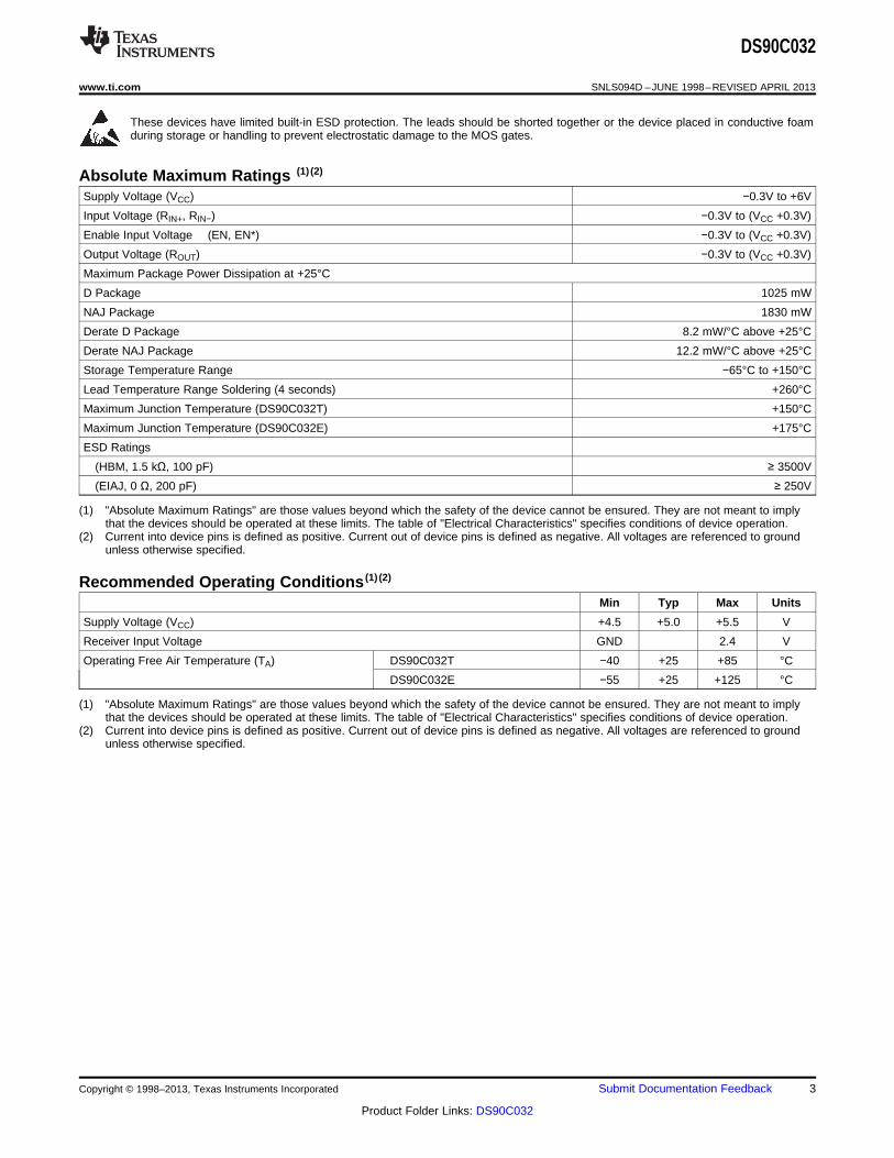
Absolute Maximum Ratings (1) (2)
Supply Voltage (VCC) −0.3V to +6V
Input Voltage (RIN+, RIN−) −0.3V to (VCC +0.3V)
Enable Input Voltage (EN, EN*) −0.3V to (VCC +0.3V)
Output Voltage (ROUT) −0.3V to (VCC +0.3V)
Maximum Package Power Dissipation at +25°C
D Package 1025 mW
NAJ Package 1830 mW
Derate D Package 8.2 mW/°C above +25°C
Derate NAJ Package 12.2 mW/°C above +25°C
Storage Temperature Range −65°C to +150°C
Lead Temperature Range Soldering (4 seconds) +260°C
Maximum Junction Temperature (DS90C032T) +150°C
Maximum Junction Temperature (DS90C032E) +175°C
ESD Ratings
(HBM, 1.5 kΩ, 100 pF) ≥ 3500V
(EIAJ, 0 Ω, 200 pF) ≥ 250V
(1) "Absolute Maximum Ratings" are those values beyond which the safety of the device cannot be ensured. They are not meant to implythat the devices should be operated at these limits. The table of "Electrical Characteristics" specifies conditions of device operation.
(2) Current into device pins is defined as positive. Current out of device pins is defined as negative. All voltages are referenced to groundunless otherwise specified.
Recommended Operating Conditions (1) (2)
Min Typ Max Units
Supply Voltage (VCC) +4.5 +5.0 +5.5 V
Receiver Input Voltage GND 2.4 V
Operating Free Air Temperature (TA) DS90C032T −40 +25 +85 °C
DS90C032E −55 +25 +125 °C
(1) "Absolute Maximum Ratings" are those values beyond which the safety of the device cannot be ensured. They are not meant to implythat the devices should be operated at these limits. The table of "Electrical Characteristics" specifies conditions of device operation.
(2) Current into device pins is defined as positive. Current out of device pins is defined as negative. All voltages are referenced to groundunless otherwise specified.
Copyright © 1998–2013, Texas Instruments Incorporated Submit Documentation Feedback 3
Product Folder Links: DS90C032
DS90C032
SNLS094D –JUNE 1998–REVISED APRIL 2013 www.ti.com
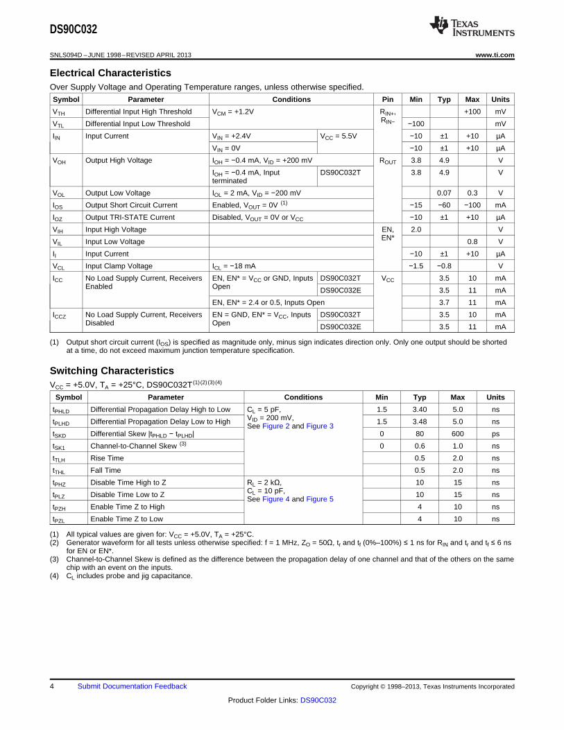
Electrical CharacteristicsOver Supply Voltage and Operating Temperature ranges, unless otherwise specified.
Symbol Parameter Conditions Pin Min Typ Max Units
VTH Differential Input High Threshold VCM = +1.2V RIN+, +100 mVRIN−VTL Differential Input Low Threshold −100 mV
IIN Input Current VIN = +2.4V VCC = 5.5V −10 ±1 +10 µA
VIN = 0V −10 ±1 +10 µA
VOH Output High Voltage IOH = −0.4 mA, VID = +200 mV ROUT 3.8 4.9 V
IOH = −0.4 mA, Input DS90C032T 3.8 4.9 Vterminated
VOL Output Low Voltage IOL = 2 mA, VID = −200 mV 0.07 0.3 V
IOS Output Short Circuit Current Enabled, VOUT = 0V (1) −15 −60 −100 mA
IOZ Output TRI-STATE Current Disabled, VOUT = 0V or VCC −10 ±1 +10 µA
VIH Input High Voltage EN, 2.0 VEN*VIL Input Low Voltage 0.8 V
II Input Current −10 ±1 +10 µA
VCL Input Clamp Voltage ICL = −18 mA −1.5 −0.8 V
ICC No Load Supply Current, Receivers EN, EN* = VCC or GND, Inputs DS90C032T VCC 3.5 10 mAEnabled Open DS90C032E 3.5 11 mA
EN, EN* = 2.4 or 0.5, Inputs Open 3.7 11 mA
ICCZ No Load Supply Current, Receivers EN = GND, EN* = VCC, Inputs DS90C032T 3.5 10 mADisabled Open DS90C032E 3.5 11 mA
(1) Output short circuit current (IOS) is specified as magnitude only, minus sign indicates direction only. Only one output should be shortedat a time, do not exceed maximum junction temperature specification.
Switching CharacteristicsVCC = +5.0V, TA = +25°C, DS90C032T (1) (2) (3) (4)
Symbol Parameter Conditions Min Typ Max Units
tPHLD Differential Propagation Delay High to Low CL = 5 pF, 1.5 3.40 5.0 nsVID = 200 mV,tPLHD Differential Propagation Delay Low to High 1.5 3.48 5.0 nsSee Figure 2 and Figure 3
tSKD Differential Skew |tPHLD − tPLHD| 0 80 600 ps
tSK1 Channel-to-Channel Skew (3) 0 0.6 1.0 ns
tTLH Rise Time 0.5 2.0 ns
tTHL Fall Time 0.5 2.0 ns
tPHZ Disable Time High to Z RL = 2 kΩ, 10 15 nsCL = 10 pF,tPLZ Disable Time Low to Z 10 15 nsSee Figure 4 and Figure 5
tPZH Enable Time Z to High 4 10 ns
tPZL Enable Time Z to Low 4 10 ns
(1) All typical values are given for: VCC = +5.0V, TA = +25°C.(2) Generator waveform for all tests unless otherwise specified: f = 1 MHz, ZO = 50Ω, tr and tf (0%–100%) ≤ 1 ns for RIN and tr and tf ≤ 6 ns
for EN or EN*.(3) Channel-to-Channel Skew is defined as the difference between the propagation delay of one channel and that of the others on the same
chip with an event on the inputs.(4) CL includes probe and jig capacitance.
4 Submit Documentation Feedback Copyright © 1998–2013, Texas Instruments Incorporated
Product Folder Links: DS90C032
DS90C032
www.ti.com SNLS094D –JUNE 1998–REVISED APRIL 2013
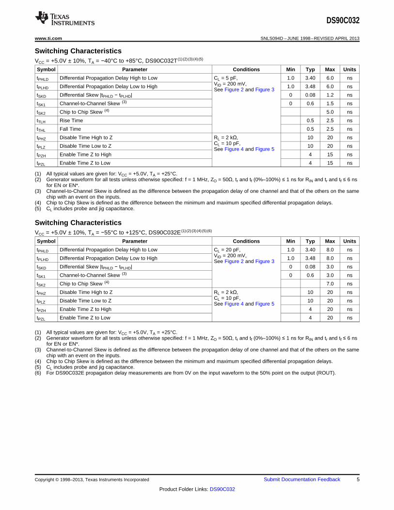
Switching CharacteristicsVCC = +5.0V ± 10%, TA = −40°C to +85°C, DS90C032T (1) (2) (3) (4) (5)
Symbol Parameter Conditions Min Typ Max Units
tPHLD Differential Propagation Delay High to Low CL = 5 pF, 1.0 3.40 6.0 nsVID = 200 mV,tPLHD Differential Propagation Delay Low to High 1.0 3.48 6.0 nsSee Figure 2 and Figure 3
tSKD Differential Skew |tPHLD − tPLHD| 0 0.08 1.2 ns
tSK1 Channel-to-Channel Skew (3) 0 0.6 1.5 ns
tSK2 Chip to Chip Skew (4) 5.0 ns
tTLH Rise Time 0.5 2.5 ns
tTHL Fall Time 0.5 2.5 ns
tPHZ Disable Time High to Z RL = 2 kΩ, 10 20 nsCL = 10 pF,tPLZ Disable Time Low to Z 10 20 nsSee Figure 4 and Figure 5
tPZH Enable Time Z to High 4 15 ns
tPZL Enable Time Z to Low 4 15 ns
(1) All typical values are given for: VCC = +5.0V, TA = +25°C.(2) Generator waveform for all tests unless otherwise specified: f = 1 MHz, ZO = 50Ω, tr and tf (0%–100%) ≤ 1 ns for RIN and tr and tf ≤ 6 ns
for EN or EN*.(3) Channel-to-Channel Skew is defined as the difference between the propagation delay of one channel and that of the others on the same
chip with an event on the inputs.(4) Chip to Chip Skew is defined as the difference between the minimum and maximum specified differential propagation delays.(5) CL includes probe and jig capacitance.
Switching CharacteristicsVCC = +5.0V ± 10%, TA = −55°C to +125°C, DS90C032E (1) (2) (3) (4) (5) (6)
Symbol Parameter Conditions Min Typ Max Units
tPHLD Differential Propagation Delay High to Low CL = 20 pF, 1.0 3.40 8.0 nsVID = 200 mV,tPLHD Differential Propagation Delay Low to High 1.0 3.48 8.0 nsSee Figure 2 and Figure 3
tSKD Differential Skew |tPHLD − tPLHD| 0 0.08 3.0 ns
tSK1 Channel-to-Channel Skew (3) 0 0.6 3.0 ns
tSK2 Chip to Chip Skew (4) 7.0 ns
tPHZ Disable Time High to Z RL = 2 kΩ, 10 20 nsCL = 10 pF,tPLZ Disable Time Low to Z 10 20 nsSee Figure 4 and Figure 5
tPZH Enable Time Z to High 4 20 ns
tPZL Enable Time Z to Low 4 20 ns
(1) All typical values are given for: VCC = +5.0V, TA = +25°C.(2) Generator waveform for all tests unless otherwise specified: f = 1 MHz, ZO = 50Ω, tr and tf (0%–100%) ≤ 1 ns for RIN and tr and tf ≤ 6 ns
for EN or EN*.(3) Channel-to-Channel Skew is defined as the difference between the propagation delay of one channel and that of the others on the same
chip with an event on the inputs.(4) Chip to Chip Skew is defined as the difference between the minimum and maximum specified differential propagation delays.(5) CL includes probe and jig capacitance.(6) For DS90C032E propagation delay measurements are from 0V on the input waveform to the 50% point on the output (ROUT).
Copyright © 1998–2013, Texas Instruments Incorporated Submit Documentation Feedback 5
Product Folder Links: DS90C032
DS90C032
SNLS094D –JUNE 1998–REVISED APRIL 2013 www.ti.com
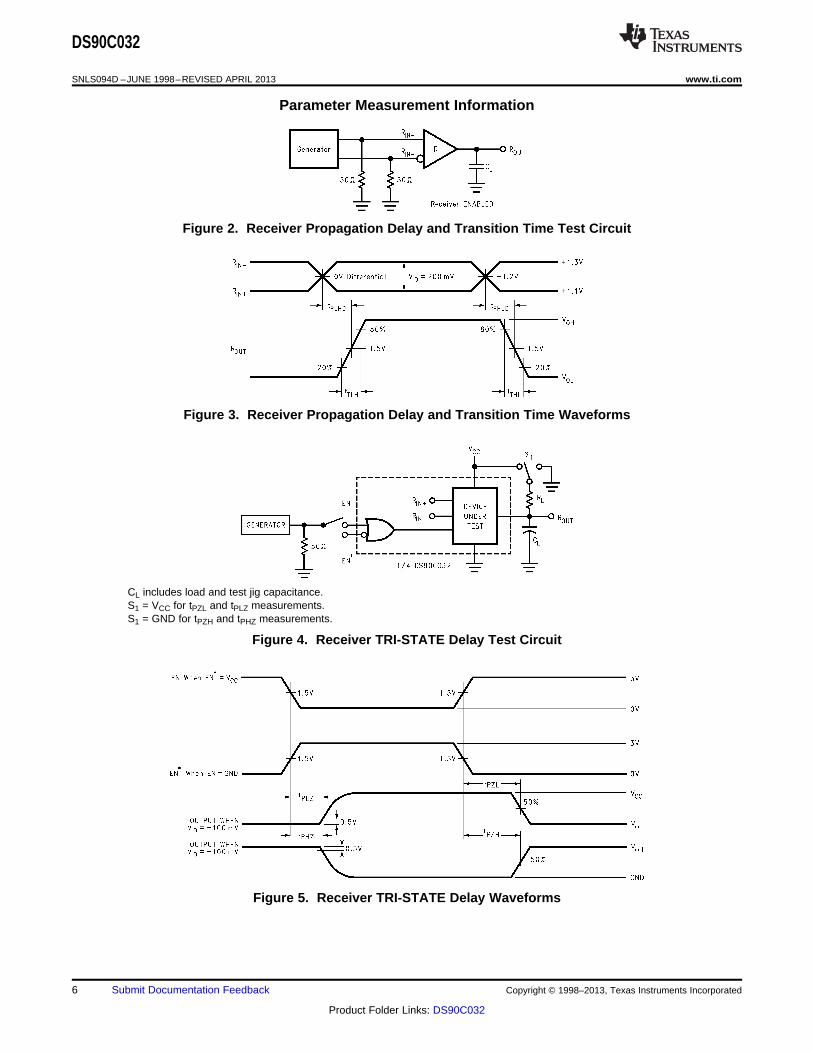
Parameter Measurement Information
Figure 2. Receiver Propagation Delay and Transition Time Test Circuit
Figure 3. Receiver Propagation Delay and Transition Time Waveforms
CL includes load and test jig capacitance.S1 = VCC for tPZL and tPLZ measurements.S1 = GND for tPZH and tPHZ measurements.
Figure 4. Receiver TRI-STATE Delay Test Circuit
Figure 5. Receiver TRI-STATE Delay Waveforms
6 Submit Documentation Feedback Copyright © 1998–2013, Texas Instruments Incorporated
Product Folder Links: DS90C032

DS90C032
www.ti.com SNLS094D –JUNE 1998–REVISED APRIL 2013
TYPICAL APPLICATION
Figure 6. Point-to-Point Application
APPLICATIONS INFORMATION
LVDS drivers and receivers are intended to be primarily used in an uncomplicated point-to-point configuration asis shown in Figure 6. This configuration provides a clean signaling environment for the quick edge rates of thedrivers. The receiver is connected to the driver through a balanced media which may be a standard twisted paircable, a parallel pair cable, or simply PCB traces. Typically the characteristic impedance of the media is in therange of 100Ω. A termination resistor of 100Ω should be selected to match the media, and is located as close tothe receiver input pins as possible. The termination resistor converts the current sourced by the driver into avoltage that is detected by the receiver. Other configurations are possible such as a multi-receiver configuration,but the effects of mid-stream connectors, cable stubs, and other impedance discontinuities as well as groundshifting, noise margin limits, and total termination loading must be taken into account.
The DS90C032 differential line receiver is capable of detecting signals as low as 100 mV, over a ±1V common-mode range centered around +1.2V. This is related to the driver offset voltage which is typically +1.2V. Thedriven signal is centered around this voltage and may shift ±1V around this center point. The ±1V shifting may bethe result of a ground potential difference between the driver's ground reference and the receiver's groundreference, the common-mode effects of coupled noise, or a combination of the two. Both receiver input pinsshould honor their specified operating input voltage range of 0V to +2.4V (measured from each pin to ground),exceeding these limits may turn on the ESD protection circuitry which will clamp the bus voltages.
Receiver Fail-Safe
The LVDS receiver is a high-gain high-speed device that amplifies a small differential signal (20mV) to CMOSlogic levels. Due to the high gain and tight threshold of the receiver, care should be taken to prevent noise fromappearing as a valid signal.
The receiver's internal fail-safe circuitry is designed to source or sink a small amount of current, providing fail-safe protection (a stable known state of HIGH output voltage) for floating, terminated, or shorted receiver inputs.1. Open Input Pins. TheDS90C032 is a quad receiver device, and if an application requires only 1, 2, or 3
receivers, the unused channel inputs should be left OPEN. Do not tie unused receiver inputs to ground orany other voltages. The input is biased by internal high-value pullup and pulldown resistors to set the outputto a HIGH state. This internal circuitry ensures a HIGH stable output state for open inputs.
2. Terminated Input. TheDS90C032 requires external failsafe biasing for terminated input failsafe.Terminated input failsafe is the case of a receiver that has a 100Ω termination across its inputs and thedriver is in the following situations. Unplugged from the bus, or the driver output is in TRI-STATE or in power-off condition. The use of external biasing resistors provide a small bias to set the differential input voltagewhile the line is un-driven, and therefore the receiver output will be in HIGH state. If the driver is removedfrom the bus but the cable is still present and floating, the unplugged cable can become a floating antennathat can pick up noise. The LVDS receiver is designed to detect very small amplitude and width signals andrecover them to standard logic levels. Thus, if the cable picks up more than 10mV of differential noise, thereceiver may respond. To insure that any noise is seen as common-mode and not differential, a balancedinterconnect and twisted pair cables is recommended, as they help to ensure that noise is coupled commonto both lines and rejected by the receivers.
3. Shorted Inputs. If a fault condition occurs that shorts the receiver inputs together, thus resulting in a 0Vdifferential input voltage, the receiver output will remain in a HIGH state. Shorted input fail-safe is notsupported across the common-mode range of the device (1.2V ±1V). It is only supported with inputs shortedand no external common-mode voltage applied.
4. Operation in environment with greater than 10mV differential noise.TI recommends external failsafe biasing on its LVDS receivers for a number of system level and signal
Copyright © 1998–2013, Texas Instruments Incorporated Submit Documentation Feedback 7
Product Folder Links: DS90C032
DS90C032
SNLS094D –JUNE 1998–REVISED APRIL 2013 www.ti.com
quality reasons. First, only an application that requires failsafe biasing needs to employ it. Second, theamount of failsafe biasing is now an application design parameter and can be custom tailored for the specificapplication. In applications in low noise environments, they may choose to use a very small bias if any. Forapplications with less balanced interconnects and/or in high noise environments they may choose to boostfailsafe further. TIs LVDS Owner’s Manual provides detailed calculations for selecting the proper failsafebiasing resistors. Third, the common-mode voltage is biased by the resistors during the un-driven state. Thisis selected to be close to the nominal driver offset voltage (VOS). Thus when switching between driven andun-driven states, the common-mode modulation on the bus is held to a minimum.For additional Failsafe Biasing information, please refer to Application Note AN-1194 (SNLA051) for moredetail.
The footprint of the DS90C032 is the same as the industry standard 26LS32 Quad Differential (RS-422)Receiver.
Pin Descriptions
Pin No. (SOIC) Name Description
2, 6, 10, 14 RIN+ Non-inverting receiver input pin
1, 7, 9, 15 RIN− Inverting receiver input pin
3, 5, 11, 13 ROUT Receiver output pin
4 EN Active high enable pin, OR-ed with EN*
12 EN* Active low enable pin, OR-ed with EN
16 VCC Power supply pin, +5V ± 10%
8 GND Ground pin
8 Submit Documentation Feedback Copyright © 1998–2013, Texas Instruments Incorporated
Product Folder Links: DS90C032
200
0
100
±40 ±15 10 35 60 85
TA ± Ambient Temperature (°C)
VO
L ±
Out
put L
ow V
olta
ge (
mV
) VCC = 5VVID = ±200 mV
200
100
04.5 4.75 5 5.25 5.5
TA = 25°CVID = ±200 mV
VCC ± Power Supply Voltage (V)
VO
L ± O
utpu
t Low
Vol
tage
(m
V)
5.5
5
4.5±40 ±15 10 35 60 85
TA ± Ambient Temperature (°C)
VO
H ±
Out
put H
igh
Vol
tage
(V
) VCC = 5VVID = 200 mV
6
5
44.5 4.75 5 5.25 5.5
VCC ± Power Supply Voltage (V)
VO
H ±
Out
put H
igh
Vol
tage
(V
)
TA = 25 °CVID = 200 mV
DS90C032
www.ti.com SNLS094D –JUNE 1998–REVISED APRIL 2013
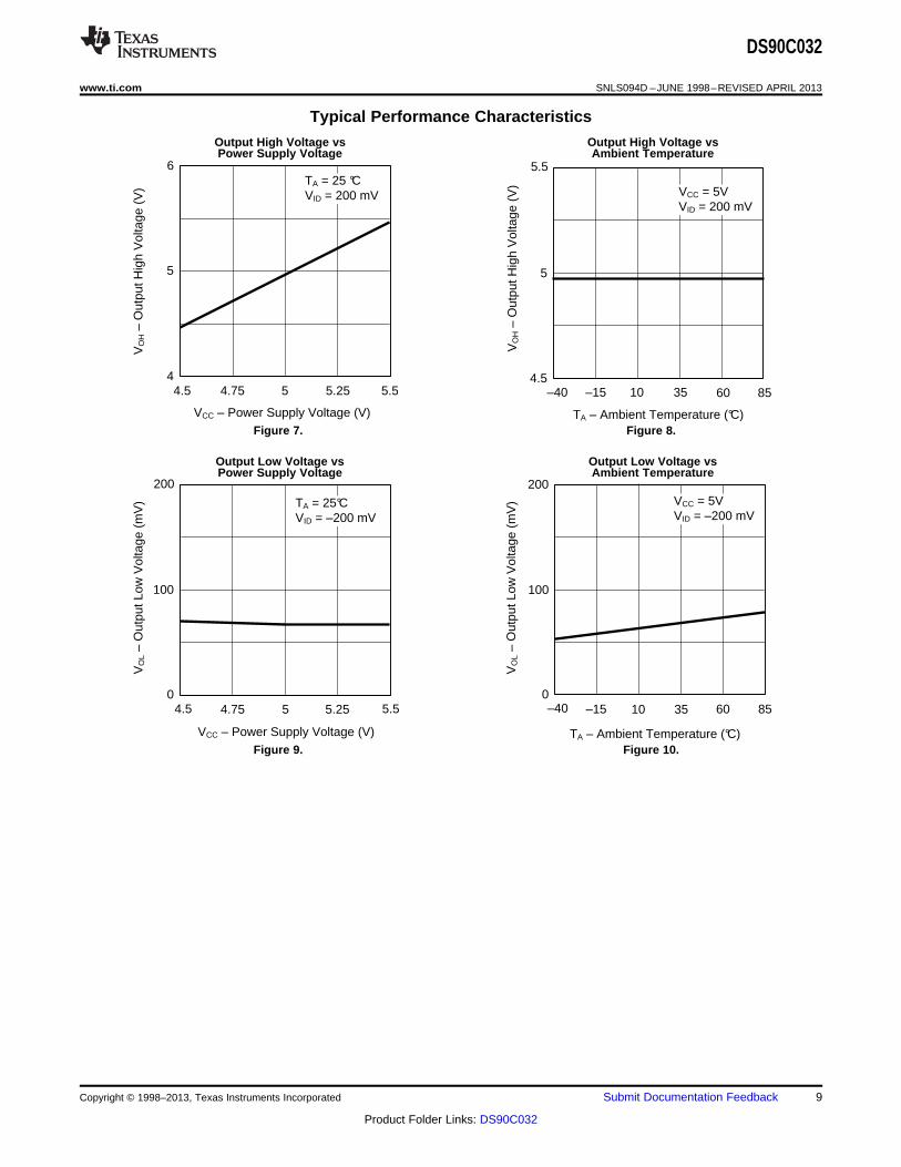
Typical Performance Characteristics
Output High Voltage vs Output High Voltage vsPower Supply Voltage Ambient Temperature
Figure 7. Figure 8.
Output Low Voltage vs Output Low Voltage vsPower Supply Voltage Ambient Temperature
Figure 9. Figure 10.
Copyright © 1998–2013, Texas Instruments Incorporated Submit Documentation Feedback 9
Product Folder Links: DS90C032
VCC = 5VFreq = 65 MHzVID = 200 mV CL = 5 pF
tPLHD
tPHLD
t PLH
D, t
PH
LD ±
Diff
eren
tial P
ropa
gatio
n D
elay
(ns
)
TA ± Ambient Temperature (°C)
5
4
3
2
1±40 ±15 10 35 60 85
VCC ± Power Supply Voltage (V)
TA = 25°CFreq = 65 MHzVID = 200 mV CL = 5 pF
4.754.5
tPLHD
tPHLD
5 5.25 5.5
5
4
3
2
1
t PLH
D, t
PH
LD ±
Diff
eren
tial P
ropa
gatio
n D
elay
(ns
)
TA = 25°CVOUT = 0V
±100
±80
±60
±40
±20
04.5 4.75 5 5.25 5.5
VCC ± Power Supply Voltage (V)
I OS ±
Out
put S
hort
Circ
uit C
urre
nt (
mA
)
VCC = 5VVOUT = 0V
TA ± Ambient Temperature (°C)
I OS ±
Out
put S
hort
Circ
uit C
urre
nt (
mA
) ±100
±80
±60
±40
±20
0±40 ±15 10 35 60 85
DS90C032
SNLS094D –JUNE 1998–REVISED APRIL 2013 www.ti.com
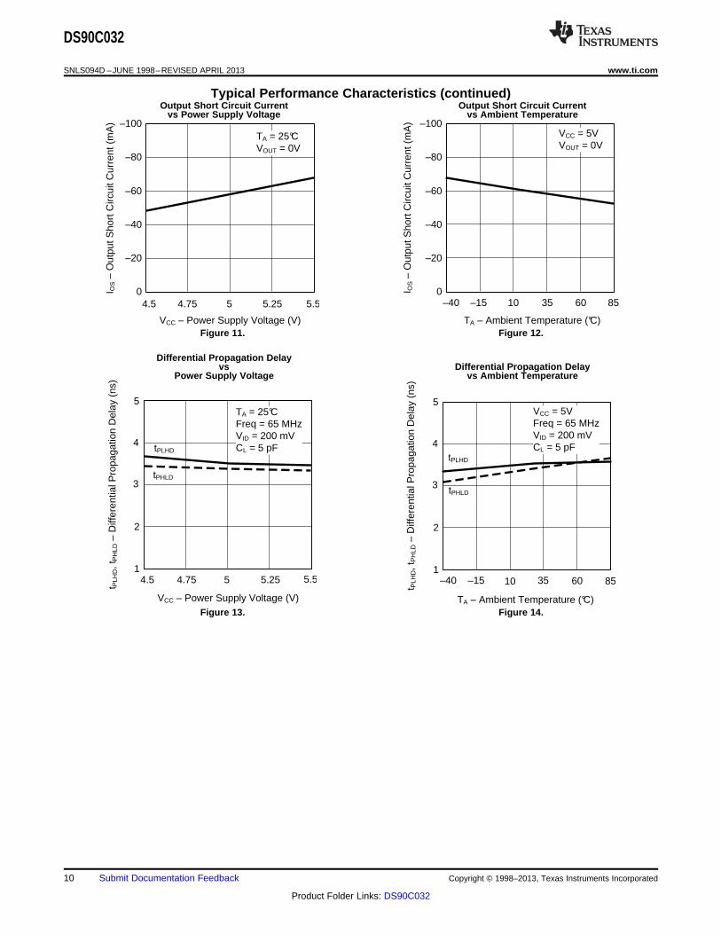
Typical Performance Characteristics (continued)Output Short Circuit Current Output Short Circuit Current
vs Power Supply Voltage vs Ambient Temperature
Figure 11. Figure 12.
Differential Propagation Delayvs Differential Propagation Delay
Power Supply Voltage vs Ambient Temperature
Figure 13. Figure 14.
10 Submit Documentation Feedback Copyright © 1998–2013, Texas Instruments Incorporated
Product Folder Links: DS90C032
TA = 25°CFreq = 65 MHz
tTLH
tTHL
VCC ± Power Supply Voltage (V)
t TLH
, tT
HL ± T
rans
ition
Tim
e (n
s)
1
0.8
0.6
0.4
0.2
04.5 4.75 5 5.25 5.5
tTLH
tTHL
TA ± Ambient Temperature (°C)
t TLH
, tT
HL ±
Tra
nsiti
on T
ime
(ns)
1
0.8
0.6
0.4
0.2
0
VCC = 5VFreq = 65 MHz
±40 ±15 10 35 60 85
TA = 25°CFreq = 65 MHzVID = 200 mV CL = 5 pF
VCC ± Power Supply Voltage (V)
t SK
D ±
Diff
eren
tial S
kew
(ns
)
1
0.8
0.6
0.4
0.2
04.5 4.75 5 5.25 5.5
VCC = 5VFreq = 65 MHzVID = 200 mV CL = 5 pF
t SK
D ±
Diff
eren
tial S
kew
(ns
)
1
0.8
0.6
0.4
0.2
0
TA ± Ambient Temperature (°C)
±40 ±15 10 35 60 85
DS90C032
www.ti.com SNLS094D –JUNE 1998–REVISED APRIL 2013
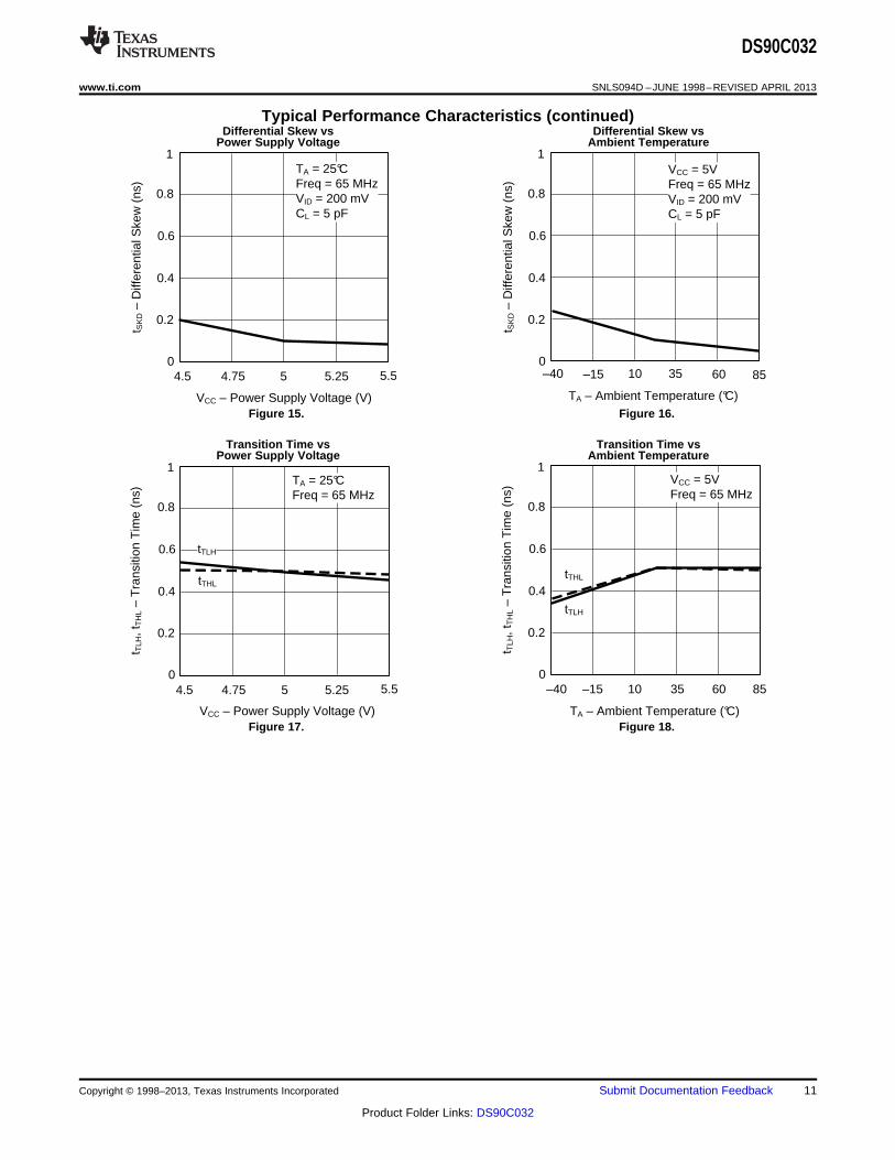
Typical Performance Characteristics (continued)Differential Skew vs Differential Skew vs
Power Supply Voltage Ambient Temperature
Figure 15. Figure 16.
Transition Time vs Transition Time vsPower Supply Voltage Ambient Temperature
Figure 17. Figure 18.
Copyright © 1998–2013, Texas Instruments Incorporated Submit Documentation Feedback 11
Product Folder Links: DS90C032
DS90C032
SNLS094D –JUNE 1998–REVISED APRIL 2013 www.ti.com
REVISION HISTORY
Changes from Revision C (April 2013) to Revision D Page
• Changed layout of National Data Sheet to TI format .......................................................................................................... 11
12 Submit Documentation Feedback Copyright © 1998–2013, Texas Instruments Incorporated
Product Folder Links: DS90C032
PACKAGE OPTION ADDENDUM
www.ti.com 25-Apr-2017
Addendum-Page 1
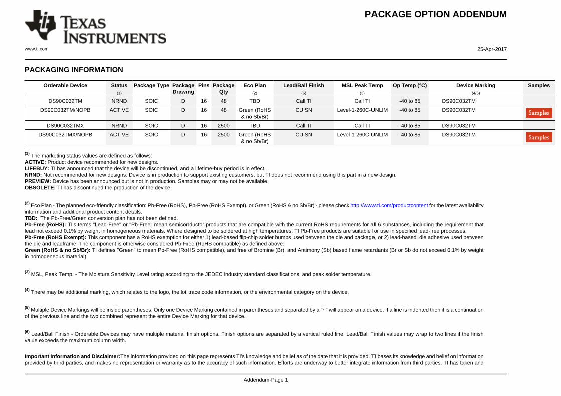
PACKAGING INFORMATION
Orderable Device Status(1)
Package Type PackageDrawing
Pins PackageQty
Eco Plan(2)
Lead/Ball Finish(6)
MSL Peak Temp(3)
Op Temp (°C) Device Marking(4/5)
Samples
DS90C032TM NRND SOIC D 16 48 TBD Call TI Call TI -40 to 85 DS90C032TM
DS90C032TM/NOPB ACTIVE SOIC D 16 48 Green (RoHS& no Sb/Br)
CU SN Level-1-260C-UNLIM -40 to 85 DS90C032TM
DS90C032TMX NRND SOIC D 16 2500 TBD Call TI Call TI -40 to 85 DS90C032TM
DS90C032TMX/NOPB ACTIVE SOIC D 16 2500 Green (RoHS& no Sb/Br)
CU SN Level-1-260C-UNLIM -40 to 85 DS90C032TM
(1) The marketing status values are defined as follows:ACTIVE: Product device recommended for new designs.LIFEBUY: TI has announced that the device will be discontinued, and a lifetime-buy period is in effect.NRND: Not recommended for new designs. Device is in production to support existing customers, but TI does not recommend using this part in a new design.PREVIEW: Device has been announced but is not in production. Samples may or may not be available.OBSOLETE: TI has discontinued the production of the device.
(2) Eco Plan - The planned eco-friendly classification: Pb-Free (RoHS), Pb-Free (RoHS Exempt), or Green (RoHS & no Sb/Br) - please check http://www.ti.com/productcontent for the latest availabilityinformation and additional product content details.TBD: The Pb-Free/Green conversion plan has not been defined.Pb-Free (RoHS): TI's terms "Lead-Free" or "Pb-Free" mean semiconductor products that are compatible with the current RoHS requirements for all 6 substances, including the requirement thatlead not exceed 0.1% by weight in homogeneous materials. Where designed to be soldered at high temperatures, TI Pb-Free products are suitable for use in specified lead-free processes.Pb-Free (RoHS Exempt): This component has a RoHS exemption for either 1) lead-based flip-chip solder bumps used between the die and package, or 2) lead-based die adhesive used betweenthe die and leadframe. The component is otherwise considered Pb-Free (RoHS compatible) as defined above.Green (RoHS & no Sb/Br): TI defines "Green" to mean Pb-Free (RoHS compatible), and free of Bromine (Br) and Antimony (Sb) based flame retardants (Br or Sb do not exceed 0.1% by weightin homogeneous material)
(3) MSL, Peak Temp. - The Moisture Sensitivity Level rating according to the JEDEC industry standard classifications, and peak solder temperature.
(4) There may be additional marking, which relates to the logo, the lot trace code information, or the environmental category on the device.
(5) Multiple Device Markings will be inside parentheses. Only one Device Marking contained in parentheses and separated by a "~" will appear on a device. If a line is indented then it is a continuationof the previous line and the two combined represent the entire Device Marking for that device.
(6) Lead/Ball Finish - Orderable Devices may have multiple material finish options. Finish options are separated by a vertical ruled line. Lead/Ball Finish values may wrap to two lines if the finishvalue exceeds the maximum column width.
Important Information and Disclaimer:The information provided on this page represents TI's knowledge and belief as of the date that it is provided. TI bases its knowledge and belief on informationprovided by third parties, and makes no representation or warranty as to the accuracy of such information. Efforts are underway to better integrate information from third parties. TI has taken and

PACKAGE OPTION ADDENDUM
www.ti.com 25-Apr-2017
Addendum-Page 2
continues to take reasonable steps to provide representative and accurate information but may not have conducted destructive testing or chemical analysis on incoming materials and chemicals.TI and TI suppliers consider certain information to be proprietary, and thus CAS numbers and other limited information may not be available for release.
In no event shall TI's liability arising out of such information exceed the total purchase price of the TI part(s) at issue in this document sold by TI to Customer on an annual basis.
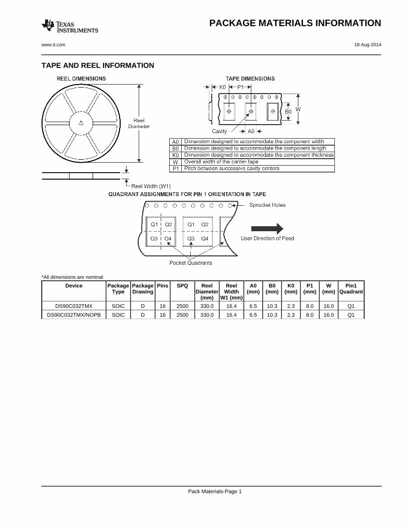
TAPE AND REEL INFORMATION
*All dimensions are nominal
Device PackageType
PackageDrawing
Pins SPQ ReelDiameter
(mm)
ReelWidth
W1 (mm)
A0(mm)
B0(mm)
K0(mm)
P1(mm)
W(mm)
Pin1Quadrant
DS90C032TMX SOIC D 16 2500 330.0 16.4 6.5 10.3 2.3 8.0 16.0 Q1
DS90C032TMX/NOPB SOIC D 16 2500 330.0 16.4 6.5 10.3 2.3 8.0 16.0 Q1
PACKAGE MATERIALS INFORMATION
www.ti.com 18-Aug-2014
Pack Materials-Page 1

*All dimensions are nominal
Device Package Type Package Drawing Pins SPQ Length (mm) Width (mm) Height (mm)
DS90C032TMX SOIC D 16 2500 367.0 367.0 35.0
DS90C032TMX/NOPB SOIC D 16 2500 367.0 367.0 35.0
PACKAGE MATERIALS INFORMATION
www.ti.com 18-Aug-2014
Pack Materials-Page 2


IMPORTANT NOTICE
Texas Instruments Incorporated (TI) reserves the right to make corrections, enhancements, improvements and other changes to itssemiconductor products and services per JESD46, latest issue, and to discontinue any product or service per JESD48, latest issue. Buyersshould obtain the latest relevant information before placing orders and should verify that such information is current and complete.TI’s published terms of sale for semiconductor products (http://www.ti.com/sc/docs/stdterms.htm) apply to the sale of packaged integratedcircuit products that TI has qualified and released to market. Additional terms may apply to the use or sale of other types of TI products andservices.Reproduction of significant portions of TI information in TI data sheets is permissible only if reproduction is without alteration and isaccompanied by all associated warranties, conditions, limitations, and notices. TI is not responsible or liable for such reproduceddocumentation. Information of third parties may be subject to additional restrictions. Resale of TI products or services with statementsdifferent from or beyond the parameters stated by TI for that product or service voids all express and any implied warranties for theassociated TI product or service and is an unfair and deceptive business practice. TI is not responsible or liable for any such statements.Buyers and others who are developing systems that incorporate TI products (collectively, “Designers”) understand and agree that Designersremain responsible for using their independent analysis, evaluation and judgment in designing their applications and that Designers havefull and exclusive responsibility to assure the safety of Designers' applications and compliance of their applications (and of all TI productsused in or for Designers’ applications) with all applicable regulations, laws and other applicable requirements. Designer represents that, withrespect to their applications, Designer has all the necessary expertise to create and implement safeguards that (1) anticipate dangerousconsequences of failures, (2) monitor failures and their consequences, and (3) lessen the likelihood of failures that might cause harm andtake appropriate actions. Designer agrees that prior to using or distributing any applications that include TI products, Designer willthoroughly test such applications and the functionality of such TI products as used in such applications.TI’s provision of technical, application or other design advice, quality characterization, reliability data or other services or information,including, but not limited to, reference designs and materials relating to evaluation modules, (collectively, “TI Resources”) are intended toassist designers who are developing applications that incorporate TI products; by downloading, accessing or using TI Resources in anyway, Designer (individually or, if Designer is acting on behalf of a company, Designer’s company) agrees to use any particular TI Resourcesolely for this purpose and subject to the terms of this Notice.TI’s provision of TI Resources does not expand or otherwise alter TI’s applicable published warranties or warranty disclaimers for TIproducts, and no additional obligations or liabilities arise from TI providing such TI Resources. TI reserves the right to make corrections,enhancements, improvements and other changes to its TI Resources. TI has not conducted any testing other than that specificallydescribed in the published documentation for a particular TI Resource.Designer is authorized to use, copy and modify any individual TI Resource only in connection with the development of applications thatinclude the TI product(s) identified in such TI Resource. NO OTHER LICENSE, EXPRESS OR IMPLIED, BY ESTOPPEL OR OTHERWISETO ANY OTHER TI INTELLECTUAL PROPERTY RIGHT, AND NO LICENSE TO ANY TECHNOLOGY OR INTELLECTUAL PROPERTYRIGHT OF TI OR ANY THIRD PARTY IS GRANTED HEREIN, including but not limited to any patent right, copyright, mask work right, orother intellectual property right relating to any combination, machine, or process in which TI products or services are used. Informationregarding or referencing third-party products or services does not constitute a license to use such products or services, or a warranty orendorsement thereof. Use of TI Resources may require a license from a third party under the patents or other intellectual property of thethird party, or a license from TI under the patents or other intellectual property of TI.TI RESOURCES ARE PROVIDED “AS IS” AND WITH ALL FAULTS. TI DISCLAIMS ALL OTHER WARRANTIES ORREPRESENTATIONS, EXPRESS OR IMPLIED, REGARDING RESOURCES OR USE THEREOF, INCLUDING BUT NOT LIMITED TOACCURACY OR COMPLETENESS, TITLE, ANY EPIDEMIC FAILURE WARRANTY AND ANY IMPLIED WARRANTIES OFMERCHANTABILITY, FITNESS FOR A PARTICULAR PURPOSE, AND NON-INFRINGEMENT OF ANY THIRD PARTY INTELLECTUALPROPERTY RIGHTS. TI SHALL NOT BE LIABLE FOR AND SHALL NOT DEFEND OR INDEMNIFY DESIGNER AGAINST ANY CLAIM,INCLUDING BUT NOT LIMITED TO ANY INFRINGEMENT CLAIM THAT RELATES TO OR IS BASED ON ANY COMBINATION OFPRODUCTS EVEN IF DESCRIBED IN TI RESOURCES OR OTHERWISE. IN NO EVENT SHALL TI BE LIABLE FOR ANY ACTUAL,DIRECT, SPECIAL, COLLATERAL, INDIRECT, PUNITIVE, INCIDENTAL, CONSEQUENTIAL OR EXEMPLARY DAMAGES INCONNECTION WITH OR ARISING OUT OF TI RESOURCES OR USE THEREOF, AND REGARDLESS OF WHETHER TI HAS BEENADVISED OF THE POSSIBILITY OF SUCH DAMAGES.Unless TI has explicitly designated an individual product as meeting the requirements of a particular industry standard (e.g., ISO/TS 16949and ISO 26262), TI is not responsible for any failure to meet such industry standard requirements.Where TI specifically promotes products as facilitating functional safety or as compliant with industry functional safety standards, suchproducts are intended to help enable customers to design and create their own applications that meet applicable functional safety standardsand requirements. Using products in an application does not by itself establish any safety features in the application. Designers mustensure compliance with safety-related requirements and standards applicable to their applications. Designer may not use any TI products inlife-critical medical equipment unless authorized officers of the parties have executed a special contract specifically governing such use.Life-critical medical equipment is medical equipment where failure of such equipment would cause serious bodily injury or death (e.g., lifesupport, pacemakers, defibrillators, heart pumps, neurostimulators, and implantables). Such equipment includes, without limitation, allmedical devices identified by the U.S. Food and Drug Administration as Class III devices and equivalent classifications outside the U.S.TI may expressly designate certain products as completing a particular qualification (e.g., Q100, Military Grade, or Enhanced Product).Designers agree that it has the necessary expertise to select the product with the appropriate qualification designation for their applicationsand that proper product selection is at Designers’ own risk. Designers are solely responsible for compliance with all legal and regulatoryrequirements in connection with such selection.Designer will fully indemnify TI and its representatives against any damages, costs, losses, and/or liabilities arising out of Designer’s non-compliance with the terms and provisions of this Notice.
Mailing Address: Texas Instruments, Post Office Box 655303, Dallas, Texas 75265Copyright © 2017, Texas Instruments Incorporated