DS90LV048A 3V LVDS Quad CMOS Differential Line Receiver … · 2016-09-12 · Product Folder Sample...
22
Product Folder Sample & Buy Technical Documents Tools & Software Support & Community An IMPORTANT NOTICE at the end of this data sheet addresses availability, warranty, changes, use in safety-critical applications, intellectual property matters and other important disclaimers. PRODUCTION DATA. DS90LV048A SNLS045C – JULY 1999 – REVISED JULY 2016 DS90LV048A 3-V LVDS Quad CMOS Differential Line Receiver 1 1 Features 1• > 400-Mbps (200-MHz) Switching Rates • Flow-Through Pinout Simplifies PCB Layout • 150-ps Channel-to-Channel Skew (Typical) • 100-ps Differential Skew (Typical) • 2.7-ns Maximum Propagation Delay • 3.3-V Power Supply Design • High Impedance LVDS Inputs on Power Down • Low Power Design (40 mW at 3.3-V Static) • Interoperable With Existing 5-V LVDS Drivers • Accepts Small Swing (350 mV Typical) Differential Signal Levels • Supports Input Failsafe – Open, Short, and Terminated • 0 V to −100 mV Threshold Region • Conforms to ANSI/TIA/EIA-644 Standard • Operating Temperature Range: –40°C to +85°C • Available in SOIC and TSSOP Package 2 Applications • Multifunction Printers • LVDS - LVCMOS Translation 3 Description The DS90LV048A device is a quad CMOS flow- through differential line receiver designed for applications requiring ultra-low power dissipation and high data rates. The device is designed to support data rates in excess of 400 Mbps (200 MHz) using Low Voltage Differential Signaling (LVDS) technology. The DS90LV048A accepts low voltage (350 mV typical) differential input signals and translates them to 3-V CMOS output levels. The receiver supports a TRI-STATE function that may be used to multiplex outputs. The receiver also supports open, shorted, and terminated (100-Ω) input fail-safe. The receiver output is HIGH for all fail-safe conditions. The DS90LV048A has a flow-through pinout for easy PCB layout. The EN and EN* inputs are ANDed together and control the TRI-STATE outputs. The enables are common to all four receivers. The DS90LV048A and companion LVDS line driver (for example, DS90LV047A) provide a new alternative to high- power PECL/ECL devices for high-speed point-to- point interface applications. Device Information (1) PART NUMBER PACKAGE BODY SIZE (NOM) DS90LV048A SOIC (16) 9.90 mm × 3.91 mm TSSOP (16) 5.00 mm × 4.40 mm (1) For all available packages, see the orderable addendum at the end of the data sheet. Functional Diagram
Transcript of DS90LV048A 3V LVDS Quad CMOS Differential Line Receiver … · 2016-09-12 · Product Folder Sample...
Product
Folder
Sample &Buy
Technical
Documents
Tools &
Software
Support &Community
An IMPORTANT NOTICE at the end of this data sheet addresses availability, warranty, changes, use in safety-critical applications,intellectual property matters and other important disclaimers. PRODUCTION DATA.
DS90LV048ASNLS045C –JULY 1999–REVISED JULY 2016
DS90LV048A 3-V LVDS Quad CMOS Differential Line Receiver
1
1 Features1• > 400-Mbps (200-MHz) Switching Rates• Flow-Through Pinout Simplifies PCB Layout• 150-ps Channel-to-Channel Skew (Typical)• 100-ps Differential Skew (Typical)• 2.7-ns Maximum Propagation Delay• 3.3-V Power Supply Design• High Impedance LVDS Inputs on Power Down• Low Power Design (40 mW at 3.3-V Static)• Interoperable With Existing 5-V LVDS Drivers• Accepts Small Swing (350 mV Typical) Differential
Signal Levels• Supports Input Failsafe
– Open, Short, and Terminated• 0 V to −100 mV Threshold Region• Conforms to ANSI/TIA/EIA-644 Standard• Operating Temperature Range: –40°C to +85°C• Available in SOIC and TSSOP Package
2 Applications• Multifunction Printers• LVDS - LVCMOS Translation
3 DescriptionThe DS90LV048A device is a quad CMOS flow-through differential line receiver designed forapplications requiring ultra-low power dissipation andhigh data rates. The device is designed to supportdata rates in excess of 400 Mbps (200 MHz) usingLow Voltage Differential Signaling (LVDS)technology.
The DS90LV048A accepts low voltage (350 mVtypical) differential input signals and translates themto 3-V CMOS output levels. The receiver supports aTRI-STATE function that may be used to multiplexoutputs. The receiver also supports open, shorted,and terminated (100-Ω) input fail-safe. The receiveroutput is HIGH for all fail-safe conditions. TheDS90LV048A has a flow-through pinout for easy PCBlayout.
The EN and EN* inputs are ANDed together andcontrol the TRI-STATE outputs. The enables arecommon to all four receivers. The DS90LV048A andcompanion LVDS line driver (for example,DS90LV047A) provide a new alternative to high-power PECL/ECL devices for high-speed point-to-point interface applications.
Device Information(1)
PART NUMBER PACKAGE BODY SIZE (NOM)
DS90LV048ASOIC (16) 9.90 mm × 3.91 mmTSSOP (16) 5.00 mm × 4.40 mm
(1) For all available packages, see the orderable addendum atthe end of the data sheet.
Functional Diagram
2
DS90LV048ASNLS045C –JULY 1999–REVISED JULY 2016 www.ti.com
Product Folder Links: DS90LV048A
Submit Documentation Feedback Copyright © 1999–2016, Texas Instruments Incorporated
Table of Contents1 Features .................................................................. 12 Applications ........................................................... 13 Description ............................................................. 14 Revision History..................................................... 25 Pin Configuration and Functions ......................... 36 Specifications......................................................... 3
6.1 Absolute Maximum Ratings ...................................... 36.2 ESD Ratings.............................................................. 46.3 Recommended Operating Conditions....................... 46.4 Thermal Information .................................................. 46.5 Electrical Characteristics........................................... 46.6 Switching Characteristics .......................................... 56.7 Typical Characteristics .............................................. 6
7 Parameter Measurement Information .................. 98 Detailed Description ............................................ 10
8.1 Overview ................................................................. 108.2 Functional Block Diagram ....................................... 10
8.3 Feature Description................................................. 118.4 Device Functional Modes........................................ 11
9 Application and Implementation ........................ 129.1 Application Information............................................ 129.2 Typical Application ................................................. 12
10 Power Supply Recommendations ..................... 1311 Layout................................................................... 13
11.1 Layout Guidelines ................................................. 1311.2 Layout Example .................................................... 14
12 Device and Documentation Support ................. 1512.1 Documentation Support ........................................ 1512.2 Receiving Notification of Documentation Updates 1512.3 Community Resources.......................................... 1512.4 Trademarks ........................................................... 1512.5 Electrostatic Discharge Caution............................ 1512.6 Glossary ................................................................ 15
13 Mechanical, Packaging, and OrderableInformation ........................................................... 15
4 Revision HistoryNOTE: Page numbers for previous revisions may differ from page numbers in the current version.
Changes from Revision B (April 2013) to Revision C Page
• Added ESD Ratings table, Thermal Information table, Feature Description section, Device Functional Modes,Application and Implementation section, Power Supply Recommendations section, Layout section, Device andDocumentation Support section, and Mechanical, Packaging, and Orderable Information section....................................... 1
Changes from Revision A (April 2013) to Revision B Page
• Changed layout of National Semiconductor Data Sheet to TI format .................................................................................... 8
3
DS90LV048Awww.ti.com SNLS045C –JULY 1999–REVISED JULY 2016
Product Folder Links: DS90LV048A
Submit Documentation FeedbackCopyright © 1999–2016, Texas Instruments Incorporated
5 Pin Configuration and Functions
D or PW Package16-Pin SOIC or TSSOP
Top View
Pin FunctionsPIN
I/O DESCRIPTIONNAME NO.
EN 16 IReceiver enable pin: When EN is low, the receiver is disabled. When EN is high and EN* is lowor open, the receiver is enabled. If both EN and EN* are open circuit, then the receiver isdisabled.
EN* 9 IReceiver enable pin: When EN* is high, the receiver is disabled. When EN* is low or open andEN is high, the receiver is enabled. If both EN and EN* are open circuit, then the receiver isdisabled.
GND 12 — Ground pinRIN+ 2, 3, 6, 7 I Noninverting receiver input pinRIN− 1, 4, 5, 8 I Inverting receiver input pin
ROUT10, 11, 14,
15 O Receiver output pin
VCC 13 — Power supply pin, +3.3V ± 0.3V
(1) Stresses beyond those listed under Absolute Maximum Ratings may cause permanent damage to the device. These are stress ratingsonly, which do not imply functional operation of the device at these or any other conditions beyond those indicated under RecommendedOperating Conditions. Exposure to absolute-maximum-rated conditions for extended periods may affect device reliability.
(2) If Military/Aerospace specified devices are required, please contact the Texas Instruments Sales Office/Distributors for availability andspecifications.
6 Specifications
6.1 Absolute Maximum RatingsSee (1) (2)
MIN MAX UNITSupply voltage (VCC) –0.3 4 VInput voltage (RIN+, RIN−) –0.3 3.6 VEnable input voltage (EN, EN*) –0.3 VCC + 0.3 VOutput voltage (ROUT) –0.3 VCC + 0.3 V
Maximum package power dissipationat +25°C
D0016A package 1025mW
PW0016A package 866Derate D0016Apackage above +25°C 8.2
mW/°CDerate PW0016Apackage above +25°C 6.9
Lead temperature soldering (4 s) 260 °CMaximum junction temperature 150 °CStorage temperature, Tstg –65 150 °C
4
DS90LV048ASNLS045C –JULY 1999–REVISED JULY 2016 www.ti.com
Product Folder Links: DS90LV048A
Submit Documentation Feedback Copyright © 1999–2016, Texas Instruments Incorporated
(1) ESD Rating:HBM (1.5 kΩ, 100 pF)EIAJ (0 Ω, 200 pF)
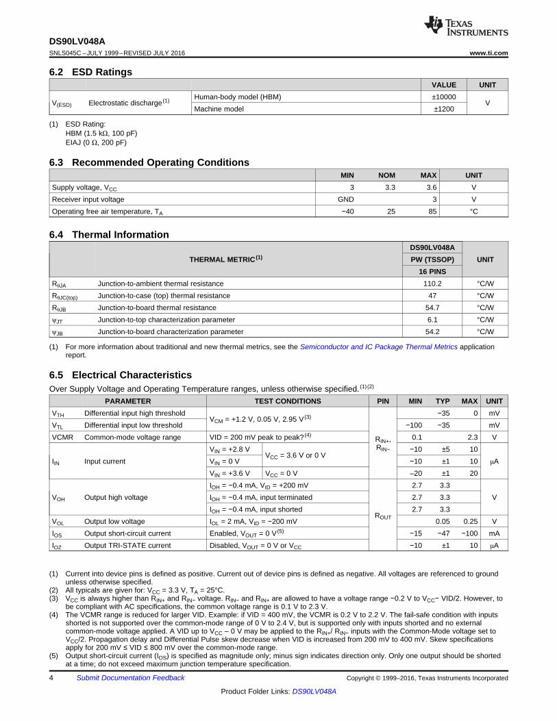
6.2 ESD RatingsVALUE UNIT
V(ESD) Electrostatic discharge (1) Human-body model (HBM) ±10000V
Machine model ±1200
6.3 Recommended Operating ConditionsMIN NOM MAX UNIT
Supply voltage, VCC 3 3.3 3.6 VReceiver input voltage GND 3 VOperating free air temperature, TA −40 25 85 °C
(1) For more information about traditional and new thermal metrics, see the Semiconductor and IC Package Thermal Metrics applicationreport.
6.4 Thermal Information
THERMAL METRIC (1)DS90LV048A
UNITPW (TSSOP)16 PINS
RθJA Junction-to-ambient thermal resistance 110.2 °C/WRθJC(top) Junction-to-case (top) thermal resistance 47 °C/WRθJB Junction-to-board thermal resistance 54.7 °C/WψJT Junction-to-top characterization parameter 6.1 °C/WψJB Junction-to-board characterization parameter 54.2 °C/W
(1) Current into device pins is defined as positive. Current out of device pins is defined as negative. All voltages are referenced to groundunless otherwise specified.
(2) All typicals are given for: VCC = 3.3 V, TA = 25°C.(3) VCC is always higher than RIN+ and RIN− voltage. RIN− and RIN+ are allowed to have a voltage range −0.2 V to VCC− VID/2. However, to
be compliant with AC specifications, the common voltage range is 0.1 V to 2.3 V.(4) The VCMR range is reduced for larger VID. Example: if VID = 400 mV, the VCMR is 0.2 V to 2.2 V. The fail-safe condition with inputs
shorted is not supported over the common-mode range of 0 V to 2.4 V, but is supported only with inputs shorted and no externalcommon-mode voltage applied. A VID up to VCC – 0 V may be applied to the RIN+/ RIN− inputs with the Common-Mode voltage set toVCC/2. Propagation delay and Differential Pulse skew decrease when VID is increased from 200 mV to 400 mV. Skew specificationsapply for 200 mV ≤ VID ≤ 800 mV over the common-mode range.
(5) Output short-circuit current (IOS) is specified as magnitude only; minus sign indicates direction only. Only one output should be shortedat a time; do not exceed maximum junction temperature specification.
6.5 Electrical CharacteristicsOver Supply Voltage and Operating Temperature ranges, unless otherwise specified. (1) (2)
PARAMETER TEST CONDITIONS PIN MIN TYP MAX UNITVTH Differential input high threshold
VCM = +1.2 V, 0.05 V, 2.95 V (3)
RIN+,RIN−
−35 0 mVVTL Differential input low threshold −100 −35 mVVCMR Common-mode voltage range VID = 200 mV peak to peak? (4) 0.1 2.3 V
IIN Input currentVIN = +2.8 V
VCC = 3.6 V or 0 V−10 ±5 10
μAVIN = 0 V −10 ±1 10VIN = +3.6 V VCC = 0 V –20 ±1 20
VOH Output high voltageIOH = −0.4 mA, VID = +200 mV
ROUT
2.7 3.3VIOH = −0.4 mA, input terminated 2.7 3.3
IOH = −0.4 mA, input shorted 2.7 3.3VOL Output low voltage IOL = 2 mA, VID = −200 mV 0.05 0.25 VIOS Output short-circuit current Enabled, VOUT = 0 V (5) −15 −47 −100 mAIOZ Output TRI-STATE current Disabled, VOUT = 0 V or VCC −10 ±1 10 μA
5
DS90LV048Awww.ti.com SNLS045C –JULY 1999–REVISED JULY 2016
Product Folder Links: DS90LV048A
Submit Documentation FeedbackCopyright © 1999–2016, Texas Instruments Incorporated
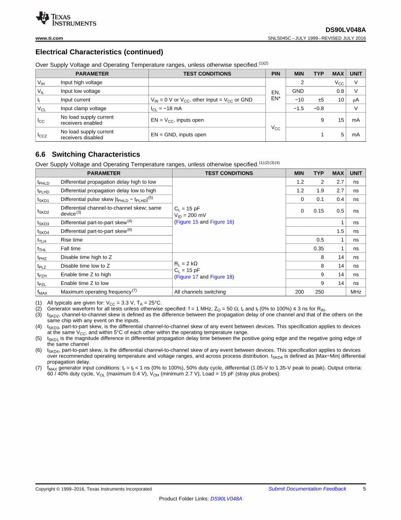
Electrical Characteristics (continued)Over Supply Voltage and Operating Temperature ranges, unless otherwise specified.(1)(2)
PARAMETER TEST CONDITIONS PIN MIN TYP MAX UNITVIH Input high voltage
EN,EN*
2 VCC VVIL Input low voltage GND 0.8 VII Input current VIN = 0 V or VCC, other Input = VCC or GND −10 ±5 10 μAVCL Input clamp voltage ICL = −18 mA −1.5 −0.8 V
ICCNo load supply currentreceivers enabled EN = VCC, inputs open
VCC
9 15 mA
ICCZNo load supply currentreceivers disabled EN = GND, inputs open 1 5 mA
(1) All typicals are given for: VCC = 3.3 V, TA = 25°C.(2) Generator waveform for all tests unless otherwise specified: f = 1 MHz, ZO = 50 Ω, tr and tf (0% to 100%) ≤ 3 ns for RIN.(3) tSKD2, channel-to-channel skew is defined as the difference between the propagation delay of one channel and that of the others on the
same chip with any event on the inputs.(4) tSKD3, part-to-part skew, is the differential channel-to-channel skew of any event between devices. This specification applies to devices
at the same VCC, and within 5°C of each other within the operating temperature range.(5) tSKD1 is the magnitude difference in differential propagation delay time between the positive going edge and the negative going edge of
the same channel(6) tSKD4, part-to-part skew, is the differential channel-to-channel skew of any event between devices. This specification applies to devices
over recommended operating temperature and voltage ranges, and across process distribution. tSKD4 is defined as |Max−Min| differentialpropagation delay.
(7) fMAX generator input conditions: tr = tf < 1 ns (0% to 100%), 50% duty cycle, differential (1.05-V to 1.35-V peak to peak). Output criteria:60 / 40% duty cycle, VOL (maximum 0.4 V), VOH (minimum 2.7 V), Load = 15 pF (stray plus probes).
6.6 Switching CharacteristicsOver Supply Voltage and Operating Temperature ranges, unless otherwise specified. (1) (2) (3) (4)
PARAMETER TEST CONDITIONS MIN TYP MAX UNITtPHLD Differential propagation delay high to low
CL = 15 pFVID = 200 mV(Figure 15 and Figure 16)
1.2 2 2.7 nstPLHD Differential propagation delay low to high 1.2 1.9 2.7 nstSKD1 Differential pulse skew |tPHLD − tPLHD| (5) 0 0.1 0.4 ns
tSKD2Differential channel-to-channel skew; samedevice (3) 0 0.15 0.5 ns
tSKD3 Differential part-to-part skew (4) 1 nstSKD4 Differential part-to-part skew (6) 1.5 nstTLH Rise time 0.5 1 nstTHL Fall time 0.35 1 nstPHZ Disable time high to Z
RL = 2 kΩCL = 15 pF(Figure 17 and Figure 18)
8 14 nstPLZ Disable time low to Z 8 14 nstPZH Enable time Z to high 9 14 nstPZL Enable time Z to low 9 14 nsfMAX Maximum operating frequency (7) All channels switching 200 250 MHz
6
DS90LV048ASNLS045C –JULY 1999–REVISED JULY 2016 www.ti.com
Product Folder Links: DS90LV048A
Submit Documentation Feedback Copyright © 1999–2016, Texas Instruments Incorporated
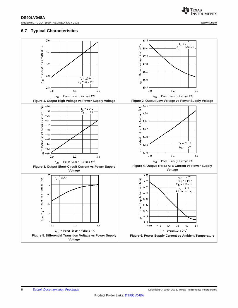
6.7 Typical Characteristics
Figure 1. Output High Voltage vs Power Supply Voltage Figure 2. Output Low Voltage vs Power Supply Voltage
Figure 3. Output Short-Circuit Current vs Power SupplyVoltage
Figure 4. Output TRI-STATE Current vs Power SupplyVoltage
Figure 5. Differential Transition Voltage vs Power SupplyVoltage
Figure 6. Power Supply Current vs Ambient Temperature
7
DS90LV048Awww.ti.com SNLS045C –JULY 1999–REVISED JULY 2016
Product Folder Links: DS90LV048A
Submit Documentation FeedbackCopyright © 1999–2016, Texas Instruments Incorporated
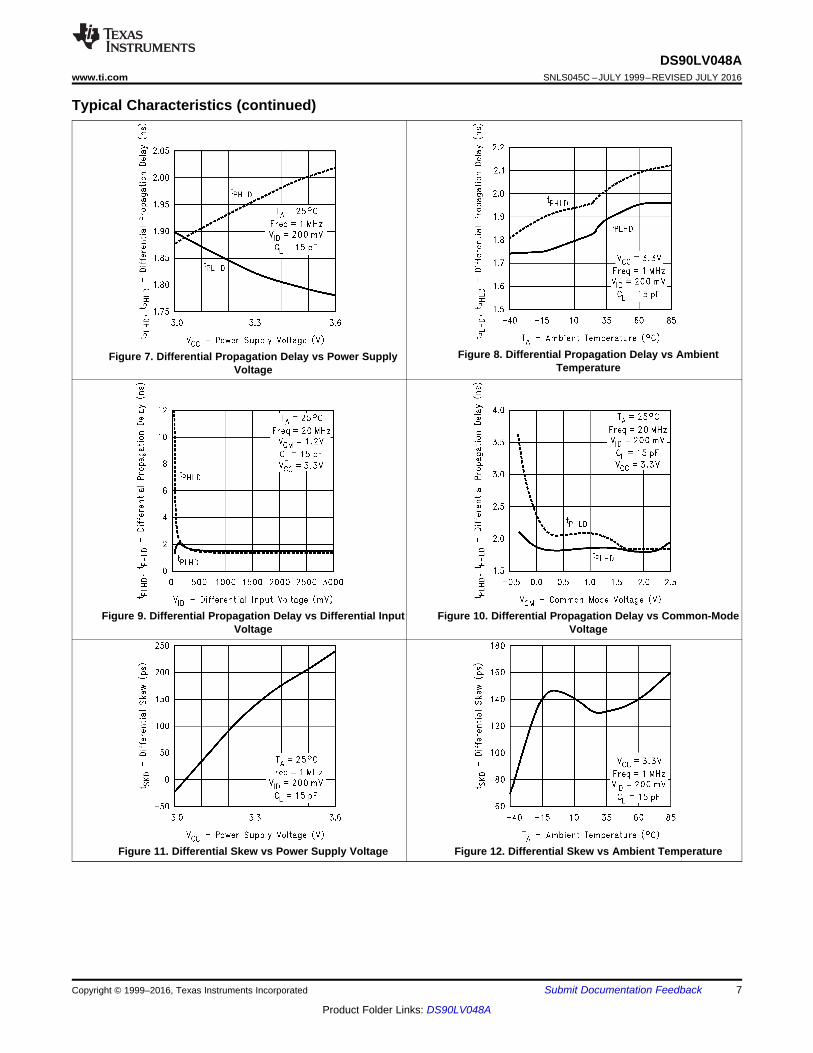
Typical Characteristics (continued)
Figure 7. Differential Propagation Delay vs Power SupplyVoltage
Figure 8. Differential Propagation Delay vs AmbientTemperature
Figure 9. Differential Propagation Delay vs Differential InputVoltage
Figure 10. Differential Propagation Delay vs Common-ModeVoltage
Figure 11. Differential Skew vs Power Supply Voltage Figure 12. Differential Skew vs Ambient Temperature
8
DS90LV048ASNLS045C –JULY 1999–REVISED JULY 2016 www.ti.com
Product Folder Links: DS90LV048A
Submit Documentation Feedback Copyright © 1999–2016, Texas Instruments Incorporated
Typical Characteristics (continued)
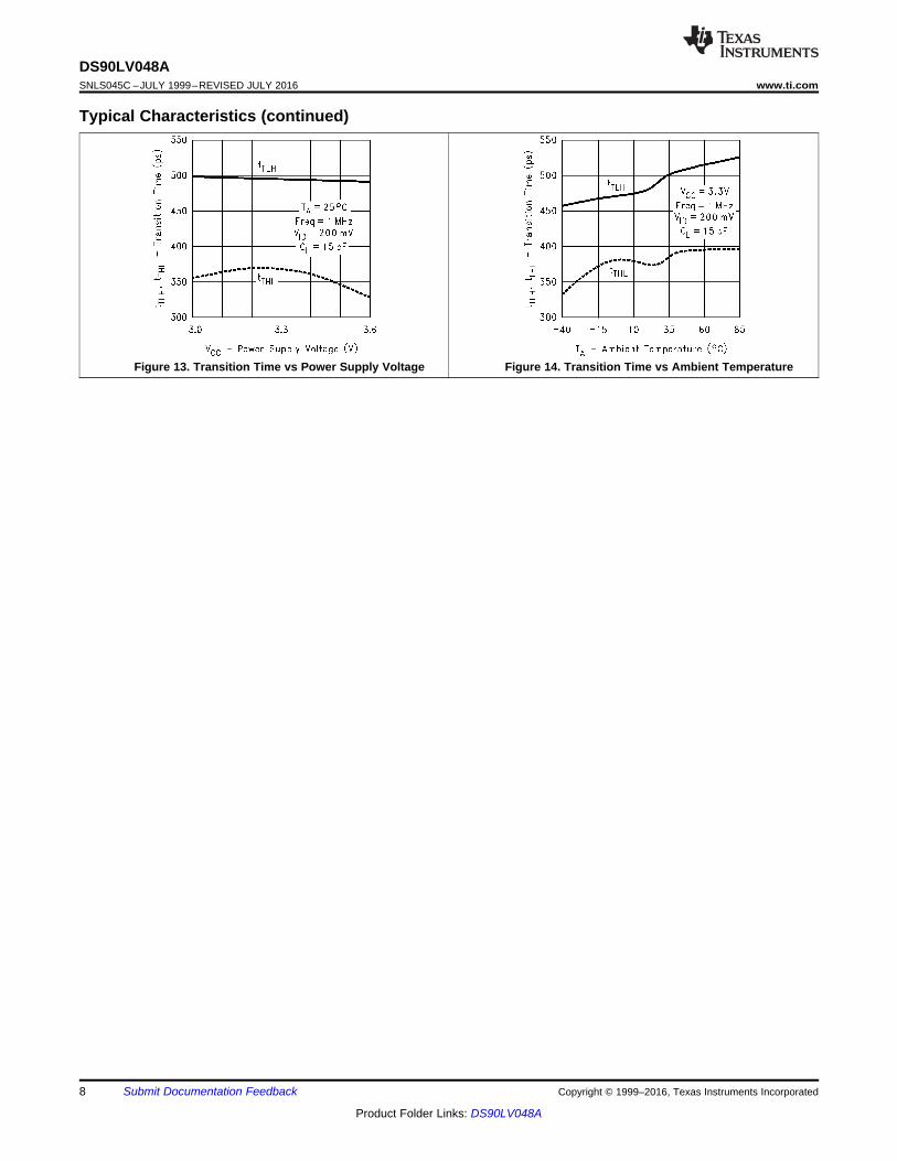
Figure 13. Transition Time vs Power Supply Voltage Figure 14. Transition Time vs Ambient Temperature
9
DS90LV048Awww.ti.com SNLS045C –JULY 1999–REVISED JULY 2016
Product Folder Links: DS90LV048A
Submit Documentation FeedbackCopyright © 1999–2016, Texas Instruments Incorporated
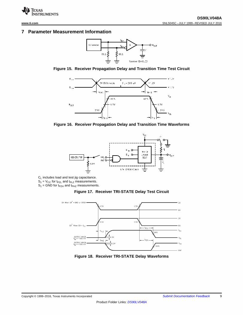
7 Parameter Measurement Information
Figure 15. Receiver Propagation Delay and Transition Time Test Circuit
Figure 16. Receiver Propagation Delay and Transition Time Waveforms
CL includes load and test jig capacitance.S1 = VCC for tPZL and tPLZ measurements.S1 = GND for tPZH and tPHZ measurements.
Figure 17. Receiver TRI-STATE Delay Test Circuit
Figure 18. Receiver TRI-STATE Delay Waveforms

10
DS90LV048ASNLS045C –JULY 1999–REVISED JULY 2016 www.ti.com
Product Folder Links: DS90LV048A
Submit Documentation Feedback Copyright © 1999–2016, Texas Instruments Incorporated
8 Detailed Description
8.1 OverviewLVDS drivers and receivers are intended to be primarily used in an uncomplicated point-to-point configuration asshown in Figure 19. This configuration provides a clean signaling environment for the fast edge rates of thedrivers. The receiver is connected to the driver through a balanced media which may be a standard twisted paircable, a parallel pair cable, or simply PCB traces. Typically, the characteristic impedance of the media is in therange of 100 Ω. A termination resistor of 100 Ω (selected to match the media) is located as close to the receiverinput pins as possible. The termination resistor converts the driver output (current mode) into a voltage that isdetected by the receiver. Other configurations are possible such as a multi-receiver configuration, but the effectsof a mid-stream connector(s), cable stub(s), and other impedance discontinuities as well as ground shifting, noisemargin limits, and total termination loading must be considered.
The DS90LV048A differential line receiver is capable of detecting signals as low as 100 mV, over a ±1-Vcommon-mode range centered around +1.2 V. This is related to the driver offset voltage which is typically +1.2 V.The driven signal is centered around this voltage and may shift ±1 V around this center point. The ±1-V shiftingmay be the result of a ground potential difference between the ground reference of the driver and the groundreference of the receiver, the common-mode effects of coupled noise, or a combination of the two. The ACparameters of both receiver input pins are optimized for a recommended operating input voltage range of 0 V to+2.4 V (measured from each pin to ground). The device operates for receiver input voltages up to VCC, butexceeding VCC turns on the ESD protection circuitry, which clamps the bus voltages.
The DS90LV048A has a flow-through pinout that allows for easy PCB layout. The LVDS signals on one side ofthe device easily allows for matching electrical lengths of the differential pair trace lines between the driver andthe receiver as well as allowing the trace lines to be close together to couple noise as common-mode. Noiseisolation is achieved with the LVDS signals on one side of the device and the TTL signals on the other side.
8.2 Functional Block Diagram
11
DS90LV048Awww.ti.com SNLS045C –JULY 1999–REVISED JULY 2016
Product Folder Links: DS90LV048A
Submit Documentation FeedbackCopyright © 1999–2016, Texas Instruments Incorporated
8.3 Feature Description
8.3.1 Fail-Safe FeatureThe LVDS receiver is a high-gain, high-speed device that amplifies a small differential signal (20 mV) to CMOSlogic levels. Due to the high gain and tight threshold of the receiver, take care to prevent noise from appearing asa valid signal.
The internal fail-safe circuitry of the receiver is designed to source or sink a small amount of current, providingfail-safe protection (a stable known state of HIGH output voltage) for floating, terminated or shorted receiverinputs.1. Open Input Pins. The DS90LV048A is a quad receiver device, and if an application requires only 1, 2, or 3
receivers, the unused channel(s) inputs must be left OPEN. Do not tie unused receiver inputs to ground orany other voltages. The input is biased by internal high value pullup and pulldown resistors to set the outputto a HIGH state. This internal circuitry ensures a HIGH, stable output state for open inputs.
2. Terminated Input. If the driver is disconnected (cable unplugged), or if the driver is in a TRI-STATE orpower-off condition, the receiver output is again in a HIGH state, even with the end of cable 100-Ωtermination resistor across the input pins. The unplugged cable can become a floating antenna which canpick up noise. If the cable picks up more than 10 mV of differential noise, the receiver may see the noise asa valid signal and switch. To ensure that any noise is seen as common-mode and not differential, a balancedinterconnect should be used. Twisted pair cable offers better balance than flat ribbon cable.
3. Shorted Inputs. If a fault condition occurs that shorts the receiver inputs together, thus resulting in a 0-Vdifferential input voltage, the receiver output remains in a HIGH state. Shorted input fail-safe is not supportedacross the common-mode range of the device (GND to 2.4 V). It is only supported with inputs shorted and noexternal common-mode voltage applied.
External lower value pullup and pulldown resistors (for a stronger bias) may be used to boost fail-safe in thepresence of higher noise levels. The pullup and pulldown resistors must be in the 5-kΩ to 15-kΩ range tominimize loading and waveform distortion to the driver. The common-mode bias point must be set toapproximately 1.2 V (less than 1.75 V) to be compatible with the internal circuitry.
Additional information on fail-safe biasing of LVDS devices may be found in AN-1194 Failsafe Biasing of LVDSInterfaces (SNLA051).
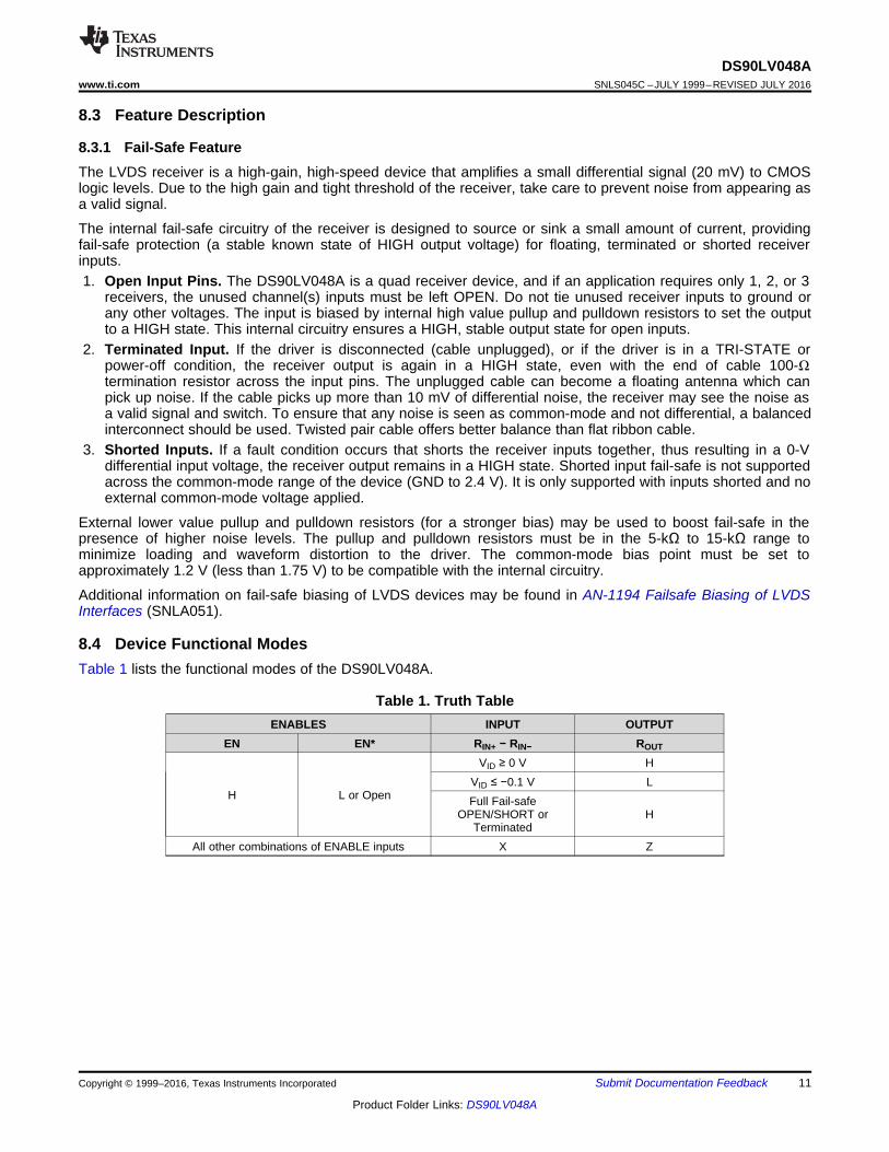
8.4 Device Functional ModesTable 1 lists the functional modes of the DS90LV048A.
Table 1. Truth TableENABLES INPUT OUTPUT
EN EN* RIN+ − RIN− ROUT
H L or Open
VID ≥ 0 V HVID ≤ −0.1 V LFull Fail-safe
OPEN/SHORT orTerminated
H
All other combinations of ENABLE inputs X Z

12
DS90LV048ASNLS045C –JULY 1999–REVISED JULY 2016 www.ti.com
Product Folder Links: DS90LV048A
Submit Documentation Feedback Copyright © 1999–2016, Texas Instruments Incorporated
9 Application and Implementation
NOTEInformation in the following applications sections is not part of the TI componentspecification, and TI does not warrant its accuracy or completeness. TI’s customers areresponsible for determining suitability of components for their purposes. Customers shouldvalidate and test their design implementation to confirm system functionality.
9.1 Application InformationThe DS90LV048A has a flow-through pinout that allows for easy PCB layout. The LVDS signals on one side ofthe device easily allows for matching electrical lengths of the differential pair trace lines between the driver andthe receiver as well as allowing the trace lines to be close together to couple noise as common-mode. Noiseisolation is achieved with the LVDS signals on one side of the device and the TTL signals on the other side.
9.2 Typical Application
Figure 19. Balanced System Point-to-Point Application
9.2.1 Design RequirementsWhen using LVDS devices, it is important to remember to specify controlled impedance PCB traces, cableassemblies, and connectors. All components of the transmission media must have a matched differentialimpedance of about 100 Ω. They must not introduce major impedance discontinuities.
Balanced cables (for example, twisted pair) are usually better than unbalanced cables (ribbon cable) for noisereduction and signal quality. Balanced cables tend to generate less EMI due to field canceling effects and alsotend to pick up electromagnetic radiation as common-mode (not differential mode) noise which is rejected by theLVDS receiver.
For cable distances < 0.5 M, most cables can be made to work effectively. For distances 0.5 M ≤ d ≤ 10 M,CAT5 (Category 5) twisted pair cable works well, is readily available, and relatively inexpensive.
9.2.2 Detailed Design Procedure
9.2.2.1 Probing LVDS Transmission LinesAlways use high impedance (> 100kΩ), low capacitance (< 2 pF) scope probes with a wide bandwidth (1 GHz)scope. Improper probing gives deceiving results.
9.2.2.2 ThresholdThe LVDS Standard (ANSI/TIA/EIA-644) specifies a maximum threshold of ±100 mV for the LVDS receiver. TheDS90LV048A supports an enhanced threshold region of −100 mV to 0 V. This is useful for fail-safe biasing. Thethreshold region is shown in the Voltage Transfer Curve (VTC) in Figure 20. The typical DS90LV048A LVDSreceiver switches at about −35 mV.
NOTEWith VID = 0 V, the output is in a HIGH state. With an external fail-safe bias of +25 mVapplied, the typical differential noise margin is now the difference from the switch point tothe bias point.
In the following example, this would be 60 mV of Differential Noise Margin (+25 mV − (−35 mV)). With theenhanced threshold region of −100 mV to 0 V, this small external fail-safe biasing of +25 mV (with respect to
13
DS90LV048Awww.ti.com SNLS045C –JULY 1999–REVISED JULY 2016
Product Folder Links: DS90LV048A
Submit Documentation FeedbackCopyright © 1999–2016, Texas Instruments Incorporated
Typical Application (continued)0 V) gives a DNM of a comfortable 60 mV. With the standard threshold region of ±100 mV, the external fail-safebiasing would need to be +25 mV with respect to +100 mV or +125 mV, giving a DNM of 160 mV which isstronger fail-safe biasing than is necessary for the DS90LV048A. If more DNM is required, then a stronger fail-safe bias point can be set by changing resistor values.
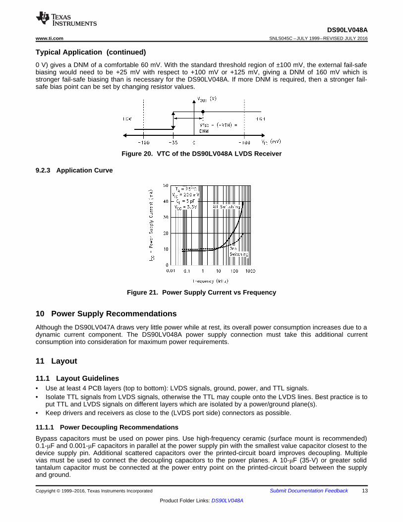
Figure 20. VTC of the DS90LV048A LVDS Receiver
9.2.3 Application Curve
Figure 21. Power Supply Current vs Frequency
10 Power Supply RecommendationsAlthough the DS90LV047A draws very little power while at rest, its overall power consumption increases due to adynamic current component. The DS90LV048A power supply connection must take this additional currentconsumption into consideration for maximum power requirements.
11 Layout
11.1 Layout Guidelines• Use at least 4 PCB layers (top to bottom): LVDS signals, ground, power, and TTL signals.• Isolate TTL signals from LVDS signals, otherwise the TTL may couple onto the LVDS lines. Best practice is to
put TTL and LVDS signals on different layers which are isolated by a power/ground plane(s).• Keep drivers and receivers as close to the (LVDS port side) connectors as possible.
11.1.1 Power Decoupling RecommendationsBypass capacitors must be used on power pins. Use high-frequency ceramic (surface mount is recommended)0.1-μF and 0.001-μF capacitors in parallel at the power supply pin with the smallest value capacitor closest to thedevice supply pin. Additional scattered capacitors over the printed-circuit board improves decoupling. Multiplevias must be used to connect the decoupling capacitors to the power planes. A 10-μF (35-V) or greater solidtantalum capacitor must be connected at the power entry point on the printed-circuit board between the supplyand ground.

8
7
Decoupling Cap
6
5
4
3
2
1
9
10
11
12
13
14
15
16
VCC
DIN2
DIN1
EN
DIN3
DIN4
EN*
GND
DOUT4-
DOUT4+
DOUT3+
DOUT3-
DOUT2-
DOUT2+
DOUT1+
DOUT1-
DS90LV047A
8
7
6
5
4
3
2
1
9
10
11
12
13
14
15
16
ROUT2
ROUT1
EN
ROUT3
ROUT4
EN*
GND
DS90LV048A
RIN4-
RIN4+
RIN3+
RIN3-
RIN2-
RIN2+
RIN1+
RIN1-
LVCMOS Inputs
VCCDecoupling Cap
Series Termination (optional)
Series Termination (optional)
LVCMOS Outputs
Input Termination (Required)
14
DS90LV048ASNLS045C –JULY 1999–REVISED JULY 2016 www.ti.com
Product Folder Links: DS90LV048A
Submit Documentation Feedback Copyright © 1999–2016, Texas Instruments Incorporated
Layout Guidelines (continued)11.1.2 Differential TracesUse controlled impedance traces that match the differential impedance of your transmission medium (that is,cable) and termination resistor. Run the differential pair trace lines as close together as possible as soon as theyleave the IC (stubs must be < 10 mm long). This helps eliminate reflections and ensure noise is coupled ascommon-mode. In fact, we have seen that differential signals which are 1 mm apart radiate far less noise thantraces 3 mm apart because magnetic field cancellation is much better with the closer traces. In addition, noiseinduced on the differential lines is much more likely to appear as common-mode which is rejected by thereceiver.
Match electrical lengths between traces to reduce skew. Skew between the signals of a pair means a phasedifference between signals, which destroys the magnetic field cancellation benefits of differential signals andEMI, results. Remember the velocity of propagation, v = c/Er where c (the speed of light) = 0.2997 mm/ps or0.0118 in/ps.
Do not rely solely on the autoroute function for differential traces. Carefully review dimensions to matchdifferential impedance and provide isolation for the differential lines. Minimize the number or vias and otherdiscontinuities on the line.
Avoid 90° turns (these cause impedance discontinuities). Use arcs or 45° bevels.
Within a pair of traces, the distance between the two traces should be minimized to maintain common-moderejection of the receivers. On the printed-circuit board, this distance must remain constant to avoid discontinuitiesin differential impedance. Minor violations at connection points are allowable.
11.1.3 TerminationUse a termination resistor that best matches the differential impedance or your transmission line. The resistormust be between 90 Ω and 130 Ω. Remember that the current mode outputs need the termination resistor togenerate the differential voltage. LVDS does not work without resistor termination. Typically, connecting a singleresistor across the pair at the receiver end will suffice.
Surface mount 1% to 2% resistors are best. PCB stubs, component lead, and the distance from the terminationto the receiver inputs must be minimized. The distance between the termination resistor and the receiver must be< 10 mm (12 mm maximum).
11.2 Layout Example
Figure 22. Layout Recommendation
15
DS90LV048Awww.ti.com SNLS045C –JULY 1999–REVISED JULY 2016
Product Folder Links: DS90LV048A
Submit Documentation FeedbackCopyright © 1999–2016, Texas Instruments Incorporated
12 Device and Documentation Support
12.1 Documentation Support
12.1.1 Related DocumentationFor related documentation, see the following:• LVDS Owner's Manual (SNLA187)• AN-808 Long Transmission Lines and Data Signal Quality (SNLA028)• AN-977 LVDS Signal Quality: Jitter Measurements Using Eye Patterns Test Report #1SNLA166)• AN-971 An Overview of LVDS Technology (SNLA165)• AN-916 A Practical Guide to Cable Selection (SNLA219)• AN-805 Calculating Power Dissipation for Differential Line Drivers (SNOA233)• AN-903 A Comparison of Differential Termination Techniques (SNLA034)• AN-1194 Failsafe Biasing of LVDS Interfaces (SNLA051)
12.2 Receiving Notification of Documentation UpdatesTo receive notification of documentation updates, navigate to the device product folder on ti.com. In the upperright corner, click on Alert me to register and receive a weekly digest of any product information that haschanged. For change details, review the revision history included in any revised document.
12.3 Community ResourcesThe following links connect to TI community resources. Linked contents are provided "AS IS" by the respectivecontributors. They do not constitute TI specifications and do not necessarily reflect TI's views; see TI's Terms ofUse.
TI E2E™ Online Community TI's Engineer-to-Engineer (E2E) Community. Created to foster collaborationamong engineers. At e2e.ti.com, you can ask questions, share knowledge, explore ideas and helpsolve problems with fellow engineers.
Design Support TI's Design Support Quickly find helpful E2E forums along with design support tools andcontact information for technical support.
12.4 TrademarksE2E is a trademark of Texas Instruments.All other trademarks are the property of their respective owners.
12.5 Electrostatic Discharge CautionThese devices have limited built-in ESD protection. The leads should be shorted together or the device placed in conductive foamduring storage or handling to prevent electrostatic damage to the MOS gates.
12.6 GlossarySLYZ022 — TI Glossary.
This glossary lists and explains terms, acronyms, and definitions.
13 Mechanical, Packaging, and Orderable InformationThe following pages include mechanical, packaging, and orderable information. This information is the mostcurrent data available for the designated devices. This data is subject to change without notice and revision ofthis document. For browser-based versions of this data sheet, refer to the left-hand navigation.

PACKAGE OPTION ADDENDUM
www.ti.com 8-Feb-2016
Addendum-Page 1
PACKAGING INFORMATION
Orderable Device Status(1)
Package Type PackageDrawing
Pins PackageQty
Eco Plan(2)
Lead/Ball Finish(6)
MSL Peak Temp(3)
Op Temp (°C) Device Marking(4/5)
Samples
DS90LV048ATM NRND SOIC D 16 48 TBD Call TI Call TI -40 to 85 DS90LV048ATM
DS90LV048ATM/NOPB ACTIVE SOIC D 16 48 Green (RoHS& no Sb/Br)
CU SN Level-1-260C-UNLIM -40 to 85 DS90LV048ATM
DS90LV048ATMTC NRND TSSOP PW 16 92 TBD Call TI Call TI -40 to 85 DS90LV048AT
DS90LV048ATMTC/NOPB ACTIVE TSSOP PW 16 92 Green (RoHS& no Sb/Br)
CU SN Level-1-260C-UNLIM -40 to 85 DS90LV048AT
DS90LV048ATMTCX NRND TSSOP PW 16 2500 TBD Call TI Call TI -40 to 85 DS90LV048AT
DS90LV048ATMTCX/NOPB ACTIVE TSSOP PW 16 2500 Green (RoHS& no Sb/Br)
CU SN Level-1-260C-UNLIM -40 to 85 DS90LV048AT
DS90LV048ATMX/NOPB ACTIVE SOIC D 16 2500 Green (RoHS& no Sb/Br)
CU SN Level-1-260C-UNLIM -40 to 85 DS90LV048ATM
(1) The marketing status values are defined as follows:ACTIVE: Product device recommended for new designs.LIFEBUY: TI has announced that the device will be discontinued, and a lifetime-buy period is in effect.NRND: Not recommended for new designs. Device is in production to support existing customers, but TI does not recommend using this part in a new design.PREVIEW: Device has been announced but is not in production. Samples may or may not be available.OBSOLETE: TI has discontinued the production of the device.
(2) Eco Plan - The planned eco-friendly classification: Pb-Free (RoHS), Pb-Free (RoHS Exempt), or Green (RoHS & no Sb/Br) - please check http://www.ti.com/productcontent for the latest availabilityinformation and additional product content details.TBD: The Pb-Free/Green conversion plan has not been defined.Pb-Free (RoHS): TI's terms "Lead-Free" or "Pb-Free" mean semiconductor products that are compatible with the current RoHS requirements for all 6 substances, including the requirement thatlead not exceed 0.1% by weight in homogeneous materials. Where designed to be soldered at high temperatures, TI Pb-Free products are suitable for use in specified lead-free processes.Pb-Free (RoHS Exempt): This component has a RoHS exemption for either 1) lead-based flip-chip solder bumps used between the die and package, or 2) lead-based die adhesive used betweenthe die and leadframe. The component is otherwise considered Pb-Free (RoHS compatible) as defined above.Green (RoHS & no Sb/Br): TI defines "Green" to mean Pb-Free (RoHS compatible), and free of Bromine (Br) and Antimony (Sb) based flame retardants (Br or Sb do not exceed 0.1% by weightin homogeneous material)
(3) MSL, Peak Temp. - The Moisture Sensitivity Level rating according to the JEDEC industry standard classifications, and peak solder temperature.
(4) There may be additional marking, which relates to the logo, the lot trace code information, or the environmental category on the device.
PACKAGE OPTION ADDENDUM
www.ti.com 8-Feb-2016
Addendum-Page 2
(5) Multiple Device Markings will be inside parentheses. Only one Device Marking contained in parentheses and separated by a "~" will appear on a device. If a line is indented then it is a continuationof the previous line and the two combined represent the entire Device Marking for that device.
(6) Lead/Ball Finish - Orderable Devices may have multiple material finish options. Finish options are separated by a vertical ruled line. Lead/Ball Finish values may wrap to two lines if the finishvalue exceeds the maximum column width.
Important Information and Disclaimer:The information provided on this page represents TI's knowledge and belief as of the date that it is provided. TI bases its knowledge and belief on informationprovided by third parties, and makes no representation or warranty as to the accuracy of such information. Efforts are underway to better integrate information from third parties. TI has taken andcontinues to take reasonable steps to provide representative and accurate information but may not have conducted destructive testing or chemical analysis on incoming materials and chemicals.TI and TI suppliers consider certain information to be proprietary, and thus CAS numbers and other limited information may not be available for release.
In no event shall TI's liability arising out of such information exceed the total purchase price of the TI part(s) at issue in this document sold by TI to Customer on an annual basis.
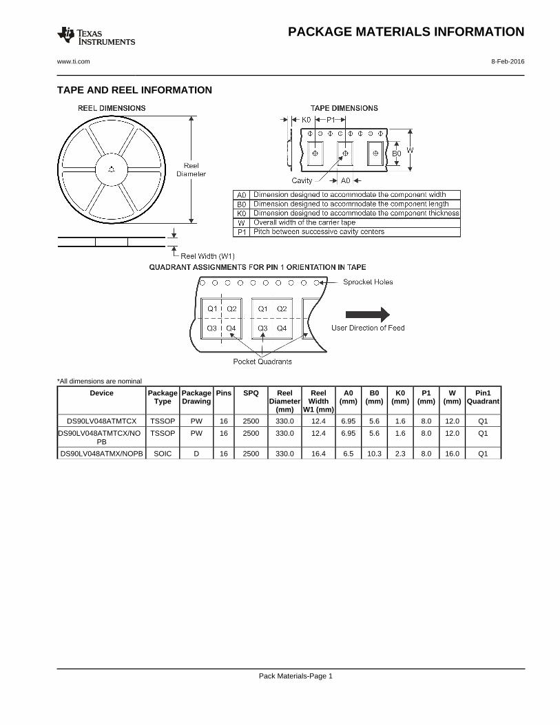
TAPE AND REEL INFORMATION
*All dimensions are nominal
Device PackageType
PackageDrawing
Pins SPQ ReelDiameter
(mm)
ReelWidth
W1 (mm)
A0(mm)
B0(mm)
K0(mm)
P1(mm)
W(mm)
Pin1Quadrant
DS90LV048ATMTCX TSSOP PW 16 2500 330.0 12.4 6.95 5.6 1.6 8.0 12.0 Q1
DS90LV048ATMTCX/NOPB
TSSOP PW 16 2500 330.0 12.4 6.95 5.6 1.6 8.0 12.0 Q1
DS90LV048ATMX/NOPB SOIC D 16 2500 330.0 16.4 6.5 10.3 2.3 8.0 16.0 Q1
PACKAGE MATERIALS INFORMATION
www.ti.com 8-Feb-2016
Pack Materials-Page 1

*All dimensions are nominal
Device Package Type Package Drawing Pins SPQ Length (mm) Width (mm) Height (mm)
DS90LV048ATMTCX TSSOP PW 16 2500 367.0 367.0 35.0
DS90LV048ATMTCX/NOPB
TSSOP PW 16 2500 367.0 367.0 35.0
DS90LV048ATMX/NOPB SOIC D 16 2500 367.0 367.0 35.0
PACKAGE MATERIALS INFORMATION
www.ti.com 8-Feb-2016
Pack Materials-Page 2


IMPORTANT NOTICE
Texas Instruments Incorporated and its subsidiaries (TI) reserve the right to make corrections, enhancements, improvements and otherchanges to its semiconductor products and services per JESD46, latest issue, and to discontinue any product or service per JESD48, latestissue. Buyers should obtain the latest relevant information before placing orders and should verify that such information is current andcomplete. All semiconductor products (also referred to herein as “components”) are sold subject to TI’s terms and conditions of salesupplied at the time of order acknowledgment.TI warrants performance of its components to the specifications applicable at the time of sale, in accordance with the warranty in TI’s termsand conditions of sale of semiconductor products. Testing and other quality control techniques are used to the extent TI deems necessaryto support this warranty. Except where mandated by applicable law, testing of all parameters of each component is not necessarilyperformed.TI assumes no liability for applications assistance or the design of Buyers’ products. Buyers are responsible for their products andapplications using TI components. To minimize the risks associated with Buyers’ products and applications, Buyers should provideadequate design and operating safeguards.TI does not warrant or represent that any license, either express or implied, is granted under any patent right, copyright, mask work right, orother intellectual property right relating to any combination, machine, or process in which TI components or services are used. Informationpublished by TI regarding third-party products or services does not constitute a license to use such products or services or a warranty orendorsement thereof. Use of such information may require a license from a third party under the patents or other intellectual property of thethird party, or a license from TI under the patents or other intellectual property of TI.Reproduction of significant portions of TI information in TI data books or data sheets is permissible only if reproduction is without alterationand is accompanied by all associated warranties, conditions, limitations, and notices. TI is not responsible or liable for such altereddocumentation. Information of third parties may be subject to additional restrictions.Resale of TI components or services with statements different from or beyond the parameters stated by TI for that component or servicevoids all express and any implied warranties for the associated TI component or service and is an unfair and deceptive business practice.TI is not responsible or liable for any such statements.Buyer acknowledges and agrees that it is solely responsible for compliance with all legal, regulatory and safety-related requirementsconcerning its products, and any use of TI components in its applications, notwithstanding any applications-related information or supportthat may be provided by TI. Buyer represents and agrees that it has all the necessary expertise to create and implement safeguards whichanticipate dangerous consequences of failures, monitor failures and their consequences, lessen the likelihood of failures that might causeharm and take appropriate remedial actions. Buyer will fully indemnify TI and its representatives against any damages arising out of the useof any TI components in safety-critical applications.In some cases, TI components may be promoted specifically to facilitate safety-related applications. With such components, TI’s goal is tohelp enable customers to design and create their own end-product solutions that meet applicable functional safety standards andrequirements. Nonetheless, such components are subject to these terms.No TI components are authorized for use in FDA Class III (or similar life-critical medical equipment) unless authorized officers of the partieshave executed a special agreement specifically governing such use.Only those TI components which TI has specifically designated as military grade or “enhanced plastic” are designed and intended for use inmilitary/aerospace applications or environments. Buyer acknowledges and agrees that any military or aerospace use of TI componentswhich have not been so designated is solely at the Buyer's risk, and that Buyer is solely responsible for compliance with all legal andregulatory requirements in connection with such use.TI has specifically designated certain components as meeting ISO/TS16949 requirements, mainly for automotive use. In any case of use ofnon-designated products, TI will not be responsible for any failure to meet ISO/TS16949.
Products ApplicationsAudio www.ti.com/audio Automotive and Transportation www.ti.com/automotiveAmplifiers amplifier.ti.com Communications and Telecom www.ti.com/communicationsData Converters dataconverter.ti.com Computers and Peripherals www.ti.com/computersDLP® Products www.dlp.com Consumer Electronics www.ti.com/consumer-appsDSP dsp.ti.com Energy and Lighting www.ti.com/energyClocks and Timers www.ti.com/clocks Industrial www.ti.com/industrialInterface interface.ti.com Medical www.ti.com/medicalLogic logic.ti.com Security www.ti.com/securityPower Mgmt power.ti.com Space, Avionics and Defense www.ti.com/space-avionics-defenseMicrocontrollers microcontroller.ti.com Video and Imaging www.ti.com/videoRFID www.ti-rfid.comOMAP Applications Processors www.ti.com/omap TI E2E Community e2e.ti.comWireless Connectivity www.ti.com/wirelessconnectivity
Mailing Address: Texas Instruments, Post Office Box 655303, Dallas, Texas 75265Copyright © 2016, Texas Instruments Incorporated