SMARTPHONE CONTROLLED POWER M
27
UNIVERSITY OF ILLINOIS AT URBANA-CHAMPAIGN SMARTPHONE CONTROLLED POWER METER DESIGN REVIEW Team Members: Shubham Pahadia Austin Chu Doni Tampubolon Teaching Assistant: Jackson Lenz ECE 445 October 16, 2016
Transcript of SMARTPHONE CONTROLLED POWER M

UNIVERSITY OF ILLINOIS AT URBANA-CHAMPAIGN
SMARTPHONE CONTROLLED POWER METER
DESIGN REVIEW
Team Members: Shubham Pahadia
Austin Chu Doni Tampubolon
Teaching Assistant: Jackson Lenz
ECE 445
October 16, 2016

Table of Contents
1 Introduction ......................................................................................................................... 1 1.1 The Problem ............................................................................................................................................................. 1 1.2 Our Solution ............................................................................................................................................................. 1 1.3 Objectives ................................................................................................................................................................. 1
1.3.1 Goals and Benefits .......................................................................................................................................... 1 1.3.2 Functionalities and Features .......................................................................................................................... 1
1.4 Existing Products ..................................................................................................................................................... 2 1.4.1 PXE Metered Rackmount Power Strips ...................................................................................................... 2 1.4.2 Watts Up .Net Electricity Consumption Meter .......................................................................................... 2
2 Design ................................................................................................................................ 3 2.1 Block Diagram ......................................................................................................................................................... 3 2.2 Block Description .................................................................................................................................................... 4
2.2.1 Smartphone Interface ..................................................................................................................................... 4 2.2.2 Microcontroller ................................................................................................................................................ 4 2.2.3 Bluetooth Module ............................................................................................................................................ 6 2.2.4 Power Sensor Unit .......................................................................................................................................... 7 2.2.5 Power Control Unit (Relay) ........................................................................................................................... 9 2.2.6 Full Wave Rectifier ........................................................................................................................................11 2.2.7 FlyBack Converter .........................................................................................................................................12 2.2.7 Design Alternatives .......................................................................................................................................13
5 Requirements and Verification ......................................................................................... 13 5.1 Requirements and Verification Points Breakdown ..........................................................................................13 5.2 Requirements and Verification Table .................................................................................................................13
6 Tolerance Analysis ............................................................................................................ 17 7 Financials & Schedule ...................................................................................................... 17
7.1 Financial Analysis ..................................................................................................................................................17 7.1.1 Labor ...............................................................................................................................................................17 7.1.2 Final Build Materials .....................................................................................................................................18 7.1.3 Financial Summary ........................................................................................................................................18
7.2 Schedule ..................................................................................................................................................................18 8 Ethics, Safety, and Citations ............................................................................................. 21
8.1 Ethics .......................................................................................................................................................................21 8.2 Safety .......................................................................................................................................................................21
8.2.1 Safety for Consumers ....................................................................................................................................21 8.2.1 Safety for Manufacturer and Developer ....................................................................................................22
8.3 Citations ..................................................................................................................................................................23

1
1 Introduction 1.1 The Problem
With the ever-rising prevalence of technology in our lives, we are all becoming increasingly aware of how much power our computers, televisions, and appliances are using. In order to minimize their electricity bills, some people will put their devices into sleep mode or unplug their devices. To track their power consumption, people would be forced to estimate based on their electricity bill or buy multiple power meters to get an idea of the energy being consumed. Unplugging appliances multiple times throughout the day is extremely cumbersome and time-consuming while merely putting devices to sleep still draws a small but significant amount of power. Using power meters can be accurate but there is no user-friendly way to observe all the info from various meters from one location and be able to act upon the knowledge.
1.2 Our Solution In order to be able to lower our electricity bills and energy consumption, we came up with the idea of creating power meter module with a smartphone interface that enables the user to view the power output from individual power outlets and remotely manage the power state of the outlet.
1.3 Objectives
1.3.1 Goals and Benefits
Ø Provide user with the ability to manage power status of outlets through a central hub Ø Modernize the ability of power tracking and consumption Ø Lower energy bill for users Ø User Friendly installation method
1.3.2 Functionalities and Features
Ø Smartphone application to allow hub control for easy manipulation and observation Ø Admin control for host via application to prevent security issues Ø Compact Design Ø Internal Switch Relay to control power to end load Ø Timer control to turn off power at set times based on user input

2
1.4 Existing Products
1.4.1 PXE Metered Rackmount Power Strips
The PXE Metered Rackmount Power Strips from Raritan provide a near identical service that we want to achieve, but at an exorbitant price range and are marketed towards business and IT consumers. They also have a variety of extra features such as environmental sensor support, and alert systems that are not necessary for the average customer and market base that we wish to target. Our concept reduces the functionalities and features in order to create a cost-effective and space-effective design for our targeted market base.
1.4.2 Watts Up .Net Electricity Consumption Meter
The Watts Up .NET Electricity Consumption Meter provides functionalities such as power switching and internet remote monitoring; however, it has a variety of problems and complaints from users that signify there are significant issues that need improvement. It suffers from a poor UI due to having 2 buttons to calculate data and is not user friendly so it becomes a hassle to install and use. Our design will differ in that primary control will be through a smartphone application and our design will be significantly smaller in size compared to the .NET Meter. Furthermore, we plan on having a more reasonable cost compared to the .NET Meter, which is roughly 250 dollars, due to size, material, and design improvements.

3
2 Design 2.1 Block Diagram
Figure 1: Overall System
Figure 2: High Level Block Diagram

4
2.2 Block Description
2.2.1 Smartphone Interface
The smartphone application will act as an interface between the end user and our project. The application will display the power being outputted at a set time period or at the current moment based on the user settings through data passed from the microcontroller to the Bluetooth module which then reaches the phone. Furthermore, we will implement a button that will tell the smartphone to send a wireless signal to the microcontroller in order to change the power status of the output from the outlet between on/off.
Figure 3: Title Screen View Figure 4: Outlet Screen 1 View
2.2.2 Microcontroller
The microcontroller is the brain and core of our device. It will be programmed by using an Arduino UNO as an AVR programmer in order to control the various other units of our device. The microcontroller will receive inputs from the voltage and current sensors and calculate the power. Then the microcontroller will send the calculated power to the Bluetooth module through SPI Protocol to then displayed by the smartphone application. In regards to the power control relay, based on the input from the user through the Bluetooth module, the microcontroller will either turn the power relay on or off. The ATmega328P - PU runs on 1.8 - 5.5 V with a operational range of -40 to 85 degrees Celsius with 28 pins. The max speed is 20 MHz. The ATmega328P - PU also has 6 channel 10-bit ADC resolution.

5
Figure 5: Maximum Frequency vs Vcc [12]
Figure 6: Microcontroller Pinout [12]

6
Table 1: Microcontroller Pins to Purpose Relationship
Pins Purpose/Connections
19 SCK - output for SPI clock
18 MISO - SPI input pin for data receiving
17 MOSI - SPI output pin for data sending
16 SS - SPI Slave Select pin
7 Vcc - 3.3 +- .3 VDC power input
23-28 Analog inputs - receiving data from power sensors
9-14 Digital outputs - sending data to power relay
2.2.3 Bluetooth Module
We will be using the Bluefruit nRF8001 Breakout v1.0 for our Bluetooth module. The chip will receive parameters from the smartphone and then pass them to the microcontroller in order to implement the wireless low power transmission of data across the application and device. It will also take the ASCII data from the microcontroller and pass it to the smartphone for viewing up to a range of 5 meters away from the device. The chip allows for SPI/UART Protocol Connection between the ATMega328P. We will be using SPI Protocol due to its faster data transmission speed compared to UART. Figure 7: Bluetooth Chip Image [10]

7
Table 2: Bluetooth Pins to Purpose Relationship
2.2.4 Power Sensor Unit
The power sensor we will be using consists of a voltage sensor and a current sensor. The voltage sensor we will be using is ZMPT101B single phase AC voltage sensor. The voltage sensor will measure the AC voltage coming out of the outlets in the power strip. The voltage sensor will then pass the reading to the microcontroller. The current sensor we will be using is ACS712 current sensor module. It will measure the amount of current that comes out of the outlets in the power strip. The reading from the current sensor module will then be passed to the microcontroller to be processed.
Figure 8: Voltage Sensor Chip Image [9]
Pins Purpose/Connections
SCK SPI data clock pin, connect to SPI master clock out
MISO SPI data out pin, outgoing data sent from this pin, data level is 3V
MOSI SPI data in pin, incoming data sent to this pin
REQ Basically the “Slave Select” input pin for SPI
RDY (ready) Data-ready pin, an interrupt output from the breakout to the microcontroller letting it know that data is ready to read
ACT (active) Output letting host know nRF8001 is busy
RST (reset) Reset pin input
3Vo Output from 3.3V regulator, up to 100mA from this pin
GND Ground for data and power
VIN 3.3 +- .3 VDC input to power module

8
Figure 9: Voltage Sensor Chip Circuit Design [9]
Table 3: Voltage Sensor Pins to Purpose Relationship
Figure 10: Current Sensor Chip Image [8]
Figure 11: Current Sensor Chip Circuit Design [8]
Pins Purpose
Neutral Terminals for voltage being sensed; fused internally
Phase Terminals for voltage being sensed; fused internally
VCC 5V supply voltage to power module
GND Ground
Out Analog output signal. The signal corresponds to the voltage reading.
FILT Terminal for external capacitor that sets bandwidth

9
Table 4: Current Sensor Pins to Purpose Relationship
2.2.5 Power Control Unit (Relay)
The power control unit will be used to switch ON/OFF the outlets in the strip. This unit is and electromagnetic-controlled mechanical switch. It will take a 5V input from the microcontroller in form of both power and a signal that dictates the ON/OFF status of the outlet. This unit provides another feature in our project as most basic power meters do not have a function of turning the power outlet on or off. The relay module we will be using has 4-channels. Figure 12: Power Relay Design and Layout [7]
Pins Purpose
IP+ Terminals for current being sensed; fused internally
IP- Terminals for current being sensed; fused internally
VCC 5V supply voltage to power module
GND Ground
Vout Analog output signal The voltage corresponds to the current reading.
FILTER Terminal for external capacitor that sets bandwidth

10
Figure 13: Power Relay Circuit Design [7]
Table 4: Power Relay Pins to Purpose Relationship
Pins Purpose/Connections
VCC Positive supply voltage (5V)
GND Ground
IN1 Relay control port 1
IN2 Relay control port 2
IN3 Relay control port 3
IN4 Relay control port 4

11
2.2.6 Full Wave Rectifier
Our product will be powered by the line AC voltage. However, the individual components in our device require smaller and different DC voltage inputs for power. Thus, we created a power regulator unit to convert the AC line voltage to the desired DC voltages. The power supply will first rectify the line AC voltage (120V Vrms) into a DC voltage (160±2.5V). Figure 14: Full Wave Rectifier Circuit Design
Figure 15: Full Wave Rectifier Voltage Ripple Output

12
2.2.7 FlyBack Converter
Figure 16: FlyBack Rudimentary Circuit Design
The Flyback Converter is used to step down the DC voltage of 160V from the Full Wave Rectifier to 3.3V+-0.3V. At the current moment, we are going to be supplying a direct 160V input instead of connecting it to our full wave rectifier in order to ensure that the circuit works. The diode D2 and resistor R2 are used as a snubber sub circuit in order to account for leakage from the primary inductor so that we are able to have a continuous mode instead of discontinuous mode converter. The BJT Transistor that is controlled from the microcontroller with a duty cycle of 60% in order to operate the flyback converter. The flyback converter works in the manner that while the switch is on, the voltage is isolated and kept in the air-gap, but when it turns off, it will transfer to the secondary inductor and then eventually provide current and voltage to the respective modules in our circuit. The transformer turn ratio is 240:5 in order to account for the duty cycle delay and step down accordingly.
Key Notes:
1 We plan on meeting with Professor Pilawa a second time next week in order to complete finalize the exact values for the flyback converter design. The circuit displayed operates without the snubber or BJT transistor as a switch, but we are still in the process of connecting the two remaining parts in order to finish our design.
2 We originally had a design for a flyback that would convert from 160V to both 5V DC and 3.3V DC, but due to complications in the circuit design, we opted not to follow through this path in order to ensure building a working flyback converter and stay within the scope of the class. Instead, we plan on having only a 3.3 V end output.
3 We chose a continuous mode of conversion to have less output voltage peaks in order to have a more consistent output so that we do not risk chance of breaking our smaller devices.

13
4 There are some potential EMI that we may encounter, so we plan on separating this part of the design from all the other smaller devices so that we do not run the risk of device failure.
2.2.7 Design Alternatives
MicroController • We could have used the ATMega168 instead, but we felt the ATMega328p was a
better choice because it offered more memory, so we would not run into a memory problem.
• We also planned on using an Arduino, but we opted to use the AtMega328P due to its ease of use, cost, and low power draw
Bluetooth Module • We originally planned to use Wi-Fi due to its superior range, but due to the massive
cost in power of Wi-Fi, we opted to use Bluetooth. Circuit Converter
• We could have used a linear regulator, a simple step-down transformer, or a variety of other methods of step down DC-DC circuits, but we decided on using the Flyback converter due to its low power consumption, efficiency in space, and accuracy.
Full Wave Rectifier • We chose to use a Full Wave Rectifier compared to Half-Wave Rectifier in order to
have consistent signal sent with no lows compared to the Half-Wave design.
5 Requirements and Verification 5.1 Requirements and Verification Points Breakdown
Bluetooth Unit – 10 points Microcontroller Unit – 20 points iOS Smartphone Application – 5 points Power Sensor Unit – 15 points AC to DC Voltage Converter – 40 points Control Relay – 10 points
5.2 Requirements and Verification Table
Requirements Verification
iOS Smartphone Application 1. Application opens and buttons work
Verification process for item 1: (a) Open iOS Application (b) Tap on desired outlet and ensure the
interface changes to show outlet selected (c) Tap on toggle button for power relay and
make sure the button slides from on to off and off to on.

14
Microcontroller Digital Output 1. Digital LOW corresponds to Vout ≤ 0.2 V 2. Digital HIGH corresponds to Vout ≥ 3.0 V
Verification process for item 1: (a) Power microcontroller with 3.3 V (b) Program all digital pins to output low (c) Ensure the multimeter shows Vout ≤ 0.2V for all output pins
Verification process for item 2: (a) Power microcontroller with 3.3 V (b) Program all digital pins to output low (c) Ensure the multimeter shows Vout ≥ 3.0V for all output pins
Microcontroller Digital Input 1. Digital LOW corresponds to Vout ≤ 0.2 V
2. Digital HIGH corresponds to Vout ≥ 3.0 V
Verification process for item 1: (a) Power microcontroller with 3.3 V (b) Attach digital pins to 0.2 V (c) Program Microcontroller to set all digital pins to input (d) Print pin values to Serial and make sure data values are 0
Verification process for item 2: (a) Power microcontroller with 3.3 V (b) Attach digital pins to 3.0 V (c) Program Microcontroller to set all digital pins to input (d) Print pin values to Serial and make sure data values are 1
Microcontroller Analog Input 1. Accurately read analog inputs from voltage and current sensors and quantize analog inputs to 0-1023
Verification process for item 1: (a) Power microcontroller with 3.3V (b) Attach all analog pins to variable voltage
source (c) Program Microcontroller to set all digital
pins to input (d) Print pin values to serial while sweeping
the input voltage from variable voltage source and ensure proper quantization
Bluetooth Module 1. Powered on 3.3V and functions properly
2. Must be able to send and receive ASCII data from both the microcontroller and smartphone.
Verification process for item 1: (a) Probe input voltage pin to ensure it is
3.3V (b) Check verification for items 2 and 3 of
the Bluetooth module to ensure proper functionality.
15
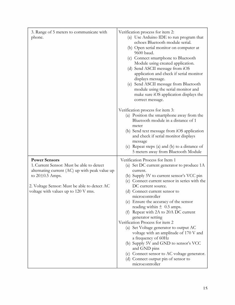
3. Range of 5 meters to communicate with phone.
Verification process for item 2: (a) Use Arduino IDE to run program that
echoes Bluetooth module serial. (b) Open serial monitor on computer at
9600 baud. (c) Connect smartphone to Bluetooth
Module using created application. (d) Send ASCII message from iOS
application and check if serial monitor displays message.
(e) Send ASCII message from Bluetooth module using the serial monitor and make sure iOS application displays the correct message.
Verification process for item 3:
(a) Position the smartphone away from the Bluetooth module in a distance of 1 meter
(b) Send text message from iOS application and check if serial monitor displays message
(c) Repeat steps (a) and (b) to a distance of 5 meters away from Bluetooth Module
Power Sensors 1. Current Sensor: Must be able to detect alternating current (AC) up with peak value up to 20±0.5 Amps.
2. Voltage Sensor: Must be able to detect AC voltage with values up to 120 V rms.
Verification Process for Item 1 (a) Set DC current generator to produce 1A
current. (b) Supply 5V to current sensor’s VCC pin (c) Connect current sensor in series with the
DC current source. (d) Connect current sensor to
microcontroller (e) Ensure the accuracy of the sensor
reading within ± 0.5 amps. (f) Repeat with 2A to 20A DC current
generator setting Verification Process for item 2
(a) Set Voltage generator to output AC voltage with an amplitude of 170 V and a frequency of 60Hz
(b) Supply 5V and GND to sensor’s VCC and GND pins
(c) Connect sensor to AC voltage generator. (d) Connect output pin of sensor to
microcontroller

16
(e) Ensure the voltage reading is within ±0.5V.
AC to DC Voltage Converter 1. AC voltage rectifier: Must output 160±2.5V for 230 mA load.
2. Switch mode DC/DC converter: Must step down 160 V DC voltage to 3.3 ± 0.3V for 230mA load
Verification Process for Item 1 (a) Attach 700 𝛀 resistor as load (b) Attach oscilloscope across load (c) Supply rectifier with 120 Vrms AC from wall
outlet. (d) Ensure output voltage remains within 162.5
V and 157.5 V
Verification Process for Item 2 (a) Attach 33 k𝛀 resistor as load (b) Attach oscilloscope across load (c) Supply regulator with 160 V DC (d) Ensure output voltage remains within 3 V
and 3.6 V
Power Control Module (Relay) 1. Must be able to switch from Normally Closed (NC) terminal to Normally Open (NO) terminal connection when a control coil is supplied with 5±0.5 V.
Verification Process for Item 1 (a) Connect a green LED to NC terminal, and a yellow LED to NO terminal, along with 330 Ohm resistors in series with the LEDs (b) set low voltage terminal of power supply to output 5V DC voltage (c) Connect the 5V to Relay module VCC pin (d) Connect ground from generator to ground pin of relay module (e) observe green LED. If it’s ON, the switch is connected to NC terminal, as desired. (f) connect 5V to the channel 1 input pin (g) observe yellow LED. If it’s ON, the relay has switched from NC to NO, i.e. the relay works as desired. (e) repeat for channels 2,3, and 4.

17
6 Tolerance Analysis Initially, we believed that the most critical component to our smart power strip device was going to be the integration of the power sensor module into the complete design, but after further analysis and review, we realized that the power converting and supply module is far more valuable to our design. If our Power Unit module fails to work, we run the risk of blowing out our microcontroller, Bluetooth device, and will not have an actual product. Since all of our devices will be running at 3.3V+-0.3V, we need to make sure that the voltage output is tuned accurately to 3.3 V+-0.3V. After adding up the current inputs necessary in order to drive the relay module, sensor systems, microcontroller, and Bluetooth for an individual outlet, we came to the conclusion that we needed 230 milliamps of current supplied total. If we account for the entire device, we will need 320 milliamps total. and we will be supplying a total 230 milliamps of current to the entire system, we will need to ensure that our supply unit yields this amount. Regarding current, there will be some leakage and issues coming from the use of the flyback converter, so we have decided to aim for a greater than necessary circuit output and then designate it accordingly in our design and connection to our individual modules. To show that tolerance is achieved, which means that the output from the power unit successful steps from 120V AC to 3.3V+-3.3 DC with 330mAmps, we can use the ammeter and/or voltmeter measure on a load at the output of the flyback converter and then verify that the correct current and voltage is supplied when measuring the input terminals at the individual modules. We have already detailed the values necessary to ensure that the circuit works and we get the correct tolerance above in our R&V table.
7 Financials & Schedule 7.1 Financial Analysis
7.1.1 Labor
Name Hourly Wage Hours Total Wage = Hourly Wage * Hours *
2.5
Shubham Pahadia $35/hour 160 hours $14,000
Doni Tampubolon $35/hour 160 hours $14,000
Austin Chu $35/hour 160 hours $14,000
Total $42,000

18
7.1.2 Final Build Materials
7.1.3 Financial Summary
7.2 Schedule
Week Task Delegation
9/12/2016 Submit Project Proposal Complete Lab Training
Shubham Pahadia
Doni Tampubolon
Austin Chu
9/19/2016 Begin Smartphone Application Dev.
Mock Design Review Write-Up Complete Eagle Assignment
Shubham Pahadia
Item Quantity Total Cost
ATmega328P 1 $2.18
Various Resistors/LEDS/Capacitors/ Potentiometers etc.
1 $5.00 from ECE Store/Electronics Services
Bluefruit LE nRF8001 Breakout 1 $19.95
Power Sensor Module 1 $2.85
4-Channel 5V Relay Module 1 $8.49
NPN BJT Transistor 1 $0.20
PLA 3D printed plastic 30 $4.50
ACS712 Current Sensor Breakout 4 $31.8
ZMPT101B Voltage Sensor 4 43.12
Total $118.09
Section Total
Labor $42,000
Parts $118.09
Total $42,118.09

19
Arrange meeting with machine shop Complete Eagle Assignment
Research relevant mathematical foundations for power monitoring and control
Doni Tampubolon
Begin Smartphone Application Dev. Complete Eagle Assignment
Research relevant mathematical foundations for power monitoring and control
Austin Chu
9/26/2016
Networking between smartphone and wireless module
Continue Smartphone Application Dev. Sign up for Design Review Design Review Write-Up
Shubham Pahadia
Design and Build Initial Power Control and Measuring Unit
Develop 1 circuit schematic and 1 plot for Mock Design Review
Doni Tampubolon
Continue Smartphone Application Dev. Design and Build Initial Power Control and
Measuring Unit Order/Assemble all parts
Austin Chu
10/3/2016
Present Design Review Continue Smartphone Application Dev.
Determine Parts and Design Improvements for Networking Module
Shubham Pahadia
Present Design Review Determine Parts and Design Improvements
for Sensor and Control Module Develop Circuit Schematics for Design
Review
Doni Tampubolon
Present Design Review Continue Smartphone Application Dev.
Determine Parts and Design Improvements for Sensor and Control Module
Austin Chu
10/10/2016
Complete Soldering Assignment Continue Smartphone Application
Integration of Networking and Power Units Shubham Pahadia
Complete Soldering Assignment Integration of Networking and Power Units
Doni Tampubolon
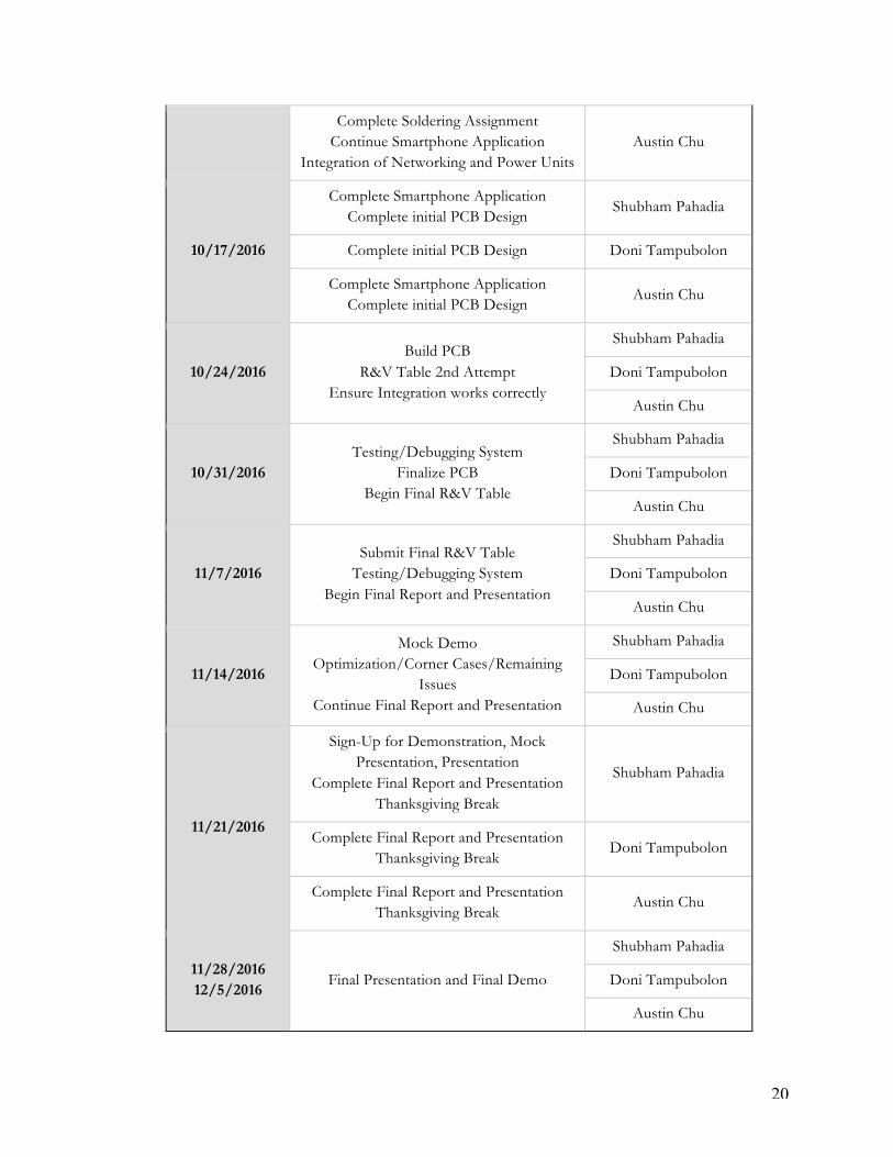
20
Complete Soldering Assignment Continue Smartphone Application
Integration of Networking and Power Units Austin Chu
10/17/2016
Complete Smartphone Application Complete initial PCB Design
Shubham Pahadia
Complete initial PCB Design Doni Tampubolon
Complete Smartphone Application Complete initial PCB Design
Austin Chu
10/24/2016 Build PCB
R&V Table 2nd Attempt Ensure Integration works correctly
Shubham Pahadia
Doni Tampubolon
Austin Chu
10/31/2016 Testing/Debugging System
Finalize PCB Begin Final R&V Table
Shubham Pahadia
Doni Tampubolon
Austin Chu
11/7/2016 Submit Final R&V Table
Testing/Debugging System Begin Final Report and Presentation
Shubham Pahadia
Doni Tampubolon
Austin Chu
11/14/2016
Mock Demo Optimization/Corner Cases/Remaining
Issues Continue Final Report and Presentation
Shubham Pahadia
Doni Tampubolon
Austin Chu
11/21/2016
Sign-Up for Demonstration, Mock Presentation, Presentation
Complete Final Report and Presentation Thanksgiving Break
Shubham Pahadia
Complete Final Report and Presentation Thanksgiving Break
Doni Tampubolon
Complete Final Report and Presentation Thanksgiving Break
Austin Chu
11/28/2016 12/5/2016
Final Presentation and Final Demo
Shubham Pahadia
Doni Tampubolon
Austin Chu

21
8 Ethics, Safety, and Citations 8.1 Ethics
The purpose of this project is to develop a remote controlled power meter strip that will track and control the power being used in a cost efficient manner. Our device will promote better power consumption habits and lower electricity consumption across the world. Our device is designed to improve the lives of others and therefore follows the first code of the IEEE Code of Ethics [1]: “To accept responsibility in making decisions consistent with the safety, health, and welfare of the public, and to disclose promptly factors that might endanger the public or the environment.” Through the process of completing this project, we will gain an increased understanding about power systems, micro controller processing, and Bluetooth and its interaction through wireless communication with mobile devices. We utilize our knowledge developed through our undergraduate experience and broaden our competence of operation and behavior of physical system as opposed to theoretical behavior. This aligns with the fifth and sixth code of the IEEE Code of Ethics [1]: “To improve the understanding of technology; its appropriate application, and potential consequences. To maintain and improve our technical competence and to undertake technological tasks for others only if qualified by training or experience, or after full disclosure of pertinent limitations.”
The process of designing and developing the system will involve consulting with teacher assistants, instructors, references, and varied other sources in order to improve our system design and change facets that are not optimal or realistic. Consequently, we will properly credit the contributions of others and cite all sources from which we developed our project. This process follows the seventh code of the IEEE Code of Ethics [1]: “to seek, accept, and offer honest criticism of technical work, to acknowledge and correct errors, and to credit properly the contributions of others”
8.2 Safety
8.2.1 Safety for Consumers
The Smart Power Strip will have all its components properly housed in a manner to minimize potential risks of harm to the consumer. However, there are still several precautions the consumer must take before and while using the Smart Power Strip.
Ø Do not immerse strip in water or liquids. Keep or store in a dry place. Ø Do not daisy-chain power strips. Ø Inspect Smart Power Strip for damages or deformities before use. Check for
cracked or frayed sockets, loose or bare wires, and loose connections. Ø Do not use cord in temperatures exceeding 85oC or below -50oC. It could lead to
overheating or malfunction of components inside power meter, and/or explosion or fire.

22
Ø Insert plugs fully into receptacle so that no part of the rings is exposed when the Power Strip is in use.
Ø Do not overload Power Strip with too many appliances or appliances wattage exceeding maximum capacity of the strip.
8.2.1 Safety for Manufacturer and Developer
In order to ensure there are no causalities during the design and manufacturing of the Smart Power Strip, there are several precautions the engineer must take while constructing the Smart Power Strip.
Ø Complete required lab safety training before entering the lab. Ø Proper attire must be worn inside lab premises. Ø Circuits should only be changed when power is not applied. Ø Use one handed method to probe or modify circuits. [2] Ø Before touching any elements, use an IR Measurement tool to detect temperature
and ensure nothing is too hot. Ø Check wiring and properly ground components before applying power. Ø Always work in the lab with a partner. Ø Wait an ample amount of time before manipulating capacitors or inductors in order
to ensure they have discharged. Ø Always maintain two points of contact with the bench supply and ground.

23
8.3 Citations
[1] IEEE Code of Ethics. Available: http://www.ieee.org/about/corporate/governance/p7-8.html [2] Power Safety Document. Available: Provided by TA [3] DC/DC Switching Regulator Basics [Online]. Available: http://micro.rohm.com/en/techweb/knowledge/dcdc/s-dcdc/02-s-dcdc/2642/ [4] Step-by-step for an Optimized Flyback Design [Online]. Available: http://www.power-eetimes.com/content/step-step-optimised-flyback-design [5] Transformer and Inductor Design Handbook, Chapter 13 [Online]. Available: http://coefs.uncc.edu/mnoras/files/2013/03/Transformer-and-Inductor-Design-Handbook_Chapter_13.pdf [6] Flyback Converter Design [Online]. Available: http://www.simonbramble.co.uk/dc_dc_converter_design/flyback_converter/flyback_converter_design.htm [7] 4-Channel 5V Relay Schematics [Online]. Available: https://www.sunfounder.com/wiki/index.php?title=4_Channel_5V_Relay_Module [8] ACS712 Current Sensor Breakout Datasheet [Online]. Available: http://cdn.sparkfun.com/datasheets/Sensors/Current/ACS712%20Breakout%20v11.pdf [9] ZMPT101B Voltage Sensor Datasheet [Online]. Available: http://makemyproduct.in/User/ProductDetailView.aspx?myID=1&subID=26&pId=1247 [10] Bluefruit LE Breakout Pinouts [Online]. Available: https://learn.adafruit.com/getting-started-with-the-nrf8001-bluefruit-le-breakout/pinouts [11] Bluetooth IC Module Datasheet [Online]. Available: http://www.nordicsemi.com/eng/Products/Bluetooth-low-energy/nRF8001 [12] ATmega328P Microcontroller Datasheet [Online]. Available: http://www.atmel.com/Images/Atmel-42735-8-bit-AVR-Microcontroller-ATmega328-328P_datasheet.pdf

1

2