Slow and Fast Light in Semiconductor Optical Amplifiers for ...cdn.intechweb.org/pdfs/13573.pdf ·...
27
0 Slow and Fast Light in Semiconductor Optical Amplifiers for Microwave Photonics Applications Perrine Berger 1 , Jérôme Bourderionnet 2 , Daniel Dolfi 3 , Fabien Bretenaker 4 and Mehdi Alouini 5 1,2,3 Thales Research and Technology 4 Laboratoire Aimé Cotton, CNRS - Université Paris Sud 5 Institut de Physique de Rennes France 1. Introduction The generation of continuously tunable optical delays and tunable phase shifts is a key element in microwave photonics. Among the targeted applications, one can quote the filtering of microwave signals, the synchronization of optoelectronics oscillators, and the control of optically fed phased array antennas. With these applications in view, large efforts are currently done in order to develop delay lines and phase shifters based on slow and fast light effects. To date, one of the most mature approaches for integration in real field systems is that based on Coherent Population Oscillations (CPO) in Semiconductor Optical Amplifiers (SOAs). This approach offers compactness, continuous tunability of the delay or phase shift through injected current control, and possible high-level parallelism. Slow and fast light capability of semiconductor devices has been first studied in the past decade while bearing in mind the delays, the phase shifts and the bandwidth they can offer. Consequently, in a first section, we present the recent advances in architectures based on slow and fast light in SOAs for microwave photonics applications. After a brief introduction about microwave photonics, we present the physical interpretation of the different architectures proposed in the literature. We point out the underlying physics, common to these architectures, and evidence the advantages and drawbacks of each of them. However, within the scope of integration in a realistic radar system, it is also required to study the impact of these slow and fast light architectures on the performances of the microwave photonics link. In particular, the RF transfer function, the generation of spurious signals by harmonic and intermodulation products, and the intensity noise, have to be studied in order to compute the Spurious Free Dynamic Range (SFDR), a key characteristic in microwave photonics. Consequently, in a second section, we present the tools to simulate and understand the RF transfer function, the generation of spurious signals through harmonic distortion and intermodulation products, and the intensity noise at the output of a SOA. In a third section, we use the models presented in the previous part in order to investigate the dynamic range of a microwave photonics link including an architecture based on slow and fast light in SOAs. We focus on the architecture using a SOA followed by an optical filter. The models are experimentally validated and the influence on the microwave photonics link is discussed. 9 www.intechopen.com
Transcript of Slow and Fast Light in Semiconductor Optical Amplifiers for ...cdn.intechweb.org/pdfs/13573.pdf ·...

0
Slow and Fast Light in Semiconductor OpticalAmplifiers for Microwave Photonics Applications
Perrine Berger1, Jérôme Bourderionnet2, Daniel Dolfi3,Fabien Bretenaker4 and Mehdi Alouini5
1,2,3Thales Research and Technology4Laboratoire Aimé Cotton, CNRS - Université Paris Sud
5Institut de Physique de RennesFrance
1. Introduction
The generation of continuously tunable optical delays and tunable phase shifts is a keyelement in microwave photonics. Among the targeted applications, one can quote the filteringof microwave signals, the synchronization of optoelectronics oscillators, and the control ofoptically fed phased array antennas. With these applications in view, large efforts are currentlydone in order to develop delay lines and phase shifters based on slow and fast light effects. Todate, one of the most mature approaches for integration in real field systems is that basedon Coherent Population Oscillations (CPO) in Semiconductor Optical Amplifiers (SOAs).This approach offers compactness, continuous tunability of the delay or phase shift throughinjected current control, and possible high-level parallelism.Slow and fast light capability of semiconductor devices has been first studied in the pastdecade while bearing in mind the delays, the phase shifts and the bandwidth they canoffer. Consequently, in a first section, we present the recent advances in architecturesbased on slow and fast light in SOAs for microwave photonics applications. After abrief introduction about microwave photonics, we present the physical interpretation ofthe different architectures proposed in the literature. We point out the underlying physics,common to these architectures, and evidence the advantages and drawbacks of each of them.However, within the scope of integration in a realistic radar system, it is also required to studythe impact of these slow and fast light architectures on the performances of the microwavephotonics link. In particular, the RF transfer function, the generation of spurious signalsby harmonic and intermodulation products, and the intensity noise, have to be studied inorder to compute the Spurious Free Dynamic Range (SFDR), a key characteristic in microwavephotonics. Consequently, in a second section, we present the tools to simulate and understandthe RF transfer function, the generation of spurious signals through harmonic distortion andintermodulation products, and the intensity noise at the output of a SOA.In a third section, we use the models presented in the previous part in order to investigate thedynamic range of a microwave photonics link including an architecture based on slow andfast light in SOAs. We focus on the architecture using a SOA followed by an optical filter.The models are experimentally validated and the influence on the microwave photonics linkis discussed.
9
www.intechopen.com

2. Background and context
2.1 Slow and fast light for microwave photonics
This section presents microwave photonics and explains why slow and fast light can be usefulfor this applied research field.
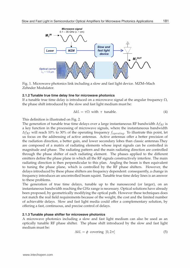
2.1.1 Microwave photonics link including a slow and fast light device
Microwave photonics realizes processing of microwave signals (Ω/2π ≃ 0.1 - 35 GHz) inthe optical domain using photonic devices. Indeed optics offer some advantages comparedto electronics for the addressing and processing of microwave signals: the most stickingasset is the low loss transport along an optical fiber (0.2 dB/km) compared to a coaxial cable(1000 dB/km !). As illustrated in Fig. 1, the basic architecture of a microwave photonics linkis composed of a laser, which creates the optical carrier (λ0 ≃ 1.5 µm). The optical carrieris modulated by the microwave signal either directly, or through an external Mach Zehndermodulator. Optical devices (represented on Fig. 1 by "slow and fast light device") process themodulated carrier. At the end of the link, a fast photodiode retrieves the processed microwavesignal.The aim of our study is to introduce a slow and fast light device in a microwave photonicslink, as it is represented in Fig. 1. Let us consider a monochromatic microwave signal(whose angular frequency is Ω) and a linear modulator, the optical field E after the modulatoris then composed of the optical carrier E0(z)e
−iω0t and two sidebands E1(z)e−i(ω0+Ω)t +
E−1(z)ei(ω0−Ω)t.
After propagation through the slow and fast light device, the microwave signal retrieved bythe photodiode, at the angular frequency Ω, is:
MOUT1 = ∑
ωp−ωq=Ω
EpE∗q , (1)
= E1E∗0 e
i(k1−k0)L + E∗−1E0e
i(k0−k−1)L, when both sidebands are detected,
= E1E∗0 e
i(k1−k0)L or E∗−1E0e
i(k0−k−1)L, when only one sideband is detected,
where L is the length of the dispersive medium (described by ki = k(ωi)).To characterize a microwave photonics link, we study the microwave transfer function
through the complex parameter S21 =MOUT
1MIN
1, whose magnitude and phase can be expressed
as:
|S21| = G2, (2)
arg(S21) = ΔkL, (3)
where G is the optical gain of the link, and ΔkL the phase shift introduced by the dispersivemedium (for example Δk = k(ω0 + Ω) − k(ω0) when only the sideband E1 is detected).Consequently, by governing the dispersion and in particular the optical group velocity vg =dωdk of the slow and fast light medium, it is possible to induce a controlled phase shift or delay
on the retrieved microwave signal, which is an important function in microwave photonics,as it is illustrated in the following sections.
180 Advances in Optical Amplifiers
www.intechopen.com
Laser
M1IN
MZM
Microwave signal
0.1 – 35 GHz (n"~ cm)
Optical carriern2 ~ 1.5 μm
RF,out RF,out M1OUT
Slow and
fast light
device
Fig. 1. Microwave photonics link including a slow and fast light device. MZM=MachZehnder Modulator.
2.1.2 Tunable true time delay line for microwave photonics
If a tunable true time delay is introduced on a microwave signal at the angular frequency Ω,the phase shift introduced by the slow and fast light medium must be:
ΔkL = τΩ with τ tunable. (4)
This definition is illustrated on Fig. 2.The generation of tunable true time delays over a large instantaneous RF bandwidth Δ fRF isa key function in the processing of microwave signals, where the instantaneous bandwidthΔ fRF will reach 10% to 30% of the operating frequency foperating. To illustrate this point, letus focus on the addressing of active antennas. Active antennas offer a better precision ofthe radiation direction, a better gain, and lower secondary lobes than classic antennas.Theyare composed of a matrix of radiating elements whose input signals can be controlled inmagnitude and phase. The radiating pattern and the main radiating direction are controlledthrough the phase shifter of each radiating element. The phases applied to the differentemitters define the phase plane in which all the RF signals constructively interfere. The mainradiating direction is then perpendicular to this plan. Angling the beam is then equivalentto tuning the phase plane, which is controlled by the RF phase shifters. However, thedelays introduced by these phase shifters are frequency dependent: consequently, a change infrequency introduces an uncontrolled beam squint. Tunable true time delay lines is an answerto these problems.The generation of true time delays, tunable up to the nanosecond (or larger), on aninstantaneous bandwidth reaching the GHz range is necessary. Optical solutions have alreadybeen proposed, by geometrically modifying the optical path. However these techniques doesnot match the real field requirements because of the weight, the cost and the limited numberof achievable delays. Slow and fast light media could offer a complementary solution, byoffering a fast, continuous, and precise control of delays.
2.1.3 Tunable phase shifter for microwave photonics
A microwave photonics including a slow and fast light medium can also be used as anoptically tunable RF phase shifter. The phase shift introduced by the slow and fast lightmedium must be:
ΔkL = φ covering [0, 2π] (5)
181Slow and Fast Light in Semiconductor Optical Amplifiers for Microwave Photonics Applications
www.intechopen.com

Phase f=FkL
RF frequency
(b) RF Phase shifter
foperating
FfRF
Phase f=FkL
RF frequencyfoperating
FfRF
(a) Tunable true time delay
v
Fig. 2. (a) Illustration of tunable true time delay. (b) Illustration of RF phase shifter.
This definition is illustrated on Fig. 2.This component exists in the microwave world (contrary to the true time delay lines).However, more and more RF functions are developed by photonic means. Consequently,tunable RF phase shifter in the optical domain is required in order to avoid uselessOptical/Electronical and Electronical/Optical conversions. Among the targeted applications,one can quote the filtering of microwave signals: on each arm a phase shifter overan instantaneous bandwidth Δ fRF is required; or optoelectronics oscillators, either forsynchronization or tunability: in this case, only a phase shifter at the operating frequencyis required.To date, one of the most mature approaches of slow and fast light medium for integration inreal field systems is that based on Coherent Population Oscillations (CPO) in semiconductoroptical amplifiers (SOAs). This approach offers compactness, continuous tunability of thedelay or phase shift through injected current control, and possible high-level parallelism. Wepresent in the following paragraphs the basic concepts of this technique.
2.2 Coherent Population Oscillations (CPO) in Semiconductor Optical Amplifier (SOA)
This section introduces the basic concepts and the main equations involved in CoherentPopulation Oscillations (CPO) in a Semiconductor Optical Amplifier (SOA), and explainshow this phenomenon induces slow and fast light. We describe the SOA behavior by aphenomenological model initially described for semiconductor lasers by Agrawal & Dutta(1993), and which was initially used to describe CPO in SOA (Agrawal, 1988; Mørk et al.,2005). It gives a good insight in the involved phenomena. However, this model, initiallydeveloped for lasers, must be cautiously used in the case of SOAs: its limitations are discussedin section 4, where a more rigorous model is developed. From this phenomenologicalmodel, we derive the equations of propagation and analyze the dispersion properties andin particular the changes in group velocity induced by CPO.
2.2.1 Phenomenological model of SOA
This phenomenological model of SOA, well described by Agrawal & Dutta (1993) is based onexperimental observations of the behavior of semiconductor lasers.The main assumption of the model consists in considering that the variations of the materialgain g and optical index n, caused by a small variation of the carrier density ΔN, areproportional to ΔN. The material gain g and the optical index n can thus be expressed as:
g = g + Δg, (6)
n = n + Δn, (7)
182 Advances in Optical Amplifiers
www.intechopen.com

with N and g = g(N) the static carrier density and gain, n = n((N)), the static optical index,and Δg and Δn the variations of the material gain and the optical index caused by a smallchange ΔN of the carrier density. We assume then:
Δg ∝ ΔN and Δn ∝ ΔN. (8)
We introduce the differential gain a:Δg = aΔN, (9)
and the linewidth enhancement factor α introduced by Henry (1982) to model the index gaincoupling in semiconductor material: α = −2k0
ΔnΓΔg . Then the variation Δn can be written as:
Δn = − α
2k0ΓΔg, (10)
with k0 = ωc , and Γ the confinement factor. We complete this phenomenological model with
a rate equation, which incorporates all the mechanisms by which the carriers are generated orlost in the active region:
dN
dt=
I
qV− N
τs− g|E|2
hω0, (11)
where I is the injected current, |E|2 is the optical intensity inside the SOA, τs is the carrierlifetime, V is the volume of the active region, q is the elementary charge, and ω0 is the angularfrequency of the optical carrier E0.
2.2.2 Coherent population oscillations
CPOs are induced by an optical carrier which is modulated in intensity at the angularfrequency Ω: |E|2 = M0 + M1e
−iΩt + c.c.. Note that the injected current can also be modulated(see section 3.3).If the optical carrier power is large enough, it implies a gain saturation. Indeed, the rateequation (11) shows that oscillations of the carriers (CPO) are induced : N = N + ΔNe−iΩt +c.c.. At the first order, we can assume a linear variation of the gain and optical index (Eq. 8):
g = g+ Δge−iΩt + c.c., (12)
n = n + Δne−iΩt + c.c. (13)
Finally the Eqs. 9 and 11 lead to the expression of the gain variation Δg (and then Δn thanksto Eq. 10):
Δg =A
1 + M0/Us − iΩτs, (14)
where M0 is the DC component of the optical intensity, Us the saturation intensity, and forsake of clarity, A is considered here as a constant (for example A = −gM1/Us when only theoptical intensity is modulated, see section 4).The optical index is then time and frequency dependent due to the CPO, which implies slowand fast propagation of the light, as we explain in the following paragraphs.
183Slow and Fast Light in Semiconductor Optical Amplifiers for Microwave Photonics Applications
www.intechopen.com

2.2.3 Equations of propagation
The optical field E(z, t) verifies the following wave equation:
∂2
∂2zE(z, t) =
1c2
∂2
∂2tǫscE(z, t), (15)
where ǫsc is the relative permittivity.
We expand the optical field as E(z, t) = ℜ
∑p Ep(z)ei(βpz−ωpt)
, where βp is the complex
propagation constant. E0 accounts for the optical carrier, and E±1 the modulation sidebandsat ω±1 = ω0 ± Ω. The complex propagation constant can be expressed as:
β = k0µ = k0√
ǫsc, (16)
with k0 = ωc and µ the complex optical index, which can be written as:
µ = n + i−Γg+ γ
2k0, (17)
where n is the real refractive optical index, and γ holds for internal losses. From Eqs. 12, 13and 17, the complex optical index µ can be expanded as: µ = µ0 + Δµe−iΩt + c.c., with:
µ0 = n +i
2k0(−Γg+ γ) ,
Δµ = − α + i
2k0ΓΔg. (18)
Lastly, we derive the equations of propagation from Eqs. 15, 18 and ǫsc = µ2:
dE0
dz=
12
(Γg− γ) E0,
dE1
dz=
12
(Γg− γ) E1 +1 − iα
2ΓΔgE0,
dE−1
dz=
12
(Γg− γ) E−1 +1 − iα
2ΓΔg∗E0. (19)
2.2.4 Slow and fast light induced by CPO
We have shown in the previous paragraph that the modulation of the optical intensity leadsto CPO, which induces a frequency dependence of the complex optical index. We illustratehere how it induces slow and fast light.We define the real, nr, and imaginary, nim, parts of the index: µ = nr + inim. The Eqs. 14 and18 lead to the following expressions of the variations of the real and imaginary parts of theoptical index, induced by CPO:
Δnr = ℜΔµ = − cA
2wα(1 + M0/Us) − Ωτs
(1 + M0/Us)2 + (Ωτs)2 , (20)
Δnim = ℑΔµ = − cA
2w(1 + M0/Us) + αΩτs
(1 + M0/Us)2 + (Ωτs)2 , (21)
where Ω is the angular frequency of the CPO, w is the angular frequency of the consideredoptical field component, and w = w0 + Ω with w0 the angular frequency of the optical carrier.
184 Advances in Optical Amplifiers
www.intechopen.com

−100 0 100
2wave n
um
ber
k (
m−
1)
detuning Ω (GHz)
c)c)
−20 −10 0 10 20−4
−2
0
2
4∆
nim
(x 1
0−
6)
detuning Ω (GHz)
a)a)
−20 −10 0 10 20
0
2
4
6
8
∆ n
r (x 1
0−
6)
detuning Ω (GHz)
b)b)10
−6
Fig. 3. Variations of (a) the imaginary part Δnim of the complex optical index (proportional tothe absorption), (b) the real part Δnr of the complex optical index, and (c) the wave number k.In blue, for semiconductor material (where α = 0), and in dashed red line, for an equivalent2-level atomic resonance (where α = 0). Parameters: α = 5 (blue line) or α = 0 (red dashedline), M0/Us = 1, A = −4000m−1, τs = 450ps, nsc = 3, λ0 = 1.5µm.
The variations of the imaginary Δnim and real Δnr parts of the optical index are displayed onFig.3(a) and (b). Δnim and Δnr are related by the Kramers-Kronig relationship. We illustratethat for semiconductor material, due to the coupling index-gain (modeled by the factor α), thevariation of the imaginary Δnim optical index, proportional to the variation of the absorption,is asymmetric: it has been first observed by Bogatov et al. (1975). The variation of the opticalindex with respect to the frequency is then very different from the case of 2-level atomicresonance (represented in dashed red line in Fig. 3).The frequency dependence of the optical index leads to a strong dispersion in the vicinity ofthe frequency of the optical carrier: as illustrated on Fig.3(c), the real wave number k(ω) =n(ω)ω
c differs then from the "normal" refraction nscωc (represented by the black dotted straight
line). This is associated with a variation of the group velocity of the light, which can be definedas vg = dω
dk . Consequently, CPO create here (A < 0) "fast light" for positive detuning Ω > 0
( dkdω < 0), and "slow light" for negative detuning Ω < 0 ( dk
dω > 0). In comparison, a 2-levelatomic resonance create essentially fast light at low detuning: |Ω| < a few GHz. As theamplitude of CPO is controlled by either the input optical power (M0) or the injected current(though the parameter A), the group velocity can be tuned and controlled, which opens thepossibility to conceive optical delay lines and optical phase shifters for microwave signals, aswe will explain it in the following part.The arrival time τ (to a detector for example) of a signal propagating through this slow and fastlight medium has to be carefully handled. Indeed it is equal to the group delay simply definedas τg = L dk
dω |ω, with ω the central optical frequency of the signal, only if the modulation beforethe photodiode is Single-SideBand (SSB), and if the bandwidth of the signal is smaller thanthe CPO bandwidth (< 1 GHz). We will highlight this last point in the following part. Forfurther details on the definition of the arrival time for optical pulses, you can refer to (Peatrosset al., 2000).
185Slow and Fast Light in Semiconductor Optical Amplifiers for Microwave Photonics Applications
www.intechopen.com
3. Advances in architectures based on slow and fast light in SOAs for microwave
photonics applications
In the previous part, we saw the underlying physics of the slow and fast light generated byCoherent Population Oscillations (CPO) in SOAs. We present here the different architecturesbased on this phenomenon, which are proposed for microwave photonics applications. Inthe first section, we present an architecture of an optical delay line. In the second section, weshow that by changing the modulation format before the photodiode, the latter architecturebecomes an optical phase shifter for microwave signals. Lastly, we present an alternativeset-up to realize an optical RF phase shifter, by using forced CPO.
3.1 SOA-based optical delay line
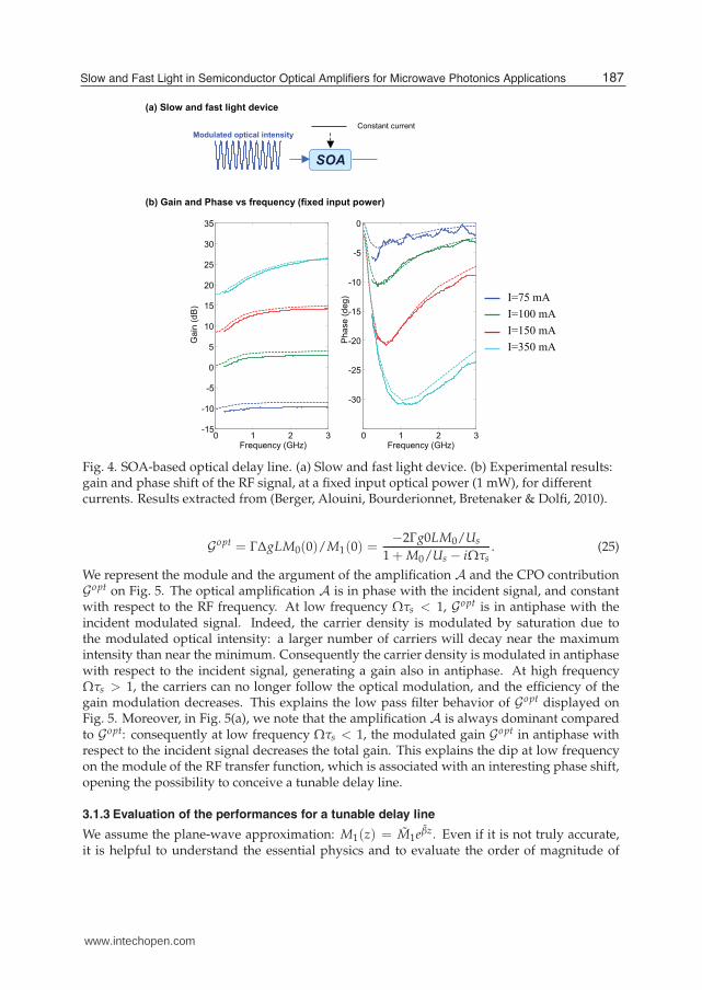
3.1.1 Set-up, experimental results and equations
This architecture is the first proposed in literature (Mørk et al., 2005; Pesala et al., 2006). Theset-up is quite simple: the slow and fast light device (represented in Fig. 1) included in themicrowave link is a single SOA. The corresponding experimental results are presented onFig. 4. The microwave gain |S21| present a high pass filter behavior, usually observed in SOAs(Boula-Picard et al., 2005), and is associated to an interesting phase shift, which presents alinear variation at low frequency, with a slope tunable through the injected current or theoptical input power: a key characteristic to set up a tunable delay line (see Fig. 2).These results are not in adequation with the expected behavior of a semiconductor materialin which the coupling index-gain is significant (α = 0) (displayed in Fig. 3), but it is similarto the material where α = 0: indeed a negative delay (which is then an advance, associatedto a so called "fast light") is detected at low frequency (< GHz). However it can be easilyexplained by the double-sideband modulation format before the detector. Indeed, as boththe modulation sidebands are detected, the RF retrieved signal at the angular frequency Ω isM1 = E1E
∗0 + E−1E
∗0 , and Eq. 19 leads to:
dM1
dz= [−γ + Γg] M1 + ΓΔgM0, (22)
with Δg deduced from the rate equation (11):
Δg = − gM1/Us
1 + M0/Us − iΩτs, (23)
with Us = hωΓaτs
. We notice then that the contribution of the coupling gain-index is canceledout when both the sidebands are detected, which explains that the gain and phase shift aresimilar to a material where α = 0.
3.1.2 Analysis of the different contributions. Physical interpretation
We integrate Eq. 22 over a small slice dz, whose length is noted L, to derive an analytical
expression of the RF transfer function S21 = M1(L)M1(0)
:
M1(L)
M1(0)= A +
12Gopt, (24)
with A = 1− γL+ ΓgL corresponding to the optical amplification (average RF gain) and Gopt
the contribution due to CPO, which are induced by the modulation of the optical intensity:
186 Advances in Optical Amplifiers
www.intechopen.com
(b) Gain and Phase vs frequency (fixed input power)
SOA
Constant current
(a) Slow and fast light device
Modulated optical intensity
0 1 2 3-15
-10
-5
0
5
10
15
20
25
30
35
Frequency (GHz)
Ga
in (
dB
)
0 1 2 3
-30
-25
-20
-15
-10
-5
0
Frequency (GHz)
Ph
ase
(d
eg
) I=75 mA
I=100 mA
I=150 mA
I=350 mA
Fig. 4. SOA-based optical delay line. (a) Slow and fast light device. (b) Experimental results:gain and phase shift of the RF signal, at a fixed input optical power (1 mW), for differentcurrents. Results extracted from (Berger, Alouini, Bourderionnet, Bretenaker & Dolfi, 2010).
Gopt = ΓΔgLM0(0)/M1(0) =−2Γg0LM0/Us
1 + M0/Us − iΩτs. (25)
We represent the module and the argument of the amplification A and the CPO contributionGopt on Fig. 5. The optical amplification A is in phase with the incident signal, and constantwith respect to the RF frequency. At low frequency Ωτs < 1, Gopt is in antiphase with theincident modulated signal. Indeed, the carrier density is modulated by saturation due tothe modulated optical intensity: a larger number of carriers will decay near the maximumintensity than near the minimum. Consequently the carrier density is modulated in antiphasewith respect to the incident signal, generating a gain also in antiphase. At high frequencyΩτs > 1, the carriers can no longer follow the optical modulation, and the efficiency of thegain modulation decreases. This explains the low pass filter behavior of Gopt displayed onFig. 5. Moreover, in Fig. 5(a), we note that the amplification A is always dominant comparedto Gopt: consequently at low frequency Ωτs < 1, the modulated gain Gopt in antiphase withrespect to the incident signal decreases the total gain. This explains the dip at low frequencyon the module of the RF transfer function, which is associated with an interesting phase shift,opening the possibility to conceive a tunable delay line.
3.1.3 Evaluation of the performances for a tunable delay line
We assume the plane-wave approximation: M1(z) = M1eβz. Even if it is not truly accurate,
it is helpful to understand the essential physics and to evaluate the order of magnitude of
187Slow and Fast Light in Semiconductor Optical Amplifiers for Microwave Photonics Applications
www.intechopen.com

0,01 0,1 1 10 -10
-5
0
5
10
15
20
25
Y vs
Ga
in (
dB
)
(b) Optical filtering
0,01 0,1 1 10
-200
-150
-100
-50
0
Ph
as
e (
°)
CPO
contribution
Amplification
Total RF transfer
function
Total RF transfer
functionCPO
contribution
Amplification
antiphase
Fig. 5. Contributions and resulting total transfer function.
achievable delay and bandwidth. From Eq. 22, we can deduce the complex propagationconstant β:
βL = −i
(
−γL+ ΓgL− ΓgLM0/Us
1 + M0/Us − iΩτs
)
. (26)
After a small slice dz, if we assume that the gain compensates losses, the output signal is then:GRFM1(0)e−iΩ(t−τ), with:
τ = − ΓgLM0/Us
(1 + M0/Us)2 + (Ωτs)2 τs (27)
≃ − ΓgLM0/Us
(1 + M0/Us)2 τs at low frequency Ωτs < 1 + M0/Us. (28)
Consequently, at low frequency, CPO introduce a true time advance τ (negative delay,independent on the frequency Ω): Eq. 28 gives the limit of the achievable delay andbandwidth.It is possible to make a rough evaluation of the maximal achievable bandwidth-delay product,by assuming the saturation parameters (Us, τs, ΓgL) constant with the current and the inputoptical power :
(Δ fRF ∗ τ)max <1
2π
M0/Us
1 + M0/Us(ΓgL)max . (29)
The higher the input optical power M0 is, the higher the bandwidth-delay product is. ASOA with a high gain is suitable. However the maximal advance (negative delay) achievablefor a given current is: τM(I) = − 1
4 ΓgLτs for a strong input optical power M0/Us ∼ 1.The delays are tunable from 0 to τM(Imax)(< 0), as the gain gL governed by the injectedcurrent I. The delay is null at the transparency, and can be positive when the SOA is inthe absorption regime (but it is associated with high losses on the RF signal). In order torefine the performances, and take into account saturation effects, we use the mean saturation
188 Advances in Optical Amplifiers
www.intechopen.com
parameters (Us, τs, ΓgL) along the SOA, calculated from the model presented in section 4,for a given current and input optical power. For example, a commercial SOA (InP/InGaAsPQuantum Well Booster Amplifier from COVEGA) has a maximal tunable advance of ≈ 516ps(≈ 120ps) over an instantaneous bandwidth < 590MHz (< 410MHz) for an input opticalpower of 20mW (1mW).The major axes of research are now to find the best material to increase these performances,and try to find an architecture which enables to translate these characteristics at any operatingfrequency.
3.2 CPO enhanced by index-grating coupling
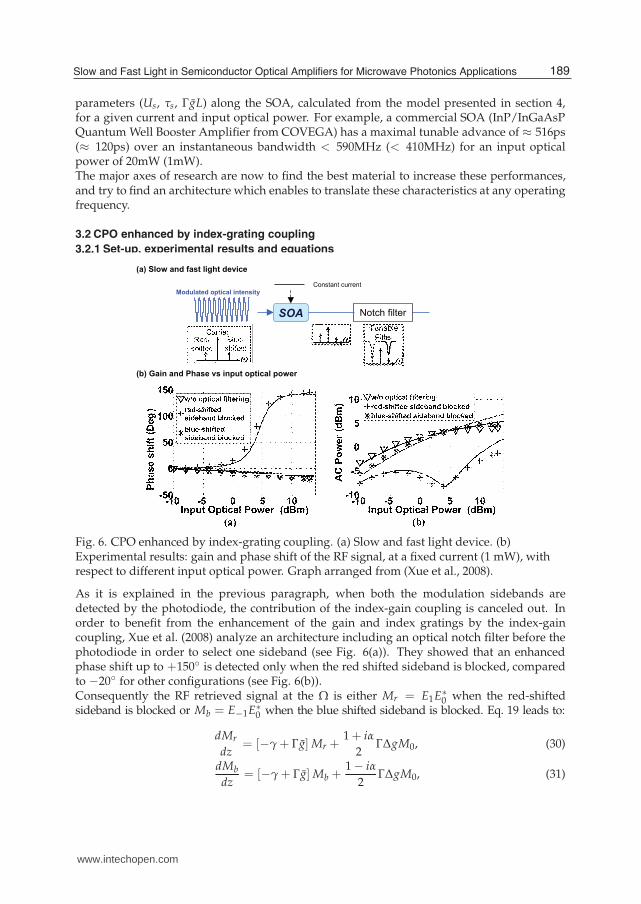
3.2.1 Set-up, experimental results and equations
(b) Gain and Phase vs input optical power
SOA
Constant current
(a) Slow and fast light device
Modulated optical intensity
Notch filter
Fig. 6. CPO enhanced by index-grating coupling. (a) Slow and fast light device. (b)Experimental results: gain and phase shift of the RF signal, at a fixed current (1 mW), withrespect to different input optical power. Graph arranged from (Xue et al., 2008).
As it is explained in the previous paragraph, when both the modulation sidebands aredetected by the photodiode, the contribution of the index-gain coupling is canceled out. Inorder to benefit from the enhancement of the gain and index gratings by the index-gaincoupling, Xue et al. (2008) analyze an architecture including an optical notch filter before thephotodiode in order to select one sideband (see Fig. 6(a)). They showed that an enhancedphase shift up to +150 is detected only when the red shifted sideband is blocked, comparedto −20 for other configurations (see Fig. 6(b)).Consequently the RF retrieved signal at the Ω is either Mr = E1E
∗0 when the red-shifted
sideband is blocked or Mb = E−1E∗0 when the blue shifted sideband is blocked. Eq. 19 leads to:
dMr
dz= [−γ + Γg] Mr +
1 + iα
2ΓΔgM0, (30)
dMb
dz= [−γ + Γg] Mb +
1 − iα
2ΓΔgM0, (31)
189Slow and Fast Light in Semiconductor Optical Amplifiers for Microwave Photonics Applications
www.intechopen.com
with Δg defined by Eq. 23.
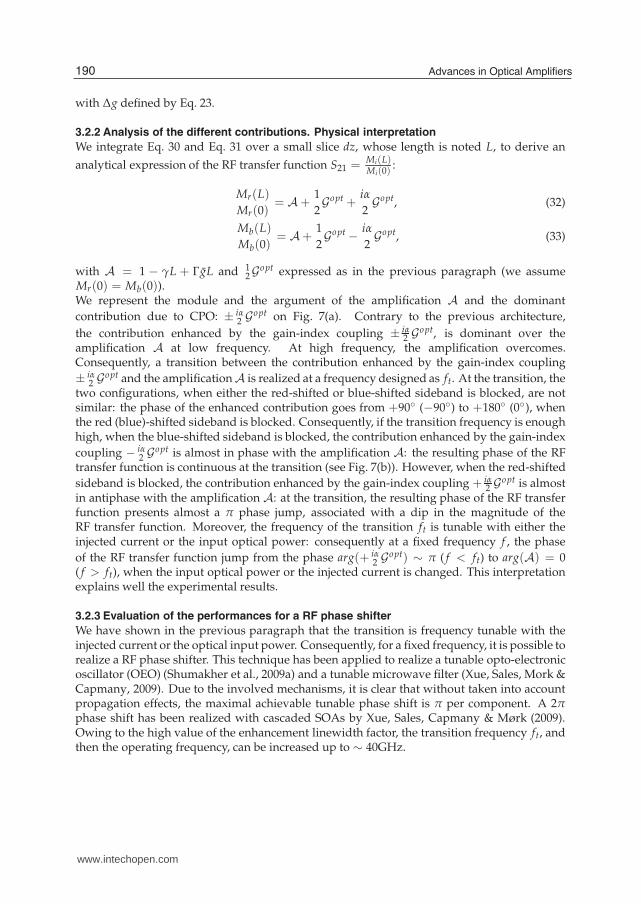
3.2.2 Analysis of the different contributions. Physical interpretation
We integrate Eq. 30 and Eq. 31 over a small slice dz, whose length is noted L, to derive an
analytical expression of the RF transfer function S21 =Mi(L)Mi(0)
:
Mr(L)
Mr(0)= A +
12Gopt +
iα
2Gopt, (32)
Mb(L)
Mb(0)= A+
12Gopt − iα
2Gopt, (33)
with A = 1 − γL + ΓgL and 12Gopt expressed as in the previous paragraph (we assume
Mr(0) = Mb(0)).We represent the module and the argument of the amplification A and the dominantcontribution due to CPO: ± iα
2 Gopt on Fig. 7(a). Contrary to the previous architecture,the contribution enhanced by the gain-index coupling ± iα
2 Gopt, is dominant over theamplification A at low frequency. At high frequency, the amplification overcomes.Consequently, a transition between the contribution enhanced by the gain-index coupling± iα
2 Gopt and the amplification A is realized at a frequency designed as ft. At the transition, thetwo configurations, when either the red-shifted or blue-shifted sideband is blocked, are notsimilar: the phase of the enhanced contribution goes from +90 (−90) to +180 (0), whenthe red (blue)-shifted sideband is blocked. Consequently, if the transition frequency is enoughhigh, when the blue-shifted sideband is blocked, the contribution enhanced by the gain-indexcoupling − iα
2 Gopt is almost in phase with the amplification A: the resulting phase of the RFtransfer function is continuous at the transition (see Fig. 7(b)). However, when the red-shiftedsideband is blocked, the contribution enhanced by the gain-index coupling + iα
2 Gopt is almostin antiphase with the amplification A: at the transition, the resulting phase of the RF transferfunction presents almost a π phase jump, associated with a dip in the magnitude of theRF transfer function. Moreover, the frequency of the transition ft is tunable with either theinjected current or the input optical power: consequently at a fixed frequency f , the phaseof the RF transfer function jump from the phase arg(+ iα
2 Gopt) ∼ π ( f < ft) to arg(A) = 0( f > ft), when the input optical power or the injected current is changed. This interpretationexplains well the experimental results.
3.2.3 Evaluation of the performances for a RF phase shifter
We have shown in the previous paragraph that the transition is frequency tunable with theinjected current or the optical input power. Consequently, for a fixed frequency, it is possible torealize a RF phase shifter. This technique has been applied to realize a tunable opto-electronicoscillator (OEO) (Shumakher et al., 2009a) and a tunable microwave filter (Xue, Sales, Mork &Capmany, 2009). Due to the involved mechanisms, it is clear that without taken into accountpropagation effects, the maximal achievable tunable phase shift is π per component. A 2πphase shift has been realized with cascaded SOAs by Xue, Sales, Capmany & Mørk (2009).Owing to the high value of the enhancement linewidth factor, the transition frequency ft, andthen the operating frequency, can be increased up to ∼ 40GHz.
190 Advances in Optical Amplifiers
www.intechopen.com

Amplification
(b) Total transfer functions
0.1 1 10-10
0
10
20
4rf vs
Gain
(dB
)
0.1 1 10
0
Phase (
deg
)
ll-r14
0.1 1 10-10
0
10
20
Gain
(dB
)
0.1 1 10-180
-90
0
90
180
Phase (
deg
)
Enhanced CPO
contribution
(a) Contributions
l"?r14l"?2
l"?r14l"?2
4rf vs
4rft vs
4rf vs
4rf vs
TRANSITION
Enhanced CPO
contribution
Amplification
Fig. 7. (a) Contributions to the RF phase change: the red curves correspond both to either theCPO contribution enhanced by index-grating coupling 1
2Gopt or the CPO contributionenhanced by forced CPO 1
2Gelec. When the red or blue shifted sideband is blocked:ϕ = ±π/2 ; in the case of forced CPO architecture, ϕ = φ. φ is the phase difference betweenthe electronic and optical modulations. (b) Total transfer functions obtained from (a), whenϕ = 0 or π/2.
3.3 Forced CPO in SOA
We showed in the previous paragraph that the achievable phase shift experienced by anoptically carried RF signal passing through the SOA has been recently increased up to π byoptically filtering out the red-shifted modulation sideband before detection (Xue et al., 2008).However, this method involves the use of a very sharp optical filter and is consequentlyefficient mainly for relatively high frequencies (typically above 5 GHz). Furthermore, theinsertion of the optical filter leads to a significant enhancement of noise (Shumakher et al.,2009b). Besides, four-wave mixing in SOA have been enhanced by modulating the current ofthe SOA (Capmany et al., 2002), but the resulting phase shift has never been studied before
191Slow and Fast Light in Semiconductor Optical Amplifiers for Microwave Photonics Applications
www.intechopen.com

the recent theoretical study by Anton et al. (2009), which points out the enhancement of phaseshift by forced CPO. The first experimental observation and a simple physical interpretationof forced CPO is presented in (Berger, Bourderionnet, de Valicourt, Brenot, Dolfi, Bretenaker& Alouini, 2010).
3.3.1 Set-up, experimental results and equations
The slow and fast light device is here a SOA whose current is modulated at the same RFfrequency than the input optical power. The input microwave signal modulates then both theinjected current of the SOA and the input optical power. An RF attenuator enables to controlthe modulation depth of the injected current (Fig. 8(a)). The phase difference between thetwo modulating signals is maintained to 90 . The current of the SOA is set to a fixed current(in the illustration of Fig. 8: 80 mA). The gain and the phase shift introduced by the SOAare then measured for different modulation depths of the injected current, by introducing anattenuation η on the modulation. The results are shown in Fig. 8(b). Two different regimescan be identified with respect to the frequency. At high frequencies, the response (gain andphase) of the modulated SOA is similar to the response of the non-modulated SOA (usualCPO behavior, represented by the black dashed curve). On the contrary, at low RF frequencies,forced CPO occur, and the phase tends to a value between 90 and 180 at low frequency. Thisbrings us to define a transition frequency, ft, below which the phase of the signal can reach180 and above which the phase is close to 0 . These results are then very similar to thoseobtained by filtering out one of the sideband before the photodiode. Indeed we show in thefollowing paragraph than the physical interpretation is almost the same.Both the sidebands are detected by the photoreceiver, the equation of propagation is thenthe same as Eq. 22. However, CPO are not only induced by the modulated optical intensityM0 + M1e
iΩt + c.c., they are also induced by the modulated current I = I0 + η I1eiΩt+φ + c.c.,
with φ the phase shift with respect to the modulation of M0. Consequently, Δg is expressedas:
Δg =I1e
iφ/Is − gM1/Us
1 + M0/Us − iΩτs, (34)
with Us = hωΓaτs
and Is =qV
Γaτs.
3.3.2 Analysis of the different contributions. Physical interpretation
We integrate Eq. 22 by taking into account Eq. 34 over a small slice dz, whose length is noted
L, to derive an analytical expression of the RF transfer function S21 = M1(L)M1(0)
:
M1(L)
M1(0)= A +
12Gopt +
12Gelec, (35)
with A and Gopt expressed as in the previous paragraphs and Gelec represents the contributionof forced CPO, generated by the modulated current:
Gelec =1
M1(0)
I1eiφM0/Is
1 + M0/Us − iΩτs. (36)
The module and the argument of the amplification term A and the dominant contribution dueto CPO: 1
2Gelec present the same behavior than in the architecture when one of the sideband isblocked (Fig. 7). The phase of the enhanced contribution goes from φ to φ + 90. Consequently,
192 Advances in Optical Amplifiers
www.intechopen.com

Attenuation jof the current
modulation
+++ j"= 0dB
+++ j = -5dB
+++ j = -10dB
+++ j = -15dB
--- Constant
current (j =0)
1 10-40
-30
-20
-10
0
10
20
30
Frequency (GHz)
Gain (dB)
1 10-90
0
90
180
Phase (°)
Frequency (GHz)
ft ft
(b) Gain and Phase vs RF frequency
(a) Slow and fast light device
SOA
Modulated current
(can be attenuated by j)
Modulated optical intensity
-20 -10 0 10 200
90
180
Ph
ase
sh
ift
(°)
Attenuation j (dB)
measurement empirical fit
(c) Phase vs modulation depth of the current
Fig. 8. Forced CPO architecture. (a) Slow and fast light device. (b) Experimental results: gainand phase shift of the RF signal, with respect to the RF frequency, at a fixed current (80 mA),and input optical power (1 mW), for various attenuation of the modulation of the current. (c)RF phase shifter at 3.2 GHz. Graph extracted from (Berger, Bourderionnet, de Valicourt,Brenot, Dolfi, Bretenaker & Alouini, 2010).
if the phase difference φ is set to +90 (like in the experiment (Berger, Bourderionnet,de Valicourt, Brenot, Dolfi, Bretenaker & Alouini, 2010)), the configuration is similar to thearchitecture when the red-shifted sideband is blocked: at the transition between the dominantcontribution due to CPO and the amplification, these latter are almost in antiphase, leading toan almost π phase shift and a dip in the gain. The frequency of the transition is tunable withthe modulation depth of the current. In Fig. 8(b), we tag the transition frequency ft for eachattenuation.
3.3.3 Evaluation of the performances for a RF phase shifter
This behavior can be easily exploited to design an adjustable phase shifter, as shown inFig. 8(c). In this example, the phase is controllable from 15 to 144 for a fixed frequencyf = 3.2 GHz. These performances are similar to those achieved using sideband opticalfiltering before detection (Xue et al., 2008). In this architecture of forced CPO, a π phaseshift could be achieved by increasing the current modulation depth. This could also increasethe maximum operation frequency of the shifter. Indeed simulations show that a larger ratiobetween the modulation depth of the current and the optical modulation index would leadto a phase shifter whose operating frequency is close to 10 GHz. The main drawback ofthis architecture is that it involves the use of balanced path for the optical and electronicmodulation, and a balanced hybrid 0 − 90 power divider, in order to conceive an opticallytunable RF phase shifter.
193Slow and Fast Light in Semiconductor Optical Amplifiers for Microwave Photonics Applications
www.intechopen.com

4. Generalized CPO model (signal, distortion, noise) based on macroscopic
parameters
In the previous part, we presented the main different architectures published in literature:we explained the essential physics of each of them through a physical interpretation andexplained how it can be used as a tunable delay line or a tunable phase shifter. We also roughlyevaluate the performances of these architectures as a phase shifter or delay line. Within thescope of integration in a realistic radar system, it is also required to study the impact ofthese slow and fast light architectures on the performances of the microwave photonics link.In particular, the RF transfer function, the generation of spurious signals by harmonic andintermodulation products, and the intensity noise, have to be studied in order to compute theSpurious Free Dynamic Range (SFDR), a key characteristic in microwave photonics. This partdescribes the predictive models to compute all of these figure of merits.
4.1 Model including dynamic saturation
We derived the equation of propagation in section 2.2 from a phenomenological model ofthe SOA explained in details by Agrawal & Dutta (1993). This phenomenological modelrelies on the assumption that both the variations of the material gain Δg and optical indexΔn, caused by a small variation of the carrier density ΔN, are proportional to ΔN. Thisassumption is based on experimental observations in semiconductor lasers, and is justifiedin lasers above the threshold: the carrier density N changes little above threshold, and thelinear variation is a reasonable approximation for small changes in N. Consequently, as far asSOAs are concerned, even if this phenomenological model explains well the essentials physics,as we show in the previous sections, it is not enough for an accurate and predictive model:indeed, this approximation does not give account of strong saturation conditions, with highgain and carrier density variations, which typically occur in quantum wells structures withstrong carrier confinement, and can’t describe in a predictive way the RF transfer response ofthe SOA for any operating conditions (injected current, input optical power).We propose here to describe the model of Berger, Alouini, Bourderionnet, Bretenaker & Dolfi(2010) which takes into account the carrier density variation along the propagation axis andits influence on the differential gain a and the carrier lifetime τs. We chose to detail it becauseit relies on key ideas which makes the predictability and the accuracy of this model, but alsoof the following models about the distortion and the noise.Our central hypothesis is that the differential gain a and the carrier lifetime τs can bedetermined as functions of the DC component of the optical intensity M0 solely, allowingthese dependencies to be determined from gain measurements.Let us first suppose that we fulfill the small signal condition. In this case, the stimulatedemission is negligible compared to the spontaneous emission, leading to the unsaturatedsteady state solution of the rate equation Eq. 11:
I
q L Sact=
N
τs, (37)
where L is the length of the SOA, Sact is the area of the active section of the SOA. Moreover, wealso suppose in this case that the carrier density N is constant along the SOA. These hypothesisare justified in moderate length SOAs because the amplified spontaneous emission does notsaturate the gain.
194 Advances in Optical Amplifiers
www.intechopen.com

Under these conditions, a measurement of the small signal modal gain Γg0 versus I will beequivalent, owing to Eq. 44, to a determination of the modal gain Γg versus N/τs. Here, Γ isthe ratio Sact/S of the active to modal gain areas in the SOA.A last relationship between N
τsand M0 is then required to determine the modal gain Γg as a
function of M0. It is obtained by substituting Γg( Nτs
) in the saturated steady state solution ofthe carriers rate equation Eq. 11:
I
q L Sact− N
τs−
Γg( Nτs
)
hω
M0
Γ= 0, (38)
where the injected current I is now fixed by the operating conditions.Added to the previous relationship between Γg and N
τs, the Eq. 45 gives another expression of
Γg as a function of Nτs
, M0Γ and I. Consequently, Γg and N
τscan be known with respect to the
local intensity M0(z)Γ and the injected current I.
To solve Eqs. 19, we need to express N as a function of M0(z)Γ and I. This is equivalent to
express N with respect to Nτs
since Nτs
is known as a function of M0(z)Γ and I. Consequently, we
model our SOA using the well-known equation:
N
τs= AN + BN2 + CN3, (39)
where A, B, and C, which are respectively the non-radiative, spontaneous and Augerrecombination coefficients, are the only parameters that will have to be fitted from theexperimental results.Using Eq. 39 and the fact that we have proved that N/τs and Γg can be considered as function
of M0(z)Γ and I only, we see that N, Γa = Γ
∂g∂N
, and UsΓ = hω
Γaτscan also be considered as
functions of M0(z)Γ and I. This permits to replace Eqs. 19 by the following system:
dM0
dz=
(
Γg(M0(z)
Γ, I)− γ
)
M0, (40)
dE1
dz=
12
(
Γg(M0(z)
Γ, I)− γ
)
E1 +1 − iα
2ΓΔg(
M0(z)
Γ, I)E0, (41)
dE∗−1
dz=
12
(
g(M0(z)
Γ, I)− γ
)
E∗−1 +
1 + iα
2ΓΔg(
M0(z)
Γ, I)E∗
0 , (42)
with:
Δg(M0(z)
Γ, I) =
M1/Us(M0(z)
Γ , I)
1 + ΓM0/Us(M0(z)
Γ , I) − iΩτs(M0(z)
Γ , I)(43)
Eqs. 40, 41 and 42 are then numerically solved: Eq. 40 gives M0(z)Γ , with the initial condition
M0(0)Γ =
√γi
PinSact
, where Pin is the optical input power. M0(z)Γ can be then introduced into
Eqs. 41, 42. It is then possible to simulate the optical fields E1, E−1, or the RF signal M1 (whichis equal either to E∗
0E1 + E0E∗−1, or to E∗
0E1, or to E0E∗−1, depending on the modulation format
before the photodiode).It is important to note that the recombination coefficients A, B and C are the only fittingparameters of this model. Once obtained from experimental data, they are fixed for any other
195Slow and Fast Light in Semiconductor Optical Amplifiers for Microwave Photonics Applications
www.intechopen.com
experimental conditions. Moreover, the only geometrical parameters that are required are thelength L of the SOA and the active area cross section Sact. The derivation of a predictive model,independent of the experimental conditions (current and input optical power) is then possible,provided that the simple measurements of the total losses and the small signal gain versus thecurrent are conducted. The above model lies in the fact that first, the spatial variations ofthe saturation parameters are taken into account, and second, their values with respect tothe local optical power are deduced from a simple measurement. These keys ideas lead to avery convenient model of the microwave complex transfer function of the SOA, and then ofthe slow light properties of the component. It can be easily used to characterize commercialcomponents whose design details are usually unknown. We illustrate the accuracy andthe robustness of the model in the part 5. Lastly, it is worth mentioning that in order tocompute the complex transfer function of an architecture including a SOA and a filter, thecomplex transfer function of the filter has to be then applied to the output field compoundsEk computed by the previous model (Dúill et al., 2010a).
4.2 Distortion model
The model we present in this part is a generalization of the former one. It enables to takeinto account higher order coherent population oscillations due to large signal modulation,or the non-linearities at the input of the SOA (from the Mach-Zehnder that modulatesthe optical beam for example), and can be used to compute the harmonic generation andthe intermodulation products. The detailed model is presented in (Berger, Bourderionnet,Alouini, Bretenaker & Dolfi, 2009).
4.2.1 Harmonic generation
In order to find the level of the generated harmonics, we first consider that the input opticalfield is modulated at the RF frequency Ω. |E|2, g and N are hence all time-periodic functionswith a fundamental frequency of Ω. They can therefore be written into Fourier harmonicdecompositions:
|E(z, t)|2 =+∞
∑k=−∞
Mk(z)e−ikΩt, (44)
N(z, t) = N(z) ++∞
∑k=−∞k =0
Nk(z)e−ikΩt, (45)
g(z, t) = g(z) + a(z)+∞
∑k=−∞k =0
Nk(z)e−ikΩt (46)
where N(z) and g(z) respectively denote the DC components of the carrier density and of theoptical gain. a(z) is the SOA differential gain, defined as a(z) = ∂g/∂N. Defining gk as theoscillating component of the gain at frequency kΩ, and considering only a finite number K ofharmonics, the carrier rate equation (Eq. 11) can be written as:
hω
(
I
qV− N
τs
)
= α0 g + ∑p+q=0
p,q∈[−K,K]p =0
gpMq, (47)
196 Advances in Optical Amplifiers
www.intechopen.com

0 = αigi + ∑p+k=i
p,q∈[−K,K]p =i
gpMq, for i = 0 and i ∈ [−K,K] (48)
where αk = Us(1 + M0/Is − ikΩτs), and α0 = M0 is the DC optical intensity. Us denotesthe local saturation intensity and is defined as Us = hω/aτs. It is worth mentioning that αkis obtained at the first order of equation (Eq. 11), when mixing terms are not considered. Itis important to note that in the following, N, g, a, τs, Us, and consequently the αk’s are allactually functions of z. Their variations along the propagation axis is then taken into account,unlike most of the reported models in which effective parameters are used (Agrawal, 1988;Mørk et al., 2005; Su & Chuang, 2006).In order to preserve the predictability of the model, g, Us and τs has to be obtained as in thesmall signal case. However, in the case of a large modulation index, an iterative procedurehas to be used: in a first step, we substitute N/τs, Us and τs in (47) by their small signal values
N/τ(0)s , U(0)
s and τ(0)s . The gain components g and gk can be then extracted from Eqs. 47 and
48. Similarly to the small signal case, using equations (39) and (47), we obtain N/τ(1)s , U(1)
s
and τ(1)s as functions of I, A, B, C and Mk(z). This procedure is repeated until convergence of
N/τ(n)s , U(n)
s and τ(n)s , which typically occurs after a few tens of iterations.
The propagation equation (Eq 19) can now be expressed as:
dEk
dz=
12
(g− γi) Ek +1 − iα
2 ∑p+q=k,
−K<p,q<K
ΓgpEq, (49)
From these equations it is straightforward to deduce the equation for the component Mk
of the optical intensity, either if the modulation is single-sideband or double-sideband. Fornumerical simulations, it is very useful to express the Eqs. 47, 48 and 49 in a matrixformulation. The expressions can be found in (Berger, Bourderionnet, Alouini, Bretenaker& Dolfi, 2009).In the case of a real microwave photonics link, the harmonics at the input of the SOA, createdby the modulator, has to be taken into account. By using the reported model, the thirdharmonic photodetected power, can be evaluated with:
H3 = 2Rη2ph |M3,out× S|2 (50)
where R and ηph are respectively the photodiode resistive load (usually 50Ω) and efficiency(assumed to be equal to 1). S denotes the SOA modal area.
4.2.2 Intermodulation distortion
Intermodulation distortion (IMD) calculation is slightly different from what has beendiscussed in the above section. Indeed, the number of mixing terms that must be takeninto account is significantly higher. For radar applications a typical situation where the IMDplays a crucial role is that of a radar emitting at a RF frequency Ω1, and facing a jammeremitting at Ω2, close to Ω1. Both Ω1 and Ω2 are collected by the antenna and transferred tothe optical carrier through a single electro-optic modulator. The point is then to determine thenonlinear frequency mixing due to the CPO inside the SOA. In particular, the mixing productsat frequencies Ω2 −Ω1 (or Ω1 −Ω2) and 2Ω2 −Ω1 (or 2Ω1 −Ω2) — respectively called second
197Slow and Fast Light in Semiconductor Optical Amplifiers for Microwave Photonics Applications
www.intechopen.com

(IMD2) and third (IMD3) order intermodulation distortions — have to be evaluated at theoutput of the SOA.The main difference with harmonic calculation is that the optical intensity, and hence the SOAcarrier density N, and the SOA gain g are no longer time-periodic functions of period Ω, butalso of period δΩ = Ω2 − Ω1.
−2Ω2 −2Ω1 −Ω2 −Ω1 0 Ω1 Ω2 2Ω1 2Ω2
Ω1
+Ω
2
−Ω1−
Ω2
Ω2−
Ω1
Ω1−
Ω2
2Ω
2−
Ω1
2Ω
1−
Ω2
2(Ω
2−
Ω1)
2(Ω
1−
Ω2)
−2Ω
1+
Ω2
−2Ω
2+
Ω1
k=
2n+
2
2n+
1
2n(...)
n+
2
n+
1nn-1(...)210-1-2(...)
-n+
1
-n-n
-1
-n-2(...)
-2n
-2n-1
-2n-2
M=
(
Mblock,−2 Mblock,−1 Mblock,0 Mblock,1 Mblock,2
)
RFfrequency
Fig. 9. Set of significant spectral components of |E|2, N and g, and associated index k in theirFourier decompositions. n is defined such as Ω1 = nδΩ. Graph extracted from (Berger,Bourderionnet, Alouini, Bretenaker & Dolfi, 2009).
We consider a typical radar frequency Ω1 of 10GHz, and a frequency spacing δΩ of 10MHz.Here, for intermodulation distortion calculation, we assume that only the spectral componentsat Ω1,2, 2Ω1,2, and all their first order mixing products significantly contribute to thegeneration of IMD2 and IMD3, as illustrated in figure 9. The Mk’s and the gk’s are thenreduced in 19 elements vectors which can be gathered into blocks, the jth block containingthe mixing products with frequencies close to j× Ω1. The Eqs. 47, 48 and 49 can be then bewritten as matrices in block, and the full procedure described in the previous can be appliedin the same iterative way to determine the gk’s, Us and τs, and to finally numerically solve theequation (49). Detailed matrices are presented in (Berger, Bourderionnet, Alouini, Bretenaker& Dolfi, 2009). Similarly to equation (50), the photodetected RF power at 2Ω2 − Ω1 is thencalculated through:
IMD3 = 2Rη2ph|Mout
2Ω2−Ω1× S|2 . (51)
We explained in this section how to adapt the predictive small-signal model includingdynamic saturation, in order to compute the harmonics and the intermodulation products,while keeping the accuracy and predictability of the model. It is worth noticing that in ageneral way, the propagation of the Fourier compounds of an optically carried microwavesignal into the SOA can be seen as resulting from an amplification process and a generationprocess by frequency mixing through CPO. We will see in part 5 how these two effects, whichare in antiphase, can be advantageously used to linearize a microwave photonics link.In order to compute the dynamic range of a microwave photonics link, the only missingcharacteristic is the intensity noise.
4.3 Intensity noise
The additional intensity noise can be extracted from the model of the RF transfer functiondescribed in section 4.1. The principle is detailed in (Berger, Alouini, Bourderionnet,Bretenaker & Dolfi, 2009b). Indeed, when the noise is described in the semi-classical beating
198 Advances in Optical Amplifiers
www.intechopen.com

theory, the fields contributing to the intensity noise are the optical carrier and the spontaneousemission. We define the input spontaneous emission power density as the quantum noisesource at the input of SOA, which can be extracted from a measurement of the optical noisefactor. The input intensity is then composed of:(1) a spontaneous-spontaneous beat-note which is only responsive to the optical gain.(2) a carrier-spontaneous beat-note, which can be considered as an optical carrier and a sumof double-sideband modulation components at the frequency Ω (Olsson, 1989). However, theright-shifted and the blue-shifted sidebands at Ω are incoherent. Consequently, the doublesidebands at Ω has to be taken into account as two independent single-sideband modulations.Their respective contributions to the output intensity noise can be then computed from themodel of the RF transfer function described in section 4.1. All the contributions are finallyincoherently summed.The relative intensity noise and the noise spectral density can be then easily modeled fromthe RF transfer function described in section 4.1. It is interesting to observe that firstthis model leads to an accurate description of the output intensity noise (Berger, Alouini,Bourderionnet, Bretenaker & Dolfi, 2009b). Secondly, we can show that the relative intensitynoise after a SOA (without optical filter) is proportional to the RF transfer function, leadingto an almost constant carrier-to-noise ratio with respect to the RF frequency (Berger, Alouini,Bourderionnet, Bretenaker & Dolfi, 2009a): the dip in the gain associated to tunable delays,does not degrade the carrier-to-noise ratio. However, it is not anymore valid when an opticalfilter is added before the photodiode (Duill et al., 2010b; Lloret et al., 2010), due to theincoherent sum of the different noise contributions.
5. Dynamic range of slow and fast light based SOA link, used as a phase shifter
We focus here on the study of a single stage phase shifter consisting of a SOA followed by anoptical notch filter (ONF), which attenuates the red shifted modulation sideband (see section3.2). In order to be integrated in a real radar system, the influence of such an architecture onthe microwave photonics link dynamic range has to be studied. The large phase shift obtainedby red sideband filtering is however accompanied by a significant amplitude reduction of theRF signal at the phase jump. An important issue in evaluating the merits of the filteringapproach is its effect on the linearity of the link. Indeed, similarly to the fundamental signalwhose characteristics evolve with the degree of filtering, it is expected that attenuating thered part of the spectrum should affect the nonlinear behavior of the CPO based phase shifter.The nonlinearity we consider here is the third order intermodulation product (IMD3). Thisnonlinearity accounts for the nonlinear mixing between neighboring frequencies f1 and f2 ofthe RF spectrum, and refers to the detected RF power at frequencies 2 f2 − f1 and 2 f1 − f2.Since these two frequencies are close to f1 and f2, this quantity is of particular importance inradar and analog transmission applications, where IMD3 is the dominant detrimental effectfor MWP links (Ackerman, 1994).To this aim, the predictions of the model presented in the previous part are compared withexperimental results (RF complex transfer function, intermodulation products IMD3). Thenwe use our predictive model to find out the guidelines to optimize a microwave photonicslink including a SOA based phase shifter.
5.1 Experimental confirmation of the model predictions
The experimental set-up for IMD3 measurement is depicted on Fig. 10. The RF tones aregenerated by two RF synthesizers at f1 = 10 GHz and f2 = 10.01 GHz. The two RF signals are
199Slow and Fast Light in Semiconductor Optical Amplifiers for Microwave Photonics Applications
www.intechopen.com
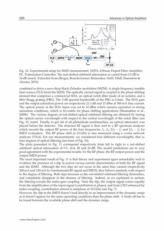
f1
f2
MZMTLS EDFAn0
f1
f2
SOA
Ibias
ONF
FBG
PC
RF-SA
Fig. 10. Experimental setup for IMD3 measurement. EDFA, Erbium-Doped Fiber Amplifier;PC, Polarization Controller. The red-shifted sideband attenuation is varied from 0.5 dB to24 dB (inset). Extracted from (Berger, Bourderionnet, Bretenaker, Dolfi, Dúill, Eisenstein &Alouini, 2010).
combined to drive a zero-chirp Mach-Zehnder modulator (MZM). A single frequency tunablelaser source (TLS) feeds the MZM. The optically carried signal is coupled to the phase shiftingelement that comprises a commercial SOA, an optical notch filter made of an isolator, and afiber Bragg grating (FBG). The 3 dB spectral bandwidth of the FBG is 0.2nm. The SOA gainand the output saturation power are respectively 21.3 dB and 15 dBm at 500 mA bias current.The optical power at the SOA input was set to 10 dBm which ensures operation in strongsaturation conditions, which is favorable for phase shifting applications (Shumakher et al.,2009b). The various degrees of red-shifted optical sideband filtering are obtained by tuningthe optical carrier wavelength with respect to the central wavelength of the notch filter (seeFig. 10, inset). Finally, to get rid of all photodiode nonlinearities, an optical attenuator wasplaced before the detector. The detected RF signal is then sent to a RF spectrum analyzerwhich records the output RF power at the four frequencies f1, f2, 2 f2 − f1 and 2 f1 − f2 forIMD3 evaluation. The RF phase shift at 10 GHz is also measured using a vector networkanalyzer (VNA). For our measurements, we considered four different wavelengths, that is,four degrees of optical filtering (see inset of Fig. 10).The plots presented in Fig. 11 correspond respectively from left to right to a red-shiftedsideband optical attenuation of 0.5, 14.4, 20 and 24 dB. The model predictions are in verygood agreement with the experimental results, for the RF phase, the RF output power and theoutput IMD3 power.The most important result of Fig. 11 is that theory and experiment agree remarkably well toevidence the presence of a dip in power-versus-current characteristics of both the RF signaland the IDM3. Although the two dips do not occur at the same bias current (respectively200 mA and 120 mA for fundamental RF signal and IMD3), they behave similarly with respectto the degree of filtering. Both dips decrease as the red-shifted sideband filtering diminishes,and completely disappear in the absence of filtering. Indeed, as we explained in section,the filtering reveals the index-gain coupling. Near the dip, the output signal comes equallyfrom the amplification of the input signal (contribution in phase), and from CPO enhanced byindex-coupling, (contribution almost in antiphase at 10 GHz) (see Fig. 7).However, the dip in the IMD3 doesn’t lead directly to an improvement of the dynamic rangeas it doesn’t appear for the same operating conditions than the phase shift. A trade-off has tobe found between the available phase shift and the dynamic range.
200 Advances in Optical Amplifiers
www.intechopen.com

200 400 600200 400 600200 400 600
SOA bias current (mA)0 200 400 600
−120
−100
−80
−60
−40
−20
RF
pow
er
(dB
m) Fundamental
IMD3
24dB20dB14.4 dB
0
50
100
150
RF
phase s
hift (d
eg)
Redshiftedsideband
suppression0.5 dB
Fig. 11. Top: RF phase shift at 10 GHz versus SOA bias current; Bottom: RF power atfundamental frequency f1 (in blue), and at 2 f2 − f1, (IMD3, in red). From left to right,red-shifted sideband attenuation increases from 0.5 dB to 24 dB. Symbols representexperimental measurements, and solid lines show theoretical calculations. Extracted from(Berger, Bourderionnet, Bretenaker, Dolfi, Dúill, Eisenstein & Alouini, 2010).
Fig. 12. In blue: Spurious Free Dynamic Range (SFDR); in green: available phase shift. Bothare represented with respect to the red sideband attenuation. The model prediction isrepresented by a line, the dots are the experimental points.
201Slow and Fast Light in Semiconductor Optical Amplifiers for Microwave Photonics Applications
www.intechopen.com

5.2 Influence of the optical filtering on the performance of the phase shifter
To this aim, we compute the Spurious-Free Dynamic Range (SFDR), which is the key figure ofthe dynamic range in microwave photonics (Ackerman, 1994). It is defined as the RF powerrange where the intermodulation products IMD3 are below the noise floor. We represent inFig. 12 the SFDR and the available phase shift with respect to the red sideband attenuation.It appears that the best trade-off between the dynamic range and the available phase shiftcorresponds to the minimum strength of filtering which enables to reveal the index-gaincoupling. With this non-optimized link, we reach a SFDR of 90dB/Hz2/3 for an availablephase shift of 100 degrees.
5.3 Linearized amplification at high frequency
In a more general context, a SOA can be used to reduces the non-linearities of a microwavephotonics link. Indeed, the input linearities (from the modulator for example) can be reducedby the nonlinearities generated by the gain in antiphase created by the CPO. It has alreadybeen demonstrated using a single SOA (without optical filter) at low frequency (2 GHz) (Jeonet al., 2002)). However with a single SOA, the gain in antiphase due to CPO is created onlyat low frequency (below a few GHz), as it is illustrated on Fig. 5. However, when the SOAis followed by an optical filter attenuating the red-shifted sideband, the gain in antiphaseis created at high frequency, as it is illustrated on Fig. 7. This architecture enables then alinearization of the microwave photonics link well beyond the inverse of the carrier lifetime.Indeed we have experimentally demonstrated that a dip in the IMD3 occurs at 10 GHz(Fig. 11). However the instantaneous bandwidth is still limited to the GHz range.
6. Conclusion
We have reviewed the different set-ups proposed in literature, and we have given the physicalinterpretation of each architecture, aiming at helping the reader to understand the underlyingphysical mechanisms.Moreover, we have shown that a robust and predictive model can be derived in order tosimulate and understand the RF transfer function, the generation of spurious signals throughharmonic distortion and intermodulation products, and the intensity noise at the output ofa SOA. This model takes into account the dynamic saturation along the propagation in theSOA, which can be fully characterized by a simple measurement, and only relies on materialfitting parameters, independent of the optical intensity and the injected current. In theseconditions, the model is found to be predictive and can be used to simulate commercial SOAsas well. Moreover, we have presented a generalization of the previous model, which permitsto describe harmonic generation and intermodulation distortions in SOAs. This model usesa rigorous expression of the gain harmonics. Lastly, we showed the possibility to use thisgeneralized model of the RF transfer function to describe the intensity noise at the output ofthe SOA.This useful tool enables to optimize a microwave photonics link including a SOA, by findingthe best operating conditions according to the application. To illustrate this point, the modelis used to find out the guidelines for improving the MWP link dynamic range using a SOAfollowed by an optical filter, in two cases: first, for phase shifting applications, we have shownthat the best trade-off between the dynamic range and the available phase shift correspondsto the minimum strength of filtering which enables to reveal the index-gain coupling. Second,we have experimentally demonstrated and have theoretically explained how an architecture
202 Advances in Optical Amplifiers
www.intechopen.com
composed of a SOA followed by an optical filter can reduce the non-linearities of themodulator, at high frequency, namely beyond the inverse of the carrier lifetime.
7. References
Ackerman, E. (1994). Photonic Aspects of modern radar, Artech House.Agrawal, G. P. (1988). Population pulsations and nondegenerate four-wave mixing in
semiconductor lasers and amplifiers, J. Opt. Soc. Am. B 5(1): 147–159.Agrawal, G. P. & Dutta, N. K. (1993). Semiconductor Lasers, Kluwer Academic, Boston.Anton, M. A., Carreno, F., Calderon, O. G., Melle, S. & Arrieta-Yanez, F. (2009).
Phase-controlled slow and fast light in current-modulated SOA, Journal of PhysicsB: Atomic, Molecular and Optical Physics 42(9): 095403 (8pp).
Berger, P., Alouini, M., Bourderionnet, J., Bretenaker, F. & Dolfi, D. (2009a). Influenceof slow light effect in semiconductor amplifiers on the dynamic range ofmicrowave-photonics links, Slow and Fast Light, Optical Society of America, p. SMB6.
Berger, P., Alouini, M., Bourderionnet, J., Bretenaker, F. & Dolfi, D. (2009b). Slow light usingsemiconductor optical amplifiers: Model and noise characteristics, C. R. Physique10: 991–999.
Berger, P., Alouini, M., Bourderionnet, J., Bretenaker, F. & Dolfi, D. (2010). Dynamic saturationin semiconductoroptical amplifiers: accurate model, roleof carrier density, and slowlight, Opt. Express 18(2): 685–693.
Berger, P., Bourderionnet, J., Alouini, M., Bretenaker, F. & Dolfi, D. (2009). Theoretical studyof the spurious-free dynamic range of a tunable delay line based on slow light in soa,Opt. Express 17(22): 20584–20597.
Berger, P., Bourderionnet, J., Bretenaker, F., Dolfi, D., Dúill, S. O., Eisenstein, G. & Alouini, M.(2010). Intermodulation distortion in microwave phase shifters based on slow andfast light propagation in SOA, Opt. Lett. 35(16): 2762–2764.
Berger, P., Bourderionnet, J., de Valicourt, G., Brenot, R., Dolfi, D., Bretenaker, F. & Alouini,M. (2010). Experimental demonstration of enhanced slow and fast light by forcedcoherent population oscillations in a semiconductor optical amplifier, Opt. Lett.35: 2457.
Bogatov, A. P., Eliseev, P. G. & Sverdlov, B. N. (1975). Anomalous interaction of spectral modesin a semiconductor laser, Quantum Electronics, IEEE Journal of 11: 510.
Boula-Picard, R., Alouini, M., Lopez, J., Vodjdani, N. & Simon, J.-C. (2005). Impact of the gainsaturation dynamics in semiconductor optical amplifiers on the characteristics of ananalog optical link,
Capmany, J., Sales, S., Pastor, D. & Ortega, B. (2002). Optical mixing of microwave signals ina nonlinear semiconductor laser amplifier modulator, Opt. Express 10(3): 183–189.
Dúill, S. O., Shumakher, E. & Eisenstein, G. (2010a). The role of optical filtering in microwavephase shifting, Opt. Lett. 35(13): 2278–2280.
Duill, S., Shumakher, E. & Eisenstein, G. (2010b). Noise properties of microwave phase shiftersbased on SOA, Lightwave Technology, Journal of 28(5): 791 –797.
Henry, C. (1982). Theory of the linewidth of semiconductor lasers, Quantum Electronics, IEEEJournal of 18(2): 259 – 264.
Jeon, D.-H., Jung, H.-D. & Han, S.-K. (2002). Mitigation of dispersion-induced effects using soain analog optical transmission, Photonics Technology Letters, IEEE 14(8): 1166 – 1168.
203Slow and Fast Light in Semiconductor Optical Amplifiers for Microwave Photonics Applications
www.intechopen.com
Lloret, J., Ramos, F., Sancho, J., Gasulla, I., Sales, S. & Capmany, J. (2010). Noise spectrumcharacterization of slow light soa-based microwave photonic phase shifters, PhotonicsTechnology Letters, IEEE 22(13): 1005 –1007.
Mørk, J., Kjær, R., van der Poel, M. & Yvind, K. (2005). Slow light in a semiconductorwaveguide at gigahertz frequencies, Opt. Express 13(20): 8136–8145.
Olsson, N. (1989). Lightwave systems with optical amplifiers, Lightwave Technology, Journal of7(7): 1071–1082.
Peatross, J., Glasgow, S. A. & Ware, M. (2000). Average energy flow of optical pulses indispersive media, Phys. Rev. Lett. 84(11): 2370–2373.
Pesala, B., Chen, Z., Uskov, A. V. & Chang-Hasnain, C. (2006). Experimental demonstrationof slow and superluminal light in semiconductor optical amplifiers, Opt. Express14(26): 12968–12975.
Shumakher, E., Duill, S. & Eisenstein, G. (2009a). Optoelectronic oscillator tunable by an soabased slow light element, Lightwave Technology, Journal of 27(18): 4063–4068.
Shumakher, E., Dúill, S. O. & Eisenstein, G. (2009b). Signal-to-noise ratio of a semiconductoroptical-amplifier-based optical phase shifter, Opt. Lett. 34(13): 1940–1942.
Su, H. & Chuang, S. L. (2006). Room temperature slow and fast light in quantum-dotsemiconductor optical amplifiers, Applied Physics Letters 88(6): 061102.
Xue, W., Chen, Y., Öhman, F., Sales, S. & Mørk, J. (2008). Enhancing light slow-down insemiconductor optical amplifiers by optical filtering, Opt. Lett. 33(10): 1084–1086.
Xue, W., Sales, S., Capmany, J. & Mørk, J. (2009). Experimental demonstration of 360otunablerf phase shift using slow and fast light effects, Slow and Fast Light, Optical Society ofAmerica, p. SMB6.
Xue, W., Sales, S., Mork, J. & Capmany, J. (2009). Widely tunable microwave photonicnotch filter based on slow and fast light effects, Photonics Technology Letters, IEEE21(3): 167–169.
204 Advances in Optical Amplifiers
www.intechopen.com

Advances in Optical AmplifiersEdited by Prof. Paul Urquhart
ISBN 978-953-307-186-2Hard cover, 436 pagesPublisher InTechPublished online 14, February, 2011Published in print edition February, 2011
InTech EuropeUniversity Campus STeP Ri Slavka Krautzeka 83/A 51000 Rijeka, Croatia Phone: +385 (51) 770 447 Fax: +385 (51) 686 166www.intechopen.com
InTech ChinaUnit 405, Office Block, Hotel Equatorial Shanghai No.65, Yan An Road (West), Shanghai, 200040, China
Phone: +86-21-62489820 Fax: +86-21-62489821
Optical amplifiers play a central role in all categories of fibre communications systems and networks. Bycompensating for the losses exerted by the transmission medium and the components through which thesignals pass, they reduce the need for expensive and slow optical-electrical-optical conversion. The photonicgain media, which are normally based on glass- or semiconductor-based waveguides, can amplify many highspeed wavelength division multiplexed channels simultaneously. Recent research has also concentrated onwavelength conversion, switching, demultiplexing in the time domain and other enhanced functions. Advancesin Optical Amplifiers presents up to date results on amplifier performance, along with explanations of theirrelevance, from leading researchers in the field. Its chapters cover amplifiers based on rare earth doped fibresand waveguides, stimulated Raman scattering, nonlinear parametric processes and semiconductor media.Wavelength conversion and other enhanced signal processing functions are also considered in depth. Thisbook is targeted at research, development and design engineers from teams in manufacturing industry,academia and telecommunications service operators.
How to referenceIn order to correctly reference this scholarly work, feel free to copy and paste the following:
Perrine Berger, Jérôme Bourderionnet, Daniel Dolfi, Fabien Bretenaker and Mehdi Alouini (2011). Slow andFast Light in Semiconductor Optical Amplifiers for Microwave Photonics Applications, Advances in OpticalAmplifiers, Prof. Paul Urquhart (Ed.), ISBN: 978-953-307-186-2, InTech, Available from:http://www.intechopen.com/books/advances-in-optical-amplifiers/slow-and-fast-light-in-semiconductor-optical-amplifiers-for-microwave-photonics-applications