ELTR 130 (Operational Amplifiers 1), section 1 · PDF fileELTR 130 (Operational Amplifiers...
117
ELTR 130 (Operational Amplifiers 1), section 1 Recommended schedule Day 1 Topics: Differential pair circuits Questions: 1 through 15 Lab Exercise: Discrete differential amplifier (question 56) Day 2 Topics: The basic operational amplifier Questions: 16 through 25 Lab Exercise: Discrete differential amplifier (question 56, continued) Day 3 Topics: Using the operational amplifier as a comparator Questions: 26 through 35 Lab Exercise: Comparator circuit (question 57) Day 4 Topics: Using the operational amplifier as a voltage buffer Questions: 36 through 45 Lab Exercise: Opamp voltage follower (question 58) Day 5 Topics: Additional applications of feedback (optional) Questions: 46 through 55 Lab Exercise: Linear voltage regulator circuit (question 59) Day 6 Exam 1: includes Comparator circuit performance assessment Lab Exercise: Select an opamp project to prototype and troubleshoot by the end of the next course section (ELTR130, Section 2) Troubleshooting practice problems Questions: 62 through 71 General concept practice and challenge problems Questions: 72 through the end of the worksheet Impending deadlines Troubleshooting assessment (project prototype) due at end of ELTR130, Section 2 Question 60: Troubleshooting log Question 61: Sample troubleshooting assessment grading criteria 1
Transcript of ELTR 130 (Operational Amplifiers 1), section 1 · PDF fileELTR 130 (Operational Amplifiers...

ELTR 130 (Operational Amplifiers 1), section 1
Recommended schedule
Day 1Topics: Differential pair circuitsQuestions: 1 through 15Lab Exercise: Discrete differential amplifier (question 56)
Day 2Topics: The basic operational amplifierQuestions: 16 through 25Lab Exercise: Discrete differential amplifier (question 56, continued)
Day 3Topics: Using the operational amplifier as a comparatorQuestions: 26 through 35Lab Exercise: Comparator circuit (question 57)
Day 4Topics: Using the operational amplifier as a voltage bufferQuestions: 36 through 45Lab Exercise: Opamp voltage follower (question 58)
Day 5Topics: Additional applications of feedback (optional)Questions: 46 through 55Lab Exercise: Linear voltage regulator circuit (question 59)
Day 6Exam 1: includes Comparator circuit performance assessmentLab Exercise: Select an opamp project to prototype and troubleshoot by the end of the next course
section (ELTR130, Section 2)
Troubleshooting practice problemsQuestions: 62 through 71
General concept practice and challenge problemsQuestions: 72 through the end of the worksheet
Impending deadlinesTroubleshooting assessment (project prototype) due at end of ELTR130, Section 2Question 60: Troubleshooting logQuestion 61: Sample troubleshooting assessment grading criteria
1

ELTR 130 (Operational Amplifiers 1), section 1
Project ideas
Audio signal generator amplifier: Uses an op-amp to amplify the output of a digital audio playback device(such as a CD-audio or MP3 player) for use as a sine wave signal generator. Sine waves at different frequenciesare recorded on digital media as different tracks – the op-amp circuit providing voltage and current gain– allowing the use of any inexpensive consumer-grade audio playback device as an audio frequency signalgenerator.
Intercom system: Uses an op-amp to amplify the output of a speaker (used as a microphone) to poweranother speaker located some distance away. With a reversing switch, the roles of the two speakers may bereversed (send versus receive).
Seismograph: Uses an op-amp to amplify small voltages generated by a stationary ”pickup” coil located neara pendulum-mounted permanent magnet. Vibrations in the earth create motion between the magnet andthe coil, inducing voltage in the coil. The op-amp output then drives a meter, recording device, or an alarm.
Pulse-width modulation signal generator: There are many ways to make such a circuit, but almost all ofthem use a comparator to compare an adjustable DC reference voltage against a varying (oscillating) voltageproduced by an oscillator circuit. The resulting comparator output will be a square wave with variable dutycycle, useful for driving power transistors for PWM power control of electric loads.
Series voltage regulator: Uses an op-amp to ”buffer” the reference voltage of a zener diode, driving a transistorto maintain constant DC voltage to a load. The op-amp provides much greater precision and regulation overa wide range of load resistances than a simple zener-BJT regulator circuit could on its own.
Amplified audio detector: The ”sensitive audio detector” circuit suggested in ELTR115 (AC 2) may beimproved with the addition of an op-amp amplification stage. This can drastically raise input impedanceand sensitivity.
Infra-red motion sensor: Passive infra-red detectors are available for purchase (or salvaged from old motion-sensitive light controller circuits) which output a small DC voltage corresponding to IR light intensity. Byamplifying this voltage and passing it through an active differentiator circuit, an output voltage representingrate of change of IR light will be produced. This signal may then be sent to a comparator to trigger analarm or take some other action when a warm object moves by the sensor.
High-impedance analog voltmeter: Uses a JFET or MOSFET input op-amp to drive and analog metermovement for precise measurement of DC voltage.
2

ELTR 130 (Operational Amplifiers 1), section 1
Skill standards addressed by this course section
EIA Raising the Standard; Electronics Technician Skills for Today and Tomorrow, June 1994
E Technical Skills – Analog CircuitsE.10 Understand principles and operations of operational amplifier circuits.E.11 Fabricate and demonstrate operational amplifier circuits.E.12 Troubleshoot and repair operational amplifier circuits.
B Basic and Practical Skills – Communicating on the JobB.01 Use effective written and other communication skills. Met by group discussion and completion of labwork.B.03 Employ appropriate skills for gathering and retaining information. Met by research and preparation
prior to group discussion.B.04 Interpret written, graphic, and oral instructions. Met by completion of labwork.B.06 Use language appropriate to the situation. Met by group discussion and in explaining completed labwork.B.07 Participate in meetings in a positive and constructive manner. Met by group discussion.B.08 Use job-related terminology. Met by group discussion and in explaining completed labwork.B.10 Document work projects, procedures, tests, and equipment failures. Met by project construction and/or
troubleshooting assessments.C Basic and Practical Skills – Solving Problems and Critical Thinking
C.01 Identify the problem. Met by research and preparation prior to group discussion.C.03 Identify available solutions and their impact including evaluating credibility of information, and locating
information. Met by research and preparation prior to group discussion.C.07 Organize personal workloads. Met by daily labwork, preparatory research, and project management.C.08 Participate in brainstorming sessions to generate new ideas and solve problems. Met by group discussion.
D Basic and Practical Skills – ReadingD.01 Read and apply various sources of technical information (e.g. manufacturer literature, codes, and
regulations). Met by research and preparation prior to group discussion.E Basic and Practical Skills – Proficiency in Mathematics
E.01 Determine if a solution is reasonable.E.02 Demonstrate ability to use a simple electronic calculator.E.05 Solve problems and [sic] make applications involving integers, fractions, decimals, percentages, and
ratios using order of operations.E.06 Translate written and/or verbal statements into mathematical expressions.E.09 Read scale on measurement device(s) and make interpolations where appropriate. Met by oscilloscope
usage.E.12 Interpret and use tables, charts, maps, and/or graphs.E.13 Identify patterns, note trends, and/or draw conclusions from tables, charts, maps, and/or graphs.E.15 Simplify and solve algebraic expressions and formulas.E.16 Select and use formulas appropriately.E.17 Understand and use scientific notation.
3

ELTR 130 (Operational Amplifiers 1), section 1
Common areas of confusion for students
Difficult concept: Inverting nature of common-emitter amplifier.Some students find it quite difficult to grasp why the DC output voltage of a common-emitter amplifier
decreases as the DC input voltage level increases. Step-by-step DC analysis of the circuit is the only remedy Ihave found to this conceptual block: getting students to carefully analyze what happens as voltages increaseand decrease.
Difficult concept: Differential pair circuits.Perhaps the most difficult concept to grasp regarding differential pair circuits is that they are basically a
hybrid of common-collector, common-base, and common-emitter amplifiers. This is why a strong knowledgeof the three basic amplifier types is essential for understanding how differential pairs work, and why I beginexploring differential pairs by reviewing C-C, C-E, and C-B amplifiers.
Difficult concept: Determining comparator output polarity.The key to determining the polarity of a comparator’s output is applying Kirchhoff’s Voltage Law to the
two signals at the input terminals to find the differential input voltage, then seeing whether the differentialvoltage’s polarity matches the polarity markings of the comparator’s input terminals. If so, the output willsaturate in a positive direction. If not, the output will saturate in a negative direction.
Difficult concept: Negative feedback.Few concepts are as fundamentally important in electronics as negative feedback, and so it is essential
for the electronics student to learn well. However, it is not an easy concept for many to grasp. The notionthat a portion of the output signal may be ”fed back” into the input in a degenerative manner to stabilizegain is far from obvious. One of the most powerfully illustrative examples I know of is the use of negativefeedback in a voltage regulator circuit to compensate for the base-emitter voltage drop of 0.7 volts (seequestion file #02286).
Common mistake: Thinking that an opamp’s output current is supplied through its input terminals.This is a misconception that seems to have an amazing resistance to correction. There seem to always
be a few students who think that there is a direct path for current from the input terminals of an opampto its output terminal. It is very important to realize that for most practical purposes, an opamp drawsnegligible current through its input terminals! What current does go through the output terminal is alwayssupplied by the power terminals and from the power supply, never by the input signal(s). To put this intocolloquial terms, the input terminals on an opamp tell the output what to do, but they do not give theoutput its ”muscle” (current) to do it.
I think the reason for this misconception is the fact that power terminals are often omitted from opampsymbols for brevity, and after a while of seeing this it is easy to forget they are really still there performinga useful function!
4

Questions
Question 1
Identify the type of transistor amplifier this is (common-collector, common-emitter, or common-base),and identify whether it is inverting or noninverting.
-V
Vin
Vout
RC
RE
Also, explain how to derive the voltage gain equation for this amplifier:
AV =RC
RE + r′e
file 00882
5

Question 2
Identify the type of transistor amplifier this is (common-collector, common-emitter, or common-base),and identify whether it is inverting or noninverting.
-V
Vin
Vout
RC
RE
Also, explain how to derive the voltage gain equation for this amplifier:
AV =RE
RE + r′e
file 00883
6

Question 3
Identify the type of transistor amplifier this is (common-collector, common-emitter, or common-base),and identify whether it is inverting or noninverting.
-V
RC
RE
Vout
Vin
Also, explain how to derive the voltage gain equation for this amplifier:
AV =RC
r′e
file 03920
7

Question 4
Here, a differential pair circuit is driven by an input voltage at the base of Q2, while the output is takenat the collector of Q2. Meanwhile, the other input (Q1 base) is connected to ground:
+V
Q1 Q2
Vout
Vin
-V
RC RC
RE
Identify what types of amplifier circuits the two transistors are functioning as (common-collector,common-emitter, common-base) when the differential pair is used like this, and write an equation describingthe circuit’s voltage gain. Here is another schematic, showing the transistors modeled as controlled currentsources, to help you with the equation:
+V
Q1 Q2
Vout
Vin
-V
RE
r’e r’e
RC RC
file 03921
8

Question 5
Here, a differential pair circuit is driven by an input voltage at the base of Q1, while the output is takenat the collector of Q2. Meanwhile, the other input (Q2 base) is connected to ground:
+V
Q1 Q2
Vout
Vin
-V
RC RC
RE
Identify what types of amplifier circuits the two transistors are functioning as (common-collector,common-emitter, common-base) when the differential pair is used like this, and write an equation describingthe circuit’s voltage gain. Here is another schematic, showing the transistors modeled as controlled currentsources, to help you with the equation:
+V
Q1 Q2
Vout
Vin
-V
RE
r’e r’e
RC RC
file 03922
9

Question 6
Write an approximate equation describing the differential voltage gain for a differential pair circuit suchas this, in terms of the component values:
+V
Q1 Q2
Vout
-V
RC RC
RE
Vin(-)Vin(+)
file 03923
10

Question 7
Describe what happens to each of the output voltages (Vout1 and Vout2) as the input voltage (Vin)decreases:
+V
Q1 Q2
Vin
-V
Vout2Vout1
file 01242
11

Question 8
Suppose this differential-pair circuit was perfectly balanced. In this condition, how much voltage wouldbe expected between the two transistors’ collector terminals?
+V
Q1 Q2
-V
Vdiff
What would happen to this differential voltage (Vdiff ) if transistor Q2 were to increase in temperature,while transistor Q1 remained at the same temperature? Explain your answer.
file 00887
Question 9
What is common-mode voltage, and how should a differential amplifier (ideally) respond to it?file 00939
12

Question 10
If we connect the two transistor bases together in a differential pair circuit, it can only see common-modeinput voltage (no differential input voltage):
+V
Q1 Q2
Vout
-V
RC RC
RE
Vin(CM)
An important performance parameter of any differential amplifier is its common-mode voltage gain.Ideally, a differential-input amplifier should ignore any and all common-mode voltage, but in reality there isalways some amplification of common-mode voltage. We need to figure out how much of that there will bein any differential-pair circuit.
To help us analyze this circuit (with both inputs tied together so it only sees common-mode inputvoltage), I will re-draw it in such a way that reflects the symmetrical nature of the circuit:
+V
Q1 Q2
Vout
-V
RC RC
Vin(CM)
-V
2RE2RE
13

First, explain why this re-drawing is justified, and then write the equation describing the common-modevoltage gain of this circuit, in terms of the component values.
file 03924
Question 11
Common-mode rejection ratio is the ratio between a differential amplifier’s differential voltage gain andits common-mode voltage gain:
CMRR =AV (diff)
AV (CM)
The greater this parameter’s value, the better the differential amplifier will perform as a truly differentialamplifier. Combine the equations for differential voltage gain and for common-mode voltage gain for thefollowing differential amplifier circuit, into a single equation for CMRR:
+V
Q1 Q2
Vout
-V
RC RC
RE
Vin(-)Vin(+)
file 03925
14

Question 12
An interesting technique to achieve extremely high voltage gain from a single-stage transistor amplifieris to substitute an active load for the customary load resistor (located at the collector terminal):
Vin
Vout
RE
RC (passive load)
Vin
Vout
RE
(active load)
+V +V
Usually, this ”active load” takes the form of a current mirror circuit, behaving as a current regulatorrather than as a true current source.
Explain why the presence of an active load results in significantly more voltage gain than a plain(passive) resistor. If the active load were a perfect current regulator, holding collector current absolutelyconstant despite any change in collector-base conductivity for the main amplifying transistor, what wouldthe voltage gain be?
file 02657
15

Question 13
An improvement to the resistor-based differential amplifier design is the addition of a constant-currentsource where the two transistors’ emitter currents mesh together:
+V
Q1 Q2
-V
Vout
What does the constant-current source ”look like” to the rest of the amplifier, in terms of equivalentresistance? What advantage does this give to the amplifier’s performance, over the (simpler) resistor design?Finally, how is this constant-current source actually constructed in a typical differential amplifier circuit?
file 00936
16

Question 14
Differential amplifiers often make use of active loads: a current mirror circuit to establish collectorcurrents between the two transistors, rather than load resistors.
+V
Q1 Q2
-V
Vout
Current mirror
What does the current mirror ”look like” to the common-emitter side of the differential amplifiercircuit, when we apply the Superposition theorem? What aspect of the differential amplifier’s performanceis primarily enhanced with the addition of the current mirror to the circuit?
file 00937
17
Question 15
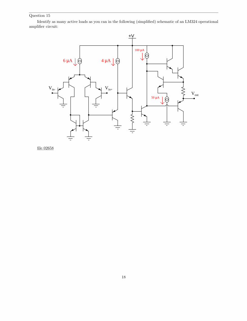
Identify as many active loads as you can in the following (simplified) schematic of an LM324 operationalamplifier circuit:
6 µA 4 µA
100 µA
50 µAVout
+V
Vin+Vin-
file 02658
18

Question 16
Many op-amp circuits require a dual or split power supply, consisting of three power terminals: +V,-V, and Ground. Draw the necessary connections between the 6-volt batteries in this schematic diagram toprovide +12 V, -12 V, and Ground to this op-amp:
−
+
+12 V
-12 V
6 volts each
Load
file 00880
Question 17
The 8-pin Dual-Inline-Package (DIP) is a common format in which single and dual operational amplifiersare housed. Shown here are the case outlines for two 8-pin DIPs. Draw the internal op-amp connections fora single op-amp unit, and for a dual op-amp unit:
8 7 6
1 2 3 4
5 8 7 6
1 2 3 4
5
Single op-amp Dual op-amp
You will need to research some op-amp datasheets to find this information. Examples of single op-ampchips include the LM741, CA3130, and TL081. Examples of dual op-amp chips include the LM1458 andTL082.
file 00874
19

Question 18
Shown here is a simplified schematic diagram of one of the operational amplifiers inside a TL08x (TL081,TL082, or TL084) op-amp integrated circuit:
Vout
+V
Vin+Vin-
-V
Qualitatively determine what will happen to the output voltage (Vout) if the voltage on the noninvertinginput (Vin+) increases, and the voltage on the inverting input (Vin−) remains the same (all voltages arepositive quantities, referenced to -V). Explain what happens at every stage of the op-amp circuit (voltagesincreasing or decreasing, currents increasing or decreasing) with this change in input voltage.
file 00800
20

Question 19
Shown here is a simplified schematic diagram of one of the operational amplifiers inside an LM324 quadop-amp integrated circuit:
6 µA 4 µA
100 µA
50 µAVout
+V
Vin+Vin-
Qualitatively determine what will happen to the output voltage (Vout) if the voltage on the invertinginput (Vin−) increases, and the voltage on the noninverting input (Vin+) remains the same (all voltagesare positive quantities, referenced to ground). Explain what happens at every stage of the op-amp circuit(voltages increasing or decreasing, currents increasing or decreasing) with this change in input voltage.
file 00799
Question 20
Ideally, what should the output voltage of an op-amp do if the noninverting voltage is greater (morepositive) than the inverting voltage?
−
+
+V
-V
+
- +
-
???
file 00802
21

Question 21
An operational amplifier is a particular type of differential amplifier. Most op-amps receive two inputvoltage signals and output one voltage signal:
−
+
Vin1
Vin2
Vout
+ power
- power
Here is a single op-amp, shown under two different conditions (different input voltages). Determine thevoltage gain of this op-amp, given the conditions shown:
−
+
+12 V
-12 V
+12 V
+12 VVout = 1.5 V
Vin1 = 1.00 V
Vin2 = 1.00003 V
−
+
+12 V
-12 V
+12 V
+12 VVout = 6.8 V
Vin1 = 1.00 V
Vin2 = 1.00004 V
Also, write a mathematical formula solving for differential voltage gain (AV ) in terms of an op-amp’sinput and output voltages.
file 00848
22

Question 22
Ideally, when the two input terminals of an op-amp are shorted together (creating a condition of zerodifferential voltage), and those two inputs are connected directly to ground (creating a condition of zerocommon-mode voltage), what should this op-amp’s output voltage be?
− +
Vout = ???
+15 V -15 V
In reality, the output voltage of an op-amp under these conditions is not the same as what would beideally predicted. Identify the fundamental problem in real op-amps, and also identify the best solution.
file 00847
Question 23
What does it mean if an operational amplifier has the ability to ”swing its output rail to rail”? Why isthis an important feature to us?
file 00844
Question 24
A very important parameter of operational amplifier performance is slew rate. Describe what ”slewrate” is, and why it is important for us to consider in choosing an op-amp for a particular application.
file 00846
Question 25
Some precision operational amplifiers are programmable. What does this feature mean? In what waycan you ”program” an op-amp?
file 00845
23
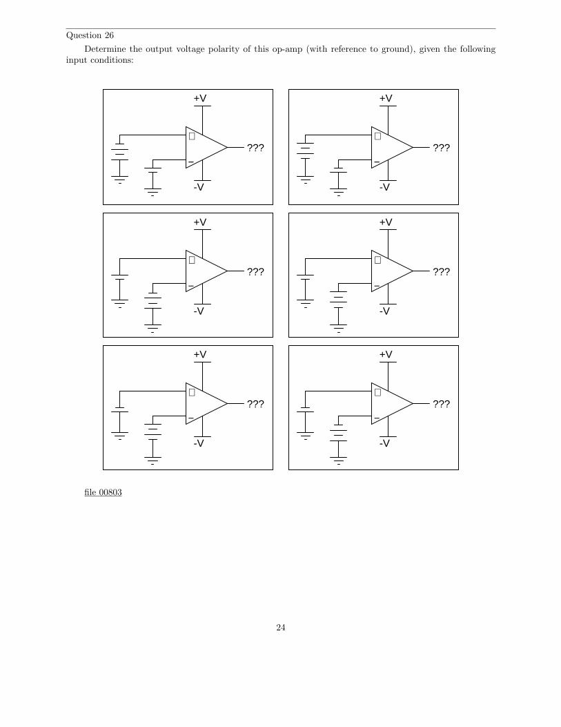
Question 26
Determine the output voltage polarity of this op-amp (with reference to ground), given the followinginput conditions:
−
+
+V
-V
???−
+
+V
-V
???
−
+
+V
-V
???−
+
+V
-V
???
−
+
+V
-V
???−
+
+V
-V
???
file 00803
24

Question 27
Although the following symbol is generally interpreted as an operational amplifier (”op-amp”), it mayalso be used to represent a comparator:
−
+
What is the difference between a comparator such as the model LM319, and a true operational amplifiersuch as the model LM324? Are the two devices interchangeable, or is there any significant difference despitethe exact same schematic symbols? Explain your answer.
file 00875
Question 28
In this circuit, a solar cell converts light into voltage for the opamp to ”read” on its noninverting input.The opamp’s inverting input connects to the wiper of a potentiometer. Under what conditions does the LEDenergize?
−+
+V
LED
+V
file 00872
Question 29
What does the phrase open-loop voltage gain mean with reference to an operational amplifier? For atypical opamp, this gain figure is extremely high. Why is it important that the open-loop voltage gain behigh when using an opamp as a comparator?
file 00873
25

Question 30
A student is operating a simple comparator circuit and documenting the results in a table:
Vin(+)Vin(-)
V Ω
COMA
Vout
V Ω
COMA
V Ω
COMA
6 V
6 V
Vin(+) Vin(−) Vout
3.00 V 1.45 V 10.5 V3.00 V 2.85 V 10.4 V3.00 V 3.10 V 1.19 V3.00 V 6.75 V 1.20 V
Vin(+) Vin(−) Vout
2.36 V 6.50 V 1.20 V4.97 V 6.50 V 1.21 V7.05 V 6.50 V 10.5 V9.28 V 6.50 V 10.4 V
Vin(+) Vin(−) Vout
10.4 V 9.87 V 10.6 V1.75 V 1.03 V 10.5 V0.31 V 1.03 V 10.5 V5.50 5.65 V 1.19 V
One of these output voltage readings is anomalous. In other words, it does not appear to be ”correct”.This is very strange, because these figures are real measurements and not predictions! Perplexed, the studentapproaches the instructor and asks for help. The instructor sees the anomalous voltage reading and says twowords: latch-up. With that, the student goes back to research what this phrase means, and what it has todo with the weird output voltage reading.
Identify which of these output voltage measurements is anomalous, and explain what ”latch-up” has todo with it.
file 00876
26

Question 31
In this circuit, an op-amp turns on an LED if the proper input voltage conditions are met:
−
+
+V
+V
+V
+V
Power supply
Trace the complete path of current powering the LED. Where, exactly, does the LED get its powerfrom?
file 00801
Question 32
Explain the operation of this sound-activated relay circuit:
−
+
Microphone
+V+V
Relay+V
-V
file 00879
27

Question 33
In this automatic cooling fan circuit, a comparator is used to turn a DC motor on and off when thesensed temperature reaches the ”setpoint” established by the potentiometer:
6 V
6 V
+to
Thermistor
Mtr
741
The circuit works just as it is supposed to in turning the motor on and off, but it has a strange problem:the transistor gets warm when the motor is off! Oddly enough, the transistor actually cools down when themotor turns on.
Describe what you would measure first in troubleshooting this problem. Based on the particular modelof op-amp used (a model LM741C), what do you suspect is the problem here?
file 00877
28

Question 34
Photovoltaic solar panels produce the most output power when facing directly into sunlight. To maintainproper positioning, ”tracker” systems may be used to orient the panels’ direction as the sun ”moves” fromeast to west across the sky:
(Sun)
Solar panelAxis of rotation
Axis of rotation
One way to detect the sun’s position relative to the panel is to attach a pair of Light-Dependent Resistors(LDR’s) to the solar panel in such a way that each LDR will receive an equal amount of light only if thepanel is pointed directly at the sun:
(Sun)
Photoresistors
Two comparators are used to sense the differential resistance produced by these two LDR’s, and activatea tracking motor to tilt the solar panel on its axis when the differential resistance becomes too great. An”H-drive” transistor switching circuit takes the comparators’ output signals and amplifies them to drive apermanent-magnet DC motor one way or the other:
29

+12 V+12 V
−
+
−
+
Mtr
Q1 Q2
Q3 Q4
+12 V
LDR1
LDR2
U1
U2
+12 V
100 kΩ
1 kΩ
100 kΩ
1 kΩ
150 Ω
150 Ω
150 Ω150 Ω
In this circuit, what guarantees that the two comparators never output a ”high” (+V) voltagesimultaneously, thus attempting to move the tracking motor clockwise and counter-clockwise at the sametime?
file 00881
30

Question 35
Trace the output waveform of this comparator circuit:
−
+
+V
-V
Vout Vin
0
Vref
Vin
Vref
+V
-V
file 00878
31

Question 36
The voltage gain of a single-ended amplifier is defined as the ratio of output voltage to input voltage:
Vin Vout
Amplifier
AV
AV =Vout
Vin
Often voltage gain is defined more specifically as the ratio of output voltage change to input voltagechange. This is generally known as the AC voltage gain of an amplifier:
AV (AC) =∆Vout
∆Vin
In either case, though, gain is a ratio of a single output voltage to a single input voltage.
How then do we generally define the voltage gain of a differential amplifier, where there are two inputs,not just one?
VoutAV
−
+
Vin(-)
Vin(+)
Differentialamplifier
file 02287
Question 37
Write the transfer function (input/output equation) for an operational amplifier with an open-loopvoltage gain of 100,000. In other words, write an equation describing the output voltage of this op-amp(Vout) for any combination of input voltages (Vin(+) and Vin(−)):
−
+Vin(+)
Vin(-)
Vout
file 00925
32

Question 38
How much voltage would have to be ”dialed up” at the potentiometer in order to stabilize the outputat exactly 0 volts, assuming the opamp has no input offset voltage?
−
+
+12 V
-12 V5 V-12 V
+12 V
???
+V
-Voltmeter
file 00924
Question 39
An op-amp has +3 volts applied to the inverting input and +3.002 volts applied to the noninvertinginput. Its open-loop voltage gain is 220,000. Calculate the output voltage as predicted by the followingformula:
Vout = AV
(
Vin(+) − Vin(−)
)
How much differential voltage (input) is necessary to drive the output of the op-amp to a voltage of -4.5volts?
file 00926
Question 40
Write the transfer function (input/output equation) for an operational amplifier with an open-loopvoltage gain of 100,000, and the inverting input connected directly to its output terminal. In other words,write an equation describing the output voltage of this op-amp (Vout) for any given input voltage at thenoninverting input (Vin(+)):
−
+Vin(+)
Vin(-)
Vout
Then, once you have an equation written, solve for the over-all voltage gain (AV = Vout
Vin(+)) of this
amplifier circuit, and calculate the output voltage for a noninverting input voltage of +6 volts.file 00927
33

Question 41
How much effect will a change in the op-amp’s open-loop voltage gain have on the overall voltage gainof a negative-feedback circuit such as this?
−
+Vout
Vin
If the open-loop gain of this operational amplifier were to change from 100,000 to 200,000, for example,how big of an effect would it have on the voltage gain as measured from the noninverting input to the output?
file 02288
Question 42
For all practical purposes, how much voltage exists between the inverting and noninverting inputterminals of an op-amp in a functioning negative-feedback circuit?
file 00930
34

Question 43
A helpful model for understanding opamp function is one where the output of an opamp is thought ofas being the wiper of a potentiometer, the wiper position automatically adjusted according to the differencein voltage measured between the two inputs:
+V
-Voltmeter
Vin(+)
Vin(-)
Vout
+V
-V
Positive powersupply "rail"
supply "rail"Negative power
To elaborate further, imagine an extremely sensitive, analog, zero-center voltmeter inside the opamp,where the moving-coil mechanism of the voltmeter mechanically drives the potentiometer wiper. The wiper’sposition would then be proportional to both the magnitude and polarity of the difference in voltage betweenthe two input terminals.
Realistically, building such a voltmeter/potentiometer mechanism with the same sensitivity and dynamicperformance as a solid-state opamp circuit would be impossible, but the point here is to model the opampin terms of components that we are already very familiar with, not to suggest an alternative constructionfor real opamps.
Describe how this model helps to explain the output voltage limits of an opamp, and also where theopamp sources or sinks load current from.
file 02290
35

Question 44
Complete the table of voltages for this opamp ”voltage follower” circuit:
−
+VoutVin
+15 V
-15 V
Vin Vout
0 volts 0 volts+5 volts+10 volts+15 volts+20 volts-5 volts-10 volts-15 volts-20 volts
file 02289
36

Question 45
A student builds the following regulated AC-DC power supply circuit, but is dissatisfied with itsperformance:
+V
Gnd
Power plug
The voltage regulation is not as good as the student hoped. When loaded, the output voltage ”sags”more than the student wants. When the zener diode’s voltage is measured under the same conditions(unloaded output, versus loaded output), its voltage is noted to sag a bit as well. The student realizes thatpart of the problem here is loading of the zener diode through the transistor. In an effort to improve thevoltage regulation of this circuit, the student inserts an opamp ”voltage follower” circuit between the zenerdiode and the transistor:
+V
Gnd
Power plug
−
+
Now the zener diode is effectively isolated from the loading effects of the transistor, and by extension
37

from the output load as well. The opamp simply takes the zener’s voltage and reproduces it at the transistorbase, delivering as much current to the transistor as necessary without imposing any additional load on thezener diode.
This modification does indeed improve the circuit’s ability to hold a steady output voltage underchanging load conditions, but there is still room for improvement. Another student looks at the modifiedcircuit, and suggests one small change that dramatically improves the voltage regulation:
+V
Gnd
Power plug
−
+
Modified feedback connection
Now the output voltage holds steady at the zener diode’s voltage with almost no ”sag” under load!The second student is pleased with the success, but the first student does not understand why this versionof the circuit functions any better than previous version. How would you explain this circuit’s improvedperformance to the first student? How is an understanding of negative feedback essential to being able tocomprehend the operation of this circuit?
file 02286
Question 46
Amplifier distortion occurs when its gain varies as a function of the instantaneous signal amplitude.That is, some parts of the signal waveform become amplified more than others, and this results in thewaveform taking on a slightly different shape.
All active devices, bipolar junction transistors included, are nonlinear to some extent. This term meansthat their gain varies throughout their operating ranges. During the 1920’s, an electrical engineer namedHarold Black was pondering this problem in the design of telephone system amplifiers. His solution came tohim in a flash of insight one day, as he was commuting from work on a ferry boat. Explain what his solutionto this problem was.
file 01244
Question 47
A very important concept in electronics is that of negative feedback. This is an extremely importantconcept to grasp, as a great many electronic systems exploit this principle for their operation and cannot beproperly understood without a comprehension of it.
However important negative feedback might be, it is not the easiest concept to understand. In fact, it isquite a conceptual leap for some. The following is a list of examples – some electronic, some not – exhibitingnegative feedback:
38

• A voltage regulating circuit• An auto-pilot system for an aircraft or boat• A thermostatic temperature control system (”thermostat”)• Emitter resistor in a BJT amplifier circuit• Lenz’s Law demonstration (magnetic damping of a moving object)• Body temperature of a mammal• Natural regulation of prices in a free market economy (Adam Smith’s ”invisible hand”)• A scientist learning about the behavior of a natural system through experimentation.
For each case, answer the following questions:
• What variable is being stabilized by negative feedback?• How is the feedback taking place (step by step)?• What would the system’s response be like if negative feedback were not present?
file 02253
39

Question 48
A complementary push-pull transistor amplifier built exactly as shown would perform rather poorly,exhibiting crossover distortion:
-V
+V
Vin Vout
crossover distortion
The simplest way to reduce or eliminate this distortion is by adding some bias voltage to each of thetransistors’ inputs, so there will never be a period of time when the two transistors are simultaneously cutoff:
-V
+V
Vin Vout
+V
-V
Vbias
Vbias
no crossoverdistortion!
One problem with this solution is that just a little too much bias voltage will result in overheating of thetransistors, as they simultaneously conduct current near the zero-crossing point of the AC signal. A moresophisticated method of mitigating crossover distortion is to use an opamp with negative feedback, like this:
40

-V
+V
Vin
Vout
no crossoverdistortion!
−
+
Explain how the opamp is able to eliminate crossover distortion in this push-pull amplifier circuit withoutthe need for biasing.
file 02291
41

Question 49
”Split” or ”dual” DC power supplies are essential for powering many types of electronic circuits,especially certain types of operational amplifier circuits. If only a ”single” DC power supply is not available,a ”split” power supply may be roughly simulated through the use of a resistive voltage divider:
"Single" DCpower supply
+V
-V
Ground
R
R
"Split" DCpower supply
The problem with doing this is loading: if more current is drawn from one of the power supply railsthan from the other, the ”split” of voltage will become uneven. The only way that +V and -V will have thesame (absolute) voltage value at the load is if the load impedance is balanced evenly between those rails andground. This scenario is unlikely. Take for instance this example:
"Single" DCpower supply
+V
-V
GroundR
R
Rload1
Rload2
1 kΩ
1 kΩ
150 Ω
2.2 kΩ
24 V
Voltage from +V to Ground = 3.827 V
Voltage from -V to Ground = -20.173 V
A simple opamp circuit, though, can correct this problem and maintain an even ”split” of voltagebetween +V, Ground, and -V:
42

"Single" DCpower supply +V
-V
Ground
R
R
−
+
Explain how this circuit works. What function do the two resistors perform? How is negative feedbackbeing used in this circuit?
file 02293
43

Question 50
The parasitic capacitance naturally existing in two-wire cables can cause problems when connected tohigh-impedance electronic devices. Take for instance certain biomedical probes used to detect electrochemicalevents in living tissue. Such probes may be modeled as voltage sources in series with resistances, thoseresistances usually being rather large due to the probes’ very small surface (contact) areas:
Electrical modelof probe
Vsignal
Rsource
Coaxial cableTo amplifier
circuit
Parasitic capacitanceof cable
When connected to a cable with parasitic capacitance, a low-pass RC filter circuit is formed:
Electrical modelof probe
Vsignal
Rsource To amplifiercircuit
Electrical modelof cable
A low-pass filter is formed . . .
This low-pass filter (or passive integrator, if you wish) is purely unintentional. No one asked for it tobe there, but it is there anyway just due to the natural resistance of the probe and the natural capacitanceof the cable. Ideally, of course, we would like to be able to send the signal voltage (Vsignal) straight to theamplifier with no interference or filtering of any kind so we can see exactly what it is we’re trying to measure.
One clever way of practically eliminating the effects of cable capacitance is to encase the signal wire inits own shield, and then drive that shield with the exact same amount of voltage from a voltage follower atthe other end of the cable. This is called guarding:
Electrical modelof probe
Vsignal
Rsource
To amplifiercircuit
−
+
An equivalent schematic may make this technique more understandable:
44

Electrical modelof probe
Vsignal
Rsource
To amplifiercircuit
Electrical modelof cable
Center conductor
Guard (driven shield)
Outside shield
−
+
Explain why guarding the signal wire effectively eliminates the effects of the cable’s capacitance.Certainly the capacitance is still present, so how can it not have any effect on the weak signal any more?
file 02292
Question 51
One analogy used to explain and contrast negative feedback versus positive feedback is that of a roundstone, placed on either a hilltop or a valley:
Hill
Stone
Stone
Valley
The stability of the stone in each of these scenarios represents the stability of a specific type of electricalfeedback system. Which of these scenarios represents negative feedback, which represents positive feedback,and why?
file 01149
45

Question 52
Determine the ”trip” voltage of this comparator circuit: the value of input voltage at which the opamp’soutput changes state from fully positive to fully negative or visa-versa:
−
+
+12 V
1 kΩ
3.3 kΩ
Vin
Vout
Now, what do you suppose would happen if the output were fed back to the noninverting input througha resistor? You answer merely has to be qualitative, not quantitative:
−
+
+12 V
1 kΩ
3.3 kΩ
Vin
Vout
Rfeedback
For your information, this circuit configuration is often referred to as a Schmitt trigger.file 02294
46

Question 53
A comparator is used as a high wind speed alarm in this circuit, triggering an audio tone to soundwhenever the wind speed exceeds a pre-set alarm point:
−
+
+V+V
Gen
Anemometer
Cable
The circuit works well to warn of high wind speed, but when the wind speed is just near the thresholdlevel, every little gust causes the alarm to briefly sound, then turn off again. What would be better is forthe alarm to sound at a set wind speed, then stay on until the wind speed falls below a substantially lowerthreshold value (example: alarm at 60 km/h, reset at 50 km/h).
An experienced electronics technician decides to add this functionality to the circuit by adding tworesistors:
47

−
+
+V+V
Gen
Anemometer
Cable
Explain why this circuit alteration works to solve the problem.file 01168
Question 54
Assume that the comparator in this circuit is capable of ”swinging” its output fully from rail to rail.Calculate the upper and lower threshold voltages, given the resistor values shown:
−
+
10 kΩ
5 kΩ
+12 V
Vin
-12 V
VUT = VLT =
file 01169
48

Question 55
Assume that the comparator in this circuit is only capable of ”swinging” its output to within 1 volt ofits power supply rail voltages. Calculate the upper and lower threshold voltages, given the resistor valuesshown:
−
+
Vin
2.2 kΩ
+15 V
-15 V6.1 kΩ
VUT = VLT =
file 01170
49

Question 56
Given conditions
Version:
Schematic
Parameters
Predicted Measured
VCC =
VCC
Competency: BJT differential amplifier
Vout
Q1 Q2
Rprg
Q3 Q4
Q5 Q6
Rprg =
IC (Q6)
Which transistor does the inverting input belong to?
Which transistor does the non-inverting input belong to?
R1 R2
R1 = R2 =
Rpot1 Rpot2
Rpot1 = Rpot2 =
file 01997
50

Question 57
Given conditions
Version:
Schematic
Parameters
+V
Predicted Measured
−
+VoutU1
+V =
Vout
Competency: Voltage comparator
Vin(+) = ____ Vin(-) = ____
Vout Vin(+) = ____ Vin(-) = ____
Vout Vin(+) = ____ Vin(-) = ____
Vout Vin(+) = ____ Vin(-) = ____
Rpot1
Rpot2
Rpot1 = Rpot2 =
Fault analysis
Suppose component fails open
shorted
other
What will happen in the circuit?
file 01999
51

Question 58
Given conditions
Version:
Schematic
Parameters
+V
Predicted Measured
or noninverting?
Inverting . . .
Competency: Opamp voltage follower
−
+
-V
VoutU1
+V =
-V =
Vout
Rail-to-rail output swing?
Measured
(Yes/No)
AV (ratio)
AV (dB)
Rpot
Rpot =
TP1
VTP1 =
VTP1 resulting in latch-up
file 01968
52

Question 59
Given conditions
Version:
Schematic
Parameters
Predicted Measured
−
+U1
Competency: Linear voltage regulator circuit
Vsupply
R1
D1
Q1
C1
R1 =
Vzener = C1 =Vsupply (max) =
Vsupply (min) =
Vin(+)
VB (Q1)
PQ1
Calculated
Fault analysis
Suppose component fails open
shorted
other
What will happen in the circuit?
Load
Load =
Vload
file 01998
53

Question 60
Conclusions(i.e. What this tells me . . . )
Troubleshooting log
(i.e. What I did and/or noticed . . . )Actions / Measurements / Observations
file 03933
54

Question 61
NAME: Troubleshooting Grading CriteriaYou will receive the highest score for which all criteria are met.
100 % (Must meet or exceed all criteria listed)A. Absolutely flawless procedureB. No unnecessary actions or measurements taken
90 % (Must meet or exceed these criteria in addition to all criteria for 85% and below)A. No reversals in procedure (i.e. changing mind without sufficient evidence)B. Every single action, measurement, and relevant observation properly documented
80 % (Must meet or exceed these criteria in addition to all criteria for 75% and below)A. No more than one unnecessary action or measurementB. No false conclusions or conceptual errorsC. No missing conclusions (i.e. at least one documented conclusion for action / measurement / observation)
70 % (Must meet or exceed these criteria in addition to all criteria for 65%)A. No more than one false conclusion or conceptual errorB. No more than one conclusion missing (i.e. an action, measurement, or relevant observation without a
corresponding conclusion)
65 % (Must meet or exceed these criteria in addition to all criteria for 60%)A. No more than two false conclusions or conceptual errorsB. No more than two unnecessary actions or measurementsC. No more than one undocumented action, measurement, or relevant observationD. Proper use of all test equipment
60 % (Must meet or exceed these criteria)A. Fault accurately identifiedB. Safe procedures used at all times
50 % (Only applicable where students performed significant development/design work – i.e. not a provencircuit provided with all component values)A. Working prototype circuit built and demonstrated
0 % (If any of the following conditions are true)A. Unsafe procedure(s) used at any point
file 03932
55

Question 62
Predict how the operation of this differential pair circuit will be affected as a result of the followingfaults. Consider each fault independently (i.e. one at a time, no multiple faults):
+V
Q1 Q2
Vout
-V
V1 V2
R1 R2
R3
• Resistor R1 fails open:
• Resistor R2 fails open:
• Resistor R3 fails open:
• Solder bridge (short) across resistor R3:
For each of these conditions, explain why the resulting effects will occur.file 03764
56

Question 63
Predict how the operation of this operational amplifier circuit will be affected as a result of the followingfaults. Specifically, identify whether the output voltage (Vout) will move in a positive direction (closer to the+V rail) or in a negative direction (closer to ground). Consider each fault independently (i.e. one at a time,no multiple faults):
6 µA 4 µA
100 µA
50 µAVout
+V
Vin+Vin-
Q1
Q2 Q3
Q4
Q5 Q6
Q7
Q8
Q9
Q10
Q11
Q12
Q13
R1
R2
I1 I2
I3
I4
• Transistor Q5 fails shorted (collector-to-emitter):
• Transistor Q6 fails shorted (collector-to-emitter):
• Resistor R1 fails open:
• Current source I2 fails shorted:
For each of these conditions, explain why the resulting effects will occur.file 03765
57

Question 64
Predict how the operation of this operational amplifier circuit will be affected as a result of the followingfaults. Specifically, identify whether the output voltage (Vout) will move in a positive direction (closer to the+V rail) or in a negative direction (closer to the -V rail). Consider each fault independently (i.e. one at atime, no multiple faults):
Vout
+V
Vin+Vin-
-V
Q1 Q2
D1
Q3
R1 R2
I1
I2
D2
D3
Q4
Q5
Q6
• Diode D1 fails open:
• Resistor R1 fails shorted:
• Transistor Q2 fails shorted (drain-to-source):
• Transistor Q5 fails shorted (collector-to-emitter):
• Resistor R2 fails open:
• Current source I2 fails open:
For each of these conditions, explain why the resulting effects will occur.file 03766
58

Question 65
Predict how the operation of this sound-activated relay circuit will be affected as a result of the followingfaults. Consider each fault independently (i.e. one at a time, no multiple faults):
−
+
Microphone
+V+V
Relay+V
-V
R1
Rpot
D1
U1
R2 D2
D3
SCR1
• Zener diode D1 fails open:
• Resistor R1 fails open:
• Resistor R2 fails open:
• Microphone voice coil fails open:
• Comparator U1 fails with output saturated positive:
• Diode D3 fails shorted:
For each of these conditions, explain why the resulting effects will occur.file 03767
59

Question 66
Predict how the operation of this thermostat circuit (where the cooling fan motor is supposed to turnon when the temperature gets too high) will be affected as a result of the following faults. Consider eachfault independently (i.e. one at a time, no multiple faults):
+to
Thermistor
Mtr Coolingfan
R1
Rpot
C1
U1
Q1
V1
Cable
• Cable fails open:
• Comparator U1 fails with output saturated positive:
• Resistor R1 fails open:
• Capacitor C1 fails shorted:
• Transistor Q1 fails shorted (drain-to-source):
For each of these conditions, explain why the resulting effects will occur.file 03768
60

Question 67
Predict how the operation of this thermostat circuit (where the cooling fan motor is supposed to turnon when the temperature gets too high) will be affected as a result of the following faults. Consider eachfault independently (i.e. one at a time, no multiple faults):
+to
Thermistor
Mtr Coolingfan
R1
Rpot
C1
U1
Q1
V1
Cable
• Cable fails open:
• Comparator U1 fails with output saturated positive:
• Resistor R1 fails open:
• Cable fails shorted:
• Transistor Q1 fails shorted (drain-to-source):
For each of these conditions, explain why the resulting effects will occur.file 03769
61

Question 68
Predict how the operation of this solar panel tracking circuit (where the tracking motor turns in responseto a difference in light sensed by the two photoresistors) will be affected as a result of the following faults.Assuming that the motor spins clockwise when its left terminal is negative and its right terminal is positive(when Q2 and Q3 are both on), specify the direction of rotation (or non-rotation) resulting from each fault.Consider each fault independently (i.e. one at a time, no multiple faults):
+12 V+12 V
−
+
−
+
Mtr
Q1 Q2
Q3 Q4
+12 V
U1
U2
+12 V
R3
R1
R2
R4
R5
R6
R7
R8
R9 R10
• Photoresistor R1 fails open:
• Photoresistor R2 fails open:
• Resistor R4 fails open:
• Resistor R5 fails open:
• Resistor R7 fails open:
• Resistor R10 fails open:
• Transistor Q3 fails open (collector-to-emitter):
For each of these conditions, explain why the resulting effects will occur.file 03770
62

Question 69
Predict how the operation of this regulated power supply circuit will be affected as a result of thefollowing faults. Consider each fault independently (i.e. one at a time, no multiple faults):
+V
Gnd
Power plug
−
+
T1
Switch
Fuse
D1
D2
D3
D4 C1
R1
U1
Q1
C2
D5
• Transformer T1 primary winding fails open:
• Rectifying diode D3 fails open:
• Rectifying diode D4 fails shorted:
• Resistor R1 fails open:
• Zener diode D5 fails open:
• Operational amplifier U1 fails with output saturated positive:
• Transistor Q1 fails open (collector-to-emitter):
For each of these conditions, explain why the resulting effects will occur.file 03771
63

Question 70
The purpose of this circuit is to provide a pushbutton-adjustable voltage. Pressing one button causesthe output voltage to increase, while pressing the other button causes the output voltage to decrease. Whenneither button is pressed, the voltage remains stable:
+V
−
+
+V
R1
R2
C1
CA3130 Vout
Increase
Decrease
After working just fine for quite a long while, the circuit suddenly fails: now it only outputs zero voltsDC all the time.
An experienced technician first checks the power supply voltage to see if it is within normal limits, andit is. Then, the technician checks the voltage across the capacitor. Explain why this is a good test point tocheck, and what the results of that check would tell the technician about the nature of the fault.
file 03773
64

Question 71
This regulated power supply circuit has a problem. Instead of outputting 15 volts DC (exactly) as itshould, it is outputting 0 volts DC to the load:
−
+U1
Vsupply
R1
D1 Rload
Q1
C1
TP1
TP2
TP3
TP4
You measure 0.25 volts DC between TP4 and ground, and 20 volts between TP1 and ground, using yourvoltmeter. From this information, determine at least two independent faults that could cause this particularproblem.
file 03772
Question 72
Suppose we were to compare the performance of two voltage divider circuits side-by-side. The circuiton the left has one variable resistor (R2), while the circuit on the right has two variable resistors (R1 andR2). The right-hand circuit’s resistors are ganged together in such a way that as one resistance increases,the other will decrease by the same amount, keeping the circuit’s total resistance constant:
R1
R2 Vout
R1
R2 Vout
Rtotal varies Rtotal remains constant
Knowing that the voltage output by a voltage divider is described by the following formula, determinewhich voltage divider circuit yields the greatest change in output voltage for a given change in R2’s resistance.
Vout = Vbattery
(
R2
R1 + R2
)
file 02655
65

Question 73
The purpose of a current mirror circuit is to maintain constant current through a load despite changesin that load’s resistance:
Load
Iconstant
If we were to crudely model the transistor’s behavior as an automatically-varied rheostat – constantlyadjusting resistance as necessary to keep load current constant – how would you describe this rheostat’sresponse to changes in load resistance?
Load
Iconstant
. . .
Rtransistor
In other words, as Rload increases, what does Rtransistor do – increase resistance, decrease resistance,or remain the same resistance it was before? How does the changing value of Rtransistor affect total circuitresistance?
file 02656
66

Question 74
This circuit is part of a weather monitoring station. Wind speed is measured by the voltage outputfrom a permanent-magnet DC generator, turned by a set of vanes. A light bulb lights up when the windspeed passes a threshold (”trip”) value, established by the potentiometer:
Q1 Q2
+V
Gen
Vanes
Based on your understanding of differential pair circuits, is this a high-speed wind indicating circuit ora low-speed wind indicating circuit?
file 00938
67

Question 75
Identify as many active loads as you can in the following schematic of an LM741 operational amplifiercircuit,along with their respective (amplifying) transistors:
Q3 Q4
Q1 Q2
Q5 Q6
R1 R2R3 R4
Q7
Q10
Q8 Q9 Q12
Q11
R5(+) input
(-) input
Q13
offset nulloffset null
+V
-V
Q23
Q16
R9 R8
C1
Q17
Q24
Q22
Q19
Q18
R10
Q15
Q14
R6
OutputR7
Q21
Q20
R11
Internal schematic of a model 741 operational amplifier
file 02659
68

Question 76
One of the first popular operational amplifiers was manufactured by Philbrick Researches, and it wascalled the K2-W. Built with two dual-triode vacuum tubes, its original schematic diagram looked like this:
12AX7
+300 V
220 kΩ
220 kΩ
-300 V
Inverting (-)input
Noninverting (+)input
1 MΩ
2.2 MΩ
510 kΩ
120 kΩ 4.7 MΩ221 kΩ
9.1 kΩ
12AX7
680 kΩ
7.5 pF
500 pF
NE-68
Output
The Philbrick Researches op-amp, model K2-W
To make this opamp circuit easier for modern students to understand, I’ll substitute equivalent solid-state components for all tubes in the original design:
Inverting (-)input
Noninverting (+)input
Output
+V
-V
The Philbrick Researches op-amp, model K2-W, reborn
Q1 Q2 Q3 Q4
69

Explain the configuration (common-source, common-drain, or common-gate) of each transistor in themodernized schematic, identifying the function of each in the operational amplifier circuit.
file 02590
Question 77
Determine the functions for as many components as you can in the following schematic diagram of amodel 741 operational amplifier:
Q3 Q4
Q1 Q2
Q5 Q6
R1 R2R3 R4
Q7
Q10
Q8 Q9 Q12
Q11
R5(+) input
(-) input
Q13
offset nulloffset null
+V
-V
Q23
Q16
R9 R8
C1
Q17
Q24
Q22
Q19
Q18
R10
Q15
Q14
R6
OutputR7
Q21
Q20
R11
Internal schematic of a model 741 operational amplifier
file 02591
70

Question 78
Determine what the magnitude and polarity of the voltmeter’s indication will be in each case:
+-COMA
V
V A
AOFF
6 V
+-
COMA
V
V A
AOFF
6 V
COMA
V
V A
AOFF
+-
COMA
V
V A
AOFF
+-
9 V
+-
6 V
+-
9 V
+-+
-
3 V9 V
5 V
file 03763
71

Question 79
Determine the output voltage polarity of this op-amp (with reference to ground), given the followinginput conditions:
−
+
+V
-V
???
−
+
+V
-V
???
−
+
+V
-V
???−
+
+V
-V
???
−
+
+V
-V
???
−
+
+V
-V
???
file 03761
72
Question 80
Determine the output voltage polarity of this op-amp (with reference to ground), given the followinginput conditions:
−
+
+V
-V
???−
+
+V
-V
???
−
+
+V
-V
???−
+
+V
-V
???
−
+
+V
-V
???
−
+
+V
-V
???
6 V
9 V
8 V
3 V
5 V
2 V
6 V
2 V
6 V
5 V
file 03762
73

Question 81
Just as certain assumptions are often made for bipolar transistors in order to simplify their analysis incircuits (an ideal BJT has negligible base current, IC = IE , constant β, etc.), we often make assumptionsabout operational amplifiers so we may more easily analyze their behavior in closed-loop circuits. Identifysome of these ideal opamp assumptions as they relate to the following parameters:
• Magnitude of input terminal currents:• Input impedance:• Output impedance:• Input voltage range:• Output voltage range:• Differential voltage (between input terminals) with negative feedback:
file 02749
Question 82
Design a passive circuit that will create a ”split” (+V/-V) power supply from a single voltage source:
"Single" DC +V
-V
Ground"Split" DC
power supply
voltage source
???
file 02748
74

Question 83
Ideally, the input terminals of an operational amplifier conduct zero current, allowing us to simplifythe analysis of many opamp circuits. However, in actuality there is a very small amount of current goingthrough each of the input terminals of any opamp with BJT input circuitry. This may cause unexpectedvoltage errors in circuits.
Consider the following voltage buffer circuit:
−
+
Vsource
Rsource
Voltage source tobe buffered
Ibias(+)
Ibias(-)
Vout
Ibias(−) does not cause any trouble for us, because it is completely supplied by the opamp’s output. Theother bias current, though, does cause trouble, because it must go through the source’s Thevenin resistance.When it does, it drops some voltage across that intrinsic source resistance, skewing the amount of voltageactually seen at the noninverting terminal of the opamp.
A common solution to this is to add another resistor to the circuit, like this:
−
+
Vsource
Rsource
Ibias(+)
Ibias(-)
Vout
Vbias(+)
Vbias(-)
Rcomp = Rsource
Explain why the addition of a resistor fixes the problem.file 02462
75

Question 84
This operational amplifier circuit is often referred to as a voltage buffer, because it has unity gain (0dB) and therefore simply reproduces, or ”buffers,” the input voltage:
−
+Vin
Vout
Voltage buffer circuit
Vout = Vin
What possible use is a circuit such as this, which offers no voltage gain or any other form of signalmodification? Wouldn’t a straight piece of wire do the same thing? Explain your answers.
Vin Vout
Vout = Vin
A simpler voltage buffer?
file 03801
76
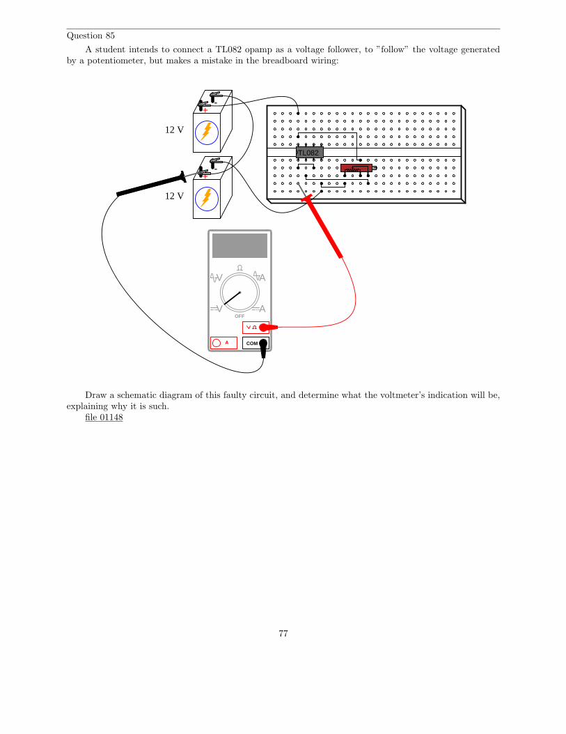
Question 85
A student intends to connect a TL082 opamp as a voltage follower, to ”follow” the voltage generatedby a potentiometer, but makes a mistake in the breadboard wiring:
+-
+-
TL082
12 V
12 V
COMA
V
V A
AOFF
Draw a schematic diagram of this faulty circuit, and determine what the voltmeter’s indication will be,explaining why it is such.
file 01148
77

Question 86
Comparators with positive feedback are sometimes referred to as Schmitt triggers. Suppose you neededa Schmitt trigger for a circuit you were building, but did not have any more integrated circuit comparatorsor op-amps to use. All you have available to you are discrete components. Is there any way you can thinkof to modify the following discrete transistor differential pair so that it behaves as a Schmitt trigger?
+V
file 01243
Question 87
Positive or regenerative feedback is an essential characteristic of all oscillator circuits. Why, then, docomparator circuits utilizing positive feedback not oscillate? Instead of oscillating, the output of a comparatorcircuit with positive feedback simply saturates to one of its two rail voltage values. Explain this.
file 01172
78

Answers
Answer 1
This is a common-emitter amplifier circuit, and it is inverting. Here is a schematic hint for explainingwhy the voltage gain formula is as it is. Note that the transistor is modeled here as a resistance and acontrolled current source:
βib
r’e
B
C
E
-V
RC
RE
Vin
Vout
Follow-up question: the voltage gain equation for this type of transistor amplifier is usually shown in asimpler form that what I provided at the end of the question. Write this simpler form, and explain why itis approximately true.
79

Answer 2
This is a common-collector amplifier circuit, and it is noninverting. Here is a schematic hint for explainingwhy the voltage gain formula is as it is. Note that the transistor is modeled here as a resistance and acontrolled current source:
βib
r’e
B
C
E
-V
RC
Vout
RE
Vin
Follow-up question: the voltage gain equation for this type of transistor amplifier is usually shown in asimpler form that what I provided at the end of the question. Write this simpler form, and explain why itis approximately true.
80

Answer 3
This is a common-base amplifier circuit, and it is noninverting. Here is a schematic hint for explainingwhy the voltage gain formula is as it is. Note that the transistor is modeled here as a resistance and acontrolled current source:
βib
r’e
B
C
E
-V
RC
Vout
RE
Vin
Answer 4
Q2 operates as a common-emitter amplifier, while Q1 does not really act as an amplifier at all (giventhat no input or output connects to it). The gain equation is as such:
AV (invert) =RC
r′e + (r′e||RE)
Follow-up question #1: explain why it is appropriate to simplify the gain equation to this:
AV (invert) ≈RC
2r′e
Follow-up question #2: explain why the simplified gain equation is sometimes written with a negativesign in it:
AV (invert) ≈ −RC
2r′e
81

Answer 5
Q1 operates as a common-collector amplifier, while Q2 acts as a common-base amplifier. The gainequation is as such:
AV (noninvert) =
[
RC
r′e + (r′e||RE)
] [
r′e||RE
r′e
]
Follow-up question: explain why it is appropriate to simplify the gain equation to this:
AV (noninvert) ≈RC
2r′e
Answer 6
AV (diff) =RC
2r′e
Follow-up question: what component value(s) should be altered to maximize differential voltage gain ina differential pair circuit, and why?
Answer 7
Vout1 will decrease (become more negative), while Vout2 will increase (become more positive).
82

Answer 8
In a balanced condition, Vdiff = 0 volts. If Q2 heats up and Q1 does not, a differential voltage willdevelop between the two collector terminals, with Q1’s collector being the positive and Q2’s collector beingthe negative:
+V
Q1 Q2
-V
VdiffQ2 is heated
Follow-up question: what does this phenomenon mean with regard to the stability of differential-pairtransistor circuits under different operating conditions? What might be a good way to maximize circuitstability over a wide range of operating temperatures?
Answer 9
”Common-mode voltage” is the amount of voltage common to both inputs of a differential amplifier.Ideally, a differential amplifier should reject this common-mode voltage, only amplifying the differencebetween the two input voltages.
Follow-up question: what does the phrase common-mode rejection ratio (CMRR) mean for a differentialamplifier?
Answer 10
If the transistors are identical, and receive the same input signal at their base terminals, they will passthe same amount of current from collector to emitter. This means the ”tail” resistor’s current (IRE
) is evenlysplit between the two transistors. With an even split of current, the one resistor will act the same as tworesistors of twice that value, each one carrying only the current of one transistor.
Re-drawn like this, it should be plain to see that the differential pair acts as a swamped common-emitteramplifier, with the common-mode voltage gain described by the following equation:
AV (CM) =RC
r′e + 2RE
Follow-up question: what component value(s) should be altered to minimize common-mode voltage gainin a differential pair circuit, and why?
83
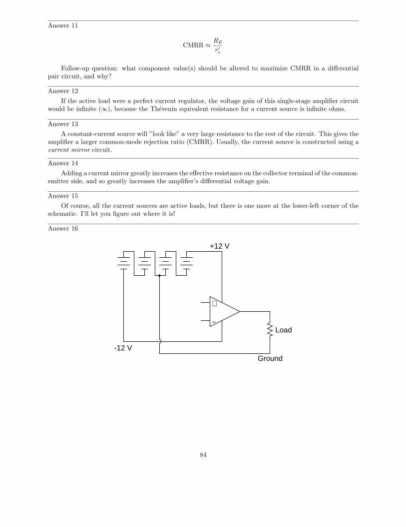
Answer 11
CMRR ≈RE
r′e
Follow-up question: what component value(s) should be altered to maximize CMRR in a differentialpair circuit, and why?
Answer 12
If the active load were a perfect current regulator, the voltage gain of this single-stage amplifier circuitwould be infinite (∞), because the Thevenin equivalent resistance for a current source is infinite ohms.
Answer 13
A constant-current source will ”look like” a very large resistance to the rest of the circuit. This gives theamplifier a larger common-mode rejection ratio (CMRR). Usually, the current source is constructed using acurrent mirror circuit.
Answer 14
Adding a current mirror greatly increases the effective resistance on the collector terminal of the common-emitter side, and so greatly increases the amplifier’s differential voltage gain.
Answer 15
Of course, all the current sources are active loads, but there is one more at the lower-left corner of theschematic. I’ll let you figure out where it is!
Answer 16
−
+
Load
Ground
+12 V
-12 V
84

Answer 17
8 7 6
1 2 3 4
5 8 7 6
1 2 3 4
5
Single op-amp Dual op-amp
− + −
+
+V -V
-V
+V−
+
Answer 18
Here, I’ve labeled a few of the important voltage changes in the circuit, resulting from the increase innoninverting input voltage (Vin+):
Vout
+V
Vin+Vin-
-V
V inc.
V inc.
V dec.
V inc.
V inc.
85

Answer 19
Here, I’ve labeled a few of the important voltage changes in the circuit, resulting from the increase ininverting input voltage (Vin−):
6 µA 4 µA
100 µA
50 µAVout
+V
Vin+Vin-
V inc.
V inc.
V dec.
V dec.
V inc.
Answer 20
In this condition, the output of the op-amp should saturate positive (+V), as if a direct connection weremade inside the op-amp between the output terminal and the +V power supply terminal:
−
+
+V
-V
+
- +
-
(+)
Answer 21
AV = 530,000
AV =∆Vout
∆(Vin2 − Vin1)
Follow-up question: convert this voltage gain figure (as a ratio) into a voltage gain figure in decibels.
86

Answer 22
Ideally, Vout = 0 volts. However, the output voltage of a real op-amp under these conditions willinvariably be ”saturated” at full positive or full negative voltage due to differences in the two branches of its(internal) differential pair input circuitry. To counter this, the op-amp needs to be ”trimmed” by externalcircuitry.
Follow-up question: the amount of differential voltage required to make the output of a real opampsettle at 0 volts is typically referred to as the input offset voltage. Research some typical input offset voltagesfor real operational amplifiers.
Challenge question: identify a model of op-amp that provides extra terminals for this ”trimming”feature, and explain how it works.
Answer 23
Being able to ”swing” the output voltage ”rail to rail” means that the full range of an op-amp’s outputvoltage extends to within millivolts of either power supply ”rail” (+V and -V).
Challenge question: identify at least one op-amp model that has this ability, and at least one that doesnot. Bring the datasheets for these op-amp models with you for reference during discussion time.
Answer 24
”Slew rate” is the maximum rate of voltage change over time (dvdt
) that an op-amp can output.
Answer 25
A ”programmable” op-amp is one with extra connections to its internal circuitry allowing you to setthe current source values using external components.
87

Answer 26
In these illustrations, I have likened the op-amp’s action to that of a single-pole, double-throw switch,showing the ”connection” made between power supply terminals and the output terminal.
−
+
+V
-V
−
+
+V
-V
−
+
+V
-V
−
+
+V
-V
−
+
+V
-V
−
+
+V
-V
(-) (+)
(-)
(-)
(+)
(+)
Answer 27
Comparators are designed for open-loop operation only (no feedback), while operational amplifiers aredesigned to perform well with feedback. For many simple applications, though, a true op-amp does areasonable job as a comparator.
88

Answer 28
The LED energizes under bright-light conditions, de-energizing when the light decreases below thethreshold set by the potentiometer.
Follow-up question: determine what would have to be changed in this circuit to make the LED turn onwhen the solar cell becomes dark.
Answer 29
”Open-loop voltage gain” simply refers to the differential voltage gain of the amplifier, without anyconnections ”feeding back” the amplifier’s output signal to one or more of its inputs. A high gain figuremeans that a very small differential voltage is able to drive the amplifier into saturation.
Answer 30
Latch-up occurs when one of the input voltage signals approaches too close to one of the power supplyrail voltages. The result is the op-amp output saturating ”high” even if it isn’t supposed to.
Challenge question: suppose we expected both input voltages to range between 0 and 10 volts duringnormal operation of this comparator circuit. What could we change in the circuit to allow this range ofoperation and avoid latch-up?
Answer 31
The arrows shown in this diagram trace ”conventional” current flow, not electron flow:
−
+
+V
+V
+V
+V
Power supply
Answer 32
The relay will energize if a loud enough sound is detected by the microphone. The threshold volume isset by the potentiometer.
Follow-up question: how could we equip this circuit with the ability to turn the relay off once it hasbeen turned on?
89

Answer 33
The problem here is that the model 741 op-amp cannot ”swing” its output rail-to-rail. An op-amp withrail-to-rail output voltage capability would not make the transistor heat up in the ”off” mode.
Challenge question: what purpose does the capacitor serve in this circuit? Hint: the capacitor is notrequired in a ”perfect world,” but it helps eliminate spurious problems in the real world!
Answer 34
With the potentiometers connected in series like this, the upper comparator’s reference voltage willalways be greater than the lower comparator’s reference voltage. In order for both comparators to saturatetheir outputs ”high,” the voltage from the photoresistor divider would have to be greater than the upperpotentiometer’s voltage and less then the lower potentiometer’s voltage at the same time, which is animpossibility. This comparator configuration is commonly known as a window comparator circuit.
Answer 35
−
+
+V
-V
Vout Vin
0
Vref
Vin
Vref
+V
-V
Vout
Follow-up question: explain what the phrase duty cycle means with reference to a ”square” or ”pulse”waveform.
Answer 36
Voltage gain for a differential amplifier is defined as the ratio of output voltage to the difference involtage between the two inputs.
Answer 37
Vout = 100, 000(Vin(+) − Vin(−))
Answer 38
5 volts
90

Answer 39
Vout = 440 volts
Follow-up question: is this voltage figure realistic? Is it possible for an op-amp such as the model 741to output 440 volts? Why or why not?
The differential input voltage necessary to drive the output of this op-amp to -4.5 volts is -20.455 µV.
Follow-up question: what does it mean for the input voltage differential to be negative 20.455 microvolts?Provide an example of two input voltages (Vin(+) and Vin(−)) that would generate this much differentialvoltage.
Answer 40
Vout = 100, 000(Vin(+) − Vout)
(I’ve left it up to you to perform the algebraic simplification here!)
AV =100, 000
100, 001= 0.99999
For an input voltage of +6 volts, the output voltage will be +5.99994 volts.
Answer 41
The different in overall voltage gain will be trivial.
Follow-up question: what advantage is there in building voltage amplifier circuits in this manner,applying negative feedback to a ”core” amplifier with very high intrinsic gain?
Answer 42
Zero volts
Answer 43
The output voltage of an opamp cannot exceed either power supply ”rail” voltage, and it is these ”rail”connections that either source or sink load current.
Follow-up question: does this model realistically depict the input characteristics (especially inputimpedance) of an opamp? Why or why not?
91

Answer 44
Vin Vout
0 volts 0 volts+5 volts +5 volts+10 volts +10 volts+15 volts +15 volts+20 volts +15 volts-5 volts -5 volts-10 volts -10 volts-15 volts -15 volts-20 volts -15 volts
Follow-up question: the output voltage values given in this table are ideal. A real opamp would probablynot be able to achieve even what is shown here, due to idiosyncrasies of these amplifier circuits. Explainwhat would probably be different in a real opamp circuit from what is shown here.
Answer 45
With the relocated feedback connection, the opamp now ”senses” the load voltage at the outputterminals, and is able to correct for any voltage losses in the power transistor.
Follow-up question: the new, improved circuit certainly exhibits better voltage regulation, but it alsointroduces something that the first student finds surprising: now the output voltage is approximately 0.7volts greater than it used to be. Explain why.
Answer 46
Harold Black is credited as the first to apply negative feedback as a solution to the problem of nonlinearityin electronic amplifiers.
Challenge question: since negative feedback has the undesirable effect of diminishing overall amplifiergain, it would seem at first that low distortion and high gain are mutually exclusive design goals for anamplifier. Is this true, or is there a way to obtain both low distortion and high gain from an amplifier? Ifso, how?
Answer 47
I will provide answers for only one of the examples, the voltage regulator:
• What variable is being stabilized by negative feedback?Output voltage.
• How is the feedback taking place (step by step)?When output voltage rises, the system takes action to drop more voltage internally, leaving less for theoutput.
• What would the system’s response be like if negative feedback were not present?Without negative feedback, the output voltage would rise and fall directly with the input voltage, andinversely with the load current.
92

Answer 48
By sensing Vout, the opamp is able to ”tell” whether or not the output voltage matches the input voltage,so it can drive the transistors as hard as they need to be driven to get the output voltage where it shouldbe.
Challenge question: a more practical design blends the two strategies like this:
-V
+V
Vin
Vout
−
+
Explain why using less bias voltage and negative feedback with an opamp results in better performancethan either method used alone.
Answer 49
The two resistors establish a reference voltage exactly between +V and -V, which will be the ”Ground”voltage seen by the load. The opamp keeps the actual Ground conductor at that reference potential throughnegative feedback, driving either transistor as hard as necessary to keep Ground potential centered between+V and -V.
Challenge question: if you plan on building this sort of circuit, placing a pair of bypass capacitors acrossthe outputs is highly recommended. Explain why:
"Single" DCpower supply +V
-V
Ground
R
R
−
+
Bypass capacitors
93

Answer 50
The guarding opamp holds the guard shield at the same potential as the center conductor, maintaining 0volts across the parasitic capacitance between those two conductors. With no voltage across that capacitance,it might as well not even be there!
Follow-up question: although the center-to-guard capacitance may have zero volts across it at all timesthanks to the opamp, the guard-to-(outer) shield capacitance still has the full signal voltage across it.Explain why this is of no concern to us, and why its presence does not form a low-pass filter as the original(unguarded) cable capacitance once did.
Answer 51
The valley represents negative feedback, while the hill represents positive feedback.
Answer 52
With no feedback resistor, the ”trip” voltage would be 9.21 volts. With the feedback resistor in place,the ”trip” voltage would change depending on the state of the opamp’s output!
Follow-up question: describe what effect this changing ”trip” voltage value will have on the operationof this comparator circuit.
Answer 53
The added resistors provide positive feedback to the opamp circuit, causing it to exhibit hysteresis.
Challenge question: suppose you wished to increase the gap between the upper and lower alarmthresholds. What resistor value(s) would you have to alter to accomplish this adjustment?
Answer 54
VUT = +8 volts
VLT = -8 volts
Challenge question: how would you recommend we change the circuit to give threshold voltages of +6volts and -6 volts, respectively?
Answer 55
VUT = +10.29 volts
VLT = -10.29 volts
Challenge question: how would you recommend we change the circuit so that its threshold voltages arecentered around some voltage value other than zero?
Answer 56
Use circuit simulation software to verify your predicted and measured parameter values.
Answer 57
Use circuit simulation software to verify your predicted and measured parameter values.
Answer 58
Use circuit simulation software to verify your predicted and measured parameter values.
94

Answer 59
Use circuit simulation software to verify your predicted and measured parameter values.
Answer 60
I do not provide a grading rubric here, but elsewhere.
Answer 61
Be sure to document all steps taken and conclusions made in your troubleshooting!
Answer 62
• Resistor R1 fails open: More current will be drawn from V1; if V1 sags as a result, Vout will decrease.
• Resistor R2 fails open: Vout will assume a voltage level approximately equal to V2 - 0.7 volts.
• Resistor R3 fails open: Vout saturates to +V (positive supply rail).
• Solder bridge (short) across resistor R3: Vout saturates to within a few tenths of a volt from -V (negativesupply rail).
Answer 63
• Transistor Q5 fails shorted (collector-to-emitter): Vout goes negative.
• Transistor Q6 fails shorted (collector-to-emitter): Vout goes positive.
• Resistor R1 fails open: Vout goes negative.
• Current source I2 fails shorted: Vout goes negative.
Answer 64
• Diode D1 fails open: Vout goes positive.
• Resistor R1 fails shorted: Vout goes negative.
• Transistor Q2 fails shorted (drain-to-source): Vout goes negative.
• Transistor Q5 fails shorted (collector-to-emitter): Vout goes positive.
• Resistor R2 fails open: Vout goes negative.
• Current source I2 fails open: Vout goes negative.
Answer 65
• Zener diode D1 fails open: Volume threshold increases (relay may not energize at all).
• Resistor R1 fails open: Any sound at all will energize the relay.
• Resistor R2 fails open: Relay refuses to energize.
• Microphone voice coil fails open: Relay energizes randomly, as comparator input is now sensitive tostatic electricity.
• Comparator U1 fails with output saturated positive: Relay immediately energizes, whether or not thereis sound.
• Diode D3 fails shorted: Relay refuses to energize, SCR will likely be damaged due to overheating aftera sound event.
95

Answer 66
• Cable fails open: Fan turns on and never turns off.
• Comparator U1 fails with output saturated positive: Fan turns on and never turns off.
• Resistor R1 fails open: Fan refuses to turn on.
• Capacitor C1 fails shorted: Fan refuses to turn on, transistor Q1 likely fails due to overheating when ittries to energize fan.
• Transistor Q1 fails shorted (drain-to-source): Fan turns on and never turns off.
Answer 67
• Cable fails open: Fan turns on and never turns off.
• Comparator U1 fails with output saturated positive: Fan refuses to turn on.
• Resistor R1 fails open: Fan refuses to turn on.
• Cable fails shorted: Fan refuses to turn on.
• Transistor Q1 fails shorted (drain-to-source): Fan turns on and never turns off.
Answer 68
• Photoresistor R1 fails open: Motor continuously spins counter-clockwise.
• Photoresistor R2 fails open: Motor continuously spins clockwise.
• Resistor R4 fails open: Motor refuses to energize at all.
• Resistor R5 fails open: Motor refuses to energize at all.
• Resistor R7 fails open: Motor cannot spin clockwise, only counter-clockwise.
• Resistor R10 fails open: Motor cannot spin counter-clockwise, only clockwise.
• Transistor Q3 fails open (collector-to-emitter): Motor cannot spin clockwise, only counter-clockwise.
Answer 69
• Transformer T1 primary winding fails open: Output voltage falls to zero after filter capacitors C1 andC2 discharge.
• Rectifying diode D3 fails open: No effect seen at no load, regulation falters sooner as load gets heavier.
• Rectifying diode D4 fails shorted: Fuse may blow, diode D2 may fail due to overheating (and quicklyblow the fuse if it also fails shorted).
• Resistor R1 fails open: Output voltage falls to zero after filter capacitor C2 discharges.
• Zener diode D5 fails open: Output voltage rises to nearly full (unregulated) value.
• Operational amplifier U1 fails with output saturated positive: Output voltage rises to nearly full(unregulated) value.
• Transistor Q1 fails open (collector-to-emitter): Output voltage falls to zero after filter capacitor C2
discharges.
96

Answer 70
Checking for voltage across the capacitor will tell the technician what voltage the op-amp follower isbeing ”told” to reproduce at the output.
Challenge question: why do you suppose I specify a CA3130 operational amplifier for this particularcircuit? What is special about this opamp that qualifies it for the task?
Answer 71
Possible faults: (note that this list is not exhaustive)
• Opamp (U1) failed with output saturated negative.• Zener diode (D1) failed shorted.• Resistor R1 failed open.
Answer 72
The voltage divider with the ganged rheostats will yield the greatest change in output voltage for agiven change in R2’s resistance, because only the numerator of the fraction in the voltage divider formulachanges with R2, not the denominator as well.
Follow-up question #1: what happens to the amount of current in each circuit for a given change in R2
resistance? Explain why.
Follow-up question #2: explain how a potentiometer performs the exact function as the second circuitwith the two (complementarily) ganged rheostats.
Answer 73
As Rload increases, Rtransistor will decrease in resistance so as to maintain a constant current throughthe load and a constant Rtotal.
Answer 74
The light bulb energizes when the wind speed decreases below the threshold value.
Answer 75
• Q6 is an active load for Q4
• Q23 is an active load for Q4
• Q13 is an active load for Q17 and Q22
Answer 76
Q1 and Q2 form a differential pair, outputting a signal proportional to the difference in voltage betweenthe two inputs. Q3 is a (bypassed) common-source voltage amplifier, while Q4 is a source-follower (common-drain), providing voltage gain and current gain, respectively.
Answer 77
I’ll let you and your classmates have fun with this question!
97

Answer 78
+-COMA
V
V A
AOFF
6 V
+-
COMA
V
V A
AOFF
6 V
COMA
V
V A
AOFF
+-
COMA
V
V A
AOFF
+-
9 V
+-
6 V
+-
9 V
+-+
-
3 V9 V
5 V
98

Answer 79
In these illustrations, I have likened the op-amp’s action to that of a single-pole, double-throw switch,showing the ”connection” made between power supply terminals and the output terminal.
−
+
+V
-V
−
+
+V
-V
−
+
+V
-V
−
+
+V
-V
−
+
+V
-V
−
+
+V
-V
(-) (-)
(-)(+)
(-) (-)
99

Answer 80
In these illustrations, I have likened the op-amp’s action to that of a single-pole, double-throw switch,showing the ”connection” made between power supply terminals and the output terminal.
−
+
+V
-V
−
+
+V
-V
−
+
+V
-V
−
+
+V
-V
−
+
+V
-V
−
+
+V
-V
6 V
9 V
8 V
3 V
5 V
2 V
6 V
2 V
6 V
5 V
(+) (+)
(-) (+)
(+) (+)
Answer 81
• Magnitude of input terminal currents: infinitesimal• Input impedance: infinite• Output impedance: infinitesimal• Input voltage range: never exceeding +V/-V• Output voltage range: never exceeding +V/-V• Differential voltage (between input terminals) with negative feedback: infinitesimal
100

Answer 82
For low-current applications, the following resistor/capacitor network works remarkably well:
"Single" DC +V
-V
Ground"Split" DC
power supply
voltage source
Follow-up question: what design constraints will dictate the sizes of the resistors and capacitors?
Answer 83
The additional resistor should drop an equal amount of voltage, thus canceling out any bias voltageintroduced by the bias current passing through the source’s internal resistance. Sizing this ”compensating”resistor equal to the source’s Thevenin resistance assumes zero input offset current.
Answer 84
While this circuit offers no voltage gain, it does offer current gain and impedance transformation. Muchlike the common-collector (or common-drain) single transistor amplifier circuits which also had voltage gainsof (near) unity, opamp buffer circuits are useful whenever one must drive a relatively ”heavy” (low impedance)load with a signal coming from a ”weak” (high impedance) source.
Answer 85
Circuit schematic, as wired:
−
+
+V
-V -V
+V
+V
-Voltmeter
The output voltage will saturate at approximately +11 volts, or -11 volts, with the potentiometer havinglittle or no effect.
101

Answer 86
+V
Input
OutputQ1 Q2
Answer 87
The positive feedback used in oscillator circuits is always phase-shifted 360o, while the positive feedbackused in comparator circuits has no phase shift at all, being direct-coupled.
102
Notes
Notes 1
In discussion with your students, analyze the response of this single-transistor amplifier circuit for avariety of input voltages. In other words, perform a thought experiment to re-familiarize them with thebehavior of this transistor amplifier configuration. Plot the input and output voltages, if necessary, on agraph. Discuss what the term ”inverting” means in this context.
Notes 2
In discussion with your students, analyze the response of this single-transistor amplifier circuit for avariety of input voltages. In other words, perform a thought experiment to re-familiarize them with thebehavior of this transistor amplifier configuration. Plot the input and output voltages, if necessary, on agraph. Discuss what the term ”noninverting” means in this context.
Notes 3
In discussion with your students, analyze the response of this single-transistor amplifier circuit for avariety of input voltages. In other words, perform a thought experiment to re-familiarize them with thebehavior of this transistor amplifier configuration. Plot the input and output voltages, if necessary, on agraph. Discuss what the term ”noninverting” means in this context.
Notes 4
The purpose of this question is to have students analyze the resistances in the differential pair circuit todevelop their own gain equation, based on their understanding of how simpler transistor amplifier circuit gainsare derived. Ultimately, this question should lead into another one asking students to express the differentialvoltage gain of the circuit (a superposition of the gain equations for each input considered separately).
103

Notes 5
The purpose of this question is to have students analyze the resistances in the differential pair circuit todevelop their own gain equation, based on their understanding of how simpler transistor amplifier circuit gainsare derived. Ultimately, this question should lead into another one asking students to express the differentialvoltage gain of the circuit (a superposition of the gain equations for each input considered separately).
Admittedly, the unsimplified equation shown in the answer is daunting, and students may wonder whereI got it. You may help them understand that the basic gain equation for a BJT amplifier is founded onthe assumption that IC ≈ IE , that any current through the emitter terminal will be ”repeated” at thecollector terminal to flow through the collector resistance. Thus, voltage gain is nothing more than a ratioof resistances, given that emitter current and collector current are assumed to be the same:
Vout(AC) = ICRC and Vin(AC) = IERE(total)
. . . so . . .
AV =Vout(AC)
Vin(AC)=
ICRC
IERE(total)=
ICRC
ICRE(total)=
RC
RE(total)
Thus, deriving a gain equation for a BJT amplifier is usually as simple as figuring out what resistancethe collector current goes through and dividing that by the amount of resistance the base-to-emitter currenthas to go through. In a grounded-base amplifier, this ratio is simply RC
r′
e
.
With this circuit, however, the input signal must fight its way through the r′e of Q1 before ever gettingto Q2 to be amplified, which is why the voltage gain equation is so much more complex. After going throughthe dynamic emitter resistance of Q1, it splits between the dynamic emitter resistance of Q2 and the ”tail”resistance RE . The term r′e + (r′e||RE) is the amount of resistance the AC input signal travels through, and
the fractionr′
e||RE
r′
e
defines the splitting of current (most to the emitter of Q2, a small amount through RE).
Notes 6
The purpose of this question is to have students apply the Superposition theorem to combine two voltagegain equations into a single differential voltage gain equation.
Notes 7
With four terminals to connect to the outside world, this circuit is a differential-input, differential-outputamplifier.
Notes 8
Fundamentally, the issue in this question is what happens to a transistor when it heats up, but theelectrical supply (power and input signal) parameters do not change. Ask your students to relate thisphenomenon to the behavior of other PN junction devices, such as diodes.
Notes 9
Ask your students to provide examples of common-mode voltage to a differential amplifier. For example,x amount of voltage on one input and y amount of voltage on the other constitutes z amount of common-modevoltage . . .
Notes 10
The purpose of this question is to have students recognize what factors in a differential pair circuitinfluence common-mode voltage gain, and then to realize that the value of the tail resistor has great influenceover common-mode gain, while at the same time having negligible influence over differential gain.
104

Notes 11
You might want to add that CMRR is usually expressed in decibels, calculated the same way you wouldcalculate decibels for any other ratio of voltages.
Notes 12
There is more than one way to comprehend this effect, and why it works as it does. One of the moresophisticated ways is to consider what the internal resistance of a perfect current source is: infinite. Askyour students how they contemplated this effect, and what means they employed to grasp the concept.
Notes 13
Ask your students to define CMRR and explain its importance in a differential amplifier circuit. Analyzethe effects of common-mode input voltage on a simple resistor-based differential amplifier circuit, and thencompare it to the circuit having a constant current source. How does the current source work to improveCMRR (reduce common-mode gain)?
Also, have your students draw a current mirror for this differential amplifier circuit and explain how itworks.
I am expecting that your students have seen (or can research) the CMRR approximation for a differentialpair circuit (CMRR ≈ RE
r′
e
), and from this can deduce the importance of using a current source in the tail of
the circuit instead of a passive resistor.
Notes 14
Ask your students to explain why the differential voltage gain increases. One hint is the internal(Norton) resistance of an ideal current source: infinite ohms! Ask your students how this equivalent resistancecompares to the (finite) values of the resistors replaced by the current mirror, and what impact that changehas on voltage gain.
Notes 15
Even if students do not yet know what an ”operational amplifier” circuit is, they should still be able toidentify transistor stages, configurations, and active loads. In this case, most of the active loads are obvious(as revealed by the current source symbols).
Don’t be surprised if some of your students point out that the differential pair in this opamp circuitlooks ”upside-down” compared to what they’ve seen before for differential pair circuits. Let them know thatthis is not really an issue, and that the differential pair works the same in this configuration.
Notes 16
I encourage your students to learn how to power op-amp circuits with interconnected batteries, becauseit really helps to build their understanding of what a ”split” power supply is, as well as allow them to buildfunctioning op-amp circuits in the absence of a quality benchtop power supply.
Notes 17
Ask your students to reveal their information sources, and what specific models of op-amp theyresearched.
Notes 18
The answer provided here is minimal. Challenge your students to follow the whole circuit through untilthe end, qualitatively assessing voltage and current changes.
Incidentally, the strange-looking double-circle symbol is a current source. Ask your students if theywere able to find a reference anywhere describing what this symbol means.
105

Notes 19
The answer provided here is minimal. Challenge your students to follow the whole circuit through untilthe end, qualitatively assessing voltage and current changes.
Incidentally, the strange-looking double-circle symbol is a current source. Ask your students if theywere able to find a reference anywhere describing what this symbol means.
Notes 20
Determining which ”way” the output of an op-amp drives under different input voltage conditions isconfusing to many students. Discuss this with them, and ask them to present any principles or analogiesthey use to remember ”which way is which.”
Notes 21
The calculations for voltage gain here are not that different from the voltage gain calculations for anyother amplifier, except that here we’re dealing with a differential amplifier instead of a single-ended amplifier.
A differential voltage gain of 530,000 is not unreasonable for a modern operational amplifier! A gainso extreme may come as a surprise to many students, but they will discover later the utility of such a highgain.
Notes 22
In many ways, real op-amps fall short of their ideal expectations. However, modern op-amps are far,far better than the first models manufactured. And with such a wide variety of models to choose from, it ispossible to obtain an almost perfect match for whatever design application you have, for a modest price.
If possible, discuss how ”trimming” works in a real op-amp. If your students took the ”challenge” andfound some op-amp datasheets describing how to implement trimming, have them relate the connection ofexternal components to the op-amp’s internal circuitry.
Notes 23
Discuss what this feature means to us as circuit builders in a practical sense. Ask those students whotackled the challenge question to look up the output voltage ranges of their op-amp models. Exactly howclose to +V and -V can the output voltage of an op-amp lacking ”rail-to-rail” output capability ”swing”?
Notes 24
Ask your students why dvdt
might be an important parameter in a circuit? In what application(s) mightwe need the op-amp to ”swing” its output voltage rapidly? In what application(s) might we not care aboutthe op-amp’s slew rate?
Notes 25
What possible benefits are there to ”programming” the current source values in an operational amplifier?Discuss this with your students, asking them to share what they’ve found through their research.
Notes 26
Determining which ”way” the output of an op-amp drives under different input voltage conditions isconfusing to many students. Discuss this with them, and ask them to present any principles or analogiesthey use to remember ”which way is which.”
Notes 27
The answer to this question invokes a couple of terms your students may not be familiar with yet:”open-loop” and ”feedback”. Discuss these terms with your students, asking them first if they were able toarrive at definitions for them.
106

Notes 28
There is more than one way to accomplish the task posed by the follow-up question. Be sure to askyour students for their ideas on how to reverse the LED’s operation!
Notes 29
The word ”saturation” is used often in electronics, especially in reference to amplifiers. Discuss themeaning and significance of this term with your students, especially in reference to comparator circuits,where the opamp is being used simply to compare to voltages and tell which one is greater.
Notes 30
Ask your students what they found in their research on ”latch-up,” and if this is an idiosyncrasy of allop-amp models, or just some.
Incidentally, the curved op-amp symbol has no special meaning. This symbol was quite popular forrepresenting op-amps during their early years, but has since fallen out of favor. I show it here just to informyour students, in case they ever happen to encounter one of these symbols in an old electronic schematic.
Notes 31
The important thing to note here is that the load current does not pass through either of the op-amp’sinput terminals. All load current is sourced by the op-amp’s power supply! Discuss the importance of thisfact with your students.
Notes 32
There is a lot going on in this circuit that is not addressed in the answer I give. The basic purposeof the circuit should be fairly clear to understand, but the function of several components deserve furtherexplanation. Ask your students to explain the functions of the diode on the comparator’s output, the diodein parallel with the relay coil, the zener diode in parallel with the potentiometer, and the SCR.
Notes 33
I’ve actually encountered this transistor heating problem in designing and building a very similar DCmotor control circuit using the 741. There is a way to overcome this problem without switching to a differentmodel of op-amp!
After discussing the nature of the problem with your students, you should talk about the virtues ofgetting a ”low performance” op-amp such as the model 741 to work in a scenario like this rather thanchanging to an op-amp model capable of rail-to-rail operation. In my estimation, switching to a more modernop-amp in a circuit as simple as this is ”cheating”. There is nothing about this circuit that fundamentallytaxes the capabilities of a 741 op-amp. All it takes is a little creativity to make it work properly.
107

Notes 34
There is a lot going on in this comparator circuit for you and your students to discuss. Take time totalk about the operation of the entire circuit in detail, making sure students understand how every bit of itworks.
If any of your students point out that there seem to be some power supply connections missing fromthe comparators (U1 and U2), discuss the fact that this notation is often used when multiple opamps orcomparators are contained in the same integrated circuit. Often, the power supply connections will beomitted entirely for the sake of simplicity! Since everyone understands that opamps need DC power in orderto function, the +V and -V (or ground) connections are simply assumed.
One misunderstanding I’ve seen with beginning students is to assume that signal input connections andpower connections to an opamp are equivalent. That is, if an opamp does not receive +V/-V power throughthe normal power terminals, it will operate off of whatever voltages appear at its inverting and noninvertinginputs. Nothing could be further from the truth! An ”input” connection to a circuit denotes a signal to bedetected, measured, or manipulated. A ”power” connection is completely different. To use a stereo analogy,this is confusing the audio patch cable connections with the power cord.
Notes 35
During discussion, ask your students to explain how the output waveform of this comparator circuitcomes to be, step by step. Ask them how they arrived at their solution, and if there is a way this AC/DCproblem can be simplified to one that is DC only for easier analysis (determining what the output voltagewill do for a certain set of input conditions).
Notes 36
This is a very important concept for students to grasp, especially before they proceed to studyoperational amplifiers, which are nothing more than differential amplifiers with extremely high voltage gains.
Notes 37
The concept of a ”transfer function” is very useful, and this may be your students’ first exposure tothe idea. It is a phrase used quite often in engineering applications, and may denote an equation, a table ofnumbers, or a graph.
In this particular question, it is important that students know how to derive and use the basic transferfunction for a differential amplifier. Challenge your students to express this function in a more general form,so that calculations may be made with different open-loop voltage gains.
Notes 38
This question is a basic review of an ideal differential amplifier’s function. Ask your students whatvoltage must be ”dialed up” at the potentiometer to produce 0 volts at the output of the op-amp for severaldifferent voltages at the other input. If they don’t understand at first, they soon will after discussing thesealternate scenarios.
Notes 39
Obviously, there are limitations to the op-amp formula for calculating output voltage, given inputvoltages and open-loop voltage gain. Students need to realize the practical limits of an op-amp’s outputvoltage range, and what sets those limits.
Notes 40
The significant point of this question is that students see the over-all voltage gain of the opamp radicallyattenuated from 100,000 to approximately 1. What is not so evident is just how stable this new voltage gainis, which is one of the purposes for employing negative feedback.
108

Notes 41
Work with your students to calculate a few example scenarios, with the old open-loop gain versus thenew open-loop gain. Have the students validate their conclusions with numbers!
Negative feedback is an extremely useful engineering principle, and one that allows us to build veryprecise amplifiers using imprecise components. Credit for this idea goes to Harold Black, an electricalengineer, in 1920’s. Mr. Black was looking for a way to improve the linearity and stability of amplifiers intelephone systems, and (as legend has it) the idea came to him in a flash of insight as he was commuting ona ferry boat.
An interesting historical side-note is that Black’s 1928 patent application was initially rejected on thegrounds that he was trying to submit a perpetual motion device! The concept of negative feedback in anamplifier circuit was so contrary to established engineering thought at the time, that Black experiencedsignificant resistance to the idea within the engineering community. The United States patent office, on theother hand, was inundated with fraudulent ”perpetual motion” claims, and so dismissed Black’s inventionat first sight.
Notes 42
Ask your students to explain why there will be (practically) no voltage between the input terminals ofan operational amplifier when it is used in a negative feedback circuit.
Notes 43
Students have told me that this opamp model ”opened their eyes” to the behavior of opamp outputs,especially in situations where they would have otherwise expected an opamp to deliver an output voltageexceeding one of the rail voltages, or where the path of load current was critical. One of the common fallaciesnew students have about opamps is that output current somehow originates from current at one or both ofthe input terminals. This model also helps to shatter that illusion.
As a new instructor, I used to be shocked to see such misunderstandings in my students’ thinking. Surelyfrom their previous experience with single-transistor amplifier circuits they knew the DC output voltage couldnever exceed the power supply rail voltages, right? Surely they understood that the current gain providedby multiple transistor stages effectively isolated output loading from the input(s), so that increased load atthe output had negligible effect on input current, right? Well, not necessarily so!
The major reasons I am so adamant about having students expose their conceptions and thinkingprocesses in a classroom discussion (rather than quietly listen to me lecture) is to be able to detect andcorrect these kinds of misunderstandings, and to be able to instill a sense of internal dialogue so thatstudents learn to detect and correct the same kinds of misunderstandings on their own. Deep and criticalthought does not seem to be a natural tendency in most human beings. To the contrary, a great many peopleseem perfectly content with meager and shallow comprehensions of the world around them, and must beprodded into assessing what they think they know. Pose questions to your students that challenge shallowthinking, that expose misunderstandings, and that force students to think more deeply than they are usedto. In my opinion, building these metacognitive skills and habits is the very essence of higher education.
Notes 44
A common mistake I see students new to opamps make is assuming that the output voltage will magicallyattain whatever value the gain equation predicts, with no regard for power supply rail voltage limits.
Another good follow-up question to ask your students is this: ”How much voltage is there between thetwo input terminals in each of the situations described in the table?” They will find that the ”golden rule”of closed-loop opamp circuits can be violated!
If students have difficulty answering the follow-up question, drop these two hints: (1) Rail-to-rail outputswing and (2) Latch-up.
109
Notes 45
This is one of my favorite questions to ask students as they begin to learn how negative feedback works.It is an excellent ”litmus test” for comprehension of negative feedback: those students who understand howand why negative feedback works will immediately grasp the significance of the modified feedback connection;those who do not understand negative feedback will fail to grasp why this circuit works at all. Spend asmuch time as you need discussing this circuit, because it holds the key to student understanding of a greatmany opamp circuits!
Notes 46
Although Black’s solution has been wildly successful in amplifier design, it also finds application in awide range of processes. Control theory, for example, where machines are automated in such a way as tostabilize physical variables such as pressure, flow, temperature, etc., depends heavily on negative feedbackas an operating principle.
An interesting historical side-note is that Black’s 1928 patent application was initially rejected on thegrounds that he was trying to submit a perpetual motion device! The concept of negative feedback in anamplifier circuit was so contrary to established engineering thought at the time, that Black experiencedsignificant resistance to the idea within the engineering community. At that time the United States patentoffice was inundated with fraudulent ”perpetual motion” claims, and so dismissed Black’s invention at firstsight.
Notes 47
It is difficult to overstate the importance of grasping negative feedback in the study of electronics. Somany different types of systems depend on it for their operation that it cannot be omitted from any seriouselectronics curriculum. Yet I see many textbooks fail to explore this principle in adequate depth, or discussit in a mathematical sense only where students are likely to miss the basic concept because they will be toofocused on solving the equations.
Notes 48
Much could be said about good amplifier circuit design in this question, but the fundamental point isfor students to see how negative feedback coupled with the extremely high gain of the opamp minimizescrossover distortion. Be sure to focus students’ attention on that point until they understand it well beforelaunching into a discussion about the finer points of amplifier design.
It should be noted that this solution to crossover distortion in a push-pull amplifier circuit does notalways yield the best results. In order for the opamp to ensure a smooth transition between half-cycles, itsoutput must jump about 1.4 volts instantaneously to go from turning one transistor off to turning the othertransistor on. Of course, no opamp can do this, because all have slew rate limitations. So, there will still besome crossover distortion, but not nearly as much as without the opamp (and with far less quiescent powerdissipation that the two-diode solution!).
Notes 49
This circuit is not only worthwhile to discuss with your students as an example of negative feedback inaction, but it is also practical for them to use as an impromptu power supply ”splitter” when only a singlesupply is available. If you do decide to build this circuit, be careful of the transistors’ power dissipations!Determine the maximum imbalance current to the load (how much current will be drawn through theGround terminal), and then multiply that current by +V (or -V, absolute). This will be the maximumpower dissipation value either transistor may have to safely handle.
In response to the challenge question, the wisdom of the bypass capacitors will be evident if a pulsatingload (such as a brush-type DC motor) is placed between either ”rail” and Ground. The opamp must swingits output back and forth very rapidly to turn on each transistor fast enough to counter dips in voltagecaused by the pulsating load. Capacitors naturally resist change in voltage, and so are ideal for mitigatingsuch voltage dips, easing the burden placed on the opamp.
110

Notes 50
Guarding is a technique used in many test and measurement scenarios, and it serves as a great exampleof opamps used as voltage followers.
If students are not convinced of the seriousness of cable capacitance in an application such as the onedescribed, suggest these values to them and ask them to calculate the cutoff frequency of the low-pass filterformed by Rsignal and Ccable:
• Rsignal = 20 MΩ• Ccable = 175 pF
Notes 51
I have found this simple analogy to be most helpful when explaining feedback systems to students,because the behavior of each is intuitively obvious.
Notes 52
Schmitt trigger circuits are very popular for their ability to ”cleanly” change states given a noisy inputsignal. I have intentionally avoided numerical calculations in this question, so that students may concentrateon the concept of positive feedback and how it affects this circuit.
Notes 53
A practical illustration for positive feedback in an opamp circuit. There is much to discuss here, evenbeyond the immediate context of positive feedback. Take for instance the oscillator circuit and on/off controltransistor. For review, ask your students to explain how both these circuit sections function.
Notes 54
Ask your students to explain what the terms ”upper threshold” and ”lower threshold” mean with regardto input voltage in a circuit such as this.
Notes 55
As many opamps and comparators are incapable of rail-to-rail output swings, this question is quiterealistic.
111

Notes 56
Use a variable-voltage, regulated power supply to supply any amount of DC voltage below 30 volts.Specify standard resistor values, all between 1 kΩ and 100 kΩ (1k5, 2k2, 2k7, 3k3, 4k7, 5k1, 6k8, 10k, 22k,33k, 39k 47k, 68k, etc.).
I suggest using ordinary (general-purpose) signal transistors in this circuit, such as the 2N2222 and2N3403 (NPN), and the 2N2907 and 2N3906 (PNP) models, operating with a VCC of 12 volts. Whenconstructed as shown, this circuit has sufficient gain to be used as a crude operational amplifier (connect theinverting input to the output through various feedback networks).
These values have worked well for me:
• VCC = 12 volts• R1 = 10 kΩ• R2 = 10 kΩ• Rprg = 10 kΩ• Rpot1 = 10 kΩ• Rpot2 = 10 kΩ
I recommend instructing students to set each potentiometer near its mid-position of travel, then slightlyadjusting each one to see the sharp change in output voltage as one input voltage crosses the other. Ifstudents wish to monitor each of the input voltages to check for a condition of crossing, they should measureright at the transistor base terminals, not at the potentiometer wiper terminals, so as to not incur errorresulting from current through protection resistors R1 or R2.
An extension of this exercise is to incorporate troubleshooting questions. Whether using this exercise asa performance assessment or simply as a concept-building lab, you might want to follow up your students’results by asking them to predict the consequences of certain circuit faults.
Notes 57
You may wish to use either an operational amplifier or a true comparator for this exercise. Whether ornot the specific device has rail-to-rail output swing capability is your choice as well.
An extension of this exercise is to incorporate troubleshooting questions. Whether using this exercise asa performance assessment or simply as a concept-building lab, you might want to follow up your students’results by asking them to predict the consequences of certain circuit faults.
Notes 58
Use a dual-voltage, regulated power supply to supply power to the opamp.I have had good success using the following values:
• +V = +12 volts• -V = -12 volts• VTP1 = Any voltage well between +V and -V• Rpot = 10 kΩ linear potentiometer• U1 = TL081 BiFET operational amplifier (or one-half of a TL082)
In order to demonstrate latch-up, you must have an op-amp capable of latching up. Thus, you shouldavoid op-amps such as the LM741 and LM1458. I recommend using an op-amp such as the TL082 for thisexercise because it not only latches up, but also does not swing its output voltage rail-to-rail. Students needto see both these common limitations when they first learn how to use op-amps.
In case your students ask, test point TP1 is for measuring the output of the potentiometer rather thanas a place to inject external signals into. All you need to connect to TP1 is a voltmeter!
An extension of this exercise is to incorporate troubleshooting questions. Whether using this exercise asa performance assessment or simply as a concept-building lab, you might want to follow up your students’results by asking them to predict the consequences of certain circuit faults.
112

Notes 59
Use a power transistor for this circuit, as general-purpose signal transistors may not have sufficientpower dissipation ratings to survive the loading students may put them through! I recommend a small DCmotor as a load. An electric motor offers an easy way to increase electrical loading by placing a mechanicalload on the shaft. By doing this, students can see for themselves how well the circuit maintains load voltage(resisting voltage ”sag” under increasing load current).
I have found that this circuit is excellent for getting students to understand how negative feedback reallyworks. Here, the opamp adjusts the power transistor’s base voltage to whatever it needs to be in order tomaintain the load voltage at the same level as the reference set by the zener diode. Any sort of loss incurredby the transistor (most notably VBE) is automatically compensated for by the opamp.
An extension of this exercise is to incorporate troubleshooting questions. Whether using this exercise asa performance assessment or simply as a concept-building lab, you might want to follow up your students’results by asking them to predict the consequences of certain circuit faults.
Notes 60
The idea of a troubleshooting log is three-fold. First, it gets students in the habit of documentingtheir troubleshooting procedure and thought process. This is a valuable habit to get into, as it translatesto more efficient (and easier-followed) troubleshooting on the job. Second, it provides a way to documentstudent steps for the assessment process, making your job as an instructor easier. Third, it reinforces thenotion that each and every measurement or action should be followed by reflection (conclusion), making thetroubleshooting process more efficient.
Notes 61
The purpose of this assessment rubric is to act as a sort of “contract” between you (the instructor) andyour student. This way, the expectations are all clearly known in advance, which goes a long way towarddisarming problems later when it is time to grade.
Notes 62
The purpose of this question is to approach the domain of circuit troubleshooting from a perspective ofknowing what the fault is, rather than only knowing what the symptoms are. Although this is not necessarilya realistic perspective, it helps students build the foundational knowledge necessary to diagnose a faultedcircuit from empirical data. Questions such as this should be followed (eventually) by other questions askingstudents to identify likely faults based on measurements.
Notes 63
The purpose of this question is to approach the domain of circuit troubleshooting from a perspective ofknowing what the fault is, rather than only knowing what the symptoms are. Although this is not necessarilya realistic perspective, it helps students build the foundational knowledge necessary to diagnose a faultedcircuit from empirical data. Questions such as this should be followed (eventually) by other questions askingstudents to identify likely faults based on measurements.
Notes 64
The purpose of this question is to approach the domain of circuit troubleshooting from a perspective ofknowing what the fault is, rather than only knowing what the symptoms are. Although this is not necessarilya realistic perspective, it helps students build the foundational knowledge necessary to diagnose a faultedcircuit from empirical data. Questions such as this should be followed (eventually) by other questions askingstudents to identify likely faults based on measurements.
113

Notes 65
The purpose of this question is to approach the domain of circuit troubleshooting from a perspective ofknowing what the fault is, rather than only knowing what the symptoms are. Although this is not necessarilya realistic perspective, it helps students build the foundational knowledge necessary to diagnose a faultedcircuit from empirical data. Questions such as this should be followed (eventually) by other questions askingstudents to identify likely faults based on measurements.
Notes 66
The purpose of this question is to approach the domain of circuit troubleshooting from a perspective ofknowing what the fault is, rather than only knowing what the symptoms are. Although this is not necessarilya realistic perspective, it helps students build the foundational knowledge necessary to diagnose a faultedcircuit from empirical data. Questions such as this should be followed (eventually) by other questions askingstudents to identify likely faults based on measurements.
Notes 67
The purpose of this question is to approach the domain of circuit troubleshooting from a perspective ofknowing what the fault is, rather than only knowing what the symptoms are. Although this is not necessarilya realistic perspective, it helps students build the foundational knowledge necessary to diagnose a faultedcircuit from empirical data. Questions such as this should be followed (eventually) by other questions askingstudents to identify likely faults based on measurements.
Notes 68
The purpose of this question is to approach the domain of circuit troubleshooting from a perspective ofknowing what the fault is, rather than only knowing what the symptoms are. Although this is not necessarilya realistic perspective, it helps students build the foundational knowledge necessary to diagnose a faultedcircuit from empirical data. Questions such as this should be followed (eventually) by other questions askingstudents to identify likely faults based on measurements.
Notes 69
The purpose of this question is to approach the domain of circuit troubleshooting from a perspective ofknowing what the fault is, rather than only knowing what the symptoms are. Although this is not necessarilya realistic perspective, it helps students build the foundational knowledge necessary to diagnose a faultedcircuit from empirical data. Questions such as this should be followed (eventually) by other questions askingstudents to identify likely faults based on measurements.
Notes 70
Knowing where to check for critical signals in a circuit is an important skill, because it usually meansthe difference between efficiently locating a fault and wasting time. Ask your students to explain in detailthe rationale behind checking for voltage across the capacitor, and (again, in detail) what certain voltagemeasurements at that point would prove about the nature of the fault.
Notes 71
Ask your students to explain their reasoning, as to why they chose the component faults that they did.Also, ask them to identify any components they think are working properly (beyond a doubt).
114

Notes 72
Understanding the mathematical basis for the answer may be a significant leap for some students. Ifthey experience trouble understanding how the voltage divider formula proves the answer, have them try a”thought experiment” with really simple numbers:
• Initial conditions:R1 = 1 ΩR2 = 1 ΩVbattery = 1 volt
Now, increase R2 from 1 Ω to 2 Ω and see which voltage divider circuit has experienced the greatestchange in output voltage. Once these example quantities are placed into the respective formulae, it shouldbecome easy to see how the voltage divider formula explains the larger voltage swing of the second dividercircuit.
Point out to your students that this is an example of practical problem-solving: performing a ”thoughtexperiment” with really simple quantities to numerically explore how two different systems react to change.Although there is nothing particularly difficult about this technique, many students avoid it because theythink there must be some easier way (a ready-made explanation, as opposed to a thought experiment oftheir own) to understand the concept. Getting students over this attitude barrier is a difficult yet crucialstep in them developing self-teaching ability.
Notes 73
This model of current mirror transistor behavior, albeit crude, serves as a good introduction to thesubject of active loads in transistor amplifier circuits. This is where a transistor is configured to operate as aconstant-current regulator, then placed in series with an amplifying transistor to yield much greater voltagegains than what is possible with a passive (fixed resistor) load.
Notes 74
Ask your students to explain their reasoning in obtaining their answers. What happens in this circuit asthe generator voltage increases, and as it decreases? Which way do we adjust the potentiometer to increasethe trip point? How do we know this?
Let your students know that this circuit is a simple example of what is called a comparator: a circuitthat compares two voltages against each other and generates an output corresponding to which voltage isgreater.
Notes 75
Even if students do not yet know what an ”operational amplifier” circuit is, they should still be able toidentify transistor stages, configurations, and active loads.
Notes 76
The answer as given is incomplete. One could elaborate more on the function of each transistor, andby doing so understand the original amplifier circuit a little better. Explore this circuit with your students,challenging them to follow through the logic of the design, trying to figure out what the designer(s) intended.
This question also provides the opportunity to draw parallels between D-type MOSFET operation andthe behavior of triode-type vacuum tubes. As with D-type MOSFETs, triodes were ”normally half-on”devices, whose plate-cathode current conduction could be enhanced or depleted by applying voltage to thegrid (with respect to the cathode).
115
Notes 77
Although the model 741 operational amplifier is considered obsolete by many modern standards, it isstill a suitable circuit for this kind of exploration with students. Being able to look over a schematic diagramand figure out what the components do is an important troubleshooting skill. The fact that human circuitdesigners tend to repeat specific circuit elements and ”modules” (such as the common-collector amplifier orthe current mirror) in their designs rather than invent something completely novel for each design simplifiesthe task of later interpretation.
Notes 78
Here, students must apply Kirchhoff’s Voltage Law to determine what the voltmeter’s indication willbe. This question works well as a prelude to determining comparator (open-loop opamp) output polarities.
Notes 79
Determining which ”way” the output of an op-amp drives under different input voltage conditions isconfusing to many students. Discuss this with them, and ask them to present any principles or analogiesthey use to remember ”which way is which.”
Notes 80
Determining which ”way” the output of an op-amp drives under different input voltage conditions isconfusing to many students. Discuss this with them, and ask them to present any principles or analogiesthey use to remember ”which way is which.”
Notes 81
Just in case your students are unfamiliar with the words infinite and infinitesimal, tell them they simplymean ”bigger than big” and ”smaller than small”, respectively.
Notes 82
This simple filtered voltage divider circuit works well when the current draws are low, or at least veryclose to being equal, on the +V and -V load rails. It does not work so well for highly asymmetrical loads,or where low quiescent current draw is important (low-power battery circuits, for example). In applicationsrequiring better +V/-V voltage stability, an opamp ”follower” circuit is recommended after the voltagedivider.
Notes 83
A simple voltage buffer circuit is the easiest context in which to understand the function of a bias currentcompensating resistor, and so it is presented here to allow students to see its impact.
Notes 84
I have found that some students have difficulty with the terms ”heavy” and ”light” in reference to loadcharacteristics. That a ”heavy” load would have very few ohms of impedance, and a ”light” load would havemany ohms of impedance seems counter-intuitive to some. It all makes sense, though, once students realizethe terms ”heavy” and ”light” refer to the amount of current drawn by the respective loads.
Ask your students to explain why the straight piece of wire fails to ”buffer” the voltage signal in thesame way the the opamp follower circuit does.
Notes 85
Ask your students to characterize the type of feedback exhibited in this circuit. How does this typeof feedback affect the opamp’s behavior? Is it possible for the opamp to function as a voltage follower,connected like this?
116

Notes 86
Ask your students to determine whether this Schmitt trigger circuit is inverting or non-inverting. Havethem explain their reasoning step-by-step.
Authors Paul Horowitz and Winfield Hill, in their book The Art of Electronics, say that Q1’s collectorresistor must be larger than Q2’s collector resistor in order for this circuit to work properly (page 232, secondedition).
Notes 87
This is a challenging question, and may not be suitable for all students. Basically, what I’m tryingto get students to do here is think carefully about the nature of positive feedback as used in comparatorcircuits, versus as it’s used in oscillator circuits. Students who have simply memorized the concept of”positive feedback causing oscillation” will fail to understand what is being asked in this question, much lessunderstand the given answer.
117