Designing Dispersion- and Mode-Area-Decreasing Holey Fibers for Soliton Compression
Laser Phys. Lett. 7, No. 3, 213–217 (2010) / DOI 10.1002/lapl.200910130 213
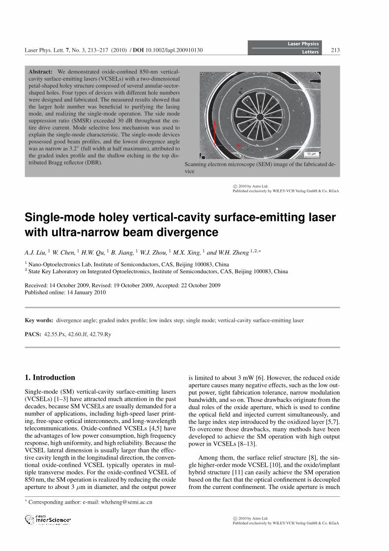
Abstract: We demonstrated oxide-confined 850-nm vertical-cavity surface-emitting lasers (VCSELs) with a two-dimensionalpetal-shaped holey structure composed of several annular-sector-shaped holes. Four types of devices with different hole numberswere designed and fabricated. The measured results showed thatthe larger hole number was beneficial to purifying the lasingmode, and realizing the single-mode operation. The side modesuppression ratio (SMSR) exceeded 30 dB throughout the en-tire drive current. Mode selective loss mechanism was used toexplain the single-mode characteristic. The single-mode devicespossessed good beam profiles, and the lowest divergence anglewas as narrow as 3.2◦ (full width at half maximum), attributed tothe graded index profile and the shallow etching in the top dis-tributed Bragg reflector (DBR).
10 μm
x
y
Scanning electron microscope (SEM) image of the fabricated de-vice
c© 2010 by Astro Ltd.Published exclusively by WILEY-VCH Verlag GmbH & Co. KGaA
Single-mode holey vertical-cavity surface-emitting laserwith ultra-narrow beam divergence
A.J. Liu, 1 W. Chen, 1 H.W. Qu, 1 B. Jiang, 1 W.J. Zhou, 1 M.X. Xing, 1 and W.H. Zheng 1,2,∗
1 Nano-Optoelectronics Lab, Institute of Semiconductors, CAS, Beijing 100083, China2 State Key Laboratory on Integrated Optoelectronics, Institute of Semiconductors, CAS, Beijing 100083, China
Received: 14 October 2009, Revised: 19 October 2009, Accepted: 22 October 2009Published online: 14 January 2010
Key words: divergence angle; graded index profile; low index step; single mode; vertical-cavity surface-emitting laser
PACS: 42.55.Px, 42.60.Jf, 42.79.Ry
1. Introduction
Single-mode (SM) vertical-cavity surface-emitting lasers(VCSELs) [1–3] have attracted much attention in the pastdecades, because SM VCSELs are usually demanded for anumber of applications, including high-speed laser print-ing, free-space optical interconnects, and long-wavelengthtelecommunications. Oxide-confined VCSELs [4,5] havethe advantages of low power consumption, high frequencyresponse, high uniformity, and high reliability. Because theVCSEL lateral dimension is usually larger than the effec-tive cavity length in the longitudinal direction, the conven-tional oxide-confined VCSEL typically operates in mul-tiple transverse modes. For the oxide-confined VCSEL of850 nm, the SM operation is realized by reducing the oxideaperture to about 3 μm in diameter, and the output power
is limited to about 3 mW [6]. However, the reduced oxideaperture causes many negative effects, such as the low out-put power, tight fabrication tolerance, narrow modulationbandwidth, and so on. Those drawbacks originate from thedual roles of the oxide aperture, which is used to confinethe optical field and injected current simultaneously, andthe large index step introduced by the oxidized layer [5,7].To overcome those drawbacks, many methods have beendeveloped to achieve the SM operation with high outputpower in VCSELs [8–13].
Among them, the surface relief structure [8], the sin-gle higher-order mode VCSEL [10], and the oxide/implanthybrid structure [11] can easily achieve the SM operationbased on the fact that the optical confinement is decoupledfrom the current confinement. The oxide aperture is much
∗ Corresponding author: e-mail: [email protected]
c© 2010 by Astro Ltd.Published exclusively by WILEY-VCH Verlag GmbH & Co. KGaA
214 A.J. Liu, W. Chen, et al. : Single-mode holey vertical-cavity surface-emitting laser
RL
0r
r
θ
-contactn
-substraten
-DBRn
Active layersOxide aperture
-DBRp
Holes Opticalaperture
-contactp
effn
(a)
(b)
(c)
10 μm
x
y
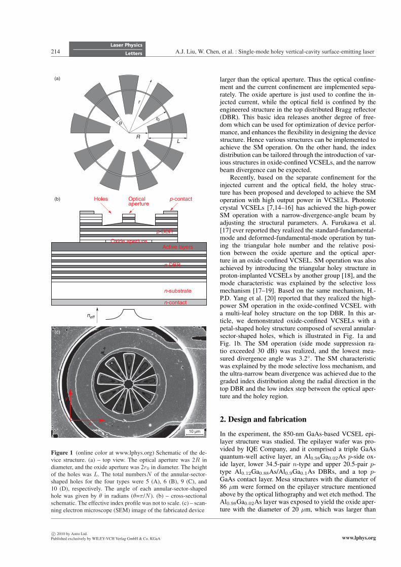
Figure 1 (online color at www.lphys.org) Schematic of the de-vice structure. (a) – top view. The optical aperture was 2R indiameter, and the oxide aperture was 2r0 in diameter. The heightof the holes was L. The total numbersN of the annular-sector-shaped holes for the four types were 5 (A), 6 (B), 9 (C), and10 (D), respectively. The angle of each annular-sector-shapedhole was given by θ in radians (θ=π/N ). (b) – cross-sectionalschematic. The effective index profile was not to scale. (c) – scan-ning electron microscope (SEM) image of the fabricated device
larger than the optical aperture. Thus the optical confine-ment and the current confinement are implemented sepa-rately. The oxide aperture is just used to confine the in-jected current, while the optical field is confined by theengineered structure in the top distributed Bragg reflector(DBR). This basic idea releases another degree of free-dom which can be used for optimization of device perfor-mance, and enhances the flexibility in designing the devicestructure. Hence various structures can be implemented toachieve the SM operation. On the other hand, the indexdistribution can be tailored through the introduction of var-ious structures in oxide-confined VCSELs, and the narrowbeam divergence can be expected.
Recently, based on the separate confinement for theinjected current and the optical field, the holey struc-ture has been proposed and developed to achieve the SMoperation with high output power in VCSELs. Photoniccrystal VCSELs [7,14–16] has achieved the high-powerSM operation with a narrow-divergence-angle beam byadjusting the structural parameters. A. Furukawa et al.[17] ever reported they realized the standard-fundamental-mode and deformed-fundamental-mode operation by tun-ing the triangular hole number and the relative posi-tion between the oxide aperture and the optical aper-ture in an oxide-confined VCSEL. SM operation was alsoachieved by introducing the triangular holey structure inproton-implanted VCSELs by another group [18], and themode characteristic was explained by the selective lossmechanism [17–19]. Based on the same mechanism, H.-P.D. Yang et al. [20] reported that they realized the high-power SM operation in the oxide-confined VCSEL witha multi-leaf holey structure on the top DBR. In this ar-ticle, we demonstrated oxide-confined VCSELs with apetal-shaped holey structure composed of several annular-sector-shaped holes, which is illustrated in Fig. 1a andFig. 1b. The SM operation (side mode suppression ra-tio exceeded 30 dB) was realized, and the lowest mea-sured divergence angle was 3.2◦. The SM characteristicwas explained by the mode selective loss mechanism, andthe ultra-narrow beam divergence was achieved due to thegraded index distribution along the radial direction in thetop DBR and the low index step between the optical aper-ture and the holey region.
2. Design and fabrication
In the experiment, the 850-nm GaAs-based VCSEL epi-layer structure was studied. The epilayer wafer was pro-vided by IQE Company, and it comprised a triple GaAsquantum-well active layer, an Al0.98Ga0.02As p-side ox-ide layer, lower 34.5-pair n-type and upper 20.5-pair p-type Al0.12Ga0.88As/Al0.9Ga0.1As DBRs, and a top p-GaAs contact layer. Mesa structures with the diameter of86 μm were formed on the epilayer structure mentionedabove by the optical lithography and wet etch method. TheAl0.98Ga0.02As layer was exposed to yield the oxide aper-ture with the diameter of 20 μm, which was larger than
c© 2010 by Astro Ltd.Published exclusively by WILEY-VCH Verlag GmbH & Co. KGaA www.lphys.org
Laser Phys. Lett. 7, No. 3 (2010) 215
Ligh
t, m
W
4
3
2
1
0
5
6
7
8
4035302520151050
Current, mA
type A, 5 holestype B, 6 holestype C, 9 holestype D, 10 holes
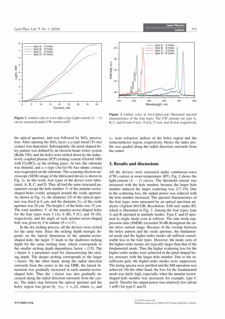
Figure 2 (online color at www.lphys.org) Light-current (L − I)curves measured under CW current at RT
the optical aperture, and was followed by SiO2 passiva-tion. After opening the SiO2 layer, a p-type metal (Ti-Au)contact was deposited. Subsequently, the petal-shaped ho-ley pattern was defined by an electron beam writer system(Raith 150), and the holes were etched down by the induc-tively coupled plasma (ICP) etching system (Oxford 100)with Cl2/BCl3 as the etching gases. At last, the substratewas thinned, and a n-type (Au-Ge-Ni-Au) ohmic contactwas evaporated on the substrate. The scanning electron mi-croscope (SEM) image of the fabricated device is shown inFig. 1c. In this work, four types of the device were fabri-cated, A, B, C, and D. They all had the same structural pa-rameters except the hole number N of the annular-sector-shaped holes evenly arranged around the oxide aperture.As shown in Fig. 1a, the diameter 2R of the optical aper-ture was fixed at 6 μm, and the diameter 2r0 of the oxideaperture was 20 μm. The height L of the holes was 15 μm.The total numbers N of the annular-sector-shaped holesfor the four types were 5 (A), 6 (B), 9 (C), and 10 (D),respectively, and the angle of each annular-sector-shapedhole was given by θ in radians (θ = π/N ).
In the dry etching process, all the devices were etchedfor the same time. Since the etching depth strongly de-pends on the lateral dimension of the annular-sector-shaped hole, the larger N leads to the shallower etchingdepth for the same etching time, which corresponds tothe smaller etching depth dependence factor γ [15]. Theγ-factor is a parameter used for characterizing the etch-ing depth. The deeper etching corresponds to the largerγ-factor. On the other hand, along the radial directionoutwards from the center in the top DBR, the lateral di-mension was gradually increased in each annular-sector-shaped hole. Thus the γ-factor was also gradually in-creased along the radial direction outwards from the cen-ter. The index step between the optical aperture and theholey region was given by γ(na + ns)/2, where na and
Inte
nsity
, a.u
.
-40
-30
-20
-50
-60
848843 844 845 846 847
Wavelength, nm
type A, 5 holestype B, 6 holestype C, 9 holestype D, 10 holes
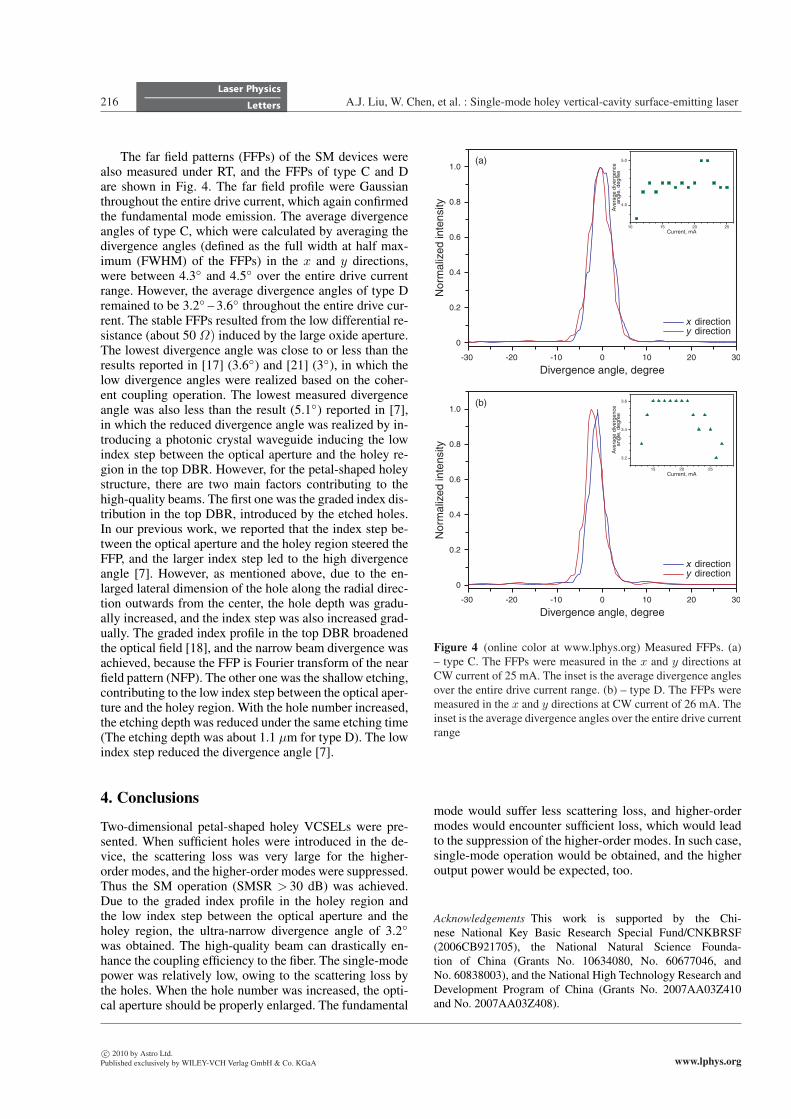
Figure 3 (online color at www.lphys.org) Measured spectralcharacteristics of the four types. The CW currents for type A,B, C, and D were 9 mA, 15 mA, 27 mA, and 26 mA, respectively
ns were refractive indices of the holey region and thesemiconductor region, respectively. Hence the index pro-file was graded along the radial direction outwards fromthe center.
3. Results and discussions
All the devices were measured under continuous-wave(CW) current at room temperature (RT). Fig. 2 shows thelight-current (L − I) curves. The threshold current wasincreased with the hole number, because the larger holenumber induced the larger scattering loss [17–19]. Dueto the scattering loss, the output power was reduced withthe hole number increased. The spectral characteristics ofthe four types were measured by an optical spectrum an-alyzer (Agilent 86142B, Resolution: 0.06 nm) under RT,which is illustrated in Fig. 3. Among the four types, typeA and B operated in multiple modes. Type C and D oper-ated in single mode even at rollover. The side mode sup-pression ratio (SMSR) exceeded 30 dB throughout the en-tire drive current range. Because of the overlap betweenthe holey pattern and the oxide aperture, the fundamen-tal mode and the higher-order modes all suffered consid-erable loss in the four types. However, the mode sizes ofthe higher-order modes are typically larger than that of thefundamental mode. Thus the higher scattering loss for thehigher-order modes were achieved in the petal-shaped ho-ley structure with the larger hole number. Due to the in-sufficient gain, the higher-order modes were suppressed.The lasing spectra were purified and the SM operation wasachieved. On the other hand, the loss for the fundamentalmode was fairly high, especially when the annular-sector-shaped hole number was increased, for example, type Cand D. Thereby the output power was relatively low (about1 mW) for type C and D.
www.lphys.orgc© 2010 by Astro Ltd.
Published exclusively by WILEY-VCH Verlag GmbH & Co. KGaA
216 A.J. Liu, W. Chen, et al. : Single-mode holey vertical-cavity surface-emitting laser
The far field patterns (FFPs) of the SM devices werealso measured under RT, and the FFPs of type C and Dare shown in Fig. 4. The far field profile were Gaussianthroughout the entire drive current, which again confirmedthe fundamental mode emission. The average divergenceangles of type C, which were calculated by averaging thedivergence angles (defined as the full width at half max-imum (FWHM) of the FFPs) in the x and y directions,were between 4.3◦ and 4.5◦ over the entire drive currentrange. However, the average divergence angles of type Dremained to be 3.2◦ – 3.6◦ throughout the entire drive cur-rent. The stable FFPs resulted from the low differential re-sistance (about 50 Ω) induced by the large oxide aperture.The lowest divergence angle was close to or less than theresults reported in [17] (3.6◦) and [21] (3◦), in which thelow divergence angles were realized based on the coher-ent coupling operation. The lowest measured divergenceangle was also less than the result (5.1◦) reported in [7],in which the reduced divergence angle was realized by in-troducing a photonic crystal waveguide inducing the lowindex step between the optical aperture and the holey re-gion in the top DBR. However, for the petal-shaped holeystructure, there are two main factors contributing to thehigh-quality beams. The first one was the graded index dis-tribution in the top DBR, introduced by the etched holes.In our previous work, we reported that the index step be-tween the optical aperture and the holey region steered theFFP, and the larger index step led to the high divergenceangle [7]. However, as mentioned above, due to the en-larged lateral dimension of the hole along the radial direc-tion outwards from the center, the hole depth was gradu-ally increased, and the index step was also increased grad-ually. The graded index profile in the top DBR broadenedthe optical field [18], and the narrow beam divergence wasachieved, because the FFP is Fourier transform of the nearfield pattern (NFP). The other one was the shallow etching,contributing to the low index step between the optical aper-ture and the holey region. With the hole number increased,the etching depth was reduced under the same etching time(The etching depth was about 1.1 μm for type D). The lowindex step reduced the divergence angle [7].
4. Conclusions
Two-dimensional petal-shaped holey VCSELs were pre-sented. When sufficient holes were introduced in the de-vice, the scattering loss was very large for the higher-order modes, and the higher-order modes were suppressed.Thus the SM operation (SMSR > 30 dB) was achieved.Due to the graded index profile in the holey region andthe low index step between the optical aperture and theholey region, the ultra-narrow divergence angle of 3.2◦was obtained. The high-quality beam can drastically en-hance the coupling efficiency to the fiber. The single-modepower was relatively low, owing to the scattering loss bythe holes. When the hole number was increased, the opti-cal aperture should be properly enlarged. The fundamental
Nor
mal
ized
inte
nsity
0
0.2
0.4
0.6
0.8
1.0
3020100-10-20-30
Divergence angle, degree
directionxdirectiony
Ave
rage
div
erge
nce
angl
e, d
egre
e
5.0
4.0
Current, mA10 15 20 25
(a)
Nor
mal
ized
inte
nsity
0
0.2
0.4
0.6
0.8
1.0
3020100-10-20-30
Divergence angle, degree
directionxdirectiony
Ave
rage
div
erge
nce
angl
e, d
egre
e
3.6
3.4
3.2
Current, mA15 20 25
(b)
Figure 4 (online color at www.lphys.org) Measured FFPs. (a)– type C. The FFPs were measured in the x and y directions atCW current of 25 mA. The inset is the average divergence anglesover the entire drive current range. (b) – type D. The FFPs weremeasured in the x and y directions at CW current of 26 mA. Theinset is the average divergence angles over the entire drive currentrange
mode would suffer less scattering loss, and higher-ordermodes would encounter sufficient loss, which would leadto the suppression of the higher-order modes. In such case,single-mode operation would be obtained, and the higheroutput power would be expected, too.
Acknowledgements This work is supported by the Chi-nese National Key Basic Research Special Fund/CNKBRSF(2006CB921705), the National Natural Science Founda-tion of China (Grants No. 10634080, No. 60677046, andNo. 60838003), and the National High Technology Research andDevelopment Program of China (Grants No. 2007AA03Z410and No. 2007AA03Z408).
c© 2010 by Astro Ltd.Published exclusively by WILEY-VCH Verlag GmbH & Co. KGaA www.lphys.org
Laser Phys. Lett. 7, No. 3 (2010) 217
References
[1] K. Iga, F. Koyama, and S. Kinoshita, IEEE J. Quantum Elec-tron. 24, 1845 (1988).
[2] V.M.N. Passaro, F. Magno, and F. De Leonardis, Laser Phys.Lett. 2, 239 (2005).
[3] F. Principato, G. Ferrante, and F. Marin, Laser Phys. Lett. 4,204 (2007).
[4] J.M. Dallesasse, N. Holonyak, Jr., A.R. Sugg, T.A. Richard,and N. El-Zein, Appl. Phys. Lett. 57, 2844 (1990).
[5] K.L. Lear, K.D. Choquette, R.P. Schneider, Jr., and S.P. Kil-coyne, Appl. Phys. Lett. 66, 2616 (1995).
[6] B. Weigl, M. Grabherr, R. Michalzik, G. Reiner, and K.J.Ebeling, IEEE Photonics Technol. Lett. 8, 971 (1996).
[7] A.J. Liu, M.X. Xing, H.W. Qu, W. Chen, W.J. Zhou, andW.H. Zheng, Appl. Phys. Lett. 94, 191105 (2009).
[8] A. Haglund, J.S. Gustavsson, J. Vukusic, P. Modh, and A.Larsson, IEEE Photonics Technol. Lett. 16, 368 (2004).
[9] D. Zhou and L.J. Mawst, IEEE J. Quantum Electron. 38,1599 (2002).
[10] S. Shinada and F. Koyama, IEEE Photonics Technol. Lett.14, 1641 (2002).
[11] E.W. Young, K.D. Choquette, S.L. Chuang, K.M. Geib, A.J.Fischer, and A.A. Allerman, IEEE Photonics Technol. Lett.13, 927 (2001).
[12] M.C.Y. Huang, Y. Zhou, and C.J. Chang-Hasnain, NaturePhoton. 1, 119 (2007).
[13] J.M. Ostermann, F. Rinaldi, P. Debernardi, and R.Michalzik, IEEE Photonics Technol. Lett. 17, 2256 (2005).
[14] D.-S. Song, S.-H. Kim, H.-G. Park, C.-K. Kim, and Y.-H.Lee, Appl. Phys. Lett. 80, 3901 (2002).
[15] N. Yokouchi, A.J. Danner, and K.D. Choquette, Appl. Phys.Lett. 82, 1344 (2003).
[16] T. Czyszanowski, M. Dems, and K. Panajotov, J. Phys. D40, 2732 (2007).
[17] A. Furukawa, S. Sasaki, M. Hoshi, A. Matsuzono, K. Mori-toh, and T. Baba, Appl. Phys. Lett. 85, 5161 (2004).
[18] P.O. Leisher, A.J. Danner, J.J. Raftery, D. Siriani, and K.D.Choquette, IEEE J. Quantum Electron. 42, 1091 (2006).
[19] K. Morito, D. Mori, E. Mizuta, and T. Baba, Proc. of SPIE5722, 191 (2005).
[20] H.-P.D. Yang, I.-C. Hsu, F.-I. Lai, H.-C. Kuo, and J.Y. Chi,Jpn. J. Appl. Phys. 45, L871 (2006).
[21] J. Lin, J.K. Gamelin, G.T. Du, S. Wang, M. Hong, and J.P.Mannaerts, Appl. Phys. Lett. 60, 2851 (1992).
www.lphys.orgc© 2010 by Astro Ltd.
Published exclusively by WILEY-VCH Verlag GmbH & Co. KGaA