Silicon-based Ultra Compact Cost-efficient System Design ... · 6 1.2. Terminology and Symbol...
52
Silicon-based Ultra Compact Cost-efficient System Design for mmWave Sensors “SUCCESS” Deliverable D4.2 Processor FPGA test report (Confidential, results not published) By: EVA and IHP Contributors: Marcin Zys, Piotr Penkala and Mariusz Twardoch (EVA) Miroslav Marinkovic and Yaoming Sun (IHP) Abstract Synchronous signal processor has been verified in an FPGA boards. All functionalities have been tested. The digital control of AFE has also be designed and tested. Keywords Digital processor, FMCW/CW signal generation, FPGA verification
Transcript of Silicon-based Ultra Compact Cost-efficient System Design ... · 6 1.2. Terminology and Symbol...
Silicon-based Ultra Compact Cost-efficient System Design for mmWave
Sensors “SUCCESS”
Deliverable
D4.2
Processor FPGA test report
(Confidential, results not published)
By: EVA and IHP
Contributors:
Marcin Zys, Piotr Penkala and Mariusz Twardoch (EVA)
Miroslav Marinkovic and Yaoming Sun (IHP)
Abstract
Synchronous signal processor has been verified in an FPGA boards. All functionalities
have been tested. The digital control of AFE has also be designed and tested.
Keywords
Digital processor, FMCW/CW signal generation, FPGA verification
2
Table of Contents
1.1. Overview ______________________________________________________ 5 1.2. Terminology and Symbol Conventions ________________________________ 6 1.3. References _____________________________________________________ 6 3.1. Installation _____________________________________________________ 8 3.2. PC Application User Guide _________________________________________ 8 3.3. Typical Usage of the Application____________________________________ 12 3.4. Scripts Usage __________________________________________________ 13 4.1. Access to AFE __________________________________________________ 18 4.2. Access to PLL __________________________________________________ 18 6.1. CW radar mode ________________________________________________ 20 6.2. FMCW radar mode ______________________________________________ 22 6.3. AFE interface __________________________________________________ 27 6.4. PLL interface___________________________________________________ 29 6.5. Auxiliary DAC interface___________________________________________ 30 6.6. Auxiliary ADC interface___________________________________________ 31 6.7. Access to XRAM ________________________________________________ 32 6.8. Access to CW coprocessor registers _________________________________ 33 6.9. Access to FMCW coprocessor registers_______________________________ 34 6.10. One shot CW radar mode _______________________________________ 35 6.11. One shot FMCW radar mode_____________________________________ 38 6.12. CW radar mode with not default configuration_______________________ 43 6.13. FMCW radar mode with not default configuration ____________________ 44 7.1. Digital Control Block Diagram _____________________________________ 46 7.2. Digital Control Pin Description _____________________________________ 47 7.3. SPI Register Map _______________________________________________ 48 7.4. 1.4 Digital Control Functionality____________________________________ 49 7.5. Test results of the first chip version_________________________________ 51
3
List of Figures
Figure 1. Block diagram of the Baseband Processor system prototyped in the FPGA .......................... 7
Figure 2. User tab ......................................................................................................................... 8
Figure 3. SFR Operation................................................................................................................. 9
Figure 4. Models panel................................................................................................................... 9
Figure 5. Radar panel ...................................................................................................................10
Figure 6. Info panel ......................................................................................................................11
Figure 7. Log panel ......................................................................................................................11
Figure 8. Debug tab......................................................................................................................12
Figure 9. Application algorithm diagram.........................................................................................19
Figure 10. Debug panel view for CW mode, distance 1400 mm .......................................................37
Figure 11. Debug panel view for CW mode, distance 1000 mm .......................................................37
Figure 12. Debug panel view for FMCW mode, distance 1500 mm...................................................42
Figure 13. Debug panel view for FMCW mode, distance 4500 mm...................................................42
Figure 14. Block diagram of digital control block.............................................................................46
Figure 15. SPI data transmission format. .......................................................................................50
Figure 16. Diagram flow of test procedures....................................................................................52

4
List of Tables
Table 1. Abbreviations and acronyms ............................................................................................. 6
Table 2. Register map ..................................................................................................................15
Table 3. Write to AFE register .......................................................................................................18
Table 4. Read to AFE register........................................................................................................18
Table 5. Write to PLL register........................................................................................................18
Table 6. Calculated distances for CW mode....................................................................................22
Table 7. Calculated distances for FMCW mode ...............................................................................26
Table 8. Pin Description of Digital Control ......................................................................................47
Table 9. SPI Register Map.............................................................................................................48
Table 10. Write SPI register ..........................................................................................................50
Table 11. Read to SPI register.......................................................................................................50
Table 12. Programming the frequency ramp for DAC testing ...........................................................51
Table 13. Test results of the first chip version ................................................................................52

5
1. Introduction
1.1. Overview
1.1.1 Purpose of Document
This document presents tests executed to validate FPGA prototype of the Baseband Processor, which was developed within the SUCCESS project.
The document also contains user manual for PC application used for FPGA tests. The
application is referred further in the document as the SUCCESS PC Application. The digital control of the AFE is also developed to interface the AFE and processor. It includes an SPI,
frequency counting control, waveform control, clock synchronous etc..
1.1.2 FPGA tests purpose
Tests executed on FPGA aimed in validation of correctness of Baseband Processor operation.
To allow that the Baseband Processor was implemented in FPGA together with a number of
additional modules used to emulate behavior of the other radar blocks (e.g. Analog Front-End, ADC, DAC, PLL).
1.1.3 SUCCESS PC Application purpose
The SUCCESS PC Application allows communicating with Baseband Processor System. Main
features of the application are as follows:
• read and write coprocessors any of the control register implemented in the Baseband
Processor system
• control the operation of the Baseband Processor
• read the calculated distance
• transfer to the FIFO implemented in the FPGA data samples generated in MATLAB
• visualize data samples and FFT calculation result
1.1.4 AFE digital control test
• To validate the mixed signal operation of AFE and digital control
• To verify the possibility of programming output waveform of the transmitter from a PC
6
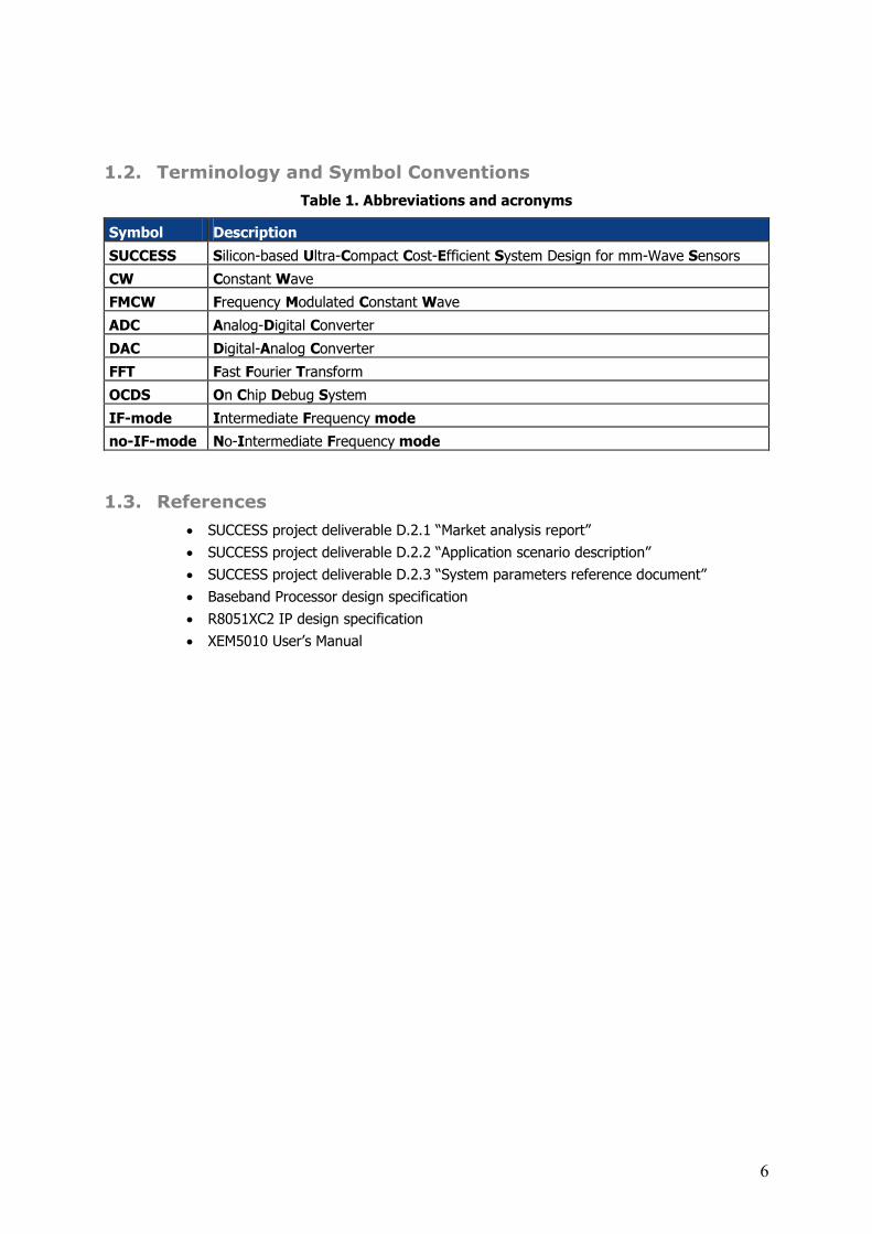
1.2. Terminology and Symbol Conventions
Table 1. Abbreviations and acronyms
Symbol Description
SUCCESS Silicon-based Ultra-Compact Cost-Efficient System Design for mm-Wave Sensors
CW Constant Wave
FMCW Frequency Modulated Constant Wave
ADC Analog-Digital Converter
DAC Digital-Analog Converter
FFT Fast Fourier Transform
OCDS On Chip Debug System
IF-mode Intermediate Frequency mode
no-IF-mode No-Intermediate Frequency mode
1.3. References
• SUCCESS project deliverable D.2.1 “Market analysis report”
• SUCCESS project deliverable D.2.2 “Application scenario description”
• SUCCESS project deliverable D.2.3 “System parameters reference document”
• Baseband Processor design specification
• R8051XC2 IP design specification
• XEM5010 User’s Manual

7
2. Baseband Processor
Detailed description of the Baseband Processor can be found in the Baseband Processor
design specification.
The diagram below presents block diagram of the system prototyped in the FPGA. The system
integrated, besides the baseband Processor, additional modules emulating other radar blocks, like Analog Front-End, ADC, DAC or PLL.
Figure 1. Block diagram of the Baseband Processor system prototyped in the FPGA

8
3. PC Application
3.1. Installation
The PC application is provided as single EXE file, so installation is straightforward – simple copy main executable into desired place. For running application it is necessary to
install a Opal Kelly XEM5010 board drivers and copy libFrontPanel-pinv.dll file to the application directory.
3.2. PC Application User Guide
The PC application consists of two panels:
• User – for configuration and using a hardware system
• Debug – for reading samples and FFT for debugging
3.2.1 User panel description
Figure 2. User tab
User panel is divided into several parts:
a) Hardware connection
In the lower right corner are three buttons for connection to hardware FPGA board.
Initialize device – using for board detection and connection.

9
FPGA Conf – using for FPGA programming from fpga_chip.bit, which is located in the application directory.
FPGA Conf … - using for FPGA programming from user defined file.
b) SFR Operation panel
Figure 3. SFR Operation
This panel is for accessing registers of the Baseband Processor system. It allows to read or write any of the register from the register map. Selection of register is possible by
selection the device and the device register from the combo box or through the register address entry.
c) Models panel
Figure 4. Models panel
In the FPGA are implemented a few models of external devices, it’s possible to use either
these models or external devices. After selection of required configuration Reconnect button must be pressed.

10
d) Radar panel
Figure 5. Radar panel
In this panel the following actions can be done:
• start the Baseband Processor with the required operation mode
• stop the Baseband Processor
• read a distance calculated by the Baseband Processor
• set a size of FFT window for FMCW mode and configure FFT window
• transfer to the FPGA FIFO data samples generated in MATLAB

11
e) Info panel
Figure 6. Info panel
This panel inform about:
• error in FPGA FIFO
• PLL lock state
• CW/FMCW mode
f) Log panel
Figure 7. Log panel
In log window there is written all messages informing about the Baseband Processor
operation, like register accesses, interrupts and script commands.
The application automatically services interrupt from a PLL model and AFE model. In
normal view notification related with PLL and AFE interrupt are not logged. After selecting Detailed View check box, all notifications, including PLL and AFE models interrupts , are
logged.
Run Script … - this button is used to launch a scripts file containing test/operation
scenario.

12
Abort Script – breaking the script operation.
Save Log – save information from the log window to text file.
Clear Log – clear the low window.
3.2.2 Debug tab
Figure 8. Debug tab
Debug tab is used to debug the Baseband Processor operation. In this tab samples from
FPGA FIFO can be read back and displayed at the chart. Moreover, calculated raw FFT result can be read from the FMCW coprocessor and displayed at the FFT spectrum.
3.3. Typical Usage of the Application
3.3.1 FMCW mode
• PLL lock state
• Click Initialize button for board connection
• Click FPGA Conf button to program the FPGA
• Transfer a MATLAB data samples to FPGA (ADC Data: FMCW button)
• Set a FFT window size (FFT Window - size)
• Configure FFT window (FFT Window)
• Configure Baseband Processor mode (set FMCW mode)
• Start the Baseband Processor (Start Radar).
13
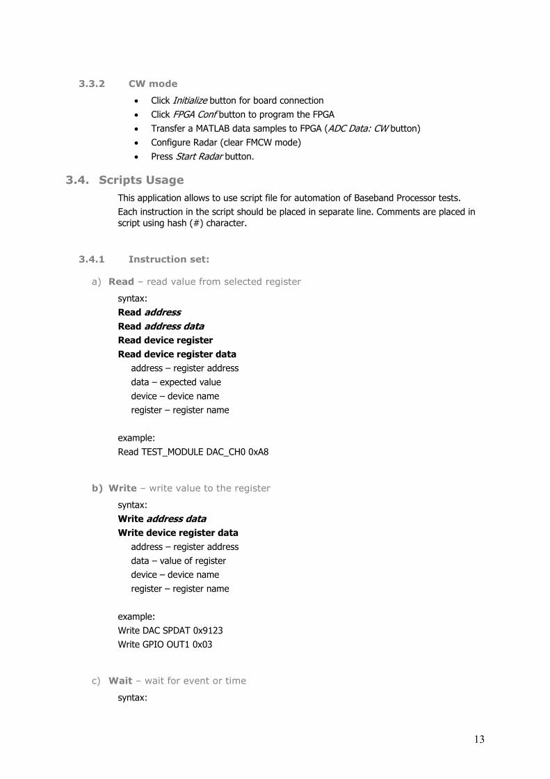
3.3.2 CW mode
• Click Initialize button for board connection
• Click FPGA Conf button to program the FPGA
• Transfer a MATLAB data samples to FPGA (ADC Data: CW button)
• Configure Radar (clear FMCW mode)
• Press Start Radar button.
3.4. Scripts Usage
This application allows to use script file for automation of Baseband Processor tests.
Each instruction in the script should be placed in separate line. Comments are placed in
script using hash (#) character.
3.4.1 Instruction set:
a) Read – read value from selected register
syntax:
Read address
Read address data
Read device register
Read device register data
address – register address
data – expected value
device – device name
register – register name
example:
Read TEST_MODULE DAC_CH0 0xA8
b) Write – write value to the register
syntax:
Write address data
Write device register data
address – register address
data – value of register
device – device name
register – register name
example:
Write DAC SPDAT 0x9123
Write GPIO OUT1 0x03
c) Wait – wait for event or time
syntax:
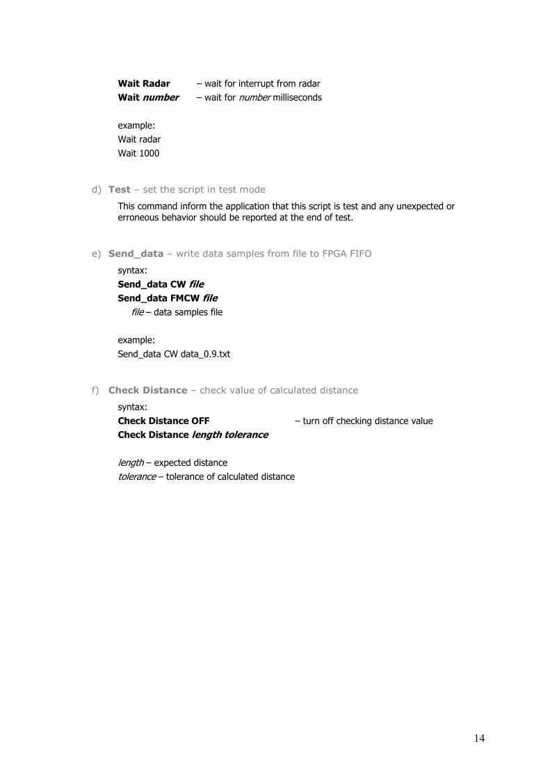
14
Wait Radar – wait for interrupt from radar
Wait number – wait for number milliseconds
example:
Wait radar
Wait 1000
d) Test – set the script in test mode
This command inform the application that this script is test and any unexpected or
erroneous behavior should be reported at the end of test.
e) Send_data – write data samples from file to FPGA FIFO
syntax:
Send_data CW file
Send_data FMCW file
file – data samples file
example:
Send_data CW data_0.9.txt
f) Check Distance – check value of calculated distance
syntax:
Check Distance OFF – turn off checking distance value
Check Distance length tolerance
length – expected distance
tolerance – tolerance of calculated distance

15
4. FPGA System Register Map
The table below presents a memory map of the FPGA Baseband Processor system that can be
accessed by the PC application.
Table 2. Register map
Register Locati
on
Reset
value
Access Description
Baseband Processor - AFE interface
SPSTA 0x0001 0x00 R/W SPI Status Register
SPCON 0x0002 0x00 R/W SPI Control Register
SPDAT 0x0003 0x00 R/W SPI Data Register
SPSSN 0x0008 0x00 R/W SPI Slave Select Register
Baseband Processor - CW PROC
DELTA_FR_LOW 0x0020 0x00 R/W
DELTA_FR_HIGH 0x0021 0x00 R/W
Frequency difference between 1st and 2nd
measurement
DISCARD_NUM_LOW 0x0022 0x00 R/W
DISCARD_NUM_HIGH
0x0023 0x00 R/W
Number of ADC samples that are to be
discarded after change of measurement
frequency
ANGLE_1_LOW 0x0024 0x00 R
ANGLE_1_MID 0x0025 0x00 R
ANGLE_1_HIGH 0x0026 0x00 R
Sum of angles calculated in measurements
done for 1st frequency
ANGLE_2_LOW 0x0027 0x00 R
ANGLE_2_MID 0x0028 0x00 R
ANGLE_2_HIGH 0x0029 0x00 R
Sum of angles calculated in measurements
done for 2nd frequency
DISTANCE_LOW 0x002A 0x00 R
DISTANCE_MID 0x002B 0x00 R
DISTANCE_HIGH 0x002C 0x00 R
Calculated distance
I_LOW 0x002D 0x00 R
I_HIGH 0x002E 0x00 R
Calculated I part of input signal
Q_LOW 0x002F 0x00 R
Q_HIGH 0x0030 0x00 R
Calculated Q part of input signal
I_DC_LOW 0x0032 0x00 R/W
I_DC_HIGH 0x0033 0x00 R/W
DC offset used for calibration of I part of input signal
I_AMP_LOW 0x0034 0x00 R/W
I_AMP_HIGH 0x0035 0x00 R/W
Amplitude gain used for calibration of I part of
input signal
Q_DC_LOW 0x0036 0x00 R/W
Q_DC_HIGH 0x0037 0x00 R/W
DC offset used for calibration of Q part of
input signal
Q_AMP_LOW 0x0038 0x00 R/W
Q_AMP_HIGH 0x0039 0x00 R/W
Amplitude gain used for calibration of Q part of input signal
AVER_NUM 0x003E 0x00 R/W Averaging number
CW_CTRL 0x003F 0x00 R/W Control register
Baseband Processor - FMCW PROC
SFREQ_LOW 0x0040 0x00 R/W
SFREQ_HIGH 0x0042 0x00 R/W
Sampling frequency
DET_FR0_LOW 0x0042 0x00 R Value of the most significant frequency
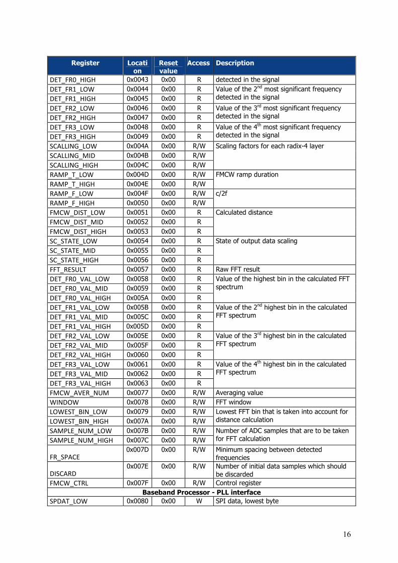
16
Register Location
Reset value
Access Description
DET_FR0_HIGH 0x0043 0x00 R detected in the signal
DET_FR1_LOW 0x0044 0x00 R
DET_FR1_HIGH 0x0045 0x00 R
Value of the 2nd most significant frequency
detected in the signal
DET_FR2_LOW 0x0046 0x00 R
DET_FR2_HIGH 0x0047 0x00 R
Value of the 3rd most significant frequency detected in the signal
DET_FR3_LOW 0x0048 0x00 R
DET_FR3_HIGH 0x0049 0x00 R
Value of the 4th most significant frequency detected in the signal
SCALLING_LOW 0x004A 0x00 R/W
SCALLING_MID 0x004B 0x00 R/W
SCALLING_HIGH 0x004C 0x00 R/W
Scaling factors for each radix-4 layer
RAMP_T_LOW 0x004D 0x00 R/W
RAMP_T_HIGH 0x004E 0x00 R/W
FMCW ramp duration
RAMP_F_LOW 0x004F 0x00 R/W
RAMP_F_HIGH 0x0050 0x00 R/W
c/2f
FMCW_DIST_LOW 0x0051 0x00 R
FMCW_DIST_MID 0x0052 0x00 R
FMCW_DIST_HIGH 0x0053 0x00 R
Calculated distance
SC_STATE_LOW 0x0054 0x00 R
SC_STATE_MID 0x0055 0x00 R
SC_STATE_HIGH 0x0056 0x00 R
State of output data scaling
FFT_RESULT 0x0057 0x00 R Raw FFT result
DET_FR0_VAL_LOW 0x0058 0x00 R
DET_FR0_VAL_MID 0x0059 0x00 R
DET_FR0_VAL_HIGH 0x005A 0x00 R
Value of the highest bin in the calculated FFT
spectrum
DET_FR1_VAL_LOW 0x005B 0x00 R
DET_FR1_VAL_MID 0x005C 0x00 R
DET_FR1_VAL_HIGH 0x005D 0x00 R
Value of the 2nd highest bin in the calculated FFT spectrum
DET_FR2_VAL_LOW 0x005E 0x00 R
DET_FR2_VAL_MID 0x005F 0x00 R
DET_FR2_VAL_HIGH 0x0060 0x00 R
Value of the 3rd highest bin in the calculated
FFT spectrum
DET_FR3_VAL_LOW 0x0061 0x00 R
DET_FR3_VAL_MID 0x0062 0x00 R
DET_FR3_VAL_HIGH 0x0063 0x00 R
Value of the 4th highest bin in the calculated FFT spectrum
FMCW_AVER_NUM 0x0077 0x00 R/W Averaging value
WINDOW 0x0078 0x00 R/W FFT window
LOWEST_BIN_LOW 0x0079 0x00 R/W
LOWEST_BIN_HIGH 0x007A 0x00 R/W
Lowest FFT bin that is taken into account for
distance calculation
SAMPLE_NUM_LOW 0x007B 0x00 R/W
SAMPLE_NUM_HIGH 0x007C 0x00 R/W
Number of ADC samples that are to be taken for FFT calculation
FR_SPACE 0x007D 0x00 R/W Minimum spacing between detected
frequencies
DISCARD 0x007E 0x00 R/W Number of initial data samples which should
be discarded
FMCW_CTRL 0x007F 0x00 R/W Control register
Baseband Processor - PLL interface
SPDAT_LOW 0x0080 0x00 W SPI data, lowest byte

17
Register Location
Reset value
Access Description
SPDAT_HIGH 0x0081 0x00 W SPI data, highest byte
Baseband Processor - auxiliary ADC interface
SPDAT_0 0x0090 0x00 R ADC channel 0 output
SPDAT_4 0x0094 0x00 R ADC channel 1 output
SPDAT_3 0x0093 0x00 R ADC channel 2 output
SPDAT_5 0x0095 0x00 R ADC channel 3 output
SPDAT_2 0x0092 0x00 R ADC channel 4 output
SPDAT_1 0x0091 0x00 R ADC channel 5 output
SPDAT_6 0x0096 0x00 R ADC channel 6 output
SPDAT_7 0x0097 0x00 R ADC channel 7 output
Baseband Processor - auxiliary DAC interface
SPDAT 0x00A0 0x00 W Data to be written to DAC
Baseband Processor - GPIO
OUT0 0x00B0 0x00 R/W State of gp_out Baseband Processor output
OUT1 0x00B1 0x00 R/W Connected to port O of R8051XC2, used to
start Baseband Processor operation from
OUT2 0x00B2 0x00 R/W Unused
OUT3 0x00B3 0x00 R/W Unused
IN0 0x00B4 0x00 R State of gp_in Baseband Processor input
IN1
0x00B5 0x00 R Three least significant bits reflect state of:
IN1[0]: PLL lock IN1[1]: PLL not ready for SPI transfer
IN1[2]: DAC not ready for SPI transfer
IN3 0x00B7 0x00 R Unused, fixed to 0
IN2 0x00B6 0x00 R Unused, fixed to 0
R0 0x00B8 0x00 R/W
R1
0x00B9 0x00 R/W
Distance calculated by the Baseband
Processor is written o this register, so that it could be read by the HOST (PC application)
through USB
R2 0x00BA 0x00 R/W Unused
R3 0x00BB 0x00 R/W Unused
Baseband Processor - RAM
XRAM
0x0200 …
0x03FF
0x00 R/W R8051XC2 external RAM
TEST MODULEs – outside the Baseband Processor
RAMP 0x1000 0x00 W Configuration of RAMP period used to
generate ramp output
AFE
0x1001 0x00 R/W Used to read value received by AFE model
through SPI, or write value that is to be sent back by AFE model through SPI
PLL_HIGH 0x1003 0x00 R
PLL_LOW 0x1002 0x00 R
Used to read value received by PLL model
through SPI
ADC_CH0 0x1010 0x00 W
ADC_CH1 0x1011 0x00 W
ADC_CH2 0x1012 0x00 W
ADC_CH3 0x1013 0x00 W
ADC_CH4 0x1014 0x00 W
ADC_CH5 0x1015 0x00 W
Used to set value of ADC channel
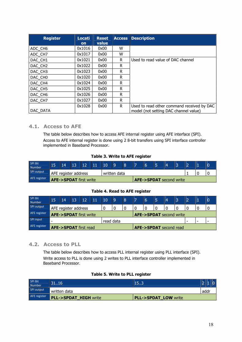
18
Register Location
Reset value
Access Description
ADC_CH6 0x1016 0x00 W
ADC_CH7 0x1017 0x00 W
DAC_CH1 0x1021 0x00 R
DAC_CH2 0x1022 0x00 R
DAC_CH3 0x1023 0x00 R
DAC_CH0 0x1020 0x00 R
DAC_CH4 0x1024 0x00 R
DAC_CH5 0x1025 0x00 R
DAC_CH6 0x1026 0x00 R
DAC_CH7 0x1027 0x00 R
Used to read value of DAC channel
DAC_DATA 0x1028 0x00 R Used to read other command received by DAC
model (not setting DAC channel value)
4.1. Access to AFE
The table below describes how to access AFE internal register using AFE interface (SPI).
Access to AFE internal register is done using 2 8-bit transfers using SPI interface controller
implemented in Baseband Processor.
Table 3. Write to AFE register
SPI Bit
Number 15 14 13 12 11 10 9 8 7 6 5 4 3 2 1 0
SPI output AFE register address written data 1 0 0
AFE register AFE->SPDAT first write AFE->SPDAT second write
Table 4. Read to AFE register
SPI Bit
Number 15 14 13 12 11 10 9 8 7 6 5 4 3 2 1 0
SPI output AFE register address 0 0 0 0 0 0 0 0 0 0 0
AFE register AFE->SPDAT first write AFE->SPDAT second write
SPI input - read data - - -
AFE register AFE->SPDAT first read AFE->SPDAT second read
4.2. Access to PLL
The table below describes how to access PLL internal register using PLL interface (SPI).
Write access to PLL is done using 2 writes to PLL interface controller implemented in Baseband Processor.
Table 5. Write to PLL register
SPI Bit
Number 31..16 15..3 2 1 0
SPI output written data addr
AFE register PLL->SPDAT_HIGH write PLL->SPDAT_LOW write

19
5. PC application algorithm
The diagram below presents a block diagram of the algorithm implemented in the PC
application.
Figure 9. Application algorithm diagram

20
6. FPGA Tests
6.1. CW radar mode
6.1.1 Test description
The test validates the operational of the Baseband Processor in CW mode. The test validates the correctness of calculation of the distance between radar and target object. The calculation
is based on the data generated in MATLAB. The generated data emulate the operation of the analog part of the radar connected to Baseband Processor by ADC interface.
Generation of data in MATLAB is based on CW algorithm a pre-defined value of distance to the
target. This distance calculated in the Baseband Processor must be consistent with value set during generation of MATLAB. Any differences may result from algorithm accuracy and
calculation precision. For each distance, it is defined in the test script, a maximum difference between calculated distance and the actual distance.
6.1.2 Test scenario
The typescript below shows the a part of the test script which contains a validation of the two distance calculations.
1. Write GPIO OUT1 0x0001
2. Send_data CW data_1.4.txt
3. Wait Radar
4. Check Distance 1400 10
5. Wait 500
6. Check Distance OFF
7. Send_data CW data_1.2.txt
8. Wait Radar
9. Check Distance 1200 10
10. Wait 500
11. Check Distance OFF
In the first line write command set the register OUT1 of the GPIO block. The register OUT1 is
used to start Baseband Processor operation and sets CW mode. At lines 2 and 7 data samples generated in MATLAB are sent to Baseband Processor which start calculation process. At lines
3 and 8 wait command causes waiting for Baseband Processor interrupt which declares the
end of the calculation process. At line 4 and 9 check distance command compares calculated value with expected value. The last number in this command is the acceptable calculation
accuracy. If the calculated value has higher error then the defined accuracy, the error message is displayed. At lines 6 and 11 check distance off command causes that the PC
application ends the compare operation before loading data corresponding to next value of
distance to a target.
6.1.3 Test procedure
This typescript below shows the a part of the test log which is displayed on the PC application
log panel.
1. Test
2. Write GPIO OUT1 0x0001
21
3. Send_data CW data_1.4.txt
4. Wait Radar
5. Check Distance 1400 10
6. Wait 500
7. Calculated distance: 1396 mm
8. Calculated distance: 1396 mm
9. Calculated distance: 1396 mm
10. …
11. Calculated distance: 1396 mm
12. Calculated distance: 1396 mm
13. Calculated distance: 1396 mm
14. Check Distance OFF
15. Send_data CW data_1.2.txt
16. Wait Radar
17. Check Distance 1200 10
18. Wait 500
19. Calculated distance: 1199 mm
20. Calculated distance: 1199 mm
21. Calculated distance: 1199 mm
22. …
23. Calculated distance: 1199 mm
24. Calculated distance: 1199 mm
25. Calculated distance: 1199 mm
26. Check Distance OFF
27. Send_data CW data_1.0.txt
28. Wait Radar
29. Check Distance 1000 10
30. Wait 500
31. Calculated distance: 995 mm
32. Calculated distance: 995 mm
33. Calculated distance: 995 mm
34. …
35. Calculated distance: 995 mm
36. Calculated distance: 995 mm
37. Calculated distance: 995 mm
38. Check Distance OFF
39. Write GPIO OUT1 0x0000
40. # End of test detected.
The log file is similar to the test script which was presented beforehand. The main difference
is the calculated distance messages. These messages shows that the Baseband Processor
calculation process is performed during the test and all calculated distances are very close to the expected values and their accuracy is within the acceptance range.
The table below presents the comparison of results calculated by the MATLAB algorithm
implementation and Baseband Processor in CW mode.
It can be noticed that the results have similar accuracy. The highest error of MATLAB results
is about 5 mm (for 1000 mm, which is 0.5%) and the highest error of Baseband Processor

22
results is about 7 mm (for 900 mm, which is less than 0.8%). The mean error of MATLAB results is 2 mm the mean error of Baseband Processor results is 2.7 mm.
Analysis of results proves the correctness of CW algorithm implementation in the Baseband
Processor.
Table 6. Calculated distances for CW mode
Distance to
object
MATLAB algorithm result Baseband Processor result Notes
200 200 199
300 300 300
400 401 400
500 501 500
600 600 597
700 704 703
800 801 801
900 902 907
1000 995 995
1100 1096 1093
1200 1197 1199
1400 1404 1396
All Baseband Processor results
with similar accuracy as MATLAB results.
6.1.4 Test result
CW radar mode test was executed successfully. No errors were found and all calculated distances are within the margin of error and this confirms that the Baseband Processor is
working properly in CW mode.
6.2. FMCW radar mode
6.2.1 Test description
The test validates the operational of the Baseband Processor in FMCW mode. The test
validates the correctness of calculation of the distance between radar and target object. The
calculation is based on the data generated in MATLAB. The generated data emulate the operation of the analog part of the radar connected to Baseband Processor by ADC interface.
Generation of data in MATLAB is based on FMCW algorithm a pre-defined value of distance to the target. This distance calculated in the Baseband Processor must be consistent with value
set during generation of MATLAB. Any differences may result from algorithm accuracy and
calculation precision. For each distance, it is defined in the test script, a maximum difference between calculated distance and the actual distance.
6.2.2 Test scenario
The typescript below shows the a part of the test script which contains a validation of the two distance calculations.
1. Write FMCW_PROC WINDOW 0x0001
2. Write FMCW_PROC WINDOW 0x01f4

23
3. Write FMCW_PROC WINDOW 0x0001
4. Write FMCW_PROC WINDOW 0x021c
5. …
6. Write FMCW_PROC WINDOW 0x0120
7. Write FMCW_PROC WINDOW 0x0001
8. Write FMCW_PROC WINDOW 0x00cc
9. Write FMCW_PROC WINDOW 0x0000
10. Write GPIO OUT1 0x0003
11. Send_data FMCW fmcwdata_1.5.txt
12. Wait Radar
13. Check Distance 1500 50
14. Wait 500
15. Check Distance OFF
16. # next distance
17. Send_data FMCW fmcwdata_1.2.txt
18. Wait Radar
19. Check Distance 1200 30
20. Wait 500
21. Check Distance OFF
In first lines (1 to 9) write command sends the 48 values which are the samples that are used to define the Kaiser window. These samples were calculated by the PC Application and copied
to the test script (this operation can be obtained by entering the number into the field next to
the FFT window button and then pressing it). The window function is necessary for FFT computation executed by Baseband Processor. The FFT computation is the part of FMCW
distance calculation.
At line nr 10 write command sets the register OUT1 of the GPIO block. The register OUT1 is
used to start Baseband Processor operation in FMCW mode. At lines 11 and 17 the data
generated in MATLAB are sent to the Baseband Processor which starts calculation process. At lines 12 and 18 wait command causes waiting for Baseband Processor interrupt which
declares the end of the first calculation process. At lines 13 and 19 check distance command compares calculated values with expected values. The last number in this command is the
acceptable calculation accuracy. If the calculated value has higher error then the defined accuracy, the error message is displayed. At lines 14 and 20 check distance off command
causes that the PC application ends the compare operation before loading data corresponding
to next value of distance to a target.
6.2.3 Test process
This typescript below shows the a part of the test log which is displayed on the PC application
log panel.
1. Write FMCW_PROC WINDOW 0x0001
2. Write FMCW_PROC WINDOW 0x01f4
3. …
4. Write FMCW_PROC WINDOW 0x00cc
5. Write FMCW_PROC WINDOW 0x0000
6. Write GPIO OUT1 0x0003
7. Send_data FMCW fmcwdata_1.5.txt
8. All_Distance_Display
9. Wait Radar

24
10. Wait Radar
11. Check Distance 1500 50
12. Wait 500
13. Calculated distance: 1489 mm
14. Calculated distance: 1489 mm
15. …
16. Calculated distance: 1489 mm
17. Calculated distance: 1489 mm
18. Check Distance OFF
19. Send_data FMCW fmcwdata_1.2.txt
20. Wait Radar
21. Wait Radar
22. Check Distance 1200 30
23. Wait 500
24. Calculated distance: 1222 mm
25. Calculated distance: 1222 mm
26. …
27. Calculated distance: 1222 mm
28. Calculated distance: 1222 mm
29. Check Distance OFF
30. Send_data FMCW fmcwdata_1.1.txt
31. Wait Radar
32. Wait Radar
33. Check Distance 1100 45
34. Wait 500
35. Calculated distance: 1141 mm
36. Calculated distance: 1141 mm
37. …
38. Calculated distance: 1141 mm
39. Calculated distance: 1141 mm
40. Check Distance OFF
41. Send_data FMCW fmcwdata_1.0.txt
42. Wait Radar
43. Wait Radar
44. Check Distance 1000 20
45. Wait 500
46. Calculated distance: 998 mm
47. Calculated distance: 998 mm
48. …
49. Calculated distance: 998 mm
50. Calculated distance: 998 mm
51. Check Distance OFF
52. Calculated distance: 998 mm
53. Send_data FMCW fmcwdata_0.9.txt
54. Wait Radar
55. Calculated distance: 998 mm
56. Wait Radar
57. Check Distance 900 20
58. Wait 500

25
59. Calculated distance: 903 mm
60. Calculated distance: 903 mm
61. …
62. Calculated distance: 903 mm
63. Calculated distance: 903 mm
64. Check Distance OFF
65. Send_data FMCW fmcwdata_0.8.txt
66. Wait Radar
67. Wait Radar
68. Check Distance 800 20
69. Wait 500
70. Calculated distance: 819 mm
71. Calculated distance: 819 mm
72. …
73. Calculated distance: 819 mm
74. Calculated distance: 819 mm
75. Check Distance OFF
76. Send_data FMCW fmcwdata_0.7.txt
77. Wait Radar
78. Wait Radar
79. Check Distance 700 60
80. Wait 500
81. Calculated distance: 669 mm
82. Calculated distance: 669 mm
83. …
84. Calculated distance: 669 mm
85. Calculated distance: 669 mm
86. Check Distance OFF
87. Send_data FMCW fmcwdata_0.6.txt
88. Wait Radar
89. Wait Radar
90. Check Distance 600 45
91. Wait 500
92. Calculated distance: 644 mm
93. Calculated distance: 644 mm
94. …
95. Calculated distance: 644 mm
96. Calculated distance: 644 mm
97. Check Distance OFF
98. Send_data FMCW fmcwdata_0.5.txt
99. Wait Radar
100. Wait Radar
101. Check Distance 500 20
102. Wait 500
103. Calculated distance: 483 mm
104. Calculated distance: 483 mm
105. …
106. Calculated distance: 483 mm
107. Calculated distance: 483 mm
26
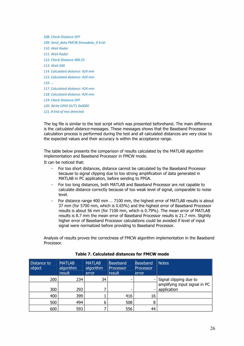
108. Check Distance OFF
109. Send_data FMCW fmcwdata_0.4.txt
110. Wait Radar
111. Wait Radar
112. Check Distance 400 25
113. Wait 500
114. Calculated distance: 424 mm
115. Calculated distance: 424 mm
116. …
117. Calculated distance: 424 mm
118. Calculated distance: 424 mm
119. Check Distance OFF
120. Write GPIO OUT1 0x0000
121. # End of test detected.
The log file is similar to the test script which was presented beforehand. The main difference
is the calculated distance messages. These messages shows that the Baseband Processor calculation process is performed during the test and all calculated distances are very close to
the expected values and their accuracy is within the acceptance range.
The table below presents the comparison of results calculated by the MATLAB algorithm
implementation and Baseband Processor in FMCW mode.
It can be noticed that:
- For too short distances, distance cannot be calculated by the Baseband Processor because to signal clipping due to too strong amplification of data generated in
MATLAB in PC application, before sending to FPGA.
- For too long distances, both MATLAB and Baseband Processor are not capable to calculate distance correctly because of too weak level of signal, comparable to noise
level.
- For distance range 400 mm … 7100 mm, the highest error of MATLAB results is about
37 mm (for 5700 mm, which is 0.65%) and the highest error of Baseband Processor results is about 56 mm (for 7100 mm, which is 0.79%). The mean error of MATLAB
results is 8.7 mm the mean error of Baseband Processor results is 21.7 mm. Slightly
higher error of Baseband Processor calculations could be avoided if level of input signal were normalized before providing to Baseband Processor.
Analysis of results proves the correctness of FMCW algorithm implementation in the Baseband
Processor.
Table 7. Calculated distances for FMCW mode
Distance to object
MATLAB algorithm
result
MATLAB algorithm
error
Baseband Processor
result
Baseband Processor
error
Notes
200 234 34 - -
300 293 7 - -
Signal clipping due to amplifying input signal in PC
application
400 399 1 416 16
500 494 6 508 8
600 593 7 556 44

27
Distance to object
MATLAB algorithm
result
MATLAB algorithm
error
Baseband Processor
result
Baseband Processor
error
Notes
700 696 4 709 9
800 794 6 815 15
900 897 3 925 25
1000 996 4 991 9
1100 1091 9 1083 17
1200 1194 6 1233 33
1500 1490 10 1514 14
2300 2289 11 2312 12
3400 3388 12 3370 30
4500 4498 2 4515 15
5700 5663 37 5778 22
7100 7087 13 7156 56
8500 - - - Level of signal too weak
6.2.4 Test result
FMCW radar mode test was executed successfully. No errors were found and all calculated
distances are within the margin of error and this confirms that the Baseband Processor is
working properly in FMCW mode.
6.3. AFE interface
6.3.1 Test description
The test validates the operation of the Baseband Processor AFE interface and the transmission
protocol between Baseband Processor and AFE.
To allow that verification, simple model of AFE has been implemented and connected to the Baseband Processor AFE interface. PC application has a direct access to AFE model through
the Host interface.
The AFE interface validation was achieved by:
• Forcing from PC application write transaction at the AFE interface (i.e. sending data
from PC application via AFE interface to AFE model) and checking the data received by the AFE model.
• Sending data from PC application to AFE model and forcing from PC application read
transaction at the AFE interface with checking data received at AFE interface.
Additionally, while testing the Baseband Processor in CW and FMCW modes, correctness of AFE interface transactions initiated by the Baseband Processor firmware was tested.
6.3.2 Test scenario
This typescript below shows the a part of the test log which is displayed on the PC application log panel.
1. Write AFE 0x002 0xA1

28
2. Read TEST_MODULE AFE 0x150C
3. Write AFE 0x003 0x02
4. Read TEST_MODULE AFE 0x1814
5. Write AFE 0x004 0x5F
6. Read TEST_MODULE AFE 0x22FC
7. Write AFE 0x005 0xCA
8. Read TEST_MODULE AFE 0x2E54
9. Write AFE 0x006 0x08
10. Read TEST_MODULE AFE 0x3044
11. Write TEST_MODULE AFE 0x008C
12. Read AFE 0x000 0x008C
13. Write TEST_MODULE AFE 0x0944
14. Read AFE 0x001 0x0944
15. Write TEST_MODULE AFE 0x150C
16. Read AFE 0x002 0x150C
17. Write TEST_MODULE AFE 0x1814
18. Read AFE 0x003 0x1814
19. Write TEST_MODULE AFE 0x22FC
20. Read AFE 0x004 0x22FC
The write commands at lines 1, 3, 5, 7, 9 result in sending data to the AFE model via the AFE interface. Sent data corresponds to 8-bit data to be written to selected AFE register. When all
the values are sent, their result is checked by read commands. At lines 2, 4, 6, 8, 10 the read commands result in reading value from AFE model receive buffer. This value is 16-bit length and contains AFE register address, written data and code message. The value is validated by
comparing it with expected value specified together with read command. If a checked value is different than expected, the test fails and error message is displayed.
The write commands at lines 11, 13, 15, 17, 19 result in sending data to the AFE model. Sent data corresponds to 16-bit data to be released at the AFE interface by AFE model during read
transaction. At lines 12, 14, 16, 18, 20 the read commands results in read transaction at the AFE interface which corresponds to reading value from selected register of the AFE model.
This value should be exactly the same as the last value written to the AFE model transmit buffer, what is specified as a parameter of read command. If the read value is different, then
the test fails and error message is displayed.
6.3.3 Baseband Process accessing AFE
To verify communication between the Baseband Processor and AFE model, data which is sent automatically to AFE by the Baseband Processor firmware during CW or FMCW operation is
checked with expected value.
a) CW mode
In the CW mode, to start calculating the Baseband Processor configures the analog part of the radar. It is done by sending the configuration data to AFE model. There
are 4 write access to AFE:
0x9D -> FREQ_H - 0x14EC received by the AFE model
0x56 -> FREQ_L - 0x1AB4 received by the AFE model
0x00 -> CTRL1 - 0x0004 received by the AFE model
0x04-> CTRL2 - 0x0824 received by the AFE model

29
Additionally, while stopping radar, the Baseband Processor makes 1 write access to AFE:
0x01-> CTRL2 - 0x080C received by the AFE model
b) FMCW mode
In the FMCW mode, to start calculating the Baseband Processor configures the analog part of the radar. It is done by sending the configuration data to AFE model. There
are 4 write access to AFE:
0x02 -> CTRL1 - 0x0014 received by the AFE model
0x81-> CTRL2 - 0x0C0C received by the AFE model
0x04-> CTRL2 - 0x0824 received by the AFE model
Additionally, while stopping radar, the Baseband Processor makes 1 write access to
AFE:
0x01-> CTRL2 - 0x080C received by the AFE model
All checked values are as expected. The communication between Baseband Processor and AFE model is working properly.
6.3.4 Test result
AFE interface test was executed successfully. No errors were found and all sending values have been received by AFE model correctly. AFE interface is working properly and provides
trouble-free transport protocol.
6.4. PLL interface
6.4.1 Test description
The test validates the operation of the Baseband Processor PLL interface and the transmission
protocol between Baseband Protocol and PLL.
To allow that verification, simple model of PLL has been implemented and connected to the
Baseband Processor PLL interface. PC application has a direct access to PLL model through the Host interface. The PLL interface validation was achieved by sending data from PC
application via PLL interface to PLL model and checking the data received by the PLL model.
Additionally, while testing the Baseband Processor in CW and FMCW modes, correctness of PLL interface transactions initiated by the Baseband Processor firmware was tested.
6.4.2 Test scenario
The typescript below shows the a part of the test script which contains a validation of PLL interface.
1. Write PLL FRACINT 0x12345678
2. Read TEST_MODULE PLL_LOW 0xb3c0
3. Read TEST_MODULE PLL_HIGH 0x91a2
4. Write PLL PHASE 0x98765432
5. Read TEST_MODULE PLL_LOW 0xA191
6. Read TEST_MODULE PLL_HIGH 0xC3B2
7. Write PLL FUNCTION 0xABCDEF59
8. Read TEST_MODULE PLL_LOW 0x7ACB
9. Read TEST_MODULE PLL_HIGH 0x5E6F

30
The write commands (at lines 1, 4, 6) result is sending 32-bit data to selected register of the
PLL model. Correctness of write transactions at the PLL interface is checked by read commands (at lines 2, 3, 5, 6, 7, 8). The read commands read the value from the PLL module register and compare it with the expected value, specified with the read command. To read
data received by the PLL model, to read access to PLL model are made because the Host is 16- bits and PLL model is 32-bit. If read value is different than expected then test fails and
error message is displayed.
6.4.3 Test result
PLL interface test was executed successfully. No errors were found and all written values have
been received by PLL interface correctly. PLL interface is working properly and provides
trouble-free transport protocol.
6.5. Auxiliary DAC interface
6.5.1 Test description
The test validates the operation of the Auxiliary DAC interface and the transmission protocol
between the Baseband Processor and the Auxiliary DAC.
To allow that verification, simple model of Auxiliary DAC has been implemented and
connected to the Baseband Processor Auxiliary DAC interface. PC application has a direct
access to Auxiliary DAC model through the Host interface. To facilitate verification, the DAC model implements 9 internal registers. 8 of them corresponds to current value of each of 8
channels and 9th reflects of value of last received control word, which is differentiated from channel register access by address > b0111.
The validation was achieved by sending random values from PC application via Baseband
Processor Auxiliary DAC interface to Auxiliary DAC model and validating state of Auxiliary DAC internal registers.
6.5.2 Test scenario
The typescript below shows the a part of the test script which contains a validation of Auxiliary DAC interface.
1. Write DAC SPDAT 0x0000
2. Write DAC SPDAT 0x1000
3. Write DAC SPDAT 0x2000
4. Write DAC SPDAT 0x3000
5. Write DAC SPDAT 0x4000
6. Write DAC SPDAT 0x5000
7. Write DAC SPDAT 0x6000
8. Write DAC SPDAT 0x7000
9. Write DAC SPDAT 0x8000
10. Write DAC SPDAT 0x00A8
11. Read TEST_MODULE DAC_CH0 0xA8
12. Read TEST_MODULE DAC_CH1 0x00
13. Read TEST_MODULE DAC_CH2 0x00
14. Read TEST_MODULE DAC_CH3 0x00
15. Read TEST_MODULE DAC_CH4 0x00

31
16. Read TEST_MODULE DAC_CH5 0x00
17. Read TEST_MODULE DAC_CH6 0x00
18. Read TEST_MODULE DAC_CH7 0x00
19. Read TEST_MODULE DAC_DATA 0x8000
The write commands (at lines 1 to 10) result in sending data to the Auxiliary DAC model via Auxiliary DAC interface. The value of highest byte specifies either a number of channel to be
changed (from 0 to 7) or control word (from 8 to F). When data is sent to Auxiliary DAC, it is checked by read commands (at lines 11 to 19). The read command reads the values from the
Auxiliary DAC register and compare it with the expected value. If a checked value is different than expected, the test fails and error message is displayed.
6.5.3 Test result
Auxiliary DAC interface test was executed successfully. No errors were found and all values
written to Auxiliary DAC model through Auxiliary DAC interface have been received by Auxiliary DAC model correctly. Auxiliary DAC interface is working properly and provides
trouble-free transport protocol.
6.6. Auxiliary ADC interface
6.6.1 Test description
The test validates the operation of the Auxiliary ADC interface and the transmission protocol between the Baseband Processor and the Auxiliary ADC.
To allow that verification, simple model of Auxiliary ADC has been implemented and connected to the Baseband Processor Auxiliary ADC interface. PC application has a direct
access to Auxiliary ADC model through the Host interface. To facilitate verification, the ADC model implements 8 internal registers corresponding to current value of each of 8 channels.
The validation was achieved by sending random values from PC application via Host interface to Auxiliary ADC model and validating state of Auxiliary DAC internal registers by initiating
read transactions at the Auxiliary ADC interface.
6.6.2 Test scenario
The typescript below shows the a part of the test script which contains a validation of
Auxiliary ADC interface.
1. Write TEST_MODULE ADC_CH0 0x034
2. Read ADC SPDAT_0 0x0034
3. Write TEST_MODULE ADC_CH1 0xAD4
4. Read ADC SPDAT_1 0x0AD4
5. Write TEST_MODULE ADC_CH2 0xB1B
6. Read ADC SPDAT_2 0x0B1B
7. Write TEST_MODULE ADC_CH3 0x5A5
8. Read ADC SPDAT_3 0x05A5
9. Write TEST_MODULE ADC_CH4 0xC2C
10. Read ADC SPDAT_4 0x0C2C

32
The write commands (at lines 1, 3, 5, 7, 9) result in setting value of selected ADC channelin the Auxiliary ADC model. Afterwards, the state of ADC channels is checked by read commands
(at lines 2, 4, 6, 8, 10). The read commands read the value from the Auxiliary ADC module
through Auxiliary ADC interface and compare it with the expected values. If a read value is different than expected, the test fails and error message is displayed.
6.6.3 Test result
Auxiliary ADC interface test was executed successfully. No errors were found and all values written to Auxiliary ADC model have been read at Auxiliary ADC interface are correct. Auxiliary
ADC interface is working properly and provides trouble-free transport protocol.
6.7. Access to XRAM
6.7.1 Test description
The test validates the access to XRAM from R8051XC2 microcontroller, using firmware, and from PC application, through the Host interface. This is achieved by making write and read
access to XRAM in both Baseband Processor firmware and PC application.
6.7.2 Test scenario
The typescript below shows the a part of the test script which contains a validation of XRAM
access.
1. Read 0x200 0x05
2. Read 0x201 0x06
3. Read 0x202 0x07
4. Read 0x203 0x08
5. Read 0x204 0x09
6. Read 0x205 0x0A
7. Read 0x206 0x0B
8. Read 0x207 0x0C
9. Read 0x208 0x0D
10. Read 0x209 0x0E
11. Read 0x20A 0x0F
12. Read 0x20B 0x10
13. Read 0x20C 0x11
14. Read 0x20D 0x12
15. Read 0x20E 0x13
16. Read 0x20F 0x14
17. Read 0x210 0x15
18. Read 0x211 0x16
19. Read 0x212 0x17
20. Read 0x213 0x18
21. Read 0x214 0x19
22. Read 0x215 0x1A
23. Read 0x216 0x1B
24. Read 0x217 0x1C
25. Read 0x218 0x1D
26. Read 0x219 0x1E
33
27. Read 0x21A 0x1F
28. Read 0x21B 0x20
29. Read 0x21C 0x21
30. Read 0x21D 0x22
31. Read 0x21E 0x23
32. Read 0x21F 0x24
33. Read 0x220 0x00
34. Read 0x221 0x00
35. Read 0x222 0x00
36. Write 0x223 0x55
37. Read 0x223 0x55
38. Write 0x225 0xAA
39. Read 0x225 0xAA
40. Write 0x227 0xC7
41. Read 0x227 0xC7
At lines 1 to 35, content of XRAM is read by the PC application to check correctness of data written by the firmware during Baseband Processor initialization.
When the Baseband Processor starts the firmware writes 0x05 to a address 0x00 of XRAM, then it reads back the same address, increments it and write to the incremented address of
XRAM. This operation is done 32 times. The validation of that process is achieved by reading
the XRAM by PC application and comparing it with expected values.
At lines 36 to 41 access to XRAM from the PC application is validated. The write commands
perform writes to XRAM via Host interface. The read commands perform reads from XRAM via Host interface and compares read value with the value previously written. If read value is
different than written, the test fails and error message is displayed.
6.7.3 Test result
Access to XRAM test was executed successfully. No errors were found and write and read
accesses from both Baseband Processor firmware and the PC application was correct. The
access XRAM is working properly.
6.8. Access to CW coprocessor registers
6.8.1 Test description
The test validates the access to CW coprocessor internal registers from the PC application.
This is achieved by writing to CW coprocessor registers and subsequent reading CW
coprocessor’s registers and comparing read value with expected one.
6.8.2 Test scenario
The typescript below shows the a part of the test script which contains a validation of access
to CW coprocessor registers.
1. Write CW_PROC DELTA_FR_LOW 0x12
2. Read CW_PROC DELTA_FR_LOW 0x12
3. Write CW_PROC DELTA_FR_HIGH 0xA3
4. Read CW_PROC DELTA_FR_HIGH 0xA3
5. Write CW_PROC DISCARD_NUM_LOW 0x25
34
6. Read CW_PROC DISCARD_NUM_LOW 0x25
7. Write CW_PROC DISCARD_NUM_HIGH 0x07
8. Read CW_PROC DISCARD_NUM_HIGH 0x07
9. Write CW_PROC I_DC_LOW 0xFF
10. Read CW_PROC I_DC_LOW 0xFF
11. Write CW_PROC I_DC_HIGH 0x0F
12. Read CW_PROC I_DC_HIGH 0x0F
13. Write CW_PROC I_AMP_LOW 0x26
14. Read CW_PROC I_AMP_LOW 0x26
At lines 1, 3, 5, 7, 9, 11, 13 write commands write to selected CW coprocessor register. At
lines 2, 4, 6, 8, 10, 12, 14 read commands read selected CW coprocessor register and compare it with expected value. If the value is different than expected then the error message
is displayed.
6.8.3 Test result
Access to CW coprocessor registers test was executed successfully. No errors were found and all write and read accesses from the PC application to the CW coprocessor were correct. The
access from PC application to CW coprocessor registers is working properly.
6.9. Access to FMCW coprocessor registers
6.9.1 Test description
The test validates the access to FMCW coprocessor internal registers from the PC application.
This is achieved by writing to FMCW coprocessor registers and subsequent reading FMCW coprocessor’s registers and comparing read value with expected one.
6.9.2 Test scenario
The typescript below shows the a part of the test script which contains a validation of access to FMCW coprocessor registers.
1. Write FMCW_PROC SFREQ_LOW 0x3F
2. Read FMCW_PROC SFREQ_LOW 0x3F
3. Write FMCW_PROC SFREQ_HIGH 0x12
4. Read FMCW_PROC SFREQ_HIGH 0x12
5. Write FMCW_PROC SCALLING_LOW 0x32
6. Read FMCW_PROC SCALLING_LOW 0x32
7. Write FMCW_PROC SCALLING_MID 0xBC
8. Read FMCW_PROC SCALLING_MID 0x34
9. Write FMCW_PROC SCALLING_HIGH 0x07
10. Read FMCW_PROC SCALLING_HIGH 0x07
11. Write FMCW_PROC RAMP_T_LOW 0xDE
12. Read FMCW_PROC RAMP_T_LOW 0xDE
13. Write FMCW_PROC RAMP_T_HIGH 0x02
14. Read FMCW_PROC RAMP_T_HIGH 0x02
At lines 1, 3, 5, 7, 9, 11, 13 write commands write to selected FMCW coprocessor register. At lines 2, 4, 6, 8, 10, 12, 14 read commands read selected FMCW coprocessor register and

35
compare it with expected value. If the value is different than expected then the error message is displayed.
6.9.3 Test result
Access to FMCW coprocessor’s registers test was executed successfully. No errors were found
and all write and read accesses from the PC application to the FMCW coprocessor were correct. The access from PC application to FMCW coprocessor registers is working properly.
Automatic FMCW radar mode
6.10. One shot CW radar mode
6.10.1 Test description
The test validates the operational of the Baseband Processor in CW mode while One shot
mode is activated. The test validates the correctness of calculation of the distance between
radar and target object. The calculation is based on the data generated in MATLAB. The generated data emulate the operation of the analog part of the radar connected to Baseband
Processor by ADC interface.
Generation of data in MATLAB is based on CW algorithm a pre-defined value of distance to the
target. This distance calculated in the Baseband Processor must be consistent with value set during generation of MATLAB. Any differences may result from algorithm accuracy and
calculation precision. For each distance, it is defined in the test script, a maximum difference
between calculated distance and the actual distance.
6.10.2 Test scenario
The typescript below shows the a part of the test script which contains a validation of the two
distance calculations.
1. Send_data CW data_1.4.txt
2. Write GPIO OUT1 0x0011
3. Check Distance 1400 10
4. Wait Radar
5. Wait 1
6. # next distance
7. Send_data CW data_1.2.txt
8. Write GPIO OUT1 0x0011
9. Check Distance 1200 10
10. Wait Radar
11. Wait 1
At lines 1 and 7 the data samples generated in MATLAB are sent to Baseband Processor. At lines 2 and 8 write command sets the register OUT1 of the GPIO block. The register OUT1 is
used to start Baseband Processor operation and sets CW mode and one-shot mode. This command must placed more than ones because, the Baseband Processor in One shot mode
calculates distance only ones and afterwards the operation is suspended. A new measurement
must be preceded by the command which restart the baseband Processor. At lines 4, 5 and 10, 11 wait command causes waiting for Baseband Processor interrupt which declares the end
of the calculation process. At lines 3 and 9 check distance command compares calculated values with expected values. The last number in this command is the acceptable calculation
36
accuracy. If the calculated value has higher error then the defined accuracy, the error message is displayed.
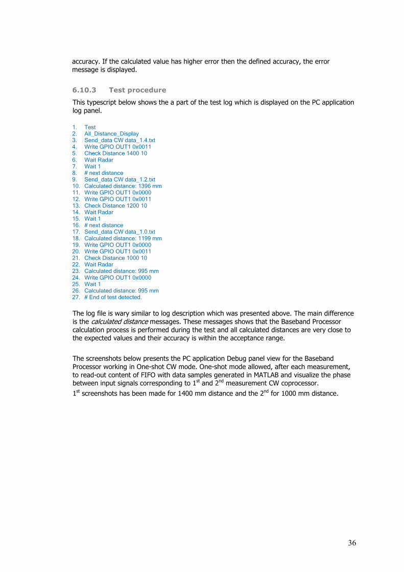
6.10.3 Test procedure
This typescript below shows the a part of the test log which is displayed on the PC application
log panel.
1. Test 2. All_Distance_Display 3. Send_data CW data_1.4.txt 4. Write GPIO OUT1 0x0011 5. Check Distance 1400 10 6. Wait Radar 7. Wait 1 8. # next distance 9. Send_data CW data_1.2.txt 10. Calculated distance: 1396 mm 11. Write GPIO OUT1 0x0000 12. Write GPIO OUT1 0x0011 13. Check Distance 1200 10 14. Wait Radar 15. Wait 1 16. # next distance 17. Send_data CW data_1.0.txt 18. Calculated distance: 1199 mm 19. Write GPIO OUT1 0x0000 20. Write GPIO OUT1 0x0011 21. Check Distance 1000 10 22. Wait Radar 23. Calculated distance: 995 mm 24. Write GPIO OUT1 0x0000 25. Wait 1 26. Calculated distance: 995 mm 27. # End of test detected.
The log file is wary similar to log description which was presented above. The main difference
is the calculated distance messages. These messages shows that the Baseband Processor
calculation process is performed during the test and all calculated distances are very close to the expected values and their accuracy is within the acceptance range.
The screenshots below presents the PC application Debug panel view for the Baseband
Processor working in One-shot CW mode. One-shot mode allowed, after each measurement,
to read-out content of FIFO with data samples generated in MATLAB and visualize the phase between input signals corresponding to 1st and 2nd measurement CW coprocessor.
1st screenshots has been made for 1400 mm distance and the 2nd for 1000 mm distance.

37
Figure 10. Debug panel view for CW mode, distance 1400 mm
Figure 11. Debug panel view for CW mode, distance 1000 mm
6.10.4 Test result
One shot CW radar mode test was executed successfully. No errors were found and all
calculated distances are within the margin of error are within the margin of error and this
confirms that the Baseband Processor is working properly in One shot CW mode.
38
6.11. One shot FMCW radar mode
6.11.1 Test description
The test validates the operational of the Baseband Processor in FMCW mode while One shot
mode is activated. The test validates the correctness of calculation of the distance between radar and target object. The calculation is based on the data generated in MATLAB. The
generated data emulate the operation of the analog part of the radar connected to Baseband
Processor by ADC interface.
Generation of data in MATLAB is based on FMCW algorithm a pre-defined value of distance to
the target. This distance calculated in the Baseband Processor must be consistent with value set during generation of MATLAB. Any differences may result from algorithm accuracy and
calculation precision. For each distance, it is defined in the test script, a maximum difference
between calculated distance and the actual distance.
6.11.2 Test scenario
The typescript below shows the a part of the test script which contains a validation of the two
distance calculations.
1. Write FMCW_PROC WINDOW 0x0001
2. Write FMCW_PROC WINDOW 0x01f4
3. Write FMCW_PROC WINDOW 0x0001
4. Write FMCW_PROC WINDOW 0x021c
5. …
6. Write FMCW_PROC WINDOW 0x0120
7. Write FMCW_PROC WINDOW 0x0001
8. Write FMCW_PROC WINDOW 0x00cc
9. Write FMCW_PROC WINDOW 0x0000
10. Write GPIO OUT1 0x0003
11. Send_data FMCW fmcwdata_1.5.txt
12. Wait Radar
13. Check Distance 1500 50
14. Wait 500
15. Check Distance OFF
16. # next distance
17. Send_data FMCW fmcwdata_1.2.txt
18. Wait Radar
19. Check Distance 1200 30
20. Wait 500
21. Check Distance OFF
In first lines (1 to 9) write command sends the 48 values which are the samples that are used
to define the Kaiser window. These samples were calculated by the PC Application and copied to the test script (this operation can be obtained by entering the number into the field next to
the FFT window button and then pressing it). The window function is necessary for FFT computation executed by Baseband Processor. The FFT computation is the part of FMCW
distance calculation.
At line nr 10 write command set the register OUT1 of the GPIO block. . The register OUT1 is used to start Baseband Processor operation in One-shot FMCW mode. At lines 11 and 17 data
samples generated in MATLAB are sent to Baseband Processor which starts calculation process. At lines 12 and 18 wait command causes waiting for Baseband Processor interrupt
39
which declares the end of the first calculation process. At lines 13 and 19 check distance command compares calculated values with expected values. The last number in this command
is the acceptable calculation accuracy. If the calculated value has higher error then the
defined accuracy, the error message is displayed. At lines 14 and 20 check distance off command causes that the PC application ends the compare operation before loading data
corresponding to next value of distance to a target.
6.11.3 Test procedure
This typescript below shows the a part of the test log which is displayed on the PC application
log panel.
1. Write FMCW_PROC WINDOW 0x0001
2. Write FMCW_PROC WINDOW 0x01f4
3. …
4. Write FMCW_PROC WINDOW 0x00cc
5. Write FMCW_PROC WINDOW 0x0000
6. Write GPIO OUT1 0x0003
7. Send_data FMCW fmcwdata_1.5.txt
8. All_Distance_Display
9. Wait Radar
10. Wait Radar
11. Check Distance 1500 50
12. Wait 500
13. Calculated distance: 1489 mm
14. Calculated distance: 1489 mm
15. …
16. Calculated distance: 1489 mm
17. Calculated distance: 1489 mm
18. Check Distance OFF
19. Send_data FMCW fmcwdata_1.2.txt
20. Wait Radar
21. Wait Radar
22. Check Distance 1200 30
23. Wait 500
24. Calculated distance: 1222 mm
25. Calculated distance: 1222 mm
26. …
27. Calculated distance: 1222 mm
28. Calculated distance: 1222 mm
29. Check Distance OFF
30. Send_data FMCW fmcwdata_1.1.txt
31. Wait Radar
32. Wait Radar
33. Check Distance 1100 45
34. Wait 500
35. Calculated distance: 1141 mm
36. Calculated distance: 1141 mm
37. …
38. Calculated distance: 1141 mm

40
39. Calculated distance: 1141 mm
40. Check Distance OFF
41. Send_data FMCW fmcwdata_1.0.txt
42. Wait Radar
43. Wait Radar
44. Check Distance 1000 20
45. Wait 500
46. Calculated distance: 998 mm
47. Calculated distance: 998 mm
48. …
49. Calculated distance: 998 mm
50. Calculated distance: 998 mm
51. Check Distance OFF
52. Calculated distance: 998 mm
53. Send_data FMCW fmcwdata_0.9.txt
54. Wait Radar
55. Calculated distance: 998 mm
56. Wait Radar
57. Check Distance 900 20
58. Wait 500
59. Calculated distance: 903 mm
60. Calculated distance: 903 mm
61. …
62. Calculated distance: 903 mm
63. Calculated distance: 903 mm
64. Check Distance OFF
65. Send_data FMCW fmcwdata_0.8.txt
66. Wait Radar
67. Wait Radar
68. Check Distance 800 20
69. Wait 500
70. Calculated distance: 819 mm
71. Calculated distance: 819 mm
72. …
73. Calculated distance: 819 mm
74. Calculated distance: 819 mm
75. Check Distance OFF
76. Send_data FMCW fmcwdata_0.7.txt
77. Wait Radar
78. Wait Radar
79. Check Distance 700 60
80. Wait 500
81. Calculated distance: 669 mm
82. Calculated distance: 669 mm
83. …
84. Calculated distance: 669 mm
85. Calculated distance: 669 mm
86. Check Distance OFF
87. Send_data FMCW fmcwdata_0.6.txt

41
88. Wait Radar
89. Wait Radar
90. Check Distance 600 45
91. Wait 500
92. Calculated distance: 644 mm
93. Calculated distance: 644 mm
94. …
95. Calculated distance: 644 mm
96. Calculated distance: 644 mm
97. Check Distance OFF
98. Send_data FMCW fmcwdata_0.5.txt
99. Wait Radar
100. Wait Radar
101. Check Distance 500 20
102. Wait 500
103. Calculated distance: 483 mm
104. Calculated distance: 483 mm
105. …
106. Calculated distance: 483 mm
107. Calculated distance: 483 mm
108. Check Distance OFF
109. Send_data FMCW fmcwdata_0.4.txt
110. Wait Radar
111. Wait Radar
112. Check Distance 400 25
113. Wait 500
114. Calculated distance: 424 mm
115. Calculated distance: 424 mm
116. …
117. Calculated distance: 424 mm
118. Calculated distance: 424 mm
119. Check Distance OFF
120. Write GPIO OUT1 0x0000
121. # End of test detected.
The log test is similar to the test script which was presented beforehand. The main difference
is the calculated distance messages. These messages shows that the Baseband Processor calculation process is performed during the test and all calculated distances are very close to
the expected values and their accuracy is within the acceptance range.
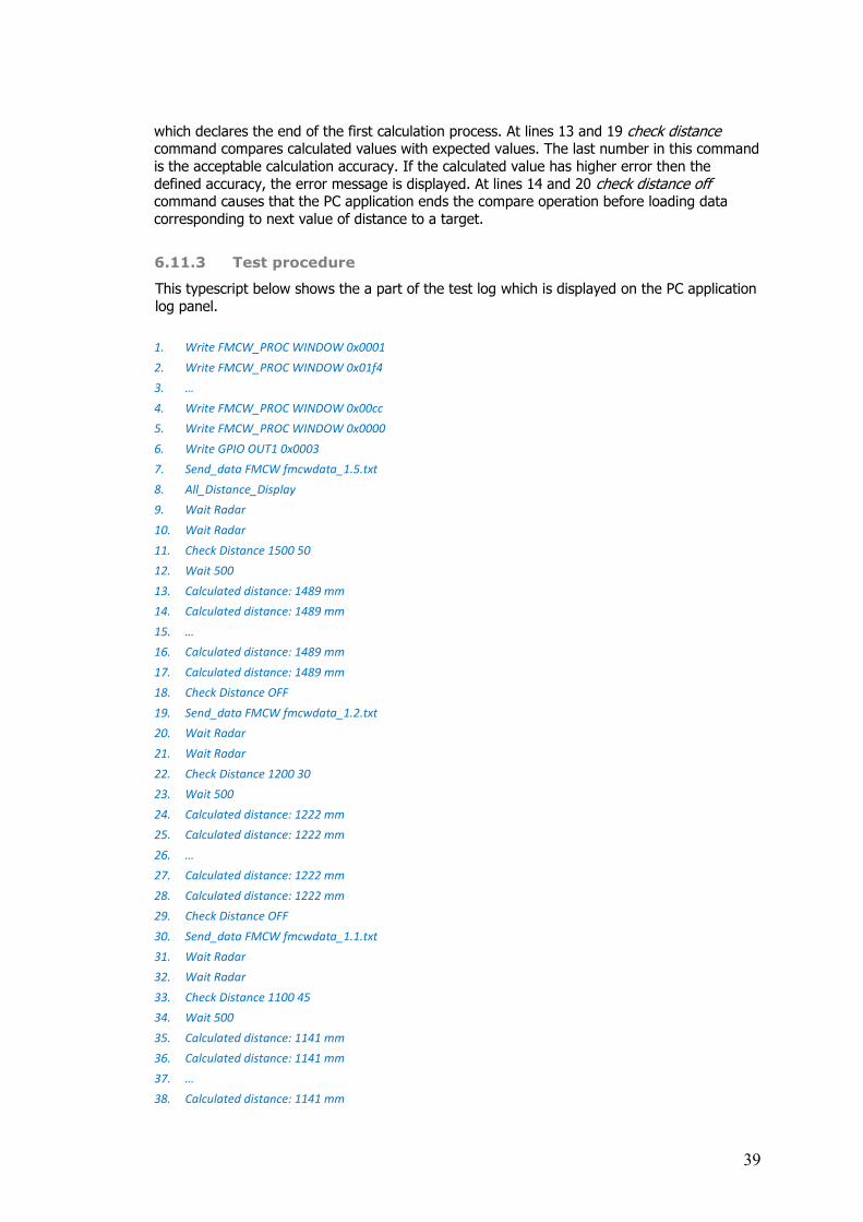
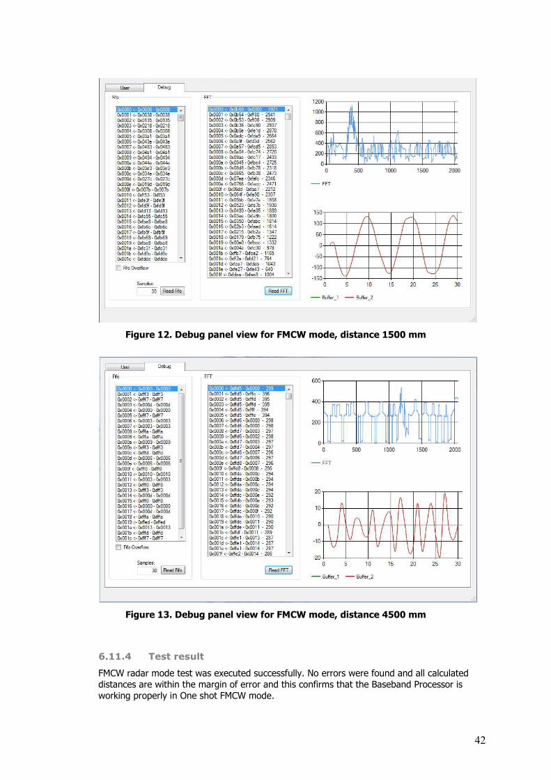
The screenshots below presents the PC application Debug panel view for the Baseband
Processor working in One-shot FMCW mode. One-shot mode allowed, after each measurement, to read-out content of FIFO with data samples generated in MATLAB and
visualize the input signal, which frequency is measured by FMCW coprocessor. Additionally raw FFT result can be read our from FMCW coprocessor and visualized in form of frequency
spectrum.
1st screenshots has been made for 1500 mm distance and the 2nd for 4500 mm distance.
42
Figure 12. Debug panel view for FMCW mode, distance 1500 mm
Figure 13. Debug panel view for FMCW mode, distance 4500 mm
6.11.4 Test result
FMCW radar mode test was executed successfully. No errors were found and all calculated
distances are within the margin of error and this confirms that the Baseband Processor is
working properly in One shot FMCW mode.

43
6.12. CW radar mode with not default configuration
6.12.1 Test description
The test validates the operational of the Baseband Processor in CW mode while configuration of the Baseband Processor is done by PC application. Starting the Baseband Processor in not
default configuration requires that the firmware skips the configuration process and not
overwrite the configuration done by PC application. That is achieved by NON-DEFAULT mode of operation which can be activated by the PC application while starting the Baseband
Processor.
6.12.2 Test scenario
The typescript below shows the a part of the test script which contains a validation of the two
distance calculations.
1. Write CW_PROC DELTA_FR_LOW 0xA8
2. Write CW_PROC DELTA_FR_HIGH 0x61
3. Write CW_PROC DISCARD_NUM_LOW 0x40
4. Write CW_PROC DISCARD_NUM_HIGH 0x00
5. Write CW_PROC I_DC_LOW 0x00
6. Write CW_PROC I_DC_HIGH 0x00
7. Write CW_PROC I_AMP_LOW 0x01
8. Write CW_PROC I_AMP_HIGH 0x00
9. Write CW_PROC Q_DC_LOW 0x00
10. Write CW_PROC Q_DC_HIGH 0x00
11. Write CW_PROC Q_AMP_LOW 0x01
12. Write CW_PROC Q_AMP_HIGH 0x00
13. Write CW_PROC AVER_NUM 0x0
14. Write AFE FREQ_HIGH 0x9D
15. Write AFE FREQ_LOW 0x56
16. Write AFE CTRL1 0x00
17. Write AFE CTRL2 0x04
18. Write PLL CLKDIV 0x02131415
19. Write PLL PHASE 0x02232425
20. Write PLL MOD 0x02333435
21. Write PLL FUNCTION 0x02434445
22. Write 0x230 0x30
23. Write 0x231 0x05
24. Write 0x232 0x00
25. Write 0x233 0x00
26. Write 0x234 0x70
27. Write 0x235 0x06
28. Write 0x236 0x00
29. Write 0x237 0x00
30. Send_data CW data_1.4.txt
31. Write GPIO OUT1 0x0005
32. Check Distance 1400 10
33. Wait Radar

44
34. …
At lines 1 and 21 PC application sets a desired configuration of the Baseband Processor. It performs write accesses to CW_RADAR coprocessor, Analog Front-end and PLL. Further, at
lines 22 to 29 it writes to XRAM value of desired frequency settings that are to be used by
Baseband Processor while swiching PLL from 1st to 2nd measurement. Finally, at line 30 data samples generated in MATLAB are sent to Baseband Processor and, at line 31, the Baseband
Processor is activated in NON-DEFAULT mode. Last step of test procedure is to check the distance calculated by the Baseband Processor, which is done at lines 32, 33. If the calculated
value has higher error then the defined accuracy, the error message is displayed.
6.12.3 Test result
CW radar mode with not default parameters test was executed successfully. No errors were found and all calculated distances are within the margin of error are within the margin of error
and this confirms that the Baseband Processor is working properly in CW mode with not default configuration.
6.13. FMCW radar mode with not default configuration
6.13.1 Test description
The test validates the operational of the Baseband Processor in FMCW mode while
configuration of the Baseband Processor is done by PC application. Starting the Baseband Processor in not default configuration requires that the firmware skips the configuration
process and not overwrite the configuration done by PC application. That is achieved by NON-DEFAULT mode of operation which can be activated by the PC application while starting the
Baseband Processor.
6.13.2 Test scenario
The typescript below shows the a part of the test script which contains a validation of the two distance calculations.
1. All_Distance_Display
2. Write FMCW_PROC WINDOW 0x0001
3. Write FMCW_PROC WINDOW 0x01f4
4. …
5. Write FMCW_PROC WINDOW 0x00cc
6. Write FMCW_PROC WINDOW 0x0000
7. Write FMCW_PROC SFREQ_LOW 0x64
8. Write FMCW_PROC SFREQ_HIGH 0x00
9. Write FMCW_PROC SCALLING_LOW 0x01
10. Write FMCW_PROC SCALLING_MID 0x21
11. Write FMCW_PROC SCALLING_HIGH 0x22
12. Write FMCW_PROC RAMP_T_LOW 0xD0
13. Write FMCW_PROC RAMP_T_HIGH 0x07
14. Write FMCW_PROC RAMP_F_LOW 0xCC
15. Write FMCW_PROC RAMP_F_HIGH 0x04
16. Write FMCW_PROC LOWEST_BIN_LOW 0x05
17. Write FMCW_PROC LOWEST_BIN_HIGH 0x00
18. Write FMCW_PROC SAMPLE_NUM_LOW 0x30

45
19. Write FMCW_PROC SAMPLE_NUM_HIGH 0x00
20. Write FMCW_PROC FR_SPACE 0x02
21. Write FMCW_PROC DISCARD 0x01
22. Write FMCW_PROC FMCW_AVER_NUM 0x00
23. Send_data FMCW fmcwdata_1.5.txt
24. Write GPIO OUT1 0x0007
25. Check Distance 1500 50
26. Wait Radar
27. …
At lines 1 and 22 PC application sets a desired configuration of the Baseband Processor. It
performs write accesses to FMCW_RADAR coprocessor, including definition of window function that is to be applied before FFT computation. Further, 23 data samples generated in MATLAB
are sent to Baseband Processor and, at line 24, the Baseband Processor is activated in NON-
DEFAULT mode. Last step of test procedure is to check the distance calculated by the Baseband Processor, which is done at lines 25, 26. If the calculated value has higher error
then the defined accuracy, the error message is displayed.
6.13.3 Test result
FMCW radar mode with not default parameters test was executed successfully. No errors were
found and all calculated distances are within the margin of error are within the margin of error
and this confirms that the Baseband Processor is working properly in FMCW mode with not default configuration.
46
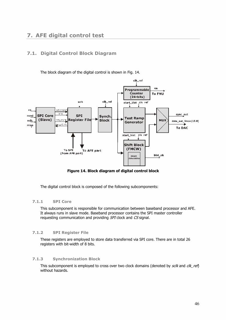
7. AFE digital control test
7.1. Digital Control Block Diagram
The block diagram of the digital control is shown in Fig. 14.
Figure 14. Block diagram of digital control block
The digital control block is composed of the following subcomponents:
7.1.1 SPI Core
This subcomponent is responsible for communication between baseband processor and AFE.
It always runs in slave mode. Baseband processor contains the SPI master controller requesting communication and providing SPI clock and CS signal.
7.1.2 SPI Register File
These registers are employed to store data transferred via SPI core. There are in total 26
registers with bit-width of 8 bits.
7.1.3 Synchronization Block
This subcomponent is employed to cross over two clock domains (denoted by sclk and clk_ref) without hazards.

47
7.1.4 Programmable Counter
This subcomponent (timer) provides an enable signal for frequency measurement. The enable
signal is active within time interval programmable via SPI interface.
7.1.5 Test Ramp Generator
This subcomponent is able to generate a frequency ramp with three different time periods, but with pre-determined values of frequency ramp. The purpose is to have an opportunity for DAC testing without programming a RAM memory cell in Shift Block.
7.1.6 Shift Block
This subcomponent is used for storing frequency ramp values sent by baseband processor and transferred via SPI interface. For storing those values, a RAM memory cell with size 256x16 bits is employed.
7.2. Digital Control Pin Description
The table bellow summarizes pin description of the digital control.
Table 8. Pin Description of Digital Control
Name Type
Polarity
or
Bus
Size
Description
nres In Low Hardware reset input
clk_ref In Rise Reference clock, currently is set to
50 MHz
sclk In Rise and
Fall
SPI clock (SPI interface)
cs In Low Chip Select (SPI interface)
mosi In Level Master-Output-Slave-Input (SPI
interface)
miso Out Level Master-Input-Slave-Output (SPI interface)
start_bist In High Start signal of BIST SRAM memory
bist_ok Out High Pass/Fail signal of BIST SRAM memory
en Out High Enable signal for frequency
measurement unit (FMU)
data0_fmu In 8 Higher - (23:16) bits of frequency

48
measured by FMU
data1_fmu In 8 Middle - (15:8) bits of frequency measured by FMU
data2_fmu In 8 Lower - (7:0) bits of frequency measured by FMU
data_out_fmcw Out 16 Signal frequency value sent to DAC
sync_out Out High Start of frequency ramp indicated
by rising edge
vco_coarse In 3 VCO coarse value
power_amp Out 3 Power amplifier value
power_det1 Out 2 Power detector value 1
power_det2 Out 2 Power detector value 2
temp_sensor Out 4 Temperature sensor value
vga_stage1 Out 8 VGA value 1
vga_stage2 Out 8 VGA value 2
vga_stage3 Out 8 VGA value 3
vga_stage4 Out 8 VGA value 4
data1_rd In 8 General purpose inputs
data2_rd In 8 General purpose inputs
data1_out Out 8 General purpose outputs
data2_out Out 8 General purpose outputs
data3_out Out 8 General purpose outputs
data4_out Out 8 General purpose outputs
data5_out Out 8 General purpose outputs
7.3. SPI Register Map
The table bellow presents a SPI register map. Bit-width of each register is 8 bits. The number of
writable and readable registers is 18 and 8, respectively, what is in total 26 registers.
Table 9. SPI Register Map
Address(4:0) Access Description
00000 Write (7 : 2) – Higher (11 : 6) bits of programmable ratio R in FMCW mode;
(1 : 0) - Higher (7 : 6) bits of number of frequency points in FMCW mode;
00001 Write FMCW mode:
(7) – writing/reading mode bit; Logic ‘1’ - writing mode; Logic ‘0’ - reading mode;
(6 : 1) bits
Writing mode : lower (5:0) bits of number of frequency points;
Reading mode : lower (5:0) bits of programmable clock ratio R;
(0) - freeze bit ;
49
In reset state, as long as FMCW mode bit is ‘0’, freeze bit (low active) prevents reading unknown
values from memory and delivering those unknown
values to DAC;
00010 Write FMCW mode : Higher - (15:8) bits of a signal
frequency;
00011 Write FMCW mode : Lower - (7:0) bits of a signal frequency
00100 Write Higher - (23:16) bits of programmable counter used
for frequency measurement
00101 Write Middle - (15:8) bits of programmable counter used for FMU
00110 Write Lower - (7 :0) bits of programmable counter for FMU
00111 Write (7:5) bits - VCO coarse value
(4:2) bits - Power Amplifier value;
(1:0) bits – selecting bits for frequency ramp period in
test mode;
01000 Write VGA stage 1 value
01001 Write VGA stage 2 value
01010 Write VGA stage 3 value
01011 Write VGA stage 4 value
01100 Write Memory address in test mode
01101 Write data1_out value
01110 Write data2_out value
01111 Write data3_out value
10000 Write data4_out value
10001 Write data5_out value
10010 Read (7:6) bits – Power detector 1 value
(5:4) bits – Power detector 2 value
(3:0) bits – Temp. sensor value
10011 Read Higher – (23:16) bits of frequency measured by FMU
10100 Read Middle – (15:8) bits of frequency measured by FMU
10101 Read Lower – (7:0) bits of frequency measured by FMU
10110 Read data1_rd value
10111 Read data2_rd value
11000 Read Higher – (15 :8) bits of memory cell output in test mode
11001 Read Lower – (7:0) bits of memory cell output in test mode
7.4. 1.4 Digital Control Functionality
In general, the digital control of AFE can work in two modes : normal and test mode. First,
the data communication protocol of SPI interface will be described.
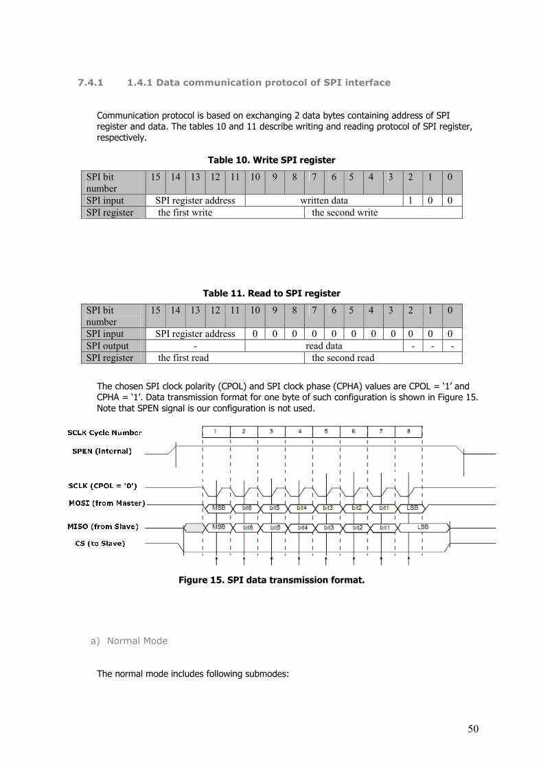
50
7.4.1 1.4.1 Data communication protocol of SPI interface
Communication protocol is based on exchanging 2 data bytes containing address of SPI register and data. The tables 10 and 11 describe writing and reading protocol of SPI register,
respectively.
Table 10. Write SPI register
SPI bit
number
15 14 13 12 11 10 9 8 7 6 5 4 3 2 1 0
SPI input SPI register address written data 1 0 0
SPI register the first write the second write
Table 11. Read to SPI register
SPI bit
number
15 14 13 12 11 10 9 8 7 6 5 4 3 2 1 0
SPI input SPI register address 0 0 0 0 0 0 0 0 0 0 0
SPI output - read data - - -
SPI register the first read the second read
The chosen SPI clock polarity (CPOL) and SPI clock phase (CPHA) values are CPOL = ‘1’ and CPHA = ‘1’. Data transmission format for one byte of such configuration is shown in Figure 15.
Note that SPEN signal is our configuration is not used.
Figure 15. SPI data transmission format.
a) Normal Mode
The normal mode includes following submodes:
51
• In FMCW radar mode, the digital control is responsible for receiving the frequency
ramp values generated by the baseband processor. Then, those frequency ramp values are fed to the DAC. The time period of the frequency ramp defined by
programmable ratio R as well as the number of frequency points within one ramp is
programmable via SPI interface.
• Configuration of the various signal values required for functioning of the AFE.
• Reading and transferring a signal frequency value measured by Frequency
Measurement Unit (FMU) of AFE to baseband processor.
b) Test Mode
The test mode includes following submodes:
• Frequency ramp generation dedicated for DAC testing without programming a RAM
memory cell. The values of frequency ramp are pre-determined and cannot be changed. On the other hand, the time period of frequency ramp can be
programmable including 500 µs, 1 ms and 2 ms frequency ramps. For default ramp of 500 µs time period, SPI is not used as well, only BIST input signal (denoted as
start_bist) shall be activated. For others two frequency ramps (1 ms and 2 ms),
besides activation of BIST input signal, two bits of the appropriate SPI register (with address “00111”) shall be programmable as shown in table 12.
Table 12. Programming the frequency ramp for DAC testing
start_bist SPI reg. with addr. (“00111”), bits (1:0)
500 µs- frequency ramp
‘1’ “00”
1 ms –
frequency ramp
‘1’ “01”
2 ms – frequency ramp
‘1’ “10”/”11”
• BIST test for the RAM cell. To start this test, BIST input signal shall be activated. A
random pre-determined sequence is stored in memory and afterwards every memory location is read out to check its correctness. When test is finished, the data
correctness shall be indicated by asserting bist_ok pin to high.
• During programming of the RAM cell (in FMCW radar mode) the frequency ramp
values are stored in memory. In order to check whether correct value is written in the
memory, every memory location can be read via SPI interface.
7.5. Test results of the first chip version
The first version of the ASIC chip including the simplified digital control as well as AFE has been taped out in august 2010. The AFE is also simplified and includes only VCO, DAC and
FMU. As SPI master controller, we have used SPI Aardwark controller with appropriate

52
software under Linux PC. The test results are summarized in Table 13. The diagram flow of test procedures is given in Figure 16.
Table 13. Test results of the first chip version
Test Pass/Fail
SPI functionality Pass
Frequency measurement Pass
Memory BIST Pass
Memory programming and
frequency ramp generation
Fail
DAC test Pass
Basically, the tests of SPI functionality and frequency measurement have been passed, but with some bugs which have been discovered and corrected in new chip version. Memory
programming and frequency ramp generation have been failed. Possible cause is a
synchronization problem between SPI and reference clock signal. This issue has been also improved in new chip version.
Figure 16. Diagram flow of test procedures.


![Silicon-based solar cells - fotowoltaika.edu.pl. Thin-layer cells and modules ... Silicon -based solar cells – characteristics and production processes ] ] Silicon -based solar cells](https://static.fdocuments.net/doc/165x107/5b0c5ceb7f8b9a6a6b8c3d79/silicon-based-solar-cells-thin-layer-cells-and-modules-silicon-based-solar.jpg)