
Investigating Silicon-Based Photoresists with Coherent...
112
Investigating Silicon-Based Photoresists with Coherent Anti-Stokes Raman Scattering and X-ray Micro-spectroscopy by Allison G. Caster A dissertation submitted in partial satisfaction of the requirements for the degree of Doctor of Philosophy in Chemistry in the Graduate Division of the University of California, Berkeley Committee in charge: Professor Stephen R. Leone, Chair Professor Richard Mathies Professor Luke P. Lee Spring 2010
Transcript of Investigating Silicon-Based Photoresists with Coherent...

Investigating Silicon-Based Photoresists with
Coherent Anti-Stokes Raman Scattering and X-ray Micro-spectroscopy
by
Allison G. Caster
A dissertation submitted in partial satisfaction of the requirements for the degree of
Doctor of Philosophy
in
Chemistry
in the
Graduate Division
of the
University of California, Berkeley
Committee in charge:
Professor Stephen R. Leone, Chair
Professor Richard Mathies
Professor Luke P. Lee
Spring 2010

1
Abstract
Investigating Silicon-Based Photoresists with
Coherent Anti-Stokes Raman Scattering and X-ray Micro-spectroscopy
by
Allison G. Caster
Doctor of Philosophy in Chemistry
University of California, Berkeley
Professor Stephen R. Leone, Chair
Photoresist lithography is a critical step in producing components for high-density data storage
and high-speed information processing, as well as in the fabrication of many novel micro and
nanoscale devices. With potential applications in next generation nanolithography, the chemistry
of a high resolution photoresist material, hydrogen silsesquioxane (HSQ), is studied with two
different state-of-the-art, chemically selective microscope systems. Broadband coherent anti-
Stokes Raman scattering (CARS) micro-spectroscopy and scanning transmission Xray
microscopy (STXM) reveal the rate of the photoinduced HSQ cross-linking, providing insight
into the reaction order, possible mechanisms and species involved in the reactions.
Near infrared (NIR) multiphoton absorption polymerization (MAP) is a relatively new technique
for producing sub-diffraction limited structures in photoresists, and in this work it is utilized in
HSQ for the first time. By monitoring changes in the characteristic Raman active modes over
time with ~500 ms time resolution, broadband CARS micro-spectroscopy provides real-time, in
situ measurements of the reaction rate as the HSQ thin films transform to a glass-like network
(cross-linked) structure under the focused, pulsed NIR irradiation. The effect of laser power and
temporal dispersion (chirp) on the cross-linking rate are studied in detail, revealing that the
process is highly non-linear in the peak power of the laser pulses, requiring ~6 photons (on
average) to induce each cross-linking event at high laser power, which opens the possibility for
high resolution MAP lithography of HSQ. Reducing the peak power of the laser pulses, by
reducing average laser power or increasing the chirp, allows fine control of the HSQ cross-
linking rate and effective halting of the cross-linking reaction when desired, such that broadband
CARS spectra can also be obtained without altering the material.
Direct-write Xray lithography of HSQ and subsequent high resolution STXM imaging of line
patterns reveals a dose and thickness dependent spread in the cross-linking reaction of greater
than 70 nm from the exposed regions for 300 nm to 500 nm thick HSQ films. This spread leads
to proximity effects such as area dependent exposure sensitivity. Possible mechanisms
responsible for the reaction spread are presented in the context of previously reported results.
Xray lithography and imaging is also used to assess the Xray induced cross-linking rate, and
similarities are observed between NIR MAP and Xray induced network formation of HSQ.

i
This dissertation is dedicated to my parents –
who always encouraged me to ask “Why?”

ii
Contents
1 INTRODUCTION .............................................................................................................................................. 1
1.1 THE IMPORTANT ROLE OF PHOTORESISTS .................................................................................................... 1 1.2 HYDROGEN SILSESQUIOXANE (HSQ) RESISTS ............................................................................................. 3 1.3 MULTIPHOTON ABSORPTION POLYMERIZATION ........................................................................................... 4 1.4 MICROSPECTROSCOPY OF PHOTORESISTS .................................................................................................... 5
1.4.1 Coherent anti-Stokes Raman scattering microscopy ............................................................................. 5 1.4.2 Scanning transmission X-ray microscopy .............................................................................................. 6
1.5 OUTLINE: OPTIMIZING MICROSPECTROSCOPY TECHNIQUES TO STUDY HSQ CHEMISTRY ............................ 7
2 EXPERIMENTAL TECHNIQUES: THEORY AND DESIGN .................................................................... 9
2.1 COHERENT ANTI-STOKES RAMAN SCATTERING (CARS) ............................................................................. 9 2.2 SINGLE-BEAM, BROADBAND CARS MICROSCOPY ..................................................................................... 13
2.2.1 Double Quadrature Spectral Interferometry (DQSI) CARS ................................................................ 13 2.2.2 Pulse Shaping and Compression with a Spatial Light Modulator ....................................................... 19
2.3 NEAR EDGE X-RAY ABSORPTION FINE STRUCTURE (NEXAFS) SPECTROSCOPY ........................................ 24 2.4 SCANNING TRANSMISSION X-RAY MICROSCOPY (STXM) ......................................................................... 28
3 OBSERVING MULTIPHOTON CROSS-LINKING OF HSQ WITH BROADBAND CARS ................ 34
3.1 INTRODUCTION: NEAR INFRARED MULTIPHOTON ABSORPTION POLYMERIZATION OF HSQ ....................... 34 3.2 SAMPLE PREPARATION AND EXPERIMENTAL SETUP ................................................................................... 35 3.3 MEASURING REAL-TIME CROSS-LINKING KINETICS ................................................................................... 35 3.4 SPONTANEOUS RAMAN SPECTRA AND DEPOLARIZATION RATIOS OF HSQ THIN FILMS .............................. 41 3.5 CONCLUSIONS ........................................................................................................................................... 46
4 INVESTIGATING THE NEAR-IR MULTIPHOTON CROSS-LINKING MECHANISM OF HSQ .... 47
4.1 INTRODUCTION .......................................................................................................................................... 47 4.2 SAMPLE PREPARATION AND EXPERIMENTAL SETUP ................................................................................... 48 4.3 DEPENDENCE OF CROSS-LINKING RATE ON PEAK INTENSITY: CHIRP EFFECTS ............................................ 49 4.4 NON-LINEAR POWER DEPENDENCE OF CROSS-LINKING RATE ..................................................................... 51 4.5 A CLOSER LOOK AT POTENTIAL CROSS-LINKING MECHANISMS AND REACTION ORDER .............................. 58 4.6 CONCLUSIONS ........................................................................................................................................... 63
5 PROBING HSQ CROSS-LINKING CHEMISTRY ON THE NANOSCALE ........................................... 65
5.1 INTRODUCTION: STXM AND X-RAY LITHOGRAPHY OF HSQ .................................................................... 65 5.2 SAMPLE PREPARATION AND EXPERIMENTAL SETUP................................................................................... 66 5.3 OXYGEN AND SILICON K-EDGE NEXAFS SPECTRA OF X-RAY EXPOSED HSQ .......................................... 70 5.4 X-RAY INDUCED CROSS-LINKING REACTION RATE ..................................................................................... 74 5.5 AREA DEPENDENT SENSITIVITY ................................................................................................................. 76 5.6 QUANTIFYING REACTION SPREAD .............................................................................................................. 80 5.7 POTENTIAL MECHANISMS FOR CROSS-LINKING REACTION SPREAD ............................................................ 83 5.8 CONCLUSIONS ........................................................................................................................................... 85
6 CONCLUSIONS .............................................................................................................................................. 87
6.1 PRELIMINARY RESULTS: INCORPORATING ADDITIVES TO REDUCE REACTION SPREAD ............................... 87 6.2 SUMMARY AND OUTLOOK: HSQ PHOTOLITHOGRAPHY ............................................................................. 90
BIBLIOGRAPHY

iii
List of Figures
FIGURE 1.1 SIDE-VIEW SCHEMATIC OF SELECT RESIST PROCESSING STEPS FOR A NEGATIVE-TONE RESIST. .................... 2 FIGURE 1.2 SCHEMATIC OF HSQ (A) CAGE (MONOMER) AND (B) POSSIBLE PARTIAL NETWORK STRUCTURE
(OLIGOMER) FORMED BY CROSS-LINKING TWO MONOMER CAGES. IN SOLUTION, THE MOLECULAR STRUCTURE IS
ACTUALLY COMPRISED OF OLIGOMERS OF VARIOUS SIZES.2 .................................................................................. 3
FIGURE 2.1 SCHEMATIC OF (A) RAMAN AND (B) CARS PROCESSES ............................................................................. 10 FIGURE 2.2 SCHEMATIC OF (A) NARROWBAND VS (B) BROADBAND CARS PROCESSES................................................. 12 FIGURE 2.3 DQSI CARS EXPERIMENTAL SETUP. ......................................................................................................... 14 FIGURE 2.4 (A) SCHEMATIC TOP VIEW OF PULSE SHAPER, WITH SLM AT CENTER. (B) TOP VIEW PHOTOGRAPH OF PULSE
SHAPER. NOTE THAT THE DISPERSED BEAM PASSES OVER THE TOP OF THE SMALL ENTRANCE AND EXIT MIRRORS.
........................................................................................................................................................................... 15 FIGURE 2.5 DQSI CARS DETECTION SCHEME,
107-108 SHOWING (A) POLARIZATION OF INCIDENT FIELDS AND DETECTED
SIGNALS, (B) TOTAL SIGNAL FROM TOLUENE FOR EACH SPECTRUM AND (C) DIFFERENCE OF TWO SIGNALS. ....... 17 FIGURE 2.6 DQSI-CARS SPECTRA OF (A) PS AND (B) PMMA, ACQUIRED IN 10 MS EACH. (C) DQSI CARS SPECTRAL
IMAGE OF A SELF-SEGREGATED PMMA/PS BLEND, ACQUIRED IN 3.5 MINUTES.108, 110
........................................ 19 FIGURE 2.7 (A) PHOTOGRAPH OF SLM (FRONT), WITH DASHED LINE AROUND ENTRANCE POLARIZER. (B) CLOSE UP OF
ENTRANCE POLARIZER, SHOWING FAINT BACK REFLECTION OF BROADBAND LASER SPECTRUM. ........................ 20 FIGURE 2.8 SCHEMATIC REPRESENTATION OF SLM LIQUID CRYSTAL (LC) MASKS AND POLARIZERS, (A) TOP VIEW AND
(B) FRONT PERSPECTIVE VIEW. BOLD BLACK ARROWS REPRESENT THE OPTICAL AXIS OF THE INDIVIDUAL LC
MOLECULES WITHIN EACH MASK. FOR DQSI CARS, THE EXIT POLARIZER IS REMOVED COMPLETELY. ............. 21 FIGURE 2.9 FRONT VIEW SCHEMATIC OF LIQUID CRYSTAL (LC) MASK, SHOWING ORIENTATION OF INCOMING LIGHT
POLARIZATION AND ITS ORTHOGONAL COMPONENTS WITH RESPECT TO LC OPTICAL AXES. ............................... 21 FIGURE 2.10 SCHEMATIC DIAGRAM OF A BIREFRINGENT CRYSTAL BASED HALF-WAVE PLATE, SHOWING 90° ROTATION
OF INCIDENT LIGHT POLARIZATION (RED) BY INTRODUCING A 180° PHASE SHIFT BETWEEN OF THE EX (BLUE) AND
EY (GREEN) COMPONENTS. AS IN THE SLM, THE INCIDENT LIGHT HERE IS POLARIZED AT 45 DEGREES WITH
RESPECT TO THE OPTICAL AXIS OF THE CRYSTAL.112
........................................................................................... 22 FIGURE 2.11 SIMPLIFIED SCHEMATIC OF NEAR-EDGE X-RAY ABSORPTION PROCESS, SHOWING POSSIBLE TRANSITIONS
TO THE LOWEST UNOCCUPIED MOLECULAR ORBITAL (LUMO), CONTINUUM AND QUASI-BOUND MO.117
........... 25 FIGURE 2.12 SCHEMATIC OF X-RAY INDUCED CORE ELECTRON TRANSITIONS.
4 (A) SINGLE-PHOTON IONIZATION OF 1S
ELECTRON, WHICH IS FOLLOWED BY (B) FLUORESCENCE EMISSION OR (C) NON-RADIATIVE AUGER DECAY........ 26 FIGURE 2.13 REPRESENTATIVE OXYGEN K-EDGE NEXAFS SPECTRUM OF HSQ THIN FILM, WITH GAUSSIAN PEAK
FITTING. PLACEMENT OF SHARP ABSORPTION EDGE “JUMP” IS APPROXIMATE..................................................... 28 FIGURE 2.14 OVERVIEW SCHEMATIC OF 5.3.2 STXM. ................................................................................................. 29 FIGURE 2.15 PHOTOGRAPHS OF STXM 5.3.2. (A) MICROSCOPE VACUUM CHAMBER. (B) MICROSCOPE COMPONENTS.
(C) CLOSE UP OF AREA WHERE THE SAMPLE HOLDER (FIGURE 2.17) IS MOUNTED DIRECTLY IN FRONT OF THE
PHOSPHOR-COATED TIP OF THE LUCITE LIGHT PIPE. ............................................................................................ 29 FIGURE 2.16 SCHEMATIC OF ZONE PLATE (A) FRONT VIEW AND (B) SIDE VIEW, SHOWING OSA AND POSITION OF FOCUS
FOR DIFFERENT DIFFRACTION ORDERS. THE FIRST ORDER FOCUS IS USED FOR STXM IMAGING, WITH THE
SAMPLE POSITIONED PERPENDICULAR TO THE BEAM AXIS AND PRECISELY AT THE FOCUS. ................................. 31 FIGURE 2.17 TWO VIEWS, (A) AND (B), OF THE SILICON NITRIDE SUBSTRATE, A 5X5 MM, 525 ΜM THICK FRAME WITH
1X1 MM, 100 NM THICK MEMBRANE WINDOW AT CENTER, COATED WITH HSQ THIN FILM. (C) SUBSTRATES
TAPED TO THE SAMPLE HOLDER PLATE FOR THE 5.3.2 STXM. ............................................................................ 32 FIGURE 2.18 EXAMPLE STXM FOCUS SCAN. (A) NEARLY FOCUSED IMAGE (550 EV) OF 100 NM AU NANOPARTICLES
AND CLUSTERS ON HSQ FILM SURFACE. BOLD BLACK ARROW POINTS TO POSITION OF 1D LINE SCAN (WHITE
LINE, DRAWN IN). (B) RESULTING FOCUS SCAN ACROSS 1D LINE AS ZONE-PLATE-TO-SAMPLE DISTANCE IS
VARIED. BLACK ARROWS INDICATE THE RELATIVE ZONE-PLATE-TO-SAMPLE DISTANCE FOR OPTIMAL FOCUSING.
........................................................................................................................................................................... 33 FIGURE 3.1 DQSI CARS SPECTRA OF HSQ THIN FILMS. (A) TEMPERATURE DEPENDENCE OF CROSS-LINKING. (B)
REAL-TIME MONITORING OF CROSS-LINKING IN FOCUSED, PULSED NEAR IR LASER BEAM. ................................. 37 FIGURE 3.2 SPONTANEOUS RAMAN SPECTRA OF HSQ THIN FILMS BAKED FOR 10 MINUTES AT 150 °C OR 350 °C. ..... 38 FIGURE 3.3 DECAY OF THE 562 CM
-1 PEAK AREA (CAGE-LIKE O-SI-O BEND) WITH TIME IN THE FOCUSED NEAR IR
BEAM, AND GROWTH OF THE 484 CM-1
BAND (NETWORK-LIKE SYMMETRIC STRETCH). SOLID LINES

iv
ARE DOUBLE EXPONENTIAL DECAY FIT. BOTH THE DECAY AND GROWTH KINETICS EXHIBIT A FAST FIRST STAGE
WITH A TIME CONSTANT OF ~24 S AND A MUCH SLOWER SECOND STAGE. ........................................................... 40 FIGURE 3.4 (A) FULL DQSI CARS SPECTRUM, 0.5 S ACQUISITION TIME AND (B) RAMAN SPECTRUM OVER THE SAME
SPECTRAL RANGE, 50 SECONDS ACQUISITION TIME. ............................................................................................ 42 FIGURE 3.5 SPONTANEOUS RAMAN SPECTRA OF ~1 ΜM THICK HSQ FILM PRE-BAKED AT 150 °C FOR 10 MINUTE. (A)
REGION ACCESSIBLE WITH DQSI CARS, AND (B) FULL SPECTRUM. ALL SCATTERED POLARIZATIONS ARE
DETECTED FOR THE UPPER CURVES (BLACK), BUT POLARIZED SIGNAL ONLY IS DETECTED FOR THE MIDDLE
CURVES (RED), AND THE BOTTOM CURVES (BLUE) ARE THE DEPOLARIZED SPECTRA. .......................................... 43 FIGURE 4.1 DECAY IN 562 CM
-1 PEAK AREA FOR A CHIRPED PULSE (UPPER CURVE, OPEN SQUARES) VERSUS
COMPRESSED PULSE (LOWER CURVE, FILLED CIRCLES) AT THE FOCUS IN THE HSQ THIN FILM, (A) RAW DATA,
BEFORE NORMALIZATION AND (B) NORMALIZED DATA, SHOWING EXPONENTIAL DECAY FIT CURVES WITH > 100X
FASTER CROSS-LINKING RATE WHEN THE CHIRP IS COMPRESSED. ....................................................................... 50 FIGURE 4.2 NORMALIZED DECAY IN THE PEAK AREA FOR THE CAGE-LIKE HSQ BAND AT 562 CM
-1 AT DIFFERENT
LASER POWERS FOR (A) DATA SET 1, WITH SLIGHT CHIRP, AND (B) DATA SET 2, WITH OPTIMAL CHIRP
COMPRESSION. THE NORMALIZED PEAK AREA IS EQUIVALENT TO THE RELATIVE DEGREE OF HSQ CROSS-
LINKING (EQ. 4.7). A STRONG INCREASE IN CROSS-LINKING RATE IS OBSERVED WITH INCREASING LASER POWER
IN BOTH SET 1 AND SET 2. FOR CLARITY, SINGLE EXPONENTIAL DECAY FIT CURVES ARE SHOWN ALONE IN (C)
FOR DATA SET 1 AND (D) FOR DATA SET 2. THE BETTER COMPRESSION IN SET 2 RESULTS IN SLIGHTLY HIGHER
PEAK POWER AND THEREFORE SLIGHTLY HIGHER CROSS-LINKING RATES AT THE SAME AVERAGE POWERS. ....... 52 FIGURE 4.3 HSQ CROSS-LINKING LIFETIME VERSUS LASER POWER. (A) FULL RANGE OF MEASUREMENTS, INSET IS
ZOOMED IN TO HIGH POWERS ONLY, AND ERROR BARS ARE ENCOMPASSED BY SIZE OF DATA MARKERS WHERE
NOT VISIBLE. (B) NATURAL LOG FORM OF DATA FOLLOWING EQ. 4.12, ERROR BARS NOT SHOWN. BEST FIT
LINES REVEAL A THRESHOLD FOR CROSS-LINKING ABOVE WHICH AN AVERAGE OF ~6±1 PHOTONS IS REQUIRED
PER CROSS-LINKING EVENT. ................................................................................................................................ 55 FIGURE 4.4 POSSIBLE REDISTRIBUTION MECHANISM INDUCED BY DIRECT, PHOTOLYTIC BOND CLEAVAGE. ...... 60 FIGURE 4.5 SCHEMATIC REPRESENTATION OF THE PROPOSED 4-CENTERED INTERMEDIATE OF THE REDISTRIBUTION
REACTION, SHOWN (A) IN THE PLANE OF THE PAGE, WHERE R REPRESENTS ANY INTERCONNECTED SPECIES,129
AND (B) IN A SLIGHTLY MORE REALISTIC GEOMETRY, WHICH SHOWS POSSIBLE INTERCONNECTED SPECIES FOR
THE FIRST CROSS-LINKING EVENT. ...................................................................................................................... 62 FIGURE 4.6 SCHEMATIC REPRESENTATION OF SILSESQUIOXANE CAGE STRUCTURE AND COMPARING TWO POSSIBLE
NETWORK STRUCTURES FORMED BY A SINGLE HSQ CROSS-LINKING EVENT. ΔE REPRESENTS ENERGY FROM
EITHER AN ELECTRON BEAM, LIGHT (XRAYS, EUV, ULTRAFAST PULSES), OR HEAT. THE UPPER PATHWAY
REPRESENTS THE PRIMARY MECHANISM PROPOSED FOR THERMALLY INDUCED CROSS-LINKING FROM ~190-
330 °C,36, 129
WHILE THE LOWER IS THE MAIN MECHANISM PROPOSED IN THE LITERATURE FOR E-BEAM
EXPOSURE37
AND HEATING ABOVE 400 °C.36, 129
THE SPIN-ON SOLUTION OF HSQ (DOW CORNING FOX®)
CONTAINS A MIXTURE OF CAGES AND OLIGOMERS OF HSQ. ............................................................................... 63 FIGURE 5.1 (A) APPROXIMATE X-RAY BEAM PROFILE. (B) SIMULATED DIRECT-WRITE X-RAY LITHOGRAPHY PATTERN
FOR SINGLE-PASS LINE WITH 50 NM POINT SPACING AND NORMALIZED BEAM PROFILE. (C) SIMULATED SINGLE-
PASS LINE PATTERN WITH 200 NM POINT SPACING AND (D) ADJACENT, SINGLE-PASS LINES SPACED BY 200 NM. 68 FIGURE 5.2 CALCULATED OPTICAL DENSITY OF HSQ AND SILICON NITRIDE FOR (A) 1 NM THICKNESS AT THE OXYGEN
K-EDGE AND (B) 100 NM THICKNESS AT THE SILICON K-EDGE. ........................................................................... 69 FIGURE 5.3 HSQ THIN FILM NEXAFS SPECTRA. (A) OXYGEN K-EDGE NEXAFS SPECTRA OF A 525 NM THICK HSQ
FILM BEFORE (UNEXPOSED) AND DURING (EXPOSED) A 808 ± 213 MGY DOSE X-RAY EXPOSURE NEAR THE
OXYGEN EDGE. THE LARGE DECREASE IN OD AT 535.9 EV AND INCREASE AT 538.8 EV ARE ATTRIBUTED TO X-
RAY INDUCED CROSS-LINKING, AS WELL AS AN ~30% INCREASE IN TOTAL OXYGEN CONTENT, FOR EXAMPLE BY
COMPARING THE OD AT 520 EV (PRE-EDGE) VS 590 EV (POST-EDGE). (B) SIMILAR PEAK SHIFTS AND A SMALLER
INCREASE IN OXYGEN CONTENT OBSERVED BETWEEN REGIONS WITH 3 ± 1 MGY AND 50 ± 15 MGY OF
EXPOSURE, RESPECTIVELY, NEAR THE OXYGEN EDGE (580 EV) IN AN ~300 NM THICK HSQ FILM. ..................... 71 FIGURE 5.4 SPECTRA FOR PURE MSQ WITH NO , COMPARED TO MSQ WITH INCORPORATED . THE
SIMILARITY IN PEAK STRUCTURE TO THE SPECTRA IN FIGURE 5.3(A) AND (B) SUGGESTS THAT THE ~536 EV PEAK
IN THE UNEXPOSED HSQ IS DUE TO INCORPORATED IN THE HSQ STOCK SOLUTION. .............................. 73 FIGURE 5.5 SILICON K-EDGE NEXAFS SPECTRA HSQ FILM (~250 NM THICK), SHOWING A DECREASE IN OD AT
1845.4 EV AND AN INCREASE AT 1847.6 EV AFTER >0.5 MGY XRAY EXPOSURE AT THE OXYGEN EDGE
(540 EV), INDICATING AN INCREASE IN SIO2-LIKE STRUCTURE BUT NO CHANGE IN TOTAL SILICON CONTENT. ... 74 FIGURE 5.6 X-RAY SENSITIVITY OF UNDEVELOPED HSQ THIN FILM (500 ± 50 NM THICK). (A) STXM IMAGE
(TRANSMISSION) AND LINE PROFILE (ΔOD) AT OXYGEN K-EDGE (536 EV) OF EQUAL SIZED FEATURES EXPOSED
v
WITH INCREASING XRAY DOSE AT 536 EV, USING 200 NM EXPOSURE POINT SPACING. THE LINE PROFILE PLOT IS
THE AVERAGE CONTRAST THROUGH THE NARROW REGION OF THE IMAGE INDICATED BY THE GREY BAR.
LIGHTER REGIONS INDICATE MORE TRANSMISSION DUE TO HIGHER DEGREE OF CROSS-LINKING, AND DARK
POINTS ARE CLUSTERS OF 100 NM GOLD NANOPARTICLES, USED TO FOCUS THE X-RAY BEAM. SCALE BAR = 2
ΜM. (B) PLOT OF AVERAGE ΔOD OF EACH ENTIRE FEATURE (EXCLUDING NANOPARTICLES) VERSUS X-RAY
DOSE, SHOWING ONSET OF CROSS-LINKING AT VERY LOW DOSE AND SUB-LINEAR DOSE DEPENDENCE OF CROSS-
LINKING DEGREE. HORIZONTAL ERROR BARS ARE FOR THE MGY AXIS ONLY. DASHED LINE FIT IS
)247/exp(782.0)2.4/exp(067.085.0 aaOD , WHERE A IS DOSE IN MGY, WHICH CAN BE RECAST TO
)5.5/exp(782.0)09.0/exp(067.085.0 ttOD , WHERE T IS EXPOSURE TIME PER POINT IN SECONDS,
INDICATING TWO STAGES OF CROSS-LINKING AND A MAXIMUM CONTRAST OF ΔOD ≈ 0.85................................ 75 FIGURE 5.7 AREA DEPENDENT SENSITIVITY OBSERVED FOR X-RAY CROSS-LINKING OF HSQ. (A) STXM IMAGE
(TRANSMISSION) AND LINE PROFILE (ΔOD) AT OXYGEN K-EDGE (536 EV) OF INCREASING SIZE FEATURES
PATTERNED AT CONSTANT X-RAY DOSE (8.6 ± 1.4 MGY). FEATURES RANGE FROM A SINGLE-PASS LINE UP TO A
1.5 ΜM WIDE BAR, WITH 50 NM POINT AND LINE SPACING WITHIN EACH FEATURE. THE AVERAGE FWHM OF THE
SINGLE-PASS LINES IS 360 ± 50 NM. SCALE BAR = 2 ΜM. (B) PLOT OF PEAK CONTRAST IN IMAGE ABOVE,
SHOWING AREA-DEPENDENT SENSITIVITY. THE LOWER DASHED LINE (BLACK) IS THE EXPECTED PEAK CONTRAST
BASED ON THE ACTUAL EXPOSED AREA, SHOWING THAT THE OBSERVED INCREASE IN PEAK CROSS-LINKING FAR
EXCEEDS THAT EXPECTED BASED ON THE EXPOSURE PROFILE (FIGURE 5.1(A)), DUE TO SPREADING EFFECTS. THE
UPPER CURVE (GRAY) IS SIMULATED USING A SINGLE-PASS LINE WIDTH OF 360 NM, AS MEASURED. .................. 78 FIGURE 5.8 PROXIMITY EFFECTS MEASURED FOR PAIRS OF SINGLE-PASS LINES SEPARATED BY DIFFERENT DISTANCES
AT CONSTANT DOSE, 7.2 ± 1.5 MGY (POINT SPACING = 50 NM), SHOWN IN STXM IMAGE (TOP) AND LINE
PROFILE (BOTTOM) AT THE OXYGEN K-EDGE (536 EV). GRAY PROFILE IS RAW DATA, BLACK IS SMOOTHED. THE
MORE CLOSELY SPACED LINES CANNOT BE DISCERNED DUE TO THE REACTION SPREAD. SCALE BAR = 1 ΜM.
PROFILES AT RIGHT SHOW SIMULATED LINES (BLACK) OVERLAID ON SMOOTHED DATA (GRAY) FOR (B) 50 NM
EXPOSURE BEAM PROFILE (FWHM) AND (C) 390 NM BEAM PROFILE, INDICATING THAT REACTION DIFFUSES
OUTSIDE OF THE 50 NM WIDE EXPOSED REGION TO A FWHM OF ~390 NM. PEAK CONTRAST AND LINEWIDTH
CANNOT BE FIT SIMULTANEOUSLY, POSSIBLY DUE TO UNCERTAINTY IN THE REACTION SPREAD PROFILE. .......... 80 FIGURE 5.9 SINGLE-PASS LINES USED TO QUANTIFY THE DIFFUSION OF THE CROSS-LINKING REACTION. (A) STXM
IMAGE (TRANSMISSION) AND LINE PROFILE (ΔOD) AT OXYGEN K-EDGE (536 EV) FOR UNDEVELOPED LINES
EXPOSED AT DOSES FROM 0.6 ± 0.3 TO 111 ± 29 MGY WITH 50 NM POINT SPACING. SMALL GAP IN IMAGE AND
PLOT IS WHERE NO DATA WAS TAKEN. ALL CROSS-LINKED MATERIAL BELOW THE DASHED LINE WAS WASHED
AWAY BY SUBSEQUENT DEVELOPMENT. (B) PLOT OF UNDEVELOPED LINE WIDTHS, FWHM, SHOWING A STRONG
DEPENDENCE OF THE WIDTH ON BOTH DOSE AND SAMPLE THICKNESS. NARROWEST LINES ARE IN ~300 NM
THICK FILMS (OPEN TRIANGLES). AN INCREASE IN LINE WIDTH IS OBSERVED IN ~330 NM THICK FILMS (FILLED
CIRCLES) AND 400 NM THICK FILMS (GRAY SQUARES). (C) SEM IMAGE AND (D) STXM IMAGE (TRANSMISSION)
WITH LINE PROFILE (OD) AT 536 EV OF THE SAME LINES AFTER DEVELOPMENT, SHOWING THE ONSET OF
DEVELOPER AT AN EXPOSURE DOSE OF 3.9 ± 1.0 MGY. NOTE THAT THE ABSOLUTE CONTRAST IN THIS PLOT
CANNOT BE COMPARED WITH THE CONTRAST IN (A), AS THE UNEXPOSED FILM HAS BEEN WASHED AWAY BY THE
DEVELOPER. (E) PLOT COMPARING DEVELOPED (GRAY CIRCLES) AND UNDEVELOPED (BLACK CIRCLES) LINE
WIDTHS, FWHM FROM STXM DATA IN ~330 NM THICK FILM, SHOWING SIMILAR BUT SLIGHTLY SHARPER LINE
WIDTHS AFTER DEVELOPMENT AT LOW DOSES, DUE TO REMOVAL OF THE PARTIALLY CROSS-LINKED MATERIAL
AT THE LINE EDGES. SURPRISINGLY, THE HIGHEST DOSE LINES (111 MGY) HAVE A GREATER FWHM AFTER
DEVELOPMENT, EVEN THOUGH THEY ARE NARROWER AT THE BASE. SEM MEASUREMENTS OF DEVELOPED LINES
IN 100 NM THICK FILMS (OPEN CIRCLES) ARE CONSIDERABLY NARROWER, CONTINUING THE TREND OF
NARROWER LINES IN THINNER FILMS. SCALE BARS = 1 ΜM. ............................................................................... 81 FIGURE 6.1 ADDITIVES TESTED FOR LIMITING REACTION SPREAD IN HSQ THIN FILMS: (A) BENZOPHENONE (BP), (B)
MEQUIONOL (MEHQ), (C) BUTYLATED HYDROXYTOLUENE (BHT) AND (D) PROTON SPONGE (1,8-
BIS(DIMETHYLAMINO) NAPHTHALENE). I2 WAS ALSO TESTED (NOT SHOWN). ..................................................... 87 FIGURE 6.2 AVERAGE FWHM LINE WIDTHS FOR SINGLE-PASS LINES IN HSQ FILMS VARYING FROM 250 NM TO 425
NM THICK WITH VARIOUS RADICAL AND PROTON SCAVENGER MOLECULES ADDED (A) FULL RANGE OF DOSES
TESTED AND (B) ZOOMED IN TO LOW DOSE. LEGEND AT RIGHT, WITH ESTIMATED FILM THICKNESSES SHOWN IN
PARENTHESES, AND TIME DELAY BETWEEN SPIN-COATING AND EXPOSURE LISTED IN BRACKETS. ...................... 88 FIGURE 6.3 OXYGEN K-EDGE NEXAFS SPECTRUM OF HSQ THIN FILM CONTAINING ~0.2 MOL % PROTON SPONGE.
THE ENTIRE SOLUTION USED TO PREPARE THIS FILM WAS COMPLETELY SOLIDIFIED (CROSS-LINKED) IN THE

vi
BOTTLE WITHIN ~15 SECONDS OF MIXING IN THE PROTON SPONGE, YET THIS SPECTRUM IS COMPARABLE TO THE
UN-CROSS-LINKED HSQ THIN FILM SPECTRA IN FIGURE 5.3................................................................................ 90

vii
List of Tables
TABLE 2.1 COMPARISON OF SELECTED ELEMENTAL X-RAY ABSORPTION EDGE ENERGIES AND ABSORPTION DEPTHS,
WHERE LABS = 1/E ABSORPTION DEPTH FOR THE PHOTON ENERGIES LISTED.4 THESE VALUES VARY SLIGHTLY WITH
CHEMICAL ENVIRONMENT. .................................................................................................................................. 25 TABLE 2.2 TRADE-OFF OF MONOCHROMATOR SLIT WIDTHS WITH FLUX AND RESOLUTION FOR A 45 NM OUTER RADIUS
ZONE PLATE. THIS SET OF PARAMETERS HAS NOT YET BEEN DETERMINED FOR THE 25 NM ZONE PLATE. ............ 30 TABLE 3.1 OBSERVED RAMAN AND DQSI-CARS SPECTRUM PEAKS AND PEAK ASSIGNMENTS, WITH CORRESPONDING
LITERATURE VALUES FOR SIMILAR SAMPLES. PEAKS HIGHLIGHTED IN YELLOW ARE USED FOR KINETICS
ANALYSIS IN THIS WORK. .................................................................................................................................... 46 TABLE 4.1 SUMMARY OF FIT PARAMETERS BASED ON FIGURE 4.3(B) AND EQUATION 4.12. ......................................... 56 TABLE 4.2 SUMMARY OF ALL MEASURED POWER VALUES AND TIME CONSTANTS FOR NEAR IR HSQ CROSS-LINKING. 58
viii
Acknowledgments
The journey to this point in my academic career has been both challenging and fulfilling,
but I never could have made it without the amazing level of support and inspiration from many
wise and experienced people along the way. Although there are too many to mention here, I
want to specifically thank those who, without a doubt, directly and profoundly impacted my
academic and personal success.
I came into Berkeley with a passion for science but no real grasp of how to harness that
passion for productive purposes. The work in this dissertation was made possible by the
consistent advice, constructive criticism, moral and financial support of my advisor, Steve
Leone. His thorough and thoughtful attention to detail, drive for excellence and deep concern for
the success of those under his guidance never ceases to amaze me, and I am sincerely grateful for
the privilege of working with him and learning from him over these past 6 years.
I have been honored to work with so many amazing and talented people that Steve has
brought into his research group. Sang-Hyun Lim designed the CARS microscope, invented and
developed the DQSI and FTSI CARS, and also taught me an immense amount about physics,
chemistry, mathematics, dedication and how to strive for perfection in an experiment, and I
definitely grew as a scientist by working with him. I was also privileged to work in the CARS
lab with Olivier Nicolet, who first sparked my interest in photoresists. For many of the ideas for
the CARS and STXM experiments presented in this work, as well as help with data acquisition
and interpretation, I owe a huge thanks to Adam Schwartzberg and Stefan Kowarik, both of
whom provided so much support and guidance, enlightening discussions and friendship. Thanks
also to Daniel Strasser for spending so many hours tweaking LabView programs and
brainstorming new physics to try, Ben Doughty for his patience teaching me how to use Matlab
and LabView for modeling and analysis, and my lab-mate Andy Caughey for his insight about
data interpretation and cool experiments to try, even if we didn’t get time to do most of the ideas
he proposed! For enlightening discussions, friendship and help with experiments, thanks also to
Mark Abel and Amy Cordones. In addition to those listed above, thanks to all the Leone group
members who helped move our labs from LBNL to campus and reconstruct everything once we
got there, including Christine Koh, Willem Boutu, Lynelle Takahashi, and Jia Zhou. Terefe
Habteyes, Yohannes Abate, and Thomas Pfeiffer also provided vital experimental support and
ideas along the way.
Mary Gilles taught me much of what I know about photoresists and HSQ, and also
provided some of the Xray beam time and sample substrates that made the STXM work
possible, so I am very grateful for her expertise and support. Alexei Tivanski worked with Mary
on the initial HSQ STXM experiments, gave helpful ideas about the experimental design, and
provided crucial insight for interpreting the STXM results. Also, thanks to A.L. David Kilcoyne
of beamline 5.3.2 at the Advanced Light Source for many hours of support in designing the
STXM experiments and working out many details of the experiment with me. Thanks for
discussion of HSQ lithography and mechanisms to Deirdre L. Olynick, Monika Fleischer, Adam
Leontowich, Adam P. Hitchcock, and T. Don Tilley. Thanks to Stefan Pastine of the Frechet
group for discussion of mechanisms and chemicals for inhibitor experiments, and to Chris J.
Hahn for SEM measurements. For additional Raman measurements, thanks to P. Jim Schuck,
and thanks to Farhad Salmassi for thin film profilometry measurements.
For first sparking my interest in research, encouraging me to pursue physical chemistry,
and opening my eyes to so many academic and scientific opportunities, I must thank my

ix
undergraduate research advisor Mary T. Berry; she also spent a great deal of thoughtful time in
one-on-one discussions with me, editing my very first scientific posters, graduate school and
fellowship applications, and undergraduate honors thesis. I will always feel a special gratitude to
all my undergraduate science professors at the University of South Dakota, especially P. Stanley
May, who taught me so much about critical thinking and what a physical chemistry lab report
ought to look like, Tina Keller, for introducing me to the awe-inspiring fields of modern physics
and special relativity, Miles Koppang and Andy Sykes for their time and energy in teaching me
the fundamentals of chemistry. Susan Hackemer of the Honors Program at USD was an
invaluable resource in my academic success, especially in preparing for graduate school and
applying for the National Science Foundation Graduate Research Fellowship.
From the time I was very young, I had a penchant for questioning everything and wanting
to know how everything worked at the very most basic level, so I must thank my parents, Joy
and Harold Parry, for encouraging and supporting this (sometimes frustrating) behavior. I have
only been able to achieve any of this because of their love, patience, and insistence that I could
do anything I set my mind to, and so it is to them that I dedicate this thesis. I especially want to
thank them for letting me follow whatever dreams I was inspired by in the moment, to form my
own beliefs and ideas independent of their own, and their willingness to debate every topic with
me (even if it did occasionally get me sent to my room). I must also give credit to my sister and
brother for putting up with my constant debating and ranting on whatever subject had infatuated
me at the moment, and all the sciencey explanations I filled their heads with all these years, and
for being an inspiration to me in trying to be the best person I can.
Also, for inspiring me to apply myself and always strive to live up to my maximum
potential, I want to give a special thanks to Margaret and Bill Tretheway, who taught me so
much about music – and life – from elementary through high school and beyond, and I am
honored to call them my friends. Thank you to my long-time friend Mason Blake, for all the
great discussions and encouragement, helping take care of my son (and husband) during these
busy past few years, and for continuing to be such a great friend. For his love and support during
the past 10 years, I want to thank my biological father Gary Tschetter, especially for his help
with our challenging first years away from home in Vermillion, then with our move to
California, and now on the next leg of our journey to Colorado. I am thankful to Erika (Foley)
Cobar for the uplifting friendship, scientific discussions over sushi, and impromptu baby-sitting.
Although we were often too busy to spend time together, she is a truly wonderful friend, and I
will miss her after I leave California. I wish her much success in graduate school and beyond.
Most importantly, I want to thank my wonderful husband Jeff, who supported me through
the often challenging years of undergraduate and graduate school. From the bottom of my heart
I appreciate his strength and dedication, especially in being a “single parent” for these past few
months as I worked on my dissertation. Without his ideas, suggestions, patience,
encouragement, perspective, and willingness to shift all his plans to fit my often-changing work
schedule, this dissertation would never have happened. To my dearest son: thank you for giving
up so much of your time with mommy so that I could work on my “science project,” and for
giving me the great joy of your presence at each break. Your face becomes even sweeter to me
when I have to go so many hours without seeing it! I am sure they will both be glad to have
more of my time again now that this dissertation is complete. They continue to be my greatest
source of inspiration and joy, and I hope they will be proud of the work they helped me to
accomplish!

1
1 Introduction
The powerful handheld computers and medical devices that we rely on every day are
based on integrated circuits with nanoscale features, made possible by the lithography of
polymer photoresists. What’s more, photoresists are now used to fabricate micro- and nanoscale
components for a whole host of novel optical, electronic and mechanical devices, developed to
address a vast variety of needs in materials, chemistry, physics and biomedical research and
diagnostics. As the demand grows for smaller structures and faster, smaller, more reliable
devices, so must the photoresist technology advance, requiring constant research into state-of-
the-art resist materials, their photochemistry, exposure sources and photolithography techniques.
For the next generation of components with sub-20 nm lithographic features, a promising class
of silicon-based resists are based on the “building block” molecule hydrogen silsesquioxane
(HSQ). Some of the smallest lithographic structures in any resist to date, down to 4.5 nm in
width, have been produced in HSQ.1-2
The standard photoresist measurement tools, AFM and SEM, require additional
processing steps after exposure prior to imaging of the photoresist patterns. Commonly used
spectroscopic tools such as FTIR provide chemical selectivity without additional processing, but
have insufficient temporal and spatial resolution to answer some of the pervasive questions about
HSQ thin films, and so the conversion mechanisms applicable to micro and nano-patterning of
HSQ are still not well understood. Therefore, broadband coherent anti-Stokes Raman scattering
(CARS) microscopy and scanning transmission X-ray microscopy (STXM) are used here to
provide a balance of high spatial resolution (~400 nm and 30 nm, respectively) and the necessary
chemical selectivity to differentiate between the exposed versus unexposed HSQ structures,
along with the sub-second temporal resolution to follow the chemistry in real-time. These
techniques enable both chemically selective imaging of patterned resists and microspectroscopy
of the photochemical conversion process, including a multiphoton exposure technique never
before applied to HSQ. It is hoped that these results will provide direction for optimizing HSQ
photolithography and designing new silicon-based photoresist materials with enhanced
resolution and reliability.
1.1 The important role of photoresists
Photoresists are photosensitive materials that undergo a change in chemistry and
solubility when exposed to light. The exposed or unexposed material is subsequently removed
by a developer, and the patterns that remain on the underlying substrate undergo additional
processing steps to fabricate functional structures and devices.3 The typical resist processing
steps are shown schematically in Figure 1.1. In positive tone resists, bond breaking and
increased solubility occur in exposed regions, which are removed by a developer; conversely, in
negative tone resists, the exposed regions become less soluble in the developer and instead the
unexposed region is removed. After exposure, but prior to the development, the pattern is known
as a latent pattern. Based on their chemistry, different resists are sensitive to different energy
photons and/or particles, including electrons, protons and helium ions, and photons ranging from
the X-ray and EUV to the visible.3 Current chip manufacturing relies primarily on mask-based
EUV lithography,4 while direct-write electron beam (e-beam) resist technology typically
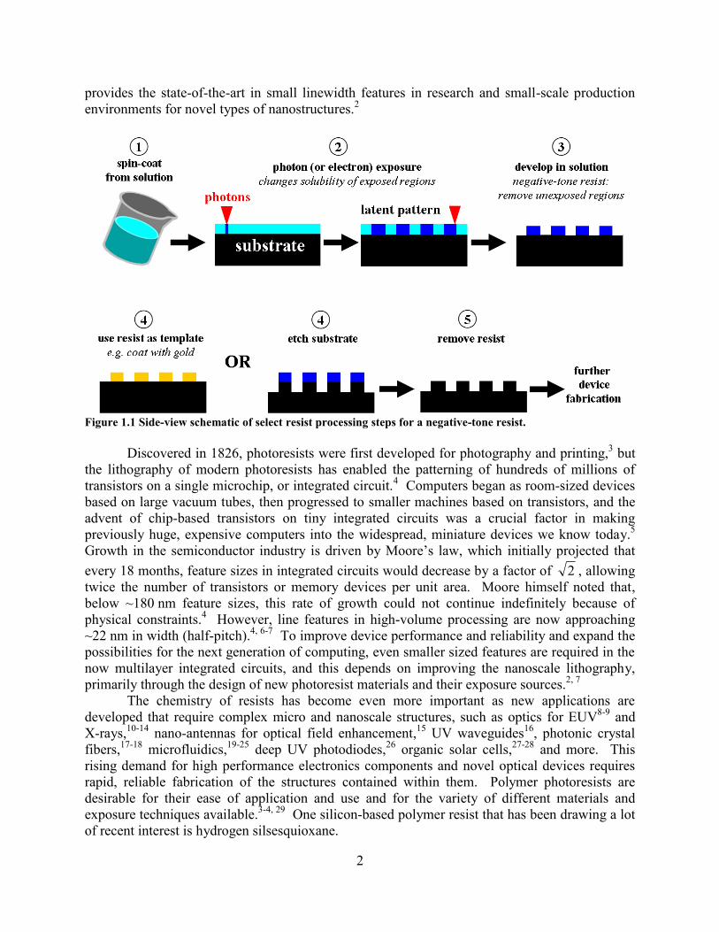
2
provides the state-of-the-art in small linewidth features in research and small-scale production
environments for novel types of nanostructures.2
Figure 1.1 Side-view schematic of select resist processing steps for a negative-tone resist.
Discovered in 1826, photoresists were first developed for photography and printing,3 but
the lithography of modern photoresists has enabled the patterning of hundreds of millions of
transistors on a single microchip, or integrated circuit.4 Computers began as room-sized devices
based on large vacuum tubes, then progressed to smaller machines based on transistors, and the
advent of chip-based transistors on tiny integrated circuits was a crucial factor in making
previously huge, expensive computers into the widespread, miniature devices we know today.5
Growth in the semiconductor industry is driven by Moore’s law, which initially projected that
every 18 months, feature sizes in integrated circuits would decrease by a factor of 2 , allowing
twice the number of transistors or memory devices per unit area. Moore himself noted that,
below ~180 nm feature sizes, this rate of growth could not continue indefinitely because of
physical constraints.4 However, line features in high-volume processing are now approaching
~22 nm in width (half-pitch).4, 6-7
To improve device performance and reliability and expand the
possibilities for the next generation of computing, even smaller sized features are required in the
now multilayer integrated circuits, and this depends on improving the nanoscale lithography,
primarily through the design of new photoresist materials and their exposure sources.2, 7
The chemistry of resists has become even more important as new applications are
developed that require complex micro and nanoscale structures, such as optics for EUV8-9
and
Xrays,10-14
nano-antennas for optical field enhancement,15
UV waveguides16
, photonic crystal
fibers,17-18
microfluidics,19-25
deep UV photodiodes,26
organic solar cells,27-28
and more. This
rising demand for high performance electronics components and novel optical devices requires
rapid, reliable fabrication of the structures contained within them. Polymer photoresists are
desirable for their ease of application and use and for the variety of different materials and
exposure techniques available.3-4, 29
One silicon-based polymer resist that has been drawing a lot
of recent interest is hydrogen silsesquioxane.

3
1.2 Hydrogen silsesquioxane (HSQ) resists
Hydrogen silsesquioxane (HSQ) is a cage-like molecule with the formula H8Si8O12 (often
written HSiO3/2), a member of a class of compounds known collectively as polyhedral
oligomeric silsesquioxanes (POSS),30
shown in Figure 1.2(a). Also known as “spin-on glass”, it
was developed as an interlayer dielectric (ILD) film for multilevel integrated circuits,31-33
where
extremely thin HSQ films are applied from a volatile solution via spin coating, then cross-linked
to an insoluble, glass-like SiO2 network structure via heating,34-36
as shown schematically in
Figure 1.2(b). In 1998 it was discovered that HSQ is also a sensitive electron beam (e-beam)
resist,37
capable of producing nanoscale cross-linked, glass-like features.38
Since then, the
sensitivity of HSQ to a variety of exposure techniques has been demonstrated, including proton
beam,39
helium beam (He+),
40 EUV, and Xray exposure.
41-43
Figure 1.2 Schematic of HSQ (a) cage (monomer) and (b) possible partial network structure (oligomer)
formed by cross-linking two monomer cages. In solution, the molecular structure is actually comprised of
oligomers of various sizes.2
HSQ is a promising negative-tone resist for sub20 nm electron beam (ebeam) and
photolithography because of its small molecular size, low dielectric constant and mechanical
stability,2, 37
but a better understanding of the cross-linking chemistry is necessary to utilize HSQ
and HSQ derivatives for commercial nanolithography applications. In research environments,
ebeam lithography of HSQ is being used to produce high aspect-ratio, nanoscale features as
small as 4.5 nm,1 which are used for optical devices such as EUV diffraction gratings,
8-9 Xray
zone plates,10-14
and nano-antennas,15
as well as high-density line patterns for the next generation
of integrated circuits and computer memory.44-45
However, it is often necessary to vary the
exposure dose and developer conditions in unpredictable ways to achieve precisely the desired
feature size and contrast,2, 46-47
and irreproducibility is caused by delay effects48-49
and area
dependent sensitivity.8, 50-51
Therefore, much work has recently been done to determine the
optimum parameters for achieving the smallest features in e-beam lithography of HSQ,1, 46, 51-52
but unanswered questions remain.2
While e-beam lithography is an important patterning modality for HSQ, commercial
integrated circuit manufacturing typically requires high-throughput optical lithography. Toward
this goal, EUV interference lithography has been used in HSQ for dense line patterns down to
20 nm half-pitch,53
and X-ray exposure behind a mask can create isolated features in HSQ down

4
to 11 nm wide in a 50 nm thick film.54-55
Thus HSQ line widths surpass the resolution possible
with conventional chemically amplified polymer photoresists,44
but with insufficient sensitivity
and reproducibility for high-throughput commercial applications. Therefore, new and improved
HSQ derived and HSQ-like materials are currently being developed,56
but progress could be
hastened by understanding the fundamental chemistry that causes the current challenges with
HSQ. There have been a variety of studies that aim to determine the thermally induced reaction
mechanism of HSQ, mostly with FTIR spectroscopy,34, 57-58
but more study is needed to fully
characterize the photo-induced cross-linking mechanism applicable to the micro and nano-
patterning of HSQ. A better understanding of the solid-state, nanoscale cross-linking chemistry
is necessary to unlock the full potential of this material and its derivatives for the next generation
of commercial applications, and this is where microspectroscopy techniques such as broadband
coherent anti-stokes Raman scattering (CARS) and scanning transmission X-ray microscopy
(STXM) can play a key role.
1.3 Multiphoton absorption polymerization
Multiphoton absorption polymerization (MAP) is another relatively new technique for
producing fine patterns in polymer photoresists. Feature resolution in traditional photo-
lithography is intrinsically diffraction limited (~λ/2), but relatively inexpensive pulsed visible
and near IR lasers can be used to produce sub-diffraction limited sized features in materials that
otherwise absorb only in the UV or EUV, as the probability for simultaneous multiphoton
absorption is highest only within the very center of the focused beam profile. As with other non-
linear optical processes, such as two-photon fluorescence or CARS, the probability for inducing
the cross-linking reaction is greatly increased when the power density, or number of photons per
unit time, is very high, as occurs during the very short pulses of ultrafast lasers. The power
density during the “on” time of an ultrafast pulse is referred to as the peak power. The resolution
enhancement in multiphoton processes is greater when more photons are required to initiate the
process of interest (cross-linking, bond-breaking, ablation, signal generation, etc.), because the
necessary peak power can only be found at smaller and smaller regions within the focal
volume.59
Through other creative manipulations of multiple laser beams, features down to λ/20
resolution have been produced with 800 nm exposure (i.e. 40 nm features).60
Another advantage of MAP is the capability to produce complex or layered three-
dimensional structures in thicker films (>1 μm), because the nonlinear photoactivation process
does not occur all along the beam path, but only in the region of highest power density within the
focus. Thus, the beam can be scanned not only laterally but also throughout the depth of the
sample to initiate cross-linking in very precise domains in x, y and z. Fascinating 3D structures
have been produced by MAP in photoresists that would not be possible with single-photon
excitation methods, from micromachines61-62
to photonic crystal fiber arrays17
to novel
microfluidics63-64
and other layered microstructures65
. As the resolution of MAP is increased, it
is conceivable that functional 3D nanostructures will also be fabricated in this way. In the
experiments presented here, near-IR MAP of HSQ is demonstrated for the first time, along with
an analysis of the cross-linking kinetics and the non-linear power dependence of the process
under various conditions, studied in real time with broadband coherent anti-Stokes Raman
scattering (CARS) spectroscopy.
5
1.4 Microspectroscopy of photoresists
High resolution, chemically selective imaging is a sought after tool in many fields, from
biology to materials science, including mapping of latent (undeveloped) patterns in polymer
photoresists for design and quality control purposes. In most studies of HSQ lithography,
exposure is followed by development in solution and subsequent imaging with scanning electron
microscopy (SEM), scanning tunneling microscopy (STM) or atomic force microscopy (AFM).
These techniques can provide down to atomic spatial resolution, but little to no chemical
information, and are only surface sensitive. For understanding the exposure-induced cross-
linking process, one drawback to analyzing resists after development is that the chemical effects
of exposure are coupled with the development chemistry, and the features produced are
extremely sensitive to small changes in the development process.47, 51, 66-67
In contrast, FTIR
spectroscopy has been utilized to study chemical changes in undeveloped HSQ due to thermal
curing or ebeam exposure,34, 58
and FTIR microspectroscopy is used to image the spatial
distribution of the cross-linking reaction and functional groups in latent ebeam patterns,68
but is
limited to ~10 μm spatial resolution at best. By comparison, broadband coherent anti-Stokes
Raman scattering (CARS) microscopy and scanning transmission X-ray microscopy (STXM)
provide higher spatial resolution (~400 nm and 30 nm, respectively), fast acquisition time (from
tens of milliseconds to seconds) and very high chemical selectivity for microspectroscopy and
imaging of latent resist patterns.
1.4.1 Coherent anti-Stokes Raman scattering microscopy
Raman scattering spectroscopy and microscopy is widely used in biological and physical
sciences for sample identification and imaging, as it provides a “fingerprint” spectrum of the
molecules in a sample based only on their intrinsic vibrational modes, without the need for any
labeling or staining. Despite the low cross-section for Raman scattering of ~10-25
cm2, it offers a
powerful way to peer into many samples and organisms, and so many variations of Raman
scattering have emerged over the years. One method for enhancing the signal strength, and
hence the sensitivity, of Raman scattering is a nonlinear process called coherent anti-Stokes
Raman scattering (CARS). Since its discovery in 1964,69
CARS has been used to study a wide
variety of samples and systems, from measurement of combustion temperatures70
to tissues in
vivo.71-72
The first CARS microscope was demonstrated in 1982,73
and in 1999 a focus on
biological imaging using CARS microscopy began a new wave of discovery and innovation in
CARS microscope development.74
The first CARS microscopes, and most in use today, utilize narrowband lasers to probe
one single Raman-active vibrational mode at a time. Very sensitive and rapid images have been
measured with narrowband CARS microscopy, including images of latent patterns in polymer
photoresists.75
However, a broader vibrational spectrum is needed to simultaneously quantify
multiple materials within each region of the resist, especially for chemicals with very similar
spectral features, such as cage versus cross-linked HSQ. To this end, it is possible to incorporate
a broadband laser to acquire multiplex or broadband CARS spectra, explained in detail in section
2.1. The fast spectral acquisition of broadband CARS allows monitoring of changes in the
spectrum as the rapid HSQ cross-linking reaction occurs. While the kinetics of solution phase
reactions can be studied at a slower rate by dilution, such dilution is not possible for most solid-

6
state samples, such as polymer photoresist thin films, without totally altering the composition
and chemistry of the films. Previous FTIR measurements of thermally cross-linked HSQ films
were limited to 1-2 minute time resolution by sample heating and cooling times, but it was
shown that most of the cross-linking occurs within the first minutes of heating.58
On the other
hand, real-time FTIR measurements of solid state kinetics in other, very thick (~25 μm to 5 mm)
photoreactive polymers have been reported, which offer higher time resolution, on the order of
~20 ms,76-78
but this technique has not been applied to the study of HSQ. Similar in concept to
real-time FTIR, the sub-second time resolution of the broadband CARS method employed here
provides detail about the early stages of the HSQ cross-linking in thin films as the process is
monitored in situ.79
Furthermore, the same pulsed near IR light source used for the CARS
spectroscopy is also used here to induce multiphoton HSQ cross-linking. Due to the non-
linearity of the process, control of the temporal and spectral profile of the laser pulses allows the
cross-linking rate to be finely controlled, even to a level that it initiates (essentially) no cross-
linking, while maintaining a strong CARS signal intensity.
1.4.2 Scanning transmission X-ray microscopy
While CARS can provide a great amount of chemical information on a relatively short
time scale, the spatial resolution is limited to ~300-400 nm. To understand the behavior of
photoresists for nanostructure fabrication, chemical information at much higher spatial resolution
is required, a need fulfilled by scanning transmission X-ray microscopy (STXM). In STXM,
Xrays are focused on a thin sample and the transmitted flux is measured as the sample is raster
scanned perpendicular to the X-ray beam to create a pixel-by-pixel image. In routine state-of-
the-art X-ray microscopy, the typical spatial resolution is ~30 nm, achieved by focusing the X-
rays with a diffraction based Fresnel zone-plate with an outermost zone radius of 25 nm, as
detailed in section 2.4. Zone plates with 12 and 15 nm outer zone radius have recently been
fabricated for the next generation of improved resolution STXM instruments,10-12
and
interestingly, e-beam lithography of HSQ resists is used to fabricate these very zone plates.
When an X-ray of sufficient energy interacts with an atom, it can be absorbed by
promoting a photoelectron from one of the inner core shells. The near edge X-ray absorption
fine structure (NEXAFS) spectrum, explained in section 2.3, reveals the element-specific local
electronic structure of a material. The high resolution STXM at beamline 5.3.2 of the Advanced
Light Source (ALS) at Lawrence Berkeley National Lab was specifically designed for the study
of polymeric materials through their carbon, nitrogen and oxygen 1s absorption edge NEXAFS
spectra (core binding energies of approximately 280 eV, 410 eV and 543 eV, respectively), and
several different positive and negative-tone photoresists have previously been imaged and
studied at this STXM.50, 80-81
An additional, undulator-based STXM at beamline 11.0.2 of the
ALS extends the accessible energy range to 130 eV - 2000 eV, which encompasses the ~1850 eV
K-edge absorption of silicon, also useful for the study of HSQ. Recently, the first STXM studies
of HSQ thin films were performed on latent e-beam patterns at beamlines 5.3.2 and 11.0.2,
revealing differences in the NEXAFS spectrum of the cage versus cross-linked HSQ, and a
significant, unexpected spatial spread of the reaction beyond the e-beam exposure boundaries.50
Reaction spread is also observed in this work after Xray exposure, which is explored in detail in
section 5.6.

7
Due to the high photon energies used, X-ray microscopy can induce sample damage. The
STXM interface allows the user to balance signal levels with photodamage by minimizing the
total radiation dose delivered during imaging and spectroscopy. HSQ is known to be sensitive to
X-ray exposure, so significant optimization is required to acquire HSQ images and spectra in the
STXM without inducing significant sample cross-linking. However, it is likewise possible to
increase the X-ray flux through the sample in order to induce bond scission or cross-linking of
polymers, a concept recently explored for direct-write patterning of positive tone polymer
photoresists such as PMMA (polymethylmethacrylate) and PAN (polyacrylonitrile).81-82
As
reported in this work, this Xray induced cross-linking can also be used to directly write patterns
in the HSQ films.83
The beam diameter (FWHM) at the focus is ≤50 nm and the position of the
sample in the beam can be controlled with <10 nm of jitter, so fine patterns can be written
directly by the X-ray beam by scanning the sample through the beam in a pre-defined pattern
with a sufficient photon flux and per-point exposure time. Photolithography of HSQ is a sought-
after tool for high-throughput resist processing, so a number of studies have investigated the
limits and characteristics of EUV and X-ray lithography of HSQ, where blanket exposures
through a mask are typically used.41-43, 53-55, 84-85
Direct-write patterning with the STXM is
slower than such blanket exposures, to be sure, but it enables characterization of the films
immediately after patterning, minimizing the post-patterning delay (during which sample
changes may occur)2, 48-49
and eliminating the development step prior to analysis of the
photochemistry. Thus, STXM is used to investigate in detail the X-ray induced cross-linking
chemistry and reaction rate and to define the spatial extent of the reaction spread. These results
provide insight into the photolithography mechanism, and hopefully provide some guidance on
how new silicon-based photoresist materials might be altered for faster, more reliable
nanolithography.
1.5 Outline: Optimizing microspectroscopy techniques to study HSQ
chemistry
A detailed review of the theory and design of the novel, single-beam broadband CARS
method is given in Chapter 2, with examples of (damage-free) polymer blend imaging to
demonstrate the temporal and spatial resolution of the technique. This is followed by a brief
overview of the theory of NEXAFS spectroscopy, the design of the (well-established) STXM
microscope at beamline 5.3.2, and the optimization of the STXM framework for direct-write
Xray patterning of HSQ thin films. The discovery of near IR multiphoton HSQ cross-linking is
presented in Chapter 3, followed by an analysis of the CARS and spontaneous Raman spectral
intensities and lineshapes of HSQ thin films. In Chapter 4 broadband CARS is utilized to reveal
the power-dependent cross-linking rate, and possible HSQ cross-linking mechanisms are
discussed in detail, especially as they pertain to the multiphoton-induced cross-linking. In
Chapter 5, cross-linked patterns are produced in HSQ thin films with the focused Xray beam of
the STXM. NEXAFS spectra and STXM images of the latent patterns, along with spectra of
related POSS compounds, reveal details about X-ray cross-linking mechanism and reaction rates,
analogous and complementary to the CARS results. Furthermore, a common reproducibility
effect in HSQ is observed and explained by measuring the spatial extent of the spread in X-ray
patterned features with 30 nm resolution. Several of the X-ray patterned films are developed and
imaged with SEM to compare the feature characteristics before and after development.

8
Connections are drawn between the CARS and STXM HSQ results in Chapter 6 and discussed in
the context of previously reported phenomena, along with preliminary results regarding cross-
linking inhibitors and ideas for future research directions in studying the photochemistry of HSQ
and improving its photolithography characteristics for current and new applications.
9
2 Experimental techniques: theory and design
2.1 Coherent anti-Stokes Raman scattering (CARS)
When light is scattered by a molecule, elastic (Rayleigh) scattering is the most probable,
whereby the scattered light has the same frequency as the incident light. Following classical
electrodynamics, the scattering is produced by the oscillating polarization (dipole) of the
molecule induced by the incident electric field of the light:
tEtPRayleigh 0cos)(
, (2.1)
where P
is the induced (transient) dipole oscillating with frequency ω0, α is the polarizability
(tensor) of the molecule and E
is the amplitude of the incident electric field, also of frequency
ω0. In rare instances – about 1 in 107 scattering events – inelastic Raman scattering occurs,
shifting the incoming frequency by the energy of the vibrational modes of the molecule:
])cos()[cos()( 00
0 ttQ
QEtP ii
i
iRaman
, (2.2)
where ωi is the ith
vibrational frequency of the molecule with an amplitude of Qi0, and
Q
is the
(first order) change in the polarizability with the vibrational motion along the molecular
vibrational (normal) coordinate Qi, which must be non-zero for Raman scattering to occur. Thus,
depending on the initial vibrational state of the molecule, the frequency of the Raman scattered
light can be lower (Stokes, ω0- ωi) or higher (anti-Stokes, ω0+ωi) than the incident light, as
shown in Figure 2.1(a).
While infrared absorption only occurs when there is a change in the permanent dipole
moment along the vibrational coordinate, Raman scattering requires that the polarizability
changes with the vibrational motion. Therefore, some vibrational modes not accessible in IR
spectroscopy can be observed with Raman, and vice versa. (Specifically, in molecules with a
center of symmetry, vibrational modes can be either Raman or IR active, but not both.) When
the light has a wavelength far longer (lower energy) than any electronic transitions in the atom,
then the polarizability is independent of wavelength (although the scattered light intensity does
vary as 4
0 ). Therefore, unlike IR absorption, Raman spectra can be obtained from a
monochromatic source of almost any color in the visible to near IR portion of the
electromagnetic spectrum, avoiding direct electronic excitation or IR absorption. Since the
incident light is not in the IR, water is transparent and thus hydrated samples do not pose a
problem as they do in IR spectroscopy. Also, if the polarization of the incoming light is not
oriented parallel to one of the principal axes of the polarizabilty of the molecule, the scattered
light will be depolarized; that is, it will have some portion polarized perpendicular to the incident
field, E
. This will be discussed in more detail when depolarization Raman spectra of HSQ are
presented in section 3.4.
10
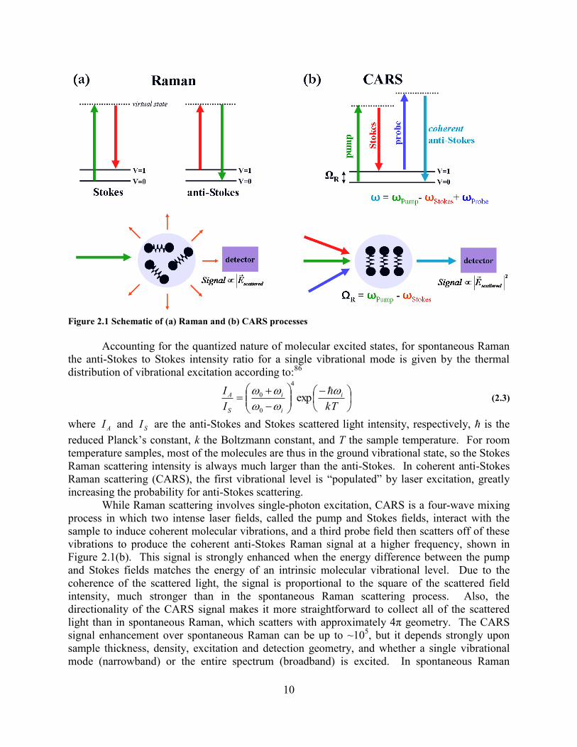
Figure 2.1 Schematic of (a) Raman and (b) CARS processes
Accounting for the quantized nature of molecular excited states, for spontaneous Raman
the anti-Stokes to Stokes intensity ratio for a single vibrational mode is given by the thermal
distribution of vibrational excitation according to:86
kTI
I i
i
i
S
A
exp
4
0
0 (2.3)
where AI and SI are the anti-Stokes and Stokes scattered light intensity, respectively, ħ is the
reduced Planck’s constant, k the Boltzmann constant, and T the sample temperature. For room
temperature samples, most of the molecules are thus in the ground vibrational state, so the Stokes
Raman scattering intensity is always much larger than the anti-Stokes. In coherent anti-Stokes
Raman scattering (CARS), the first vibrational level is “populated” by laser excitation, greatly
increasing the probability for anti-Stokes scattering.
While Raman scattering involves single-photon excitation, CARS is a four-wave mixing
process in which two intense laser fields, called the pump and Stokes fields, interact with the
sample to induce coherent molecular vibrations, and a third probe field then scatters off of these
vibrations to produce the coherent anti-Stokes Raman signal at a higher frequency, shown in
Figure 2.1(b). This signal is strongly enhanced when the energy difference between the pump
and Stokes fields matches the energy of an intrinsic molecular vibrational level. Due to the
coherence of the scattered light, the signal is proportional to the square of the scattered field
intensity, much stronger than in the spontaneous Raman scattering process. Also, the
directionality of the CARS signal makes it more straightforward to collect all of the scattered
light than in spontaneous Raman, which scatters with approximately 4π geometry. The CARS
signal enhancement over spontaneous Raman can be up to ~105, but it depends strongly upon
sample thickness, density, excitation and detection geometry, and whether a single vibrational
mode (narrowband) or the entire spectrum (broadband) is excited. In spontaneous Raman
11
scattering, the Stokes signal is typically used for microscopy and sample identification because
the anti-Stokes signal is significantly weaker. One big advantage of detecting the anti-Stokes
term instead is the absence of overlap with the fluorescence, especially in samples with strong
fluorescence under laser illumination.
The induced polarization due to higher order photon interactions (to third order) is:
3)3(2)2()1( EEEP
, (2.4)
where )(n is the nth
order susceptibility of the molecule, which is a tensor of rank n +1, and E
is
again the electric field of the incident light.87
Thus, )1( , the polarizability of the molecule,
which accounts for Rayleigh and spontaneous Raman scattering, )2( is responsible for second-
order processes such as second harmonic generation, and )3( is a fourth-rank tensor called the
third-order nonlinear susceptibility, responsible for the coherent anti-Stokes Raman scattering
process. The total )3( contains contributions from many other possible frequency combinations
of the incident fields which do not correspond to CARS, such as third harmonic generation and
other instantaneous electronic four-wave mixing processes. Since we are interested only in
vibrational resonances leading to CARS signal, all the other third-order processes besides CARS
will be defined as nonresonant (NR), giving:
)3()3()3( )()( NRR , (2.5)
where )()3( R is the resonant CARS part of the third-order nonlinear susceptibility, and )3(
NR
is the nonresonant part, which are given by:
RR
R
R
RRi
a
)3(
(2.6)
and:
NRNR
)3(
(2.7)
where αR and αNR are the amplitude coefficients for the resonant and NR susceptibilities,
respectively, aR, ΩR and ΓR are the intensity, energy and line width of vibrational mode R,
respectively, and Pr , where ωPr is the frequency of the probe field.88-89
Thus,
)3(
NR is purely a real quantity, but )()3(R contains real and imaginary parts,
corresponding to the phase shift that occurs during forced, damped vibrations, as experienced
here by the electric-field induced oscillating dipole.90
Thus, vibrational excitations have
Lorentzian natural lineshapes, and the imaginary part of this lineshape is what is detected in
spontaneous Raman spectroscopy.91
The signal detected at frequency ω is enhanced when the
difference between the pump and Stokes fields is in resonance with a vibrational frequency of
the molecule, as shown in Figure 2.1(b). That is, the signal is most enhanced when:
RPS (2.8)
where ωP and ωS are the frequency of the pump and Stokes fields, respectively. Thus, when
sP is tuned to a vibrational resonance, the total signal at frequency ω is a combination of
both resonant anti-Stokes Raman scattering and NR four-wave mixing signals. The implications
of the complex nature of )3(
R on the CARS signal intensity and lineshape are further
explored in section 2.2.1.

12
Typically, narrowband CARS utilizes one picosecond laser to supply the pump and probe
beams at the same frequency and a second picosecond laser for the energy-shifted Stokes beam
[Figure 2.1(b) and Figure 2.2(a)]. Single vibrational resonances can be probed one at a time by
tuning the difference between the pump/probe and Stokes beams to match these vibrational
frequencies. However, since the vibrational fingerprint region extends from about 800 to
1800 cm-1
, it is desirable to simultaneously acquire this full vibrational spectrum at each spatial
location in a sample. To accomplish this, a broadband pump beam can be used to excite multiple
vibrational modes simultaneously, while a narrow probe beam provides higher spectral
resolution in the CARS spectrum [Figure 2.2(b)], and this is known as multiplex or broadband
CARS, depending on the frequency range of the technique used. Multiple definitions have been
proposed, but typically multiplex CARS refers to techniques with <1000 cm-1
of bandwidth,
while broadband CARS applies when 10003000 cm-1
of bandwidth are accessible. There are,
however, tradeoffs necessary to gain this spectral width. With narrowband CARS the signal
sensitivity and signal acquisition rate can be much higher, but with broadband CARS the full
Raman-equivalent spectrum is provided in a single pulse, and in microscopy the spatial locations
of multiple species can therefore be obtained in a single image scan. Also, higher laser power is
necessary to populate and measure all the vibrational modes for broadband CARS versus a single
mode in narrowband CARS, increasing the risk of sample damage. For broadband CARS, the
nonresonant signal due to )3(
NR can even exceed the resonant CARS signal, as there are
many different combinations of the three fields that contribute to the NR signal at each
frequency. As such, significant signal manipulation is required to retrieve the smaller resonant
signal and Raman-equivalent spectrum.
Figure 2.2 Schematic of (a) narrowband vs (b) broadband CARS processes.
13
2.2 Single-beam, broadband CARS microscopy
A variety of novel coherent anti-Stokes Raman scattering (CARS) methods have been
developed in recent years that utilize ultrafast lasers, sometimes with a chirped or fiber-
broadened spectrum, to obtain broadband vibrational information from molecules.92-102
For a
narrow bandwidth probe, these techniques typically employ a second, narrowband laser or use a
split beam in two paths to generate the broadband and narrowband components separately. An
important advantage of these broadband methods for microscopy is that full chemical
composition analysis is possible in a single microscope scan, rather than the multiple scans that
are necessary with narrowband CARS microscopy. However, due to the high peak-power of the
ultrafast pulses, purely electronic four-wave mixing processes within the sample lead to a much
larger NR background across the entire spectrum [not shown in Figure 2.2(b)]. This large NR
signal and its corresponding shot noise have been the primary challenge for implementing
sensitive broadband CARS spectroscopy. Since this NR signal results from the interaction of the
laser field with the sample of interest, creative manipulations are necessary for suppression or
elimination of this NR background so that the much smaller intensity resonant spectrum can be
obtained.
An important breakthrough came when phase and polarization pulse shaping techniques
were employed to obtain multiplex CARS spectra with a single laser beam from an ultrafast
laser, eliminating complications associated with tuning, timing and alignment between two
separate beams.103
The whole array of pump and Stokes frequencies were provided
simultaneously by the broadband pulse, and the resulting coherent molecular vibrations were
probed by a narrow spectral part of the total bandwidth within the same laser pulse. The narrow
probe part of the beam was differentiated only by shifting the phase and polarization of that
narrow spectral region of the laser pulse, but not separated spatially from the broadband part of
the beam. Furthermore, single-beam pulse shaping methods were developed to significantly
reduce or eliminate the NR background,104
and fingerprint-region CARS spectra with up to
700 cm-1
of bandwidth were previously obtained.105
A novel variation of this pulse shaping and signal acquisition scheme developed
previously in our laboratory improves the sensitivity to allow spectra and spectral images to be
obtained in an even shorter acquisition time with up to 1000 cm-1
of bandwidth per spectrum.88
The essential feature of this method is the use of a single, femtosecond (fs) pulsed laser, which
simultaneously provides all three photons necessary to produce the CARS signal, followed by
pulse shaping and spectral interferometry of the signals within the single beam. Rather than
eliminating the NR signal prior to detection, the NR signal is utilized as a local oscillator for
homodyne amplification of the resonant signal. With this fast, single-beam, broadband CARS
spectroscopy, spectral images are acquired in the vibrational fingerprint regime,89
and the time-
dependent spectra during photochemical conversion are measured to determine solid-state cross-
linking kinetics of HSQ.79
2.2.1 Double Quadrature Spectral Interferometry (DQSI) CARS
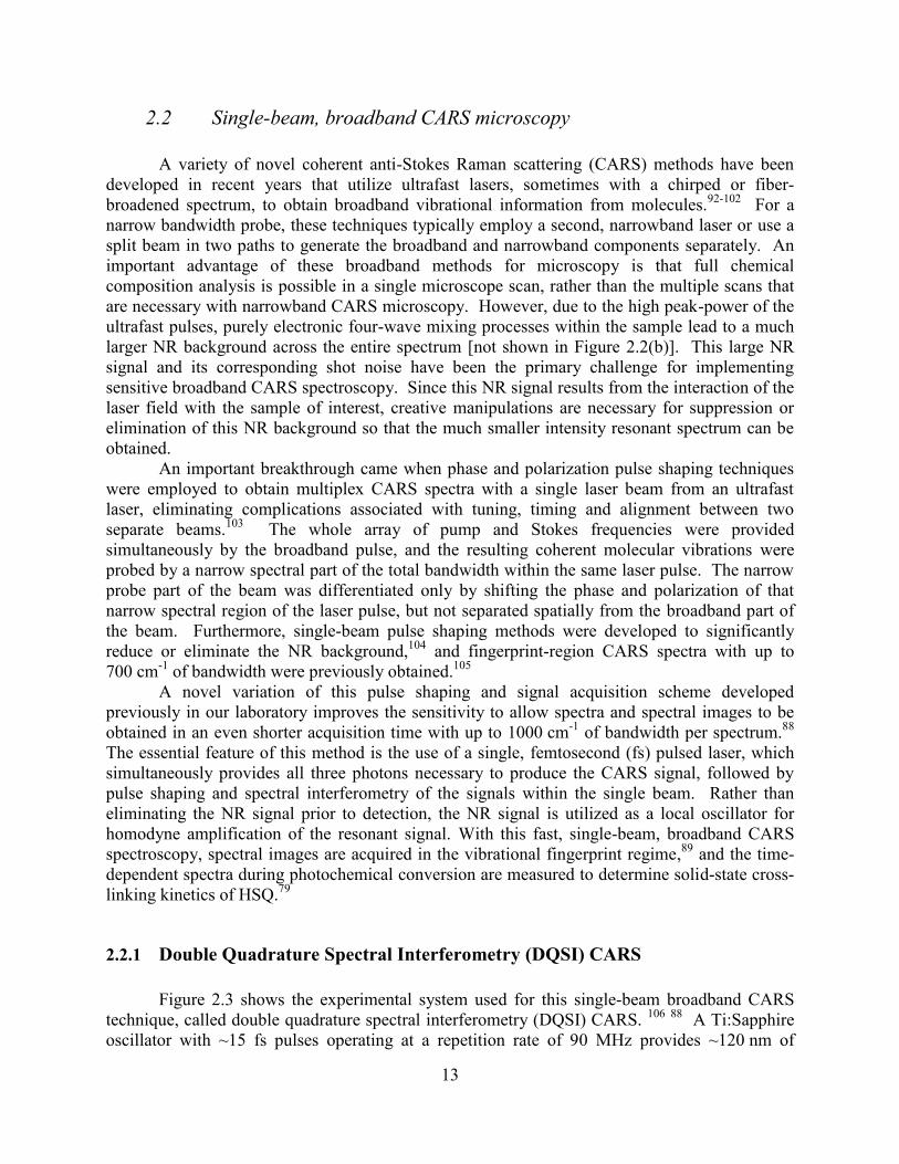
Figure 2.3 shows the experimental system used for this single-beam broadband CARS
technique, called double quadrature spectral interferometry (DQSI) CARS. 106
88
A Ti:Sapphire
oscillator with ~15 fs pulses operating at a repetition rate of 90 MHz provides ~120 nm of
14
bandwidth centered at a wavelength of ~800 nm (MTS, KM Labs). After the laser beam is
expanded, it passes through an all-reflective 4f geometry pulse shaper, shown in Figure 2.4. It is
dispersed horizontally (parallel to laser table) by an 800 grooves/mm diffraction grating,
collimated by a spherical mirror, passed through a dual-mask spatial light modulator
(SLM 640D, CRi), and then refocused and re-compressed by an additional spherical mirror and
grating. The SLM consists of two banks of 640 liquid crystal pixels whose birefringence is
controlled by changing the applied voltage to the individual pixels, explained in detail in the
following section.
Figure 2.3 DQSI CARS experimental setup.

15
Figure 2.4 (a) Schematic top view of pulse shaper, with SLM at center. (b) Top view photograph of pulse
shaper. Note that the dispersed beam passes over the top of the small entrance and exit mirrors.
The pulse shaper serves two purposes: producing a narrowband probe field within the
broadband beam, and compressing the spectral phase (chirp) introduced in the ultrafast pulse
along the beam path. As the dispersed laser beam passes through the SLM, the probe field is
differentiated from the remainder of the spectrum by shifting the phase and polarization of just a
very narrow portion of the spectrum, which is described in detail below. Furthermore, with such
a broad bandwidth spectrum, any difference in optical path length between the different
frequencies introduces significant spectral phase, corresponding to temporal dispersion (chirp)
which stretches the pulse duration and lowers the peak power. The SLM can be used to
compensate for this spectral phase, resulting in the shortest possible pulses and highest peak
power at the sample position in the microscope focus, a critical factor in achieving high CARS
signal intensity and multiphoton HSQ cross-linking. The pulse shaping and chirp compression
techniques are explained in the following section (2.2.2).
After phase and polarization pulse shaping, the beam is again collimated and the light is
focused through a 1.2 numerical aperture (NA), near IR optimized, water immersion microscope
objective (60× UPlanApo, Olympus) into a condensed phase sample on an XY piezoelectric
translation stage (Physik Instrumente). After interaction with the sample, the light is collected
through a 0.85 NA air objective or 1.0 NA water immersion objective (60x PlanFluor, Olympus)
and the laser frequencies are filtered out with a sharp-edge short-wave pass filter (740 AESP,
Omega Optical). The polarization of the light is rotated by 45° by an achromatic half-wave plate
(Fresnel rhomb, CVI), and the signal is split spatially into two separate directions using a
Rochon prism (CVI). Both signal traces are focused into a spectrometer (SP-2300i, PI-Acton)
and the resulting spectra are imaged onto a two-dimensional CCD detector (DV-401-FI, Andor).
The resonant (CARS) and NR parts of the signal can be considered independently, where
PR is the resonant transient induced polarization, given by:
0
Pr
)3( dAEP RR (2.9)
and PNR is the NR transient induced polarization:
16
0
Pr
)3( dAEP NRNR . (2.10)
EPr(ω-Ω) is the narrowband probe, and the amplitude of the excitation is given by:
0
* dEEA SP (2.11)
where EP and ES are the pump and Stokes fields, respectively. Thus, the resonant and NR
contributions to the total signal, S(ω) are:
RRNRNRRRNRR PPPPPPPPS *2*2 (2.12)
As noted in the previous section, the NR contribution is entirely real, but the resonant part of the
signal contains both real and imaginary parts. This is evident by approximating EPr as a delta
function and inserting the equations for the third order susceptibility (equations 2.6 and 2.7) into
equations 2.9 and 2.10, giving:
Pr
Pr
i
RR eLAP (2.13)
0d
AP NRNR (2.14)
where L(ω) is now the Lorentzian lineshape function for the resonant CARS:
R RR
R
i
aL
Pr
. (2.15)
The purely resonant part of the total signal, RR PP* , is the smallest term while the NR part,
[PNR(ω)]2, is the largest term. The cross term in equation 2.12, PNR(ω)[ *
RP (ω) + PR(ω)], is linear
in the NR contribution, but also contains the real and imaginary parts of the resonant
contribution. The technique used here detects this larger cross-term, in which the NR signal
effectively amplifies the resonant signal, so-called homodyne amplification.
The NR background and resonant CARS signals are coherent and phase locked with each
other. While the resonant signal depends on the phase of the probe part of the pulse, most of the
NR signal is produced by the broadband part of the pulse, which has a different phase. Thus, it is
possible to implement interferometry between the resonant and NR parts of the signal by
controlling the phase difference between them. Inducing different phase shifts in the probe part
of the pulse with respect to the broadband part results in different spectral interference between
the resonant and NR signals that are acquired simultaneously. Also, in order to directly obtain
the resonant CARS spectrum using broadband pulses, the NR background must be eliminated.
By altering the polarization of the probe part of the pulse, the signal can be separated into two
slightly different spectra (i and j), as shown in Figure 2.5(a) and (b). The resonant contributions
to these two spectra are equal in magnitude but opposite in sign:
R
i
R PP2
1 and R
j
R PP2
1 (2.16)
while the signals at both polarizations contain the same NR background:
NR
j
NR
i
NR PPP2
1 (2.17)
resulting in an equal but opposite interference between the resonant and NR signal in the two
spectra (i and j) at the vibrational resonances, shown in Figure 2.5(b) for toluene. Note that these
two spectra are acquired simultaneously on the CCD. Thus the total signal in each trace is
obtained by plugging 2.16 into equation 2.12:

17
2
i
NR
i
R
i PPS and 2
j
NR
i
R
j PPS (2.18)
Expanding 2.18 and subtracting one spectrum from the other results in the difference signal:
PrPrPr sinImcosRe2 LLAPSS NRR
ji . (2.19)
Thus, with ϕPr=90 the real part becomes zero and only the imaginary part of the lineshape is
detected, corresponding directly to the spontaneous Raman scattering line shape, as shown in
Figure 2.5(c). Considering that the resonant signal is much smaller than the non-resonant, the
sum of the signals, Si+S
j, will be mostly non-resonant signal. Thus, the normalized signal
intensity, SN, in units of counts , is equivalent to non-amplified field amplitude of the resonant
CARS signal only, given by:
LA
SS
SSS Rji
ji
N Im2 Pr
(2.20)
Because the two signal traces are detected 90° out of phase (in quadrature), the method is called
double quadrature spectral interferometry (DQSI) CARS.88
Figure 2.5 DQSI CARS detection scheme,
107-108 showing (a) polarization of incident fields and detected
signals, (b) total signal from toluene for each spectrum and (c) difference of two signals.
Note that the NR signal from the sample itself serves as the local oscillator here, which
amplifies the resonant signal significantly, providing a sensitivity improvement over previous
CARS spectroscopy techniques in which the NR signal is suppressed prior to detection. Since
the local oscillator comes from the sample itself, this is called homodyne amplification.
Heterodyne amplification of the CARS signal has been previously demonstrated, where the
resonant and NR spectra were acquired separately from different samples, followed by
interfermometry between the two signals using an interferometer.100, 109
The key improvement
here is that there is no need for separate beams prior to the sample or an interferometer, since the
18
interferometry takes place within the single beam. Thus the key advantages of this technique
(versus other broadband CARS techniques) are the single beam configuration, signal
enhancement by homodyne amplification with the NR signal, and the Raman-like line shape.
Furthermore, the normalized signal intensities are linearly proportional to the concentration of
the vibrational modes/molecules being detected, as in spontaneous Raman spectroscopy; this is
not the case in most other CARS microscopy techniques.
Sample damage due to three-photon absorption and subsequent local heating is a limiting
factor in many types of samples. Samples in solution or surrounded by water show increased
resilience to photo-degradation, but fast scan rates make it possible to acquire spectral images of
more readily damaged polymers; an example of this is shown in Figure 2.6.108, 110
A thin-film of
polymethylmethacrylate (PMMA) and polystyrene (PS), which are known to phase separate,111
is
prepared by dissolving 1:1 PMMA/PS in chloroform and spin-casting the solution into a film
approximately 2-5 μm thick (verified with AFM). The sample is placed in the microscope
perpendicular to the laser beam and scanned through the laser focus in the XY direction with the
piezoelectric translation stage. A spectrum is obtained in 10 ms for each pixel in the image. The
spectra for the individual materials are shown in Figure 2.6(a)-(b). The image is 100 pixels ×
100 pixels, containing a total of 10,000 separate spectra. The total image size is 20 µm × 20 µm,
and the total time for data acquisition and transfer is about 3.5 minutes. The spectra for the two
polymers have similar features around both 1000 cm-1
and 800 cm-1
, so chemically selective
imaging requires a full spectrum and analysis of the ratio of the peak intensities for each pixel in
the image. The false-color contrast scale for the image in Figure 2.6(c) is shown, where the
bright red corresponds to 1000 cm-1
/800 cm-1
= 4, the ratio of the spectral peaks in the pure PS
spectrum, and the dark blue is 1000 cm1
/800 cm-1
= 0.5, corresponding to pure PMMA. With
current state-of-the-art spontaneous Raman microscopy systems, it typically takes one second or
more to acquire each of these spectra with the same signal-to-noise ratio, which would result in a
total imaging time of three hours for a scan of similar size and spatial resolution. The spatial
resolution in Figure 2.6 is about 400 nm, which is less than expected theoretically. Due to the
third order nonlinearity of the CARS signal, enhanced spatial resolution of 230 nm is expected
under these conditions, and <300 nm resolution has previously been observed.75, 89
The
degradation of the spatial resolution is most likely the result of slight chromatic aberrations and
misalignment through the focusing objective, which can be significant due to the exceptionally
broad bandwidth of the spectrum.

19
Figure 2.6 DQSI-CARS spectra of (a) PS and (b) PMMA, acquired in 10 ms each. (c) DQSI CARS spectral
image of a self-segregated PMMA/PS blend, acquired in 3.5 minutes.108, 110
Acquiring the full spectrum at each pixel enables not only imaging of multiple
components with similar spectral features, but also ratiometric analysis of the relative amounts of
each component at a particular position. For example, in Figure 2.6(c), regions containing a
blend of PS and PMMA are observed, shown in light blue, green and yellow, depending on the
fraction of PMMA or PS present. This is important for the study of HSQ photoresists because
the cage and network structures, and hence their Raman spectra, are very similar. For imaging
and microspectroscopy, the amount of cage versus cross-linked HSQ at each sample position is
desired, which reveals the relative degree of cross-linking. Spontaneous Raman and CARS
spectra of HSQ thin films are not found in the literature, so they are reported with the
experimental results in section 3.4.
2.2.2 Pulse Shaping and Compression with a Spatial Light Modulator
The heart of the single beam, broadband CARS microscope is the dual mask, liquid
crystal spatial light modulator (SLM), shown in Figure 2.7. This device allows independent
control of the phase and polarization of individual frequency components of the broadband laser
spectrum; with the simple addition of an exit polarizer, this translates to phase and amplitude
control. With 640 pixels spanning the full laser spectrum from 700 to 900 nm, each SLM pixel
controls a spectral range of ~0.3 nm. As the precise control of the SLM is critical to obtain the
CARS spectra and control the peak power at the microscope focus for multiphoton absorption
polymerization, a brief explanation of its operation is given here. Interestingly, the dispersed
laser spectrum is visible in the photographs in Figure 2.7(a) (see right side of SLM, higher order
diffraction) and Figure 2.7(b) (center of entrance polarizer, first order diffraction). The blue and
orange colors in Figure 2.7 are an artifact of the photography, but the blue side does correspond
to the lower wavelength (700 nm) and the orange side is the higher wavelength (900 nm).

20
Figure 2.7 (a) Photograph of SLM (front), with dashed line around entrance polarizer. (b) Close up of
entrance polarizer, showing faint back reflection of broadband laser spectrum.
The main components of the dual-mask SLM are an entrance polarizer, two masks of 640
liquid crystal (LC) pixels and an (optional) exit polarizer, shown in Figure 2.8. The light from
the oscillator is horizontally polarized, so the horizontal entrance polarizer of the SLM serves
only to ensure pure polarization enters the LC masks. After the entrance polarizer is the first
liquid crystal mask. Each pixel of this mask consists of nematic phase liquid crystal molecules
with their optical axes oriented at +45° with respect to the incident light polarization along the
XY plane (which is perpendicular to the beam propagation axis), as shown in Figure 2.9. When
a voltage is applied vertically across the pixel, the molecules rotate in the z-axis (beam axis), out
of the XY plane. The voltage, and therefore the amount of Z-tilt of the molecules, determines
the amount of retardance (phase shift) imparted to the incident light. The same pixel in the
second mask contains liquid crystal pixels with their optical axes oriented orthogonal to the first
mask; in other words, at -45° with respect to the incident light. In the same way, a voltage
applied vertically to this pixel will rotate the molecules in the Z-axis, and shift the phase of the
incoming light accordingly.
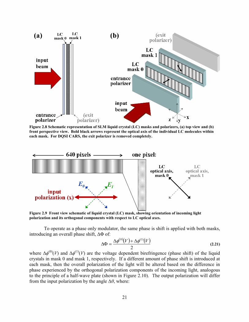
21
Figure 2.8 Schematic representation of SLM liquid crystal (LC) masks and polarizers, (a) top view and (b)
front perspective view. Bold black arrows represent the optical axis of the individual LC molecules within
each mask. For DQSI CARS, the exit polarizer is removed completely.
Figure 2.9 Front view schematic of liquid crystal (LC) mask, showing orientation of incoming light
polarization and its orthogonal components with respect to LC optical axes.
To operate as a phase only modulator, the same phase is shift is applied with both masks,
introducing an overall phase shift, ΔΦ of:
2
)1(0 VV (2.21)
where Δϕ(0)
(V) and Δϕ(1)
(V) are the voltage dependent birefringence (phase shift) of the liquid
crystals in mask 0 and mask 1, respectively. If a different amount of phase shift is introduced at
each mask, then the overall polarization of the light will be altered based on the difference in
phase experienced by the orthogonal polarization components of the incoming light, analogous
to the principle of a half-wave plate (shown in Figure 2.10). The output polarization will differ
from the input polarization by the angle Δθ, where:
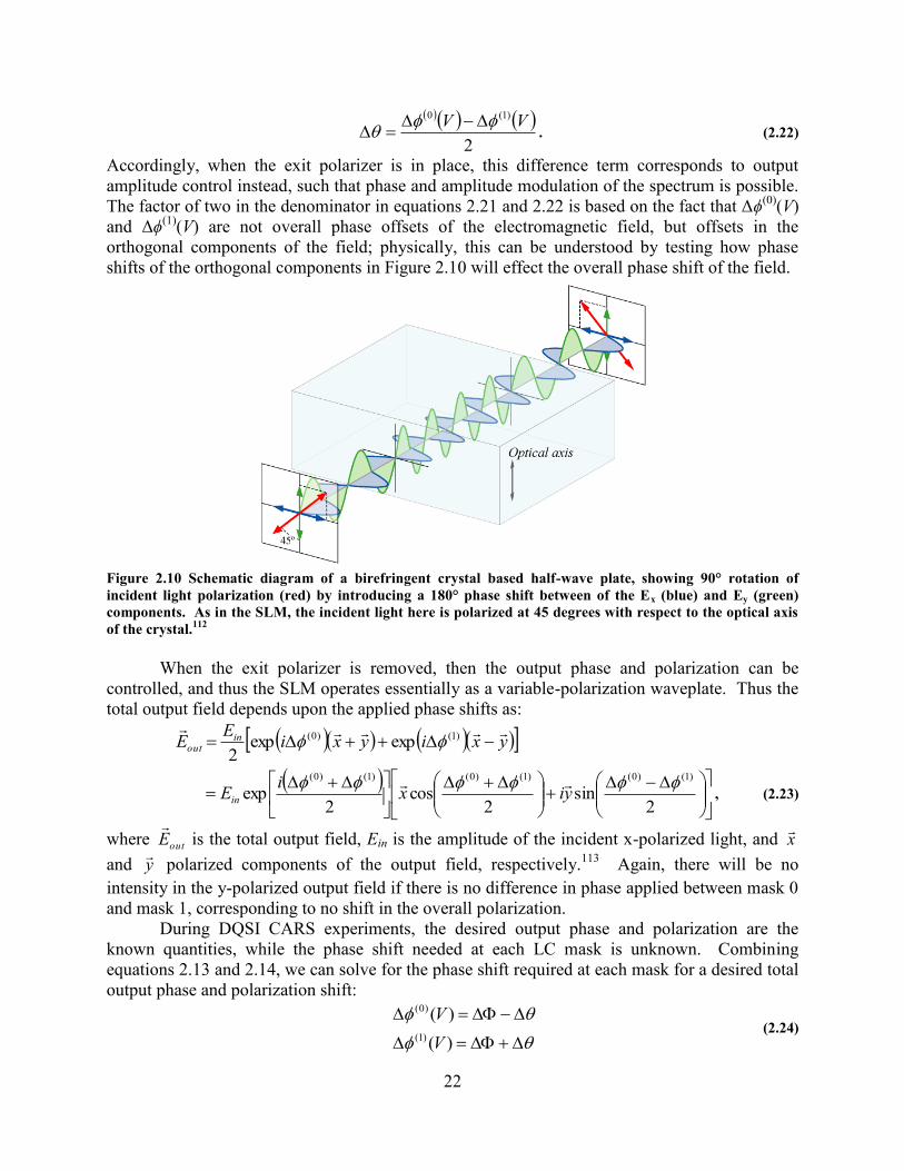
22
2
)1(0 VV
. (2.22)
Accordingly, when the exit polarizer is in place, this difference term corresponds to output
amplitude control instead, such that phase and amplitude modulation of the spectrum is possible.
The factor of two in the denominator in equations 2.21 and 2.22 is based on the fact that Δϕ(0)
(V)
and Δϕ(1)
(V) are not overall phase offsets of the electromagnetic field, but offsets in the
orthogonal components of the field; physically, this can be understood by testing how phase
shifts of the orthogonal components in Figure 2.10 will effect the overall phase shift of the field.
Figure 2.10 Schematic diagram of a birefringent crystal based half-wave plate, showing 90° rotation of
incident light polarization (red) by introducing a 180° phase shift between of the Ex (blue) and Ey (green)
components. As in the SLM, the incident light here is polarized at 45 degrees with respect to the optical axis
of the crystal.112
When the exit polarizer is removed, then the output phase and polarization can be
controlled, and thus the SLM operates essentially as a variable-polarization waveplate. Thus the
total output field depends upon the applied phase shifts as:
yxiyxiE
E inout
)1()0( expexp
2
2sin
2cos
2exp
)1()0()1()0()1()0( yix
iEin
, (2.23)
where outE
is the total output field, Ein is the amplitude of the incident x-polarized light, and x
and y
polarized components of the output field, respectively.113
Again, there will be no
intensity in the y-polarized output field if there is no difference in phase applied between mask 0
and mask 1, corresponding to no shift in the overall polarization.
During DQSI CARS experiments, the desired output phase and polarization are the
known quantities, while the phase shift needed at each LC mask is unknown. Combining
equations 2.13 and 2.14, we can solve for the phase shift required at each mask for a desired total
output phase and polarization shift:
)(
)(
)1(
)0(
V
V (2.24)

23
For example, if no phase shift and 90° polarization change is desired, the phase difference
between mask 0 and 1 should be 180°, requiring Δϕ(0)
= +90° and Δϕ(1)
= -90°. The actual value
sent to the SLM is a voltage, so to achieve the desired phase shift at each LC pixel, a careful
calibration of the voltage-to-phase response of each LC mask is required with the SLM in its
precise, final position within the pulse shaper.113
As mentioned previously, one important role of the pulse shaper and SLM is to compress
the spectral phase at the sample position. When an ultrafast pulse of light passes through any
medium, it acquires a frequency dependent phase shift (spectral phase), which corresponds to a
stretching of the pulse in time, called chirp. The total spectral phase Φ(ω) can be approximated
by a Taylor expansion about ω0, the central frequency of the laser spectrum:
...!4
1
!3
1
!2
1 4
04
3
03
2
02010 (2.25)
where ϕn is the nth
order spectral phase. Taking the first derivative of the spectral phase gives the
group delay, g :
d
dg
)( . (2.26)
The analogous quantity to the group delay in the time domain is the instantaneous frequency or
chirp, ω(t), defined as the first derivative of the temporal phase, ϕ(t):
dt
tdt
)()( 0
. (2.27)
Thus the chirp is always of order n-1; that is, 2nd
order spectral phase corresponds to “linear
chirp,” 3rd
order to “quadratic chirp,” and so on. More chirp (positive or negative) stretches the
pulse temporally, resulting in lower peak power. The microscope objective induces not only
second order spectral phase (linear chirp), which can be compressed by translating the 2nd
grating
of the pulse shaper (Figure 2.4), but also significant higher order spectral phase, which must be
compensated at the microscope focus using the SLM. This chirp is a significant limiting factor
for acquiring broadband CARS spectra, because Raman scattering occurs on timescales the order
of ~1 fs, meaning that both the pump and Stokes pulses (which may be from opposite ends of the
spectrum) must interact with the molecules within that time frame to populate the vibrationally
excited state at SPR (equation 2.8). As is common in discussion of ultrafast pulses, the
term “chirp” will be used when referring to the temporal effects of the spectral phase.
To measure the spectral phase at the sample focus, a procedure called multiphoton
intrapulse interference phase scan (MIIPS) is utilized. Developed by a group at the University of
Michigan for control of multiphoton processes, several comprehensive papers have been
published regarding the theory and practice of the technique.114
Using MIIPS, the unknown
spectral phase is retrieved by measuring the second harmonic generation (SHG) spectrum while
applying a known spectral phase. In the CARS microscope, a 10 μm thick β-barium borate
crystal (BBO, Casix) is placed on a glass coverslip at the microscope focus and the light is
carefully focused within the BBO to maximize the intensity of the second harmonic signal. The
signal is collected with a 0.54 NA objective, followed by a short wave pass filter to remove the
transmitted laser light (740 AESP, Omega Optical) and measured with a fiber-coupled
spectrometer (USB2000, Ocean Optics). Once it is known, the spectral phase is fit to a 4th
order
polynomial and is pre-compensated by applying the opposite spectral phase profile on the SLM.
Then the MIIPS routine is run again, to monitor how well the chirp is compressed by this
spectral phase function; 2-3 iterations of the MIIPS routine are typically required to compress the

24
higher order spectral phase to within ~1 radian, which is more than sufficient for strong CARS
signal intensities.89, 115
The quality of the chirp compression determines the length of the pulse at
the focus; better chirp compression results in a shorter laser pulse at the focus, and therefore
higher peak power per pulse, which results in higher CARS signal and faster HSQ cross-linking
rates. This is explained in more detail in the context of experimental results in chapters 3 and 4.
2.3 Near edge X-ray absorption fine structure (NEXAFS) spectroscopy
Optical microscopy provides resolution on the order of 200-400 nm at best. With much
shorter wavelengths, X-ray microscopy can provide imaging and micro-spectroscopy at
resolutions far exceeding this, as low as 30 nm with current widely-available technology, and the
next generation of microscope technology gives 15 nm resolution.10-12
The power of scanning
transmission X-ray microscopy (STXM) is that it enables mapping of functional group
composition with ~30 nm resolution by acquiring the full NEXAFS spectrum within the tight X-
ray focus.
At X-ray energies near a core shell binding energy of a particular element of interest,
there is an increase in the absorption cross-section, the so-called absorption edge, resulting from
the single-photon ionization of the core electron. The absorption probability near this edge is
further enhanced when the X-ray energy is in resonance with a transition from the core to an
unoccupied molecular orbital (MO), leading to peaks (i.e. fine structure) in the near edge X-ray
absorption spectrum, as shown schematically in Figure 2.11. The spectral features just below
and within about 30 eV above the edge are therefore sensitive to bond angle, length, orientation,
and local bonding environment within the sample, providing a fingerprint of the functional
group(s) within which the element resides.116-117
Note that some unoccupied MOs lie above the
vacuum level/ionization potential, as shown in Figure 2.11 and are therefore referred to as quasi-
bound states. For core-excited molecules, it is also possible for some unoccupied MOs to be
shifted in energy away from their expected ground state configurations; e.g. states lying above
the vacuum level can be shifted below it. Interference between outgoing photoelectrons and
those backscattered from neighboring atoms also leads to energy-dependent oscillations in the
Xray absorption intensity, which decay with increasing energy above the absorption edge.
These oscillations extend out to 100 eV or more above the edge in highly ordered samples such
as diamond and graphite, and so these features are known as the extended X-ray absorption fine
structure (EXAFS) and are a further measure of bond length and long range order in the
sample.116
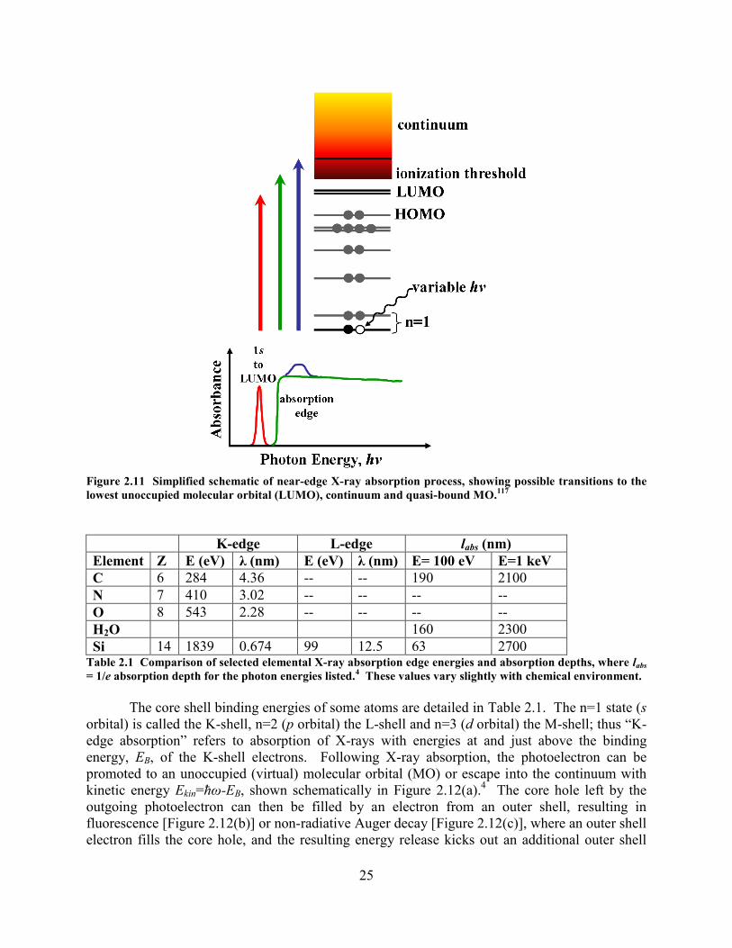
25
Figure 2.11 Simplified schematic of near-edge X-ray absorption process, showing possible transitions to the
lowest unoccupied molecular orbital (LUMO), continuum and quasi-bound MO.117
K-edge L-edge labs (nm)
Element Z E (eV) λ (nm) E (eV) λ (nm) E= 100 eV E=1 keV
C 6 284 4.36 -- -- 190 2100
N 7 410 3.02 -- -- -- --
O 8 543 2.28 -- -- -- --
H2O 160 2300
Si 14 1839 0.674 99 12.5 63 2700 Table 2.1 Comparison of selected elemental X-ray absorption edge energies and absorption depths, where labs
= 1/e absorption depth for the photon energies listed.4 These values vary slightly with chemical environment.
The core shell binding energies of some atoms are detailed in Table 2.1. The n=1 state (s
orbital) is called the K-shell, n=2 (p orbital) the L-shell and n=3 (d orbital) the M-shell; thus “K-
edge absorption” refers to absorption of X-rays with energies at and just above the binding
energy, EB, of the K-shell electrons. Following X-ray absorption, the photoelectron can be
promoted to an unoccupied (virtual) molecular orbital (MO) or escape into the continuum with
kinetic energy Ekin=ħωEB, shown schematically in Figure 2.12(a).4 The core hole left by the
outgoing photoelectron can then be filled by an electron from an outer shell, resulting in
fluorescence [Figure 2.12(b)] or non-radiative Auger decay [Figure 2.12(c)], where an outer shell
electron fills the core hole, and the resulting energy release kicks out an additional outer shell
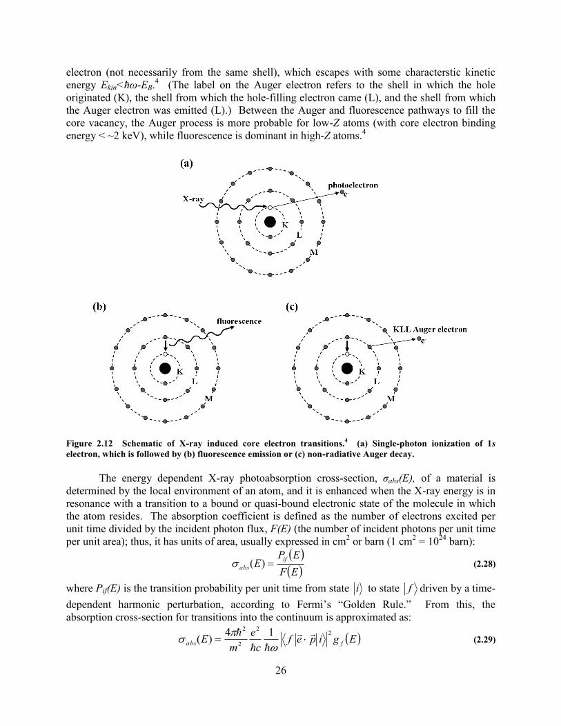
26
electron (not necessarily from the same shell), which escapes with some characterstic kinetic
energy Ekin<ħωEB.4 (The label on the Auger electron refers to the shell in which the hole
originated (K), the shell from which the hole-filling electron came (L), and the shell from which
the Auger electron was emitted (L).) Between the Auger and fluorescence pathways to fill the
core vacancy, the Auger process is more probable for low-Z atoms (with core electron binding
energy < ~2 keV), while fluorescence is dominant in highZ atoms.4
Figure 2.12 Schematic of X-ray induced core electron transitions.
4 (a) Single-photon ionization of 1s
electron, which is followed by (b) fluorescence emission or (c) non-radiative Auger decay.
The energy dependent X-ray photoabsorption cross-section, σabs(E), of a material is
determined by the local environment of an atom, and it is enhanced when the X-ray energy is in
resonance with a transition to a bound or quasi-bound electronic state of the molecule in which
the atom resides. The absorption coefficient is defined as the number of electrons excited per
unit time divided by the incident photon flux, F(E) (the number of incident photons per unit time
per unit area); thus, it has units of area, usually expressed in cm2 or barn (1 cm
2 = 10
24 barn):
EF
EPE
if
abs )( (2.28)
where Pif(E) is the transition probability per unit time from state i to state f driven by a time-
dependent harmonic perturbation, according to Fermi’s “Golden Rule.” From this, the
absorption cross-section for transitions into the continuum is approximated as:
Egipefc
e
mE fabs
22
2
2 14)(
(2.29)
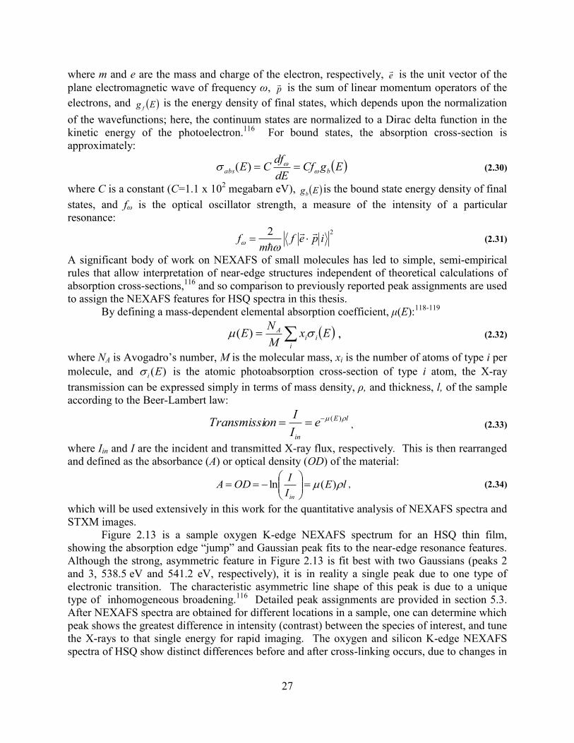
27
where m and e are the mass and charge of the electron, respectively, e
is the unit vector of the
plane electromagnetic wave of frequency ω, p
is the sum of linear momentum operators of the
electrons, and Eg f is the energy density of final states, which depends upon the normalization
of the wavefunctions; here, the continuum states are normalized to a Dirac delta function in the
kinetic energy of the photoelectron.116
For bound states, the absorption cross-section is
approximately:
EgCfdE
dfCE babs
)( (2.30)
where C is a constant (C=1.1 x 10² megabarn eV), Egb
is the bound state energy density of final
states, and fω is the optical oscillator strength, a measure of the intensity of a particular
resonance:
22ipef
mf
(2.31)
A significant body of work on NEXAFS of small molecules has led to simple, semi-empirical
rules that allow interpretation of near-edge structures independent of theoretical calculations of
absorption cross-sections,116
and so comparison to previously reported peak assignments are used
to assign the NEXAFS features for HSQ spectra in this thesis.
By defining a mass-dependent elemental absorption coefficient, μ(E):118-119
ExM
NE
i
iiA )( , (2.32)
where NA is Avogadro’s number, M is the molecular mass, xi is the number of atoms of type i per
molecule, and )(Ei is the atomic photoabsorption cross-section of type i atom, the Xray
transmission can be expressed simply in terms of mass density, ρ, and thickness, l, of the sample
according to the Beer-Lambert law:
lE
in
eI
IonTransmissi )( , (2.33)
where Iin and I are the incident and transmitted X-ray flux, respectively. This is then rearranged
and defined as the absorbance (A) or optical density (OD) of the material:
lEI
IODA
in
)(ln
, (2.34)
which will be used extensively in this work for the quantitative analysis of NEXAFS spectra and
STXM images.
Figure 2.13 is a sample oxygen K-edge NEXAFS spectrum for an HSQ thin film,
showing the absorption edge “jump” and Gaussian peak fits to the near-edge resonance features.
Although the strong, asymmetric feature in Figure 2.13 is fit best with two Gaussians (peaks 2
and 3, 538.5 eV and 541.2 eV, respectively), it is in reality a single peak due to one type of
electronic transition. The characteristic asymmetric line shape of this peak is due to a unique
type of inhomogeneous broadening.116
Detailed peak assignments are provided in section 5.3.
After NEXAFS spectra are obtained for different locations in a sample, one can determine which
peak shows the greatest difference in intensity (contrast) between the species of interest, and tune
the X-rays to that single energy for rapid imaging. The oxygen and silicon K-edge NEXAFS
spectra of HSQ show distinct differences before and after cross-linking occurs, due to changes in

28
the absorption cross-section caused by a modified local bonding structure around the Si and O
atoms.50
Figure 2.13 Representative oxygen K-edge NEXAFS spectrum of HSQ thin film, with Gaussian peak fitting.
Placement of sharp absorption edge “jump” is approximate.
2.4 Scanning transmission X-ray microscopy (STXM)
The experiments presented in chapter 5 were performed at the STXM at beamline 5.3.2
of the Advanced Light Source (ALS) synchrotron at Lawrence Berkeley National Laboratory,
hereafter referred to as the 5.3.2 STXM. The instrument was not designed as part of this work,
and the design details have been previously published.120
An overview of the main components
of the 5.3.2 beamline is shown in Figure 2.14. The X-rays are produced by a bend magnet within
the ALS synchrotron storage ring, providing ~107 photons/s at 250-700 eV (λ = 5.0 nm to
1.8 nm). The photon energy is selected by a monochromator and the Xrays are focused by a
25 nm outer radius Fresnel zone-plate through an order sorting aperture (OSA) to remove higher
order light, resulting in an ~30 nm FWHM beam diameter on the sample. The sample is raster
scanned through the beam focus as the transmitted X-ray flux is detected by a phosphor-coated
Lucite “light pipe” followed by a photomultiplier tube (PMT). Figure 2.15 shows images of the
various components of the 5.3.2 STXM. More detail is given below for select components of
critical importance for these experiments, in the order they are encountered along the beam path.
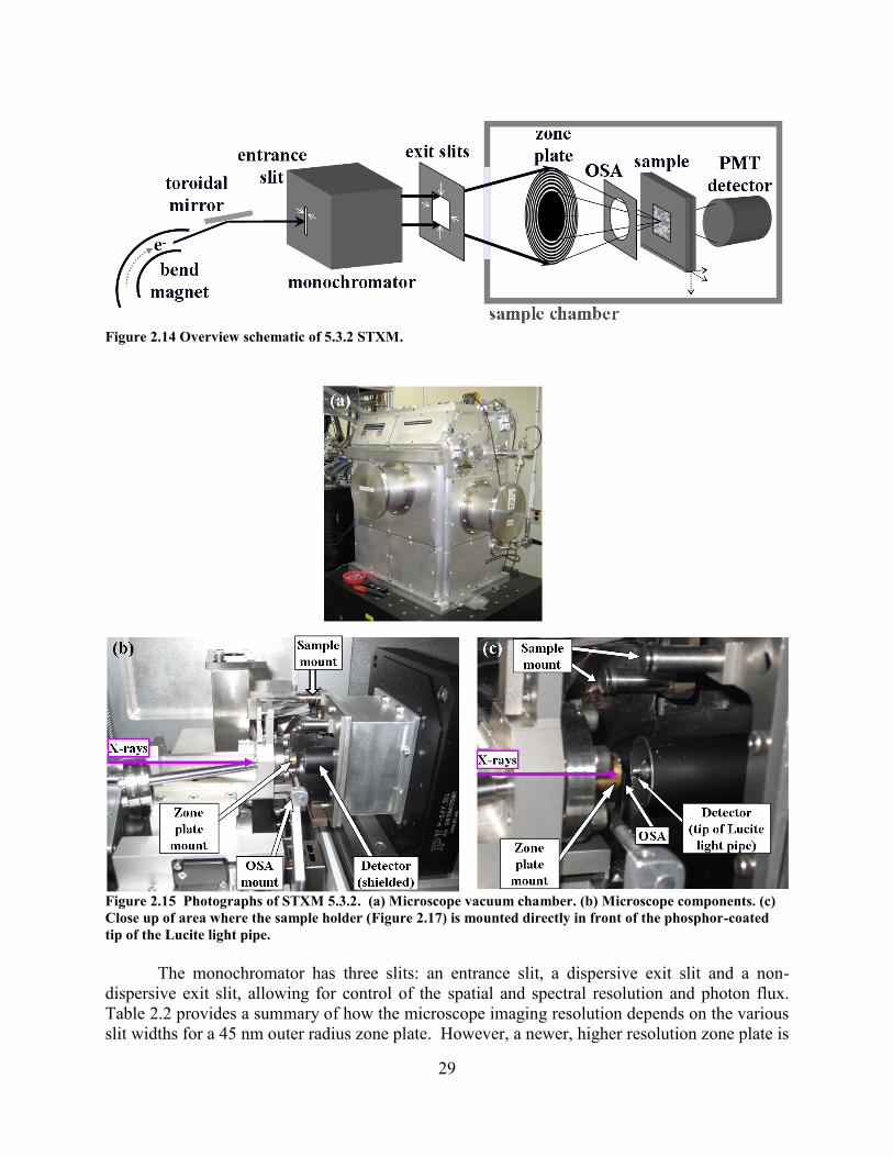
29
Figure 2.14 Overview schematic of 5.3.2 STXM.
Figure 2.15 Photographs of STXM 5.3.2. (a) Microscope vacuum chamber. (b) Microscope components. (c)
Close up of area where the sample holder (Figure 2.17) is mounted directly in front of the phosphor-coated
tip of the Lucite light pipe.
The monochromator has three slits: an entrance slit, a dispersive exit slit and a non-
dispersive exit slit, allowing for control of the spatial and spectral resolution and photon flux.
Table 2.2 provides a summary of how the microscope imaging resolution depends on the various
slit widths for a 45 nm outer radius zone plate. However, a newer, higher resolution zone plate is
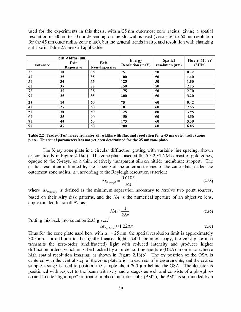
30
used for the experiments in this thesis, with a 25 nm outermost zone radius, giving a spatial
resolution of 30 nm to 50 nm depending on the slit widths used (versus 50 to 60 nm resolution
for the 45 nm outer radius zone plate), but the general trends in flux and resolution with changing
slit size in Table 2.2 are still applicable.
Slit Widths (μm)
Energy
Resolution (meV)
Spatial
resolution (nm)
Flux at 320 eV
(MHz) Entrance Exit
Dispersive
Exit
Non-dispersive
25 10 35 75 50 0.22
40 25 35 100 50 1.40
50 30 35 125 50 1.80
60 35 35 150 50 2.15
75 35 35 175 50 2.70
90 35 35 200 50 3.20
25 10 60 75 60 0.42
40 25 60 10 60 2.55
50 30 60 125 60 3.95
60 35 60 150 60 4.50
70 40 60 175 60 5.30
90 45 60 200 60 6.85
Table 2.2 Trade-off of monochromator slit widths with flux and resolution for a 45 nm outer radius zone
plate. This set of parameters has not yet been determined for the 25 nm zone plate.
The X-ray zone plate is a circular diffraction grating with variable line spacing, shown
schematically in Figure 2.16(a). The zone plates used at the 5.3.2 STXM consist of gold zones,
opaque to the X-rays, on a thin, relatively transparent silicon nitride membrane support. The
spatial resolution is limited by the spacing of the outermost zones of the zone plate, called the
outermost zone radius, Δr, according to the Rayleigh resolution criterion:
NArRayleigh
610.0 (2.35)
where Rayleighr is defined as the minimum separation necessary to resolve two point sources,
based on their Airy disk patterns, and the NA is the numerical aperture of an objective lens,
approximated for small NA as:
rNA
2
(2.36)
Putting this back into equation 2.35 gives:4
rrRayleigh 22.1 . (2.37)
Thus for the zone plate used here with Δr = 25 nm, the spatial resolution limit is approximately
30.5 nm. In addition to the tightly focused light useful for microscopy, the zone plate also
transmits the zero-order (undiffracted) light with reduced intensity and produces higher
diffraction orders, which must be blocked by an order sorting aperture (OSA) in order to achieve
high spatial resolution imaging, as shown in Figure 2.16(b). The xy position of the OSA is
centered with the central stop of the zone plate prior to each set of measurements, and the coarse
sample z-stage is used to position the sample about 200 μm behind the OSA. The detector is
positioned with respect to the beam with x, y and z stages as well and consists of a phosphor-
coated Lucite “light pipe” in front of a photomultiplier tube (PMT); the PMT is surrounded by a
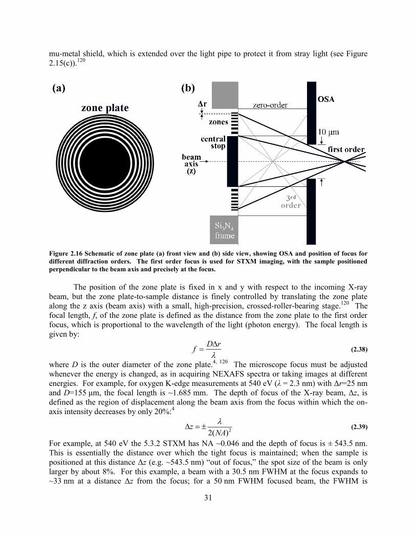
31
mu-metal shield, which is extended over the light pipe to protect it from stray light (see Figure
2.15(c)).120
Figure 2.16 Schematic of zone plate (a) front view and (b) side view, showing OSA and position of focus for
different diffraction orders. The first order focus is used for STXM imaging, with the sample positioned
perpendicular to the beam axis and precisely at the focus.
The position of the zone plate is fixed in x and y with respect to the incoming Xray
beam, but the zone plate-to-sample distance is finely controlled by translating the zone plate
along the z axis (beam axis) with a small, high-precision, crossed-roller-bearing stage.120
The
focal length, f, of the zone plate is defined as the distance from the zone plate to the first order
focus, which is proportional to the wavelength of the light (photon energy). The focal length is
given by:
rDf
(2.38)
where D is the outer diameter of the zone plate.4, 120
The microscope focus must be adjusted
whenever the energy is changed, as in acquiring NEXAFS spectra or taking images at different
energies. For example, for oxygen K-edge measurements at 540 eV (λ = 2.3 nm) with Δr=25 nm
and D=155 μm, the focal length is ~1.685 mm. The depth of focus of the X-ray beam, Δz, is
defined as the region of displacement along the beam axis from the focus within which the on-
axis intensity decreases by only 20%:4
2)(2 NAz
(2.39)
For example, at 540 eV the 5.3.2 STXM has NA ~0.046 and the depth of focus is ± 543.5 nm.
This is essentially the distance over which the tight focus is maintained; when the sample is
positioned at this distance Δz (e.g. ~543.5 nm) “out of focus,” the spot size of the beam is only
larger by about 8%. For this example, a beam with a 30.5 nm FWHM at the focus expands to
~33 nm at a distance Δz from the focus; for a 50 nm FWHM focused beam, the FWHM is

32
~54 nm at Δz. This beam size at different sample depths is very important for Xray patterning
of ~500 nm thick HSQ films, as the size of the Xray beam on the sample determines the pattern
resolution (defined as the minimum possible width for a single-pass line exposure, explained
further in section 5.2).
To transmit some of the Xrays, HSQ samples must be very thin; for the experiments in
this work, HSQ films of 100-500 nm thickness are spin-cast directly onto 100 nm thick silicon
nitride membrane “windows.” More details on HSQ film preparation and characteristics are
presented with experimental results in section 5.2. The commercially available 1 mm × 1 mm,
100 nm thick Si3N4 membrane window (Silson Limited) is produced by back-etching into a
5 mm × 5 mm, 500 μm thick frame, which is shown close up in Figures 2.17(a) and (b). After
coating with HSQ films, the substrates are fixed to a sample holder plate with double-sided tape
as shown in Figure 2.17(c). The sample holder consists of two rows of ~3 mm diameter holes
through which the Xray flux is measured, and each membrane window is thus positioned over
one of these holes. The tape covering these clearance holes is removed prior to sample
mounting.
Figure 2.17 Two views, (a) and (b), of the silicon nitride substrate, a 5x5 mm, 525 μm thick frame with
1x1 mm, 100 nm thick membrane window at center, coated with HSQ thin film. (c) Substrates taped to the
sample holder plate for the 5.3.2 STXM.
To position the sample in the Xray beam, the transmission is measured as the sample is
scanned in x and y (perpendicular to beam axis) with a coarse stepper motor (range 200 μm to
1 mm). When a smaller, well defined region of interest is chosen, the sample fine motion (range
< 200 μm) is controlled by an xy piezo stage. Several different STXM data acquisition modes
are used in this work, controlled by a LabView program with a graphical user interface, detailed
in section 5.2. To focus the X-rays on the sample, the zone plate-to-sample distance is adjusted
to the proper focal length for the precise energy and sample position using a semi-automated
focus scan routine. An “overview” image is taken of an area of interest with an opaque feature,

33
such as the edge of the silicon nitride window or a gold nanoparticle. When the feature is in
focus it will have sharp edges in the image; otherwise, it will be blurry, and the sample to zone-
plate distance must be adjusted. A one-dimensional line scan (along x-axis) is defined by the
user across the feature of interest, as shown in Figure 2.18(a) for focusing across a 100 nm
diameter gold nanoparticle. The STXM software then scans the sample through the beam along
this line repeatedly as the zone plate-to-sample distance is adjusted slightly for each subsequent
scan, as shown in Figure 2.18(b); note how the particle is not visible when this focal distance is
off by more than 5 μm. The range of the zone plate along the z-axis during the focus scan is
defined by the user (typically ~10 to 100 μm range); if the proper focal length is within the scan
range, then at some point during the scan the feature will be in focus, indicated by the black
arrows in Figure 2.18(b), and the zone plate is subsequently fixed at this position. The tightest
focus is possible when the features used have a thickness less than the depth of focus of the beam
(equation 2.41); 100 nm gold particles are ideal for this purpose, and more detail about their use
is given in section 5.2. Typically, for HSQ thin film studies, a rough focus scan with a large z-
axis range (e.g. 100 μm) is followed by a smaller range scan (e.g. 10 μm) to focus the beam to
within ± 500 nm of the film surface, which is within the beam depth of focus. The zone plate
position is adjusted automatically by the instrument when switching to a different photon energy
near the same absorption edge. However, when moving to a new region of the sample or
changing energies by more than ~100 eV, the focus scan is repeated to ensure that tight focusing
is maintained.
Figure 2.18 Example STXM focus scan. (a) Nearly focused image (550 eV) of 100 nm Au nanoparticles and
clusters on HSQ film surface. Bold black arrow points to position of 1D line scan (white line, drawn in). (b)
Resulting focus scan across 1D line as zone-plate-to-sample distance is varied. Black arrows indicate the
relative zone-plate-to-sample distance for optimal focusing.

34
3 Observing multiphoton cross-linking of HSQ with broadband
CARS
This chapter is based on the following publication:
Caster, A.G.; Kowarik, S.; Schwartzberg, A.M.; Nicolet, O.; Lim, S.H.; and Leone, S.R..
Observing hydrogen silsesquioxane cross-linking with broadband CARS. J. Raman Spectrosc.
2009, 40, 770.
Broadband CARS microscopy is used for real-time measurements of in situ cross-linking
of HSQ photoresist films. Using films baked at different temperatures, and therefore cross-
linked to varying degrees, characteristic Raman bands are identified for the open "cage" structure
and cross-linked "network" structure. The first reported multiphoton initiated cross-linking of
HSQ is induced by absorption of high intensity near IR laser light (~1012
W/cm2 peak power).
The sub-second time resolution of broadband CARS is used to follow the laser-induced reaction
in real time by monitoring the characteristic Raman bands, revealing two-stage first order cross-
linking kinetics.
3.1 Introduction: Near infrared multiphoton absorption polymerization of
HSQ
After the e-beam sensitivity of HSQ was first discovered in 1998, researchers noticed that
the areas outside of the e-beam exposed region that were exposed to background electromagnetic
radiation within the e-beam exposure column also became slightly cross-linked.43
Since then,
multiple studies have examined and utilized the sensitivity of HSQ to photons from soft X-rays
(1-2 nm) to the EUV (13.4 nm) and UV (157 nm).41-43, 53-55, 84-85, 121
While previous works show
that cross-linking of HSQ can be induced by absorption of photons up to a wavelength of about
157 nm (7.9 eV per photon), above that wavelength HSQ reportedly exhibited no cross-linking
sensitivity.43
However, several other polymer resists that only absorb at wavelengths in the UV
and below have recently been utilized for multiphoton absorption polymerization (MAP) using
visible and near infrared (NIR) laser sources, and the multiphoton nature of the process leads to a
decrease in the size of features that can be patterned far beyond the diffraction limit.61, 65, 122-125
To investigate the possibility of multiphoton lithography in HSQ, an HSQ thin film is
placed in the CARS microscope described in section 2.2.1, at the focus of the ultrafast pulsed
NIR beam, and MAP is observed in HSQ for the first time. To understand the process in detail,
the cross-linking progress is monitored in real time by following the changes in the CARS peaks
that correspond to the cage and network structures. Comparison to CARS and spontaneous
Raman spectra of thermally cross-linked films confirms that the spectral changes are in fact due
to HSQ cross-linking. By taking spectra in 500 ms intervals during the NIR multiphoton induced
reaction, the initial, fast kinetics are accessible, suggesting a two-stage, first-order cross-linking
mechanism.

35
3.2 Sample preparation and experimental setup
HSQ films are prepared from a flowable oxide solution (FOx-25®, DOW Corning,
1540 wt% HSQ in a volatile methyl siloxane solvent). Thin films are produced by spin-coating
120 μL of the solution onto glass microscope coverslips at 800 RPM for 30 seconds, yielding
films of approximately 1 - 1.2 μm in thickness, as measured with profilometry. Films are cured
on a hot plate in air for 10 min at 150 ºC to evolve any remaining solvent. Measurements are
performed in air, but all samples are stored under high nitrogen flow when not being measured.
For temperature dependent measurements, samples are baked for 10.0 ± 0.5 min at 150 °C,
250 °C, 300 °C, 350 °C and 450 °C (all temperatures are ±15 ºC). The broadband CARS setup
detailed in section 2.2 (Figure 2.3) is used to expose and obtain spectra of the thin films. For
these experiments, a probe centered at 759 nm with a width of ~1 nm is employed,
corresponding to a spectral resolution of about 17 cm-1
. The light is focused on the sample
through a 1.2 NA water-immersion objective (60x UPlanApo, Olympus), and the signal is
collected through a 0.85 NA air objective or 1.0 NA water objective. Homodyne-amplified
CARS spectra are collected with a spectral range of ~250 to 1200 cm-1
, and the region from 300-
650 cm-1
is analyzed to monitor the changing HSQ bands during cross-linking.
Prior to taking spectra, the spectral phase is compressed with the appropriate phase mask
on the SLM, as discussed in section 2.2.2. The average beam power is 46 mW before the
microscope, focused to a diffraction limited spot of ~400 nm diameter, and the transform-
limited, shortest possible pulse duration with the measured laser bandwidth is ~15 fs. This
corresponds to an approximate peak intensity of 2.7 x 10¹³
W/cm2 if the full power reaches the
focus. However, the mirror and microscope objective also reduce the average power by ~50%,
and autocorrelation measurements reveal that pulse compression before the microscope (2nd
order spectral phase, only) results in a pulse duration of ~38 fs. Using MIIPS for pulse
compression at the microscope focus, the pulse duration is likely similar or slightly longer,
resulting in an approximate peak intensity of ≤ 5.4 x 10¹²
W/cm2 at the microscope focus within
the sample.
Spontaneous Raman spectra of the unbaked and baked HSQ thin films are measured in a
home-built microscope with a 10 mW, 633 nm HeNe laser source and 100x, 0.95 NA air
objective. The spectra shown later, in Figure 3.5, are acquired with a more sensitive state-of-the-
art commercial Raman microscope (alpha500, Witec) with a 532 nm laser (38 mW) also focused
through a 100x, 0.95 NA objective (Nikon), and the signal is collected back through the same
objective. Raman depolarization spectra are measured on this microscope by placing a
polarization filter in the beam collection path, which is oriented to transmit the scattered light
polarized either parallel or perpendicular to the input laser polarization.
3.3 Measuring real-time cross-linking kinetics
Figure 3.1(a) shows CARS spectra for HSQ films baked for 10 minutes at temperatures
of 150 °C, 250 °C, 300 °C, and 450 °C. Clear spectral changes are visible with increasing baking
temperature, demonstrating the chemical sensitivity of CARS with respect to the HSQ
microstructure. The film baked at 150 °C corresponds primarily to the nominal cage structure, as
established in previous studies of thermal curing of HSQ, which show that the HSQ cages cross-
link to the network structure only upon heating above 190 ºC.36, 126
With increasing baking
temperature, and therefore increased cross-linking, Raman bands at 342 cm-1
, 454 cm-1
, and

36
562 cm-1
disappear, while a band characteristic of the network structure grows in at 484 cm-1
. In
order to identify the Raman bands in the cage and cross-linked HSQ, Raman spectra are
measured for films baked at 150 ºC as well as 350 ºC for 10 min, shown in Figure 3.2. The
acquisition time for each of these spontaneous Raman spectra was 60 seconds. Comparison of
the CARS spectra in Figure 3.1(a) to spontaneous Raman spectra in Figure 3.2 demonstrates very
good agreement of peak positions and lineshapes in the region from 300-650 cm-1
(although the
CARS wavenumber calibration is likely ~12 cm-1
too low), showing that the homodyne-
amplified CARS spectra are equivalent to the spontaneous Raman spectra within this range.
(However, outside of the 300-650 cm-1
range, there are significant differences between the
DQSI-CARS and spontaneous Raman spectra, which are explored in detail in section 3.4.)
Furthermore, the comparison demonstrates the higher sensitivity of the broadband CARS, which
requires integration times of only 1 s for the spectra in Figure 3.1(a), as opposed to 60 seconds
for the spontaneous Raman with comparable signal-to-noise ratios in Figure 3.2. (The more
sensitive commercial Raman microscope can achieve similar signal-to-noise in ~30 s, shown in
the following section (Figure 3.5).)
In a second set of experiments, CARS spectra are obtained in 50 ms intervals as the HSQ
film remains in the beam focus, in order to study the kinetics of near IR cross-linking, as shown
in Figure 3.1(b). In contrast to curing the films at different temperatures for Figure 3.1(a), the
changes in Figure 3.1(b) are induced by focusing the near IR beam into a diffraction limited
volume, with an approximate peak intensity of 5x10¹²
W/cm2, as noted above. For improved
signal-to-noise, the spectra shown in Figure 3.1(b) are the average of 10 spectra (50 ms each,
total 500 ms acquisition time) which is still fast compared to the timescales of cross-linking.
With increasing near IR exposure time, spectral changes occur similar to those observed upon
baking of the HSQ films, demonstrating that absorption of the intense NIR light does induce
HSQ cross-linking, although possibly by a different mechanism.
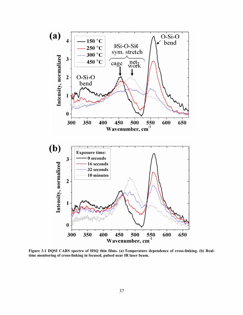
37
Figure 3.1 DQSI CARS spectra of HSQ thin films. (a) Temperature dependence of cross-linking. (b) Real-
time monitoring of cross-linking in focused, pulsed near IR laser beam.

38
Figure 3.2 Spontaneous Raman spectra of HSQ thin films baked for 10 minutes at 150 °C or 350 °C.
A clear isosbestic point at 535 cm-1
in Figure 3.1(b) suggests the loss of one species and
the growth of another. The thermally cross-linked spectra (Figure 3.1(a) and Figure 3.2) are
obtained from different (identical) films, but are likewise normalized from 0 to 1 at 535 cm-1
. By
comparing the spectra in Figure 3.1(a) and (b), one sees that the amount of conversion to the
network structure after 10 minutes of near IR exposure is greater than for the sample heated to
300 ºC for 10 minutes. Since it has been reported that HSQ does not have any direct sensitivity
to cross-linking under near IR exposure,43
multiphoton absorption and heating in the focus of the
intense beam are considered as two possible conversion mechanisms. At the powers used, some
heating of the sample is expected in the beam focus, but note that a temperature of at least
190 °C must be reached to initiate significant bond redistribution in HSQ.11
To determine if
heating is the primary mechanism, the cross-linking rate is measured again using a water
immersion collection objective. If heating plays a significant role in the cross-linking, water is
expected to slow the cross-linking by better thermal removal of the heat, thus resulting in a lower
temperature within the focal volume. However, it is observed that when water is in contact with
the sample during exposure, the cross-linking rate does not change. Furthermore, it is observed
that when the average laser power is reduced by half, the rate for the initial stage of cross-linking
decreased by approximately a factor of ten. This implies a strongly non-linear process,
suggesting that the primary cross-linking mechanism in the laser focus is MAP, which will be
explored in more detail in Chapter 4.
The peaks in the CARS spectra of non-cross-linked (cage) HSQ can be assigned based on
observations and calculations reported by Bornhauser and Calzaferri.127
However, previous
Raman assignments for cross-linked (network) HSQ thin films are not available. Furthermore,
all previously reported Raman studies were performed on pure (powdered) HSQ solids rather
than the thin films, which have slightly different characteristics. For the non-cross-linked HSQ
films, the 342 cm-1
and 562 cm-1
peaks are assigned to OSiO bends, compared to spontaneous

39
Raman spectroscopy values of 341 cm-1
and 576 cm-1
(calculated).127
The 454 cm-1
peak is
assigned to the symmetric stretch, compared to 446 cm-1
(calc.).127
The three bond
symbol, , represents all the other cage-like or network-like bonds to the silicon atom.
After 10 minutes of near IR exposure, the O-Si-O bend peaks at 342 cm-1
and 562 cm-1
decrease to about 25 % of their original intensity, as does the symmetric stretch at
454 cm-1
, while a new peak at 484 cm-1
emerges. As the HSQ cages cross-link, the structure
becomes more and more like that of SiO2 (SiO4/2), as bonds replace bonds.35
The loss of the OSiO bending peaks is attributed to the change of the cage OSiO bonds, with
an angle of approximately 109.5º,127
to the network OSiO bonds, which are possibly more
linear and rigid compared to the cage bonds. The 484 cm-1
peak is tentatively assigned to a
symmetric stretch after cross-linking, as FTIR spectra show that the stretch
grows in as the network structure forms,35
and there is a known IR active symmetric
stretch for cage HSQ at 481 cm-1
,127
which may become Raman active in the network structure
due to changes in symmetry. Furthermore, an increased rigidity of bonds in the
network structure can explain the increase of the stretching wavenumber from 454 cm-1
. This
increasing rigidity can be pictured using a physical model of the monomer cage, which is free to
stretch and compress in almost any direction, while the cross-linked cages become more fixed in
their positions as they form more bonds to other cages and the existing network. Also, the
484 cm-1
peak is substantially more broad (FWHM 61 cm-1
) than the initial 454 cm-1
peak
(FWHM 30 cm-1
), which may be due to the fact that network O-Si-O bonds have a variety of
possible angles and bond lengths (including some remaining cage-like bonds) at different cross-
linked sites,35
leading to inhomogeneous broadening of the spectral linewidth.
For a more detailed analysis of the kinetics of cross linking, the peaks in the spectra in
Figure 3.1(b) are fit to a Gaussian profile to determine the area of the 454 cm-1
, 484 cm-1
, and
562 cm-1
CARS bands. Figure 3.3 shows the decay of the 562 cm-1
peak (OSiO bend)
characteristic of the cage structure, and the rise of the peak at 484 cm-1
( symmetric
stretch) characteristic of the network structure, from 0 to 10 minutes. The data is best fit by a
double exponential decay, with a fast initial time constant (decay lifetime, τ1) of 24.4 ± 1.3
seconds for the decay of the OSiO bend and the increase of the network stretch,
demonstrating a direct conversion from cage to network structure without long lasting
intermediate species. The second stage of the HSQ cross-linking kinetics occurs on a much
slower timescale for which the fit gives different constants (τ2) of 221 ± 16 seconds for the decay
and 123 ± 11 seconds for the growth, with the difference probably due to fit uncertainties and
neglecting inhomogeneous broadening. The decay lifetime, τ, for each stage is defined as the
time at which 1/e (37%) of the cage-like peak area remains. This data set was reproduced on
different days with several different HSQ thin film samples, with time constants for the initial,
fast regime ranging between 10 seconds and 30 seconds. The variability in the experiment is
most likely due to variations in the film thickness and, more critical, differences in laser peak
intensity due to incomplete chirp compression, which will be discussed in more detail in section
4.3.

40
Figure 3.3 Decay of the 562 cm
-1 peak area (cage-like O-Si-O bend) with time in the focused near IR beam,
and growth of the 484 cm-1
band (network-like symmetric stretch). Solid lines are double
exponential decay fit. Both the decay and growth kinetics exhibit a fast first stage with a time constant of
~24 s and a much slower second stage.
Zero, first and second order kinetics were considered for each stage of the measurements
in Figure 3.3 and several similar measurements, and two-stage, first order kinetics (in the rate
limiting step) best explains the double exponential decay curves. In previously reported
photoinduced polymerization reactions, first-order kinetics were also observed, which was
expected when a fixed concentration of photoinitiator molecules is initially present.128
In HSQ,
cross-linking may proceed by the network conversion of a limited number of reactive sites in the
as-spun film (prior to exposure), where the atoms have approximately the optimal relative
orientation and juxtaposition for network formation. The two first-order stages of cross-linking
with exposure time (at constant laser power) can then be explained if there is an initial
concentration of easily cross-linked sites, which react quickly, leaving a only some less favorable
reaction sites that result in the much slower, second stage of the reaction, possibly by a slightly
different mechanism. This two-stage cross-linking kinetics of HSQ has also been observed in
multiple experiments in our laboratories by using X-ray induced cross-linking and X-ray
spectroscopic detection, which will be discussed in detail in Chapter 5.
Different cross-linking mechanisms have been proposed for ebeam and thermally
induced cross-linking of HSQ, but the end result of each mechanism is an increase in the to
ratio of the exposed or heated film. For thermally-induced cross-linking of HSQ above the
onset of curing at ~190º C,36, 126, 129
redistribution of the network leading ultimately to SiO4/2
bond formation and evolution of silane gas (SiH4) is the primary mechanism proposed for curing
from ~250-350 ºC. Remaining bonds within the network structure create the porosity that
gives the network HSQ its low dielectric constant. Two-stage, zero-order kinetics58
have
previously been proposed for the low temperature reaction (250350 ºC). In that work, the
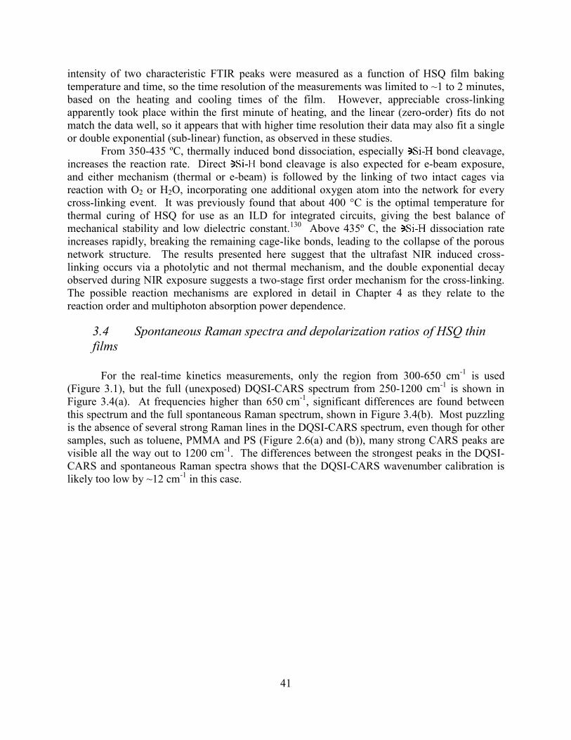
41
intensity of two characteristic FTIR peaks were measured as a function of HSQ film baking
temperature and time, so the time resolution of the measurements was limited to ~1 to 2 minutes,
based on the heating and cooling times of the film. However, appreciable cross-linking
apparently took place within the first minute of heating, and the linear (zero-order) fits do not
match the data well, so it appears that with higher time resolution their data may also fit a single
or double exponential (sub-linear) function, as observed in these studies.
From 350-435 ºC, thermally induced bond dissociation, especially bond cleavage,
increases the reaction rate. Direct bond cleavage is also expected for ebeam exposure,
and either mechanism (thermal or ebeam) is followed by the linking of two intact cages via
reaction with O2 or H2O, incorporating one additional oxygen atom into the network for every
cross-linking event. It was previously found that about 400 °C is the optimal temperature for
thermal curing of HSQ for use as an ILD for integrated circuits, giving the best balance of
mechanical stability and low dielectric constant.130
Above 435º C, the dissociation rate
increases rapidly, breaking the remaining cage-like bonds, leading to the collapse of the porous
network structure. The results presented here suggest that the ultrafast NIR induced cross-
linking occurs via a photolytic and not thermal mechanism, and the double exponential decay
observed during NIR exposure suggests a two-stage first order mechanism for the cross-linking.
The possible reaction mechanisms are explored in detail in Chapter 4 as they relate to the
reaction order and multiphoton absorption power dependence.
3.4 Spontaneous Raman spectra and depolarization ratios of HSQ thin
films
For the real-time kinetics measurements, only the region from 300-650 cm-1
is used
(Figure 3.1), but the full (unexposed) DQSI-CARS spectrum from 250-1200 cm-1
is shown in
Figure 3.4(a). At frequencies higher than 650 cm1
, significant differences are found between
this spectrum and the full spontaneous Raman spectrum, shown in Figure 3.4(b). Most puzzling
is the absence of several strong Raman lines in the DQSI-CARS spectrum, even though for other
samples, such as toluene, PMMA and PS (Figure 2.6(a) and (b)), many strong CARS peaks are
visible all the way out to 1200 cm-1
. The differences between the strongest peaks in the DQSI-
CARS and spontaneous Raman spectra shows that the DQSI-CARS wavenumber calibration is
likely too low by ~12 cm-1
in this case.
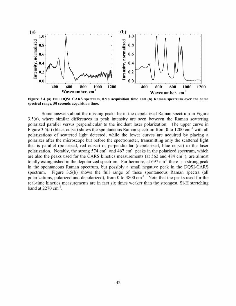
42
Figure 3.4 (a) Full DQSI CARS spectrum, 0.5 s acquisition time and (b) Raman spectrum over the same
spectral range, 50 seconds acquisition time.
Some answers about the missing peaks lie in the depolarized Raman spectrum in Figure
3.5(a), where similar differences in peak intensity are seen between the Raman scattering
polarized parallel versus perpendicular to the incident laser polarization. The upper curve in
Figure 3.5(a) (black curve) shows the spontaneous Raman spectrum from 0 to 1200 cm1
with all
polarizations of scattered light detected, while the lower curves are acquired by placing a
polarizer after the microscope but before the spectrometer, transmitting only the scattered light
that is parallel (polarized, red curve) or perpendicular (depolarized, blue curve) to the laser
polarization. Notably, the strong 574 cm-1
and 467 cm-1
peaks in the polarized spectrum, which
are also the peaks used for the CARS kinetics measurements (at 562 and 484 cm-1
), are almost
totally extinguished in the depolarized spectrum. Furthermore, at 697 cm-1
there is a strong peak
in the spontaneous Raman spectrum, but possibly a small negative peak in the DQSI-CARS
spectrum. Figure 3.5(b) shows the full range of these spontaneous Raman spectra (all
polarizations, polarized and depolarized), from 0 to 3800 cm-1
. Note that the peaks used for the
real-time kinetics measurements are in fact six times weaker than the strongest, Si-H stretching
band at 2270 cm-1
.
43
Figure 3.5 Spontaneous Raman spectra of ~1 μm thick HSQ film pre-baked at 150 °C for 10 minute. (a)
Region accessible with DQSI CARS, and (b) full spectrum. All scattered polarizations are detected for the
upper curves (black), but polarized signal only is detected for the middle curves (red), and the bottom curves
(blue) are the depolarized spectra.

44
The ratio of the depolarized to polarized peak intensity in Raman scattering spectroscopy
depends upon the symmetry of each particular vibrational mode. The Raman depolarization ratio
for a single vibrational mode is defined as:
parallel
larperpendicu
dI
I (3.1)
where Iperpendicular and Iparallel are the intensity of the light scattered perpendicular and parallel to
the laser polarization, respectively,86
and the total scattering signal using these definitions is
approximately Iperpendicular + Iparallel. Thus, vibrational modes that depolarize the light have a large
depolarization ratio, and peaks with a small depolarization ratio are said to be highly polarized.
More specifically, the depolarization ratio for totally symmetric vibrational modes is always less
than 0.75, and these are called polarized bands, while all other modes should exhibit
depolarization ratios of ~0.75, and are thus called depolarized.86
The 574 cm-1
and 467 cm-1
bands, assigned to the OSiO bend and symmetric stretch, respectively, and the broad
(overlapping) bands from 200-400 cm-1
are all highly polarized, with depolarization ratios of
≤0.15, and thus are totally symmetric vibrational modes. This is in agreement with the
calculated point group for each of these modes; as shown in Table 3.1, the 574 and 467 cm-1
bands correspond to normal modes with A1g point group symmetry. The remaining peaks
between 574 cm-1
and 1200 cm-1
all exhibit depolarization ratios of ~0.75, and thus they are not
totally symmetric modes. Therefore, it appears that only the totally symmetric modes are
observed in the DQSI-CARS spectra.
It is likely that most of depolarized signal is lost in the projection (splitting) and
subtraction steps of DQSI-CARS (equations 2.16 and 2.19 and Figure 2.5). For totally
symmetric modes, which are highly polarized, most of the resonant CARS signal will be
scattered at the same polarization as the probe field, which is assumed for the projection
equations (2.16). However, for depolarized modes, 3/4 as much light is scattered perpendicular
to the probe polarization; that is to say, ~43% [or 43
43 1 ] of the scattered light is polarized
perpendicular and ~57% [or 4311 ] parallel to the laser polarization. Assuming these
depolarization ratios for the non-totally symmetric Raman modes, in the projection step these
(non-symmetric) peaks only will not follow equation 2.16, but instead:
R
i
R PP2
1 and RR
j
R PPP 1.012
1
43
41
(3.2)
where RP is the total resonant CARS signal, given by equation 2.13. Thus, unlike for equations
2.16, the resonant signal in spectrum j is no longer equal in magnitude to that in spectrum i, and
following equations 2.17 through 2.19, the total difference signal for the depolarized (non-
symmetric) modes only is:
PrPrPr
43
41
sinImcosRe12
1 LLAPSS NRR
ji
(3.3)
Here, the pre-factor in the difference signal is just ~0.07, compared to a value of 2 in equation
2.19, which has proven to be valid only for totally symmetric Raman modes; thus, only ~4% as
much signal is collected for depolarized peaks as for polarized ones! Furthermore, there is also a
possibility that some signal is lost in the scattering process itself based on the symmetry of the
peaks; as the pump and Stokes fields are parallel in polarization, it is feasible that they do not
coherently excite the depolarized oscillations as effectively as the polarized ones. However, to
fully understand the DQSI-CARS depolarization effect on the scattering intensity will require

45
theoretical treatment of the third-order nonlinear susceptibility (a fourth-rank tensor) with respect
to the polarization of the pump and probe fields and the symmetry of the vibrational modes.
Instead, other variations of broadband CARS that use phase-shaping techniques only, such as
Fourier-transform spectral interferometry (FTSI) CARS,131
can be used in the future to
circumvent these polarization effects. However, for the HSQ kinetics measurements in this
study, the peaks from 300 to 650 cm-1
are sufficient to assess the degree of cross-linking.
The Raman and CARS peak values and assignments for the HSQ thin films are
summarized in Table 3.1. The previously reported HSQ Raman have all been for powdered,
crystalline HSQ, which show some differences in peak positions and intensities from the thin
films. This supports earlier reports of structural differences that occur upon spin coating of
HSQ, even under vacuum at room temperature,47, 132
and could also be due to slight chemical
differences of the HSQ used in the Dow Corning spin-on solution.
Peak assignments, present work
HSQ thin film Source of assignment, literature
Observed
(cm-1
) Type of
Vibration
(ν=stretch,
δ=bend)**
polarized
or
depolarized
(ratio)
Ref.
#
Type of
sample
Observed
(calculated)
(cm-1
)
Ra
ma
n o
r IR
act
ive
(R,
IR) Type of
Vibration
(ν=stretch,
δ=bend)
Symmetry Spont.
Raman
(relative
strength)*
DQSI-
CARS
165 (w) n/a δ(OSiO)cage depol (5) 127
HSQ powder 171 (168) R δ(OSiO) T2g
364 (w) 342 δ(OSiO)cage pol (0.15) 133
HSQ powder (341) R δ(OSiO) T2g 127
HSQ powder 399 (397) IR δ(OSiO) T1u
414 (vw) -- 127
HSQ powder 414 (418) R δ(OSiO) T2g
HSQ powder 423 (423) R δ(OSiO) Eg
467 (m) 454 νs(SiOSi)cage pol (0.07) 127
HSQ powder 446 (456)
456 (456) R νs(SiOSi) A1g
-- 484 νs(SiOSi)network --
127
133
HSQ powder 468 (468) IR νs(SiOSi) T1u
HSQ powder 465 (481) IR νs(SiOSi) T1u
574 (s) 562 δ(OSiO)cage pol (0.05) 133
HSQ powder 580 (576) R δ(OSiO) A1g
HSQ powder 610 (613) R νs(SiOSi) T2g
697 (s) NONE νs(SiOSi) depol (0.75) 127
HSQ powder 697 (691) R νs(SiOSi) Eg
833 (m) NONE δ(SiOH) ? depol (0.72)
134
(CH3)3SiOH
(theory) (832) --
δ(SiOH) 135
3-aminopropyl-
triethoxysilane 840 R
136 silica 840
137 silica 834 IR
30
“T14”
(HSiO3/2)14 830 IR δ(OSiH) ?
894 (s) NONE δ(OSiH) depol (0.79) 133 HSQ powder 890 (894) R δ(OSiH) T2g
925 (s) NONE δ(OSiH) depol (0.77) 133 HSQ powder 932 (922) R δ(OSiH) Eg
1067 (vw) NONE νas(SiOSi) -- 133 HSQ powder 1117 (1116) R νas(SiOSi) T2g
1146 (vw) NONE νas(SiOSi) -- 133 HSQ powder 1141 (1143) IR νas(SiOSi) T1u
1270 (vw) n/a
solvent ? --
138 Si(OC2H5)4 (l)
1295 R
1306 (vw) n/a --
1350 (vw) n/a pol (~0)

46
1453 (vw) n/a
δ(SiOH)
depol (~1)
139
uranyl
silicates 1453 R
δ(SiOH)
δas(CH3)
δas(CH3)
(solvent) 138
Si(OC2H5)4 (l) 1458 R
1606 (vw) n/a ? depol (~1)
1652 (vw) n/a ? depol (~1) 138
silica gel 1635 R
1736 (vw) n/a ? depol (0.87)
1805 (vw) n/a ? depol (0.87)
1894 (vw) n/a solvent ? pol (~0) 138
Si(OC2H5)4 (l) 1895 IR
2271 (vs) n/a ν(SiH) pol (0.17)
133 HSQ powder 2277 (2381) IR ν(SiH) T1u 133 HSQ powder 2291 (2381) R ν(SiH) T2g 133 HSQ powder 2302 (2381) R ν(SiH) A1g
2865 (vw) n/a solvent ? pol (~0) 138
Si(OC2H5)4 (l) 2870 R
2908 (w) n/a νs(CH3)
(solvent) pol (0.19)
134 (CH3)3SiOH 2906 (pol)
R νs(CH3) 135
3-aminopropyl-
triethoxysilane 2887,2929
2938 (vw) n/a solvent ? pol (~0) 138
Si(OC2H5)4 (l) 2930 R
2966 (w) n/a νas(CH3)
(solvent) depol (0.70)
134 (CH3)3SiOH 2967 (depol)
R νas(CH3) 135
3-aminopropyl-triethoxysilane 2974
3079 (vw) n/a ? depol (0.84)
3153 (vw) n/a ? depol (0.85)
*Relative peak strength: vw=very weak, w=weak, m=medium, s=strong and vs=very strong.
**νas=anti-symmetric stretch, νs=symmetric stretch.
Table 3.1 Observed Raman and DQSI-CARS spectrum peaks and peak assignments, with corresponding
literature values for similar samples. Peaks highlighted in yellow are used for kinetics analysis in this work.
3.5 Conclusions
With broadband CARS microscopy, cross-linking kinetics are measured in a relatively
novel spin-on dielectric and photoresist material, hydrogen silsesquioxane, in situ in 500 ms
time-intervals. The robust, single beam interferometric method used here to acquire broad
Raman equivalent spectra allows for fast measurements that contain a great deal of spectral
information. These studies show that substantial HSQ cross-linking occurs within the first
minute of focused, pulsed NIR laser exposure, followed by a slower second stage, and proceeds
with apparently first-order kinetics. This discovery opens the possibility for direct-write,
muliphoton lithography (MAP) in HSQ and related materials with visible and NIR laser sources.
The experiments detailed in the following chapter explore the non-linearity of the NIR induced
cross-linking, and possible mechanisms to explain the two stage nature of the cross-linking
process. X-ray microscopy experiments detailed in Chapter 5 further elucidate the photo-intiated
reaction mechanism, also showing that the reaction may follow two-stage first order kinetics, and
gives some insight about which species are involved in the two stages of the reaction.
The first spontaneous Raman spectra of HSQ thin films are presented with peak
assignments, and comparison to the DQSI-CARS spectra reveals that the non-totally symmetric
modes are not accessible with DQSI-CARS. While the totally symmetric modes are sufficient to
monitor the degree of HSQ cross-linking, with new variations of the single beam, broadband
CARS technique, it will be possible to gain more information about not only HSQ, but also the
properties of other rapidly-changing chemical systems.

47
4 Investigating the near-IR multiphoton cross-linking
mechanism of HSQ
The power dependence of the HSQ cross-linking rate in the focused, pulsed near IR laser beam
reveals that at high average powers (>45 mW) the process is initiated by absorption of
approximately 6±1 near IR photons, similar to the amount of energy necessary for UV
lithography at 157 nm, indicating a photoinduced cross-linking mechanism driven by bond
breaking. The cross-linking rate is much slower below this average power threshold, suggesting
a photothermal bond redistribution mechanism at low powers. As a highly nonlinear process, the
multiphoton HSQ cross-linking is very sensitive to spectral phase, or chirp, on the ultrafast pulse,
with a greater than 100-fold increase in cross-linking rate when higher order chirp (3rd
and 4th
order spectral phase) is compressed at the beam focus within the sample. By controlling both the
chirp and laser power, the HSQ cross-linking rate is finely tuned across a wide range of values
while still maintaining a strong CARS signal. Various potential reaction mechanisms are
explored to explain the highly non-linear power dependence and apparent reaction order of the
multiphoton-induced cross-linking.
4.1 Introduction
Recently, features as small as 40 nm have been patterned in polymer photoresists using
focused, pulsed near IR lasers via multiphoton absorption polymerization (MAP).18, 60, 140
With
direct-write multiphoton photolithography, it was even possible to expose and etch positive-tone
resists with the laser in a single step, eliminating the need for post-exposure development.59, 141
Power dependence studies of such processes have shown that they are highly non-linear,
requiring the absorption of up to ~7 photons to initiate each bond breaking event in positive tone
resists, producing features as narrow as 120 nm in PMMA with a single, tightly focused beam of
pulsed 870 nm light (170 fs pulse duration).59, 141
The lithographic resolution enhancement is
greatest for highly nonlinear photoabsorption processes. The near infrared (NIR) induced HSQ
cross-linking rate is very sensitive not only to average laser power but also peak intensity,
indicating that it is a highly non-linear process. Therefore, by utilizing MAP of HSQ, it may be
possible to pattern sub-micron features with direct-write lithography using relatively inexpensive
pulsed NIR lasers. If the resolution is sufficient for microfabrication applications, the lower cost
of the NIR exposure source is a big advantage when compared to the high cost of X-ray, e-beam
and EUV sources otherwise required for patterning of HSQ.
Another particularly exciting application of MAP that cannot be achieved with single-
photon or e-beam exposure processes is the fabrication of 3D micro and nanostructures in thicker
films, such as photonic crystal fibers and 3D optical data storage structures.17, 124, 140
While
HSQ and related materials have not yet been investigated for these applications, exploring the
NIR MAP of HSQ opens the door for new opportunities in complex 3D microstructure
fabrication in HSQ and HSQ-like materials. Understanding the number of NIR photons, and
thus the amount of energy, required to initiate the cross-linking gives a key insight into the
photolytic process, whether it is dominated by or limited, for example, by versus
bond breaking, and this knowledge can be used to fine tune the chemistry of HSQ-like resist
materials for sensitive, high contrast multiphoton lithography, as well as for X-ray, ebeam and
EUV lithography. Furthermore, with the same source used for exposure, broadband CARS

48
spectra are used for in situ analysis of the degree of cross-linking achieved. This is highly
desirable for analyzing the chemistry and structural integrity of polymer microstructures, as
previously demonstrated using narrowband CARS microscopy.75, 142
When the laser power before the microscope is maximized (67 mW average power) and
the higher order chirp is fully compressed with the SLM (~38 fs pulse duration), both the CARS
signal and HSQ cross-linking rate are maximized. However, when only the linear chirp is
compressed, a slightly weaker CARS signal is detected without inducing appreciable HSQ cross-
linking. Upon further investigation, it is evident that the rate of cross-linking is very sensitive to
the degree of chirp, and hence the peak power, of the laser pulses. This suggests that each HSQ
cross-linking event requires more photons, on average, than the third-order CARS process. To
assess the non-linearity of the HSQ cross-linking rate, the pulsed NIR beam is focused into the
HSQ thin film and the rate of decay of the concentration of cage-like HSQ species is measured
repeatedly for different average laser powers, ranging from 34 mW to 67 mW. The cross-linking
rate increases as the average power is increased, and a threshold power is observed above which
the multiphoton non-linearity of the process appears to change, suggesting that there are different
photoconversion mechanisms at low versus high laser power. These results are consistent with
previous reports of multiphoton ablation lithography in positive tone resists.59
The previously
proposed HSQ cross-linking reaction mechanisms are presented in the context of these
observations to explain the non-linear power dependence and apparent first order kinetics of the
cross-linking reaction.
4.2 Sample preparation and experimental setup
Following the same methods as described in the chapter 3, HSQ films are prepared by
spin-coating 200 μL of the flowable oxide solution (FOx-25®, DOW Corning) onto borosilicate
glass microscope coverslips at 830 ± 30 RPM for 30 seconds, yielding films approximately 1 μm
thick. Films are cured on a hot plate in air for 2 min. at 150 ± 5 ºC to evolve any remaining
solvent. Again, the broadband CARS setup detailed in section 2.2.1 and Figure 2.3 is used to
obtain coherent Raman spectra of the thin film samples. The light is focused on the sample
through a 1.2 NA water-immersion objective (60x UPlanApo, Olympus), and the signal is
collected through a 0.85 NA air objective.
As in Chapter 3, homodyne-amplified CARS spectra are collected with a spectral range
of ~250 cm-1
to 1200 cm-1
. The kinetics of the HSQ cross-linking reaction are measured by
focusing the beam into the HSQ thin film and acquiring the CARS spectrum in 500 ms intervals
over a period of ~200 seconds at each laser power. The decay of the 562 cm-1
peak area,
characteristic of the cage-like O-Si-O bend in HSQ, is analyzed versus exposure time, to assess
the relative degree of cross-linking, decay lifetime and cross-linking rate for different laser pulse
conditions. Optimal chirp compression at the microscope focus results in a pulse duration of
~38 fs, which is focused to a diffraction limited spot of ~400 nm diameter. With 67 mW of
average power before the microscope, this corresponds to ≤ 7.8x10¹²
W/cm2 peak power density
at the focus in the sample.
The HSQ cross-linking rate is controlled by adjusting the peak power of the laser at the
microscope focus in two different ways: by adjusting the chirp at constant average laser power,
or adjusting the average laser power with the same (constant) degree of chirp. As described in
section 2.2.2, the chirp is measured immediately prior to inserting the sample by placing a BBO

49
crystal at the microscope focus; linear chirp (2nd
order spectral phase) is compressed by
translating the second grating of the pulse shaper (Figure 2.4(a)) in order to optimize the SHG
signal from the BBO, and the 3rd
and 4th
order spectral phase are then measured using MIIPS.
First, the HSQ cross-linking is measured with only the linear chirp compressed at the microscope
focus. Next, without removing the sample, the higher order chirp (3rd
and 4th
order spectral
phase) is compressed by applying the appropriate phase with the SLM, as determined by the
MIIPS measurement. With compressed pulses, the HSQ cross-linking rate is measured as a
function of average laser power before the microscope, varied from 34.5 mW to 67 mW with a
variable neutral density filter wheel placed just after the pulse shaper. Each measurement is
taken at a single point in the HSQ thin film. Then, the laser power or chirp is adjusted, and the
sample is subsequently translated laterally by ~20 μm to a new spot on same film.
To directly compare cross-linking rates and lifetimes at many different laser powers, the
exact same focusing characteristics and pulse duration (based on the chirp) must be maintained
for each measurement. This is challenging due to long-time drift in the chirp, laser power and
beam pointing stability, so each full set of power dependence measurements (at constant chirp)
was acquired within a period of less than two hours. To accomplish this, the kinetics curves at
each power are measured for less than five minutes (300 seconds) each. Besides the small lateral
shift to a new sample position for each measurement, nothing is changed between subsequent
kinetics measurements in a given data set.
4.3 Dependence of cross-linking rate on peak intensity: chirp effects
For an average laser power of 67 mW before the microscope with only linear chirp
compressed, the decay of the 562 cm1
peak area, and thus the increase in HSQ cross-linking,
proceeds only very slowly, as shown in the upper curve of Figure 4.1(a). By comparison, when
the higher order chirp is compressed with the SLM at the same average laser power, the initial
cross-linking proceeds more than 100 times faster, as shown in the lower curve in Figure 4.1(a).
To directly compare the initial lifetime τ1 of the chirped versus compressed measurements
requires the same normalization for both curves, which is shown in Figure 4.1(b).

50
Figure 4.1 Decay in 562 cm
-1 peak area for a chirped pulse (upper curve, open squares) versus compressed
pulse (lower curve, filled circles) at the focus in the HSQ thin film, (a) raw data, before normalization and (b)
normalized data, showing exponential decay fit curves with > 100x faster cross-linking rate when the chirp is
compressed.
Based on many previous measurements (including those shown in Figure 3.3), a double-
exponential decay profile is expected for all measurements of 562 cm-1
peak area versus
exposure time, indicating two distinct stages of cross-linking.79
However, for the compressed
measurement (lower curve in Figure 4.1(a)), the cross-linking has proceeded only just past the
first stage within the relatively short measurement time used here. The characteristic decay
lifetime of the first stage, τ1, defined as the time at which 1/e (37%) of the initial peak area
remains, is determined for the raw data based on the single exponential decay equation:
1/)1(
00
t
t eAyA
(4.1)
where tA is the peak area at time t, and )1(
0A is the amplitude of the fit curve for the first stage.
The offset y0 is the minimum peak area reached at the end of the first cross-linking stage, which
will be important when comparing different measurements. The initial peak area, A0, for the raw
data at t=0 is related to these parameters as: )1(
000 AyA . (4.2)
The data in Figure 4.1 yield an initial lifetime of 16.5 ± 2.5 s for the compressed measurement;
the lower end of this range (14 s) fits the early points best, while the longer time (19 s) fits the
later points better. This is similar to the previously reported initial lifetime of 24.4 ± 1.3 s
(Figure 3.3) with slightly lower average power (~46 mW) and different chirp, as well. In all
previous measurements, the lifetime of the second stage was always between 5 to 15 times
longer than the first stage.
For the so-called “chirped measurement” shown in Figure 4.1(a), the cross-linking does
not proceed enough within the measurement time to fit a single exponential decay to the raw
data. Also, the CARS peak intensities are weaker when the pulse is chirped, causing the initial
peak area to be lower for the chirped measurement. For fitting, it is assumed that the reaction
will start with the same degree of cross-linking at t=0, and proceed to the same final degree of
cross-linking at t=∞ regardless of cross-linking rate; thus, the relative offset for the chirped
measurement, 00 Ay , is estimated to be the same as for the compressed measurement:
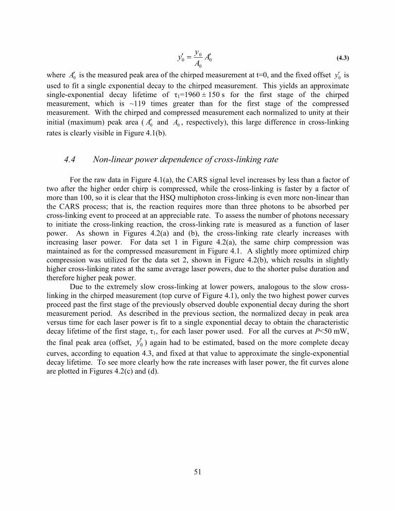
51
0
0
00 A
A
yy (4.3)
where 0A is the measured peak area of the chirped measurement at t=0, and the fixed offset 0y is
used to fit a single exponential decay to the chirped measurement. This yields an approximate
single-exponential decay lifetime of τ1=1960 ± 150 s for the first stage of the chirped
measurement, which is ~119 times greater than for the first stage of the compressed
measurement. With the chirped and compressed measurement each normalized to unity at their
initial (maximum) peak area ( 0A and 0A , respectively), this large difference in cross-linking
rates is clearly visible in Figure 4.1(b).
4.4 Non-linear power dependence of cross-linking rate
For the raw data in Figure 4.1(a), the CARS signal level increases by less than a factor of
two after the higher order chirp is compressed, while the cross-linking is faster by a factor of
more than 100, so it is clear that the HSQ multiphoton cross-linking is even more non-linear than
the CARS process; that is, the reaction requires more than three photons to be absorbed per
cross-linking event to proceed at an appreciable rate. To assess the number of photons necessary
to initiate the cross-linking reaction, the cross-linking rate is measured as a function of laser
power. As shown in Figures 4.2(a) and (b), the cross-linking rate clearly increases with
increasing laser power. For data set 1 in Figure 4.2(a), the same chirp compression was
maintained as for the compressed measurement in Figure 4.1. A slightly more optimized chirp
compression was utilized for the data set 2, shown in Figure 4.2(b), which results in slightly
higher cross-linking rates at the same average laser powers, due to the shorter pulse duration and
therefore higher peak power.
Due to the extremely slow cross-linking at lower powers, analogous to the slow cross-
linking in the chirped measurement (top curve of Figure 4.1), only the two highest power curves
proceed past the first stage of the previously observed double exponential decay during the short
measurement period. As described in the previous section, the normalized decay in peak area
versus time for each laser power is fit to a single exponential decay to obtain the characteristic
decay lifetime of the first stage, τ1, for each laser power used. For all the curves at P<50 mW,
the final peak area (offset, 0y ) again had to be estimated, based on the more complete decay
curves, according to equation 4.3, and fixed at that value to approximate the single-exponential
decay lifetime. To see more clearly how the rate increases with laser power, the fit curves alone
are plotted in Figures 4.2(c) and (d).
52
Figure 4.2 Normalized decay in the peak area for the cage-like HSQ band at 562 cm
-1 at different laser
powers for (a) data set 1, with slight chirp, and (b) data set 2, with optimal chirp compression. The
normalized peak area is equivalent to the relative degree of HSQ cross-linking (Eq. 4.7). A strong increase in
cross-linking rate is observed with increasing laser power in both set 1 and set 2. For clarity, single
exponential decay fit curves are shown alone in (c) for data set 1 and (d) for data set 2. The better
compression in set 2 results in slightly higher peak power and therefore slightly higher cross-linking rates at
the same average powers.
HSQ cross-linking always involves a decrease in linkages in exchange for more
, and depending on the specific reaction steps, it is possible that other reactants are also
consumed (such as O2 or H2O), and gaseous products released (such as SiH4, H2 or H2O),
explained in more detail in the following section (section 4.5). Regardless of the specific
reaction pathway, it is clear that for pulsed 800 nm excitation, a single cross-linking event is only
initiated when multiphoton absorption effectively “activates” a reactive site within the solid HSQ
film. A simplified, net HSQ cross-linking reaction for a single cross-linking event can be
expressed very generally as:
HSQcage + nPhotons HSQ*cage HSQnetwork (4.4)
where HSQcage refers to a reactive site in the as-spun film, capable of forming a cross-link
between “cage-like” species containing H, Si and O. HSQ*cage is the (short-lived) activated
reactive site, prior to cross-linking, possibly including a neutral excited state complex, broken
bonds, and ions or radicals. HSQnetwork refers to the “network-like” products of the single cross-
linking reaction, whether only partially cross-linked (still contain H atoms) or cross-linked to the
maximum extent possible, i.e. SiO4/2. The photo-activated reactive site in HSQ is analogous to a
53
photoinitiator molecule utilized in UV curing of traditional polymers,128
and first order kinetics
are expected if the rate of the photochemical reaction depends on the probability of
photoabsorption by this reactive site. The following laser power-dependent rate law is expected:
n
cage
cagePHSQk
dt
HSQd][
][1 (4.5)
where [HSQcage] is the total concentration of reactive cage-like species, t is exposure time in
seconds, P is the laser power in milliwatts (mW), n is the number of photons required to convert
each cage-like HSQ site to a network-like site, and k1 is a first order (or pseudo-first-order) rate
constant with units of mW-n
s-1
. Solving for the concentration of cage-like species versus time:
tPk
PcagePtcage
n
eHSQHSQ 1
,0, ][][
(4.6)
where PcageHSQ ,0][ and PtcageHSQ ,][ are the concentration of cage-like HSQ species present
initially (t=0) and after exposure time t.
In these CARS measurements, the concentration versus time is not measured directly, but
rather the integrated area of the 562 cm-1
CARS peak from the cage-like OSiO bend, At, versus
exposure time at constant power in the focused near IR beam. The CARS peak intensity varies
linearly with sample concentration, so the normalized peak area, At,norm, of the OSiO bend at
562 cm-1
after exposure time t at constant laser power P is directly proportional to the relative
concentration of cage-like HSQ bonds remaining after exposure, and thus the relative degree of
cross-linking which has occurred :
Pcage
Ptcage
normtHSQ
HSQA
,0
,
,][
][ . (4.7)
Inserting this into equation 4.6 gives:
tPk
normt
n
eA 1
,
. (4.8)
Thus, equation 4.9 is equivalent to the single exponential decay fit (Eq. 4.1) with 00 y . At the
characteristic initial decay lifetime, τ1, 1/e of the amplitude remains:
11
1
1,
nPk
norm ee
A
, (4.9)
and taking the natural log gives:
nPke
11
1ln
(4.10)
revealing the equality:
nPk1
1
1 . (4.11)
The initial decay lifetime (τ1) values are plotted (with error bars) versus average laser power
(measured before the microscope) in Figure 4.3(a). The uncertainty in the lifetimes,
incorporating both normalization uncertainty and noise, is approximately ±25% in set 1 and
±10% for set 2.
The rate constant k1 is unknown, so to derive the average number of photons, n, required
to initiate a single cross-linking event, the decay lifetime is compared for the various laser
54
powers. Taking the natural log of both sides of equation 4.11 and rearranging results in the
form:
)ln()ln()ln( 11 Pnk . (4.12)
Thus, a plot of –ln(τ1) versus ln(P) is linear, with slope n and y-intercept ln(k1), as shown in
Figure 4.3(b). A change in slope occurs at approximately 44 mW and 45.1 mW average power
for data set 1 and set 2, respectively, suggesting that a different cross-linking mechanism occurs
at lower powers. This is consistent with previously published works which show an average
power “threshold” for multiphoton ablation of positive tone resists.59
Here, the position of the
threshold is defined to maximize the agreement of the linear fits with the individual data points,
but the transition between these two regimes may not actually be well defined and instead exhibit
a cross-over region of average powers in which both mechanisms are occurring to some extent.
The n and k1 values for each of the data sets and the average values are summarized in Table 4.1.

55
Figure 4.3 HSQ cross-linking lifetime versus laser power. (a) Full range of measurements, inset is zoomed in
to high powers only, and error bars are encompassed by size of data markers where not visible. (b) Natural
log form of data following Eq. 4.12, error bars not shown. Best fit lines reveal a threshold for cross-linking
above which an average of ~6±1 photons is required per cross-linking event.

56
Data set Threshold
Above threshold Below Threshold
n
(# of photons) k1
(mW-n
s-1
) n
(# of photons) k1
(mW-n
s-1
)
1 ~45 mW 5.3 ± 0.8 8.4±1.0x10¹²
9.0 ± 1.4 3.5±0.4x10¹⁸
2 ~44 mW 6.4 ± 0.6 2.3±0.2x10¹³
10.9 ± 2.8 8.6±1.9x10²¹
Average n/a 5.9 ± 1.0 n/a 10.0 ± 3.1 n/a Table 4.1 Summary of fit parameters based on Figure 4.3(b) and equation 4.12.
The non-linearity of the lifetime versus laser power for the different data sets agrees to
within experimental uncertainty, suggesting that an average absorption of 6 ± 1 photons at a
wavelength of ~800 nm is required to initiate the cross-linking process in the higher power
regime, whereas at powers below the threshold an average of 10 ± 3 photons is required. The
large error bar below threshold is due to the larger uncertainty in the offset 0y for the low power
curves, as well as worse signal-to-noise in low-power CARS spectra due to lower signal levels.
For the low power curves, it is possible that the offset, 0y , is actually lower than estimated, due
to a greater degree of cross-linking at t=∞ with the slower reaction rate; this has been shown
previously in UV cured polymers with photoinitiators, where a faster initial cross-linking rate
limits the total degree of cross-linking by locking in the network structure and stopping the
reaction at an earlier stage, with more unreacted monomers remaining.128
At first it seems
counter-intuitive that more photons are required per cross-linking event in the low average power
regime, where the cross-linking rate is very low. However, it is possible that a completely
different, photothermal mechanism is responsible for the cross-linking in the low power regime,
where the energy of the ~10 photons is deposited over many different bonds, while the high-
power regime involves direct photo-induced bond breaking. Understanding the non-linearity
requires an in-depth look at the possible cross-linking mechanisms, provided in the following
section.
The cross-linking rate constant k1 is higher for data set 2 than for data set 1 because better
chirp compression, and therefore higher peak power density, was utilized for set 2 at the same
average powers. This higher rate constant (k1) also results in the lower threshold power for set 2,
as shown in Figure 4.3(b) and Table 4.1. This is consistent with the conclusion previously
reported by Ibrahim et al. regarding multiphoton photolithography of positive-tone resists, where
the kτ values of various materials were compared; a lower kτ resulted in a higher power threshold
for multiphoton lithography and etching.59
Also noted by Ibrahim et al., the multiphoton rate constant is very sensitive to small
fluctuations in the microscope focus conditions, leading to large uncertainty on the order of
kτ±100%. Variations in focus are analogous to variations in chirp, as either an increase in the
size of the focal spot or an increase in the pulse duration will decrease the power density at the
focus in the sample. For example, in the experiments presented here, an increase in the focal
spot diameter from 400 nm to just 450 nm reduces the peak power density significantly, by
~21% (calculated). Likewise, for a fixed spot size of 400 nm at constant average power, a very
small amount of chirp is sufficient to increase the pulse duration from 38 to 48 fs, which also
reduces the peak power density by ~21% (calculated). Therefore, more realistic error bars on the
k1 values from the linear fit may be on the same order of magnitude as the values themselves.
This sensitivity to peak power explains the fluctuations observed between measurements
in the present study. As noted previously, small changes in chirp and focusing likely occur over

57
time due to variations with sample position, beam pointing, and temperature of optics in the
SLM and laser cavity. For the data in set 1, the 67 mW points (chirped and compressed) were
acquired first, and the remaining curves were then measured sequentially (in order) from low to
high power. Thus, any small drift in the system may lead to systematic error and slightly alter
the slope of the fit lines for data set 1 in Figure 4.3(b). However, for data set 2, the measurement
of low and high power kinetics curves was alternated in a random order to randomize the effects
of long term drift. This is evident in Figure 4.3(b) as larger scatter in the points for data set 2.
Table 4.2 summarizes the average laser powers and measured lifetimes. A single
exponential lifetime is used for comparing lifetimes, but double exponential fits can be
approximated for a few of the highest power curves. The estimated lifetimes from the double
exponential decay, 1 and 2 , are also reported in Table 4.2 when possible. However, due to the
short measurement time, these double exponential decay lifetimes are generally underestimated,
and they are not accessible for the lower power measurements. In future experiments, it is
desirable to improve the long-term stability of the system to measure the decay curve at each
power for a much longer acquisition time, such that the τ1 lifetimes can be assessed with more
certainty, and the τ2 lifetimes can be used to determine the non-linearity of the second stage, as
well.

58
Power, mW
(± 0.2 mW)
Single exponential fit
decay lifetime,
τ1, seconds
Double exponential fit
decay lifetimes, seconds
1 τ2
67, CHIRPED 1960 ± 150
DATA SET 1, Nearly Optimized Chirp Compression
67, COMPRESSED 16.5 ± 2.5 7.6 ± 3.6 33.7 ± 6.3
65.0 35.0 ± 5.0 22.2 ± 4.8 350 ± 350
60.0 43.1 ± 3.0
55.9 66.8 ± 3.8
51.1 86.6 ± 5.0
48.0 130.5 ± 10.2
45.1 361 ± 90
43.1 1009.3 ± 218
39.0 1509.4 ± 271
36.4 2531.8 ± 395
34.5 5872.9 ± 377
DATA SET 2, Optimized Chirp Compression 60.2 18.2 ± 1.1 5.6 ± 3.6 25.6 ± 7.2
58.4 19.7 ± 1.8 15.3 ± 2.6 163 ± 163
57.3 16.6 ± 0.8
54.6 29.8 ± 1.6
54 46.5 ± 3.4
53.2 27.2 ± 0.7
51.8 37.6 ± 4.9
49.9 49.8 ± 3.4
49.8 63.7 ± 4.6
49.8 54.7 ± 4.0
49 53.6 ± 6.5
48.8 81.1 ± 10.3
47.2 64.4 ± 4.4
45.3 106.4 ± 3.1
44 114.9 ± 3.1
41.7 225 ± 13
39.7 397 ± 21
39.7 284.5 ± 15
37.8 659 ± 38
Table 4.2 Summary of all measured power values and time constants for near IR HSQ cross-linking.
4.5 A closer look at potential cross-linking mechanisms and reaction
order
As mentioned previously, the high degree of non-linearity for MAP of HSQ is expected
based on previous reports of HSQ cross-linking only at exposure wavelengths ≤ 157 nm,
corresponding to a photon energy of 7.90 eV. By comparison, the laser spectrum used in this
study covers the range from 740 nm to 860 nm, or photon energies from 1.44 eV to 1.67 eV.
The non-linearity of 6±1 photons for the pulsed NIR-induced cross-linking “above threshold”

59
corresponds to 9.4 ± 2.2 eV, the lower limit of which is near the same energy as a single 157 nm
photon. This is sufficient to break approximately one SiO bond (~8.94 eV) or two SiH bonds
(~4.08 eV each), with any excess energy possibly going into thermal excitation. Notably, a
single 157 nm photon would be sufficient to break two bonds only if the bond
dissociation energy in HSQ is ~3.95 eV, just slightly lower than the previously reported value of
~4.08 eV (under unknown conditions).43
The exact and bond strengths in the HSQ
thin film probably do vary somewhat from reported literature values, based on specific sample
characteristics. More than one explanation is possible for the high degree of non-linearity in
each stage, and several hypotheses are explored here.
Two previously proposed mechanisms, shown below, depend upon the cleavage of two
bonds on adjacent Si atoms to initiate a single cross-linking event. The e-beam
mechanism is expected to involve direct bond cleavage followed by the uptake of water,
leading to one added oxygen atom per cross-linking event:37
(4.13)
via the following reaction steps:
(4.14)
where ΔE is energy deposited via e-beam. The fate of the H radicals has not been reported, but it
is possible that they form H2, and/or react with additional Si or O atoms in the HSQ network. A
very similar mechanism has been proposed for thermally-induced HSQ cross-linking at high
temperatures (>400 °C), which also involves cleavage and the uptake of oxygen atoms
from O2 instead of water:129
(4.15)
where ΔE is thermal energy. Although two bonds must be broken per cross-linking event
in either case, the reaction depends upon the two species being in close proximity, so it could
still be first order in the number of properly oriented and juxtaposed reactive sites. The initial
rate would not likely be limited by the number of individual bonds present, as they are
greatly in excess. Thus, the ~6 photon dependence and possibly first order reaction kinetics
(above the threshold) could indicate the breaking of two adjacent bonds for each cross-
linking event.
Perhaps because the bond is weaker, and the onset of photolytic conversion is
157 nm, no previous mechanisms have mentioned the direct cleavage of an bond to initiate
cross-linking, but the ~9.4 eV energy dependence revealed here is just slightly higher than the
expected bond strength. Thus, another possible photolytic pathway could be cleavage of a
single bond, essentially resulting in a cage opening, followed by the bond redistribution
(exchange) mechanism shown in Figure 4.4, where “R” represents the remaining cage-like or
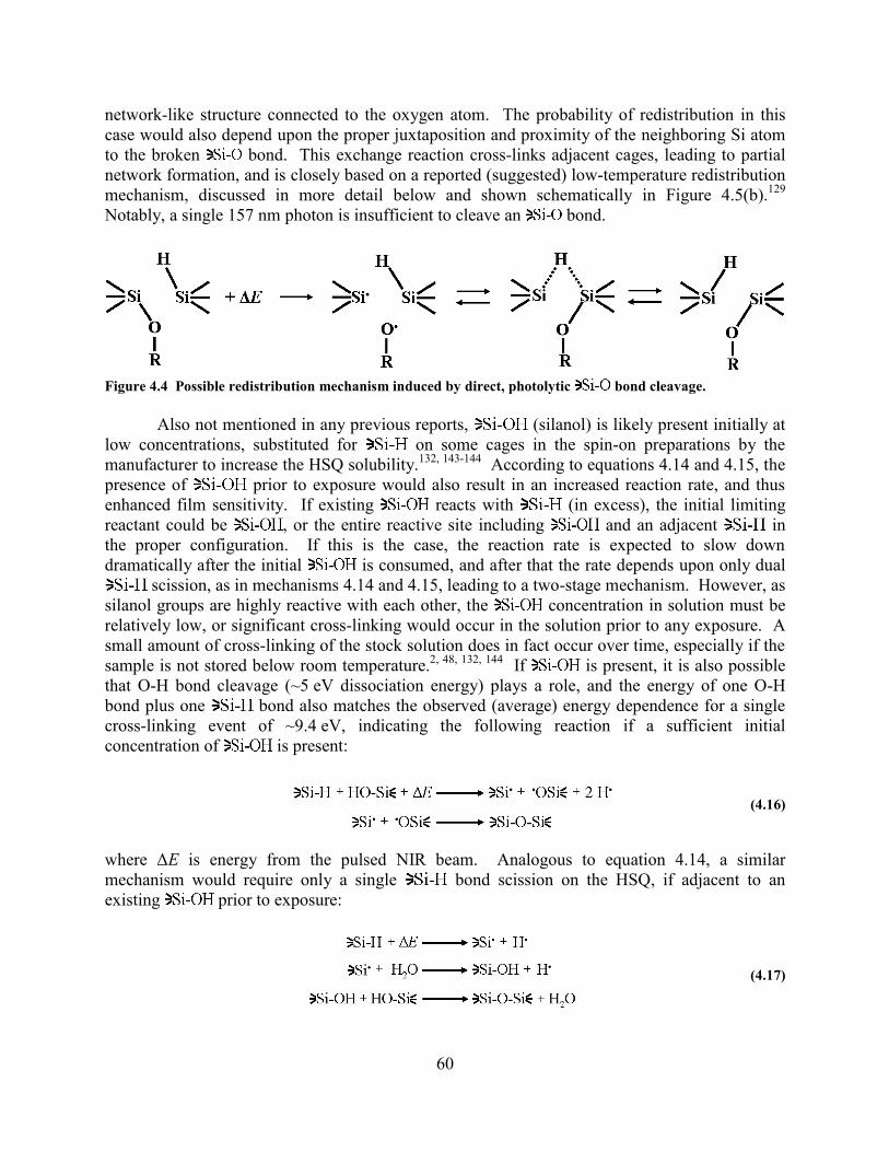
60
network-like structure connected to the oxygen atom. The probability of redistribution in this
case would also depend upon the proper juxtaposition and proximity of the neighboring Si atom
to the broken bond. This exchange reaction cross-links adjacent cages, leading to partial
network formation, and is closely based on a reported (suggested) low-temperature redistribution
mechanism, discussed in more detail below and shown schematically in Figure 4.5(b).129
Notably, a single 157 nm photon is insufficient to cleave an bond.
Figure 4.4 Possible redistribution mechanism induced by direct, photolytic bond cleavage.
Also not mentioned in any previous reports, (silanol) is likely present initially at
low concentrations, substituted for on some cages in the spin-on preparations by the
manufacturer to increase the HSQ solubility.132, 143-144
According to equations 4.14 and 4.15, the
presence of prior to exposure would also result in an increased reaction rate, and thus
enhanced film sensitivity. If existing reacts with (in excess), the initial limiting
reactant could be , or the entire reactive site including and an adjacent in
the proper configuration. If this is the case, the reaction rate is expected to slow down
dramatically after the initial is consumed, and after that the rate depends upon only dual
scission, as in mechanisms 4.14 and 4.15, leading to a two-stage mechanism. However, as
silanol groups are highly reactive with each other, the concentration in solution must be
relatively low, or significant cross-linking would occur in the solution prior to any exposure. A
small amount of cross-linking of the stock solution does in fact occur over time, especially if the
sample is not stored below room temperature.2, 48, 132, 144
If is present, it is also possible
that O-H bond cleavage (~5 eV dissociation energy) plays a role, and the energy of one O-H
bond plus one bond also matches the observed (average) energy dependence for a single
cross-linking event of ~9.4 eV, indicating the following reaction if a sufficient initial
concentration of is present:
(4.16)
where ΔE is energy from the pulsed NIR beam. Analogous to equation 4.14, a similar
mechanism would require only a single bond scission on the HSQ, if adjacent to an
existing prior to exposure:
(4.17)
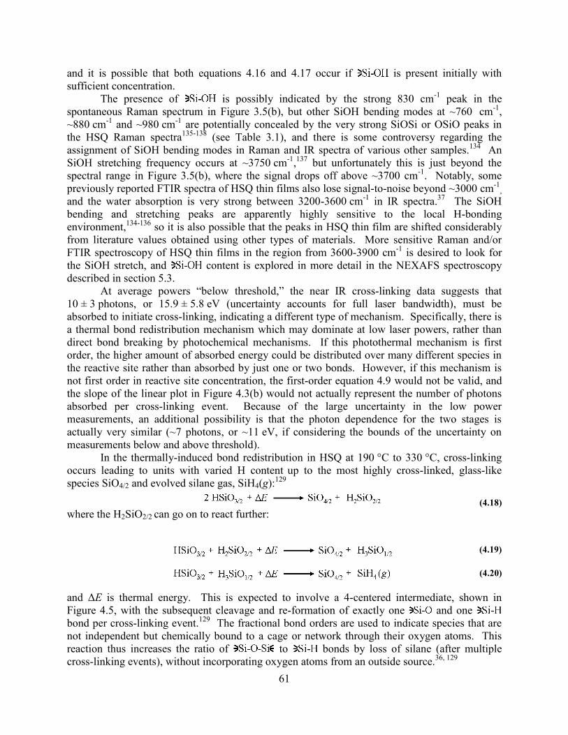
61
and it is possible that both equations 4.16 and 4.17 occur if is present initially with
sufficient concentration.
The presence of is possibly indicated by the strong 830 cm-1
peak in the
spontaneous Raman spectrum in Figure 3.5(b), but other SiOH bending modes at ~760 cm1
,
~880 cm1
and ~980 cm1
are potentially concealed by the very strong SiOSi or OSiO peaks in
the HSQ Raman spectra135-138
(see Table 3.1), and there is some controversy regarding the
assignment of SiOH bending modes in Raman and IR spectra of various other samples.134
An
SiOH stretching frequency occurs at ~3750 cm1
,137
but unfortunately this is just beyond the
spectral range in Figure 3.5(b), where the signal drops off above ~3700 cm-1
. Notably, some
previously reported FTIR spectra of HSQ thin films also lose signal-to-noise beyond ~3000 cm-1
,
and the water absorption is very strong between 3200-3600 cm-1
in IR spectra.37
The SiOH
bending and stretching peaks are apparently highly sensitive to the local H-bonding
environment,134-136
so it is also possible that the peaks in HSQ thin film are shifted considerably
from literature values obtained using other types of materials. More sensitive Raman and/or
FTIR spectroscopy of HSQ thin films in the region from 3600-3900 cm-1
is desired to look for
the SiOH stretch, and content is explored in more detail in the NEXAFS spectroscopy
described in section 5.3.
At average powers “below threshold,” the near IR cross-linking data suggests that
10 ± 3 photons, or 15.9 ± 5.8 eV (uncertainty accounts for full laser bandwidth), must be
absorbed to initiate cross-linking, indicating a different type of mechanism. Specifically, there is
a thermal bond redistribution mechanism which may dominate at low laser powers, rather than
direct bond breaking by photochemical mechanisms. If this photothermal mechanism is first
order, the higher amount of absorbed energy could be distributed over many different species in
the reactive site rather than absorbed by just one or two bonds. However, if this mechanism is
not first order in reactive site concentration, the first-order equation 4.9 would not be valid, and
the slope of the linear plot in Figure 4.3(b) would not actually represent the number of photons
absorbed per cross-linking event. Because of the large uncertainty in the low power
measurements, an additional possibility is that the photon dependence for the two stages is
actually very similar (~7 photons, or ~11 eV, if considering the bounds of the uncertainty on
measurements below and above threshold).
In the thermally-induced bond redistribution in HSQ at 190 °C to 330 °C, cross-linking
occurs leading to units with varied H content up to the most highly cross-linked, glass-like
species SiO4/2 and evolved silane gas, SiH4(g):129
(4.18)
where the H2SiO2/2 can go on to react further:
(4.19)
(4.20)
and ΔE is thermal energy. This is expected to involve a 4-centered intermediate, shown in
Figure 4.5, with the subsequent cleavage and re-formation of exactly one and one
bond per cross-linking event.129
The fractional bond orders are used to indicate species that are
not independent but chemically bound to a cage or network through their oxygen atoms. This
reaction thus increases the ratio of to bonds by loss of silane (after multiple
cross-linking events), without incorporating oxygen atoms from an outside source.36, 129

62
Figure 4.5 Schematic representation of the proposed 4-centered intermediate of the redistribution reaction,
shown (a) in the plane of the page, where R represents any interconnected species,129
and (b) in a slightly
more realistic geometry, which shows possible interconnected species for the first cross-linking event.
All of the previously proposed reaction mechanisms are summarized schematically in
Figure 4.6. One thing they have in common is that two species must come together to form a
cross-link. However, to understand the reaction order for cross-linking of HSQ, as opposed to
traditional chain-like organic polymers, it is challenging to define independent reactive species.
For example, the HSiO3/2 or H2SiO2/2 moieties are not independent but share all of their oxygen
atoms with adjacent Si atoms. As stated previously, for kinetics measurements in the solid HSQ
film, where the mobility of individual species or even independent monomer cages is severely
restricted, it makes more sense to consider an entire reactive site, including all adjacent atoms, as
a single reactant. This is equivalent to saying that in order for two species to cross-link within
the solid, they must be adjacent and in approximately the proper geometry prior to exposure. For
example, in the redistribution reaction shown in Figure 4.5, all of the atoms directly involved in
the 4-centered intermediate and their nearest neighbors can be considered collectively as the
reactive site. The cross-linking will not occur unless all of these species are present locally and
oriented with the proper geometry prior to exposure in the as-spun film, and thus the reaction
rate could be limited by the concentration of these specific reactive sites within the focal volume.
For the above threshold cross-linking, at least, this is supported by the apparently first order
kinetics, which suggest that the rate is not limited by two or more individual species coming
together, but rather by the concentration of a single, reactive unit. Other photoinduced cross-
linking reactions, which involve photoinitiator molecules as the absorbing species, have also
been observed to follow apparent first order kinetics.128
However, it is important to note that the
order of the observed kinetics may only indicate the order of the photolytic activation step, and
not necessarily reveal the overall order of the reaction.
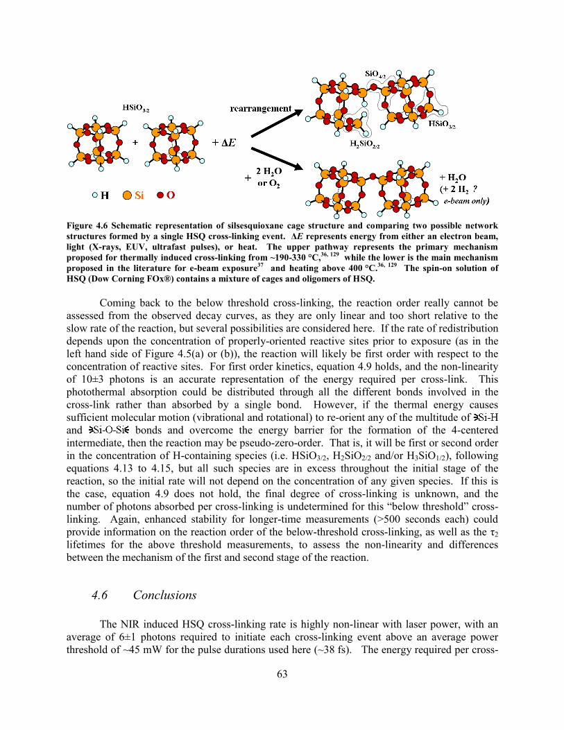
63
Figure 4.6 Schematic representation of silsesquioxane cage structure and comparing two possible network
structures formed by a single HSQ cross-linking event. ΔE represents energy from either an electron beam,
light (Xrays, EUV, ultrafast pulses), or heat. The upper pathway represents the primary mechanism
proposed for thermally induced cross-linking from ~190-330 °C,36, 129
while the lower is the main mechanism
proposed in the literature for e-beam exposure37
and heating above 400 °C.36, 129
The spin-on solution of
HSQ (Dow Corning FOx®) contains a mixture of cages and oligomers of HSQ.
Coming back to the below threshold cross-linking, the reaction order really cannot be
assessed from the observed decay curves, as they are only linear and too short relative to the
slow rate of the reaction, but several possibilities are considered here. If the rate of redistribution
depends upon the concentration of properly-oriented reactive sites prior to exposure (as in the
left hand side of Figure 4.5(a) or (b)), the reaction will likely be first order with respect to the
concentration of reactive sites. For first order kinetics, equation 4.9 holds, and the non-linearity
of 10±3 photons is an accurate representation of the energy required per cross-link. This
photothermal absorption could be distributed through all the different bonds involved in the
cross-link rather than absorbed by a single bond. However, if the thermal energy causes
sufficient molecular motion (vibrational and rotational) to re-orient any of the multitude of
and bonds and overcome the energy barrier for the formation of the 4-centered
intermediate, then the reaction may be pseudo-zero-order. That is, it will be first or second order
in the concentration of H-containing species (i.e. HSiO3/2, H2SiO2/2 and/or H3SiO1/2), following
equations 4.13 to 4.15, but all such species are in excess throughout the initial stage of the
reaction, so the initial rate will not depend on the concentration of any given species. If this is
the case, equation 4.9 does not hold, the final degree of cross-linking is unknown, and the
number of photons absorbed per cross-linking is undetermined for this “below threshold” cross-
linking. Again, enhanced stability for longer-time measurements (>500 seconds each) could
provide information on the reaction order of the below-threshold cross-linking, as well as the τ2
lifetimes for the above threshold measurements, to assess the non-linearity and differences
between the mechanism of the first and second stage of the reaction.
4.6 Conclusions
The NIR induced HSQ cross-linking rate is highly non-linear with laser power, with an
average of 6±1 photons required to initiate each cross-linking event above an average power
threshold of ~45 mW for the pulse durations used here (~38 fs). The energy required per cross-
64
link is consistent with previously proposed reaction mechanisms involving direct bond
cleavage by ebeam or heat, but additional possibilities are presented involving existing
(silanol) groups in the as-spun thin films or bond scission. Further studies are required to
assess the initial concentration of in the films, as the spontaneous Raman spectra (Chapter
3) are inconclusive, but X-ray spectra presented in Chapter 5 do indicate the presence of .
First-order kinetics for photochemical conversion are suggested by the shape of the decay curves,
and based on literature reports of UV curing in traditional polymers.128
The two-stage nature of
the reaction with exposure time is possibly due to the loss of groups with cross-linking,
the increasing rigidity of the cross-linked network, and/or the consumption of easily cross-linked
reactive sites.
Below the observed threshold of ~45 mW, slower cross-linking is observed with a
slightly different power dependence, possibly by a photothermal bond redistribution mechanism.
Assuming first order kinetics below the threshold, this suggests an average absorption of 10±3
photons per cross-link. However, while the rate-limiting step in the photolytic conversion above
the threshold appears to be first order, the results of the present study cannot confirm that the
kinetics are also first order below the threshold.
The cross-linking rate is highly dependent on the peak power of the laser pulses, and thus
the degree of chirp (spectral phase). Compression of the higher order chirp with the SLM (3rd
and 4th
order spectral phase) results in a >100 fold increase in the HSQ cross-linking rate for the
same average laser power, but just a two-fold increase in DQSI-CARS signal intensity. Thus, by
utilizing chirped pulses and fast scan rates, DQSI-CARS should be capable of imaging HSQ and
other sensitive polymer photoresists without inducing significant damage by using damage-
mitigation techniques such as fast scan rates, similar to the STXM techniques detailed in Chapter
5. On the other hand, higher average and/or peak laser power can provide rapid cross-linking for
direct-write NIR MAP lithography. With the high order non-linearity of the cross-linking
process, this multiphoton lithography may provide an important new tool for microfabrication in
HSQ and related materials.
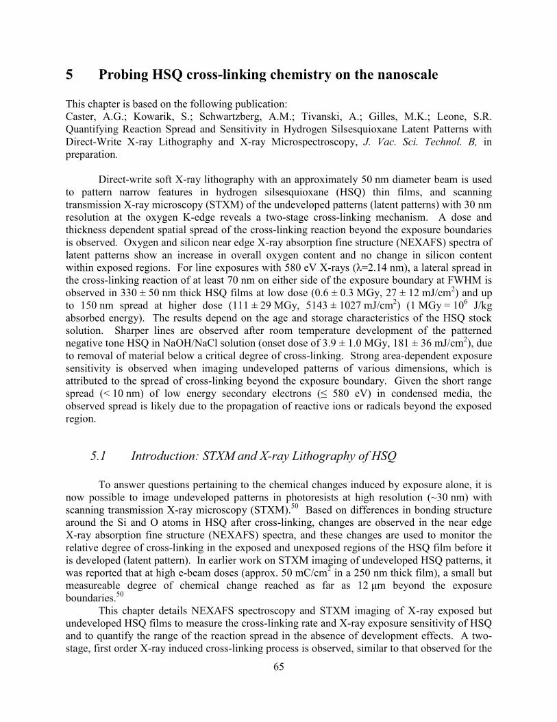
65
5 Probing HSQ cross-linking chemistry on the nanoscale
This chapter is based on the following publication:
Caster, A.G.; Kowarik, S.; Schwartzberg, A.M.; Tivanski, A.; Gilles, M.K.; Leone, S.R.
Quantifying Reaction Spread and Sensitivity in Hydrogen Silsesquioxane Latent Patterns with
Direct-Write X-ray Lithography and X-ray Microspectroscopy, J. Vac. Sci. Technol. B, in
preparation.
Direct-write soft X-ray lithography with an approximately 50 nm diameter beam is used
to pattern narrow features in hydrogen silsesquioxane (HSQ) thin films, and scanning
transmission X-ray microscopy (STXM) of the undeveloped patterns (latent patterns) with 30 nm
resolution at the oxygen K-edge reveals a two-stage cross-linking mechanism. A dose and
thickness dependent spatial spread of the cross-linking reaction beyond the exposure boundaries
is observed. Oxygen and silicon near edge X-ray absorption fine structure (NEXAFS) spectra of
latent patterns show an increase in overall oxygen content and no change in silicon content
within exposed regions. For line exposures with 580 eV X-rays (λ=2.14 nm), a lateral spread in
the cross-linking reaction of at least 70 nm on either side of the exposure boundary at FWHM is
observed in 330 ± 50 nm thick HSQ films at low dose (0.6 ± 0.3 MGy, 27 ± 12 mJ/cm2) and up
to 150 nm spread at higher dose (111 ± 29 MGy, 5143 ± 1027 mJ/cm2) (1 MGy = 106 J/kg
absorbed energy). The results depend on the age and storage characteristics of the HSQ stock
solution. Sharper lines are observed after room temperature development of the patterned
negative tone HSQ in NaOH/NaCl solution (onset dose of 3.9 ± 1.0 MGy, 181 ± 36 mJ/cm2), due
to removal of material below a critical degree of cross-linking. Strong area-dependent exposure
sensitivity is observed when imaging undeveloped patterns of various dimensions, which is
attributed to the spread of cross-linking beyond the exposure boundary. Given the short range
spread (< 10 nm) of low energy secondary electrons (≤ 580 eV) in condensed media, the
observed spread is likely due to the propagation of reactive ions or radicals beyond the exposed
region.
5.1 Introduction: STXM and X-ray Lithography of HSQ
To answer questions pertaining to the chemical changes induced by exposure alone, it is
now possible to image undeveloped patterns in photoresists at high resolution (~30 nm) with
scanning transmission X-ray microscopy (STXM).50
Based on differences in bonding structure
around the Si and O atoms in HSQ after cross-linking, changes are observed in the near edge
Xray absorption fine structure (NEXAFS) spectra, and these changes are used to monitor the
relative degree of cross-linking in the exposed and unexposed regions of the HSQ film before it
is developed (latent pattern). In earlier work on STXM imaging of undeveloped HSQ patterns, it
was reported that at high e-beam doses (approx. 50 mC/cm2 in a 250 nm thick film), a small but
measureable degree of chemical change reached as far as 12 μm beyond the exposure
boundaries.50
This chapter details NEXAFS spectroscopy and STXM imaging of X-ray exposed but
undeveloped HSQ films to measure the cross-linking rate and X-ray exposure sensitivity of HSQ
and to quantify the range of the reaction spread in the absence of development effects. A two-
stage, first order X-ray induced cross-linking process is observed, similar to that observed for the

66
near IR multiphoton cross-linking, resulting in the incorporation of additional oxygen atoms into
the cross-linked regions. A FWHM spread of the cross-linking reaction is observed to be greater
than 70 nm, depending on the film thickness and Xray dose, and the reaction spread is shown to
cause proximity effects leading to significant area-dependent sensitivity. Comparing the same
patterns before and after development in solution, the NaOH/NaCl developer washes away the
partially cross-linked material evident in the undeveloped HSQ images, as anticipated, including
cross-linking caused by reaction spread.
5.2 Sample Preparation and experimental setup
HSQ thin films from 100-500 nm thick are prepared on 100 nm thick silicon nitride
substrates. For patterning, spectroscopy, and imaging, the sample patterns are written and
analyzed in the 5.3.2 STXM described in section 2.4.120
For X-ray lithography, Xrays at either
536 eV or 580 eV are tightly focused on the film surface to an approximately 50 nm diameter
spot (FWHM), and the sample is raster scanned through the stationary X-ray beam in a pre-
defined pattern. NEXAFS spectra of the films are measured across the oxygen atom K-edge
(520 eV to 700 eV) to measure changes in the chemical structure around the oxygen atoms
before and after X-ray exposure. Within 5 minutes after patterning, images of exposed patterns
are obtained with ~30 nm spatial resolution without significant further sample damage by
reducing the photon flux and scanning the sample more rapidly through the X-ray beam at a
fixed energy (536 eV, oxygen K-edge). Images are analyzed to measure the relative degree of
chemical change for each exposure dose and the lateral spread of the X-ray induced chemistry.
Additionally, NEXAFS spectra at the silicon atom K-edge (1825 eV to 1880 eV) are measured
before and after exposure at the STXM on beamline 11.0.2 of the ALS.145
To prepare HSQ films, 5 μL of Dow Corning XR-1541 (6% HSQ in methyl isobutyl
ketone, for 100 nm thick films), Dow Corning FOx-15® (15-40% HSQ in methyl isobutyl
ketone, for 300-400 nm thick films), or Dow Corning FOx-25® (15-40% HSQ in toluene,
octamethyltrisiloxane and hexamethyldisiloxane, for 500 nm thick films) are spin-cast at 2000-
6000 RPM for 30 s onto a 100 nm thick silicon nitride (Si3N4) membrane substrate (Silson
Limited, shown in Figure 2.17). This thin silicon nitride has a high transmission in the X-ray
energy regions of interest. The transmitted spectrum and photon flux through a blank substrate
are measured periodically to record the background for all analyses. The reported results were
obtained using HSQ stock solutions stored continuously at -15 °C for up to 2.5 years prior to
film preparation. The results may vary if freshly synthesized HSQ material is utilized
immediately. Only those films noted as “pre-baked” are baked on a hot plate in air for 5 min at
150 °C to drive off excess solvent prior to exposure. As the HSQ films are smooth and
featureless, 100 nm gold nanoparticles are added on top of the film to enable sharp focusing of
the X-ray beam on the surface, a requirement for producing the sharpest lithographic features
and highest imaging resolution with the microscope. After placing a 1.5 L droplet of very
dilute nanoparticles on the surface, the films are dried and stored in air for 15 hours before being
placed under vacuum in the X-ray microscope sample chamber. The sample chamber is
evacuated to 0.2 Torr (~26.7 Pa) (sufficient to remove excess solvent in unbaked samples) then
backfilled with 300 Torr of He.
As detailed in section 2.4, the STXM at beamline 5.3.2 uses a 25 nm outer-diameter
Fresnel zone plate lens to focus synchrotron-generated soft X-rays on the HSQ thin films. The

67
monochromator is used to select the photon energy, and three sets of monochromator slits
control the photon flux and spatial resolution of the microscope (as shown in Table 2.2). In this
experiment, wider settings for the three slits (80 μm, 40 μm, and 40 μm) are used for lithography,
giving a photon flux on the order of 106 photons/s and ~50 nm beam diameter (FWHM), while
narrower slits (40 μm, 20 μm, and 20 μm) are used for imaging, reducing the photon flux by a
factor of ~4 and improving the spatial resolution to ~30 nm (Rayleigh limit, based on zone plate
outer diameter4). The depth of focus for these experiments (equation 2.39)
4 is ~1.0-1.2 μm, so
100 nm diameter gold particles are used to bring the beam focus to within ± 500 nm of the film
surface prior to all patterning and imaging, and thus the beam is tightly focused through the
entire film thickness (≤ 500 nm).
To obtain images, the X-ray transmission through the sample is measured at a fixed
photon energy as the sample is scanned through the beam. For NEXAFS spectra, the photon
energy is scanned across a range of values for each sample position of interest. For both imaging
and spectroscopy, the measured transmission is compared to transmission through a blank silicon
nitride membrane substrate and converted to optical density (OD) according to the natural log
form of Beer’s law (analogous to equation 2.34):
lEI
IOD )(ln
0
(5.1)
where I is the X-ray flux through the sample plus substrate and 0I is the incident photon flux
through the blank substrate. The OD is sensitive to the film thickness, l, density, ρ, and energy-
dependent mass absorption coefficient, μ(E). A minimum film thickness of ~300 nm is used to
achieve a high signal-to-noise ratio in STXM imaging of unexposed and exposed HSQ regions at
the oxygen K-edge. The contrast within each image, which will be related to the degree of cross
linking, is quantified by calculating the relative OD between the exposed and unexposed regions:
osedun
osedosedunosed
osedunosedI
I
I
I
I
IODODOD
exp
exp
0
exp
0
exp
expexp lnlnln (5.2)
For patterning, we assume the beam profile as shown in Figure 5.1(a), with an ~50 nm
FWHM, based on the imaging resolution, new and previously reported knife-edge
measurements.4, 146-148
Single-pass lines are produced by stepping the sample through the beam
with a fixed step size of 50 nm or 200 nm, as shown in Figure 5.1(b) and Figure 5.1(c), with a
per point exposure time (dwell time) ranging from 2 ms to 7.7 seconds. Longer dwell times or
smaller step sizes result in a higher deposited dose and thus a greater degree of cross-linking.
Wide features are patterned by exposing n adjacent single-pass lines, with the space between
lines equivalent to the step size (50 nm or 200 nm), as shown in Figure 5.1(d). The 50 nm step
size results in slight overlap between the exposed points, but the extensive reaction spread in
these films causes a high degree of cross-linking between exposed points even with 200 nm point
spacing, which is elucidated in later sections.
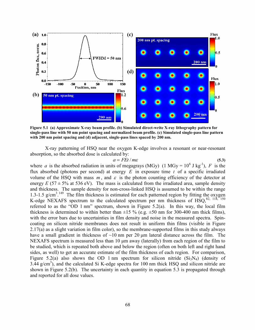
68
Figure 5.1 (a) Approximate X-ray beam profile. (b) Simulated direct-write X-ray lithography pattern for
single-pass line with 50 nm point spacing and normalized beam profile. (c) Simulated single-pass line pattern
with 200 nm point spacing and (d) adjacent, single-pass lines spaced by 200 nm.
X-ray patterning of HSQ near the oxygen K-edge involves a resonant or near-resonant
absorption, so the absorbed dose is calculated by:
mFEta / (5.3)
where a is the absorbed radiation in units of megagrays (MGy) (1 MGy = 106 J kg
-1), F is the
flux absorbed (photons per second) at energy E in exposure time t of a specific irradiated
volume of the HSQ with mass m , and is the photon counting efficiency of the detector at
energy E (57 ± 5% at 536 eV). The mass is calculated from the irradiated area, sample density
and thickness. The sample density for non-cross-linked HSQ is assumed to be within the range
1.3-1.5 g/cm3.149
The film thickness is estimated for each patterned region by fitting the oxygen
K-edge NEXAFS spectrum to the calculated spectrum per nm thickness of HSQ,82, 118, 150
referred to as the “OD 1 nm” spectrum, shown in Figure 5.2(a). In this way, the local film
thickness is determined to within better than ±15 % (e.g. ±50 nm for 300-400 nm thick films),
with the error bars due to uncertainties in film density and noise in the measured spectra. Spin-
coating on silicon nitride membranes does not result in uniform thin films (visible in Figure
2.17(a) as a slight variation in film color), so the membrane-supported films in this study always
have a small gradient in thickness of ~10 nm per 20 μm lateral distance across the film. The
NEXAFS spectrum is measured less than 10 μm away (laterally) from each region of the film to
be studied, which is repeated both above and below the region (often on both left and right hand
sides, as well) to get an accurate estimate of the film thickness of each region. For comparison,
Figure 5.2(a) also shows the OD 1 nm spectrum for silicon nitride (Si3N4) (density of
3.44 g/cm3), and the calculated Si K-edge spectra for 100 nm thick HSQ and silicon nitride are
shown in Figure 5.2(b). The uncertainty in each quantity in equation 5.3 is propagated through
and reported for all dose values.
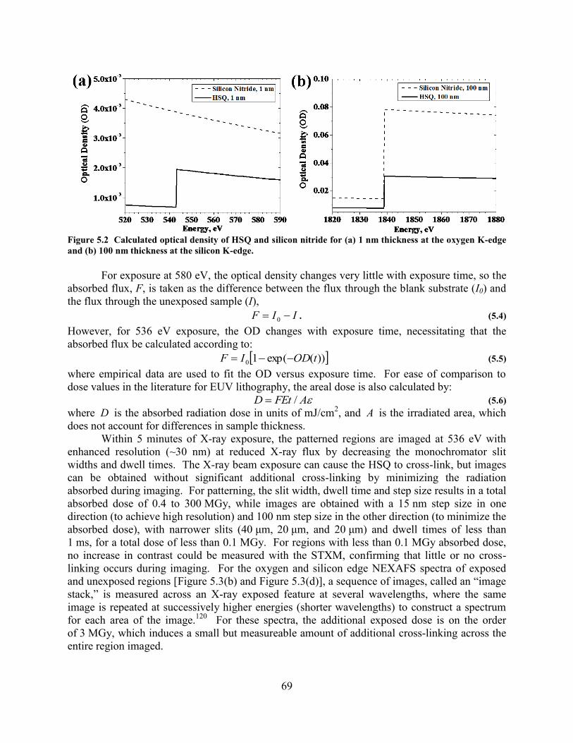
69
Figure 5.2 Calculated optical density of HSQ and silicon nitride for (a) 1 nm thickness at the oxygen K-edge
and (b) 100 nm thickness at the silicon K-edge.
For exposure at 580 eV, the optical density changes very little with exposure time, so the
absorbed flux, F, is taken as the difference between the flux through the blank substrate (I0) and
the flux through the unexposed sample (I),
IIF 0 . (5.4)
However, for 536 eV exposure, the OD changes with exposure time, necessitating that the
absorbed flux be calculated according to:
))(exp(10 tODIF (5.5)
where empirical data are used to fit the OD versus exposure time. For ease of comparison to
dose values in the literature for EUV lithography, the areal dose is also calculated by:
AFEtD / (5.6)
where D is the absorbed radiation dose in units of mJ/cm2, and A is the irradiated area, which
does not account for differences in sample thickness.
Within 5 minutes of X-ray exposure, the patterned regions are imaged at 536 eV with
enhanced resolution (~30 nm) at reduced X-ray flux by decreasing the monochromator slit
widths and dwell times. The X-ray beam exposure can cause the HSQ to cross-link, but images
can be obtained without significant additional cross-linking by minimizing the radiation
absorbed during imaging. For patterning, the slit width, dwell time and step size results in a total
absorbed dose of 0.4 to 300 MGy, while images are obtained with a 15 nm step size in one
direction (to achieve high resolution) and 100 nm step size in the other direction (to minimize the
absorbed dose), with narrower slits (40 μm, 20 μm, and 20 μm) and dwell times of less than
1 ms, for a total dose of less than 0.1 MGy. For regions with less than 0.1 MGy absorbed dose,
no increase in contrast could be measured with the STXM, confirming that little or no cross-
linking occurs during imaging. For the oxygen and silicon edge NEXAFS spectra of exposed
and unexposed regions [Figure 5.3(b) and Figure 5.3(d)], a sequence of images, called an “image
stack,” is measured across an X-ray exposed feature at several wavelengths, where the same
image is repeated at successively higher energies (shorter wavelengths) to construct a spectrum
for each area of the image.120
For these spectra, the additional exposed dose is on the order
of 3 MGy, which induces a small but measureable amount of additional cross-linking across the
entire region imaged.

70
After X-ray exposure and imaging, patterned films are developed for 4 minutes at room
temperature in a high contrast developer solution of 1 wt% NaOH and 4 wt% NaCl in Millipore
water to wash away the unexposed material.151
The developed patterns are subsequently imaged
with a field emission scanning electron microscope (SEM, JEOL JSM 6340F) and again with the
STXM.
5.3 Oxygen and Silicon K-edge NEXAFS spectra of X-ray exposed HSQ
The oxygen K-edge NEXAFS spectrum of a pre-baked, 525 ± 50 nm thick unexposed
HSQ film, shown in Figure 5.3(a), is obtained by defocusing the X-ray beam to a spot size of
20 μm (total dose ~0.02 ± 0.01 MGy). A small peak is observed at 536.1 ± 0.1 eV, on the
shoulder of a broader peak centered at approximately 538.8 eV. The X-ray beam is then focused
on the film and the spectrum is repeated, resulting in a total of 808 ± 213 MGy absorbed dose
during the spectral acquisition (from 520 to 600 eV); this results in a pronounced decrease in OD
at 535.9 ± 0.1 eV, along with an increase in the broader peak and post-edge OD (for example, at
590 eV), as shown in the difference spectrum in Figure 5.3(a). However, the absorbed dose is
not the same for each energy point in the “exposed” spectrum, as the absorption accumulates
throughout the spectral scan. Therefore, additional oxygen edge spectra are presented in Figure
5.3(b) for a uniform exposure at a consant Xray energy. For these spectra, a small region
(0.5 μm2) of an unbaked 300 ± 50 nm film is exposed to an X-ray dose of 47 ± 15 MGy at
580 eV. An image stack is subsequently acquired of the exposed region and the surrounding
film, during which both regions absorb 3 ± 1 MGy of additional dose. The NEXAFS peak
positions in Figure 5.3(b) agree within error to those in Figure 5.3(a), and variations in the line
shape are attributed to differences between the two samples, including sample type, sample age,
pre-bake conditions and exposure parameters.

71
Figure 5.3 HSQ thin film NEXAFS spectra. (a) Oxygen K-edge NEXAFS spectra of a 525 nm thick HSQ film
before (unexposed) and during (exposed) a 808 ± 213 MGy dose X-ray exposure near the oxygen edge. The
large decrease in OD at 535.9 eV and increase at 538.8 eV are attributed to X-ray induced cross-linking, as
well as an ~30% increase in total oxygen content, for example by comparing the OD at 520 eV (pre-edge) vs
590 eV (post-edge). (b) Similar peak shifts and a smaller increase in oxygen content observed between
regions with 3 ± 1 MGy and 50 ± 15 MGy of exposure, respectively, near the oxygen edge (580 eV) in an
~300 nm thick HSQ film.
Very similar oxygen K-edge NEXAFS spectra were previously reported for unexposed
versus ebeam cross-linked HSQ films,50
and we attribute the spectral modifications to a change
in bonding character around the oxygen atoms in HSQ due to X-ray induced polymer network
formation (cross-linking). The broad absorption band at ~539 eV grows in as the HSQ cross-
links to a more SiO2-like structure, due in part to an increase in the )(*1 SiOs absorption
previously assigned at this energy for SiO2.152-153
The broad band at ~562 eV present before and
after cross-linking is due to a “shape resonance” of this same transition.116, 152-154
However, the
broad 539 eV peak has also been previously assigned to adsorbed water multilayers on various
surfaces.155-156
Additionally, the NEXAFS spectra in Figure 5.3(a) show that the total oxygen

72
content within the exposed regions increases by ~30% after an 808 MGy exposure, as evidenced
by the increase in the Xray absorption at energies beyond the oxygen edge, from 550 eV-
590 eV. Comparing two regions with a smaller difference in dose (3 MGy versus 50 MGy), a
smaller increase in oxygen content is observed [Figure 5.3 (b)], so the amount of additional
oxygen is dose dependent; this was confirmed all the way out to 650 eV (not shown). This
added oxygen could be incorporated into the network during cross-linking, according to the
mechanism at the top of Figure 4.6, but could also be additional adsorbed water on the surface
and within the pores of the HSQ in cross-linked regions, due to the decreased hydrophobicity and
pore size of the network structure. The minimum vacuum pressure of 0.2 Torr used in the
STXM chamber is sufficient to maintain many monolayers of water on the film surface and
within the chamber itself, and water is also mobile within the porous HSQ network (in cross-
linked HSQ, diffusion coefficient of H2O ≈ 3.61 x 10¹⁰
cm2/s).
157 Much lower vacuum pressure
is required to remove the water to below one monolayer; comparison to NEXAFS spectra at
lower pressure would potentially elucidate the role of water in the cross-linking mechanism.
Assigning the side peak at ~536 eV is less straightforward, as it is nearly buried under the
much broader 539 eV absorption, and a precise peak assignment in this region is unknown.
However, absorption peaks at 534.4 eV-535.5 eV have been reported for OH species in different
environments, including the )(*41 SiOs transition in on the surface of silicon
oxide nanowires158
and for the same transition in OH chemisorbed on NaCl.
159 Therefore the
536 eV peak is tentatively assigned to , where the symbol, , represents all the other cage
or network bonds to the Si atom. To test this peak assignment, NEXAFS spectra are obtained for
compounds similar to HSQ with different substituent groups, shown in Figure 5.4. The oxygen
K-edge spectrum was measured for methyl silsesquioxane (MSQ) in its pure, powdered form
(PSS-octamethyl substituted, Sigma Aldrich), which is identical to pure HSQ except with all the
groups on the corners of the HSQ cage replaced by 3, and compared to the spectrum
of solubilized MSQ (polymethylsiloxane in ethanol, Techneglas, Inc.), where a small percentage
of the 3 groups are replaced by . In MSQ samples with , the observed line
shape is very similar to the unexposed HSQ spectrum [Figure 5.3(a)], with a sharp peak at
536.7 ± 0.1 eV followed by a broader peak at 538.7 ± 0.1 eV. However, for the pure MSQ
samples without , the broad band is the same, but the sharper 536.7 eV peak is not
observed. This suggests that the 536.7 eV absorption peak in the solubilized MSQ results from
the oxygen in the bonds, and that the ~536 eV peak in the unexposed HSQ is likewise
due to present in the HSQ film prior to cross-linking. While there is some uncertainty in
this peak assignment due to the possibility of other slight structural differences in the
commercially prepared samples, this assignment is consistent with the fact that HSQ without any
has poor solubility in most solvents, and thus a small amount of must be
incorporated to increase its solubility for spin-on applications.132, 143-144
The decrease of this
associated peak during cross-linking shows that the existing groups play an
important role in the Xray induced cross-linking mechanism under these conditions, consistent
with the proposed e-beam mechanism illustrated in Figure 4.6.37
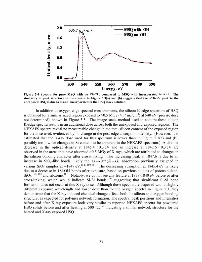
73
Figure 5.4 Spectra for pure MSQ with no , compared to MSQ with incorporated . The
similarity in peak structure to the spectra in Figure 5.3(a) and (b) suggests that the ~536 eV peak in the
unexposed HSQ is due to incorporated in the HSQ stock solution.
In addition to oxygen edge spectral measurements, the silicon K-edge spectrum of HSQ
is obtained for a similar sized region exposed to >0.5 MGy (>17 mJ/cm2) at 540 eV (precise dose
not determined), shown in Figure 5.5. The image stack method used to acquire these silicon
Kedge spectra results in an additional dose across both the unexposed and exposed regions. The
NEXAFS spectra reveal no measureable change in the total silicon content of the exposed region
for the dose used, evidenced by no change in the post-edge absorption intensity. (However, it is
estimated that the Xray dose used for this spectrum is lower than in Figure 5.3(a) and (b),
possibly too low for changes in Si content to be apparent in the NEXAFS spectrum.) A distinct
decrease in the optical density at 1845.4 ± 0.3 eV and an increase at 1847.6 ± 0.3 eV are
observed in the areas that have absorbed >0.5 MGy of X-rays, which are attributed to changes in
the silicon bonding character after cross-linking. The increasing peak at 1847.6 is due to an
increase in SiO2like bonds, likely the )(*1 OSis absorption previously assigned in
various SiO2 samples at ~1847 eV.152, 160-161
The decreasing absorption at 1845.4 eV is likely
due to a decrease in bonds after exposure, based on previous studies of porous silicon,
SiO2,160, 162
and siloxene.161
Notably, we do not see any feature at 1838-1840 eV before or after
cross-linking, which would indicate Si-Si bonds,160
suggesting that significant Si-Si bond
formation does not occur at this X-ray dose. Although these spectra are acquired with a slightly
different exposure wavelength and lower dose than for the oxygen spectra in Figure 5.3, they
demonstrate that the Xray induced chemical change affects both the silicon and oxygen bonding
structure, as expected for polymer network formation. The spectral peak positions and intensities
before and after X-ray exposure look very similar to reported NEXAFS spectra for powdered
HSQ solids before and after heating at 500 °C,163
indicating a similar network structure for the
heated and Xray exposed HSQ.

74
Figure 5.5 Silicon K-edge NEXAFS spectra HSQ film (~250 nm thick), showing a decrease in OD at
1845.4 eV and an increase at 1847.6 eV after >0.5 MGy Xray exposure at the oxygen edge (540 eV),
indicating an increase in SiO2-like structure but no change in total silicon content.
5.4 X-ray induced cross-linking reaction rate
The change in the NEXAFS spectra between exposed and unexposed HSQ is a measure
of the structural transformation due to the chemical reaction. After patterning HSQ thin films
with the X-ray beam, the patterned area is imaged at 536 eV. There is no further sample
modification prior to this imaging, such as development in solution; the contrast at each spatial
location in the image is calculated in ΔOD (Eq. 5.2), which quantifies the relative degree of
cross-linking in the exposed vs. unexposed areas. The sensitivity is defined here as the increase
in contrast per unit of absorbed Xray dose. These definitions of contrast and sensitivity are
based solely on the photochemical characteristics of the HSQ thin films, but are analogous to
those typically used for lithography, which are based on developer effects.2 The relation of the
unexposed contrast and sensitivity to the development effects are discussed in section 5.6.
To examine the X-ray exposure sensitivity of HSQ and relate contrast (ΔOD) to the
degree of cross-linking, the HSQ films are patterned at increasing dose and then imaged, shown
in Figure 5.6(a). Equal-sized 1 μm × 5 μm features are exposed in a pre-baked, 500 ± 50 nm
thick HSQ film by direct-write Xray patterning, in this case at an energy of 536 eV, at doses
from 2.0 ± 0.4 to 276 ± 57 MGy. The spacing between exposure points within each feature is
200 nm, features are separated by 1 μm, and the dwell time is increased exponentially for each
subsequent feature. The patterned area is subsequently imaged at 536 eV, and the Xray
transmission through each feature is shown in Figure 5.6(a), where the line profile indicates the
average contrast through the shaded region highlighted by the bold arrows, and the black spots
are clusters of 100 nm gold nanoparticles on the film surface (used for focusing). Though the
point spacing is 200 nm, the individual exposed points are not observed within each feature due
to significant spreading of the cross-linking reaction beyond the 50 nm exposure beam width,
which is explained in detail in the subsequent section. The contrast between the exposed and
unexposed regions, which is a measure of the relative degree of cross linking, is plotted versus
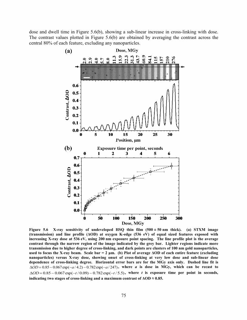
75
dose and dwell time in Figure 5.6(b), showing a sub-linear increase in cross-linking with dose.
The contrast values plotted in Figure 5.6(b) are obtained by averaging the contrast across the
central 80% of each feature, excluding any nanoparticles.
Figure 5.6 X-ray sensitivity of undeveloped HSQ thin film (500 ± 50 nm thick). (a) STXM image
(transmission) and line profile (ΔOD) at oxygen K-edge (536 eV) of equal sized features exposed with
increasing Xray dose at 536 eV, using 200 nm exposure point spacing. The line profile plot is the average
contrast through the narrow region of the image indicated by the grey bar. Lighter regions indicate more
transmission due to higher degree of cross-linking, and dark points are clusters of 100 nm gold nanoparticles,
used to focus the X-ray beam. Scale bar = 2 μm. (b) Plot of average ΔOD of each entire feature (excluding
nanoparticles) versus X-ray dose, showing onset of cross-linking at very low dose and sub-linear dose
dependence of cross-linking degree. Horizontal error bars are for the MGy axis only. Dashed line fit is
)247/exp(782.0)2.4/exp(067.085.0 aaOD , where a is dose in MGy, which can be recast to
)5.5/exp(782.0)09.0/exp(067.085.0 ttOD , where t is exposure time per point in seconds,
indicating two stages of cross-linking and a maximum contrast of ΔOD ≈ 0.85.
76
The double exponential curve fit in Figure 5.6(b) indicates a two-stage cross-linking
process, with a fast initial step with τ1 = 0.09 ± 0.01 s and a much slower second stage with
τ2 = 5.5 ± 0.3 s. Just as reaction rates typically depend on temperature or laser power, these time
constants vary based on the rate of energy absorption, or absorbed dose rate; here the incident
flux is ~1.6 x 10⁶ photons/s, corresponding to an absorbed dose rate of approximately 42 MGy/s.
The fit shows that the cross-linking can continue well beyond the maximum dose used here of
276 ± 57 MGy (19,339 ± 3203 mJ/cm2), up to a maximum contrast of ΔOD ≈ 0.85 for the fully
cross-linked material. Assuming that ΔOD = 0 - 0.85 corresponds to 0 - 100% relative degree of
cross-linking, an increase in contrast of ΔOD = 0.1, for example, equates to an increase in the
degree of cross-linking of 11.8 ± 4.2 % out of the possible cross-linkable sites. A linear fit of the
lowest-dose points in Figure 5.6(b) gives an initial sensitivity of 1.1 ± 0.4 % cross-linking
increase per MGy Xray dose, while the highest-dose points give a final sensitivity of
0.19 ± 0.07 % per MGy. Thus the initial, fast cross-linking corresponds to higher sensitivity, and
the slower cross-linking is equivalent to lower sensitivity.
This double exponential decay in the cage-like species is analogous to the NIR MAP
mechanism of HSQ, where the slower cross-linking reaction rates (τ1 = 30 ± 10 s and
τ2 = 3 ± 1 min, section 3.3)79
are presumably due to a lower dose rate and possibly a different
mechanism. As mentioned previously, one explanation for the two time stages is that as reactive
sites are generated photolytically in the solid film, nearby sites react quite readily, but the rigidity
of the network increases with cross linking. This slows the rate of additional cross-linking due to
the restricted mobility of the remaining reactive sites, which are locked into the polymer network
configuration. Another way of saying this is if there are some bonds with more favorable
kinetics for cross linking due to juxtaposition or angular geometry, these may cross-link first,
giving the initial faster cross-linking rate, which slows as these sites are used up.
5.5 Area dependent sensitivity
For the increasing dose features in Figure 5.6(a), no significant increase in cross-linking
is observed in between features at low dose, but an increasing background level of cross-linking
is measured in between the adjacent features starting at a dose of 22.3 MGy (1563 mJ/cm2,
position ~16 μm), indicating that increased cross-linking occurs well outside the exposed region.
To the right of the highest dose feature, an increase in cross-linking giving ΔOD ≈ 0.03 is
observed more than 1 μm beyond the exposure boundary, which is nearly the amount of cross-
linking observed at the center of the 2.0 MGy exposed feature. This extensive diffusion of the
polymer cross-linking is consistent with previous STXM and FTIR imaging of undeveloped
ebeam exposed HSQ films, where a small but measurable increase in cross-linking was
observed at distances greater than 12 μm away from the e-beam exposed regions at very high
doses.50, 68
Based on previous reports with HSQ, some area dependent contrast is expected,8, 51
defined here as an increase in peak contrast as the feature size increases, despite a constant
absorbed dose. This can be interpreted as a higher sensitivity for the larger features, because to
obtain features with an equivalent peak degree of cross-linking (a requirement for some
lithography applications2, 8
) would require decreasing the dose significantly for larger features.
The amount of peak contrast is highly dependent on the overlap between exposed points,51
but
likewise should depend on the overlap of regions cross-linked by reaction spread beyond the
77
exposure boundary. To examine how the lateral reaction spread contributes to the area
dependent sensitivity, a set of features with different sizes are patterned at constant dose of
8.6 ± 1.4 MGy (484 ± 44 mJ/cm2) in an unbaked, 400 ± 50 nm thick HSQ film, then imaged at
536 eV, shown in Figure 5.7(a). The first feature on the left in Figure 5.7(a) is a single-pass line
exposure of the Xray beam at 580 eV with 50 nm point spacing, and the exposed width of the
features is increased going to the right, up to 1.5 μm wide for the right-most feature, made by 30
adjacent single-pass lines separated by 50 nm. Figure 5.7(b) is a plot of the increase in the peak
contrast versus exposed feature width [from Figure 5.7(a)]. There is only a slight overlap
between adjacent point exposures within each feature, so only a small increase in peak cross-
linking is expected with feature width, shown as the bottom dashed line (black) in Figure 5.7(b);
however, the data clearly shows a much stronger area dependence. Furthermore, the measured
FWHM of the single line exposure in Figure 5.7(a) is 360 ± 50 nm, showing a spread of cross-
linking of at least 150 nm laterally from the edges of the exposure beam. The upper dashed
curve (gray) in Figure 5.7(b) simulates the peak degree of cross linking expected with a 360 nm
beam width, which more closely resembles the observed measurements. The simulated curves
are for isolated features with 50 nm point spacing at ~8.6 MGy, using the exposure beam profile
in Figure 5.1(a) (50 nm or 360 nm FWHM) and the HSQ sensitivity from Figure 5.6(b). The
observed increase in peak cross-linking is even higher than the wider-beam simulation because
of the long tail of the cross-linking spread, which causes increased overlap between features that
are too closely spaced (evidenced by the increasing background in between features in Figure
5.7(a)). Note that the integrated intensity of the line profiles for the data and simulations here
show that the total degree of cross-linking is approximately linear with increasing feature width.
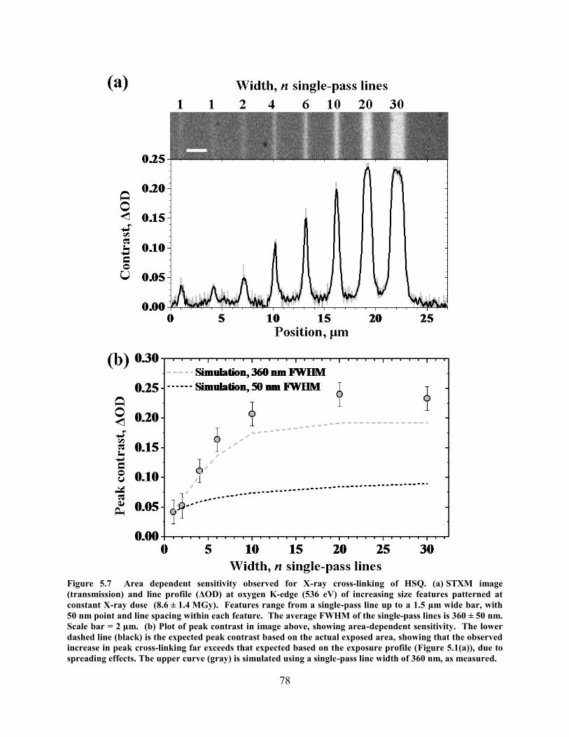
78
Figure 5.7 Area dependent sensitivity observed for X-ray cross-linking of HSQ. (a) STXM image
(transmission) and line profile (ΔOD) at oxygen K-edge (536 eV) of increasing size features patterned at
constant X-ray dose (8.6 ± 1.4 MGy). Features range from a single-pass line up to a 1.5 μm wide bar, with
50 nm point and line spacing within each feature. The average FWHM of the single-pass lines is 360 ± 50 nm.
Scale bar = 2 μm. (b) Plot of peak contrast in image above, showing area-dependent sensitivity. The lower
dashed line (black) is the expected peak contrast based on the actual exposed area, showing that the observed
increase in peak cross-linking far exceeds that expected based on the exposure profile (Figure 5.1(a)), due to
spreading effects. The upper curve (gray) is simulated using a single-pass line width of 360 nm, as measured.

79
The strong area-dependence of the peak contrast is attributed to the spread in the cross-
linking beyond the exposure boundaries. As the pixel spacing is significantly less than the
distance of the reaction spread, each adjacent line within a feature will overlap previously cross-
linked material, and the peak of the cross-linking will accumulate to a higher degree than
anticipated based on the absorbed dose alone. The peak contrast levels off at a width of
approximately 10 single-pass lines, because once the feature is significantly wider than the
reaction spread, the overlap between partially exposed regions becomes primarily an edge effect.
Interestingly, for cases up to 10 adjacent single-pass lines, the area dependence of the peak
contrast is also approximately linear, as previously reported for area dependence measurements
in ultra-thin, e-beam patterned and developed HSQ.51
Preliminary results suggest that the area
dependence and linewidth vary somewhat with the delay time between film preparation (spin-
coating) and exposure, as do the film contrast and sensitivity, consistent with previously
published studies of e-beam patterning in HSQ.2, 48-49, 164
This proximity effect is also extremely important for small features that are closely
spaced. To demonstrate this, adjacent pairs of single-pass lines are written at various distances
apart (125 nm to 2 μm) at three different doses from 7.2 to 28 MGy (405 to 1590 mJ/cm2). As
shown in Figure 5.8, even at the lowest dose of 7.2 ± 1.5 MGy, the overlap between adjacent
lines is so significant that the two separate lines can not be discerned until they are separated by
at least 500 nm. At all doses, adjacent lines must be spaced by >1 μm in order to prevent some
overlap and measurable latent contrast in between adjacent features. The simulated data in
Figure 5.8(b) shows that well separated lines are expected if the reaction does not spread beyond
the exposure boundaries, based on the X-ray exposure beam profile and HSQ sensitivity. For
comparison, the simulated data in Figure 5.8(c) shows that a reaction spread of 390 nm for a
single-pass line (FWHM) approximately matches the measured feature profiles, but with slightly
higher peak contrast, possibly due to uncertainty in the exact shape of the reaction spread profile.

80
Figure 5.8 Proximity effects measured for pairs of single-pass lines separated by different distances at
constant dose, 7.2 ± 1.5 MGy (point spacing = 50 nm), shown in STXM image (top) and line profile (bottom)
at the oxygen K-edge (536 eV). Gray profile is raw data, black is smoothed. The more closely spaced lines
cannot be discerned due to the reaction spread. Scale bar = 1 μm. Profiles at right show simulated lines
(black) overlaid on smoothed data (gray) for (b) 50 nm exposure beam profile (FWHM) and (c) 390 nm beam
profile, indicating that reaction diffuses outside of the 50 nm wide exposed region to a FWHM of ~390 nm.
Peak contrast and linewidth cannot be fit simultaneously, possibly due to uncertainty in the reaction spread
profile.
5.6 Quantifying reaction spread
Based on the results in Figure 5.6, Figure 5.7, and Figure 5.8 and previous studies of
undeveloped e-beam patterns in HSQ,50, 68
it is apparent that the spatial extent of the reaction
spread depends upon the exposure dose. Since the proximity effects in Figure 5.7 and Figure 5.8
are determined by how far the reaction spreads from each exposed point, the dose dependence of
this spread needs to be well defined for useful lithography in order to achieve the desired degree
of cross-linking for a given feature size, as it relates to the final height of the developed features.
To measure the extent and shape of this spread with good signal-to-noise, many sets of single-
pass line exposures with doses from 0.4 to 111 MGy are produced (50 nm point spacing, 580 eV
exposure), and these sets of lines are repeated many times in different films which are 100-400
nm thick. Figure 5.9(a) shows the raw X-ray transmission image for a set of undeveloped, X-ray
exposed lines in a 330 ± 50 nm thick HSQ film after patterning, and line profiles, vertically
averaged along the full length of each line in ΔOD, which are used to obtain the FWHM. The
FWHM of all the undeveloped single-pass lines are shown in Figure 5.9(b), where each point is
the mean line width of 2-5 independent lines patterned at that dose. These lines are, of course,
substantially wider than in recent state-of-the-art HSQ lithography (4.5 to 20 nm line width),1-2, 55
due to the film thickness and 50 nm FWHM exposure beam, as well as the delay between baking
and exposure,2, 48-49, 164
and possibly due to the ~2 year storage of the HSQ stock solutions.48
The

81
area, dose and thickness dependent trends observed here agree with trends reported for thin HSQ
e-beam and photo-lithography.2
Figure 5.9 Single-pass lines used to quantify the diffusion of the cross-linking reaction. (a) STXM image
(transmission) and line profile (ΔOD) at oxygen K-edge (536 eV) for undeveloped lines exposed at doses from
0.6 ± 0.3 to 111 ± 29 MGy with 50 nm point spacing. Small gap in image and plot is where no data was taken.
All cross-linked material below the dashed line was washed away by subsequent development. (b) Plot of
undeveloped line widths, FWHM, showing a strong dependence of the width on both dose and sample
thickness. Narrowest lines are in ~300 nm thick films (open triangles). An increase in line width is observed
in ~330 nm thick films (filled circles) and 400 nm thick films (gray squares). (c) SEM image and (d) STXM
image (transmission) with line profile (OD) at 536 eV of the same lines after development, showing the onset
of developer at an exposure dose of 3.9 ± 1.0 MGy. Note that the absolute contrast in this plot cannot be
compared with the contrast in (a), as the unexposed film has been washed away by the developer. (e) Plot
comparing developed (gray circles) and undeveloped (black circles) line widths, FWHM from STXM data in
~330 nm thick film, showing similar but slightly sharper line widths after development at low doses, due to
removal of the partially cross-linked material at the line edges. Surprisingly, the highest dose lines
(111 MGy) have a greater FWHM after development, even though they are narrower at the base. SEM
measurements of developed lines in 100 nm thick films (open circles) are considerably narrower, continuing
the trend of narrower lines in thinner films. Scale bars = 1 μm.
Figure 5.9(b) shows that there is a substantial spread in the HSQ cross-linking beyond the
exposed region in the undeveloped films, which increases with exposure dose and with film
thickness. For the ~300 nm thick films, the minimum possible line width is 157 ± 5 nm,
compared to 190 ± 7 nm for the ~330 nm thick films, and 223 ± 27 nm for the ~400 nm thick
films, determined by fitting a line through the low dose points only and extrapolating to zero
82
dose. This increase in line width with film thickness is consistent with recently published results
for very thin, developed HSQ.51, 165
Taking into account the three-dimensional spread of the
reaction upon exposure, one possible explanation for the greater reaction spread with thicker
films is that the process responsible for the reaction spread is inhibited by the surface of the film.
In addition to this thickness dependence, the spread in the reaction increases with dose, as
expected.51
For example, in the 330 nm thick film, the linewidth averages 193 ± 40 nm FWHM
at the low dose of 0.6 ± 0.5 MGy, up to 355 ± 7 nm at a dose of 111 ± 29 MGy, corresponding to
a spread of 70-150 nm on either side of the exposure beam profile at the FWHM. Note the two-
stage shape of the increase in linewidth with dose, as the linewidth initially increases very
sharply with dose, then the rate of linewidth increase slows considerably with additional dose,
even up to very high doses. This indicates two different possibilities, which are not mutually
exclusive; it could indicate a maximum range for the diffusing species or chain reaction, or it is
also consistent with the double exponential decay mechanism mentioned above (Figure 5.6),
where the initial cross-linking sensitivity of the HSQ to diffusing species is very high, but the
cross-linking effectiveness decreases once a certain degree of cross-linking has been reached.
For comparison, Figure 5.9(c) shows an SEM image of the same set of lines [from Figure
5.9(a)] after room temperature development in 1% NaOH + 4% NaCl. Figure 5.9(d) shows the
STXM transmission at 536 eV of these developed lines and the line profile of this image
converted to OD. The single-pass lines exposed at low doses, 0.6 ± 0.3 and 2.1 ± 0.6 MGy, are
removed by the developer, while the features at 3.9 ± 1.0 MGy (181 ± 37 mJ/cm2) dose are just
visible. Following the typical definition of onset dose (Di, the minimum dose for which the
cross-linked resist is insoluble in the developer), this corresponds to an onset dose of ~3.9 MGy
(~181 mJ/cm2), which agrees very well with the onset dose for previously reported X-ray
lithography in 300 nm thick HSQ films of Di ≈ 200 mJ/cm2 (in TMAOH developer).
41
Figure 5.9(e) is a plot of the FWHM of these undeveloped and developed lines, which
shows that the developed lines are just slightly narrower at low doses. However, at a high dose
of 111 MGy, the FWHM of the developed lines are actually ~30% wider, even though these lines
are still narrower at their base after development. In addition, the 90 ± 14 nm wide lines at
7.1 ± 2.4 MGy (100 ± 32 mJ/cm2) in the developed 100 ± 20 nm thick HSQ film are plotted in
Figure 5.9(e), continuing the observed trend of narrower lines in thinner samples beyond the
minimum thickness accessible by latent STXM imaging. The dashed line in Figure 5.9(a)
corresponds to the cutoff in latent contrast below which the developer removes all material,
which is at a ΔOD value of 0.06 ± 0.02. The developed lines have a slightly different line shape
because the material below this critical cross-linking degree (ΔOD ≈ 0.06), at the edges of the
lines near the base, is removed by the developer. This narrowing of the lines is expected based
on studies of the developer activity,166
but detailed line profiles of the undeveloped material were
not accessible in that work. By assuming that ΔOD = 0 - 0.85 corresponds to 0 - 100% relative
degree of cross-linking [Figure 5.6(b)], the critical cross-linking degree for development contrast
(ΔOD=0.06) corresponds to an increase in the degree of cross-linking of just 7.1 ± 2.5 % out of
the possible cross-linkable sites. Previous FTIR studies of HSQ thin films approximate the
minimum and maximum possible conversion degree to be 19.4% - 70%,68
where conversion
degree is defined as the ratio of cage bonds to network bonds. Some HSQ
cross-linking occurs during film preparation, even for room-temperature preparation under
vacuum,35, 47
and the initial degree of cross-linking also depends on whether the sample is pre-
baked, for how long and at what temperature,47, 57
the delay after spin-coating, and storage
atmosphere.48-49
Importantly here, it also depends upon the age of the stock solution subsequent

83
to manufacture.48
If we assume a starting cross-linking degree for the entire film of 19.4% and a
maximum of 70%, based on previous FTIR work,68
the developer onset of ΔOD=0.06 would
correspond to an absolute cross-linking degree of approximately 24%. However, due to the
aging and delay effects, and other variations between samples, the starting degree of cross-
linking in these particular films is uncertain, likely higher than 19.4%. It is important to note that
although only the relative degree of cross-linking (latent contrast) can be measured here, the
onset dose of the developer also depends upon the absolute degree of cross-linking.
The line widths in Figure 5.9 were compared to the single-pass lines in Figure 5.7, and it
was observed that the longer delay between film preparation and exposure used for the data in
Figure 5.7 (70 hours, due to beam time constraints) resulted in significantly wider lines and
lower contrast for comparable doses. Previous reports show that a delay between baking and
exposure can lead to such line width broadening,49
and that the magnitude of the contrast
changes with post-bake delay can exceed the sample aging effects,48
but the preliminary data
comparison in this study suggests that the delay effect may be an issue even in these films which
are unbaked. Thus, in future work the delay between spin-coating and exposure should be
minimized and much more carefully controlled.
By comparing the undeveloped STXM image contrast in Figure 5.6(a) and Figure 5.9(a)
with previously reported STXM images of e-beam exposed HSQ, it is possible to approximate
the relationship between X-ray dose and e-beam dose. From this, we estimate that the developer
onset X-ray dose of ~3.9 MGy (~181 mJ/cm2) in this film corresponds to a 100 keV ebeam dose
of approximately 8 ± 4 mC/cm2 in a 250 nm thick HSQ film (pre-baked at 170 °C for 5 min).
50
This comparison is only an approximate frame of reference for the doses used in the current
study, as there were significant differences between the sample used in the e-beam study and the
present work, including the precise film thickness, exposure point spacing, sample age, delay and
pre-bake conditions. Nonetheless, our onset dose of 3.9 MGy ≈ 8 ± 4 mC/cm2 agrees within
error to the previously reported onset dose of 6.5 mC/cm2 under the same developer conditions in
115 nm thick HSQ.151
5.7 Potential mechanisms for cross-linking reaction spread
The main result of this work is to quantify the X-ray exposure sensitivity and reaction
spread in undeveloped HSQ patterns. Since the X-ray beam position is interferometer controlled
to better than 10 nm and tightly focused, and we have carefully measured and accounted for the
initial (low-dose) sensitivity of HSQ, exposure effects leading to line broadening can be ruled
out. One possible cause for the >70 nm lateral spread of the reaction could be reactive species
diffusing through the film to the unexposed regions. Reaction spread beyond the exposure
boundaries within this range has recently been reported in other X-ray patterned, thin (~40 nm),
organic positive-tone photoresist materials (PMMA and PAN). The results are tentatively
attributed to the propagation of radicals and/or ions through the film, but the mechanism has yet
to be determined.82
In that report, it was estimated that, given the conditions of 300 Torr of He
in the X-ray exposure, heating of the films is negligible (on the order of 5 x 10⁻⁴
K), and that
thermal damage is therefore an unlikely mechanism for the reaction spread.
As explained in section 2.3, when the soft X-ray photon at 536 eV to 580 eV is absorbed
by the HSQ thin film, it excites a core electron in the sample, which decays to produce a high
energy Auger electron (~500 eV) and a singly or doubly ionized valence excited state, which can
84
lead to the breaking of nearby bonds at a range of a few nm. This likely results in energetic and
reactive radical and/or ion fragments, and secondary electrons, which can further propagate the
initiation of the reaction.82
The mean free path of scattered 0-580 eV electrons in HSQ should be
similar to amorphous glass and polymers of similar density, which is less than 10 nm.167-168
The
effect of low energy secondary electrons (10-50 eV) in e-beam lithography of HSQ was shown
to be limited to a range of ~2 nm.169
Therefore we suspect that small radicals or ions are
responsible for the >70 nm reaction spread through the film. The single bond is
significantly weaker than typical single bonds (~4.08 eV versus ~8.95 eV each,
respectively).43
It is possible that protons or H radicals are liberated by the cleavage of the
bonds during the Xray absorption, and these may be able to propagate some distance before
reacting and causing cross-linking, possibly leading to a cross-linking chain reaction.
A variety of mechanisms could explain the reaction spread, and here we discuss two
possibilities in more detail. Electron spin resonance (ESR) studies indicate that H radicals
produced upon gamma irradiation of crystalline HSQ can travel through the solid to neighboring
cages;170-171
this species may also propagate through a silicon-based polymer (reported for poly-
dimethylsiloxane, PDMS) before abstracting an additional H atom to form H2 and a molecular
radical that cross-links.172-173
Therefore, one possibility is that H radicals produced by the X-ray
induced bond breaking in HSQ travel through the film to abstract H from another
bond 70 nm or more away, creating an additional silicon radical:
(5.7)
where the symbol again represents all the additional cage or network bonds on the Si atom.
This silicon radical could then cross-link with a neighboring HSQ cage in a variety of ways,
possibly involving the uptake of water to form a reactive silanol,37
or cage bond redistribution,35-
36, 173 as shown in Figure 4.6. However, since the silicon radical is bound to the network, unlike
the H radical, and because free radicals in solid polymers must be separated by less than ~4 Å in
order to react,174
continued spread of cross-linking by a silicon-radical induced chain reaction is
less likely within the solid HSQ film. Without such a chain reaction, each H radical would
initiate only one cross-linking event, and substantial cross-linking at a distance would depend
upon H atoms diffusing through the film from the exposed region.
An alternative, acid-catalyzed reaction could be initiated by protons according to the
following mechanism:
(5.8)
Subsequently, the proton is regenerated by reaction of the silicon cation with moisture, which
subsequently gives an additional source of reactive silanol bonds:
(5.9)
This proton-initiated mechanism could lead to significant line width spread from a small number
of protons, as the catalytic reaction propagates to form many additional cross-links. Recent work
shows that HSQ is extremely sensitive to proton beam exposure, but suggests that there are
almost no proximity effects when using high energy protons (2 MeV),39
suggesting that this
proton-initiated chain reaction does not occur under those conditions. On the other hand,
85
preliminary STXM results on ebeam exposed HSQ patterns show that some reaction spread
continues for more than a day after ebeam exposure, which would indicate that a very slow
chain reaction is in fact occuring.175
One possible explanation is that the H radical mechanism of
the previous paragraph does occur initially, but the silicon radicals left over continue to react
much more slowly over time, due to the rigidity of the network HSQ structure. In either case
(protons or radicals), interactions at the film surface are expected to inhibit the reaction spread,
resulting in narrower lines in thinner films, as observed.
H atoms and protons have similar diffusion coefficients through glasses at room
temperature, on the order of ~10-7
cm2/s for protons in porous sol-gel glasses (highly dependent
on pore size)176
and 10-6
-10-7
cm2/s for H atoms in amorphous silica,
177 both of which have
structures similar to cross-linked HSQ. This can result in one-dimensional diffusion of ~100 nm
in just 5 to 16 ms, so the spread of these species from one single-pass line would be complete
before an adjacent line is patterned, as each single-pass line in the present study requires
>200 ms writing time. If hydrogen radicals or protons are responsible for the spread in the cross-
linking, then the incorporation of molecules designed to trap such species should lead to a
reduction in the line width spread, and experiments to test this hypothesis are desirable.
Preliminary patterning results in films with added inhibitors are discussed in Chapter 6.
Both of these mechanisms can explain the decrease in (silanol) content and the
increase in oxygen content with cross-linking observed in the NEXAFS spectra in this study
[Figure 5.3(a)]. The increase in oxygen may be partially due to creation of new, transient
groups via reaction with protons and/or moisture, which then react with each other to
form cross-links (Eq. 4.14 and 5.6). These new groups can also react with existing
groups, thereby decreasing the total content (Eq. 4.17). As the initial
content is expected to be quite small and would enhance the film sensitivity, the fast initial cross-
linking stage also fits with this hypothesis. As noted earlier with respect to the oxygen edge
NEXAFS spectra, the amount of adsorbed water may increase during cross-linking due to
changes in hydrophobicity and porosity, which would also lead to the observed increase in the
total oxygen content of the cross-linked regions. Morphological and hydration changes will also
alter the diffusion constant during cross-linking, and indeed a quantitative analysis by us with a
simple Fickian diffusion model does not explain the rather abrupt rise and saturation of the
linewidth increase versus dose (Figure 5.9(b)) and cross-linking rate (Figure 5.6 (b)). Therefore,
to fit all of the experimental data and retrieve diffusion coefficients for the propagating reactive
species would require more detailed theoretical modeling, taking into account changes in the
diffusion constant over time, the changing rate constant as evidenced by the two-stage,
apparently first-order kinetics, and surface effects that explain the thickness dependence.
5.8 Conclusions
Direct-write X-ray lithography and subsequent X-ray imaging of the latent resist patterns
is a powerful way to follow the chemistry of X-ray induced processes in the absence of
developer effects. Oxygen and silicon edge NEXAFS spectra of the HSQ film before and after
X-ray exposure show that the total oxygen content in X-ray exposed regions increases
substantially, by ~30% at 808 MGy and less at lower doses, while the content decreases,
and no change in the silicon content is observed. This indicates that existing is
consumed by incorporation into the network and that there is an uptake of water and/or

86
additional incorporated oxygen in the X-ray cross-linked regions. The sensitivity of HSQ to
direct X-ray exposure reveals that the cross-linking proceeds by a very fast initial step
(τ1 = 0.09 ± 0.01 s) followed by a slower second stage (τ2 = 5.5 ± 0.3 s), which suggests that there
are initially some number of easily cross-linked sites, and that the reaction rate slows
considerably after these sites are consumed.
Direct-write X-ray lithography and subsequent X-ray imaging of the latent patterns with
30 nm resolution reveals a dose and thickness dependent reaction front spread in excess of 70 nm
in HSQ films independent of developer conditions, which is crucial to understanding the
resolution-limiting characteristics of HSQ and correcting for proximity effects. The long range
of this dose and thickness dependent reaction spread is likely due to the diffusion of some small
ions or radicals through the HSQ film, and we provide two possible mechanisms based on
diffusing H atoms or protons. The full extent of this spread is not apparent after high-contrast,
room-temperature development, as the developer solution removes material below a critical,
relative cross-linking degree of 7.1 ± 2.5% (relative to the maximum number of cross-linkable
sites within the film), whether it is cross-linked by direct exposure or reaction spread. While the
STXM imaging requires thick HSQ films (>250 nm) for good signal-to-noise ratios, the
chemical information and line width versus thickness trends appear to be applicable for thinner
films, as well.
Future X-ray work on HSQ can address the role of water and in the X-ray
induced cross-linking mechanism and test if H radical or proton diffusion is responsible for the
reaction spread outside the exposed region. Preliminary results with various reaction-spread
inhibitors are discussed in Chapter 6. The next generation of Fresnel zone plates for X-ray
microscopy, with 12-15 nm outer diameters,10-12
will significantly improve the resolution
possible with both direct-write X-ray lithography and STXM imaging. As HSQ is the resist used
for fabrication of these gold zone plates, higher resolution X-ray microscopes are made possible
in part by a better understanding of HSQ chemistry. Furthermore, with a better understanding of
the cross-linking mechanism, delay effects and the cause of the reaction spread, new and better
photoresists based on HSQ can be designed to fabricate the next generation of smaller, faster,
more reliable electronic devices, and other new nanoscale device components.
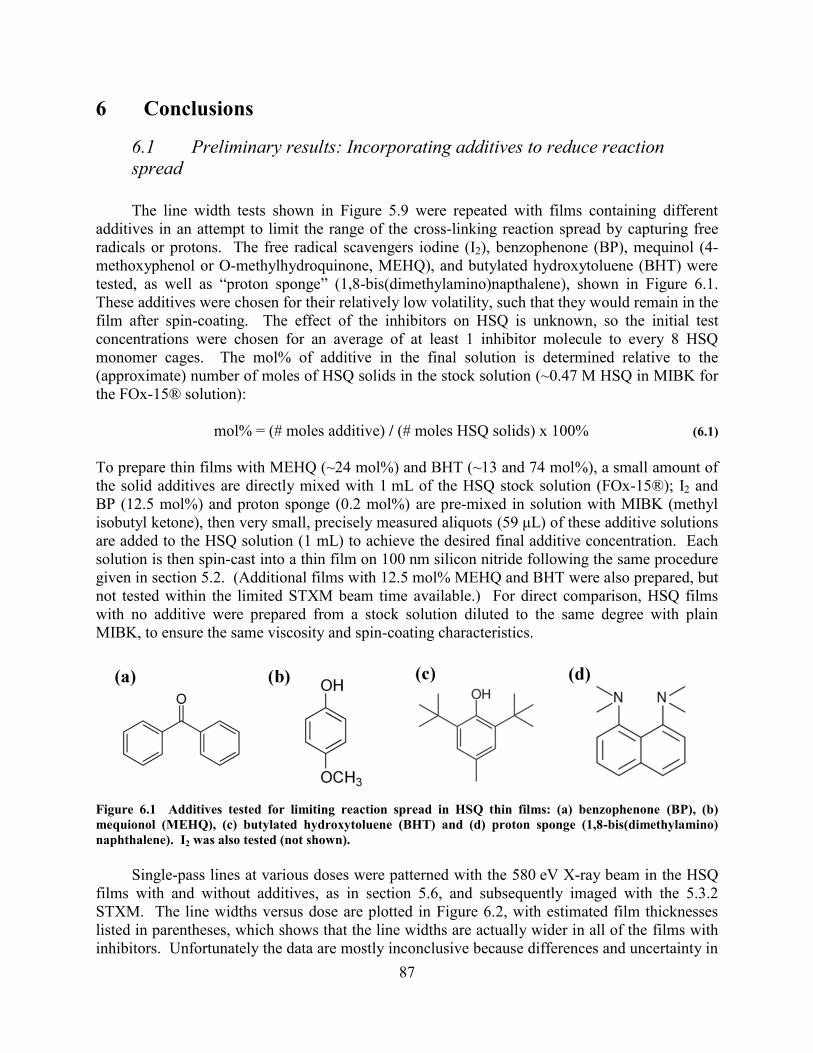
87
6 Conclusions
6.1 Preliminary results: Incorporating additives to reduce reaction
spread
The line width tests shown in Figure 5.9 were repeated with films containing different
additives in an attempt to limit the range of the cross-linking reaction spread by capturing free
radicals or protons. The free radical scavengers iodine (I2), benzophenone (BP), mequinol (4-
methoxyphenol or O-methylhydroquinone, MEHQ), and butylated hydroxytoluene (BHT) were
tested, as well as “proton sponge” (1,8-bis(dimethylamino)napthalene), shown in Figure 6.1.
These additives were chosen for their relatively low volatility, such that they would remain in the
film after spin-coating. The effect of the inhibitors on HSQ is unknown, so the initial test
concentrations were chosen for an average of at least 1 inhibitor molecule to every 8 HSQ
monomer cages. The mol% of additive in the final solution is determined relative to the
(approximate) number of moles of HSQ solids in the stock solution (~0.47 M HSQ in MIBK for
the FOx15® solution):
mol% = (# moles additive) / (# moles HSQ solids) x 100% (6.1)
To prepare thin films with MEHQ (~24 mol%) and BHT (~13 and 74 mol%), a small amount of
the solid additives are directly mixed with 1 mL of the HSQ stock solution (FOx15®); I2 and
BP (12.5 mol%) and proton sponge (0.2 mol%) are pre-mixed in solution with MIBK (methyl
isobutyl ketone), then very small, precisely measured aliquots (59 μL) of these additive solutions
are added to the HSQ solution (1 mL) to achieve the desired final additive concentration. Each
solution is then spin-cast into a thin film on 100 nm silicon nitride following the same procedure
given in section 5.2. (Additional films with 12.5 mol% MEHQ and BHT were also prepared, but
not tested within the limited STXM beam time available.) For direct comparison, HSQ films
with no additive were prepared from a stock solution diluted to the same degree with plain
MIBK, to ensure the same viscosity and spin-coating characteristics.
Figure 6.1 Additives tested for limiting reaction spread in HSQ thin films: (a) benzophenone (BP), (b)
mequionol (MEHQ), (c) butylated hydroxytoluene (BHT) and (d) proton sponge (1,8-bis(dimethylamino)
naphthalene). I2 was also tested (not shown).
Single-pass lines at various doses were patterned with the 580 eV Xray beam in the HSQ
films with and without additives, as in section 5.6, and subsequently imaged with the 5.3.2
STXM. The line widths versus dose are plotted in Figure 6.2, with estimated film thicknesses
listed in parentheses, which shows that the line widths are actually wider in all of the films with
inhibitors. Unfortunately the data are mostly inconclusive because differences and uncertainty in

88
the film thicknesses and delay effects mask potential differences due to the additives. First of all,
line widths can only be directly compared between films with the same thickness, but variations
in film thickness from region to region make it extremely difficult and prohibitively time
consuming to find regions that are comparable from film to film. In the previous chapter, this
was solved only by taking many, many measurements on identical films, and only comparing
regions with equivalent thickness; each measurement is still quite time consuming, and so far,
not enough data have been collected on inhibitor-added films to achieve this. Second, variations
in film composition and density due to the additives increase the uncertainty in the thickness
measurements, which are based on the OD 1 nm spectrum of HSQ with a fixed density
(1.4 g/cm3) (see Figure 5.2(a)). To circumvent these film thickness issues, it is desirable to have
films of uniform thickness and then measure the thickness by an alternative method, such as
ellipsometry or AFM. Two alternative methods for producing uniform thickness films were
explored and tested, but neither was feasible within the parameters of these studies.
Figure 6.2 Average FWHM line widths for single-pass lines in HSQ films varying from 250 nm to 425 nm
thick with various radical and proton scavenger molecules added (a) Full range of doses tested and (b)
zoomed in to low dose. Legend at right, with estimated film thicknesses shown in parentheses, and time delay
between spin-coating and exposure listed in brackets.

89
A third complication may be delay effects, as line widths have been shown to increase
significantly (greater than 100% in 8 hours) with delay between film pre-bake and exposure,
measured after development.49
Preliminary results with the STXM reveal similar line width
broadening when there is a delay between spin-coating and exposure, even in unbaked samples.
In the inhibitor-added films, there is a different time delay between film spin-coating and
exposure for several of the measurements, due to STXM beam-time constraints, sample loading
and positioning times, and trial and error in finding suitable areas of each sample for patterning
and measurement. That is, different samples were measured between 34 to 74 hours after spin-
coating, with the delay time listed in brackets in the legend on Figure 6.2. The line widths
appear to be larger in films subjected to a greater delay between spin-coating and exposure, even
though the films were not pre-baked, again indicating that the precise delay between spin-coating
and exposure should be more carefully controlled in future STXM work. However, based on the
estimated film thicknesses listed, the 12.5 mol% I2 and 74 mol% BHT may reduce the linewidth
compared to the other inhibitor-added films.
Aside from the linewidth measurements, a very interesting reaction occurred between the
HSQ (FOx-15®) and the proton sponge in solution. The proton sponge acts as a very strong
base and yet a very poor nucleophile, as it is highly favorable to trap just one proton between the
amine groups shown in Figure 6.1(d). By adding just 0.2 mol % of proton sponge, the entire
1.06 mL solution proceeds to cross-link and solidify within the vial in just ~15 s, progressing
with the evolution of gas bubbles and heat. Slightly higher concentrations of proton sponge
(0.04 mol% and above) result in a nearly “instantaneous” reaction of the entire 1 mL HSQ
solution, and thus films could not be made with proton sponge concentrations above 0.2 mol%.
This reaction can potentially reveal important HSQ chemistry. First, the proton sponge is only
expected to interact with the hydrogen atoms, so it shows that the cross-linking can certainly be
initiated by the abstraction of H atoms from either the or bonds.56
Second, the
high degree of solidification versus the extremely low concentration of proton sponge indicates
that the proton sponge initiates a rapid cross-linking chain reaction throughout the entire
solution, and/or that a very low degree of overall cross-linking is sufficient for solidification.
The substantial amount of gas evolved indicates that volatile products are formed by the breaking
of these HSQ bonds, with the possibilities being H2, H2O (following equations 4.14 or 4.16) or
possibly SiH4 (Eq. 4.20). This proton sponge reaction is likely similar to the reaction of HSQ
thin films with other bases used for development (KOH, NaOH, etc), which also abstract the H
atoms and result in H2 release.48
Proton sponge does not react with the methyl isobutyl ketone
(MIBK) solvent.
A thin film of the HSQ with proton sponge was prepared by spin-coating an aliquot of the
solution within ~5 seconds of mixing, before solidification of the solution occurred.
Interestingly, the NEXAFS spectrum of this thin film, shown in Figure 6.3, looks very much
non-cross-linked when compared to the “unexposed” HSQ spectra in Figure 5.3, which indicates
that the spin-coating stopped the reaction. This is likely due to the severely restricted mobility of
reactive species in the thin film, which may prohibit the proton sponge from interacting with the
HSQ by locking it into an unfavorable geometry, and/or stop a chain reaction from propagating
through the film by restricting the motion of some secondary reactive species. Furthermore, the
fact that the proton sponge reacts very rapidly with HSQ in solution, yet reacts very little in the
solid thin film may also indicate that the other inhibitors will have limited effectiveness at
preventing reaction spread in the solid thin film due to restricted mobility.
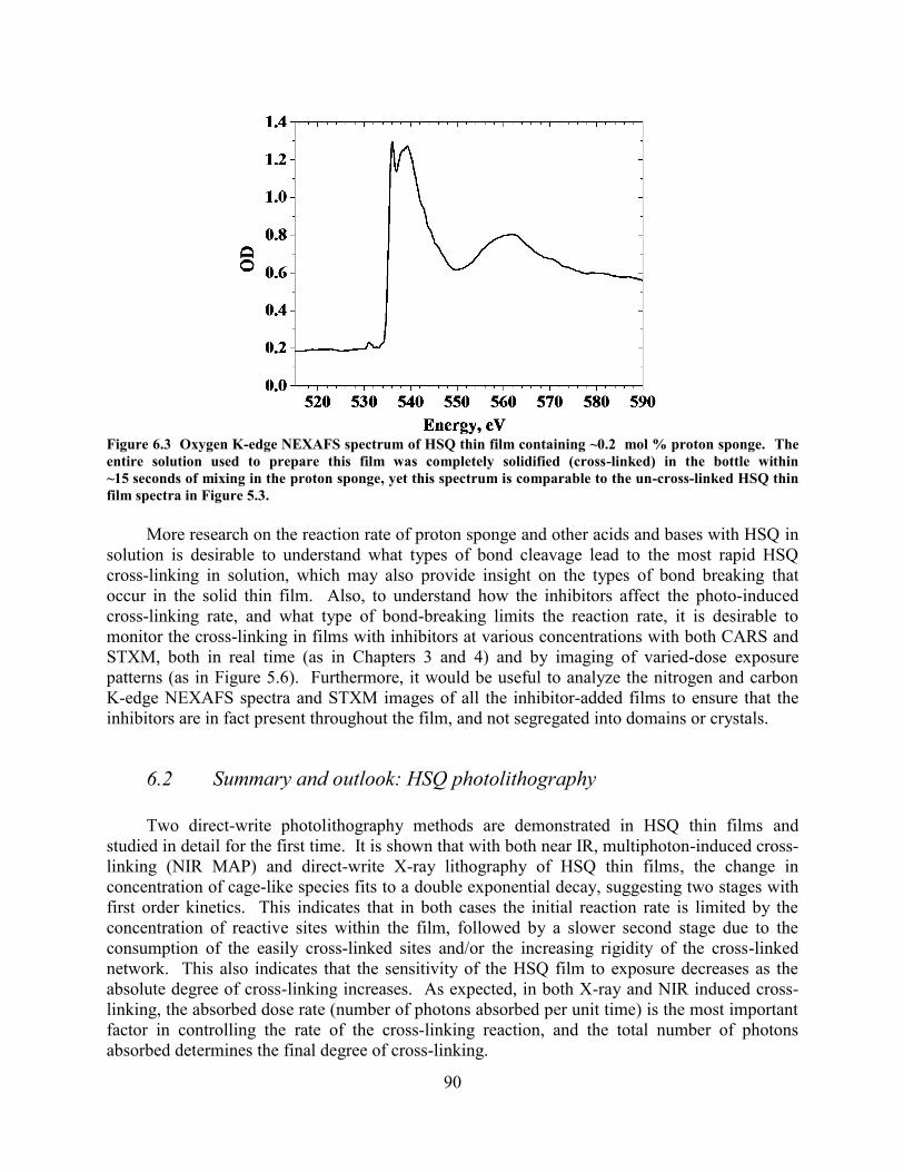
90
Figure 6.3 Oxygen K-edge NEXAFS spectrum of HSQ thin film containing ~0.2 mol % proton sponge. The
entire solution used to prepare this film was completely solidified (cross-linked) in the bottle within
~15 seconds of mixing in the proton sponge, yet this spectrum is comparable to the un-cross-linked HSQ thin
film spectra in Figure 5.3.
More research on the reaction rate of proton sponge and other acids and bases with HSQ in
solution is desirable to understand what types of bond cleavage lead to the most rapid HSQ
cross-linking in solution, which may also provide insight on the types of bond breaking that
occur in the solid thin film. Also, to understand how the inhibitors affect the photo-induced
cross-linking rate, and what type of bond-breaking limits the reaction rate, it is desirable to
monitor the cross-linking in films with inhibitors at various concentrations with both CARS and
STXM, both in real time (as in Chapters 3 and 4) and by imaging of varied-dose exposure
patterns (as in Figure 5.6). Furthermore, it would be useful to analyze the nitrogen and carbon
K-edge NEXAFS spectra and STXM images of all the inhibitor-added films to ensure that the
inhibitors are in fact present throughout the film, and not segregated into domains or crystals.
6.2 Summary and outlook: HSQ photolithography
Two direct-write photolithography methods are demonstrated in HSQ thin films and
studied in detail for the first time. It is shown that with both near IR, multiphoton-induced cross-
linking (NIR MAP) and direct-write Xray lithography of HSQ thin films, the change in
concentration of cage-like species fits to a double exponential decay, suggesting two stages with
first order kinetics. This indicates that in both cases the initial reaction rate is limited by the
concentration of reactive sites within the film, followed by a slower second stage due to the
consumption of the easily cross-linked sites and/or the increasing rigidity of the cross-linked
network. This also indicates that the sensitivity of the HSQ film to exposure decreases as the
absolute degree of cross-linking increases. As expected, in both X-ray and NIR induced cross-
linking, the absorbed dose rate (number of photons absorbed per unit time) is the most important
factor in controlling the rate of the cross-linking reaction, and the total number of photons
absorbed determines the final degree of cross-linking.

91
Some parallels can be drawn between the STXM and NIR MAP reaction mechanisms. The
oxygen K-edge NEXAFS spectra of the HSQ films show a clear increase in oxygen content
within the Xray cross-linked regions, caused by the absorption of additional water and/or
incorporation of additional oxygen atoms into the network structure with cross-linking. The first
stage of the multiphoton cross-linking is initiated by 6±1 near IR photons above a particular
power threshold of ~45 mW for ~38 fs pulses (before microscope), which equates to 9.4±2.2 eV
absorbed per cross-link. While not conclusive, both of these results are consistent with
previously proposed (but not confirmed) ebeam or high temperature reaction mechanisms
initiated by direct cleavage of two adjacent bonds, followed by the linking of two intact
HSQ monomer cages by an added oxygen (from atmospheric water or O2, equations 4.14 and
4.15). Several other possible mechanisms are also explored for the first stage of the
multiphoton-induced cross-linking, involving bond redistribution, and bond
scission, and it is possible that the Xray and NIR mechanisms are different. The presence and
potential role of a small initial concentration of on the cross-linking mechanism is also
considered for the first time in this work. Longer measurement times in NIR power dependence
studies are desired to assess the non-linearity of the second stage of the cross-linking mechanism,
and this comparison may also provide insight about the type of bond-breaking that initiates
cross-linking in each stage of the reaction
The NIR results suggest a different, possibly photothermal, mechanism for the very slow
cross-linking at low laser powers (less than ~45 mW for ~38 fs pulses), a regime not accessible
with previous methods used to study multiphoton ablation processes in positive tone resists.59
Assuming first order kinetics, a 10±3 photon process is indicated below threshold, with energy
deposition throughout the reactive site as opposed to direct photolytic bond breaking. However,
much longer measurement times are required to accurately assess the reaction order and power
dependence of this below-threshold cross-linking mechanism. Other studies of gaseous reaction
products (possibly via mass spectrometry) and cross-linking rates in different environments (e.g.
under very high vacuum to eliminate O2 and H2O) may also be helpful to narrow the possibilities
and pinpoint the precise X-ray and NIR induced conversion mechanisms, both above and below
the threshold.
After direct-write Xray lithography of HSQ, the high spatial resolution of the STXM
enables imaging of the spatial extent of the reaction with 30 nm resolution. In relatively thick
films (300-500 nm), reaction spread in excess of 70 nm on either side of the exposed region (at
the FWHM) is observed, which increases with dose and film thickness. The possibilities of
hydrogen radical migration or a proton initiated chain reaction causing the spread are explored in
detail, considering the observations in this study and several previous works. This spread is not
fully evident after development, as the developer washes away material below a relative degree
of cross-linking of approximately 7.5±2.5%. It is clear that this reaction spread can cause
significant proximity effects, including area dependent exposure sensitivity. The role of reaction
spread has been previously speculated in e-beam lithography of thinner HSQ films,8, 50
but the
STXM results shown here reveal the precise dose and thickness dependent extent of the
spreading effect in photolithography of these thicker films, prior to development. In future
studies, to achieve the minimum possible line widths, it is desirable to more precisely control the
film thickness, sample age, and delay between film preparation and exposure .
In this work, attempts to produce thin films of HSQ or MSQ from the pure, powdered
solids were not successful, as the solids will not dissolve appreciably in any commonly used
solvents (including those used for the commercial FOx HSQ solution), so some synthetic

92
modification of the starting materials is apparently necessary for thin film preparation. This
hypothesis was verified through discussions with several other photoresist experts, who stated
that must be incorporated into the HSQ (and MSQ) cage structure to improve solubility
for spin-on thin film application.132, 143-144, 178
To fully understand the cross-linking mechanism
of HSQ, and how to design similar resist materials, the concentration and role of in the
cross-linking mechanism should be determined. While NEXAFS and Raman spectra show
features that may be attributed to , there is a lack of concrete peak assignments
specifically for HSQ thin films. To enable more precise NEXAFS peak assignments for HSQ
thin films and related materials, more oxygen and silicon NEXAFS spectra of well-characterized,
substituted POSS molecules are desired, including samples with varied, known concentrations of
incorporated. In the Raman spectra, several potential bending modes overlap
other strong HSQ bands, but if a significant concentration of is present, more sensitive
Raman and/or FTIR spectroscopy of the ~3600-3900 cm-1
region should reveal a peak
corresponding to the stretching mode. Comparing the peak intensity to the
mode at ~2300 cm-1
for samples cross-linked by different methods may reveal the relative role of
the two types of bonds in the cross-linking reaction. Desired Raman spectra are, for example,
required for films cured at various temperatures, regions patterned with X-ray or NIR beam at
various doses, films made from fresh versus aged sample solution, and films in which there was
a varied delay between spin-coating or baking and exposure. Spectroscopy of the stock solution
may be useful, as well, but more likely will be complicated by the presence of the solvents
MIBK and toluene.
Another approach to assess the role of would be to synthesize the HSQ (and
substituted POSS) solutions from scratch, in order to have better control over the chemical
content of the starting materials, since the proprietary nature of the FOx® formulation of HSQ
prevents full disclosure by the manufacturer of the synthetic process and precise structure of
products in solution. Other standard characterization techniques, such as mass spectrometry,
NMR, or chromatography, may also be useful in assessing the concentration in
commercially available or custom made HSQ solutions and thin films. With current knowledge
and processing parameters, HSQ is not (yet) an ideal resist for commercial photolithography
applications, especially for integrated circuit manufacturing, due to its low sensitivity and delay
effects.2 However, understanding how and the overall HSQ cross-linking mechanism
affect the resist sensitivity, resolution and delay effects may be useful in designing modified
lithographic methods or new silicon-based photoresist materials for high-throughput
photolithography.
To date, the only other method demonstrated for following thin film polymerization
processes with relevant time resolution (< 1 second) is real-time FTIR spectroscopy (RTIR), and
this study expands the possibilities for solid thin films to include real-time monitoring of Raman
active modes. Compared to IR microscopy, broadband CARS microscopy also provides the
distinct advantage of imaging undeveloped, patterned resist thin films with sub-micron
resolution, demonstrated in other polymer films (PMMA and polystyrene, Figure 2.6), but not
yet in HSQ. For HSQ, a small degree of chirp on the laser pulse or sufficiently low laser power
effectively the halts cross-linking while maintaining a strong CARS signal, which should make it
possible to obtain images of patterned resists with little or no sample damage. This is also
expected to be true for any photoresist material that requires simultaneous absorption of >3 NIR
photons per cross-linking (or bond-breaking) event. This is analogous to STXM imaging, in

93
which fast scan rates and low photon flux are optimized to allow low-damage imaging even of
samples which are readily damaged by Xray exposure.
High resolution (sub-diffraction limited) multiphoton lithography using pulsed near IR
lasers has been applied to a variety of other photoresists, and this study opens the potential for
such patterning in HSQ and related POSS materials, as well. Features down to 120 nm wide
were patterned in 100 nm thick PMMA films with 170 fs pulses of 870 nm light at ~25 mW
average power, tightly focused with 1.3 NA, 100x objective, and it was determined that the
PMMA multiphoton bond-breaking and ablation were initiated by the absorption of 7±3
photons.59
The 6±1 photon non-linearity of the NIR MAP of HSQ observed in the present work
under comparable conditions indicates that a similar resolution enhancement may be expected in
HSQ, but development and AFM imaging of NIR patterns in HSQ are needed to verify the
lithographic resolution. The minimum line widths in HSQ are, of course, further limited by
reaction spread based on the HSQ film thickness, dose and delay effects, but the development
process can also be optimized to further enhance the feature resolution, as is the case for all HSQ
lithography.
In the future, this may enable the design and fabrication of 3D, multilevel microdevices
with pulsed NIR light in HSQ, and other silicon-based photoresists, with in situ CARS
characterization and monitoring. For reported multiphoton lithography of other materials,
typical point spacing of 100 nm and per-pixel dwell times from ~10 to 100 ms are utilized, so in
situ monitoring using CARS microscopy of these other processes may be feasible, as well. With
a relatively small addition of equipment to many of these current direct-write photolithography
setups, simultaneous patterning and monitoring of the degree of conversion (cross-linking or
bond breaking, for example in PMMA) could be achieved. The current sensitivity requires per-
pixel dwell times of at least 50 ms to achieve a useful CARS spectrum, but CARS sensitivity
improvements currently being developed may lower this dwell time limitation.115
Even the full
CARS setup, including pulse shaper, SLM, microscope, piezo stages and controllers, optics,
spectrometer and CCD, will likely cost less than an e-beam exposure apparatus, so it may be
preferable when >100 nm resolution features and in situ monitoring are desired. In fact, it may
be possible to even enhance multiphoton lithography rates in other polymers by using the pulse
shaping apparatus to compress the laser pulses, giving higher peak powers. A further advantage
of this setup is that the same microscope could be used for patterning and immediate post-pattern
imaging prior to development, similar to that demonstrated with the STXM microscope in
Chapter 5. In the future, there are other sensitive Raman microscopy techniques that may also be
utilized (with modification) for in situ monitoring and imaging of thin resist films, possibly
circumventing polarization issues encountered here and improving the temporal resolution of the
technique, such as FTSI-CARS131
and broadband stimulated Raman scattering (SRS).179-180
Even narrowband CARS has been used to assess the degree of cross-linking in polymer
photoresist structures after patterning,75, 142
so it is possible that a configuration for using
narrowband CARS or SRS181-182
for in situ monitoring during MAP patterning could also be
conceived. With the recent advances of MAP technology to sub-100 nm resolution,60
the
applications of this technique are expected to grow, and in situ monitoring may find an important
role in characterizing and optimizing the MAP materials and exposure methods. Regardless of
the techniques used, advances in HSQ and related photoresist materials are sure to play an
important role in the next generation of micro and nanolithography.

94
Bibliography
[1] Yang, J. K. W.; Cord, B.; Duan, H. G.; Berggren, K. K.; Klingfus, J.; Nam, S. W.; Kim,
K. B. and Rooks, M. J. J. Vac. Sci. Technol., B 2009, 27, 2622.
[2] Grigorescu, A. E. and Hagen, C. W. Nanotechnology 2009, 20, 292001.
[3] Reiser, A. Photoreactive Polymers: The Science and Technology of Resists; John Wiley
& Sons: New York, NY, 1989.
[4] Attwood, D. Soft X-Rays and Extreme Ultraviolet Radiation: Principles and
Applications; Cambridge University Press: New York, NY, 1999.
[5] The History of the Integrated Circuit,
http://nobelprize.org/educational_games/physics/integrated_circuit/history/ (January 1,
2010), The Official Web Site of the Nobel Foundation.
[6] Attwood, D., Errata: Soft X-rays and Extreme Ultraviolet Radiation,
http://ast.coe.berkeley.edu//sxreuv/errata.pdf (January 1, 2010).
[7] International Technology Roadmap for Semiconductors, http://www.itrs.net/reports.html
(January 1, 2010).
[8] Liddle, J. A.; Salmassi, F.; Naulleau, P. P. and Gullikson, E. M. J. Vac. Sci. Technol., B
2003, 21, 2980.
[9] Word, M. J.; Adesida, I. and Berger, P. R. J. Vac. Sci. Technol., B 2003, 21, L12.
[10] Attwood, D.; Chao, W. L.; Anderson, E.; Liddle, J. A.; Hartneck, B.; Fischer, P.;
Schneider, G.; Le Gros, M. and Larabell, C. J. Biomed. Nanotechnol. 2006, 2, 75.
[11] Chao, W.; Harteneck, B. D.; Liddle, J. A.; Anderson, E. H. and Attwood, D. T. Nature
2005, 435, 1210.
[12] Chao, W. L.; Kim, J.; Rekawa, S.; Fischer, P. and Anderson, E. J. Vac. Sci. Technol., B
2009, 27, 2606.
[13] Gil, D.; Menon, R. J. and Smith, H. I. J. Vac. Sci. Technol., B 2003, 21, 2956.
[14] Olynick, D. L.; Harteneck, B. D.; Veklerov, E.; Tendulkar, M.; Liddle, J. A.; Kilcoyne,
A. L. D. and Tyliszczak, T. J. Vac. Sci. Technol., B 2004, 22, 3186.
[15] Stade, F.; Heeren, A.; Fleischer, M. and Kern, D. P. Microelectron. Eng. 2007, 84, 1589.
[16] Weng, Y. J.; Weng, Y. C.; Fang, H. S. and Yang, S. Y. Jpn. J. Appl. Phys. 2009, 48.
[17] Arpin, K. A.; Mihi, A.; Johnson, H. T.; Baca, A. J.; Rogers, J. A.; Lewis, J. A. and Braun,
P. V. Adv. Mater. (Weinheim, Ger.) 2010, 22, 1084.
[18] Li, L. and Fourkas, J. T. Materials Today 2007, 10, 30.
[19] Blazej, R. G.; Kumaresan, P. and Mathies, R. A. Proc. Natl. Acad. Sci. U. S. A. 2006,
103, 7240.
[20] Jensen, E. C.; Bhat, B. P. and Mathies, R. A. Lab Chip 2010, 10, 685.
[21] Myers, F. B. and Lee, L. P. Lab Chip 2008, 8, 2015.
[22] Tsougeni, K.; Papageorgiou, D.; Tserepi, A. and Gogolides, E. Lab Chip 2010, 10, 462.
[23] Greener, J.; Li, W.; Ren, J.; Voicu, D.; Pakharenko, V.; Tang, T. and Kumacheva, E. Lab
Chip 2010, 10, 522.
[24] Jariwala, S.; Tan, B. and Venkatakrishnan, K. J. Michromech. Microeng. 2009, 19.
[25] Schafer, D.; Gibson, E. A.; Amir, W.; Erikson, R.; Lawrence, J.; Vestad, T.; Squier, J.;
Jimenez, R. and Marr, D. W. M. Opt. Lett. 2007, 32, 2568.
[26] Zhou, H.; Fang, G. J.; Yuan, L. Y.; Wang, C.; Yang, X. X.; Huang, H. H.; Zhou, C. H.
and Zhao, X. Z. Appl. Phys. Lett. 2009, 94.

95
[27] Gombert, A.; Blasi, B.; Buhler, C.; Nitz, P.; Mick, J.; Hossfeld, W. and Niggemann, M.
Opt. Eng. 2004, 43, 2525.
[28] Chen, C. P.; Tien, T. C.; Ko, B. T.; Chen, Y. D. and Ting, C. ACS Appl. Mater.
Interfaces 2009, 1, 741.
[29] McDonough, L. A. Microscopy and Spectroscopy of Water Uptake in Polymer
Photoresists. PhD Thesis, University of Colorado, Boulder, CO, 2004.
[30] Frye, C. L. and Collins, W. T. J. Am. Chem. Soc. 1970, 92, 5586.
[31] Loboda, M. J. and Toskey, G. A. Solid State Tech. 1998, 41, 99.
[32] Spin on Dielectrics,
http://www.dowcorning.com/content/etronics/etronicsspin/etronics_spin_imov.asp
(January 31, 2009), Dow Corning.
[33] Chang, T. C.; Chou, M. F.; Mei, Y. J.; Tsang, J. S.; Pan, F. M.; Wu, W. F.; Tsai, M. S.;
Chang, C. Y.; Shih, F. Y. and Huang, H. D. Thin Solid Films 1998, 332, 351.
[34] Liu, P. T.; Chang, T. C.; Tsai, T. M.; Lin, Z. W.; Chen, C. W.; Chen, B. C. and Sze, S. M.
Appl. Phys. Lett. 2003, 83, 4226.
[35] Loboda, M. J.; Grove, C. M. and Schneider, R. F. J. Electrochem. Soc. 1998, 145, 2861.
[36] Siew, Y. K.; Sarkar, G.; Hu, X.; Hui, J.; See, A. and Chua, C. T. J. Electrochem. Soc.
2000, 147, 335.
[37] Namatsu, H.; Takahashi, Y.; Yamazaki, K.; Yamaguchi, T.; Nagase, M. and Kurihara, K.
J. Vac. Sci. Technol., B 1998, 16, 69.
[38] Namatsu, H.; Yamaguchi, T.; Nagase, M.; Yamazaki, K. and Kurihara, K.
Microelectron. Eng. 1998, 42, 331.
[39] van Kan, J. A.; Zhang, F.; Zhang, C.; Bettiol, A. A. and Watt, F. Nucl. Instrum. Methods
Phys. Res., Sect. B 2008, 266, 1676.
[40] Sidorkin, V.; van Veldhoven, E.; van der Drift, E.; Alkemade, P.; Salemink, H. and
Maas, D. J. Vac. Sci. Technol., B 2009, 27, L18.
[41] Junarsa, I. P. and Nealey, P. F. J. Vac. Sci. Technol., B 2004, 22, 2685.
[42] Junarsa, I. P.; Stoykovich, M. P.; Nealey, P. F.; Ma, Y.; Cerrina, F. and Solak, H. H. J.
Vac. Sci. Technol., B 2005, 23, 138.
[43] Peuker, M.; Lim, M. H.; Smith, H. I.; Morton, R.; van Langen-Suurling, A. K.; Romijn,
J.; van der Drift, E. and van Delft, F. Microelectron. Eng. 2002, 61-2, 803.
[44] Guillorn, M.; Chang, J.; Fuller, N.; Patel, J.; Darnon, M.; Pyzyna, A.; Joseph, E.;
Engelmann, S.; Ott, J.; Newbury, J.; Klaus, D.; Bucchignano, J.; Joshi, P.; Scerbo, C.;
Kratschmer, E.; Graham, W.; To, B.; Parisi, J.; Zhang, Y. and Haensch, W. J. Vac. Sci.
Technol., B 2009, 27, 2588.
[45] Keil, K.; Choi, K. H.; Hohle, C.; Kretz, J.; Szikszai, L. and Bartha, J. W. J. Vac. Sci.
Technol., B 2009, 27, 47.
[46] Grigorescu, A. E.; Van der Krogt, M. C. and Hagen, C. W. J. Micro/Nanolithogr. MEMS
MOEMS 2007, 6.
[47] Haffner, M.; Haug, A.; Heeren, A.; Fleischer, M.; Peisert, H.; Chasse, T. and Kern, D. P.
J. Vac. Sci. Technol., B 2007, 25, 2045.
[48] van Delft, F. C. M. J. M. J. Vac. Sci. Technol., B 2002, 20, 2932.
[49] Clark, N.; Vanderslice, A.; Grove, R. and Krchnavek, R. R. J. Vac. Sci. Technol., B
2006, 24, 3073.
[50] Olynick, D. L.; Liddle, J. A.; Tivanski, A. V.; Gilles, M. K.; Tyliszczak, T.; Salmassi, F.;
Liang, K. and Leone, S. R. J. Vac. Sci. Technol., B 2006, 24, 3048.

96
[51] Grigorescu, A. E.; van der Krogt, M. C.; Hagen, C. W. and Kruit, P. J. Vac. Sci.
Technol., B 2007, 25, 1998.
[52] Grigorescu, A. E.; van der Krogt, M. C.; Hagen, C. W. and Kruit, P. Microelectron. Eng.
2007, 84, 822.
[53] Ekinci, Y.; Solak, H. H.; Padeste, C.; Gobrecht, J.; Stoykovich, M. P. and Nealey, P. F.
Microelectron. Eng. 2007, 84, 700.
[54] Chang, T. C.; Tsai, T. M.; Liu, P. T.; Mor, Y. S.; Chen, C. W.; Sheu, J. T. and Tsengb, T.
Y. Electrochem. Solid-State Lett. 2003, 6, G69.
[55] Zhu, X. L.; Xie, C. Q.; Zhang, M. H.; Liu, M.; Chen, B. Q. and Pan, F. Chin. Phys. Lett.
2009, 26, 086803.
[56] Tilley, D. University of California, Berkeley, CA. Personal communication, 2009.
[57] Liu, W. C.; Yang, C. C.; Chen, W. C.; Dai, B. T. and Tsai, M. S. J. Non-Cryst. Solids
2002, 311, 233.
[58] Yang, C. C. and Chen, W. C. J. Mater. Chem. 2002, 12, 1138.
[59] Ibrahim, S.; Higgins, D. A. and Ito, T. Langmuir 2007, 23, 12406.
[60] Li, L.; Gattass, R. R.; Gershgoren, E.; Hwang, H. and Fourkas, J. T. Science 2009, 324,
910.
[61] Kawata, S.; Sun, H.-B.; Tanaka, T. and Takada, K. Nature 2001, 412, 697.
[62] Sun, Z. B.; Dong, X. Z.; Chen, W. Q.; Nakanishi, S.; Duan, X. M. and Kawata, S. Adv.
Mater. (Weinheim, Ger.) 2008, 20, 914.
[63] Hanada, Y.; Sugioka, K.; Kawano, H.; Ishikawa, I. S.; Miyawaki, A. and Midorikawa, K.
Biomedical Microdevices 2008, 10, 403.
[64] Kumi, G.; Yanez, C. O.; Belfield, K. D. and Fourkas, J. T. Lab Chip 2010, 10, 1057.
[65] Baldacchini, T.; LaFratta, C. N.; Farrer, R. A.; Teich, M. C.; Saleh, B. E. A.; Naughton,
M. J. and Fourkas, J. T. J. Appl. Phys. 2004, 95, 6072.
[66] Chen, Y. F.; Yang, H. F. and Cui, Z. Microelectron. Eng. 2006, 83, 1119.
[67] Choi, S.; Jin, N.; Kumar, V.; Adesida, I. and Shannon, M. J. Vac. Sci. Technol., B 2007,
25, 2085.
[68] Tivanski, A.; Olynick, D. L.; Gilles, M. K. and Leone, S. R. (in preparation).
[69] Maker, P. D. and Tehrune, R. W. Phys. Rev. 1965, 137, A801.
[70] Roy, S.; Gord, J. R. and Patnaik, A. K. Progr. Energy Combust. Sci. 2010, 36, 280.
[71] Evans, C. L.; Potma, E. O.; Puoris'haag, M.; Côté, D.; Lin, C. P. and Xie, X. S. Proc.
Natl. Acad. Sci. U. S. A. 2005, 102, 16807.
[72] Henry, F. P.; Côté, D.; Randolph, M. A.; Rust, E. A. Z.; Redmond, R. W.; Kochevar, I.
E.; Lin, C. P. and Winograd, J. M. Plast. Reconstr. Surg. 2009, 123, 123S.
[73] Duncan, M. D.; Rientjes, J. and Manuccia, T. J. Opt. Lett. 1982, 7, 350.
[74] Zumbusch, A.; Holtom, G. R. and Xie, X. S. Phys. Rev. Lett. 1999, 82, 4142.
[75] Potma, E. O.; Xie, S. X.; Muntean, L.; Preusser, J.; Jones, D.; Ye, J.; Leone, S. R.;
Hinsberg, W. D. and Schade, W. J. Phys. Chem. B 2004, 108, 1296.
[76] Decker, C. Macromol. Rapid Commun. 2002, 23, 1067.
[77] Zhou, H.; Li, Q.; Lee, T. Y.; Guymon, A.; Jönsson, E. S. and Hoyle, C. E.
Macromolecules 2006, 39, 8269.
[78] Laskarakis, A.; Kassavetis, S.; Gravalidis, C. and Logothetidis, S. Nucl. Instrum.
Methods Phys. Res., Sect. B 2010, 268, 460.
[79] Caster, A. G.; Kowarik, S.; Schwartzberg, A. M.; Nicolet, O.; Lim, S. H. and Leone, S.
R. J. Raman Spectrosc. 2009, 40, 770.

97
[80] Muntean, L.; Planque, R.; Kilcoyne, A. L. D.; Leone, S. R.; Gilles, M. K. and Hinsberg,
W. D. J. Vac. Sci. Technol., B 2005, 21, 1630.
[81] Wang, J.; Stover, H. D. H. and Hitchcock, A. P. J. Phys. Chem. C 2009, 111, 16330.
[82] Wang, J.; Stover, H. D. H.; Hitchcock, A. P. and Tyliszczak, T. J. Synchrotron Radiat.
2007, 14, 181.
[83] Gilles, M. K. and Tivanski, A. Lawrence Berkeley National Laboratory, Berkeley, CA.
Unpublished work, 2005.
[84] Isoyan, A.; Wuest, A.; Wallace, J.; Jiang, F. and Cerrina, F. Opt. Express 2008, 16, 9106.
[85] Wachulak, P. W.; Capeluto, M. G.; Menoni, C. S.; Rocca, J. J. and Marconi, M. C. Opto-
Electron. Rev. 2008, 16, 444.
[86] Herzberg, G. Infrared and Raman Spectra of Polyatomic Molecules; D. Van Nostrand
Company, Inc.: New York, NY, 1945.
[87] Harvey, A. B. Anal. Chem. 1978, 50, A905.
[88] Lim, S. H.; Caster, A. G. and Leone, S. R. Phys. Rev. A 2005, 72.
[89] Lim, S. H.; Caster, A. G.; Nicolet, O. and Leone, S. R. J. Phys. Chem. B 2006, 110,
5196.
[90] Boyd, R. W. Nonlinear Optics, Third ed.; Elsevier: London, 2008.
[91] Yueh, F. Y. and Beiting, E. J. Comput. Phys. Commun. 1986, 42, 65.
[92] Chen, J. X.; Volkmer, A.; Book, L. D. and Xie, X. S. J. Phys. Chem. B 2002, 106, 8493.
[93] Wurpel, G. W. H.; Schins, J. M. and Muller, M. Opt. Lett. 2002, 27, 1093.
[94] Rinia, H. A.; Bonn, M. and Muller, M. J. Phys. Chem. B 2006, 110, 4472.
[95] Pestov, D.; Murawski, R. K.; Ariunbold, G. O.; Wang, X.; Zhi, M. C.; Sokolov, A. V.;
Sautenkov, V. A.; Rostovtsev, Y. V.; Dogariu, A.; Huang, Y. and Scully, M. O. Science
2007, 316, 265.
[96] Knutsen, K. P.; Messer, B. M.; Onorato, R. M. and Saykally, R. J. J. Phys. Chem. B
2006, 110, 5854.
[97] Andresen, E. R.; Paulsen, H. N.; Birkedal, V.; Thogersen, J. and Keiding, S. R. J. Opt.
Soc. Am. B 2005, 22, 1934.
[98] Pegoraro, A. F.; Ridsdale, A.; Moffatt, D. J.; Jia, Y. W.; Pezacki, J. P. and Stolow, A.
Opt. Express 2009, 17, 2984.
[99] Cheng, J. X.; Volkmer, A.; Book, L. D. and Xie, X. S. J. Phys. Chem. B 2002, 106,
8493.
[100] Evans, C. L.; Potma, E. O. and Xie, X. S. N. Opt. Lett. 2004, 29, 2923.
[101] Kee, T. W. and Cicerone, M. T. Opt. Lett. 2004, 29, 2701.
[102] Okuno, M.; Kano, H.; Leproux, P.; Couderc, V. and Hamaguchi, H. Opt. Lett. 2007, 32,
3050.
[103] Dudovich, N.; Oron, D. and Silberberg, Y. Nature 2002, 418, 512.
[104] Oron, D.; Dudovich, N. and Silberberg, Y. Phys. Rev. Lett. 2003, 90.
[105] Dudovich, N.; Oron, D. and Silberberg, Y. J. Chem. Phys. 2003, 118, 9208.
[106] Lepetit, L.; Cheriaux, G. and Joffre, M. J. Opt. Soc. Am. B 1995, 12, 2467.
[107] Caster, A. G.; Lim, S. H.; Nicolet, O. and Leone, S. R. Spectroscopy 2006, 21, 2.
[108] Lim, S. H. Lawrence Berkeley National Laboratory, Berkeley, CA. Lead researcher for
measurement and analysis of data in Figures 2.5 and 2.6, 2005.
[109] Potma, E. O.; Evans, C. L. and Xie, X. S. Opt. Lett. 2006, 31, 241.
[110] Caster, A. G.; Lim, S. H.; Nicolet, O. and Leone, S. R. Spectroscopy 2006, 21, 31.
[111] Johnson, W. C.; Wang, J. and Chen, Z. J. Phys. Chem. B 2005, 109, 6280.
98
[112] Wave plate, http://en.wikipedia.org/wiki/File:Waveplate.png (January 1, 2010),
Wikipedia. Figure used under terms of Creative Commons Attribution ShareAlike 3.0
License.
[113] Weiner, A. M. Rev. Sci. Instrum. 2000, 71, 1929.
[114] Lozovoy, V. V.; Pastkirk, I. and Dantus, M. Opt. Lett. 2004, 29, 1.
[115] Chen, B. C. and Lim, S. H. J. Phys. Chem. B 2008, 112, 3653.
[116] Stohr, J. NEXAFS Spectroscopy, Ertl, G., Gomer, R., Mills, D. L. et al., Eds.; Springer
Ser. Surf. Sci.; Springer-Verlag: Berlin, 1992.
[117] Brandes, J. A.; Lee, C.; Wakeham, S.; Peterson, M.; Jacobsen, C.; Wirick, S. and Cody,
G. Mar. Chem. 2004, 92, 107.
[118] Henke, B. L.; Gullikson, E. M. and Davis, J. C. At. Data Nucl. Data Tables 1993, 55,
349.
[119] Thompson, A. C.; Kirz, J.; Attwood, D. T.; Gullikson, E. M.; Howells, M. R.; Kortright,
J. B.; Liu, Y.; Robinson, A. R.; Underwood, J. H.; Kim, K. J.; Lindau, I.; Pianetta, P.;
Winick, H.; Williams, G. P. and Scofield, J. H. X-ray Data Booklet, Third ed.,
Thompson, A. C., Ed.; Lawrence Berkeley National Laboratory: Berkeley, CA, 2009.
[120] Kilcoyne, A. L. D.; Tyliszczak, T.; Steele, W. F.; Fakra, S.; Hitchcock, P.; Franck, K.;
Anderson, E.; Harteneck, B.; Rightor, E. G.; Mitchell, G. E.; Hitchcock, A. P.; Yang, L.;
Warwick, T. and Ade, H. J. Synchrotron Radiat. 2003, 10, 125.
[121] Bloomstein, T. M.; Juodawlkis, P. W.; Swint, R. B.; Cann, S. G.; Deneault, S. J.;
Efremow, N. N.; Hardy, D. E.; Marchant, M. F.; Napoleone, A.; Oakley, D. C. and
Rothschild, M. J. Vac. Sci. Technol., B 2005, 23, 2617.
[122] Wu, E.-S.; Strickler, J. H.; Harrell, W. R. and Webb, W. W., Cuthbert, J. D., Ed. (SPIE,
San Jose, CA, USA, 1992), vol. 1674, pp. 776-782.
[123] Zhou, W.; Kuebler, S. M.; Braun, K. L.; Yu, T.; Cammack, J. K.; Ober, C. K.; Perry, J.
W. and Marder, S. R. Science 2002, 296, 1106.
[124] Cumpston, B. H.; Ananthavel, S. P.; Barlow, S.; Dyer, D. L.; Ehrlich, J. E.; Erskine, L.
L.; Heikal, A. A.; Kuebler, S. M.; Lee, I. Y. S.; McCord-Maughon, D.; Qin, J. Q.;
Rockel, H.; Rumi, M.; Wu, X. L.; Marder, S. R. and Perry, J. W. Nature 1999, 398, 51.
[125] LaFratta, C. N.; Baldacchini, T.; Farrer, R. A.; Fourkas, J. T.; Teich, M. C.; Saleh, B. E.
A. and Naughton, M. J. J. Phys. Chem. B 2004, 108, 11256.
[126] Albrecht, M. G. and Blanchette, C. J. Electrochem. Soc. 1998, 145, 4019.
[127] Bornhauser, P. and Calzaferri, G. J. Phys. Chem. 1996, 100.
[128] Decker, C. Photo-induced Polymerization - Kinetic Study of Ultrafast Processes Induced
by UV Radiation or Lasers. In Photochemistry and Polymeric Systems; Kelly, J. M.,
McArdle, C. B. and Maunder, M. J. d. F., Eds.; The Royal Society of Chemistry:
Cambridge, UK, 1993; pp. 32-46.
[129] Belot, V.; Corriu, R.; Leclercq, D.; Mutin, P. H. and Vioux, A. Chem. Mater. 1991, 3,
127.
[130] Liou, H. C. and Pretzer, J. Thin Solid Films 1998, 335, 186.
[131] Lim, S. H.; Caster, A. G. and Leone, S. R. Opt. Lett. 2007, 32, 1332.
[132] Fleischer, M. Molecular Foundry, Lawrence Berkeley National Laboratory, Berkeley,
CA. Personal communication, 2009.
[133] Bornhauser, P. and Calzaferri, G. Spectrochim. Acta, Part A 1990, 46A, 1045.
[134] Ignatyev, I. S.; Partal, F.; Gonzalez, J. J. L. and Sundius, T. Spectrochim. Acta, Part A
2004, 60, 1169.

99
[135] Ogasawara, T.; Nara, A.; Okabayashi, E.; Nishio, E. and O'Connor, C. J. Colloid Polym.
Sci. 2000, 278, 1070.
[136] Morrow, B. A. and McFarlan, A. J. J. Phys. Chem. 1992, 96, 1395.
[137] Burneau, A. and Carteret, C. Phys. Chem. Chem. Phys. 2000, 2, 3217.
[138] Bertoluzza, A.; Fagnano, C. and Morelli, M. A. J. Non-Cryst. Solids 1982, 78, 117.
[139] Frost, R.; Cejka, J.; Weier, M. L. and Martens, W. J. Raman Spectrosc. 2006, 37, 538.
[140] LaFratta, C. N.; Fourkas, J. T.; Baldacchini, T. and Farrer, R. A. Angew. Chem., Int. Ed.
2007, 46, 6238.
[141] Higgins, D. A.; Everett, T. A.; Xie, A.; Forman, S. M. and Ito, T. Appl. Phys. Lett. 2006,
88, 184101(1.
[142] Baldacchini, T.; Zimmerley, M.; Kuo, C. H.; Potma, E. O. and Zadoyan, R. J. Phys.
Chem. B 2009, 113, 12663.
[143] Dubois, G. IBM Almaden Research Center, San Jose, CA. Personal communication,
2007.
[144] Olynick, D. Molecular Foundry, Lawrence Berkeley National Laboratory, Berkeley,CA.
Personal communication, 2009.
[145] Tyliszczak, T.; Warwick, T.; Kilcoyne, A. L. D.; Fakra, S.; Shuh, D. K.; Yoon, T. H.;
Brown, J., G. E.; Andrews, S.; Chembrolu, V.; Strachan, J. and Acremann, Y.
Synchrotron Radiation Instrumentation 2003 AIP Conference Proceedings 2004, 705,
1356.
[146] Heck, J. M.; Attwood, D.; Meyer-Ilse, W. and Anderson, E. H. J. X-ray Sci. Technol.
1998, 8, 95.
[147] Attwood, D. Lawrence Berkeley National Laboratory, Berkeley, CA. Personal
communication, 2010.
[148] Morrison, G. R.; Bridgwater, S.; Browne, M. T.; Burge, R. E.; Cave, R. C.;
Charalambous, P. S.; Foster, G. F.; Hare, A. R.; Michette, A. G.; Morris, D.; Taguchi, T.
and Duke, P. J. Rev. Sci. Instrum. 1989, 60, 2464.
[149] Bremmer, J. N.; Liu, Y.; Gruszynski, K. G. and Dali, F. C. Mater. Res. Soc. Symp. Proc.
1997, 476, 37.
[150] Gullikson, E. M., X-Ray Interactions With Matter, http://www.cxro.msd.lbl.gov/ (August
26, 2009).
[151] Yang, J. K. W. and Berggren, K. K. J. Vac. Sci. Technol., B 2007, 25, 2025.
[152] Tanaka, I.; Kawai, J. and Adachi, H. Phys. Rev. B 1995, 52, 11733.
[153] Brown Jr, G. E.; Waychunas , G. A.; Stohr, J. and Sette, F. Journal de Physique 1986,
47, C8 685
[154] Bubeck, R. A.; Dvornic, P. R.; Hu, J.; Hexemer, A.; Li, X.; Keinath, S. E. and Fischer, D.
A. Macromol. Chem. Phys. 2005, 206, 1146.
[155] Coulman, D.; Puschmann, A.; Hofer, U.; Steinruck, H. P.; Wurth, W.; Feulner, P. and
Menzel, D. J. Chem. Phys. 1990, 93, 58.
[156] Pangher, N.; Schmalz, A. and Haase, J. Chem. Phys. Lett. 1994, 221, 189.
[157] Zhao, J. H.; Malik, I.; Ryan, T.; Ogawa, E. T. and Ho, P. S. Appl. Phys. Lett. 1999, 74,
944.
[158] Lin, L. W.; Tang, Y. H.; Li, X. X.; Pei, L. Z.; Zhange, Y. and Guo, C. J. Appl. Phys.
2007, 101, 014314 1.
[159] Malaske, U.; Pfnur, H.; Bassler, M.; Weiss, M. and Umbach, E. Phys. Rev. B 1996, 53,
13115.

100
[160] Bayliss, S. C.; Zhang, Q. and Hutt, D. A. Physics and Statistics of Solids 1995, 190, 85.
[161] Friedman, S. L.; Marcus, M. A.; Adler, D. L.; Xie, Y.-H.; Harris, T. D. and Citrin, P. H.
Mater. Res. Soc. Symp. Proc. 1993, 298, 295.
[162] Bayliss, S. C.; Anstee, P.; Hutt, D. A.; Zhang, Q.; Danson, N.; Bates, J. and Waddilove,
A. J. Appl. Phys. 1994, 76, 5171.
[163] Hessel, C. M.; Henderson, E. J.; Kelly, J. A.; Cavell, R. G.; Sham, T. K. and Veinot, J. G.
C. J. Phys. Chem. C 2008, 112, 14247.
[164] Henschel, W.; Georgiev, Y. M. and Kurz, H. J. Vac. Sci. Technol., B 2003, 21, 2018.
[165] Sidorkin, V.; Grigorescu, A. E.; Salemink, H. and van der Drift, E. Microelectron. Eng.
2009, 86, 749.
[166] Nam, S. W.; Rooks, M. J.; Yang, J. K. W.; Berggren, K. K.; Kim, H. M.; Lee, M. H.;
Kim, K. B.; Sim, J. H. and Yoon, D. Y. J. Vac. Sci. Technol., B 2009, 27, 2635.
[167] Lee, C. W.; Ikematsu, Y. and Shindo, D. J. Electron Microsc. 2002, 51, 143.
[168] Tanuma, S.; Powell, C. J. and Penn, D. R. Surf. Interface Anal. 1993, 21, 165.
[169] Yamazaki, K. and Namatsu, H. Jpn. J. Appl. Phys., Part 1 2004, 43, 3767.
[170] Pach, M. and Stosser, R. J. Phys. Chem. A 1997, 101, 8360.
[171] Sasamori, R.; Okaue, Y.; Isobe, T. and Matsuda, Y. Science 1994, 265, 1691.
[172] Charlesby, A. and Garratt, P. G. Proc. R. Soc. London, A 1963, 273, 117.
[173] Olynick, D. L. et al. submitted 2010.
[174] Charlesby, A. Rep. Prog. Phys. 1965, 28, 463.
[175] Tivanski, A. The University of Iowa, Iowa City, IA. Personal communication, 2010.
[176] Daiko, Y.; Kasuga, T. and Nogami, M. Microporous Mesoporous Mater. 2004, 69, 149.
[177] Shkrob, I. A. and Trifunac, A. D. Phys. Rev. B 1996, 54, 15073.
[178] Techneglas, Inc., Perrysburg, OH. Personal communication, 2008.
[179] McCamant, D. W.; Kukura, P.; Yoon, S. and Mathies, R. A. Rev. Sci. Instrum. 2004, 75,
4971.
[180] Ploetz, E.; Laimgruber, S.; Berner, S.; Zinth, W. and Gilch, P. Appl. Phys. B: Lasers
Opt. 2007, 87, 389.
[181] Freudiger, C. W.; Min, W.; Saar, B. G.; Lu, S.; Holtom, G. R.; He, C. W.; Tsai, J. C.;
Kang, J. X. and Xie, X. S. Science 2008, 322, 1857.
[182] Nandakumar, P.; Kovalev, A. and Volkmer, A. New Journal of Physics 2009, 11.


![Lecture8-Photoresists and Nonoptical Lithography.ppt · 2018-01-05 · Microsoft PowerPoint - Lecture8-Photoresists and Nonoptical Lithography.ppt [Compatibility Mode] Author: Alan](https://static.fdocuments.net/doc/165x107/5f39b5e2fc77d34ccb580f41/lecture8-photoresists-and-nonoptical-2018-01-05-microsoft-powerpoint-lecture8-photoresists.jpg)


![COUNTERMEASURES AGAINST ANTI-RADIATION MISSILES S% … · 2011. 5. 14. · principle of investigating ARM [anti-radiation missile] with coherent or noncoherent dual-sources (quasi-dual-source).](https://static.fdocuments.net/doc/165x107/60655164019a2616922831f9/countermeasures-against-anti-radiation-missiles-s-2011-5-14-principle-of-investigating.jpg)
