Signal Chain Design Guide
34
www.microchip.com www.microchip.com/analogtools Analog & Interface Solutions Fall 2012 Signal Chain Design Guide Devices For Use With Sensors Design ideas in this guide use the following devices. A complete device list and corresponding data sheets for these products can be found at www.microchip.com/analog. Operational Amplifiers Instrumentation Amplifiers Comparators Analog-to-Digital Converters Digital Potentiometers Digital-to-Analog Converters Voltage References Temperature Sensors MCP6XX MCP6XXX MCP6VXX MCP6HXX MCP6NXX MCP654X MCP656X MCP65R4X MCP30XX MCP32XX MCP33XX MCP34XX MCP35XX MCP39XX MCP40XX MCP40D1X MCP41XX MCP42XX MCP43XX MCP45XX MCP46XX MCP41XXX MCP42XXX MCP47XX MCP48XX MCP49XX MCP47DA1 MCP47A1 TC132X MCP1525 MCP1541 MCP98XX MCP9700/A MCP9701/A
Transcript of Signal Chain Design Guide
www.microchip.comwww.microchip.com/analogtools
Analog & Interface Solutions
Fall 2012
Signal Chain Design GuideDevices For Use With Sensors
Design ideas in this guide use the following devices. A complete device list and corresponding data sheets for these products can be found at www.microchip.com/analog.
Operational Amplifiers
Instrumentation Amplifiers
Comparators Analog-to-Digital Converters
Digital Potentiometers
Digital-to-Analog Converters
Voltage References
Temperature Sensors
MCP6XXMCP6XXXMCP6VXXMCP6HXX
MCP6NXX MCP654XMCP656XMCP65R4X
MCP30XXMCP32XXMCP33XXMCP34XXMCP35XXMCP39XX
MCP40XXMCP40D1XMCP41XXMCP42XXMCP43XXMCP45XXMCP46XXMCP41XXXMCP42XXX
MCP47XXMCP48XXMCP49XXMCP47DA1MCP47A1TC132X
MCP1525MCP1541
MCP98XXMCP9700/AMCP9701/A
2 Signal Chain Design Guide
Signal Chain Overview
Typical Sensor Signal Chain Control Loop
Digital DomainAnalog Domain
Driver(MOSFET)
Op AmpDAC/PWM
Actuators
Motors, Valves,Relays, Switches,Speakers, Horns,
LEDs
ADC/V-to-Freq
Amp
Sensors
Filter
ReferenceVoltage
MUX
PIC® MCU or dsPIC®
DSC
Indicator(LCD, LED)
DigitalPotentiometer
Typical sensor applications involve the monitoring of sensor parameters and controlling of actuators. The sensor signal chain, as shown below, consists of analog and digital domains. Typical sensors output very low amplitude analog signals. These weak analog signals are amplified and filtered, and converted to digital values using op amps, analog-to-digital or voltage-to-frequency converters, and are processed at the MCU. The analog sensor output typically needs proper signal conditioning before it gets converted to a digital signal.
The MCU controls the actuators and maintains the operation of the sensor signal conditioning circuits based on the condition of the signal detection. In the digital to analog feedback path, the digital-to-analog converter (DAC), digital potentiometer and Pulse-Width-Modulator (PWM) devices are most commonly used. The MOSFET driver is commonly used for the interface between the feedback circuit and actuators such as motors and valves. Microchip offers a large portfolio of devices for signal chain applications.
3Signal Chain Design Guide
Many system applications require the measurement of a physical or electrical condition, or the presence or absence of a known physical, electrical or chemical quantity. Analog sensors are typically used to indicate the magnitude or change in the environmental condition, by reacting to the condition and generating a change in an electrical property as a result.
Typical phenomena that are measured are: Electrical signal and properties Magnetic signal and properties Temperature Humidity Force, weight, torque and pressure Motion and vibration Flow Fluid level and volume Light and infrared Chemistry/gas
Summary Of Common Physical Conditions and Related Sensor Types
Phenomena Sensor Electrical Output
MagneticHall Effect VoltageMagneto-Resistive Resistance
Temperature
Thermocouple VoltageRTD ResistanceThermistor ResistanceIC VoltageInfrared Current
HumidityCapacitive CapacitanceInfrared Current
Force, Weight, Torque, Pressure
Strain Gauge Resistance/VoltageLoad Cell ResistancePiezoelectric Voltage or ChargeMechanical Transducer Resistance, Voltage, Capacitance
Motion and Vibration
LVDT AC VoltagePiezoelectric Voltage or ChargeMicrophone VoltageUltrosonic Voltage, Resistive, CurrentAccelerometer Voltage
Flow
Magnetic Flowmeter VoltageMass Flowmeter Resistance/VoltageUltrasound/Doppler FrequencyHot-wire Anemometer ResistanceMechanical Transducer (turbine) Voltage
Fluid Level and Volume
Ultrasound Time DelayMechanical Transducer Resistance/VoltageCapacitor CapacitanceSwitch On/OffThermal Voltage
TouchCapacitance VoltageInductance CurrentResistance Frequency
ProximityCapacitance Voltage, FrequencyInductance Current, FrequencyResistance Voltage, Current
Light Photodiode Current
Chemical
pH Electrode VoltageSolution Conductivity Resistance/CurrentCO Sensor Voltage or ChargePhotodiode (turbidity, colorimeter) CurrentIon Sensor Current
Sensor OverviewThere are sensors that respond to these phenomena by producing the following electrical properties:
Voltage Current Resistance Capacitance Charge
This electrical property is then conditioned by an analog circuit before being driven to a digital circuit. In this way, the environmental condition can be “measured” and the system can make decisions based on the result.
The table below provides an overview of typical phenomena, the type of sensor commonly used to measure the phenomena and electrical output of the sensor.
For additional information, please refer to Application Note AN990.
4 Signal Chain Design Guide
Operational Amplifiers (Op Amps)Microchip Technology offers a broad portfolio of op amp families built on advanced CMOS technology. These families are offered in single, dual and quad configurations, which are available in space saving packages.
These op amp families include devices with Quiescent Current (Iq) per amplifier between 0.45 µA and 6 mA, with a Gain Bandwidth Product (GBWP) between 9 kHz and 60 MHz, respectively. The op amp with lowest supply voltage (Vdd) operates between 1.4V and 6.0V, while the op amp with highest Vdd operates between 6.5V and 16.0V.
These op amp families fall into the following categories: General Purpose, Precision (including EPROM Trimmed and mCal Technology) and Zero-Drift.
Instrumentation Amplifiers (INA)Microchip has expanded its portfolio of amplifiers with the industry’s first instrumentation amplifier featuring mCal technology. The MCP6N11 features rail-to-rail input and output, 1.8V operation and low offset/offset drift.
ComparatorsMicrochip offers a broad portfolio of low-power and high-speed comparators. The MCP6541 and MCP6561 family of comparators provide ultra low power, 600 nA typical, and higher speed with 40 ns propagation delay, respectively. Both families of comparators are available with single, dual and quad, as well as with push-pull and open-drain output options (for MCP6546 and MCP6566).The MCP65R41 and MCP65R46 family of push-pull and open-drain output comparators are offered with integrated reference voltages of 1.21V and 2.4V receptively. This family provides ±1% typical tolerance while consuming 2.5 μA and high speed with 4μs propagation delay. These comparators operate with a single-supply voltage as low as 1.8V to 5.5V, which makes them ideal for low cost and/or battery powered applications.
Product Overviews
Programmable Gain Amplifier (PGA)The MCP6S21/2/6/8 and MCP6S91/2/3 PGA families give the designer digital control over an amplifier using a serial interface (SPI bus). An input analog multiplexer with 1, 2, 6 or 8 inputs can be set to the desired input signal. The gain can be set to one of eight non-inverting gains: + 1, 2, 4, 5, 8, 10, 16 and 32 V/V. In addition, a software shutdown mode offers significant power savings for portable embedded designs. This is all achieved in one simple integrated part that allows for considerably greater bandwidth, while maintaining a low supply current. Systems with multiple sensors are significantly simplified.
The MCP6G01 family are analog Selectable Gain Amplifiers (SGA). The Gain Select input pin(s) set a gain of + 1 V/V, +10 V/V and + 50 V/V. The Chip Select pin on the MCP6G03 puts it into shutdown to conserve power.
Analog-to-Digital Converters (ADC)Microchip offers a broad portfolio of high-precision Delta-Sigma, SAR and Dual Slope A/D Converters. The MCP3550/1/3 Delta-Sigma ADCs offer up to 22-bit resolution with only 120 μA typical current consumption in a small 8-pin MSOP package. The MCP3421 is a single channel 18-bit Delta-Sigma ADC and is available in a small 6-pin SOT-23 package. It includes a voltage reference and PGA. The user can select the conversion resolution up to 18 bits. The MCP3422/3 and the MCP3424 are two channel and four channel versions, respectively, of the MCP3421 device. The MCP300X (10-bit), MCP320X (12-bit) and MCP330X (13-bit) SAR ADCs combine high performance and low power consumption in a small package, making them ideal for embedded control applications. The MCP3911 analog front end offer two simultaneously sampled 24-bit Delta-Sigma ADCs making it ideal for voltage and current measurement, and other data acquisition applications.
The “Analog-to-Digital Converter Design Guide” (Microchip Document No. 21841) shows various application examples of the ADC devices.
Microchip also offers many high accuracy energy metering devices which are based on the Delta-Sigma ADC cores. The “Complete Utility Metering Solution Guide” (Microchip Document No: 24930) offers detailed solutions for metering applications.
5Signal Chain Design Guide
Voltage ReferencesMicrochip offers the MCP15XX family of low power and low dropout precision Voltage References. The family includes the MCP1525 with an output voltage of 2.5V and the MCP1541 with an output voltage of 4.096V. Microchip’s voltage references are offered in SOT23-3 and TO-92 packages.
Temperature SensorsMicrochip offers a broad portfolio of thermal management products, including Logic Output, Voltage Output and Serial Output temperature sensors. These products allow the system designer to implement the device that best meets the application requirements. Key features include high accuracy (such as MCP9808, with ±0.5°C maximum accuracy from −20°C to 100°C), low power, extended temperature range and small packages. In addition, other Microchip products can be used to support Thermocouple, RTD and Thermistor applications.
Digital PotentiometersMicrochip’s family of digital potentiometers offer a wide range of options. These devices support the 6-bit through 8-bit applications. Offering both volatile and non-volatile options, with digital interfaces from the simple Up/Down interface to the standard SPI and I2C™ interfaces. These devices are offered in small packages such as 6-lead SC70 and 8-lead DFN for the single potentiometer devices, 14-lead TSSOP and 16-lead QFN packages for the dual potentiometer devices, and 20-lead TSSOP and QFN packages for the quad potentiometer devices. Non-volatile devices offer a Wiperlock™ Technology feature, while volatile devices will operate down to 1.8V. Resistances are offered from 2.1 kΩ to 100 kΩ. Over 50 device configurations are currently available.
The “Digital Potentiometer Design Guide” (Microchip Document No. 22017), shows various application examples of the digital potentiometer devices.
Product Overviews
Digital-to-Analog Converters (DAC)Microchip’s family of Digital-to-Analog Converters (DACs) offer a wide range of options. These devices support the 6-bit through 12-bit applications. Offering both volatile and non-volatile options, and standard SPI and I2C digital interfaces. These devices are offered in small packages such as 6-lead SC70, SOT-23 and DFN (2 × 2) for the single output devices and 10-pin MSOP for quad output devices. Some versions support selecting either the device Vdd, the external voltage reference or an internally generated voltage reference source from the DAC circuitry. Devices with nonvolatile memory (EEPROM) allow the device to retain the programmed output code and DAC state through power down events.
These DAC devices provide high accuracy and low noise and are ideal for industrial applications where calibration or compensation of signals (such as temperature, pressure or humidity) is required.
6 Signal Chain Design Guide
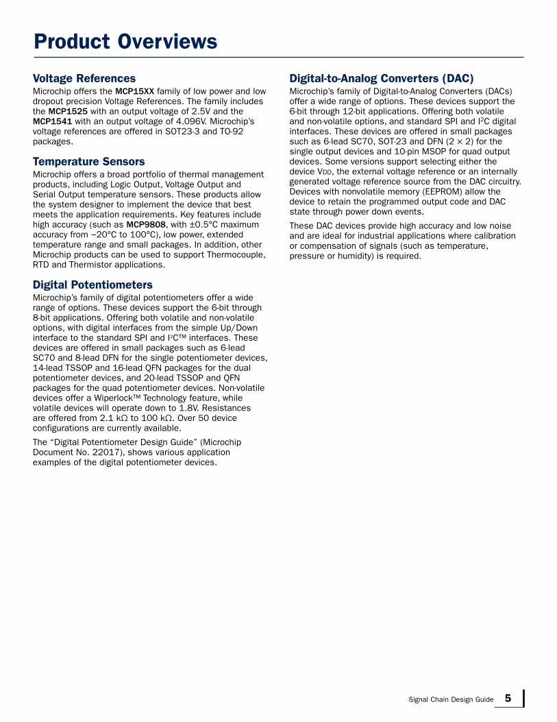
Local SensingLocal sensors are located relatively close to their signal conditioning circuits, and the noise environment is not severe; most of these sensors are single ended (not differential). Non-inverting amplifiers are a good choice for amplifying most of these sensors’ output because they have high input impedance, and require a minimal amount of discrete components.
Key Amplifier Features Low cost• General purpose op amps
High precision• Low offset op amps• Zero-drift op amps• Low noise op amps
Rail-to-rail input/output• Most op amp families
High input impedance• Op amps with CMOS inputs
Low power and portable applications• Low power op amps
High voltage• High voltage op amps
High bandwidth and slew rate• High speed op amps
Load drive• High output drive op amps
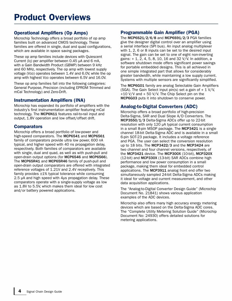
Classic Gain Amplifier
High Side Current Sensing Amplifier
+
pH Monitor
VOUT
MCP6XX,MCP6XXX
-
–
+
RSEN ISEN
R1 R2
VOUT
VREF
R1 R2
V1
V2
–
+
MCP6HXX
VDD
RSEN << R1, R2
VOUT = (V1 – V2) + VREFR2
R1( )
Local Sensors
Sensors and ApplicationsSingle Sensors
Thermistors for battery chargers and power supply temperature protection
Humidity Sensors for process control Pyroelectric infrared intrusion alarms, motion detection
and garage door openers Smoke and fire sensors for home and office Charge amplifier for Piezoelectric Transducer detection Thermistor for battery chargers and home thermostats LVDT position and rotation sensors for industrial control Hall effect sensors for engine speed sensing and
door openers Photoelectric infrared detector Photoelectric motion detectors, flame detectors,
intrusion alarms Sensing resistor for current detection
Multiple Local Sensors Temperature measurement at multiple points on a Printed
Circuit Board (PCB) Sensors that require temperature correction Weather measurements (temperature, pressure,
humidity, light)
Capacitive Humidity Sensor Circuit (PIC16F690DM-PCTLHS)
PIC16F690
MCP6291
VDD_DIGC1
U1
P4
100 nF
VCM
VDD
VSEN
VINT
RINT6.65 MΩ
CSEN
IINT
RCM120 kΩ
RCM220 kΩ
CCM100 nF
100 nF
CCG
C2
P3
P1
P2
U2–
+Comparator
VREF
SRLatch
Timer1
7Signal Chain Design Guide
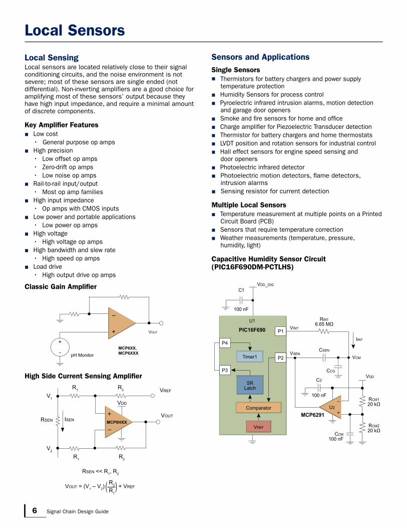
Remote SensingAll sensors in a high noise environment should be considered as remote sensors. Also, sensors not located on the same PCB as the signal conditioning circuitry are remote. Remote sensing applications typically use a differential amplifier or an instrumentation amplifier.
Key Amplifier Features Differential input Large CMR Small Vos
Products High Precision• Low Offset Op Amps• Auto-zeroed Op Amps• Low Noise Op Amps
Sensors and Applications High temperature sensors• Thermocouples for stoves, engines and process
control• RTDs for ovens and process control
Wheatstone Bridges• Pressure sensors for automotive and industrial
control• Strain gauges for engines
Low side current monitors for motors and batteries
Differential Amplifier
Thermocouple Circuit Using an INA
VOUT
EMI
EMI
VREF
MCP6VXX MCP616
–
+
TCJ
(Cold Junction)
InputFilter
Temp. Sensor
THJ
(Hot Junction)INA
–
+
–
+ADC
MCUVREF
2
2
Remote Sensors
8 Signal Chain Design Guide
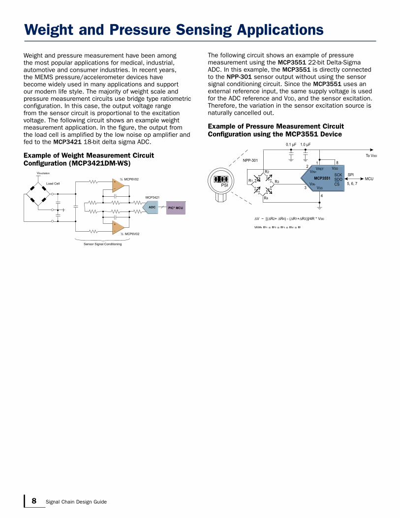
Weight and pressure measurement have been among the most popular applications for medical, industrial, automotive and consumer industries. In recent years, the MEMS pressure/accelerometer devices have become widely used in many applications and support our modern life style. The majority of weight scale and pressure measurement circuits use bridge type ratiometric configuration. In this case, the output voltage range from the sensor circuit is proportional to the excitation voltage. The following circuit shows an example weight measurement application. In the figure, the output from the load cell is amplified by the low noise op amplifier and fed to the MCP3421 18-bit delta sigma ADC.
Example of Weight Measurement Circuit Configuration (MCP3421DM-WS)
MCP3421
PIC® MCU
–
+
–
+
ADC
½ MCP6V02
½ MCP6V02
VExcitation
Load Cell
Sensor Signal Conditioning
Weight and Pressure Sensing ApplicationsThe following circuit shows an example of pressure measurement using the MCP3551 22-bit Delta-Sigma ADC. In this example, the MCP3551 is directly connected to the NPP-301 sensor output without using the sensor signal conditioning circuit. Since the MCP3551 uses an external reference input, the same supply voltage is used for the ADC reference and Vdd, and the sensor excitation. Therefore, the variation in the sensor excitation source is naturally cancelled out.
Example of Pressure Measurement Circuit Configuration using the MCP3551 Device
R2SPI
VREF
SCKSDOCS
MCP35515, 6, 7
12
3
4
8
VSS
VIN+
VIN-
To VDD
VDD
0.1 µF 1.0 µF
NPP-301
R1
R4
R3MCU
∆V ~ [(∆R2+ ∆R4) - (∆R1+∆R3)]/4R * VDD
With R1 = R2 = R3 = R4 = R
0.00PSI

9Signal Chain Design Guide
DC Voltage and Current MeasurementDC voltage and current measurement can be easily done by using low speed high resolution Delta Sigma ADC such as MCP3421 and MCP3422 family devices. The MCP3421 is a single channel device while the MCP3422 is a dual channel device, which can measure the voltage and current using the same device.
The following circuits show simple example of Battery voltage and current measurement using the MCP3421. The MCP3421 uses internal reference voltage of 2.048V. If the input voltage is greater than the reference, it needs a voltage divider to bring down the input full scale range below the reference voltage. This example is shown in example circuit (a). In the current measurement, the ADC is simply connected across a simple shunt current sensor as shown in the figure. The current is calculated using the measured voltage value and a known shunt’s resistance value. The MCP3421 has a differential input and the MSb in the output bit represents the direction of the current.
Voltage Measurement Using MCP3421 Device
Current Measurement Using MCP3421 Device
(a) If VREF < VBAT
ADCVBAT –
+
R2
R1
(b) If VREF > VBAT
R2VIN = ( ________ ) (VBAT)R1 + R2
R2VMeasured = ADC Output Codes LSB _________ _____(R1 + R2)PGA
1
2N–1LSB = ________________Reference Voltage
2.048V2172N–1LSB of 18-bit ADC = ________________ = ______ = 15.625 µV Reference Voltage
ADCVBAT
–
+
MCP3421MCP3421
MCU MCU
VIN
Current = (Measured Voltage)/(Known Resistance Value of Current Sensor)Direction of current is determined by sign bit (Msb bit) of the ADC output code.
ADCBattery
ChargingCurrent
DischargingCurrent
Current Sensor To Load
–+
MCP3421
MCU
Voltage and Current Measurement
Battery Fuel Management by Measuring Battery Voltage and CurrentBy measuring the battery voltage and current, an intelligent battery fuel management algorithm can be developed. The figure below shows an example of battery fuel management circuit. The MCP3422 measures both voltage and current draws of the battery, and the system tracks how much the battery fuel has been used and remained. The MCU controls the MCP73831 for the recharging of the single cell Li-Ion battery
Example Circuit for Battery Fuel Management by measuring Battery Voltage and Current
Batte
ry
MCU
MCP73831
MCP3422
CH B
R2
CH A
Charging Current
Decharging Current
Battery Fuel Measurement
Battery Fuel Charger
VBATS2
S1R1
STAT PROG
R3
Load
10 Signal Chain Design Guide
Voltage and Current Measurement
Example of Three-Phase Current and Voltage Measurement Using the MCP3911 Energy Metering Delta-Sigma ADC
Current Measurement Using Rogowski Coil
PIC24FJ256GA110Family
Flash128–256 kB
ADC10-bit16 ch
RAM16 kB
UARTUARTUARTUART
RTCC
32 KHz
RS485PLCIrDA®
RS485
I2C™
SPI Smart CardReader
PrepaymentCard
EEPROMGPIO
SPI
LCD Driver LCD Panel
NTC Thermistor
Battery
MCP3911
CurrentSampling
VoltageSampling
×3
Low VoltageDetect
Power Supply
Load
~ AC
Shunt
R2
I(t)
1
R1
C1
ADC
VDD
VOUT
2VIN
B-Field
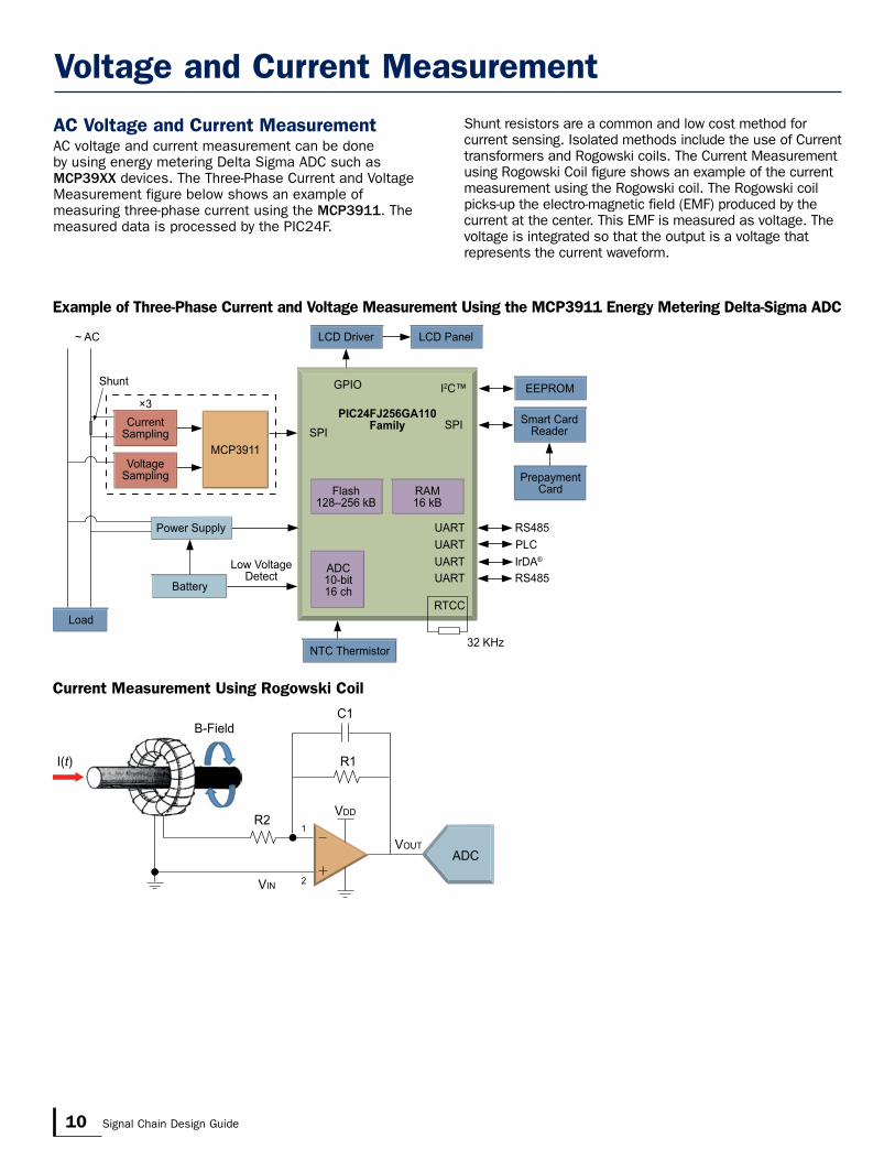
AC Voltage and Current MeasurementAC voltage and current measurement can be done by using energy metering Delta Sigma ADC such as MCP39XX devices. The Three-Phase Current and Voltage Measurement figure below shows an example of measuring three-phase current using the MCP3911. The measured data is processed by the PIC24F.
Shunt resistors are a common and low cost method for current sensing. Isolated methods include the use of Current transformers and Rogowski coils. The Current Measurement using Rogowski Coil figure shows an example of the current measurement using the Rogowski coil. The Rogowski coil picks-up the electro-magnetic field (EMF) produced by the current at the center. This EMF is measured as voltage. The voltage is integrated so that the output is a voltage that represents the current waveform.
11Signal Chain Design Guide
Temperature Sensing Solutions
Thermistor SolutionThermistors are non-linear and require a look up table for compensation. The solution is to use Microchip’s Linear Active Thermistors, the MCP9700 and the MCP9701. These are low-cost voltage output temperature sensors that replace almost any Thermistor application solutions. Unlike resistive type sensors such as Thermistors, the signal conditioning at the non-linear region and noise immunity circuit development overhead can be avoided by using the low-cost Linear Active Thermistors. The voltage output pin (Vout) can be directly connected to the ADC input of a microcontroller. The MCP9700/9700A and MCP9701/9701A temperature coefficients are scaled to provide a 1°C/bit resolution for an 8-bit ADC with a reference voltage of 2.5V and 5V, respectively.The MCP9700 and MCP9701 sensors output can be compensated for improved sensor accuracy as shown below, refer to the AN1001 application note.
MCP9700 and MCP9701 Key Features SC70, TO92 packages Operating temperature range: −40°C to +150°C Temperature Coeffi cient: 10 mV/°C (MCP9700) Temperature Coeffi cient: 19.5 mV/°C (MCP9701) Low power: 6 μA (typ.)
Applications Refrigeration equipment Power supply over temperature protection General purpose temperature monitoring
Typical Sensor Accuracy Before and After Compensation
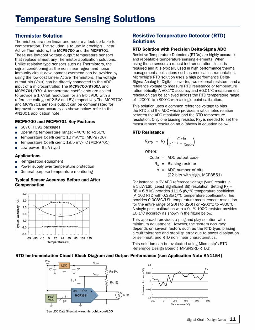
Resistive Temperature Detector (RTD) SolutionsRTD Solution with Precision Delta-Sigma ADCResistive Temperature Detectors (RTDs) are highly accurate and repeatable temperature sensing elements. When using these sensors a robust instrumentation circuit is required and it is typically used in high performance thermal management applications such as medical instrumentation. Microchip’s RTD solution uses a high performance Delta-Sigma Analog to Digital converter, two external resistors, and a reference voltage to measure RTD resistance or temperature ratiometrically. A ±0.1°C accuracy and ±0.01°C measurement resolution can be achieved across the RTD temperature range of −200°C to +800°C with a single point calibration.
This solution uses a common reference voltage to bias the RTD and the ADC which provides a ratio-metric relation between the ADC resolution and the RTD temperature resolution. Only one biasing resistor, RA, is needed to set the measurement resolution ratio (shown in equation below).
RTD Resistance
For instance, a 2V ADC reference voltage (Vref) results in a 1 μV/LSb (Least Significant Bit) resolution. Setting RA = RB = 6.8 kΩ provides 111.6 μV/°C temperature coefficient (PT100 RTD with 0.385Ω/°C temperature coefficient). This provides 0.008°C/LSb temperature measurement resolution for the entire range of 20Ω to 320Ω or −200°C to +800°C. A single point calibration with a 0.1% 100Ω resistor provides ±0.1°C accuracy as shown in the figure below.
This approach provides a plug-and-play solution with minimum adjustment. However, the system accuracy depends on several factors such as the RTD type, biasing circuit tolerance and stability, error due to power dissipation or self-heat, and RTD non-linear characteristics.
This solution can be evaluated using Microchip’s RTD Reference Design Board (TMPSNSRD-RTD2).
Code RRTD = RA (2
n − 1 − Code)Where:
Code = ADC output code
RA = Biasing resistor
n = ADC number of bits (22 bits with sign, MCP3551)
RTD Instrumentation Circuit Block Diagram and Output Performance (see Application Note AN1154)
Mea
sure
d Ac
cura
cy (°
C)
-200 0Temperature (°C)
600400200
0.1
0.05
0
-0.05
-0.1800
VREFVDD
1 µF
MCP3551–
+RTD
RB 5%
RA 1%
VDD
VREF
SPI
LDOVLDO
C* C*
3
*See LDO Data Sheet at: www.microchip.com/LDO
PIC®
MCU

12 Signal Chain Design Guide
Temperature Sensing Solutions
Resistive Temperature Detector (RTD) SolutionsRTD Solution with RC OscillatorsRC oscillators offer several advantages in precision sensing applications. They do not require an Analog-to-Digital Converter (ADC), and oscillator can be directly connected to an Input/Output pin of a microcontroller to measure change in frequency proportional to sensor output. The accuracy of the frequency measurement is directly related to the quality of the microcontroller’s clock signal, and high-frequency oscillators for the controller are available with accuracies of better than 10 ppm.
The oscillator circuits shown in the Oscillator Circuits For Sensors section can be used for this method. The variable resistor of the circuits (Figure: Oscillator Circuits for Resistive Sensors) are replaced with the RTD sensor. There is an example of a state variable RC oscillator, which provides an output frequency that is proportional to the square root of the product of the two RTD resistances (α 1/(R1 × R2)1/2). A second example shows the relaxation oscillator (or astable multi-vibrator), which provides a square wave output with a single comparator.
The state variable RC oscillator is good for precision applications, while the relaxation oscillator is an alternative for cost-sensitive applications.
RTD Solution with Instrumentation AmplifierThis Wheatstone bridge reference design board demonstrates the performance of Microchip’s MCP6N11 instrumentation amplifier (INA) and a traditional three op amp INA using Microchip’s MCP6V26 and MCP6V27 auto-zeroed op amps. The input signal comes from an RTD temperature sensor in a Wheatstone bridge. Real world interference is added to the bridge’s output, to provide realistic performance comparisons. Data is gathered and displayed on a PC, for ease of use. The USB PIC® microcontroller and included Graphical User Interface (GUI) provides the means to configure the board and collect sample data.
MCP6N11 and MCP6V2X Wheatstone Bridge Reference Design (ARD00354)
–
+
RTD
Using USB
PWM Coupling
PC(Thermal Management Software)
VREF
12-bit ADC Module
PIC18F2550 (USB) Microcontroller
PWM
InputFilter
VDD
OutputFilter
INA
Thermocouple Sensor SolutionsThermocouple Solution with Precision Delta-Sigma ADCDelta-Sigma ADCs can be used to directly measure thermocouple voltage. Microchip’s MCP3421 ADC can be used to accurately measure temperature using a Thermocouple. The device provides a plug and play solution for various types of thermocouples, greatly simplifying the circuit design. In this case, the Thermocouple linearization routine is implemented in firmware or software. Cold Junction Compensation is implemented using Microchip’s stand alone digital temperature sensors, such as the ±0.5C accurate MCP9808.
This solution can be evaluated using Microchip’s Thermocouple Reference Design Board (TMPSNSRD-TCPL1).
Thermocouple Solution with Auto-Zero’ed Op Amp
Microchip’s auto-zeroed op amp can be used to accurately measure thermocouple voltage. The MCP6V01 op amp ultra low offset voltage and high common mode rejection makes it ideal for low cost thermocouple applications.
The MCP6V01 Thermocouple Auto-Zeroed Reference design demonstrates how to accurately measure temperature (MCP6V01RD-TCPL).
Wireless Temperature Monitoring Solution
MCP9804Temp. Sensor
PIC18F2550USB PIC®
Microcontroller 2
2
MCP342118-bit ADC
Thermocouple
Thermal Pad
MCP3421–
+
(Thermocouple)
Heat
PIC® MCU
18-bit ∆∑ ADC
2.4 GHz
MRF24J40
MCP9804Temp Sensor
±1°C
13Signal Chain Design Guide
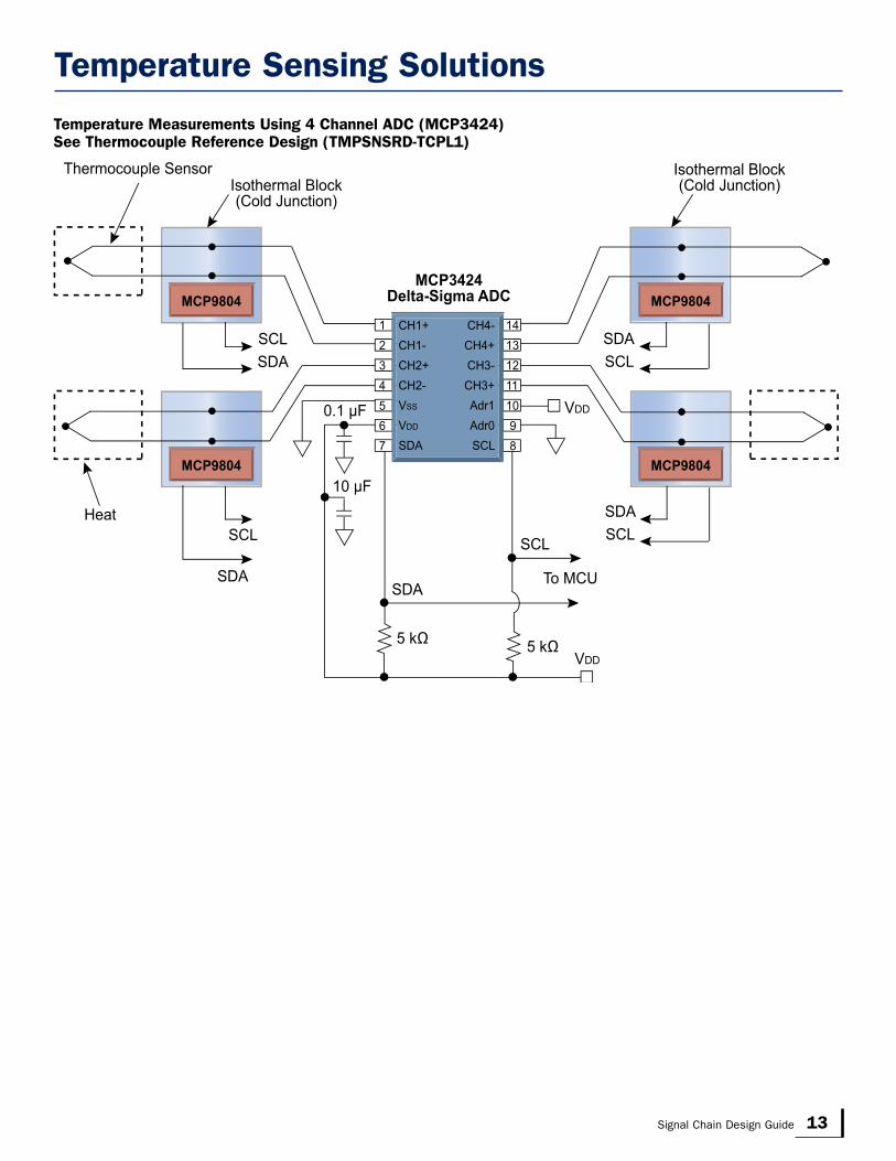
Temperature Measurements Using 4 Channel ADC (MCP3424) See Thermocouple Reference Design (TMPSNSRD-TCPL1)
12
1413
111098
MCP3424Delta-Sigma ADC
VDD
SCLSDA
Isothermal Block(Cold Junction)
Thermocouple Sensor
HeatSCL
0.1 µF
10 µF
SCL
SDA
VDD
5 kΩ
To MCU
SDASCL
SDASCL
3
12
4567
CH1+CH1-CH2+CH2-VSS
VDD
SDA
CH4-CH4+CH3-CH3+Adr1Adr0SCL
5 kΩ
SDA
Isothermal Block(Cold Junction)
MCP9804 MCP9804
MCP9804MCP9804
Temperature Sensing Solutions
14 Signal Chain Design Guide
The feedback capacitor (Cf) is used for circuit stability.
The device’s wiper resistance (Rw) is ignored for first order calculations. This is due to it being in series with the op amp input resistance and the op amp input impedance is very large.
Circuit Gain Equation
Programmable Gain AmplifierThe MCP6SX2 PGA Thermistor PICtail Demo Board features the MCP6S22 and MCP6S92 Programmable Gain Amplifiers (PGA). These devices overcome the non-linear response of a NTC thermistor, multiplex between two inputs and provide gain. It demonstrates the possibility of measuring multiple sensors and reducing the number of PIC microcontroller I/O pins used. Two on-board variable resistors allow users to experiment with different designs on the bench.
A complete solution is achieved by interfacing this board to the PICkit™ 1 Flash Starter Kit (see DS40051) and the Signal Analysis PICtail Daughter Board (see DS51476).
MCP6SX2 PGA Thermistor PICtail™ Demo Board (MCP6SX2DM-PICTLTH)
Vout = − Rbw × Vin Raw
rbw = rab × Wiper Code # of Resistors
Raw = # of Resistors − Wiper Code × Rab # of Resistors
PICkit™ 1 Serial AnalysisPC Program
PICkit 1 Flash Starter Kit
PC
USB
Hardware Software
PICkit 1 Firmware
PICA2Dlab.hexFirmware
14
14
Signal AnalysisPICtail Daughter Board
MCP6SX2 PGA ThermistorPICtail Demo Board
PGAMCP6S22
ThermistorTemperature
MCP6SX2 PGA ThermistorPICtail™ Demo Board
+5Test Point
GNDTest Point
CH0 InputTest Point
CH1 InputTest Point
Thermistor
VoltageDivider
Signal AnalysisPICtail Daughter Board
PICkit™ 1Flash Starter Kit
Serial EEPROM
PIC16F684
ADCPIC16F745
GND
+5
4
SPI BusVOUT
4
SPI™ Bus
GND
+5
to PCUSB
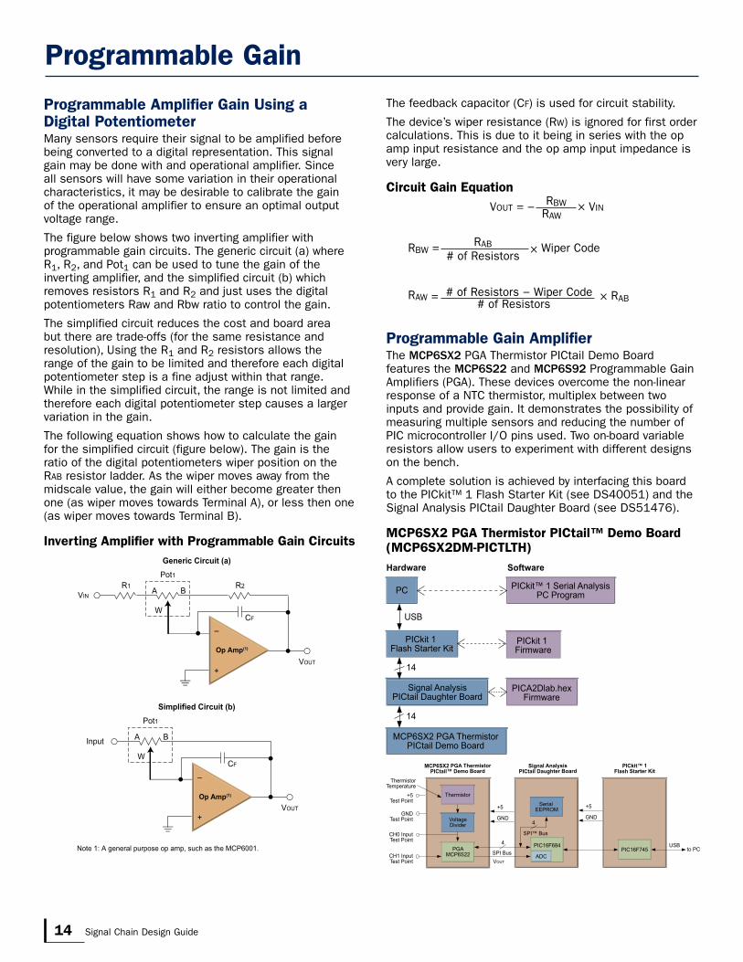
Programmable Gain
Programmable Amplifier Gain Using a Digital PotentiometerMany sensors require their signal to be amplified before being converted to a digital representation. This signal gain may be done with and operational amplifier. Since all sensors will have some variation in their operational characteristics, it may be desirable to calibrate the gain of the operational amplifier to ensure an optimal output voltage range.
The figure below shows two inverting amplifier with programmable gain circuits. The generic circuit (a) where R1, R2, and Pot1 can be used to tune the gain of the inverting amplifier, and the simplified circuit (b) which removes resistors R1 and R2 and just uses the digital potentiometers Raw and Rbw ratio to control the gain.
The simplified circuit reduces the cost and board area but there are trade-offs (for the same resistance and resolution), Using the R1 and R2 resistors allows the range of the gain to be limited and therefore each digital potentiometer step is a fine adjust within that range. While in the simplified circuit, the range is not limited and therefore each digital potentiometer step causes a larger variation in the gain.
The following equation shows how to calculate the gain for the simplified circuit (figure below). The gain is the ratio of the digital potentiometers wiper position on the Rab resistor ladder. As the wiper moves away from the midscale value, the gain will either become greater then one (as wiper moves towards Terminal A), or less then one (as wiper moves towards Terminal B).
Inverting Amplifier with Programmable Gain CircuitsGeneric Circuit (a)
Pot1
VOUT
VIN
R2R1
W
A B
Simplified Circuit (b)Pot1
VOUT
Input
CFW
A B
Note 1: A general purpose op amp, such as the MCP6001.
Op Amp(1)
+
–
CF
Op Amp(1)
+
–
15Signal Chain Design Guide
Sensor Calibration/Compensation
Sensor CharacteristicsSensor characteristics vary, both for device to device as well as for a given device over the operating conditions. To optimize system operation, this sensor variation may require some compensation. This compensation may simply address device to device variation, or be more dynamic to also address the variations of the device over the operating conditions. The system voltage and temperature may effect the sensor output characteristics such as output voltage offset and linearity. This conditioning circuit can also be used to optimize the range of the sensors conditioned signal into the Analog-to-Digital conversion circuit.
Depending on the sensor, the sensor’s output may either be voltage or a current. A possible compensation circuit for each output type will be discussed.
In this first case, the sensor generates an output voltage. Temperature sensors are typical sensors that generate a voltage output which varies unit to unit.
Voltage ControlA simple voltage control circuit (see figure below) can ensure that the sensors output voltage is optimized to the input range of the next stage in the signal chain. This circuit is a gain amplifier, where the R1 and R2 resistances determine the amplifier’s gain. The amplifier’s output voltage range is limited by the Vdd and Vss voltages. Controlling the Vos voltage can optimize the Vout voltage profile, based on the sensor’s output voltage (Vsen).
Inverting Amplifier (Voltage Gain)
Either a DAC or a Digital Potentiometer can be used to control the voltage at Vos. This device can be a non-volatile version so that at system power up the Vos voltage is at the calibrated voltage, programmed during manufacturing test, to address the sensor’s device to device variation. If dynamic control is desired, the DAC or Digital Potentiometer can be interfaced to a microcontroller so that dynamic changes to the Vos voltage compensate for the system conditions and non-linearity of the sensor.
Analog-to-DigitalConversion
Conditioning Circuit
(Optimizes Sensor’s Output)
Sensor
VOUT
R2
R1
VOS
VSEN VIN
VDD
Op Amp
+
–
VDD
Typically during the manufacturing stage the test system will write this compensation data into some non-volatile memory in the system which the microcontroller will use during normal operation to adjust the Vos voltage.
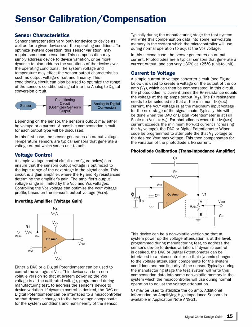
In this second case, the sensor generates an output current. Photodiodes are a typical sensors that generate a current output, and can vary ±30% at +25°C (unit-to-unit).
Current to VoltageA simple current to voltage converter circuit (see Figure below), is used to create a voltage on the output of the op amp (V1), which can then be compensated. In this circuit, the photodiodes Ipd current times the Rf resistance equals the voltage at the op amps output (V1). The Rf resistance needs to be selected so that at the minimum Ipd(max) current, the Vout voltage is at the maximum input voltage for the next stage of the signal chain. Typically this will be done when the DAC or Digital Potentiometer is at Full Scale (so Vout ≈ V1). For photodiodes where the Ipd(max) current exceeds the minimum Ipd(max) current (increasing the V1 voltage), the DAC or Digital Potentiometer Wiper code be programmed to attenuate the that V1 voltage to the desired Vout max voltage. This then compensates for the variation of the photodiode‘s Ipd current.
Photodiode Calibration (Trans-Impedance Amplifier)
This device can be a non-volatile version so that at system power up the voltage attenuation is at the level, programmed during manufacturing test, to address the sensor’s device to device variation. If dynamic control is desired, the DAC or Digital Potentiometer can be interfaced to a microcontroller so that dynamic changes to the voltage attenuation compensate for the system conditions and non-linearity of the sensor. Typically during the manufacturing stage the test system will write this compensation data into some non-volatile memory in the system which the microcontroller will use during normal operation to adjust the voltage attenuation.
Cf may be used to stabilize the op amp. Additional information on Amplifying High-Impedance Sensors is available in Application Note AN951.
RF
VPD
Op Amp
+
–
CF
RAB
V1
A
B CN
VOUTIPD
C(1)

16 Signal Chain Design Guide
Setting the DC Set Point for Sensor CircuitA common DAC application is digitally controlling the set point and/or calibration of parameters in a signal chain. The figure below shows controlling the DC set point of a light detector sensor using the MCP4728 12-bit quad DAC device. The DAC provides 4096 output steps. If G = 1 and internal reference voltage options are selected, then the internal 2.048 Vref would produce 500 µV of resolution.
If G = 2 is selected, the internal 2.048 Vref would produce 1 mV of resolution. If a smaller output step size is desired, the output range would need to be reduced. So, using gain of 1 is a better choice than using gain of 2 configuration option for smaller step size, but its full-scale range is one half of that of the gain of 2. Using a voltage divider at the DAC output is another method for obtaining a smaller step size.
Sensor Calibration/Compensation
Setting the DC Set Point
LDAC
8
10
9
7
6
VDD
3
1
2
4
5
VSS
VOUT A
VOUT D
VOUT C
VOUT B
VDD
SCL
SDA
RDY/BSY
R6
R3
R5
R4
0.1 µF
Analog Outputs
10 µF
To MCU
R1
R2
Comparator 1
Light VDD
VTRIP1
0.1 µF
R1
R2
Comparator 2
Light VDD
VTRIP2
0.1 µF
R1
R2
Comparator 3
Light VDD
VTRIP3
0.1 µF
R1
R2
Comparator 4
Light VDD
VTRIP4
0.1 µF
VOUT = VREF x Dn GX
VTRIP = VOUT x
R1 + R2
Where Dn = Input Code (0 to 4095) GX = Gain Selection (x1 or x2)
4096
R2
Quad DAC
RSENSE
MCP6544(1/4)
RSENSE
MCP6544(2/4)
RSENSE
MCP6544(3/4)
RSENSE
MCP6544(4/4)
–
+
MCP4728
–
+
–
+
–
+
17Signal Chain Design Guide
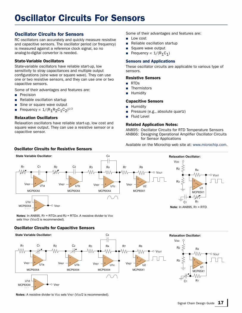
Oscillator Circuits for SensorsRC oscillators can accurately and quickly measure resistive and capacitive sensors. The oscillator period (or frequency) is measured against a reference clock signal, so no analog-to-digital convertor is needed.
State-Variable OscillatorsState-variable oscillators have reliable start-up, low sensitivity to stray capacitances and multiple output configurations (sine wave or square wave). They can use one or two resistive sensors, and they can use one or two capacitive sensors.
Some of their advantages and features are: Precision Reliable oscillation startup Sine or square wave output Frequency ∝ 1/(R1R2C1C2)1/2
Relaxation OscillatorsRelaxation oscillators have reliable start-up, low cost and square wave output. They can use a resistive sensor or a capacitive sensor.
Oscillator Circuits For Sensors
Oscillator Circuits for Resistive Sensors
Oscillator Circuits for Capacitive Sensors
VOUT
C2C1
VREF
–
+
–
+
–
+
–
+
C4
R4R1 R2
VREF VREF
R3 R7 R8
VREF
Notes: In AN895, R1 = RTDA and R2 = RTDA. A resistive divider to VDD
sets VREF (VDD/2 is recommended).
MCP6XX4 MCP6XX4 MCP6XX4
C1
VDD
–
+
R2
R3
MCP65X1
MCP65X1
U1a U1b U1c U2
State Variable Oscillator:
–
+. . .VREFMCP6XX4
Relaxation Oscillator:
U1
R1
R4
VOUT
Note: In AN895, R1 = RTD.
U1d
VOUT
C2C1
VREF
–
+
–
+
–
+
–
+
C4
R4R1 R2
VREF VREF
R3 R7 R8
VREF
Notes: A resistive divider to VDD sets VREF (VDD/2 is recommended).
MCP6XX4 MCP6XX4 MCP6XX4
C1
VDD
–
+
R2
R3
MCP65X1
MCP65X1
U1a U1b U1c U2
State Variable Oscillator:
–
+. . .VREFMCP6XX4
Relaxation Oscillator:
U1
R1
R4
VOUT
U1d
VOUT
C2C1
VREF
–
+
–
+
–
+
–
+
C4
R4R1 R2
VREF VREF
R3 R7 R8
VREF
Notes: A resistive divider to VDD sets VREF (VDD/2 is recommended).
MCP6XX4 MCP6XX4 MCP6XX4
C1
VDD
–
+
R2
R3
MCP65X1
MCP65X1
U1a U1b U1c U2
State Variable Oscillator:
–
+. . .VREFMCP6XX4
Relaxation Oscillator:
U1
R1
R4
VOUT
U1d
Some of their advantages and features are: Low cost Reliable oscillation startup Square wave output Frequency ∝ 1/(R1C1)
Sensors and ApplicationsThese oscillator circuits are applicable to various type of sensors.
Resistive Sensors RTDs Thermistors Humidity
Capacitive Sensors Humidity Pressure (e.g., absolute quartz) Fluid Level
Related Application Notes:AN895: Oscillator Circuits for RTD Temperature Sensors AN866: Designing Operational Amplifier Oscillator Circuits
for Sensor Applications
Available on the Microchip web site at: www.microchip.com.
18 Signal Chain Design Guide
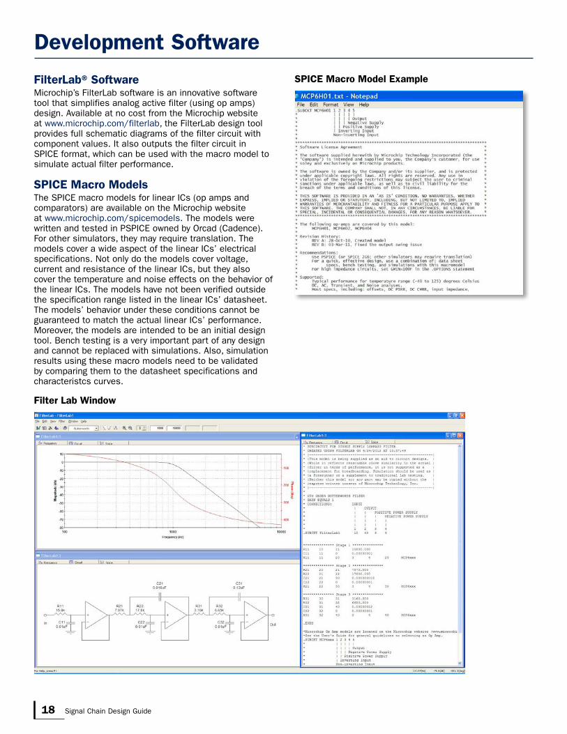
FilterLab® SoftwareMicrochip’s FilterLab software is an innovative software tool that simplifies analog active filter (using op amps) design. Available at no cost from the Microchip website at www.microchip.com/filterlab, the FilterLab design tool provides full schematic diagrams of the filter circuit with component values. It also outputs the filter circuit in SPICE format, which can be used with the macro model to simulate actual filter performance.
SPICE Macro ModelsThe SPICE macro models for linear ICs (op amps and comparators) are available on the Microchip website at www.microchip.com/spicemodels. The models were written and tested in PSPICE owned by Orcad (Cadence). For other simulators, they may require translation. The models cover a wide aspect of the linear ICs’ electrical specifications. Not only do the models cover voltage, current and resistance of the linear ICs, but they also cover the temperature and noise effects on the behavior of the linear ICs. The models have not been verified outside the specification range listed in the linear ICs’ datasheet. The models’ behavior under these conditions cannot be guaranteed to match the actual linear ICs’ performance. Moreover, the models are intended to be an initial design tool. Bench testing is a very important part of any design and cannot be replaced with simulations. Also, simulation results using these macro models need to be validated by comparing them to the datasheet specifications and characteristcs curves.
Filter Lab Window
SPICE Macro Model Example
Development Software
19Signal Chain Design Guide
Development ToolsThese following development boards support the development of signal chain applications. These product families may have other demonstration and evaluation boards that may also be useful. For more information visit www.microchip.com/analogtools.
Reference DesignsBattery
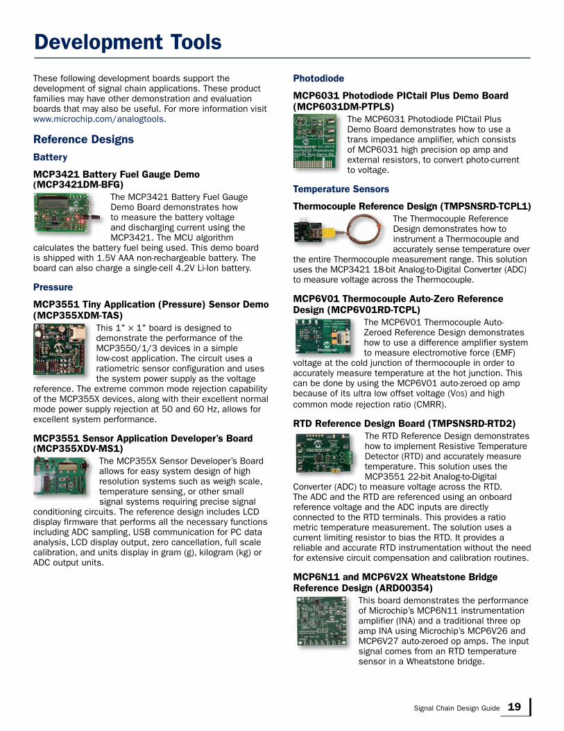
MCP3421 Battery Fuel Gauge Demo (MCP3421DM-BFG)
The MCP3421 Battery Fuel Gauge Demo Board demonstrates how to measure the battery voltage and discharging current using the MCP3421. The MCU algorithm
calculates the battery fuel being used. This demo board is shipped with 1.5V AAA non-rechargeable battery. The board can also charge a single-cell 4.2V Li-Ion battery.
Pressure
MCP3551 Tiny Application (Pressure) Sensor Demo (MCP355XDM-TAS)
This 1" × 1" board is designed to demonstrate the performance of the MCP3550/1/3 devices in a simple low-cost application. The circuit uses a ratiometric sensor configuration and uses the system power supply as the voltage
reference. The extreme common mode rejection capability of the MCP355X devices, along with their excellent normal mode power supply rejection at 50 and 60 Hz, allows for excellent system performance.
MCP3551 Sensor Application Developer’s Board (MCP355XDV-MS1)
The MCP355X Sensor Developer’s Board allows for easy system design of high resolution systems such as weigh scale, temperature sensing, or other small signal systems requiring precise signal
conditioning circuits. The reference design includes LCD display firmware that performs all the necessary functions including ADC sampling, USB communication for PC data analysis, LCD display output, zero cancellation, full scale calibration, and units display in gram (g), kilogram (kg) or ADC output units.
Photodiode
MCP6031 Photodiode PICtail Plus Demo Board (MCP6031DM-PTPLS)
The MCP6031 Photodiode PICtail Plus Demo Board demonstrates how to use a trans impedance amplifier, which consists of MCP6031 high precision op amp and external resistors, to convert photo-current to voltage.
Temperature Sensors
Thermocouple Reference Design (TMPSNSRD-TCPL1)The Thermocouple Reference Design demonstrates how to instrument a Thermocouple and accurately sense temperature over
the entire Thermocouple measurement range. This solution uses the MCP3421 18-bit Analog-to-Digital Converter (ADC) to measure voltage across the Thermocouple.
MCP6V01 Thermocouple Auto-Zero Reference Design (MCP6V01RD-TCPL)
The MCP6V01 Thermocouple Auto-Zeroed Reference Design demonstrates how to use a difference amplifier system to measure electromotive force (EMF)
voltage at the cold junction of thermocouple in order to accurately measure temperature at the hot junction. This can be done by using the MCP6V01 auto-zeroed op amp because of its ultra low offset voltage (Vos) and high common mode rejection ratio (CMRR).
RTD Reference Design Board (TMPSNSRD-RTD2)The RTD Reference Design demonstrates how to implement Resistive Temperature Detector (RTD) and accurately measure temperature. This solution uses the MCP3551 22-bit Analog-to-Digital
Converter (ADC) to measure voltage across the RTD. The ADC and the RTD are referenced using an onboard reference voltage and the ADC inputs are directly connected to the RTD terminals. This provides a ratio metric temperature measurement. The solution uses a current limiting resistor to bias the RTD. It provides a reliable and accurate RTD instrumentation without the need for extensive circuit com pensation and calibration routines.
MCP6N11 and MCP6V2X Wheatstone Bridge Reference Design (ARD00354)
This board demonstrates the performance of Microchip’s MCP6N11 instrumentation amplifier (INA) and a traditional three op amp INA using Microchip’s MCP6V26 and MCP6V27 auto-zeroed op amps. The input signal comes from an RTD temperature sensor in a Wheatstone bridge.
20 Signal Chain Design Guide
Development ToolsDemonstration BoardsADCs
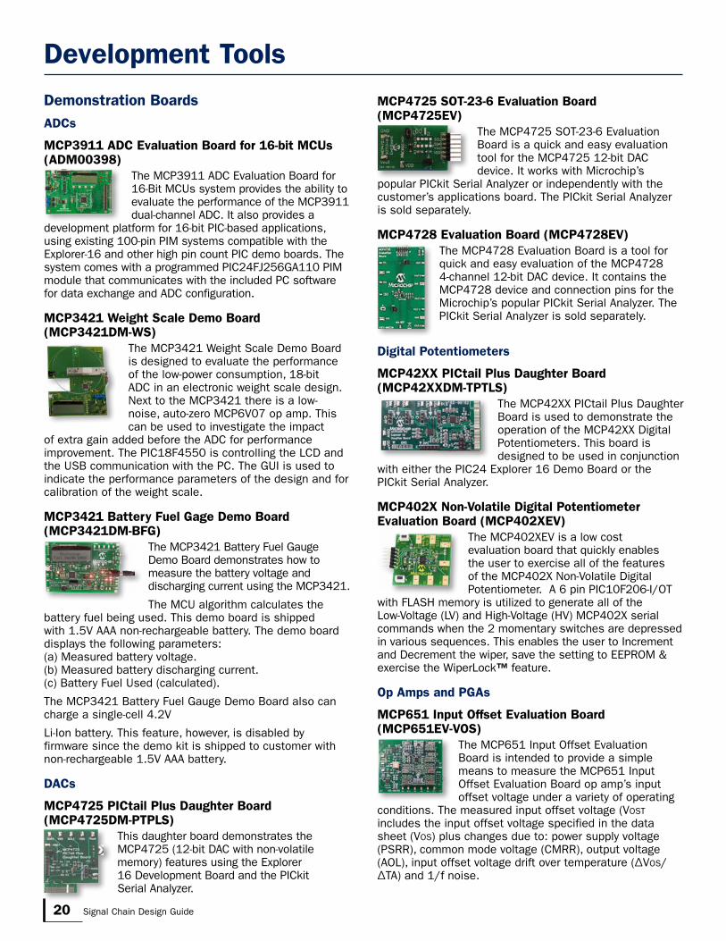
MCP3911 ADC Evaluation Board for 16-bit MCUs (ADM00398)
The MCP3911 ADC Evaluation Board for 16-Bit MCUs system provides the ability to evaluate the performance of the MCP3911 dual-channel ADC. It also provides a
development platform for 16-bit PIC-based applications, using existing 100-pin PIM systems compatible with the Explorer-16 and other high pin count PIC demo boards. The system comes with a programmed PIC24FJ256GA110 PIM module that communicates with the included PC software for data exchange and ADC configuration.
MCP3421 Weight Scale Demo Board (MCP3421DM-WS)
The MCP3421 Weight Scale Demo Board is designed to evaluate the performance of the low-power consumption, 18-bit ADC in an electronic weight scale design. Next to the MCP3421 there is a low-noise, auto-zero MCP6V07 op amp. This can be used to investigate the impact
of extra gain added before the ADC for performance improvement. The PIC18F4550 is controlling the LCD and the USB communication with the PC. The GUI is used to indicate the performance parameters of the design and for calibration of the weight scale.
MCP3421 Battery Fuel Gage Demo Board (MCP3421DM-BFG)
The MCP3421 Battery Fuel Gauge Demo Board demonstrates how to measure the battery voltage and discharging current using the MCP3421.
The MCU algorithm calculates the battery fuel being used. This demo board is shipped with 1.5V AAA non-rechargeable battery. The demo board displays the following parameters: (a) Measured battery voltage. (b) Measured battery discharging current. (c) Battery Fuel Used (calculated).
The MCP3421 Battery Fuel Gauge Demo Board also can charge a single-cell 4.2V
Li-Ion battery. This feature, however, is disabled by firmware since the demo kit is shipped to customer with non-rechargeable 1.5V AAA battery.
DACs
MCP4725 PICtail Plus Daughter Board (MCP4725DM-PTPLS)
This daughter board demonstrates the MCP4725 (12-bit DAC with non-volatile memory) features using the Explorer 16 Development Board and the PICkit Serial Analyzer.
MCP4725 SOT-23-6 Evaluation Board (MCP4725EV)
The MCP4725 SOT-23-6 Evaluation Board is a quick and easy evaluation tool for the MCP4725 12-bit DAC device. It works with Microchip’s
popular PICkit Serial Analyzer or independently with the customer’s applications board. The PICkit Serial Analyzer is sold separately.
MCP4728 Evaluation Board (MCP4728EV)The MCP4728 Evaluation Board is a tool for quick and easy evaluation of the MCP4728 4-channel 12-bit DAC device. It contains the MCP4728 device and connection pins for the Microchip’s popular PICkit Serial Analyzer. The PICkit Serial Analyzer is sold separately.
Digital Potentiometers
MCP42XX PICtail Plus Daughter Board (MCP42XXDM-TPTLS)
The MCP42XX PICtail Plus Daughter Board is used to demonstrate the operation of the MCP42XX Digital Potentiometers. This board is designed to be used in conjunction
with either the PIC24 Explorer 16 Demo Board or the PICkit Serial Analyzer.
MCP402X Non-Volatile Digital Potentiometer Evaluation Board (MCP402XEV)
The MCP402XEV is a low cost evaluation board that quickly enables the user to exercise all of the features of the MCP402X Non-Volatile Digital Potentiometer. A 6 pin PIC10F206-I/OT
with FLASH memory is utilized to generate all of the Low-Voltage (LV) and High-Voltage (HV) MCP402X serial commands when the 2 momentary switches are depressed in various sequences. This enables the user to Increment and Decrement the wiper, save the setting to EEPROM & exercise the WiperLock™ feature.
Op Amps and PGAs
MCP651 Input Offset Evaluation Board (MCP651EV-VOS)
The MCP651 Input Offset Evaluation Board is intended to provide a simple means to measure the MCP651 Input Offset Evaluation Board op amp’s input offset voltage under a variety of operating
conditions. The measured input offset voltage (Vost includes the input offset voltage specified in the data sheet (Vos) plus changes due to: power supply voltage (PSRR), common mode voltage (CMRR), output voltage (AOL), input offset voltage drift over temperature (ΔVos/ΔTA) and 1/f noise.
21Signal Chain Design Guide
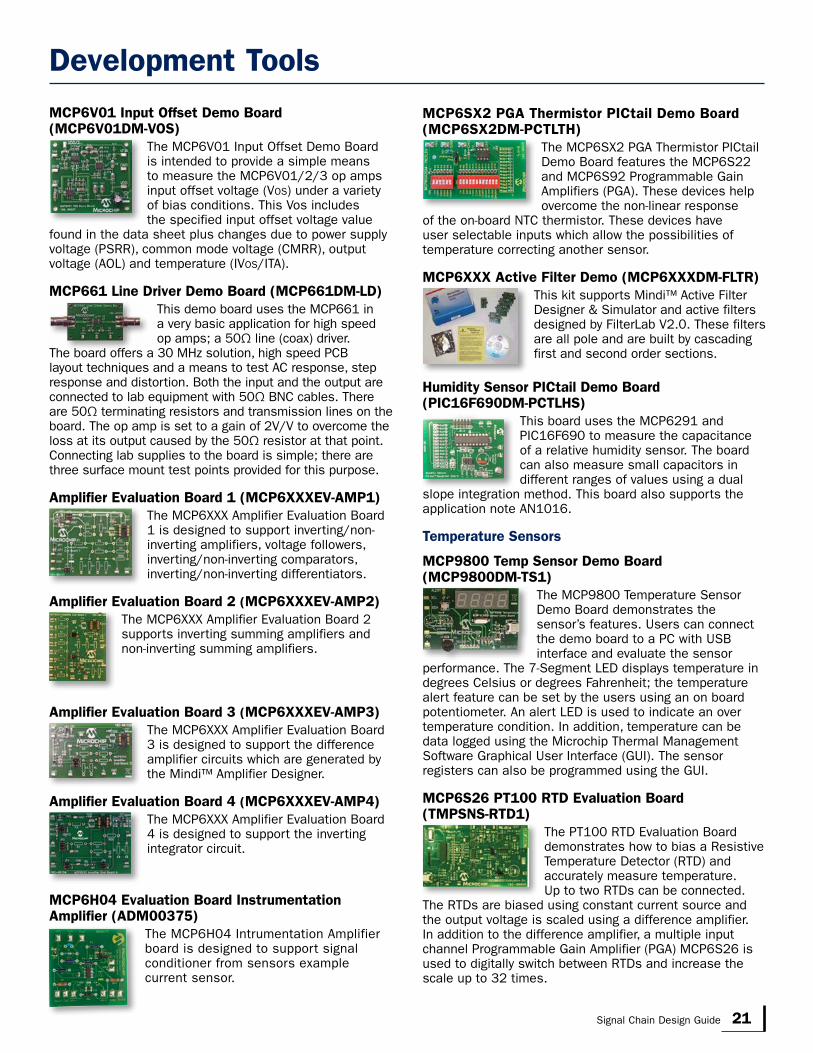
Development ToolsMCP6V01 Input Offset Demo Board (MCP6V01DM-VOS)
The MCP6V01 Input Offset Demo Board is intended to provide a simple means to measure the MCP6V01/2/3 op amps input offset voltage (Vos) under a variety of bias conditions. This Vos includes the specified input offset voltage value
found in the data sheet plus changes due to power supply voltage (PSRR), common mode voltage (CMRR), output voltage (AOL) and temperature (IVos/ITA).
MCP661 Line Driver Demo Board (MCP661DM-LD)This demo board uses the MCP661 in a very basic application for high speed op amps; a 50Ω line (coax) driver.
The board offers a 30 MHz solution, high speed PCB layout techniques and a means to test AC response, step response and distortion. Both the input and the output are connected to lab equipment with 50Ω BNC cables. There are 50Ω terminating resistors and transmission lines on the board. The op amp is set to a gain of 2V/V to overcome the loss at its output caused by the 50Ω resistor at that point. Connecting lab supplies to the board is simple; there are three surface mount test points provided for this purpose.
Amplifier Evaluation Board 1 (MCP6XXXEV-AMP1)The MCP6XXX Amplifier Evaluation Board 1 is designed to support inverting/non-inverting amplifiers, voltage followers, inverting/non-inverting comparators, inverting/non-inverting differentiators.
Amplifier Evaluation Board 2 (MCP6XXXEV-AMP2)The MCP6XXX Amplifier Evaluation Board 2 supports inverting summing amplifiers and non-inverting summing amplifiers.
Amplifier Evaluation Board 3 (MCP6XXXEV-AMP3)The MCP6XXX Amplifier Evaluation Board 3 is designed to support the difference amplifier circuits which are generated by the Mindi™ Amplifier Designer.
Amplifier Evaluation Board 4 (MCP6XXXEV-AMP4)The MCP6XXX Amplifier Evaluation Board 4 is designed to support the inverting integrator circuit.
MCP6H04 Evaluation Board Instrumentation Amplifier (ADM00375)
The MCP6H04 Intrumentation Amplifier board is designed to support signal conditioner from sensors example current sensor.
MCP6SX2 PGA Thermistor PICtail Demo Board (MCP6SX2DM-PCTLTH)
The MCP6SX2 PGA Thermistor PICtail Demo Board features the MCP6S22 and MCP6S92 Programmable Gain Amplifiers (PGA). These devices help overcome the non-linear response
of the on-board NTC thermistor. These devices have user selectable inputs which allow the possibilities of temperature correcting another sensor.
MCP6XXX Active Filter Demo (MCP6XXXDM-FLTR)This kit supports Mindi™ Active Filter Designer & Simulator and active filters designed by FilterLab V2.0. These filters are all pole and are built by cascading first and second order sections.
Humidity Sensor PICtail Demo Board (PIC16F690DM-PCTLHS)
This board uses the MCP6291 and PIC16F690 to measure the capacitance of a relative humidity sensor. The board can also measure small capacitors in different ranges of values using a dual
slope integration method. This board also supports the application note AN1016.
Temperature Sensors
MCP9800 Temp Sensor Demo Board (MCP9800DM-TS1)
The MCP9800 Temperature Sensor Demo Board demonstrates the sensor’s features. Users can connect the demo board to a PC with USB interface and evaluate the sensor
performance. The 7-Segment LED displays temperature in degrees Celsius or degrees Fahrenheit; the temperature alert feature can be set by the users using an on board potentiometer. An alert LED is used to indicate an over temperature condition. In addition, temperature can be data logged using the Microchip Thermal Management Software Graphical User Interface (GUI). The sensor registers can also be programmed using the GUI.
MCP6S26 PT100 RTD Evaluation Board (TMPSNS-RTD1)
The PT100 RTD Evaluation Board demonstrates how to bias a Resistive Temperature Detector (RTD) and accurately measure temperature. Up to two RTDs can be connected.
The RTDs are biased using constant current source and the output voltage is scaled using a difference amplifier. In addition to the difference amplifier, a multiple input channel Programmable Gain Amplifier (PGA) MCP6S26 is used to digitally switch between RTDs and increase the scale up to 32 times.

22 Signal Chain Design Guide
Related Support MaterialThe following literature is available on the Microchip web site: www.microchip.com/appnotes. There are additional application notes that may be useful.
Application Related DocumentationSensor Conditioning Circuits Overview
AN866: Designing Operational Amplifier Oscillator Circuits For Sensor ApplicationsOperational amplifier (op amp) oscillators can be used to accurately measure resistive and capacitive sensors. Oscillator design can be simplified by using the procedure discussed in this application note. The derivation of the design equations provides a method to select the passive components and determine the influence of each component on the frequency of oscillation. The procedure will be demonstrated by analyzing two state-variable RC op-amp oscillator circuits.
AN990: Analog Sensor Conditioning Circuits, An OverviewAnalog sensors produce a change in an electrical property to indicate a change in its environment. This change in electrical property needs to be conditioned by an analog circuit before conversion to digital. Further processing occurs in the digital domain but is not addressed in this application note.
Delta-Sigma ADCs
AN1156: Battery Fuel Measurement Using Delta-Sigma ADC DevicesThis application note reviews the battery fuel measurement using the MCU and ADC devices. Developing battery fuel measurement in this manner provides flexible solutions and enables economic management.
DS21841: Analog-to-Digital Converter Design Guide
SAR ADCs
AN246: Driving the Analog Inputs of a SAR A/D ConverterThis application note delves into the issues surrounding the SAR converter’s input and conversion nuances to insure that the converter is handled properly from the beginning of the design phase.
AN688: Layout Tips for 12-Bit A/D Converter ApplicationThis application note provides basic 12-bit layout guidelines, ending with a review of issues to be aware of. Examples of good layout and bad layout implementations are presented throughout.
AN693: Understanding A/D Converter Performance SpecificationsThis application note describes the specifications used to quantify the performance of A/D converters and give the reader a better understanding of the significance of those specifications in an application.
AN842: Differential ADC Biasing Techniques, Tips and TricksTrue differential converters can offer many advantages over single-ended input A/D Converters (ADC). In addition to their common mode rejection ability, these converters can also be used to overcome many DC biasing limitations of common signal conditioning circuits.
Utility Metering
DS01008: Utility Metering Solutions
Digital Potentiometers
AN691: Optimizing the Digital Potentiometer in Precision CircuitsIn this application note, circuit ideas are presented that use the necessary design techniques to mitigate errors, consequently optimizing the performance of the digital potentiometer.
AN692: Using a Digital Potentiometer to Optimize a Precision Single Supply Photo DetectThis application note shows how the adjustability of the digital potentiometer can be used to an advantage in photosensing circuits.
AN1080: Understanding Digital Potentiometer Resistance VariationsThis application note discusses how process, voltage and temperature effect the resistor network’s characteristics, specifications and techniques to improve system performance.
AN1316A: Using Digital Potentiometers for Programmable Amplifier GainThis application note discusses implementations of programmable gain circuits using an op amp and a digital potentiometer. This discussion includes implementation details for the digital potentiometer’s resistor network.

23Signal Chain Design Guide
Op Amps
AN1302: Current Sensing Circuit Concepts and FundamentalsThis application note provides an overview of current sensing circuit concepts and fundamentals. It introduces current sensing techniques and focuses on three typical high-side current sensing implementations, with their specific advantages and disadvantages.
AN679: Temperature Sensing TechnologiesCovers the most popular temperature sensor technologies and helps determine the most appropriate sensor for an application.
AN681: Reading and Using Fast Fourier Transformation (FFT)Discusses the use of frequency analysis (FFTs), time analysis and DC analysis techniques. It emphasizes Analog-to-Digital converter applications.
AN684: Single Supply Temperature Sensing with ThermocouplesFocuses on thermocouple circuit solutions. It builds from signal conditioning components to complete application circuits.
AN695: Interfacing Pressure Sensors to Microchip’s Analog PeripheralsShows how to condition a Wheatstone bridge sensor using simple circuits. A piezoresistive pressure sensor application is used to illustrate the theory.
AN699: Anti-Aliasing, Analog Filters for Data Acquisition SystemsA tutorial on active analog filters and their most common applications.
AN722: Operational Amplifier Topologies and DC SpecificationsDefines op amp DC specifications found in a data sheet. It shows where these specifications are critical in application circuits.
AN723: Operational Amplifier AC Specifications and ApplicationsDefines op amp AC specifications found in a data sheet. It shows where these specifications are critical in application circuits.
AN866: Designing Operational Amplifier Oscillator Circuits For Sensor ApplicationsGives simple design procedures for op amp oscillators. These circuits are used to accurately measure resistive and capacitive sensors.
AN884: Driving Capacitive Loads With Op AmpsExplains why all op amps tend to have problems driving large capacitive loads. A simple, one resistor compensation scheme is given that gives much better performance.
AN951: Amplifying High-Impedance Sensors, Photodiode ExampleShows how to condition the current out of a high-impedance sensor. A photodiode detector illustrates the theory.
AN990: Analog Sensor Conditioning Circuits, An OverviewGives an overview of the many sensor types, applications and conditioning circuits.
AN1014: Measuring Small Changes in Capacitive SensorsThis application note shows a switched capacitor circuit that uses a PIC microcontroller, and minimal external passive components, to measure small changes in capacitance. The values are very repeatable under constant environmental conditions.
AN1177: Op Amp Precision Design: DC ErrorsThis application note covers the essential background information and design theory needed to design a precision DC circuit using op amps.
AN1228: Op Amp Precision Design: Random NoiseThis application note covers the essential background information and design theory needed to design low noise, precision op amp circuits. The focus is on simple, results oriented methods and approximations useful for circuits with a low-pass response.
AN1258: Op Amp Precision Design: PCB Layout TechniquesThis application note covers Printed Circuit Board (PCB) effects encountered in high (DC) precision op amp circuits. It provides techniques for improving the performance, giving more flexibility in solving a given design problem. It demonstrates one important factor necessary to convert a good schematic into a working precision design.
Related Support Material

24 Signal Chain Design Guide
Related Support MaterialAN1297: Microchip’s Op Amp SPICE Macro ModelsThis application note covers the function and use of Microchip’s op amp SPICE macro models. It does not explain how to use the circuit simulator but will give the user a better understanding how the model behaves and tips on convergence issues.
AN1353: Rectifiers, Op Amp Peak Detectors and ClampsThis application note covers a wide range of application, such as half-wave rectifiers, full-wave rectifiers, peak detectors and clamps.
Temperature Sensing
AN929: Temperature Measurement Circuits for Embedded ApplicationsThis application note shows how to select a temperature sensor and conditioning circuit to maximize the measurement accuracy and simplify the interface to the microcontroller.
AN1001: IC Temperature Sensor Accuracy Compensation with a PIC MicrocontrollerThis application note derives an equation that describes the sensor’s typical non-linear characteristics, which can be used to compensate for the sensor’s accuracy error over the specified operating temperature range.
AN1154: Precision RTD Instrumentation for Temperature SensingPrecision RTD (Resistive Temperature Detector) instrumentation is key for high performance thermal management applications. This application note shows how to use a high resolution Delta-Sigma Analog-to-Digital converter, and two resistors to measure RTD resistance ratiometrically. A ±0.1°C accuracy and ±0.01°C measurement resolution can be achieved across the RTD temperature range of −200°C to +800°C with a single point calibration.
Product Related DocumentationSensor Conditioning Circuits Overview
AN895: Oscillator Circuits for RTD Temperature SensorsThis application note shows how to design a temperature sensor oscillator circuit using Microchip’s low-cost MCP6001 operational amplifier (op amp) and the MCP6541 comparator. Oscillator circuits can be used to provide an accurate temperature measurement with a Resistive Temperature Detector (RTD) sensor. Oscillators provide a frequency output that is proportional to temperature and are easily integrated into a microcontroller system.
Delta-Sigma ADCs
AN1007: Designing with the MCP3551 Delta-Sigma ADCThe MCP3551 delta-sigma ADC is a high-resolution converter. This application note discusses various design techniques to follow when using this device. Typical application circuits are discussed first, followed by a section on noise analysis.
AN1030: Weigh Scale Applications for the MCP3551This application note focusses specifically on load cells, a type of strain gauge that is typically used for measuring weight. Even more specifically, the focus is on fully active, temperature compensated load cells whose change in differential output voltage with a rated load is 2 mV to 4 mV per volt of excitation (the excitation voltage being the difference between the +Input and the −Input terminals of the load cell).
SAR ADCs
AN845: Communicating With The MCP3221 Using PIC MicrocontrollersThis application note will cover communications between the MCP3221 12-bit A/D Converter and a PIC microcontroller. The code supplied with this application note is written as relocatable assembly code.
25Signal Chain Design Guide
Passive Keyless Entry (PKE)
TB090: MCP2030 Three-Channel Analog Front-End Device OverviewThis tech brief summarizes the technical features of the MCP2030 and describes how the three channel stand-alone analog front-end device can be used for various bidirectional communication applications.
AN1024: PKE System Design Using the PIC16F639This application note described how to make hands-free reliable passive keyless entry applications using the PIC16F639, a dual die solution device that includes both MCP2030 and PIC16F636.
Op Amps
AN1016: Detecting Small Capacitive Sensors Using the MCP6291 and PIC16F690 DevicesThe circuit discussed here uses an op amp and a microcontroller to implement a dual slope integrator and timer. It gives accurate results, and is appropriate for small capacitive sensors, such as capacitive humidity sensors.
Programmable Gain Amplifier (PGA)
AN248: Interfacing MCP6S2X PGAs to PIC MicrocontrollersThis application note shows how to program the six channel MCP6S26 PGA gains, channels and shutdown registers using the PIC16C505 microcontroller.
AN865: Sensing Light with a Programmable Gain AmplifierThis application notes discusses how Microchip’s Programmable Gain Amplifiers (PGAs) can be effectively used in position photo sensing applications minus the headaches of amplifier stability.
AN897: Thermistor Temperature Sensing with MCP6SX2 PGAsShows how to use a Programmable Gain Amplifier (PGA) to linearize the response of a thermistor, and to achieve a wider temperature measurement range.
Temperature Sensing
AN981: Interfacing a MCP9700 Analog Temperature Sensor to a PIC MicrocontrollerAnalog output silicon temperature sensors offer an easy-to-use alternative to traditional temperature sensors, such as thermistors. The MCP9700 offers many system-level advantages, including the integration of the temperature sensor and signal-conditioning circuitry on a single chip. Analog output sensors are especially suited for embedded systems due to their linear output. This application note will discuss system integration, firmware implementation and PCB layout techniques for using the MCP9700 in an embedded system.
AN988: Interfacing a MCP9800 I2C Digital Temperature Sensor to a PIC MicrocontrollerThis application note will discuss system integration, firmware implementation and PCB layout techniques for using the MCP9800 in an embedded system.
AN1306: Thermocouple Circuit Using MCP6V01 and PIC18F2550This application note shows how to use a difference amplifier system to measure electromotive force (EMF) voltage at the cold junction of thermocouple in order to accurately measure temperature at the hot junction. This can be done by using the MCP6V01 auto-zeroed op amp because of its extremely low input offset volt age (Vos) and very high common mode rejection ratio (CMRR). The microcontroller PIC18F2550 used in this circuit has internal comparator voltage reference (CVref). This solution minimizes cost by using resources internal to the PIC18F2550 to achieve rea sonable resolution without an external ADC.
Related Support Material

26
Signal C
hain Design G
uide
linearLinear: Op amps
Device# per
Package
GBWP (kHz) Typ.
iq (µa/amp.)
Typ.
Vos (±µV) Max.
Supply Voltage (V)
Temperature range (°C)
rail- to-rail
i/OFeatures Packages Featured Demo Board Op amp Category
MCP6441/2/4 1, 2, 4 9 0.45 4,500 1.8 to 6.0 −40 to +125 I/O Low Quiescent Current SOIC, MSOP, 2 × 3 TDFN, TSSOP, SOT-23, SC-70 SOIC8EV, SOIC14EV –
MCP6031/2/3/4 1, 2, 1, 4 10 1 150 1.8 to 5.5 −40 to +125 I/O Low Power Mode on MCP6033 SOIC, MSOP, TSSOP, DFN, SOT-23
MCP6031DM-PCTL, SOIC8EV, SOIC14EV
Low Offset, Low Power
MCP6041/2/3/4 1, 2, 1, 4 14 1 3,000 1.4 to 6.0 −40 to +85, −40 to +125 I/O Low Power Mode on MCP6043 PDIP, SOIC, MSOP, TSSOP,
SOT-23 SOIC8EV, SOIC14EV General Purpose, Low Power
MCP6141/2/3/4 1, 2, 1, 4 100 1 3,000 1.4 to 6.0 −40 to +85, −40 to +125 I/O GMIN = 10, Low Power Mode
on MCP6143PDIP, SOIC, MSOP, TSSOP, SOT-23 SOIC8EV, SOIC14EV General Purpose,
Low Power
MCP606/7/8/9 1, 2, 1, 4 155 25 250 2.5 to 6.0 −40 to +85 O Low Power Mode on MCP608 PDIP, SOIC, TSSOP, DFN, SOT-23 SOIC8EV, SOIC14EV Low Offset
MCP616/7/8/9 1, 2, 1, 4 190 25 150 2.3 to 5.5 −40 to +85 O Low Power Mode on MCP618 PDIP, SOIC, TSSOP SOIC8EV, SOIC14EV Low Offset
MCP6231/1R/1U/2/4 1, 1, 1, 2, 4 300 30 5,000 1.8 to 6.0 −40 to +125 I/O – PDIP, SOIC, MSOP, TSSOP,
DFN, SOT-23, SC-70VSUPEV2, SOIC8EV, SOIC14EV General Purpose
MCP6051/2/4 1, 2, 4 385 45 150 1.8 to 6.0 −40 to +125 I/O – SOIC, TSSOP, TDFN SOIC8EV, SOIC14EV Low Offset
MCP6241/1R/1U/2/4 1, 1, 1, 2, 4 550 70 5,000 1.8 to 5.5 −40 to +125 I/O – PDIP, SOIC, MSOP, TSSOP,
DFN, SOT-23, SC-70VSUPEV2, SOIC8EV, SOIC14EV General Purpose
MCP6061/2/4 1, 2, 4 730 90 150 1.8 to 6.0 −40 to +125 I/O – SOIC, TSSOP, TDFN SOIC8EV, SOIC14EV Low Offset
MCP6001/1R/1U/2/4 1, 1, 1, 2, 4 1,000 170 4,500 1.8 to 6.0 −40 to +85,
−40 to +125 I/O – PDIP, SOIC, MSOP, TSSOP, SOT-23, SC-70
MCP6SX2DM-PICTLPD, SOIC8EV, SOIC14EV
General Purpose
MCP6401/2/4 1, 2, 4 1,000 45 4,500 1.8 to 6.0 −40 to +125/150 I/O Low Quiescent Current SOIC, MSOP, 2 × 3 TDFN,
TSSOP, SOT-23, SC-70 SOIC8EV, SOIC14EV –
MCP6L01/2/4 1, 2, 4 1,000 85 5,000 1.8 to 6.0 −40 to +125 I/O – PDIP, SOIC, MSOP, TSSOP, SOT-23, SC-70 – –
MCP6071/2/4 1, 2, 4 1,200 170 150 1.8 to 6.0 −40 to +125 I/O – SOIC, TSSOP, TDFN SOIC8EV, SOIC14EV Low Offset
MCP6H01/2/4 1, 2, 4 1,200 135 3,500 3.5 to 16 −40 to +125 O High Voltage SOIC, 2 × 3 TDFN, TSSOP, SOT-23, SC-70 – –
MCP6H81/2/4 1, 2, 4 5,500 700 1,000 3.5 to 12V −40 to +125 O High Voltage SOIC, TDFN, TSSOP – –
MCP6H91/2/4 1, 2, 4 10,000 2,000 1,000 3.5 to 12V −40 to +125 O High Voltage SOIC, TDFN, TSSOP – –
MCP6271/1R/2/3/4/5 1, 1, 2, 1, 4, 2 2,000 240 3,000 2.0 to 6.0 −40 to +125 I/O
Low Power Mode on MCP6273, Cascaded Gain with MCP6275
PDIP, SOIC, MSOP, TSSOP, SOT-23
MCP6XXXDM-FLTR, SOIC8EV, SOIC14EV General Purpose
MCP6L71/2/3/4 1, 2, 1, 4 2,000 150 4,000 2.0 to 6.0 −40 to +125 I/O Low Power Mode on MCP6L73 PDIP, SOIC, MSOP, TSSOP, SOT-23
MCP6XXXDM-FLTR, SOIC8EV, SOIC14EV –
MCP601/1R/2/3/4 1, 1, 2, 1, 4 2,800 325 2,000 2.7 to 6.0 −40 to +85,
−40 to +125 O Low Power Mode on MCP603 PDIP, SOIC, TSSOP, SOT-23 SOIC8EV, SOIC14EV General Purpose
MCP6L1/2/4 1, 2, 4 2,800 200 3,000 2.7 to 6.0 −40 to +125 O – PDIP, SOIC, TSSOP, SOT-23 SOIC8EV, SOIC14EV –
MCP6286 1 3,500 720 1,500 2.2 to 5.5 −40 to +125 O Low Noise SOT-23 VSUPEV2 Low Noise
MCP6281/1R/2/3/4/5 1, 1, 2, 1, 4, 2 5,000 570 3,000 2.2 to 6.0 −40 to +125 I/O
Low Power Mode on MCP6283, Cascaded Gain with MCP6285
PDIP, SOIC, MSOP, TSSOP, SOT-23
VSUPEV2, SOIC8EV, SOIC14EV General Purpose
MCP6021/1R/2/3/4 1, 1, 2, 1, 4 10,000 1,350 500, 250 2.5 to 5.5 −40 to +85,
−40 to +125 I/O Low Power Mode on MCP6023 PDIP, SOIC, MSOP, TSSOP, SOT-23
MCP6XXXEV-AMP1, SOIC8EV, SOIC14EV Low Offset
MCP6291/1R/2/3/4/5 1, 1, 2, 1, 4, 2 10,000 1,300 3,000 2.4 to 6.0 −40 to +125 I/O
Low Power Mode on MCP6293, Cascaded Gain with MCP6295
PDIP, SOIC, MSOP, TSSOP, SOT-23
PIC16F690DM-PCTLHS, SOIC8EV, SOIC14EV
General Purpose
MCP6L91/2/4 1, 2, 4 10,000 850 4,000 2.4 to 6.0 −40 to +125 I/O – PDIP, SOIC, MSOP, TSSOP, SOT-23
PIC16F690DM-PCTLHS, SOIC8EV, SOIC14EV
–
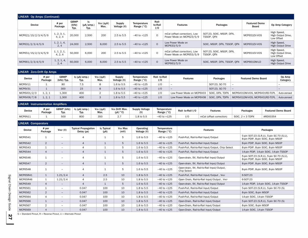
27
Signal C
hain Design G
uide
Linear: Op amps (Continued)
Device# per
Package
GBWP (kHz) Typ.
iq (µa/amp.)
Typ.
Vos (±µV) Max.
Supply Voltage (V)
Temperature range (°C)
rail- to-rail
i/OFeatures Packages
Featured Demo Board
Op amp Category
MCP621/1S/2/3/4/5/9 1, 2, 3, 1, 4, 2, 4 20,000 2,500 200 2.5 to 5.5 −40 to +125 O mCal (offset correction), Low
Power Mode on MCP623/5/9SOT-23, SOIC, MSOP, DFN, TSSOP, QFN MCP651EV-VOS
High Speed, High Output Drive, Low Offset
MCP631/2/3/4/5/9 1, 2, 1, 4, 2, 4 24,000 2,500 8,000 2.5 to 5.5 −40 to +125 O Low Power Mode on
MCP633/5/9 SOIC, MSOP, DFN, TSSOP, QFN MCP651EV-VOS High Speed, High Output Drive
MCP651/1S/2/3/4/5/9 1, 1, 2, 1, 4, 2, 4 50,000 6,000 200 2.5 to 5.5 −40 to +125 O mCal (offset correction), Low
Power Mode on MCP653/5/9SOT-23, SOIC, MSOP, DFN, TSSOP, QFN MCP651EV-VOS
High Speed, High Output Drive, Low Offset
MCP661/2/3/4/5/9 1, 2, 1, 4, 2, 4 60,000 6,000 8,000 2.5 to 5.5 −40 to +125 O Low Power Mode on
MCP663/5/9 SOIC, MSOP, DFN, TSSOP, QFN MCP661DM-LD High Speed, High Output Drive
Linear: Zero-Drift Op amps
Device# per
PackageGBWP
(kHz) Typ.iq (µa/amp.)
Typ.Vos (±µV)
Max.Supply
Voltage (V)Temperature range (°C)
rail- to-rail i/O
Features Packages Featured Demo BoardOp amp Category
MCP6V11 1 80 7.5 8 1.6 to 5.5 −40 to +125 I/O – SOT-23, SC-70 – –
MCP6V31 1 300 23 8 1.6 to 5.5 −40 to +125 I/O – SOT-23, SC-70 – –
MCP6V01/2/3 1, 2, 1 1,300 400 2 1.8 to 5.5 −40 to +125 I/O Low Power Mode on MCP6V03 SOIC, DFN, TDFN MCP6V01DM-VOS, MCP6V01RD-TCPL Auto-zeroed
MCP6V06/7/8 1, 2, 1 1,300 400 3 1.8 to 5.5 −40 to +125 I/O Low Power Mode on MCP6V08 SOIC, DFN, TDFN MCP6V01DM-VOS, MCP6V01RD-TCPL Auto-zeroed
Linear: instrumentation amplifiers
Device# per
PackageGBWP (kHz)
Typ.iq (µa/amp.)
Typ.Vos (±µV)
Max.Vos Drift Max.
(µV/°C) Supply Voltage
(V)Temperature range (°C)
rail- to-rail i/O Features Packages Featured Demo Board
MCP6N11 1 500 800 350 2.7 1.8 to 5.5 −40 to +125 I/O mCal (offset correction) SOIC, 2 × 3 TDFN ARD00354
Linear: Comparators
Device# per
PackageVref (V)
Typical Propagation Delay (μs)
iq Typical (μa)
Vos Max (mV)
Operating Voltage (V)
Temperature range (°C)
Features Packages
MCP6541 1 – 4 1 5 1.6 to 5.5 −40 to +125 Push-Pull, Rail-to-Rail Input/Output 5-pin SOT-23 (S,R,U), 5-pin SC-70 (S,U), 8-pin PDIP, 8-pin SOIC, 8-pin MSOP
MCP6542 2 – 4 1 5 1.6 to 5.5 −40 to +125 Push-Pull, Rail-to-Rail Input/Output 8-pin PDIP, 8-pin SOIC, 8-pin MSOP
MCP6543 1 – 4 1 5 1.6 to 5.5 −40 to +125 Push-Pull, Rail-to-Rail Input/Output, Chip Select 8-pin PDIP, 8-pin SOIC, 8-pin MSOP
MCP6544 4 – 4 1 5 1.6 to 5.5 −40 to +125 Push-Pull, Rail-to-Rail Input/Output 14-pin PDIP, 14-pin SOIC, 14-pin TSSOP
MCP6546 1 – 4 1 5 1.6 to 5.5 −40 to +125 Open-drain, 9V, Rail-to-Rail Input/Output 5-pin SOT-23 (S,R,U), 5-pin SC-70 (S,U), 8-pin PDIP, 8-pin SOIC, 8-pin MSOP
MCP6547 2 – 4 1 5 1.6 to 5.5 −40 to +125 Open-drain, 9V, Rail-to-Rail Input/Output 8-pin PDIP, 8-pin SOIC, 8-pin MSOP
MCP6548 1 – 4 1 5 1.6 to 5.5 −40 to +125 Open-drain, 9V, Rail-to-Rail Input/Output, Chip Select 8-pin PDIP, 8-pin SOIC, 8-pin MSOP
MCP65R41 1 1.21/2.4 4 2.5 10 1.8 to 5.5 −40 to +125 Push-Pull, Rail-to-Rail Input/Output , Vref 6-SOT-23
MCP65R46 1 1.21/2.4 4 2.5 10 1.8 to 5.5 −40 to +125 Open Drain, Rail-to-Rail Input/Output , Vref 6-SOT-23
MCP6549 4 – 4 1 5 1.6 to 5.5 −40 to +125 Open-drain, 9V, Rail-to-Rail Input/Output 14-pin PDIP, 14-pin SOIC, 14-pin TSSOP
MCP6561 1 – 0.047 100 10 1.8 to 5.5 −40 to +125 Push-Pull, Rail-to-Rail Input/Output 5-pin SOT-23 (S,R,U), 5-pin SC-70 (S)
MCP6562 2 – 0.047 100 10 1.8 to 5.5 −40 to +125 Push-Pull, Rail-to-Rail Input/Output 8-pin SOIC, 8-pin MSOP
MCP6564 4 – 0.047 100 10 1.8 to 5.5 −40 to +125 Push-Pull, Rail-to-Rail Input/Output 14-pin SOIC, 14-pin TSSOP
MCP6566 1 – 0.047 100 10 1.8 to 5.5 −40 to +125 Open-Drain, Rail-to-Rail Input/Output 5-pin SOT-23 (S,R,U), 5-pin SC-70 (S)
MCP6567 2 – 0.047 100 10 1.8 to 5.5 −40 to +125 Open-Drain, Rail-to-Rail Input/Output 8-pin SOIC, 8-pin MSOP
MCP6569 4 – 0.047 100 10 1.8 to 5.5 −40 to +125 Open-Drain, Rail-to-Rail Input/Output 14-pin SOIC, 14-pin TSSOP
S = Standard Pinout, R = Reverse Pinout, U = Alternate Pinout
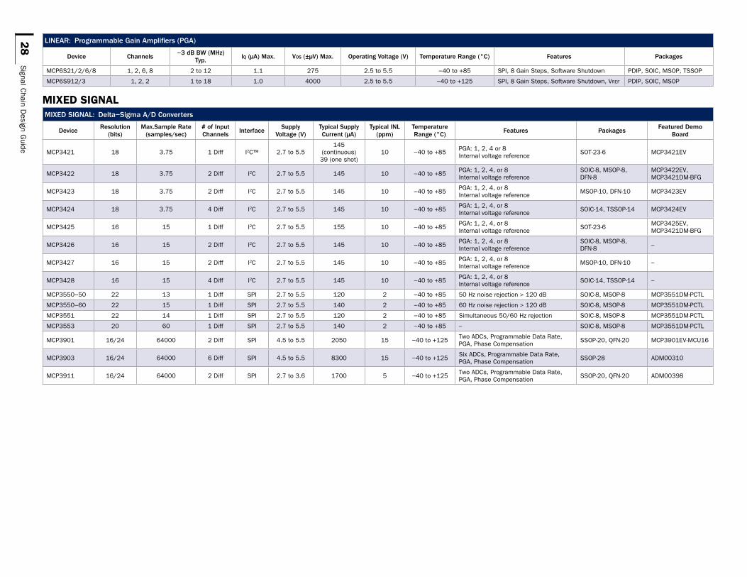
28
Signal C
hain Design G
uide
Linear: Programmable Gain amplifiers (PGa)
Device Channels−3 dB BW (MHz)
Typ.iq (µa) Max. Vos (±µV) Max. Operating Voltage (V) Temperature range (°C) Features Packages
MCP6S21/2/6/8 1, 2, 6, 8 2 to 12 1.1 275 2.5 to 5.5 −40 to +85 SPI, 8 Gain Steps, Software Shutdown PDIP, SOIC, MSOP, TSSOP
MCP6S912/3 1, 2, 2 1 to 18 1.0 4000 2.5 to 5.5 −40 to +125 SPI, 8 Gain Steps, Software Shutdown, Vref PDIP, SOIC, MSOP
Mixed SignalMixeD SiGnaL: Delta−Sigma a/D Converters
Deviceresolution
(bits)Max.Sample rate
(samples/sec)# of input Channels
interfaceSupply
Voltage (V)Typical Supply Current (µa)
Typical inL (ppm)
Temperature range (°C)
Features PackagesFeatured Demo
Board
MCP3421 18 3.75 1 Diff I2C™ 2.7 to 5.5145
(continuous) 39 (one shot)
10 −40 to +85 PGA: 1, 2, 4 or 8 Internal voltage reference SOT-23-6 MCP3421EV
MCP3422 18 3.75 2 Diff I2C 2.7 to 5.5 145 10 −40 to +85 PGA: 1, 2, 4, or 8 Internal voltage reference
SOIC-8, MSOP-8, DFN-8
MCP3422EV, MCP3421DM-BFG
MCP3423 18 3.75 2 Diff I2C 2.7 to 5.5 145 10 −40 to +85 PGA: 1, 2, 4, or 8 Internal voltage reference MSOP-10, DFN-10 MCP3423EV
MCP3424 18 3.75 4 Diff I2C 2.7 to 5.5 145 10 −40 to +85 PGA: 1, 2, 4, or 8 Internal voltage reference SOIC-14, TSSOP-14 MCP3424EV
MCP3425 16 15 1 Diff I2C 2.7 to 5.5 155 10 −40 to +85 PGA: 1, 2, 4, or 8 Internal voltage reference SOT-23-6 MCP3425EV,
MCP3421DM-BFG
MCP3426 16 15 2 Diff I2C 2.7 to 5.5 145 10 −40 to +85 PGA: 1, 2, 4, or 8 Internal voltage reference
SOIC-8, MSOP-8, DFN-8 –
MCP3427 16 15 2 Diff I2C 2.7 to 5.5 145 10 −40 to +85 PGA: 1, 2, 4, or 8 Internal voltage reference MSOP-10, DFN-10 –
MCP3428 16 15 4 Diff I2C 2.7 to 5.5 145 10 −40 to +85 PGA: 1, 2, 4, or 8 Internal voltage reference SOIC-14, TSSOP-14 –
MCP3550−50 22 13 1 Diff SPI 2.7 to 5.5 120 2 −40 to +85 50 Hz noise rejection > 120 dB SOIC-8, MSOP-8 MCP3551DM-PCTL
MCP3550−60 22 15 1 Diff SPI 2.7 to 5.5 140 2 −40 to +85 60 Hz noise rejection > 120 dB SOIC-8, MSOP-8 MCP3551DM-PCTL
MCP3551 22 14 1 Diff SPI 2.7 to 5.5 120 2 −40 to +85 Simultaneous 50/60 Hz rejection SOIC-8, MSOP-8 MCP3551DM-PCTL
MCP3553 20 60 1 Diff SPI 2.7 to 5.5 140 2 −40 to +85 – SOIC-8, MSOP-8 MCP3551DM-PCTL
MCP3901 16/24 64000 2 Diff SPI 4.5 to 5.5 2050 15 −40 to +125 Two ADCs, Programmable Data Rate, PGA, Phase Compensation SSOP-20, QFN-20 MCP3901EV-MCU16
MCP3903 16/24 64000 6 Diff SPI 4.5 to 5.5 8300 15 −40 to +125 Six ADCs, Programmable Data Rate, PGA, Phase Compensation SSOP-28 ADM00310
MCP3911 16/24 64000 2 Diff SPI 2.7 to 3.6 1700 5 −40 to +125 Two ADCs, Programmable Data Rate, PGA, Phase Compensation SSOP-20, QFN-20 ADM00398
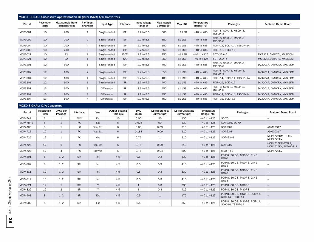
29
Signal C
hain Design G
uide
MixeD SiGnaL: Successive approximation register (Sar) a/D Converters
Part #resolution
(bits)Max.Sample rate
(samples/sec)# of input Channels
input Type interfaceinput Voltage
range (V)Max. Supply Current (µa)
Max. inL Temperature range (°C)
Packages Featured Demo Board
MCP3001 10 200 1 Single−ended SPI 2.7 to 5.5 500 ±1 LSB −40 to +85 PDIP−8, SOIC−8, MSOP−8, TSSOP−8 –
MCP3002 10 200 2 Single−ended SPI 2.7 to 5.5 650 ±1 LSB −40 to +85 PDIP−8, SOIC−8, MSOP−8, TSSOP−8 –
MCP3004 10 200 4 Single−ended SPI 2.7 to 5.5 550 ±1 LSB −40 to +85 PDIP−14, SOIC−14, TSSOP−14 –
MCP3008 10 200 8 Single−ended SPI 2.7 to 5.5 550 ±1 LSB −40 to +85 PDIP−16, SOIC−16 –
MCP3021 10 22 1 Single−ended I2C™ 2.7 to 5.5 250 ±1 LSB −40 to +125 SOT−23A−5 MCP3221DM-PCTL, MXSIGDM
MCP3221 12 22 1 Single−ended I2C 2.7 to 5.5 250 ±2 LSB −40 to +125 SOT−23A−5 MCP3221DM-PCTL, MXSIGDM
MCP3201 12 100 1 Single−ended SPI 2.7 to 5.5 400 ±1 LSB −40 to +85 PDIP−8, SOIC−8, MSOP−8, TSSOP−8 DV3201A, DVMCPA, MXSIGDM
MCP3202 12 100 2 Single−ended SPI 2.7 to 5.5 550 ±1 LSB −40 to +85 PDIP−8, SOIC−8, MSOP−8, TSSOP−8 DV3201A, DVMCPA, MXSIGDM
MCP3204 12 100 4 Single−ended SPI 2.7 to 5.5 400 ±1 LSB −40 to +85 PDIP−14, SOIC−14, TSSOP−14 DV3204A, DVMCPA, MXSIGDM
MCP3208 12 100 8 Single−ended SPI 2.7 to 5.5 400 ±1 LSB −40 to +85 PDIP−16, SOIC−16 DV3204A, DVMCPA, MXSIGDM
MCP3301 13 100 1 Differential SPI 2.7 to 5.5 450 ±1 LSB −40 to +85 PDIP−8, SOIC−8, MSOP−8, TSSOP−8 DV3201A, DVMCPA, MXSIGDM
MCP3302 13 100 2 Differential SPI 2.7 to 5.5 450 ±1 LSB −40 to +85 PDIP−14, SOIC−14, TSSOP−14 DV3204A, DVMCPA, MXSIGDM
MCP3304 13 100 4 Differential SPI 2.7 to 5.5 450 ±1 LSB −40 to +85 PDIP−16, SOIC−16 DV3204A, DVMCPA, MXSIGDM
MixeD SiGnaL: D/a Converters
Part #resolution
(Bits)DaCs per Package
interface VrefOutput Settling
Time (µs)DnL (LSB)
Typical Standby Current (µa)
Typical Operating Current (µa)
Temperature range (°C)
Packages Featured Demo Board
MCP47A1 6 1 I2C™ Ext 15 0.05 90 130 −40 to +125 SC-70 –
MCP47DA1 6 1 I2C Ext 6 0.025 90 130 −40 to +125 SOT-23-6, SC-70 –
MCP4706 8 1 I2C Vdd, ext 6 0.05 0.09 210 −40 to +125 SOT-23-6 ADM00317
MCP4716 10 1 I2C Vdd, Ext 6 0.188 0.09 210 −40 to +125 SOT-23-6 ADM00317
MCP4725 12 1 I2C Vdd 6 0.75 1 210 −40 to +125 SOT−23−6 MCP4725DM-PTPLS, MCP4725EV
MCP4726 12 1 I2C Vdd, Ext 6 0.75 0.09 210 −40 to +125 SOT-23-6 MCP4725DM-PTPLS, MCP4725EV, ADM00317
MCP4728 12 4 I2C Int/Vdd 6 0.75 0.04 800 −40 to +125 MSOP−10 MCP4728EV
MCP4801 8 1, 2 SPI Int 4.5 0.5 0.3 330 −40 to +125 PDIP-8, SOIC-8, MSOP-8, 2 × 3 DFN-8 –
MCP4802 8 1, 2 SPI Int 4.5 0.5 0.3 415 −40 to +125 PDIP-8, SOIC-8, MSOP-8, 2 × 3 DFN-8 –
MCP4811 10 1, 2 SPI Int 4.5 0.5 0.3 330 −40 to +125 PDIP-8, SOIC-8, MSOP-8, 2 × 3 DFN-8 –
MCP4812 10 1, 2 SPI Int 4.5 0.5 0.3 415 −40 to +125 PDIP-8, SOIC-8, MSOP-8, 2 × 3 DFN-8 –
MCP4821 12 1 SPI Y 4.5 1 0.3 330 −40 to +125 PDIP-8, SOIC-8, MSOP-8 –
MCP4822 12 2 SPI Y 4.5 1 0.3 415 −40 to +125 PDIP-8, SOIC-8, MSOP-8 –
MCP4901 8 1, 2 SPI Ext 4.5 0.5 1 175 −40 to +125 PDIP-8, SOIC-8, MSOP-8, PDIP-14, SOIC-14, TSSOP-14 –
MCP4902 8 1, 2 SPI Ext 4.5 0.5 1 350 −40 to +125 PDIP-8, SOIC-8, MSOP-8, PDIP-14, SOIC-14, TSSOP-14 –
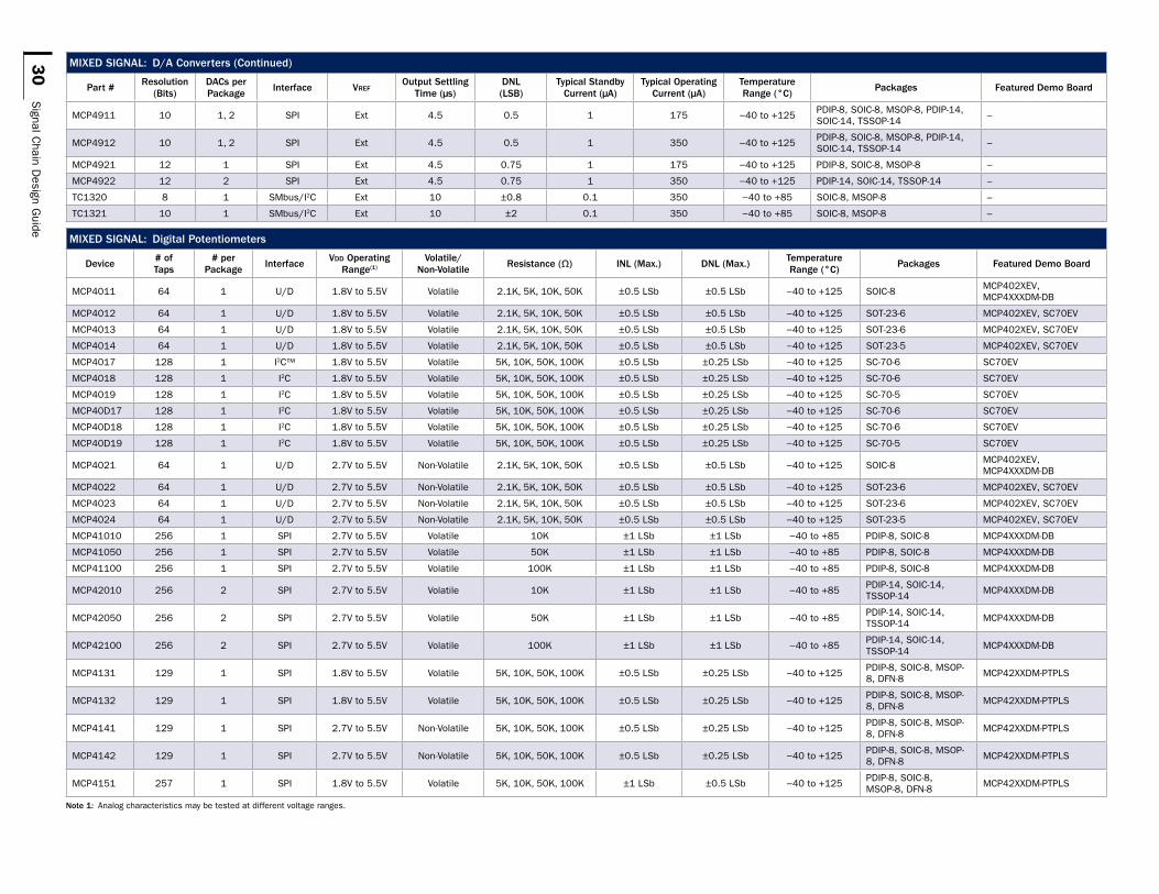
30
Signal C
hain Design G
uide
MixeD SiGnaL: D/a Converters (Continued)
Part #resolution
(Bits)DaCs per Package
interface VrefOutput Settling
Time (µs)DnL (LSB)
Typical Standby Current (µa)
Typical Operating Current (µa)
Temperature range (°C)
Packages Featured Demo Board
MCP4911 10 1, 2 SPI Ext 4.5 0.5 1 175 −40 to +125 PDIP-8, SOIC-8, MSOP-8, PDIP-14, SOIC-14, TSSOP-14 –
MCP4912 10 1, 2 SPI Ext 4.5 0.5 1 350 −40 to +125 PDIP-8, SOIC-8, MSOP-8, PDIP-14, SOIC-14, TSSOP-14 –
MCP4921 12 1 SPI Ext 4.5 0.75 1 175 −40 to +125 PDIP-8, SOIC-8, MSOP-8 –
MCP4922 12 2 SPI Ext 4.5 0.75 1 350 −40 to +125 PDIP-14, SOIC-14, TSSOP-14 –
TC1320 8 1 SMbus/I2C Ext 10 ±0.8 0.1 350 −40 to +85 SOIC-8, MSOP-8 –
TC1321 10 1 SMbus/I2C Ext 10 ±2 0.1 350 −40 to +85 SOIC-8, MSOP-8 –
MixeD SiGnaL: Digital Potentiometers
Device# of Taps
# per Package
interfaceVdd Operating
range(1)Volatile/
non-Volatileresistance (Ω) inL (Max.) DnL (Max.)
Temperature range (°C)
Packages Featured Demo Board
MCP4011 64 1 U/D 1.8V to 5.5V Volatile 2.1K, 5K, 10K, 50K ±0.5 LSb ±0.5 LSb −40 to +125 SOIC-8 MCP402XEV, MCP4XXXDM-DB
MCP4012 64 1 U/D 1.8V to 5.5V Volatile 2.1K, 5K, 10K, 50K ±0.5 LSb ±0.5 LSb −40 to +125 SOT-23-6 MCP402XEV, SC70EV
MCP4013 64 1 U/D 1.8V to 5.5V Volatile 2.1K, 5K, 10K, 50K ±0.5 LSb ±0.5 LSb −40 to +125 SOT-23-6 MCP402XEV, SC70EV
MCP4014 64 1 U/D 1.8V to 5.5V Volatile 2.1K, 5K, 10K, 50K ±0.5 LSb ±0.5 LSb −40 to +125 SOT-23-5 MCP402XEV, SC70EV
MCP4017 128 1 I2C™ 1.8V to 5.5V Volatile 5K, 10K, 50K, 100K ±0.5 LSb ±0.25 LSb −40 to +125 SC-70-6 SC70EV
MCP4018 128 1 I2C 1.8V to 5.5V Volatile 5K, 10K, 50K, 100K ±0.5 LSb ±0.25 LSb −40 to +125 SC-70-6 SC70EV
MCP4019 128 1 I2C 1.8V to 5.5V Volatile 5K, 10K, 50K, 100K ±0.5 LSb ±0.25 LSb −40 to +125 SC-70-5 SC70EV
MCP40D17 128 1 I2C 1.8V to 5.5V Volatile 5K, 10K, 50K, 100K ±0.5 LSb ±0.25 LSb −40 to +125 SC-70-6 SC70EV
MCP40D18 128 1 I2C 1.8V to 5.5V Volatile 5K, 10K, 50K, 100K ±0.5 LSb ±0.25 LSb −40 to +125 SC-70-6 SC70EV
MCP40D19 128 1 I2C 1.8V to 5.5V Volatile 5K, 10K, 50K, 100K ±0.5 LSb ±0.25 LSb −40 to +125 SC-70-5 SC70EV
MCP4021 64 1 U/D 2.7V to 5.5V Non-Volatile 2.1K, 5K, 10K, 50K ±0.5 LSb ±0.5 LSb −40 to +125 SOIC-8 MCP402XEV, MCP4XXXDM-DB
MCP4022 64 1 U/D 2.7V to 5.5V Non-Volatile 2.1K, 5K, 10K, 50K ±0.5 LSb ±0.5 LSb −40 to +125 SOT-23-6 MCP402XEV, SC70EV
MCP4023 64 1 U/D 2.7V to 5.5V Non-Volatile 2.1K, 5K, 10K, 50K ±0.5 LSb ±0.5 LSb −40 to +125 SOT-23-6 MCP402XEV, SC70EV
MCP4024 64 1 U/D 2.7V to 5.5V Non-Volatile 2.1K, 5K, 10K, 50K ±0.5 LSb ±0.5 LSb −40 to +125 SOT-23-5 MCP402XEV, SC70EV
MCP41010 256 1 SPI 2.7V to 5.5V Volatile 10K ±1 LSb ±1 LSb −40 to +85 PDIP-8, SOIC-8 MCP4XXXDM-DB
MCP41050 256 1 SPI 2.7V to 5.5V Volatile 50K ±1 LSb ±1 LSb −40 to +85 PDIP-8, SOIC-8 MCP4XXXDM-DB
MCP41100 256 1 SPI 2.7V to 5.5V Volatile 100K ±1 LSb ±1 LSb −40 to +85 PDIP-8, SOIC-8 MCP4XXXDM-DB
MCP42010 256 2 SPI 2.7V to 5.5V Volatile 10K ±1 LSb ±1 LSb −40 to +85 PDIP-14, SOIC-14, TSSOP-14 MCP4XXXDM-DB
MCP42050 256 2 SPI 2.7V to 5.5V Volatile 50K ±1 LSb ±1 LSb −40 to +85 PDIP-14, SOIC-14, TSSOP-14 MCP4XXXDM-DB
MCP42100 256 2 SPI 2.7V to 5.5V Volatile 100K ±1 LSb ±1 LSb −40 to +85 PDIP-14, SOIC-14, TSSOP-14 MCP4XXXDM-DB
MCP4131 129 1 SPI 1.8V to 5.5V Volatile 5K, 10K, 50K, 100K ±0.5 LSb ±0.25 LSb −40 to +125 PDIP-8, SOIC-8, MSOP-8, DFN-8 MCP42XXDM-PTPLS
MCP4132 129 1 SPI 1.8V to 5.5V Volatile 5K, 10K, 50K, 100K ±0.5 LSb ±0.25 LSb −40 to +125 PDIP-8, SOIC-8, MSOP-8, DFN-8 MCP42XXDM-PTPLS
MCP4141 129 1 SPI 2.7V to 5.5V Non-Volatile 5K, 10K, 50K, 100K ±0.5 LSb ±0.25 LSb −40 to +125 PDIP-8, SOIC-8, MSOP-8, DFN-8 MCP42XXDM-PTPLS
MCP4142 129 1 SPI 2.7V to 5.5V Non-Volatile 5K, 10K, 50K, 100K ±0.5 LSb ±0.25 LSb −40 to +125 PDIP-8, SOIC-8, MSOP-8, DFN-8 MCP42XXDM-PTPLS
MCP4151 257 1 SPI 1.8V to 5.5V Volatile 5K, 10K, 50K, 100K ±1 LSb ±0.5 LSb −40 to +125 PDIP-8, SOIC-8, MSOP-8, DFN-8 MCP42XXDM-PTPLS
note 1: Analog characteristics may be tested at different voltage ranges.
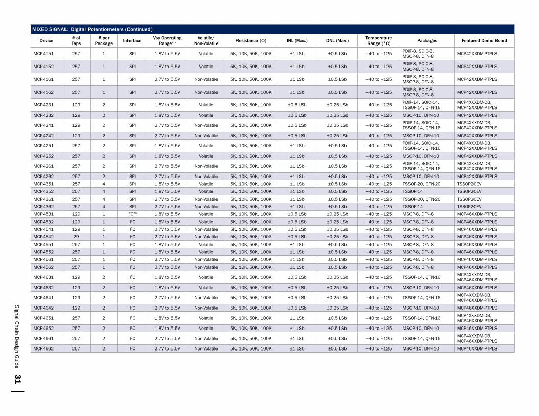
31
Signal C
hain Design G
uide
MixeD SiGnaL: Digital Potentiometers (Continued)
Device# of Taps
# per Package
interfaceVdd Operating
range(1)Volatile/
non-Volatileresistance (Ω) inL (Max.) DnL (Max.)
Temperature range (°C)
Packages Featured Demo Board
MCP4151 257 1 SPI 1.8V to 5.5V Volatile 5K, 10K, 50K, 100K ±1 LSb ±0.5 LSb −40 to +125 PDIP-8, SOIC-8, MSOP-8, DFN-8 MCP42XXDM-PTPLS
MCP4152 257 1 SPI 1.8V to 5.5V Volatile 5K, 10K, 50K, 100K ±1 LSb ±0.5 LSb −40 to +125 PDIP-8, SOIC-8, MSOP-8, DFN-8 MCP42XXDM-PTPLS
MCP4161 257 1 SPI 2.7V to 5.5V Non-Volatile 5K, 10K, 50K, 100K ±1 LSb ±0.5 LSb −40 to +125 PDIP-8, SOIC-8, MSOP-8, DFN-8 MCP42XXDM-PTPLS
MCP4162 257 1 SPI 2.7V to 5.5V Non-Volatile 5K, 10K, 50K, 100K ±1 LSb ±0.5 LSb −40 to +125 PDIP-8, SOIC-8, MSOP-8, DFN-8 MCP42XXDM-PTPLS
MCP4231 129 2 SPI 1.8V to 5.5V Volatile 5K, 10K, 50K, 100K ±0.5 LSb ±0.25 LSb −40 to +125 PDIP-14, SOIC-14, TSSOP-14, QFN-16
MCP4XXXDM-DB, MCP42XXDM-PTPLS
MCP4232 129 2 SPI 1.8V to 5.5V Volatile 5K, 10K, 50K, 100K ±0.5 LSb ±0.25 LSb −40 to +125 MSOP-10, DFN-10 MCP42XXDM-PTPLS
MCP4241 129 2 SPI 2.7V to 5.5V Non-Volatile 5K, 10K, 50K, 100K ±0.5 LSb ±0.25 LSb −40 to +125 PDIP-14, SOIC-14, TSSOP-14, QFN-16
MCP4XXXDM-DB, MCP42XXDM-PTPLS
MCP4242 129 2 SPI 2.7V to 5.5V Non-Volatile 5K, 10K, 50K, 100K ±0.5 LSb ±0.25 LSb −40 to +125 MSOP-10, DFN-10 MCP42XXDM-PTPLS
MCP4251 257 2 SPI 1.8V to 5.5V Volatile 5K, 10K, 50K, 100K ±1 LSb ±0.5 LSb −40 to +125 PDIP-14, SOIC-14, TSSOP-14, QFN-16
MCP4XXXDM-DB, MCP42XXDM-PTPLS
MCP4252 257 2 SPI 1.8V to 5.5V Volatile 5K, 10K, 50K, 100K ±1 LSb ±0.5 LSb −40 to +125 MSOP-10, DFN-10 MCP42XXDM-PTPLS
MCP4261 257 2 SPI 2.7V to 5.5V Non-Volatile 5K, 10K, 50K, 100K ±1 LSb ±0.5 LSb −40 to +125 PDIP-14, SOIC-14, TSSOP-14, QFN-16
MCP4XXXDM-DB, MCP42XXDM-PTPLS
MCP4262 257 2 SPI 2.7V to 5.5V Non-Volatile 5K, 10K, 50K, 100K ±1 LSb ±0.5 LSb −40 to +125 MSOP-10, DFN-10 MCP42XXDM-PTPLS
MCP4351 257 4 SPI 1.8V to 5.5V Volatile 5K, 10K, 50K, 100K ±1 LSb ±0.5 LSb −40 to +125 TSSOP-20, QFN-20 TSSOP20EV
MCP4352 257 4 SPI 1.8V to 5.5V Volatile 5K, 10K, 50K, 100K ±1 LSb ±0.5 LSb −40 to +125 TSSOP-14 TSSOP20EV
MCP4361 257 4 SPI 2.7V to 5.5V Non-Volatile 5K, 10K, 50K, 100K ±1 LSb ±0.5 LSb −40 to +125 TSSOP-20, QFN-20 TSSOP20EV
MCP4362 257 4 SPI 2.7V to 5.5V Non-Volatile 5K, 10K, 50K, 100K ±1 LSb ±0.5 LSb −40 to +125 TSSOP-14 TSSOP20EV
MCP4531 129 1 I2C™ 1.8V to 5.5V Volatile 5K, 10K, 50K, 100K ±0.5 LSb ±0.25 LSb −40 to +125 MSOP-8, DFN-8 MCP46XXDM-PTPLS
MCP4532 129 1 I2C 1.8V to 5.5V Volatile 5K, 10K, 50K, 100K ±0.5 LSb ±0.25 LSb −40 to +125 MSOP-8, DFN-8 MCP46XXDM-PTPLS
MCP4541 129 1 I2C 2.7V to 5.5V Non-Volatile 5K, 10K, 50K, 100K ±0.5 LSb ±0.25 LSb −40 to +125 MSOP-8, DFN-8 MCP46XXDM-PTPLS
MCP4542 29 1 I2C 2.7V to 5.5V Non-Volatile 5K, 10K, 50K, 100K ±0.5 LSb ±0.25 LSb −40 to +125 MSOP-8, DFN-8 MCP46XXDM-PTPLS
MCP4551 257 1 I2C 1.8V to 5.5V Volatile 5K, 10K, 50K, 100K ±1 LSb ±0.5 LSb −40 to +125 MSOP-8, DFN-8 MCP46XXDM-PTPLS
MCP4552 257 1 I2C 1.8V to 5.5V Volatile 5K, 10K, 50K, 100K ±1 LSb ±0.5 LSb −40 to +125 MSOP-8, DFN-8 MCP46XXDM-PTPLS
MCP4561 257 1 I2C 2.7V to 5.5V Non-Volatile 5K, 10K, 50K, 100K ±1 LSb ±0.5 LSb −40 to +125 MSOP-8, DFN-8 MCP46XXDM-PTPLS
MCP4562 257 1 I2C 2.7V to 5.5V Non-Volatile 5K, 10K, 50K, 100K ±1 LSb ±0.5 LSb −40 to +125 MSOP-8, DFN-8 MCP46XXDM-PTPLS
MCP4631 129 2 I2C 1.8V to 5.5V Volatile 5K, 10K, 50K, 100K ±0.5 LSb ±0.25 LSb −40 to +125 TSSOP-14, QFN-16 MCP4XXXDM-DB, MCP46XXDM-PTPLS
MCP4632 129 2 I2C 1.8V to 5.5V Volatile 5K, 10K, 50K, 100K ±0.5 LSb ±0.25 LSb −40 to +125 MSOP-10, DFN-10 MCP46XXDM-PTPLS
MCP4641 129 2 I2C 2.7V to 5.5V Non-Volatile 5K, 10K, 50K, 100K ±0.5 LSb ±0.25 LSb −40 to +125 TSSOP-14, QFN-16 MCP4XXXDM-DB, MCP46XXDM-PTPLS
MCP4642 129 2 I2C 2.7V to 5.5V Non-Volatile 5K, 10K, 50K, 100K ±0.5 LSb ±0.25 LSb −40 to +125 MSOP-10, DFN-10 MCP46XXDM-PTPLS
MCP4651 257 2 I2C 1.8V to 5.5V Volatile 5K, 10K, 50K, 100K ±1 LSb ±0.5 LSb −40 to +125 TSSOP-14, QFN-16 MCP4XXXDM-DB, MCP46XXDM-PTPLS
MCP4652 257 2 I2C 1.8V to 5.5V Volatile 5K, 10K, 50K, 100K ±1 LSb ±0.5 LSb −40 to +125 MSOP-10, DFN-10 MCP46XXDM-PTPLS
MCP4661 257 2 I2C 2.7V to 5.5V Non-Volatile 5K, 10K, 50K, 100K ±1 LSb ±0.5 LSb −40 to +125 TSSOP-14, QFN-16 MCP4XXXDM-DB, MCP46XXDM-PTPLS
MCP4662 257 2 I2C 2.7V to 5.5V Non-Volatile 5K, 10K, 50K, 100K ±1 LSb ±0.5 LSb −40 to +125 MSOP-10, DFN-10 MCP46XXDM-PTPLS
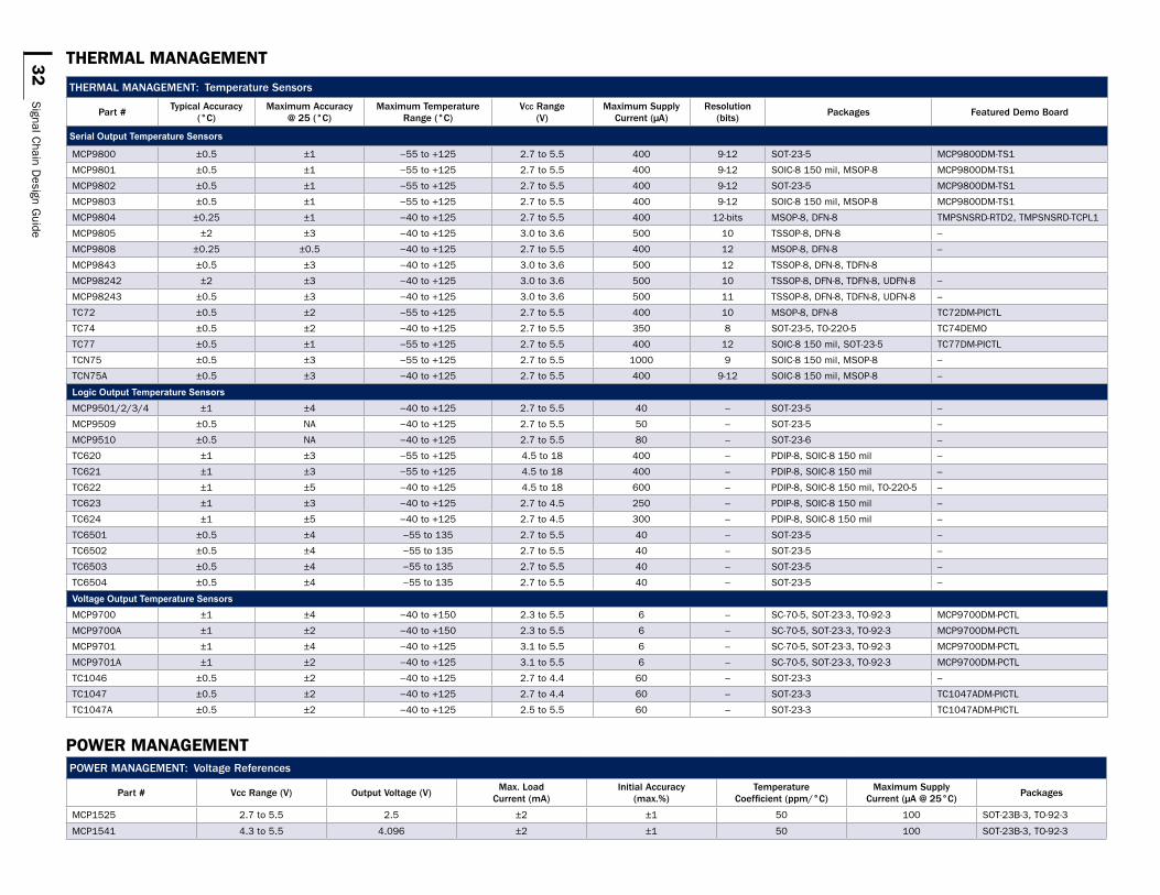
32
Signal C
hain Design G
uide
TherMal ManageMenT
THerMaL ManaGeMenT: Temperature Sensors
Part #Typical accuracy
(°C)Maximum accuracy
@ 25 (°C)Maximum Temperature
range (°C)Vcc range
(V)Maximum Supply
Current (µa)resolution
(bits)Packages Featured Demo Board
Serial Output Temperature Sensors
MCP9800 ±0.5 ±1 −55 to +125 2.7 to 5.5 400 9-12 SOT-23-5 MCP9800DM-TS1
MCP9801 ±0.5 ±1 −55 to +125 2.7 to 5.5 400 9-12 SOIC-8 150 mil, MSOP-8 MCP9800DM-TS1
MCP9802 ±0.5 ±1 −55 to +125 2.7 to 5.5 400 9-12 SOT-23-5 MCP9800DM-TS1
MCP9803 ±0.5 ±1 −55 to +125 2.7 to 5.5 400 9-12 SOIC-8 150 mil, MSOP-8 MCP9800DM-TS1
MCP9804 ±0.25 ±1 −40 to +125 2.7 to 5.5 400 12-bits MSOP-8, DFN-8 TMPSNSRD-RTD2, TMPSNSRD-TCPL1
MCP9805 ±2 ±3 −40 to +125 3.0 to 3.6 500 10 TSSOP-8, DFN-8 –
MCP9808 ±0.25 ±0.5 −40 to +125 2.7 to 5.5 400 12 MSOP-8, DFN-8 –
MCP9843 ±0.5 ±3 −40 to +125 3.0 to 3.6 500 12 TSSOP-8, DFN-8, TDFN-8
MCP98242 ±2 ±3 −40 to +125 3.0 to 3.6 500 10 TSSOP-8, DFN-8, TDFN-8, UDFN-8 –
MCP98243 ±0.5 ±3 −40 to +125 3.0 to 3.6 500 11 TSSOP-8, DFN-8, TDFN-8, UDFN-8 –
TC72 ±0.5 ±2 −55 to +125 2.7 to 5.5 400 10 MSOP-8, DFN-8 TC72DM-PICTL
TC74 ±0.5 ±2 −40 to +125 2.7 to 5.5 350 8 SOT-23-5, TO-220-5 TC74DEMO
TC77 ±0.5 ±1 −55 to +125 2.7 to 5.5 400 12 SOIC-8 150 mil, SOT-23-5 TC77DM-PICTL
TCN75 ±0.5 ±3 −55 to +125 2.7 to 5.5 1000 9 SOIC-8 150 mil, MSOP-8 –
TCN75A ±0.5 ±3 −40 to +125 2.7 to 5.5 400 9-12 SOIC-8 150 mil, MSOP-8 –
Logic Output Temperature SensorsMCP9501/2/3/4 ±1 ±4 −40 to +125 2.7 to 5.5 40 – SOT-23-5 –
MCP9509 ±0.5 NA −40 to +125 2.7 to 5.5 50 – SOT-23-5 –
MCP9510 ±0.5 NA −40 to +125 2.7 to 5.5 80 – SOT-23-6 –
TC620 ±1 ±3 −55 to +125 4.5 to 18 400 – PDIP-8, SOIC-8 150 mil –
TC621 ±1 ±3 −55 to +125 4.5 to 18 400 – PDIP-8, SOIC-8 150 mil –
TC622 ±1 ±5 −40 to +125 4.5 to 18 600 – PDIP-8, SOIC-8 150 mil, TO-220-5 –
TC623 ±1 ±3 −40 to +125 2.7 to 4.5 250 – PDIP-8, SOIC-8 150 mil –
TC624 ±1 ±5 −40 to +125 2.7 to 4.5 300 – PDIP-8, SOIC-8 150 mil –
TC6501 ±0.5 ±4 −55 to 135 2.7 to 5.5 40 – SOT-23-5 –
TC6502 ±0.5 ±4 −55 to 135 2.7 to 5.5 40 – SOT-23-5 –
TC6503 ±0.5 ±4 −55 to 135 2.7 to 5.5 40 – SOT-23-5 –
TC6504 ±0.5 ±4 −55 to 135 2.7 to 5.5 40 – SOT-23-5 –
Voltage Output Temperature SensorsMCP9700 ±1 ±4 −40 to +150 2.3 to 5.5 6 – SC-70-5, SOT-23-3, TO-92-3 MCP9700DM-PCTL
MCP9700A ±1 ±2 −40 to +150 2.3 to 5.5 6 – SC-70-5, SOT-23-3, TO-92-3 MCP9700DM-PCTL
MCP9701 ±1 ±4 −40 to +125 3.1 to 5.5 6 – SC-70-5, SOT-23-3, TO-92-3 MCP9700DM-PCTL
MCP9701A ±1 ±2 −40 to +125 3.1 to 5.5 6 – SC-70-5, SOT-23-3, TO-92-3 MCP9700DM-PCTL
TC1046 ±0.5 ±2 −40 to +125 2.7 to 4.4 60 – SOT-23-3 –
TC1047 ±0.5 ±2 −40 to +125 2.7 to 4.4 60 – SOT-23-3 TC1047ADM-PICTL
TC1047A ±0.5 ±2 −40 to +125 2.5 to 5.5 60 – SOT-23-3 TC1047ADM-PICTL
Power ManageMenTPOWer ManaGeMenT: Voltage references
Part # Vcc range (V) Output Voltage (V)Max. Load
Current (ma)initial accuracy
(max.%)Temperature
Coefficient (ppm/°C)Maximum Supply
Current (µa @ 25°C)Packages
MCP1525 2.7 to 5.5 2.5 ±2 ±1 50 100 SOT-23B-3, TO-92-3
MCP1541 4.3 to 5.5 4.096 ±2 ±1 50 100 SOT-23B-3, TO-92-3
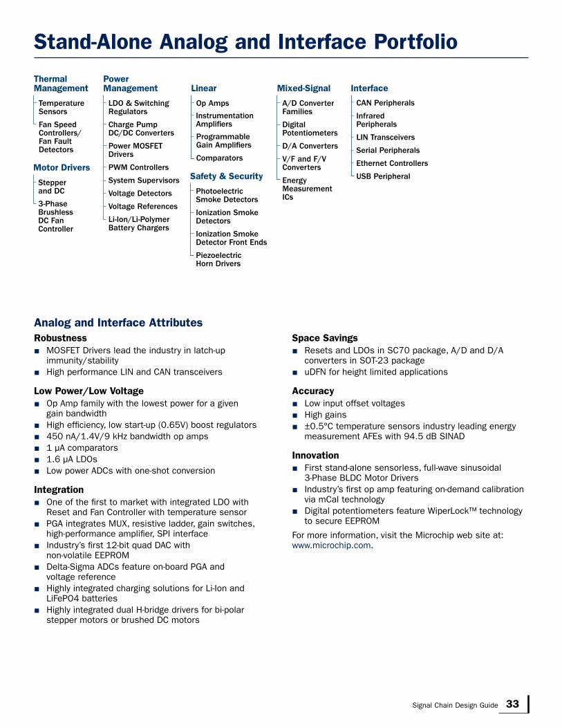
33Signal Chain Design Guide
Thermal Management
PowerManagement
TemperatureSensors
Fan SpeedControllers/Fan FaultDetectors
LDO & SwitchingRegulators
Charge PumpDC/DC Converters
Power MOSFETDrivers
PWM Controllers
System Supervisors
Voltage Detectors
Voltage References
Li-Ion/Li-PolymerBattery Chargers
Mixed-Signal
A/D ConverterFamilies
Digital Potentiometers
D/A Converters
V/F and F/VConverters
EnergyMeasurementICs
Interface
CAN Peripherals
InfraredPeripherals
LIN Transceivers
Serial Peripherals
Ethernet Controllers
USB Peripheral
Linear
Op Amps
ProgrammableGain Amplifiers
Comparators
Safety & Security
PhotoelectricSmoke Detectors
Ionization SmokeDetectors
Ionization SmokeDetector Front Ends
PiezoelectricHorn Drivers
InstrumentationAmplifiers
Motor Drivers
Stepper and DC
3-PhaseBrushlessDC FanController
Robustness MOSFET Drivers lead the industry in latch-up
immunity/stability High performance LIN and CAN transceivers
Low Power/Low Voltage Op Amp family with the lowest power for a given
gain bandwidth High efficiency, low start-up (0.65V) boost regulators 450 nA/1.4V/9 kHz bandwidth op amps 1 µA comparators 1.6 µA LDOs Low power ADCs with one-shot conversion
Integration One of the first to market with integrated LDO with
Reset and Fan Controller with temperature sensor PGA integrates MUX, resistive ladder, gain switches,
high-performance amplifier, SPI interface Industry’s first 12-bit quad DAC with
non-volatile EEPROM Delta-Sigma ADCs feature on-board PGA and
voltage reference Highly integrated charging solutions for Li-Ion and
LiFePO4 batteries Highly integrated dual H-bridge drivers for bi-polar
stepper motors or brushed DC motors
Space Savings Resets and LDOs in SC70 package, A/D and D/A
converters in SOT-23 package uDFN for height limited applications
Accuracy Low input offset voltages High gains ±0.5°C temperature sensors industry leading energy
measurement AFEs with 94.5 dB SINAD
Innovation First stand-alone sensorless, full-wave sinusoidal
3-Phase BLDC Motor Drivers Industry’s first op amp featuring on-demand calibration
via mCal technology Digital potentiometers feature WiperLock™ technology
to secure EEPROM
For more information, visit the Microchip web site at: www.microchip.com.
Analog and Interface Attributes
Stand-Alone Analog and Interface Portfolio

Microchip Technology Inc. 2355 W. Chandler Blvd.
Chandler, AZ 85224-6199
www.microchip.com
AMERICASAtlanta Tel: 678-957-9614Boston Tel: 774-760-0087Chicago Tel: 630-285-0071Cleveland Tel: 216-447-0464Dallas Tel: 972-818-7423Detroit Tel: 248-538-2250Indianapolis Tel: 317-773-8323Los Angeles Tel: 949-462-9523Santa Clara Tel: 408-961-6444Toronto Mississauga, Ontario Tel: 905-673-0699
EUROPEAustria - Wels Tel: 43-7242-2244-39Denmark - Copenhagen Tel: 45-4450-2828France - Paris Tel: 33-1-69-53-63-20Germany - Munich Tel: 49-89-627-144-0Italy - Milan Tel: 39-0331-742611Netherlands - Drunen Tel: 31-416-690399Spain - Madrid Tel: 34-91-708-08-90UK - Wokingham Tel: 44-118-921-5869
ASIA/PACIFICAustralia - Sydney Tel: 61-2-9868-6733China - Beijing Tel: 86-10-8569-7000China - Chengdu Tel: 86-28-8665-5511China - Chongqing Tel: 86-23-8980-9588China - Hangzhou Tel: 86-571-2819-3187China - Hong Kong SAR Tel: 852-2401-1200China - Nanjing Tel: 86-25-8473-2460China - Qingdao Tel: 86-532-8502-7355China - Shanghai Tel: 86-21-5407-5533China - Shenyang Tel: 86-24-2334-2829China - Shenzhen Tel: 86-755-8203-2660China - Wuhan Tel: 86-27-5980-5300China - Xiamen Tel: 86-592-2388138China - Xian Tel: 86-29-8833-7252China - Zhuhai Tel: 86-756-3210040
Sales Office ListingASIA/PACIFICIndia - Bangalore Tel: 91-80-3090-4444India - New Delhi Tel: 91-11-4160-8631India - Pune Tel: 91-20-2566-1512Japan - Osaka Tel: 81-6-6152-7160Japan - Yokohama Tel: 81-45-471- 6166Korea - Daegu Tel: 82-53-744-4301Korea - Seoul Tel: 82-2-554-7200Malaysia - Kuala Lumpur Tel: 60-3-6201-9857Malaysia - Penang Tel: 60-4-227-8870Philippines - Manila Tel: 63-2-634-9065Singapore Tel: 65-6334-8870Taiwan - Hsin Chu Tel: 886-3-5778-366Taiwan - Kaohsiung Tel: 886-7-2137828Taiwan - Taipei Tel: 886-2-2500-6610Thailand - Bangkok Tel: 66-2-694-1351
11/29/11
TrainingIf additional training interests you, then Microchip can help. We continue to expand our technical training options, offering a growing list of courses and in-depth curriculum locally, as well as significant online resources – whenever you want to use them.
Technical Training Centers: www.microchip.com/training MASTERs Conferences: www.microchip.com/masters Worldwide Seminars: www.microchip.com/seminars eLearning: www.microchip.com/webseminars Resources from our Distribution and Third Party Partners
www.microchip.com/training
SupportMicrochip is committed to supporting its customers in developing products faster and more efficiently. We maintain a worldwide network of field applications engineers and technical support ready to provide product and system assistance. In addition, the following service areas are available at www.microchip.com:
Support link provides a way to get questions answered fast: http://support.microchip.com and www.microchip.com/maps
Sample link offers evaluation samples of any Microchip device: http://sample.microchip.com
Forum link provides access to knowledge base and peer help: http://forum.microchip.com
Buy link provides locations of Microchip Sales Channel Partners: www.microchip.com/sales
Information subject to change. The Microchip name and logo, the Microchip logo, dsPIC, MPLAB and PIC are registered trademarks and PICDEM, PICtail and mTouch are trademarks of Microchip Technology Incorporated in the U.S.A. and other countries. © 2012 Energizer. Energizer and other marks are trademarks owned by Energizer. All other trademarks mentioned herein are property of their respective companies. © 2012, Microchip Technology Incorporated. All Rights Reserved. Printed in the U.S.A. 9/12 DS21825G
*DS21825G*