Typical Signal chain solutions for Industrial
67
1 Typical Signal chain solutions for Industrial
Transcript of Typical Signal chain solutions for Industrial

1
Typical Signal chain
solutions for Industrial

2
Agenda
• Industrial Signal Chain Overview
• Industrial Signal Conditioning and Acquisition
– Unipolar Signal
– Bipolar Signals
– Multi-Channel Signal
• Industrial Signal Transmission
– 4~20mA

3
Industrial Process Control
SIEMENS
6SE7016-1EA30WR 2,2 kWNr. 467321
SIMOVERT SC
Analog sensors
& actuators
(4 - 20mA)
Valves
Drives
HMI
Analyzer
Analyzer
Starters
DP / PA
Link
DCS
HART or
PA I/O
Instruments
Instruments
PLCPC
Simple binary
sensors & actuators
DP/ASI
I/F
Analog sensors
& actuators

4
OP
AMP
MUX FILTER A/D
C
or
P
D/APOWER
AMP
REF
TI Offers the Complete Signal Processing Chain
Anti-Alias Filter
Band-pass Filter
Programmable Gain Amp
Instrumentation Amp
A/D Converter Driver
Sensor Interface
Voltage Reference Source
Buffer
Gain
Difference Amplifier
Instrumentation Amplifier
Filter
Level Shift
Voltage Reference Source
Actuator Driver
Line Driver
4-20mA Driver
Voltage Reference Source
DDS Synthesis
Valve

5
Unipolar Signal Conditioning and
Acquisition

6
One of Sensors: Bridge Sensor
Vcc
Vout
Bridge
Measure the Followings:
• Pressure
• Temperature
• Humidity
• Acceleration
• Torque

7
Characteristic
Resistance-
Temperature
Detector (RTD)
Thermistor Thermocouple (TC) Integrated Circuit
Sensor
Temperature Range -70ºC to 500ºC 0ºC to 100ºC -270ºC to 1820ºC -40ºC to 150ºC
Linearity High (limited) Low (Non Linear) Non- linear Very Linear
Power Consumption External
Current/Voltage
Source
External Current
Source
Self Power System Power
(uA)
Output Range 100 to 1kΩ 100 to 40MΩ Low Voltage (mv) Digital Output
Self Heating Yes Yes No Yes
Sensitivity Low : +0.4Ω/° High: -3.9% /°C to
-6.4% /°C
10uV /°C
Very Low
0.5 °C
Operation 2-4Wire, Signal
Conditioning
2 Wire, Signal
Conditioning
Cold Junction
Compensation +
Signal Amplifier
Power Supply,
Self Contained
Temperature Measurement Sensors

8
Temperature: Why an RTD?
Table Comparing Advantages and Disadvantages of Temp Sensors

9
• Low Quiescent Current: 25µA (max)
• Low Offset Voltage: 10µV (max)
• Offset Voltage Drift: 0.05µV/˚C (max)
• Low Voltage Noise: 1.1 µVP-P
• Bandwidth: 350kHz
• Rail-to-Rail Input and Output
• 1.8V to 5.5V Supply Voltage
• Specified Temperature Range:
• -40°C to +125°C
• OPA333: SC70-5, SOT23-5, SO-8
• OPA2333: QFN-8, SO-8
OPA333, OPA2333Micro Power, Zerø-Drift Operational Amplifier
• Battery-Powered Instruments
• Temperature Measurement
• Precision Strain Gages
• Precision Sensor Applications
• Handheld Test Equipment
• Lowest Power Increases Battery Life
• Low Offset and Drift Removes Need for
Calibration in Application
• RRIO Increases Dynamic Range
• 1.8V Supply Excellent for Battery Devices
• Micro SC70 Package Saves Board Space
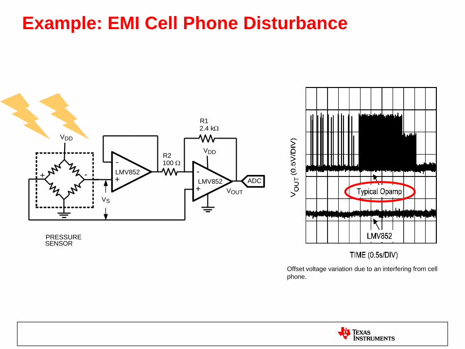
Offset voltage variation due to an interfering from cell
phone.
SENSOR
+ -+
-
ADC
PRESSURE
+
-
R1
R2100
2.4 k
VDD
VDD
VS
LMV852
LMV852
VOUT
Example: EMI Cell Phone Disturbance

Performance Improvement by EMI hardened
Amplifier
Given:
• Disturbing RF = 100 mVp at
900 MHz
• Op amp gain = 101x
• ADC: 10-bit resolution, 5V
input range -> 1 bit = 4.88 mV
Typical LMV851
EMI hardened
EMIRR 50 dB 80 dB
Input referred voltage shift 0.32 mV 10 V
Output shift 32 mV 1 mV
Signal path inaccuracy due EMI 7 bit 0.2 bit only

LMV851
LMV852
LMV854
LMV861
LMV862
BW = 8 MHz EMIRR = 87 dB
BW = 30 MHz
EMIRR = 105 dB Is = 2.25 mA per
channel
Is = 0.4 mA per channel
LMV831
LMV832
LMV834
BW = 3 MHz EMIRR = 120 dB
Is = 0.24 mA per channel
EMI Hardened Product Family
LMP2021
LMP2022
Zero Drift Low Noise
Amplifier

TI Confidential – NDA Restrictions
Key Advantages of the 24-bit AFEsLMP90100 and ADS1248
• Sample rate up to 2k SPS
• Integrated Reference
• Internal VBIAS
• Flexible internal routing of IBIAS
• Continuous Background
Calibration Engine (no drift over time
or temperature)
• Non-invasive Sensor Diagnostics
• Robust Data Transmission (CRC)
VA
CLK/XIN
CSB
SCLK
SDI
SDO
VREF1
VIN0
VIN1
VIN2
VIN3
VIN4
VIN5
IB1
IB2
VA
RANGE
SETTING
GND
Gain
1x to 128x
GPIO
D6 D0
SENSOR
DIAGNOSTICS
VIORANGE
SETTING
SERIAL
INTERFACE
POR
24-bit SD
MODULATORDIGITAL
FILTER
MUX
PGA
VIN6
BACKGROUND
CALIBRATION
VIN7
VREF
MUX INTERNAL
CLOCK
FL
EX
IBL
E M
UX

TI Confidential – NDA Restrictions
Product Comparison
Key Specifications LMP90100 Family ADS1248 Family
Fully Integrated AFE
Single Cycle Settling Time
Flex Routing of Inputs
Self-Calibration Continuous Background
and System
System Calibration
Sensor Diagnostics (Non-invasive)
Serial Interface SPI with Error Detection SPI
Variable Data Rate Up to 214 SPS Up to 2k SPS
Power Consumption 400 µA 230 µA
ENOB 21.5 bits 21.8 bits
Analog Supply Voltage 2.85V to 5.5V 2.7V to 5.25V
Small form factor TSSOP - 28 TSSOP – 28
Operating Temperature -40°C to 125°C -40°C to 125°C

15
ADS1247/4824-Bit, Complete Temperature Measurement ADC
EVM
• Ultimate Temperature Sensor Measurement Solution
• Most Flexible Front End for a Wide Range of Industrial Sensors
• High Integration Without Compromising Performance
• Scalable Upgrades
Device Features:• 2/4 Differential or 3/7 Single-Ended
• True Bipolar ± 2.5V or Unipolar 5V
• Max Data Rate – 2kSPS
• Low Noise PGA: 40ηV @ G = 128
• 50/60Hz Simultaneous Rejection Mode (20SPS)
On-Chip Integration:• Low Drift Internal Reference (10 ppm/ Max)
• Dual Matched Current DACs (50 – 1500 μA)
• Oscillator, Temp Sensor, Burnout Detect
• 4/8 General Purpose I/Os
• 16-Bit Upgrade upcoming ADS1147/48
• Temperature Management – RTDs, Thermocouples, Thermistors
• Flow/Pressure Measurement
• Industrial Process Control
EVM:ADS1248EVM 20/28-Pin TSSOP

16
3-Wire RTD Measurement

EVM PART # LMP90100EB
24-Bit Low Power Sigma Delta ADC
4 Diff or 7 SE inputs (mix and match)
True Continuous Background Calibration and
Background Diagnostics at all gains
Low-Noise 1x to 128x PGA
Part of Pin - Compatible Family
LMP90100 supported with Web Design Tool and
Bench-top Development System
Single board layout supports multiple resolutions
and Configurations
Performance stated for each gain/speed
combination (Web Design tool and datasheet)
Very Low Power
Transducers and Transmitters
RTD, Thermocouple, Temperature Sensors
Pressure, Load and Force Sensing
Data Acquisition
LMP90100Multi-Channel, Low Power 24-Bit Sensor AFE withTrue Continuous Background Calibration
Resolution Current Sources 4 Diff. / 7SE 2 Diff. / 4SE
24 Bit Yes LMP90100 LMP90098
24 Bit No LMP90099 LMP90097
16 Bit Yes LMP90080 LMP90078
16 Bit No LMP90079 LMP90077Micrcontroller
RREF
3-wire
RTD
+
VREF
--
PressureSensor
VA
CLK/XIN
CSB
SCLK
SDI
SDO
VREF1
VIN0
VIN1
VIN2
VIN3
VIN4
VIN5
IB1
IB2
VA
RANGE
SETTING
GND
Gain
1x to 128x
GPIO
D6 D0
SENSOR
DIAGNOSTICS
VIORANGE
SETTING
SERIAL
INTERFACE
POR
24-bit SD
MODULATORDIGITAL
FILTER
MUX
PGA
VREFP2
BACKGROUND
CALIBRATION
VREFN2
VREF
MUX INTERNAL
CLOCK
FL
EX
IBL
E M
UX
Configuration
Input
Signal Path
Output / External

Continuous Calibration Advantages
• Primary benefit of continuous calibration is excellent drift compensation
for both drift components
– Drift over temperature
– Drift over time
• Current methods for compensating for drift are:
– Chopping for offset drift
– Monitoring the temperature and re-calibrating if temperature changes
– Budgeting drift error in system errors and re-calibrating at fixed time
intervals
• None of the existing methods are perfect for drift compensation.
Continuous calibration offers the best results

19
Background Offset Correction
• Offset Estimation:
– Alternate input samples to the ADC are inverted and the two digital
output codes are averaged
• Offset Correction:
– All the subsequent conversions can use cest to eliminate the offset
• cest is continuously updated to eliminate drift errors
212/21
2.2
1.1
xxifyyc
cxAy
cxAy
est

Offset Error without Background Calibration

Offset Error with Background Calibration

22
Background Gain Correction
• Gain Estimation:
– A known value Dx is added to alternate analog input samples and the
difference between the digital codes is used to estimate the gain
• Gain Correction:
– All the subsequent conversions can use A'est to eliminate the gain error
• A'est is continuously updated to eliminate drift errors
xxxifxyyA
cxAy
cxAy
est DD
12/12
2.2
1.1

Background System Calibration
Two separate 24-bit registers for Gain & Offset Correction factors
User has read & write access to these registers
System Offset.Register
System Offset
Calibrated O/P
System Gain.Register
X
SystemGain,Offset
CalibratedADC
Vin Background
Calibration
Background
Gain, Offset
Calib. O/PO/P

Sensor Diagnostics – What is required
– Comprehensive solution to detect various fault conditions
– Should work for various sensors (RTD, Thermistors, Thermocouple)
– Should work for various configurations (2,3,4 wire)
– Provide information about possible cause of failure.
– Background no User intervention required.
– Continuous, monitors all the time
– Should not interfere with the input
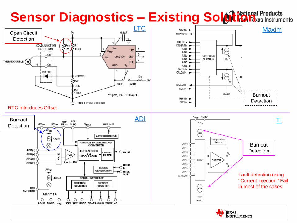
Sensor Diagnostics – Existing SolutionLTC
Open Circuit
Detection
RTC Introduces Offset
ADI
Maxim
TIBurnout
Detection
Fault detection using
“Current injection” Fail
in most of the cases
Burnout
Detection
Burnout
Detection

Sensor Diagnostics – Existing Solution• Issues with Current Injection:
– Can’t detect all the Fault conditions, only on demand
– Slows down the total conversion rate as ADC O/P is used.
– Interfere with the main measurement.
– Small current sources for open/short detection is not usable by
temperature transmitters. This is because RC filters are
connected to every input linked with the outside world need a lot
of time to charge the capacitor and is therefore not usable.
– Once enabled as shown below all the channels are effected.
Current injection is not channel specific.VIN0
VIN1
VIN2
VIN3

• Current Injection
– Helps to detect Floating inputs.
– Channel Specific Current Injection.
Current scan
Existing Solution Proposed Solution
From nA
to 10uA

28
• Single Channel Current Injection
Current scan modes
• Automated Scan injection.
– Current is not injected into the channel that is being evaluated.
– Idea is to minimize the interference with Signal.
CH1 CH2 CH3Frame-1: CH1 is Evaluated
Burnout Current Injection
CH1 CH2 CH3Frame-2: CH2 is Evaluated
CH1 CH2 CH3Frame-3: CH3 is Evaluated
CH1 CH2 CH3Frame-1: CH1 is Evaluated
Burnout Current Injection
CH1 CH2 CH3Frame-2: CH2 is Evaluated
CH1 CH2 CH3Frame-3: CH3 is Evaluated

Sensor Diagnostics – Advantages
Detection Method Interference to Input
Competitors National Existing Proposed
Shorted Input
Pump Burnout Current.
Change in Resistance
should store history .i.e C
RTD/TC: Same as Existing (Or)
Using of Threshold Register
[Window Comparison].
Yes Yes/ No
Floating Input
No Inject Burnout Current.
Near rail detect comparators detect
a Float.
NA No
Over Load
Detection
No With Modulator overflow detection
we can easily detect if input
exceed the allowed range. Also we
can detect if Reference is
open/short
NA No
• Multiple Methods to detect different kind of fault Conditions
• Burnout Current Source Scan.

30
ADS1118World’s Smallest 16-bit ADC, w/0.5ºC (max) Accurate Temp Sensor
•Complete set of integrated functions:
• Four multiplexed analog inputs
• Four digital I/O
• PGA (gains: 0.33, x0.5, x1, x2,
x4 or x8)
• Precision ADC with data rates from 8 to 860
SPS
• Internal temperature sensor (0.5ºC max)
• Small QFN package (2.05mm x 1.55mm x
0.4mm)
•Versatile supply range and low power consumption
• Low supply current: 150uA typ
• Supply 2.0V – 5.5V
• Temperature Measurement
• Battery Pack
• Portable Instrumentation
• Industrial Process Control
• Gas Monitoring
• Consumer Goods
• Embedded ADC Upgrade
CSn
DOUT/DRDYn
VDD
GND
SCLK
16-bit DS
ADCPGA
Oscillator
InternalReference
M
U
X
Gains:
2/3,1,2,4,8,16
DIN
Temp Sensor
AINP1
AINP0
AINP3
AINP2
SPI
Interface
Tiny QFN(RUG) or MSOP(DGS) Package
• A single ADS1118 can perform data acquisition of
multiple signals from a wide variety of sensors.
• Small package that readily senses ambient
temperature to perform cold junction compensation in
thermocouple applications.
• Its size and low power consumption make the
ADS1118 a great device for portable applications
where extended battery life is critical
ADS1118 EVM Available

31
• 250mV input voltage range
• Fixed gain: 8
• Gain error: 1% max; drift: ±40ppm/C
• Input bandwidth: 60kHz min
• Input offset voltage: 2mV max;
drift: ±10V/C max
• Non-linearity: ±0.05% max
• Transient immunity: 10kV/s min
• Specified Temp range: -40..105C
• Package: Gullwing-8
• Pin-to-pin performance upgrade for
HCPL7800 & HCPL7840
• 50% lower power dissipation on
VDD1
• Current measurement in: Motor Control
Isolated Power Supplies
AMC12004kVPEAK Isolated Amplifier
0V 250mV
2.55V 2V
1.3V 2V
5V:
3.3V:

32
32
Q
LMP91000 Application Diagram
Toxic Gas Sensor
I2C INTERFACE
AND
CONTROL
REGISTERS
RE
VREF VDD
AGND
CE
WE VOUT
C1
SCL
TEMP
SENSOR
VREF
DIVIDER
C2
SDA
RLoad
VARIABLE
BIASMENB
DGND
A1+
-
TIA+
-
RTIA
CE
WE
RE
3-Lead
Electrochemical
Cell
CONTROLLER
LMP91000

LMP91000 Product Overview
• Low Power (<10uA)
• TIA Gain ranges (KΩ) : 2.75, 3.5, 7, 14, 35, 120, 350, external
resistor
• Reference Electrode Bias Current: 900pA (max)
• Cell conditioning currents: up to 10mA
• Output Drive Current: > 750 uA
• Internal Temp Acc: +/- 3˚C
SpecificationsFeaturesCompetitive
PositionSensors

LMP91000 Product Overview
SpecificationsFeaturesCompetitive
PositionSensors
Area TIDiscrete
Solution
Single solution addresses multiple gases Χ
Small footprint Χ
One solution across multiple types of sensors Χ
One solution across varying gas concentration Χ
Integral Temperature Sensor Χ
Quick Design /Prototype evaluation Χ
Ease of Use Χ
System Reliability Improved -
Low Power Consumption Χ*
Superior EMI Protection Χ*
* Requires special op amps

EVM PART # LMP91000SDE/NOPB
Programmable transimpedance gain
Programmable cell bias voltage
Supply current (Average over time) <10uA
On board sensor test
On board temperature sensor
Low bias voltage drift
Operating supply range: 2.7V to 5.5 V
Cell conditioning currents up to 10mA
Reference Electrode Bias Current 1000pA (max)
Output Drive Current 670µA (min)
Sink and source capability
I2C® compatible digital interface
Industry’s low power complete potentiostat circuit which interfaces to
most of today’s single channel chemical cells. Programmability enables
A modular approach for our customers
One solution for multiple devices
Offers the proper amount of integration which makes smaller
solutions for the customer
Lower assembly and handling cost
And finally helps them get their products to market faster!
Toxic gas detection platforms
Amperometric applications
Chemical species detection
LMP91000Configurable AFE Potentiostat for Low-Power Chemical Sensing Applications

EVM PART # LMP91200EVAL
Complete integrated front end for pH sensing
Ultra low input bias current: 0.45 pA at 85°C
Programmable Output Common Mode Voltage
Active guard pins
Easy RTD hookup for temperature measurement
Supported by Webench Sensor AFE Designer
World’s first single chip solution helps reduce
design time, cost and board space
99% lower bias vs. competition allows reliable
measurement with high impedance pH electrodes
Provides flexibility to use with several pH sensor
output ranges
Provide high parasitic impedance wiring to
eliminate leakage
Allows calibration of temp. drifts over time
Online & Hardware evaluation tools enable quick
evaluation, prototyping and faster time to market
Low power consumption allows intelligent
sensors
pH Sensor Platforms
Chemical/Petrochemical Plants
Refining & Gas production
Emission Monitoring
Steam & Water quality monitoring
LMP91200Fully Integrated Analog Front End for pH Analyzer Sensor Platforms
1ku pricing=$4.50

37
37
Q
LMP91200 Application DiagrampH sensing
CSB
+
-
PGA
VDD
SCLK
SDI
VOUT
VOCM
VREF
SDO_DIAG
GND
VCMHI
VCM
GUARD2
INP
GUARD1
CAL
RTD
VCM
BUFFER
RangeSetting
LMP91200
SPI
pH ELECTRODE
CONTROLLER
2-wire RTD
R REF
pH
BUFFER
VOUT
MUX
VCM
MUX
High impedance CM
o/p if needed
Guard pins to prevent
leakage currents
Adjustable VCM: Vref/8 ,
2Vref/8 to 7Vref/8
Diagnostic features to
detect sensor and check
sensor connection
CM o/p for differential o/p
measurement
Excitation currents for
RTD: 100uA to 1mA
Through SPI , one can switch b/w
pH measurement mode and temp.
measurement mode
Precision resistor for high
accuracy temp. calibration
RTD input

38
Bipolar Signal Conditioning and Acquisition

39
OPA188 / OPA2188 / OPA41880.03µV/oC, 25µV Vos, 36V Zerø-DriftTM Operational Amplifier
Packaging options:
Single: SO-8, MSOP-8, SOT-23
Dual: SO-8, MSOP-8
Quad: SO-14, TSSOP-14
OPA188
1ku: $0.80
RTM 1Q’12
OPA2188
1ku: $1.40
RTM 8/2011
OPA4188
1ku: $2.45
RTM 4Q’11
• Very Low Offset and Drift• Offset Voltage: 25µV (max)• Offset Voltage Drift: 0.085µV/°C max• CMRR, PSRR, Aol = 130dB (min)
• Noise Voltage: 8.8nV/√Hz at 1kHz•GBW : 2MHz
• Low Quiescent Current: 475μA (max)• Low Bias Current: 160pA (typ)
• Supply Range: +4.0V to +36V or ±2V to ±18V• Rail to Rail Output• EMI/RFI Filtered Inputs
• Improved high accuracy and stability over the previous generation OPA277
• Offset drift 75% lower than the nearest competitor
• Allows for high sensitivity, high resolution systems across a wide frequency range
• Well suited for battery powered operation• Minimizes errors on the output due to current
noise• Flexibility in design, enabling low power 5V supply systems
• Improved Noise Immunity
• Electronic Weigh Scales• Bridge Amplifier• Strain Gauge• Automated Test Equipment• Transducer amplifier• Medical Instrumentation• Resistor Thermal Detector

TI:
OPA2171
TI:
OPA2188
TI:
OPA2277
ADI:
ADA4638
ADI:
OP2177
ADI:
AD8677
(single)
TI:
OP07C
Vmin 2.7V 4V 4V 5V 5V 8V 6V
Vmax 36V 36V 36V 30V 36V 36V 36V
Iq / channel (max) 595uA 475uA 825uA TBD 600uA 1.3mA 5mA
Vos (max) 1.8mV 25uV 25uV 10uV 60uV 130uV 150uV
Offset Drift (typ) 0.3uV/C 0.03uV/C 0.1uV/C 0.04uV/C 0.2uV/C 0.5uV/C 0.5uV/C
Ib (max) 15pA 850pA 1000pA TBD 2000pA 1nA 7nA
GBW (typ) 3MHz 2MHz 1MHz TBD 1.3MHz 600kHz 600kHz
Slew Rate (typ) 1.5V/us 0.8V/us 0.8V/us 2 0.7V/us 0.2V/us 0.3V/us
CMRR (min) 104dB 130dB 130dB 120dB 120dB 120dB 100dB
Vn @ 1kHz 14nV/√Hz 8.8nV/√Hz 8nV/√Hz 60nV/√Hz 7.9nV/√Hz 10nV/√Hz 9.8nV/√Hz
Rail to Rail Out Out NA Out NA NA NA
Package (Single) 8MSOP
8VSSOP
8SOIC
8MSOP
8SOIC
5SOT23
8PDIP
8SOIC
8DFN
8SOIC
8LFCSP
8MSOP
8SOIC
5SOT23
8SOIC
8SOIC,
8PDIP
Price @1ku $0.6 $1.40 $1.65 TBD $1.5 $0.76 $0.4
HV Low BW Amplifier – Competitive Analysis

411/12/11/sb 41
Newer Op-amps have built-in EMI filtering

42
OPA209, OPA2209, & OPA4209
Low Noise, Low Ib Op Amp with RRO in SOT23
• Improved Dynamic Range
• Lower Power Dissipation
• Space Savings
• Low Noise : 2.2nV/√Hz max
• 130nVpp Noise, 0.1Hz – 10Hz
• Low Ib: 12nA max
• Low Supply Current: 2.3mA/Amp max
• Low Offset Voltage: 100µV max
• Gain Bandwidth Product: 18MHz
• Slew Rate: 6V/µs
• Wide Supply Range ±2.25 to ±18V,
4.5 to 36V
• Rail-to-Rail Output
• Single - SOT23-5, MSOP-8, SO-8
• Dual – MSOP-8, SO-8
• Quad – TSSOP-14, QFN-16
• Pll Loop Filter
• Low Noise, Low Power Signal Processing
• High Performance ADC Driver
• High Performance DAC Output Amplifier.
• Active Filters
• Low Noise Instrumentation Amplifiers

43
OPA171, OPA2171, OPA4171
36 Volt SOT-563 Amplifier
• Transducer Amplifier
• Bridge Amplifier
• Temperature Measurements
• Strain Gauge Amplifier
• Precision Integrator
• Battery Powered Instruments
• Test Equipment
Precision
Stability
Clean Signal Conditioning
Single Supply Operation
Wide Common Mode Range
Improved Noise Immunity
Fast Response
Wide Signal sources
High Stability
Low Errors
Versatility
Battery Operation
Multi Channel Options
Smallest Board Footprint
• Offset Voltage: 2mV (max)
• Offset Voltage Drift: 3µV/°C
• Noise Voltage: 15nV/√Hz
• Input Range Includes the Negative Supply
• Input Range Operates to the Positive Supply
• RFI Filtered Inputs
• Slew Rate: 1.5V/µs
• GBW: 3 MHz
• High Common-Mode Rejection: 90dB
• Low Bias Current: 10pA (max)
• Supply Range: +2.7V to +36V, ±1.35V to ±18V
• Low Quiescent Current: 500μA (max)
• Single, Dual. Quad Versions
• MicroPackages: Single in SOT- 563, Dual in VSSOP-8
Small Size
SOT23-5
3 x 3 x 1.45
SC70-5
2 x 2 x 1.1
SOT-563
1.6 x 1.6 x 0.6
65%

• Maximum input signal range with a single device for
both single or bipolar supply industrial
applications
• Achieve precision measurement with high EMI
robustness.
• High performance on Low or High Vs
• DFN saves 30% of Space vs MSOP-8
• Wide Common Mode Input Range
• Input voltage swing V- to V+(-1V)
• +/-50V Input Protection
• Precision Input:
• Low Offset Voltage: 40uV
• EMI Hardened
• CMRR (G = 1): 84 dB min
• Input noise: 18 nV/√Hz
• Low Power and Wide Supply:
• Max supply current: 250 μA
• Supply: +2.7 to +36V, ±1.35V to ±18V
• Rail-to-Rail Output
• Standard and Micro Packages
• MSOP-8, SOIC-8, & SON-8 (3x3)
• Industrial process controls
• Circuit Breakers
• Current Measurement
• Medical instrumentation
• Portable data acquisition
INA826
INA826 Low Power RRIO Precision Instrumentation Amp

45
Multi-channel Signal Conditioning and
Acquisition

46
12-bit
ADC
Sw
itc
hin
g / M
ux ADSxxxx
Multi-Channel signal acquisition
BT
C
MSP430
USB
SD
BUTTON I/F
Amp
RS23
2
CF
Charge
r
PSUMonitor
Disp
Lamp
+
RTC
TMS320F28xxTMS320C5000
TLV2221TLV2264TLV2434OPA4348TLC2254+
-
+
-
+
-
+
-
+
-
+
-
+
-
+
-
x6
x6
x6
x6
x6
x6
x6
x6
TEMP1
VCC
TEMP2
GYRO
ACCEL
PRESSURE
VIBRATION
12-bit
ADC
ADS8201
+
-PGA
Co
ntr
ol an
d
SP
I
Ref
Sw
itc
hin
g / M
ux
Oscillator
FIFO
TEMP1
VCC
TEMP2
GYRO
ACCEL
PRESSURE
VIBRATION
Component Cost ~$5 to $10
Power Dissipation ~ 100mW
PWB Space ~ 1,000mm2
Component Count ~ 9
>75% Lower Power
>75% Less PWB Space
>75% Less Components
>75% Lower Cost

47
ADS8201Low Power, Low Cost, Multi-channel, 12-Bit, 100kHz, Data Acquisition System with Integrated PGA
• Portable Communications
• Transducer Interface• Portable Medical Instruments• GPS based applications• Sensor data acquisition systems
• Internal PGA-14 bit resolution for 12-bit cost!
• Conversion results can be saved and read
back later with the addition of an onboard
FIFO!
• Power and Board Space Savings all in one!
• No competition at such low power with such
integration
•Internal High-performance PGA (G=1,2,4,8)
•Bit Effective resolution up to 14-bits
•Gain/Channel mapping function. Specific
gains can be set for each channel selected for
conversion
•Onboard 8X1 FIFO
•Eight single ended/four differential channel MUX
onboard
•Iq (typ)=800uA
•Deep Power-Down Mode
•Excellent DC performance:
•INL : +/-1.5lsb; DNL : +/-1.0lsb
• Up to 100kHz throughput rate
•Vdd= 2.2 to 5V
•Iq (typ)=800uA
•24 pin, 4X4 QFN

48
• Single chip solution for wide range of inputs;
and direct interface with low voltage processors
without the need for level shifting
• Integration reduces system cost and complexity;
while threshold detection reduces the number of
accesses required by host processor in monitoring
applications
• Enables designers to change resolution without
redesigning their board or control software
• Industrial Process Controls (PLC)
• High-Speed Data Acquisition Systems
• High-Speed Closed-Loop Applications
• Digital Power Supply
ADS863812-Bit, 1MSPS, 8-Ch, True Bipolar, -power, serial, SAR ADC
• Flexible, Cost-Saving, Design• SW selectable input ranges selection
± 10, ± 5, ± 2.5V, 0-5V,0-10V
• Wide Digital Supply 1.65 to 5.25V
• Integration and Precision• Internal reference and temperature sensor
• Two programmable alarm thresholds / channel
• Alarm / temp threshold output
• Small Footprint Product Family• Pin compatible with ADS7951
• SPI Serial Interface
• 4x4 QFN
• -40 to 125 Specified Temperature Range
EVM Available
MUX
SPI
AIN0
AGND
AVDD DVDDREF
REF
HVDD
HVSS
°C
Threshold
Compare AL_PD
CS, SCLK,
DIN, DOUT
DGND
AINGND
ADC
REFGND
AIN1
AIN2
AIN3
AIN4
AIN5
AIN6
AIN7
ADS8638

49
• Low Power
• Automatic
• Small Size, 4X4 QFN package• High Speed SPI Serial Interfaces
• Compatible Upgrade/Downgrade paths
• 16 SCLK cycle (comparing to ADS8344)
• Scan Range Select
• Daisy Chain
• Programmable Status Output
ADS8331/3216-bit, 500KSPS, 4/8 Channel Serial SAR ADCs in QFN
• GPS Sensor Conditioning
• Portable Data Logging with multiple Inputs
• Battery Powered Equipment (i.e.. PDA, PCA, Cellular)
• Isolated Data Acquisition
• Transducer Interface
CH[0:3]
VREF
CONVST-
SDI
FS/CS-
SCLK
SDO
+
-CDAC
SAR
COMPARATOR
OUTPUT
LATCHES
&
TRI-STATE
DRIVERS
CONVERSION
&
CONTROL
LOGICCOM RESET-
M
U
X
MUXOUT ADCIN
Or CH[0:7]
OSC
Temp
Sensor
EOC/INT-
/CDI
Low power, flexible supply range o 2.7V~5.5V Analog Supply o Only 6.75mW (250KHz,+VA=2.7V, VBD=1.8V) o Only 10mW (500KHz,+VA=2.7V, VBD=1.8V)
Up to 500KHz Sampling Rate
Excellent DC Performance o ±1.2LSB TYP, ±2LSB MAX INL o ±1LSB TYP, -1.5/+2LSB MAX DNL o 16 Bit NMC Over Temperature o ±0.5mV Offset Error @ 2.7V o ±1mV Offset Error @ 5V
Excellent AC Performance @fi=10KHz o 91dB SNR o 100dB SFDR o -96dB THD
Flexible analog input arrangement o Unipolar Input Range 0 ~Vref o Onchip 4/8 channel MUX with breakout o Auto/Manual channel select & trigger
Other built hardware features o Onchip Conversion clock (CCLK) o Hardware/Software Reset o Onchip temperature sensor o Programmable Status/polarity EOC/INT-
Multi-Chip ready and fully automated o Daisy Chain Mode o Programmable Tag Bit Output o Global CONVST- (Independent of CS-)
Friendly I/O o SPI/DSP Compatible Serial interface o Separate I/O Supply 1.65V~1.5*(+VA) o SCLK up to 50MHz
Comprehensive Powerdown Modes: o DEEP Power-down o NAP Power-down o AUTONAP Power-down
24 Pin 4X4 QFN & TSSOP Packages

50
ADS855616-Bit, 630/450kSPS, 6ch Simultaneous Sampling SAR w/ Bipolar Inputs
• Best In Class AC/DC Performance
• 16-Bit, 3 LSB MAX INL
• 91.5db SNR (typ)
• True bipolar inputs with software selectable input ranges
up to ±12V and Selectable parallel or serial interface
• Pin Compatible 14 -/12-Bit Versions
• LQFP-64 Package pin compatible with AD7656
• Only 122mW @ 250kSPS
• Excellent performance and external conversion clock for
synchronization of multiple devices enables flexible and
expandable systems
• Allows easy connectivity to a wide range of inputs ,
sensors, and host processors
• Allows for an easy upgrade / downgrade path for future
designs
• Improved second source to ADI device with >2x faster
sampling rate and 3.5db better SNR
• Power quality and automation
• Protection relays
• Closed loop servo control
• Robotics

5151
ADS856816-Bit, 500/400kSPS, 8-ch Simultaneous Sampling SAR w/ Bipolar Inputs
• 8 True bipolar inputs support up to ±12V
• Small, Integrated Industrial Solution
• 2.5V programmable reference
• Fully specified from -40 to 125°C
• QFN-64 & TQFP-64 Packages
• Supports internal and external conversion clock
• Supports parallel and serial data interface
• Pin Compatible 14-/12-Bit Versions
• 600/450kSPS @ 14-bits
• 650/480kSPS @ 12-bits
• Power Automation:
Protection Relays
Power performance measuring and
monitoring devices (PMD)
• Multiphase Motor Control
• Multi-axis positioning systems
• Industrial automation and Data Acquisition
Control
&
I/O
REF2.5V
ADC 8
REFIO
CTRL
AVDD DVDD
CONFIG
register
S/HADC 1
10bit
DAC
HVDD HVSS
SER
or
PAR
DATA
ADC 2
ADC 3
ADC 4
ADC 5
ADC 6
ADC 7
S/H
S/H
S/H
S/H
S/H
S/H
S/H
CHA0
CHA1CHB0
CHB1CHC0
CHC1CHD0
CHD1
AGND
AGND
AGND
AGND
• Enables 20% wider voltage input range than competing
devices resulting in easy connectivity to a wide range of
inputs and sensors
• External conversion clock for synchronization of multiple
devices enables flexible and expandable systems at up
to 500kSPS for parallel and 400kSPS serial interfaces
• Easy upgrade / downgrade path for all designs

52
Industrial Signal Transmission

53
Industrial Signal Transmission Approach
RL
Noise
RWIRE
RWIRE
RWIRE
RWIRE
RWIRE
RWIRE
RWIRE
Noise
4mA = 0% level
20mA = 100% outputNoise
<4mA can flag Fault Conditions
>20mA can flag Fault Conditions
Option 1 Option 2
Option 3

54
Why Use Current Transmitters?
• Immunity to noise (50/60Hz)
– Industrial locations can make voltage transmission
unusable
– Unknown noise sources in between transmitter and
receiver
• Long distance transmission
– Distance determined by supply and loads present on
communication line
– Transmission distance can reach several miles based
on application conditions

55
4-20mA Overview
SensorReceiver
250Ω
0 to 100%
Signal
4 to 20mA
Signal
Transmitter 1V to 5V
• 4mA represents 0% input level
– Allows up to 4mA to power external input circuitry
– 4mA zero level allows underscale settings and fault detection
• 20mA represents 100% input level
– Provides sufficient current to power electromechanical devices
– Overscale can also be used to detect fault conditions

56
Transmitter Type Diagrams
RL VOUTXTR+VS
IOUT4-20mA
>1000 feet
-
+
250 typ 1V-5V typ
+24V Typical
+7V to +44V50 - 60 Hz
Noise
Two-Wire Transmitter
Three-Wire Transmitter
VLOOP
RL
+8 V to +40V
+24 V typical
VOUT
XTR
+VS
IOUT4-20mA
> 1000 feet
-
+
250 typ 1V-5V typ
50-60 Hz Noise

57
2-Wire vs. 3-Wire Transmitter
• 2-Wire Transmitter (Receiver powered)
– Referred to as Loop Powered
– Transmitter and sensor remotely located
– Local power supply not practical
– Input circuitry floats with respect to loop supply ground
• 3-Wire Transmitter (Transmitter powered)
– Referred to as Locally Powered
– Transmitter located close to power supply
– Input is referenced to power supply ground
– Also referred to as voltage to current converters

58
Implementation Of Current Transmitters
°T
XTR
XT
R
3-Wire
XTR111
2-Wire
XTR112
RL
• 2-Wire Transmitter
– Submersible temperature
sensor
– Remote location prevents
local power supply
– Sends data back to control
station
• 3-Wire Transmitter
– Sends control signal to
element at remote location
– Local power supply is
available

59
XTR117 Typical Input Scaling (2 Wires)
• 4-20mA span is 16mA
• XTR117 has current gain
of 100
• Input span is 160uA
• Offset needed if input
signal reaches zero
+
-
XTR117
R1
IIN
IRET
A1
2
3
8 VREG
IO = 100 * IIN
2.475 kΩ
+5V
40uA
0 to 160μA
12
5kΩ
IIN
Offset
Current

60
XTR117 Typical Input Interface
XTR117
IIN
IRET
2
3
8
VREG
IOUT DAC
XTR117
IIN
IRET
2
3
8
VREG
VOUT DAC
XTR117
IIN
IRET
2
3
8
VREGREF3140
Input
Circuitry

61
+
-
XTR111 OD
A1
GND
VSP
+
-
Current
Mirror
+
-
EF
ISET
+24V
REG F
SREG
3V
REF3140
VIN
VOUT DACμC
+5V
2kΩ
3kΩ
47
0n
F
2kΩRSET
15Ω
LOAD
15Ω
Q1
Q2
VG
IS
10
nF
Short-Circuit
Protection
XTR111 Typical Input Interface (3 Wire)

DAC161P997 16bit DAC with Single Wire Interface and “4-20mA” current loop drive
1ku pricing = $4.00
16 bit DAC Low Power Single Wire Interface (SWI), with handshake Programmable start up condition Self adjusts over wide baud rate range Error detection and reporting Programmable output Error Level Auxiliary HART input Internal Reference
4to20mA loop transmitter platforms 2-wire sensor systems
Process Control Factory automation Building automation
Fully Integrated Solution with well defined specification Easy reuse of design & reduces logistics cost No additional high accuracy components needed
Satisfies system needs of total power consumption < 30mW
SWIF interface – saves upto 3 digital isolators SWIF interface – low noise Defined Start-Up Condition 3.375mA or 21.75mA & pin
programmable Flexible update-rate/power-consumption trade-off Automatic detection of error conditions

Competitive Information
Single Wire Interface NO Yes Saves 2 or 3 digital isolators
Diagnostics NO Yes Enhances system reliability
Start Up Condition Yes Yes Better
Total TC Typ Numbers
Only
29ppm/'c max Acheives higher system
accuracy w ith user
calibration of offset & gain
HART Interface No Yes HART input to chip eliminates
need of external mixing
Total Size 60mm2 30mm2 Reduces system size
Internal Sense Resistor Only larger TC Yes Reduces system size & cost
Comp Adv Meets need Doesn't meet Don't care
AD421
TI -
DAC161P997 Customer ImportanceSolution

Perfect complimentary addition to the TI’s Analog family 4-20mA Conditioning
DAC161P997Ref + Sense
Resistor
National –
New!
Diagnostics
16-bit ∑∆DAC
Single-Wire
Interface/Easy
Isolation Interface

65
• Tiny SC-70 package
• Wide supply range: 1.8V – 5.5V
• Ultra Low Power: 80µA
• Pin compatible from 8 to 16 bits
• 0.15nV-sec output glitch energy
• Settling Time: 6 µs (typ)
• Temp Range -40°C to +125°C
DAC8411 Family8 to 16-Bit, SC-70 package, Ultra-low glitch, low power DAC
Small size and low power operation ideal for
battery-operated portable applications
Provides design and cost flexibility
Low cost application can now have high
accuracy and best in class glitch performance
Guaranteed performance over extended
Industrial Temp Range
Model Resolution INL
DAC5311 8 Bit ±0.25 LSB
DAC6311 10 Bit ±0.5 LSB
DAC7311 12 bit ±1 LSB
DAC8311 14 Bit ± 4 LSB
DAC8411 16 Bit ± 8 LSB

66
• Portable Instrumentation
• Industrial Process Control
• Machine and Motion control
• Waveform Generation
• Integrated 2.5V Internal Reference
• Temp Drift 2 ppm/°C (typ); 5 ppm/°C (max)
• Initial accuracy of 0.004% (typ) 0.02% (max)
• DNL: ±0.5 LSB (typ); INL: ±4 LSB (typ)
• Low Glitch: 0.15nV-Sec
• Temp Range -40°C to +105°C
• Compatible with DAC8534 and DAC8554/55• DAC8564 - Binary input and POR to zero
• DAC8565 - Binary or 2’s complement input and
Programmable POR with reset to zero or mid-scale
Lower Component Count
Improved System Accuracy with Reduced
Calibration Requirements
More Efficient Closed-Loop Control
Reduction of Undesired Transients and Noise
leads to Lower THD when Generating Waveforms
Performs in Extreme Environment
Standard footprint for flexible design options
DAC8564 and DAC8565/816-bit, 4/8 Channel, V-Out DAC
with 2ppm/°C Temp Drift Internal Reference

67
Thanks!