Sierra Circuits PCB Fabrication Capabilities
4
WHAT’S UP WITH SIERRA? THAT’S WHAT EVERYONE SEEMS TO BE ASKING THESE DAYS. IT IS EVIDENT THAT SIERRA CIRCUITS IS ON THE MOVE, FROM ACQUISITIONS TO TECHNOLOGY UPGRADES, TO RESEARCH AND DEVELOPMENT . SIERRA CIRCUITS HAS CAPTURED THE IMAGINATION OF THE PRINTED CIRCUIT BOARD INDUSTRY . SO, IF YOU WANT TO KNOW WHAT’S UP WITH SIERRA... TURN THE PAGE. WWW.PROTOEXPRESS.COM
-
Upload
sierra-circuits-inc -
Category
Technology
-
view
232 -
download
3
Transcript of Sierra Circuits PCB Fabrication Capabilities

WHAT’S UP WITH SIERRA?
THAT’S WHAT EVERYONE SEEMS TO BE ASKING THESE DAYS. IT IS EVIDENT THAT SIERRA CIRCUITS IS ON THE MOVE, FROM
ACQUISITIONS TO TECHNOLOGY UPGRADES, TO RESEARCH AND
DEVELOPMENT. SIERRA CIRCUITS HAS CAPTURED THE
IMAGINATION OF THE PRINTED CIRCUIT BOARD INDUSTRY. SO,
IF YOU WANT TO KNOW WHAT’S UP WITH SIERRA...TURN THE PAGE.
WWW.PROTOEXPRESS.COM
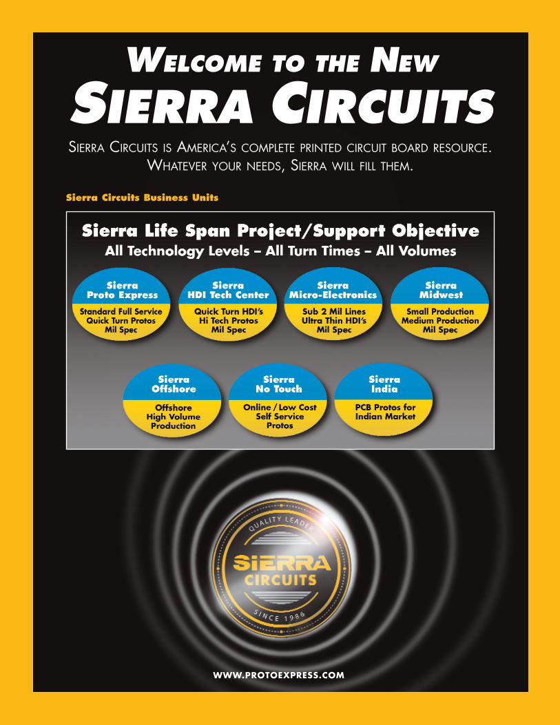
WELCOME TO THE NEW
SIERRA CIRCUITSSIERRA CIRCUITS IS AMERICA’S COMPLETE PRINTED CIRCUIT BOARD RESOURCE.
WHATEVER YOUR NEEDS, SIERRA WILL FILL THEM.
Sierra Circuits Business Units
WWW.PROTOEXPRESS.COM
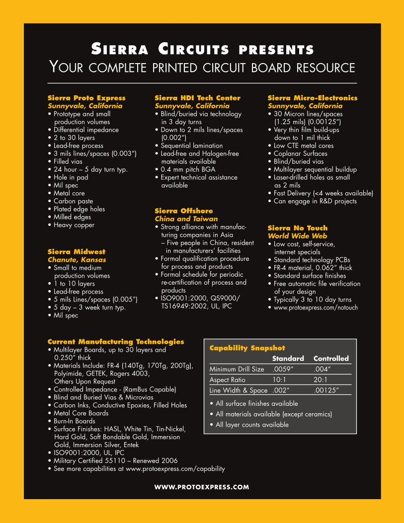
SIERRA CIRCUITS PRESENTSYOUR COMPLETE PRINTED CIRCUIT BOARD RESOURCE
Sierra Proto ExpressSunnyvale, California• Prototype and small
production volumes • Differential impedance• 2 to 30 layers• Lead-free process• 3 mils lines/spaces (0.003”)• Filled vias• 24 hour – 5 day turn typ. • Hole in pad• Mil spec• Metal core• Carbon paste• Plated edge holes• Milled edges• Heavy copper
Sierra HDI Tech CenterSunnyvale, California• Blind/buried via technology
in 3 day turns • Down to 2 mils lines/spaces
(0.002”)• Sequential lamination• Lead-free and Halogen-free
materials available• 0.4 mm pitch BGA• Expert technical assistance
available
Sierra MidwestChanute, Kansas• Small to medium
production volumes • 1 to 10 layers• Lead-free process• 5 mils Lines/spaces (0.005”)• 5 day – 3 week turn typ.• Mil spec
Sierra Micro-ElectronicsSunnyvale, California• 30 Micron lines/spaces
(1.25 mils) (0.00125”)• Very thin film build-ups
down to 1 mil thick• Low CTE metal cores• Coplanar Surfaces• Blind/buried vias• Multilayer sequential buildup• Laser-drilled holes as small
as 2 mils• Fast Delivery (<4 weeks available)• Can engage in R&D projects
Sierra OffshoreChina and Taiwan• Strong alliance with manufac-
turing companies in Asia– Five people in China, resident
in manufacturers’ facilities• Formal qualification procedure
for process and products• Formal schedule for periodic
re-certification of process and products
• ISO9001:2000, QS9000/ TS16949:2002, UL, IPC
Sierra No TouchWorld Wide Web• Low cost, self-service,
internet specials• Standard technology PCBs• FR-4 material, 0.062” thick• Standard surface finishes• Free automatic file verification
of your design• Typically 3 to 10 day turns• www.protoexpress.com/notouch
Current Manufacturing Technologies• Multilayer Boards, up to 30 layers and
0.250” thick• Materials Include: FR-4 (140Tg, 170Tg, 200Tg),
Polyimide, GETEK, Rogers 4003, Others Upon Request
• Controlled Impedance - (RamBus Capable)• Blind and Buried Vias & Microvias• Carbon Inks, Conductive Epoxies, Filled Holes• Metal Core Boards• Burn-In Boards• Surface Finishes: HASL, White Tin, Tin-Nickel,
Hard Gold, Soft Bondable Gold, Immersion Gold, Immersion Silver, Entek
• ISO9001:2000, UL, IPC• Military Certified 55110 – Renewed 2006• See more capabilities at www.protoexpress.com/capability
Capability Snapshot
Standard ControlledMinimum Drill Size .0059” .004”Aspect Ratio 10:1 20:1Line Width & Space .002” .00125”
• All surface finishes available• All materials available (except ceramics)• All layer counts available
WWW.PROTOEXPRESS.COM
SIERRA CIRCUITS800.763.7503
1108 WEST EVELYN AVENUE, SUNNYVALE, CA 94086, USAWWW.PROTOEXPRESS.COM
STICK AROUND, THERE’S A LOT MORE TO COME: MORE ACQUISITIONS, HIGHER TECHNOLOGY, RESEARCH AND
DEVELOPMENT THAT IS GOING TO CHANGE EVERYTHING!
WE HAVE SERVED INNOVATORS EVERYWHERE SINCE 1986.ASK US WHAT WE CAN DO FOR YOU!
AND WE’REJUST GETTING
STARTED...
TO REQUEST A QUOTE
UPLOAD FILES ONLINE AT
www.protoexpress.com/customquoteOR
EMAIL FILES TO: [email protected]