Shape-Controlled Micro/Nanostructures of 9,10 ...
4
Published: March 31, 2011 r2011 American Chemical Society 7924 dx.doi.org/10.1021/jp112195k | J. Phys. Chem. C 2011, 115, 7924–7927 ARTICLE pubs.acs.org/JPCC Shape-Controlled Micro/Nanostructures of 9,10-Diphenylanthracene (DPA) and Their Application in Light-Emitting Devices Bo Yang, †,‡ Jinchong Xiao, †,‡ Jen It Wong, § Jun Guo, ‡ Yuechao Wu, ‡ Lijin Ong, ‡ Luciana Lisa Lao, ‡ Freddy Boey, ‡ Hua Zhang, ‡ Hui Ying Yang,* ,§ and Qichun Zhang* ,‡ † Colleage of Chemistry and Environmental Science, Hebei University, Baoding 071002, P. R. China ‡ School of Materials Science and Engineering, Nanyang Technological University, 50 Nanyang Avenue, Singapore 639798 (Singapore) § Pillar of Engineering Product Development, Singapore University of Technology and Design, 287 Ghim Moh Road, Singapore 279623 b S Supporting Information 1. INTRODUCTION The assembly of organic small molecules into micro/nanos- tructures, whose properties are beyond those of their bulk compo- nents, have attracted extensive attention not only in fundamental science but also in potential technological applications. 16 Many reports have demonstrated that the properties of these micro/ nanostructures can be easily tailored by molecular design, chemical modification of their structures, doping treatment, or chemical conversion. Especially, the shape control, size management, and surface modification of organic micro/nanostructures have provided a powerful platform to tune their optical and electronic properties. 7 Because 9,10-diphenylanthrance (DPA, Scheme 1) is a highly fluorescent molecule and has been widely used in organic optoelec- tronics, the investigation of the shape-dependent properties of DPA micro/nanostructures might be helpful in enhancing the devices’ performance and in preparing other polycyclic aromatic micro/ nanomaterials, whose structures are similar to DPA molecules. Recently, Lee et al. have reported that DPA molecules readily self- assembled into nanoribbons and nanorods by varying the solubility of DPA molecules in the preparation solution. 3a To achieve a detailed understanding of the shape-dependent property of DPA micro/nanostructures and explore the relationship between shape and the performance of organic light-emitting diodes (OLED), we reinvestigated the DPA system and obtained two new shapes of DPA micro/nanostructures: octahedron and sphere. In addition, the performance of OLEDs based on various shapes of DPA micro/ nanostructures such as octahedron, microrod, nanowire, and nano- spheres has been tested and compared in this work. Our results show that the different shapes of DPA micro/nanostructures do affect the performance of diodes and the nanowire is the best shape for heterojunction light emitting diode (LED) devices. 2. EXPERIMENTAL SECTION Materials. 9,10-Diphenylanthracene (DPA) and tetrahydrofur- an (THF) were purchased from Alfa Aesar company (Germany) Scheme 1. Structure of 9,10-Diphenylanthracene Received: December 22, 2010 Revised: March 10, 2011 ABSTRACT: Two novel shapes of 9,10-diphenylanthracene (DPA) micro/nanostructures: octahedron and sphere together with microrod and nanowire have been synthesized via a surfac- tant-assisted self-assembling process. These micro/nanostruc- tures have been characterized by UVvis, fluorescence spectra, X-ray diffraction (XRD), field emission scanning electron micro- scope (FESEM), and transmission electron microscope (TEM). Our results indicated that the absorption and emission spectra of as-prepared particles were slightly blue-shift when the shape of DPA particles changed from octahedron to microrod and finally to nanowire. This result could be explained by the different growth directions of DPA micro/nanostructures. To study the relationship between shape and devices’ performance, the heterojunction light emitting diode (LED) devices of quartz/ITO/ organic particles/n-SiC/Ti(10 nm)/Au(120 nm) have been prepared. The testing results showed that the different shapes of DPA micro/nanostructures did affect the performance of diodes and the nanowire was the best shape for the heterojunction light emitting diode (LED) devices.
Transcript of Shape-Controlled Micro/Nanostructures of 9,10 ...
Published: March 31, 2011
r 2011 American Chemical Society 7924 dx.doi.org/10.1021/jp112195k | J. Phys. Chem. C 2011, 115, 7924–7927
ARTICLE
pubs.acs.org/JPCC
Shape-Controlled Micro/Nanostructures of 9,10-Diphenylanthracene(DPA) and Their Application in Light-Emitting DevicesBo Yang,†,‡ Jinchong Xiao,†,‡ Jen It Wong,§ Jun Guo,‡ Yuechao Wu,‡ Lijin Ong,‡ Luciana Lisa Lao,‡
Freddy Boey,‡ Hua Zhang,‡ Hui Ying Yang,*,§ and Qichun Zhang*,‡
†Colleage of Chemistry and Environmental Science, Hebei University, Baoding 071002, P. R. China‡School of Materials Science and Engineering, Nanyang Technological University, 50 Nanyang Avenue, Singapore 639798 (Singapore)§Pillar of Engineering Product Development, Singapore University of Technology and Design, 287 Ghim Moh Road,Singapore 279623
bS Supporting Information
1. INTRODUCTION
The assembly of organic small molecules into micro/nanos-tructures, whose properties are beyond those of their bulk compo-nents, have attracted extensive attention not only in fundamentalscience but also in potential technological applications.1�6 Manyreports have demonstrated that the properties of these micro/nanostructures can be easily tailored by molecular design, chemicalmodification of their structures, doping treatment, or chemicalconversion. Especially, the shape control, size management, andsurfacemodificationof organicmicro/nanostructures have provideda powerful platform to tune their optical and electronic properties.7
Because 9,10-diphenylanthrance (DPA, Scheme 1) is a highlyfluorescent molecule and has been widely used in organic optoelec-tronics, the investigation of the shape-dependent properties of DPAmicro/nanostructures might be helpful in enhancing the devices’performance and in preparing other polycyclic aromatic micro/nanomaterials, whose structures are similar to DPA molecules.Recently, Lee et al. have reported that DPA molecules readily self-assembled into nanoribbons and nanorods by varying the solubilityof DPA molecules in the preparation solution.3a To achieve adetailed understanding of the shape-dependent property of DPAmicro/nanostructures and explore the relationship between shapeand the performance of organic light-emitting diodes (OLED), wereinvestigated the DPA system and obtained two new shapes of
DPA micro/nanostructures: octahedron and sphere. In addition,the performance of OLEDs based on various shapes of DPAmicro/nanostructures such as octahedron, microrod, nanowire, and nano-spheres has been tested and compared in this work. Our resultsshow that the different shapes of DPA micro/nanostructures doaffect the performance of diodes and the nanowire is the best shapefor heterojunction light emitting diode (LED) devices.
2. EXPERIMENTAL SECTION
Materials. 9,10-Diphenylanthracene (DPA) and tetrahydrofur-an (THF) were purchased from Alfa Aesar company (Germany)
Scheme 1. Structure of 9,10-Diphenylanthracene
Received: December 22, 2010Revised: March 10, 2011
ABSTRACT: Two novel shapes of 9,10-diphenylanthracene(DPA) micro/nanostructures: octahedron and sphere togetherwith microrod and nanowire have been synthesized via a surfac-tant-assisted self-assembling process. These micro/nanostruc-tures have been characterized by UV�vis, fluorescence spectra,X-ray diffraction (XRD), field emission scanning electron micro-scope (FESEM), and transmission electron microscope (TEM).Our results indicated that the absorption and emission spectra ofas-prepared particles were slightly blue-shift when the shape ofDPA particles changed from octahedron to microrod and finallyto nanowire. This result could be explained by the different growth directions of DPA micro/nanostructures. To study therelationship between shape and devices’ performance, the heterojunction light emitting diode (LED) devices of quartz/ITO/organic particles/n-SiC/Ti(10 nm)/Au(120 nm) have been prepared. The testing results showed that the different shapes of DPAmicro/nanostructures did affect the performance of diodes and the nanowire was the best shape for the heterojunction light emittingdiode (LED) devices.
7925 dx.doi.org/10.1021/jp112195k |J. Phys. Chem. C 2011, 115, 7924–7927
The Journal of Physical Chemistry C ARTICLE
and VWR Singapore PTE Ltd. (France), respectively. Poly-(ethylene glycol)-block-poly(propyleneglycol)-block-poly-(ethylene glycol) (P123), cetyltrimethylammonium bromide(CTAB), sodium dodecyl sulfate (SDS), and polyvinylpyrroli-done (PVP40T, wt 40 000) were purchased from Aldrich Com-pany (Germany). All chemicals were used directly without furtherpurification. Ultrapure water was obtained from the Millipore S.A. 67120 apparatus (France) with a resistivity of 18.2 MΩ cm.Methods. The octahedral DPA microcrystals were prepared
by adding 1 mL of 0.5 mM DPA/THF solution into 5 mL watercontaining P123 (1 mg/mL) with a strong stirring. After stirringfor 5 min, the solution was kept undisturbed overnight at roomtemperature before characterization. If the surfactant P123 wasreplaced by CTAB and SDA and other conditions kept same,nanowires rather than octahedrons were produced.DPA microrods: 0.5 mL of 1 mM DPA/THF solution was
diluted by 0.25 mL THF and was then injected into 5.25 mLP123 (1 mg/mL) aqueous solution. After stirring for 5 min, theobtained solution was aged overnight to give DPA microrods.DPA nanowires: 0.5 mL of 1 mMDPA/THF solution was added
to 5.5 mL P123 aqueous solution with strong stirring for 5 min. Theas-prepared solution was left standing overnight before purification.DPA nanospheres: 0.5 mL of 1 mM DPA/THF solution was
injected into 5.5 mL PVP (0.5 mg/mL) aqueous solution. Afterstirring for 5 min, the obtained solution was aged overnight toform DPA nanospheres.The preparation of SEM samples: A drop (30μL) of the solution
was put on a silica wafer and dried over 12 h. The as-preparedsamples were then coated with platinum in an ion coater for 40 s.Characterization. The sizes and shapes of the micro/nanos-
tructures were observed on a FESEM (JSM-6340F, JEOL) at anaccelerating voltage of 5 kV. The samples were also studied byTEM (JEM 2010F) to further confirm their morphologies. TheX-ray diffraction (XRD) patterns were performed on a Bruker D8X-ray diffractometer with Cu KR radiation. The operating 2θ angleranges from 5 to 90�. The cell data were obtained using a JADEsoftware to simulate XRD patterns. The UV�vis absorption andfluorescence spectra of DPA nanostructures were recorded onShimadzu UV-2501 and RF-5301 spectrophotometer, respectively.The FTIR spectra (KBr pellets) were performed on PerkinElmerspectrum GX.
Fabrication and Testing of Devices. The heterojunctionLED was fabricated according to our previous procedure.8
Briefly, on a clean n-SiC substrate, a Ti/Au contact (size ofabout 2 � 2 mm2, ∼10 nm thick for Ti, and ∼120 nm thick forAu) was deposited by using electron beam evaporation at roomtemperature. Various DPA micro/nanostructures were drop-coated on the other side of n-SiC substrate. The top of theorganic layers was covered by the ITO electrode, which was usedas DPA micro/nanostructures’ contact. The spectra were mea-sured by connecting the cathode and anode of a constant voltagesource to the ITO and Ti(10 nm)/Au(120 nm) metal contacts,respectively. Light was collected from the surface of the ITO glassby an optical fiber.
3. RESULTS AND DISCUSSION
Figure 1 shows the typical SEM images of the DPA nano/microstructures with different morphologies, which were preparedby the surfactant-assisted precipitation method via changing theratio of DPA, water, surfactants, and organic solvents. As shown inpart a of Figure 1, repeatablemicrooctahedronswere observedwhen1 mL 0.5 mM DPA/THF solution was dropped into 5 mL P123water solution (the ratio of THF/P123 is 1:5) with a strong stirring.The average size of as-prepared microoctahedrons is about 700 nm.When the ratio of THF/P123 increased to 1:7, microrods with thediameter in the range of 500�600 nm and the length between 1 and2 μmwere formed after 12 h (part b of Figure 1). When the ratio ofTHF/P123 was further increased into 1:11, the nanowires(diameter: 100�300 nm and length 2�4 μm) were obtained(part c of Figure 1). The insert in part c of Figure 1 shows a typicalnanowire with the smooth and clean surface. In addition, the otherratios of THF and P123 solution were also performed. When theratio is less than 1:5, the irregular structures including microoctahe-drons and rods were formed, while the ratio is larger than 1:11, onlythe nanowires can be observed (Figure S1 of the SupportingInformation). It is very clear that the ratio of THF/P123 doeschange the shape of DPAmicro/nanostructures frommicrooctahe-drons to microrods and then to nanowires.
The effect of surfactants on the aggregation behavior of DPAmolecules was also investigated. When P123 surfactant wasreplaced by PVP, a large quantity of nanospheres with the sizein the range of 100�250 nm were obtained. Unlike P123surfactant, where the shapes changed as a function of the ratios ofTHF/P123, spherical shapes were retained when PVP surfactantwas used at various THF/PVP ratios, ranging from 1:5 to 1:11.Further investigationswith other surfactants such asCTABandSDSonly gave microrods (Figure S2 of the Supporting Information).
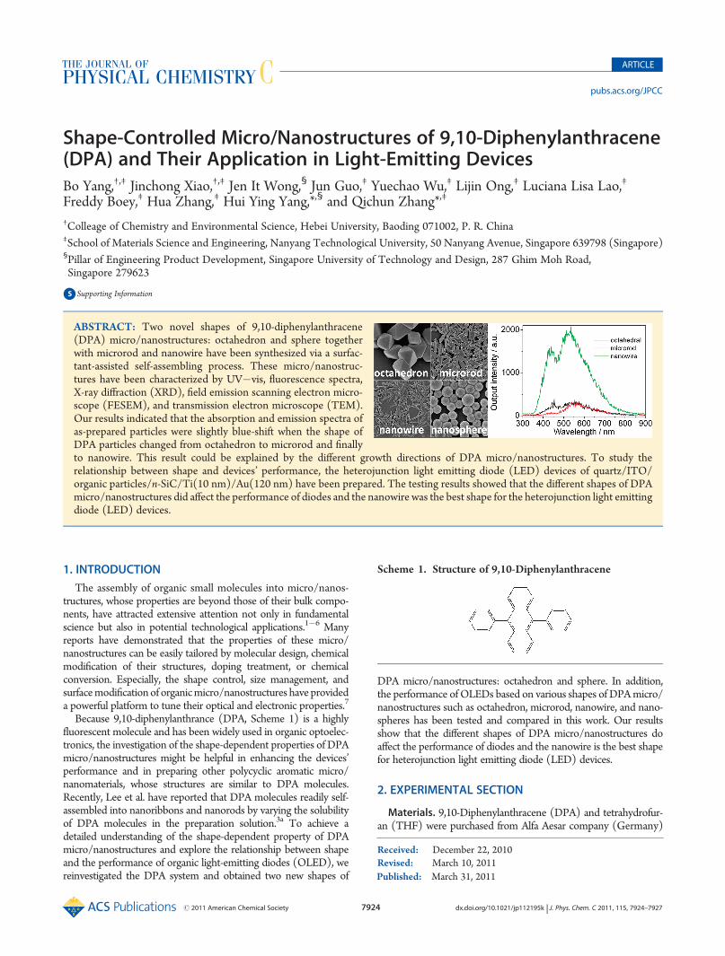
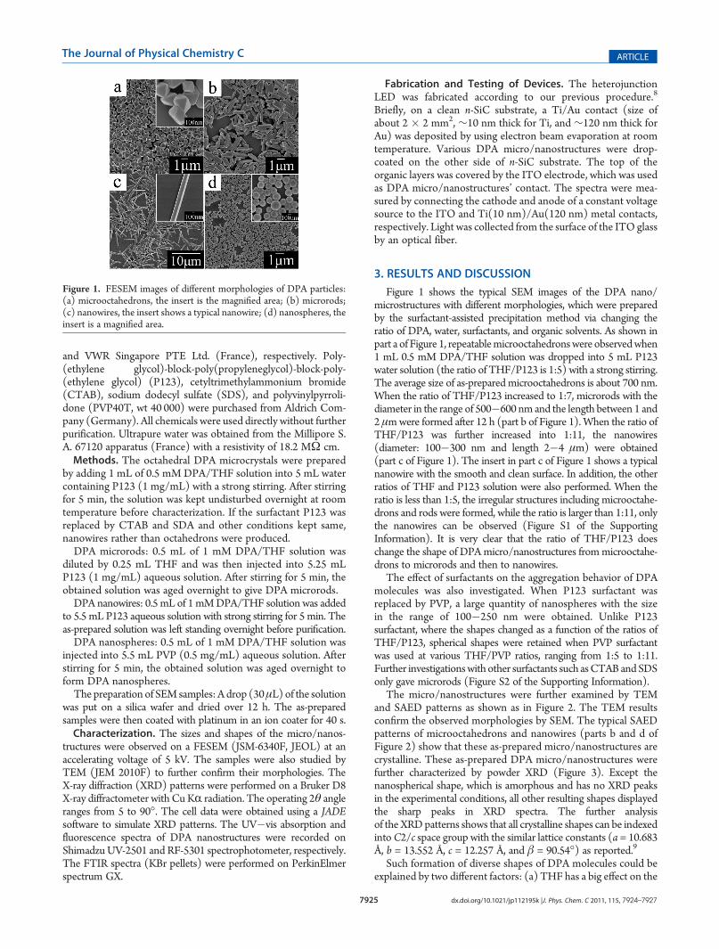
The micro/nanostructures were further examined by TEMand SAED patterns as shown as in Figure 2. The TEM resultsconfirm the observed morphologies by SEM. The typical SAEDpatterns of microoctahedrons and nanowires (parts b and d ofFigure 2) show that these as-prepared micro/nanostructures arecrystalline. These as-prepared DPA micro/nanostructures werefurther characterized by powder XRD (Figure 3). Except thenanospherical shape, which is amorphous and has no XRD peaksin the experimental conditions, all other resulting shapes displayedthe sharp peaks in XRD spectra. The further analysisof the XRDpatterns shows that all crystalline shapes can be indexedintoC2/c space group with the similar lattice constants (a = 10.683Å, b = 13.552 Å, c = 12.257 Å, and β = 90.54�) as reported.9
Such formation of diverse shapes of DPA molecules could beexplained by two different factors: (a) THF has a big effect on the
Figure 1. FESEM images of different morphologies of DPA particles:(a) microoctahedrons, the insert is the magnified area; (b) microrods;(c) nanowires, the insert shows a typical nanowire; (d) nanospheres, theinsert is a magnified area.
7926 dx.doi.org/10.1021/jp112195k |J. Phys. Chem. C 2011, 115, 7924–7927
The Journal of Physical Chemistry C ARTICLE
solubility of DPA molecules, which is a very important factorduring the dynamic growth (size, direction, and shape) of DPAparticles,3a and (b) the interaction between surfactants and DPAmolecules plays another key role during the growth of DPAparticles. The surfactants such as P123, CTAB, and SDS have aweak dipolar�dipolar interaction with DPA molecules, whichhas less effect on the self-assembly of DPA molecules. In theseconditions, DPA molecules can form crystalline structures moreeasily. However, the self-aggregation might be disturbed andamorphous particles are formed if the surfactant (e.g., PVP) has astrong interaction (π 3 3 3π attractions) with DPA molecules.Currently, the behavior of surfactants is still in debate.
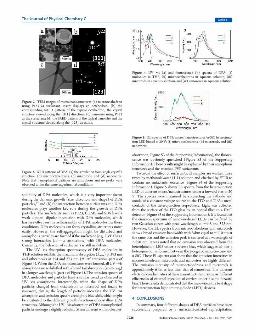
The UV�vis absorption spectroscopy of DPA molecules inTHF solution exhibits the maximum absorption (λmax) at 393 nmand other peaks at 354 and 373 nm (π�π* transition, part a ofFigure 4).When the DPA nanostructures were formed, all UV�visabsorptions are red-shifted with a broad tail absorption (scattering)in a longer wavelength (part a of Figure 4). The emission spectra ofDPA molecules and particles have a similar trend as observed inUV�vis absorptions. Interestingly, when the shape of DPAparticles changed from octahedron to microrod and finally tonanowire, that is, the length of particles increases, the UV�visabsorption and emission spectra are slightly blue-shift, whichmightbe attributed to the different growth directions of crystalline DPAstructures. Although the UV�vis absorption of DPA nanosphericalparticles undergo a slightly red-shift (6 nmdifferentwithmolecules’
absorption, Figure S3 of the Supporting Information), the fluores-cence was obviously quenched (Figure S3 of the SupportingInformation). These resultsmight be explained by their amorphousstructures and the attached PVP surfactants.
To avoid the effect of surfactants, all samples are washed threetimes by methanol/water (1:1) solution and checked by FTIR toconfirm no surfactants’ existence (Figure S4 of the SupportingInformation). Figure 5 shows EL spectra from the heterojunctionLED of different micro/nanostructures under a forward bias of 20V. The spectra were measured by connecting the cathode andanode of a constant voltage source to the ITO and Ti/Au metalcontacts of the heterojunction respectively. Light was collectedfrom the surface of the ITO glass by an optical fiber to a PMTdetector (Figure S5 of the Supporting Information). It is found thatthe emission spectrum of nanowire-based LEDs can be fitted bytwo Gaussian curves with peak wavelength at ∼445 and 525 nm.However, the EL spectra from microoctahedrons and microrodsshow a broad emission bandwidth with fwhm equal to∼110 nm atthe same bias and the emission peak is centered at a wavelength of∼550 nm. It was noted that no emission was observed from theheterojunction LED under a reverse bias, which suggested that aheterojunction is formed between the p-organic nanostructure andn-SiC. These EL spectra also show that the emission intensities inmicrooctahedrons, microrods, and nanowires are highly different.The emission intensity of microoctahedrons and microrods isapproximately 6 times less than that of nanowires. The differentelectrical conductivities of these nanostructures may cause differentefficiencies of external injection of carriers under a same forwardbias. These results demonstrated that the nanowire is the best shapefor heterojunction light emitting diode (LED) devices.
4. CONCLUSIONS
In summary, four different shapes of DPA particles have beensuccessfully prepared by a surfactant-assisted reprecipitation
Figure 5. EL spectra of DPA micro/nanostructures/n-SiC heterojunc-tion LED biased at 20 V: (i) microoctahedrons, (ii) microrods, and (iii)nanowires.
Figure 2. TEM images of micro/nanostructures (a) microoctahedronusing P123 as surfactant, insert displays an octahedron; (b) thecorresponding SAED pattern of the typical octahedron, the crystalstructure viewed along the [311] direction; (c) nanowire using P123as the surfactant; (d) the SAED pattern of the typical nanowire and thecrystal structure viewed along the [123] direction.
Figure 3. XRD patterns of DPA: (a) the simulation from single crystal’sstructure, (b) microoctahedrons, (c) microrods, and (d) nanowires.Note that nanospherical particles are amorphous and no peaks wereobserved under the same experimental conditions.
Figure 4. UV�vis (a) and fluorescence (b) spectra of DPA: (i)molecules in THF, (ii) microoctahedrons in aqueous solution, (iii)microrods in aqueous solution, and (iv) nanowires in aqueous solution.

7927 dx.doi.org/10.1021/jp112195k |J. Phys. Chem. C 2011, 115, 7924–7927
The Journal of Physical Chemistry C ARTICLE
method. The as-prepared shapes show different UV�vis absorp-tions and emissions phenomena. Further study about the effectof different shapes on OLED application indicates that thenanowire is the best shape that gives the best performance forsuch devices.
’ASSOCIATED CONTENT
bS Supporting Information. SEM images of DPA particlesprepared from THF/P123 (THF/P123 = 1:3 and 1:15) watersolution; SEM images of DPA prepared from different surfac-tants; UV�vis absorption and fluorescence spectra of DPAnanospheres; FTIR spectra of different shapes of DPA particlesafter washing; and the lighting images of different shapes of DPAparticles on OLED. This material is available free of charge viathe Internet at http://pubs.acs.org.
’AUTHOR INFORMATION
Corresponding Author*Tel:þ65-67904705, fax:þ65-67909081, e-mail: [email protected] (Q.Z.); [email protected] (H.Y.).
’ACKNOWLEDGMENT
Q.Z. acknowledges financial support from Nanyang Techno-logical University (start-up grant) and the AcRF Tier 1 (RG 18/09) fromMOE. H. Y. acknowledges support from the Singapore-MIT International Design Centre research fund.
’REFERENCES
(1) (a) Henze, O.; Feast, W. J.; Gardebien, F.; Jonkheijm, P.;Lazzaroni, R.; Lecl�ere, P.; Meijer, E. W.; Schenning, A. P. H. J. J. Am.Chem. Soc. 2006, 128, 5923. (b) Hoeben, F. J. M.; Jonkheijm, P.; Meijer,E. W.; Schenning, A. P. H. J. Chem. Rev. 2005, 105, 1491. (c) Feyter,S. D.; Miura, A.; Yao, S.; Chen, Z.; W€urthner, F.; Jonkhejm, P.;Schenning, A. P. H. J.; Meijer, E. W.; Schryver, F. C. D. Nano Lett.2005, 5, 77. (d) Schenning, A. P. H. J.; Meijer, E. W. Chem. Commun.2005, 3245.(2) (a) Liu, H.; Xiu, J.; Li, Y.; Li, Y. Acc. Chem. Res. 2010, 43, 1496.
(b) Xu, J.; Zheng, H.; Liu, H.; Zhou, C.; Zhao, Y.; Li, Y.; Li, Y. J. Phys.Chem. C 2010, 114, 2925. (c) Huang, C.; Li, Y.; Yang, J.; Cheng, N.; Liu,H.; Li, Y. Chem. Commun. 2010, 3161. (d) Huang, C.; Wen, L.; Liu, H.;Li, Y.; Liu, X.; Yuan, M.; Zhai, J.; Jiang, L.; Zhu, D. Adv. Mater. 2009,21, 1721. (e) Xiao, J.; Xu, J.; Cui, S.; Liu, H.; Wang, S.; Li, Y. Org. Lett.2008, 10, 645. (f) Guo, Y.; Tang, Q.; Liu, H.; Zhang, Y.; Li, Y.; Hu, W.;Wang, S.; Zhu, D. J. Am. Chem. Soc. 2008, 130, 9198.(3) (a) Zhang, X.; Yuan, G.; Li, Q.; Wang, B.; Zhang, X.; Zhang, R.;
Chang, J. C.; Lee, C. S.; Lee, S. T. Chem. Mater. 2008, 20, 6945. (b)Zhang, X.; Zhang, X.; Wang, B.; Zhang, C.; Chang, J. C.; Lee, C. S.; Lee,S. T. J. Phys. Chem. C. 2008, 112, 16264. (c) Zhang, X.; Zhang, X.; Zou,K.; Lee, C. S.; Lee, S. T. J. Am. Chem. Soc. 2007, 129, 3527. (d) Zhang, X.;Dong, C.; Zapien, J. A.; Ismathullakhan, S.; Kang, Z.; Jie, J.; Zhang, X.;Chang, J. C.; Lee, C. S.; Lee, S. T. Angew. Chem., Int. Ed. 2009, 48, 9121.(4) (a) Li, R.; Hu, W.; Liu, Y.; Zhu, D. Acc. Chem. Res. 2010, 43, 529.
(b) Dong, H.; Jiang, S.; Jiang, L.; Liu, Y.; Li, H.; Hu, W.; Wang, E.; Yan,S.; Wei, Z.; Xu, W.; Gong, X. J. Am. Chem. Soc. 2009, 131, 17315. (c)Wang, C.; Liu, Y.; Ji, Z.; Wang, E.; Li, R.; Jiang, H.; Tang, Q.; Li, H.; Hu,W. Chem. Mater. 2009, 21, 2840. (d) Xiao, K.; Li, R.; Tao, J.; Payzant,E. A.; Ivanov, I. N.; Puretzky, A. A.; Hu, W.; Geohegan, D. B. Adv. Funct.Mater. 2009, 19, 3776. (e) Jiang, L.; Hu, W.; Wei, Z.; Xu, W.; Meng, H.Adv. Mater. 2009, 21, 3649.(5) (a) Lee, H. S.; Kwak, D.; Lee, W. H.; Cho, J. H.; Cho, K. J. Phys.
Chem. C 2010, 114, 2329. (b) Kim, D. H.; Lee, D. Y.; Lee, H. S.; Lee,W. H.; Kim, Y. H.; Han, J. I.; Cho, K. Adv. Mater. 2007, 19, 678.
(6) (a) Kim, H. J.; Kang, S. K.; Lee, Y. K.; Seok, C.; Lee, J. K.; Zin,W. C.; Lee, M. Angew. Chem., Int. Ed. 2010, 49, 8471. (b) Kim, J. K.; Lee,E.; Kim, M. C.; Sim, E.; Lee, M. J. Am. Chem. Soc. 2009, 131, 17768. (c)Lim, Y. B.; Moon, K. S.; Lee, M. J. Mater. Chem. 2008, 18, 2909. (d) Ryu,J. H.; Kim, H. J.; Huang, Z.; Lee, E.; Lee, M. Angew. Chem., Int. Ed. 2006,45, 5304.
(7) (a) Xiao, J.; Kusuma, D. Y.; Wu, Y.; Boey, F.; Zhang, H.; Lee,P. S.; Zhang, Q. Chem Asian J. 2011, 6, 801. (b) Xiao, J.; Yin, Z.; Li, H.;Zhang, Q.; Boey, F.; Zhang, H.; Zhang, Q. J. Am. Chem. Soc. 2010,132, 6926. (c) Zhao, Y. S.; Fu, H.; Peng, A.; Ma, Y.; Liao, Q.; Yao, J. Acc.Chem. Res. 2010, 43, 409. (d) McGrath, K. K.; Jang, K.; Robins, K. A.;Lee, D. C. Chem.—Eur. J. 2009, 15, 4070. (e) Huang, J.; Fu, H.; Wu, Y.;Chen, S.; Shen, F.; Zhao, X.; Liu, Y.; Yao, J. J. Phys. Chem. C 2008,112, 2689. (f) Briseno, A. L.; Mannsfeld, S. C. B.; Jenekhe, S. A.; Bao,Z. N.; Xia, Y. N.Mater. Today 2008, 11, 38. (g) Jiang, L.; Fu, Y.; Li, H.;Hu, W. J. Am. Chem. Soc. 2008, 130, 3937. (l) Lee, D. C.; Jang, K.;McGrath, K. K.; Uy, R.; Robins, K. A.; Hatchett, D. W. Chem. Mater.2008, 20, 3688. (h) Niu, Q.; Zhou, Y.; Wang, L.; Peng, J.; Wang, J.; Pei,J.; Cao, Y.Adv.Mater. 2008, 20, 964. (i) Laschat, S.; Baro, A.; Steinke, N.;Giesselmann, F.; H€agele, C.; Scalia, G.; Judele, R.; Kapatsina, E.; Sauer,S.; Schreivogel, A.; Tosoni, M. Angew. Chem., Int. Ed. 2007, 46, 4832. (j)Ajayaghosh, A.; Praveen, V. K. Acc. Chem. Res. 2007, 40, 644. (k) Hill,J. P.; Jin, W.; Kosaka, A.; Fukushima, T.; Ichihara, H.; Shimomura, T.;Ito, K.; Hashizume, T.; Ishii, N.; Aida, T. Science 2004, 304, 1481.
(8) Xiao, J.; Yang, H.; Yin, Z.; Guo, J.; Boey, F.; Zhang, H.; Zhang, Q.J. Mater. Chem. 2011, 21, 1423.
(9) Langer, V.; Becker, H. D. Z. Kristallogr. 1992, 199, 313.(10) (a) MaRae, E. G.; Kasha, M. Physical Processes in Radiation
Biology; Augenstein, Rosen-berg Mason, Ed.; Academic Press: NewYork, 1964. (b) Beckers, E. H. A.;Meskers, S. C. J.; Schenning, A. P. H. J.;Chen, Z. J.; W€urthner, F.; Marsal, P.; Beljonne, D.; Cornil, J.; Janssen,R. A. J. J. Am. Chem. Soc. 2006, 128, 649. (c) Xiao, J.; Li, Y.; Song, Y.;Jiang, L.; Li, Y.; Wang, S.; Liu, H.; Xu, W.; Zhu, D. Tetrahedron Lett.2007, 48, 7599.


![Metal Oxide Thin Films and Nanostructures Made by ALD · mands is atomic layer deposition (ALD)[9,10]. ALD, also known as atomic layer epitaxy (ALE) or atomic layer chemical vapour](https://static.fdocuments.net/doc/165x107/60af0a63ec0db37505778719/metal-oxide-thin-films-and-nanostructures-made-by-ald-mands-is-atomic-layer-deposition.jpg)