
Resistive RAM ( Resistive RAM (ReRAM) Technology ) Technology ...

SHA-3 Implementation Using ReRAM basedIn-Memory Computing Architecture
Debjyoti Bhattacharjee, Vikram Kumar Pudi and Anupam
Chattopadhyay
School of Computer Science and Engineering
Nanyang Technological University,
Singapore
Email : {debjyoti001, pudi, anupam}@ntu.edu.sg

Outline
• Background and Motivation
• SHA-3 basics
• Proposed Mapping of SHA-3
• Experimental Results
• Conclusion
Background and Motivation
• Leon Chua’s missing memristor was found in 20081
• ReRAM is gaining prominence due to:
– High storage density
– Low leakage power
– Ability to perform functionally complete set of Boolean operations.
• Multiple arithmetic circuits have been proposed using memristors2
• Neuromorphic Computing has also been demonstrated feasible3
• General purpose computing architectures have been proposed using in-
memory capabilities of Resistive RAM (ReRAM) 4,5
• Level-1 and Level 2 Binary BLAS has been proposed using ReRAMs.6,7
– Estimated throughput is 10x more than GPU based implementations
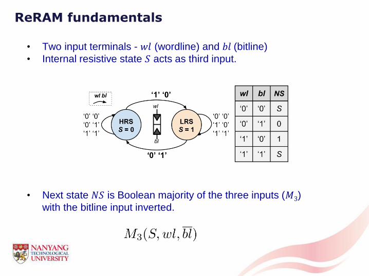
ReRAM fundamentals
• Two input terminals - 𝑤𝑙 (wordline) and 𝑏𝑙 (bitline)
• Internal resistive state 𝑆 acts as third input.
• Next state 𝑁𝑆 is Boolean majority of the three inputs (𝑀3)
with the bitline input inverted.
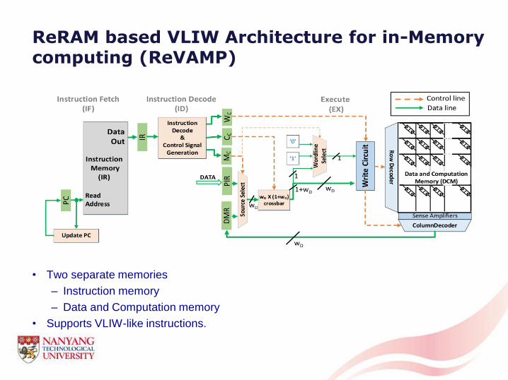
ReRAM based VLIW Architecture for in-Memory computing (ReVAMP)
• Two separate memories
– Instruction memory
– Data and Computation memory
• Supports VLIW-like instructions.
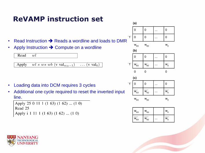
ReVAMP instruction set
• Read Instruction Reads a wordline and loads to DMR
• Apply Instruction Compute on a wordline
• Loading data into DCM requires 3 cycles
• Additional one cycle required to reset the inverted input
line.

Basic Boolean Function realization
• Intrinsic function of ReRAM device
– 𝑀3 𝑆,𝑤𝑙, 𝑏𝑙
• Boolean AND
– a.b = 𝑀3 a, 0, 𝑏
• Boolean OR
– a+b = 𝑀3 a , 1, 𝑏

Outline
• Background and Motivation
• SHA-3 basics
• Proposed Mapping of SHA-3
• Experimental Results
• Conclusion

SHA-3 (Keccak)
• The first cryptographic hash algorithm NIST has developed using a public
competition
• Based on Sponge construction
• For any arbitrary message-length,
– SHA-3 generates a fixed length output (Hash)

SHA-3 Round
• Round function consists of
5-steps
• “A” state matrix
– 5 × 5 matrix
– Each word is 64 bits
– Total state size 1600 bits
• “RC” – Round constant
• Each message operated
upon by 24-Rounds

Outline
• Background and Motivation
• SHA-3 basics
• Proposed Mapping of SHA-3
• Experimental Results
• Conclusion
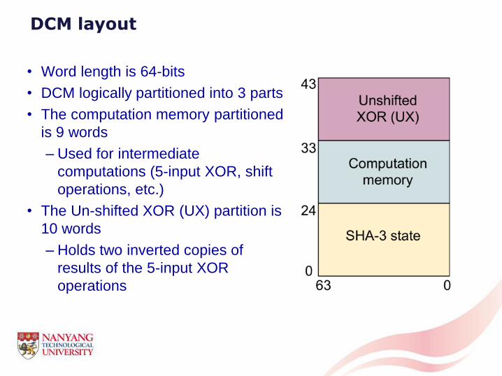
DCM layout
• Word length is 64-bits
• DCM logically partitioned into 3 parts
• The computation memory partitioned
is 9 words
– Used for intermediate
computations (5-input XOR, shift
operations, etc.)
• The Un-shifted XOR (UX) partition is
10 words
– Holds two inverted copies of
results of the 5-input XOR
operations

2-input XOR
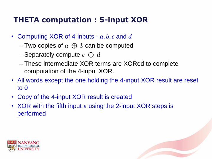
THETA computation : 5-input XOR
• Computing XOR of 4-inputs - 𝑎, 𝑏, 𝑐 and 𝑑
– Two copies of 𝑎 ⊕ 𝑏 can be computed
– Separately compute 𝑐 ⊕ 𝑑
– These intermediate XOR terms are XORed to complete
computation of the 4-input XOR.
• All words except the one holding the 4-input XOR result are reset
to 0
• Copy of the 4-input XOR result is created
• XOR with the fifth input 𝑒 using the 2-input XOR steps is
performed
THETA computation : Fused circular shift with XOR
• Two inverted copies of 5-input XOR is written to UX partition
• Once the previous stage terminates
– Circular Shifted value is written to the Computation memory
partition
• The shifted and non-shifted values are XORed.
• The wordline with intermediate results are RESET.
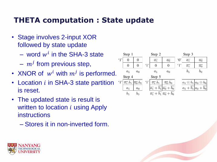
THETA computation : State update
• Stage involves 2-input XOR
followed by state update
– word 𝑤𝑖 in the SHA-3 state
– 𝑚𝑗 from previous step,
• XNOR of 𝑤𝑖 with 𝑚𝑗 is performed.
• Location 𝑖 in SHA-3 state partition
is reset.
• The updated state is result is
written to location 𝑖 using Apply
instructions
– Stores it in non-inverted form.

RHO with PI
• The word 𝑤𝑖 is read out
• the RHO output is written to the Computation memory partition.
• RHO output of 𝑤𝑗 is written to another location in Computation memory
partition.
– location 𝑗 is the new location of word 𝑖
• Word 𝑗 in SHA-3 state is RESET.
• 𝑘𝑖 is written to location 𝑗 in SHA-3 state.
• Location in Computation memory holding 𝑘𝑖 is RESET.
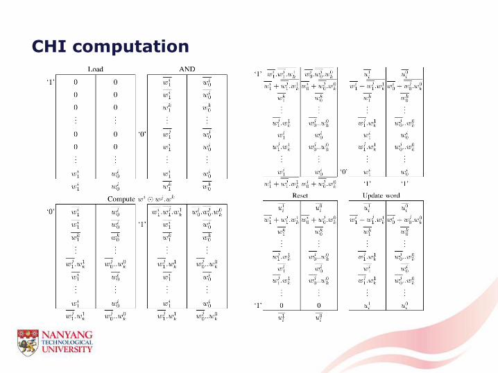
CHI computation
IOTA
• Final step of SHA-3 Round
• Involves computation of XOR with two inputs.
• Requires 12 cycles
– 2 additional cycles needed to reset locations
used for computation.
Outline
• Background and Motivation
• SHA-3 basics
• Proposed Mapping of SHA-3
• Experimental Results
• Conclusion

SHA-3 Latency
• Each ReVAMP instruction (𝑎𝑝𝑝𝑙𝑦, 𝑟𝑒𝑎𝑑) effectively
requires one cycle for execution
– The first instruction requires 3 cycles.
• First Round requires 1261 cycles.
• Next 23 Rounds require 1159 instructions
– Loading State step is not required in these Rounds.
• Overall latency of SHA-3 = 27918 cycles.

SHA-3 Performance Estimate
• Mature ReRAM devices estimated to have 1 𝑛𝑠 access time.
• Effective throughput estimated to be 38.57 Mbps
• Low memory footprint
– DCM 0.33 KB.
– IM 80 KB

Comparison against Existing Designs

Outline
• Background and Motivation
• SHA-3 basics
• Proposed Mapping of SHA-3
• Experimental Results
• Conclusion
Conclusion
• First mapping of SHA-3 on a Logic-in-memory Architecture
• Low memory footprint
• Performance comparable against bit-serial ASIC implementation

Thank You ! Questions?
References
1. Strukov, Dmitri B., Gregory S. Snider, Duncan R. Stewart, and R. Stanley Williams. "The
missing memristor found." nature 453, no. 7191 (2008): 80-83.
2. Siemon, Anne, Stephan Menzel, Rainer Waser, and Eike Linn. "A complementary resistive
switch-based crossbar array adder." IEEE journal on emerging and selected topics in
circuits and systems 5, no. 1 (2015): 64-74.
3. Prezioso, Mirko, Farnood Merrikh-Bayat, B. D. Hoskins, G. C. Adam, Konstantin K.
Likharev, and Dmitri B. Strukov. "Training and operation of an integrated neuromorphic
network based on metal-oxide memristors." Nature 521, no. 7550 (2015): 61-64.
4. Gaillardon, Pierre-Emmanuel, Luca Amar, Anne Siemon, Eike Linn, Rainer Waser, Anupam
Chattopadhyay, and Giovanni De Micheli. "The programmable logic-in-memory (PLiM)
computer." In 2016 Design, Automation & Test in Europe Conference & Exhibition (DATE),
pp. 427-432. IEEE, 2016.
5. Debjyoti Bhattacharjee, Rajeshwari Devadoss and Anupam Chattopadhyay. “ReVAMP :
ReRAM based VLIW Architecture for in-Memory comPuting." In 2017 Design, Automation &
Test in Europe Conference & Exhibition (DATE).
6. D. Bhattacharjee, F. Merchant and A. Chattopadhyay, "Enabling in-memory computation of
binary BLAS using ReRAM crossbar arrays," 2016 IFIP/IEEE International Conference on
Very Large Scale Integration (VLSI-SoC), Tallinn, 2016, pp. 1-6.
7. Debjyoti Bhattacharjee and Anupam Chattopadhyay. Efficient In-Memory computation of
Binary BLAS on ReRAM Crossbar Arrays. In VLSI Design 2017.