
Sequential Circuit Design - Dronacharya
51
Sequential Circuit Design
Transcript of Sequential Circuit Design - Dronacharya
Sequential Circuit Design
Overview
Sequential Circuit Design
Specification
Formulation
State Assignment
Flip-Flop Input and Output Equation
Verification
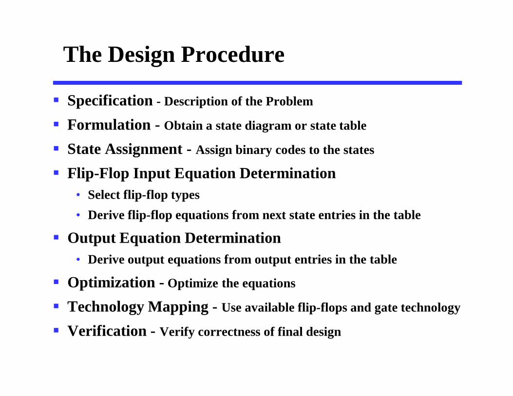
The Design Procedure
Specification - Description of the Problem
Formulation - Obtain a state diagram or state table
State Assignment - Assign binary codes to the states
Flip-Flop Input Equation Determination• Select flip-flop types• Derive flip-flop equations from next state entries in the table
Output Equation Determination• Derive output equations from output entries in the table
Optimization - Optimize the equations
Technology Mapping - Use available flip-flops and gate technology
Verification - Verify correctness of final design
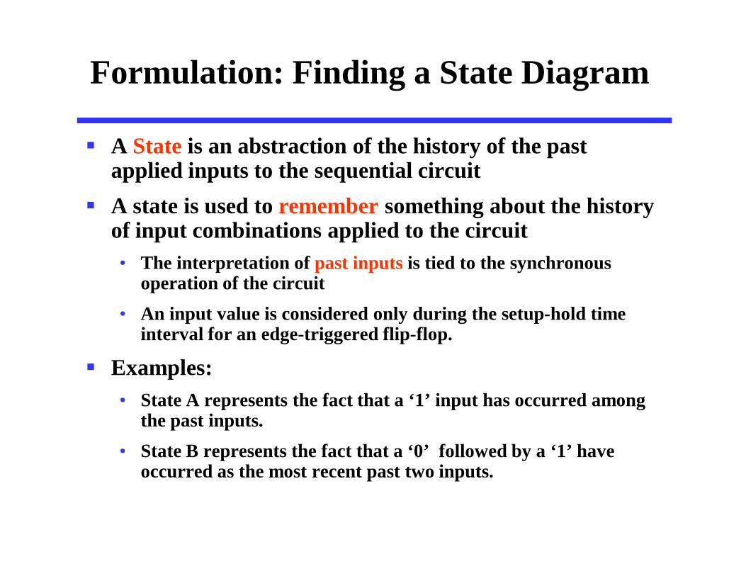
Formulation: Finding a State Diagram
A State is an abstraction of the history of the past applied inputs to the sequential circuit
A state is used to remember something about the history of input combinations applied to the circuit• The interpretation of past inputs is tied to the synchronous
operation of the circuit• An input value is considered only during the setup-hold time
interval for an edge-triggered flip-flop.
Examples:• State A represents the fact that a ‘1’ input has occurred among
the past inputs.• State B represents the fact that a ‘0’ followed by a ‘1’ have
occurred as the most recent past two inputs.
Formulation: Finding a State Diagram
In specifying a circuit, we use states to remember meaningful properties of past input sequences that are essential to predicting future output values
A sequence recognizer is a sequential circuit that produces a distinct output value whenever a prescribed pattern of input symbols occur in sequence, i.e, recognizes an input sequence occurence
We will develop a procedure specific to sequence recognizers to convert a problem statement into a state diagram
Next, the state diagram, will be converted to a state table from which the circuit will be designed
Sequence Recognizer Procedure
Begin in an initial state in which NONE of the initial portion of the sequence has occurred (reset state)
Add a state that recognizes that first symbol has occurred
Add states that recognize each successive symbol
The final state represents the input sequence occurence
Add state transition arcs which specify what happens when a symbol not in the proper sequence has occurred
Add other arcs which transition to states that represent the input subsequence that has occurred• The circuit must recognize the input sequence regardless of
where it occurs within the overall sequence
Sequence Recognizer Example
Example: Recognize the sequence 1101
• Example: the sequence 1111101 contains 1101
Thus, the sequential machine must remember that the first two one's have occurred as it receives another symbol
Also, the sequence 1101101 contains 1101 as both an initial subsequence and a final subsequence with some overlap, i. e., 1101101 or 1101101
The 1 in the middle, 1101101, is in both subsequences
The sequence 1101 must be recognized each time it occurs in the input sequence
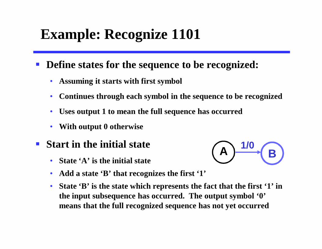
Example: Recognize 1101
Define states for the sequence to be recognized:• Assuming it starts with first symbol
• Continues through each symbol in the sequence to be recognized
• Uses output 1 to mean the full sequence has occurred
• With output 0 otherwise
Start in the initial state• State ‘A’ is the initial state• Add a state ‘B’ that recognizes the first ‘1’• State ‘B’ is the state which represents the fact that the first ‘1’ in
the input subsequence has occurred. The output symbol ‘0’ means that the full recognized sequence has not yet occurred
A B1/0
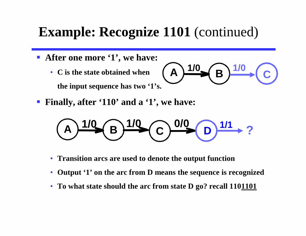
After one more ‘1’, we have:• C is the state obtained when
the input sequence has two ‘1’s.
Finally, after ‘110’ and a ‘1’, we have:
• Transition arcs are used to denote the output function
• Output ‘1’ on the arc from D means the sequence is recognized
• To what state should the arc from state D go? recall 1101101
Example: Recognize 1101 (continued)
A B1/0
A B1/0 C1/0 0/0
C1/0
D 1/1 ?
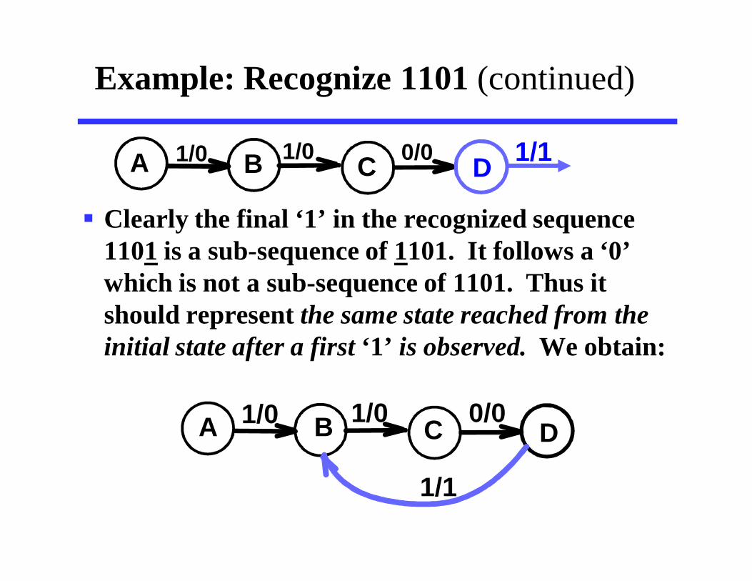
Example: Recognize 1101 (continued)
Clearly the final ‘1’ in the recognized sequence 1101 is a sub-sequence of 1101. It follows a ‘0’ which is not a sub-sequence of 1101. Thus it should represent the same state reached from the initial state after a first ‘1’ is observed. We obtain:
A B1/0 C1/0 0/0
DA B1/0 C1/0 0/0
1/1
D 1/1
Example: Recognize 1101 (continued)
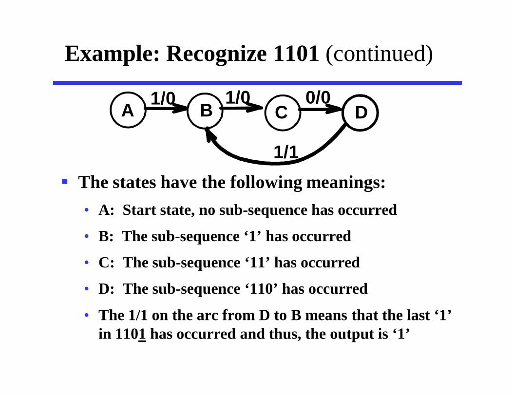
The states have the following meanings:• A: Start state, no sub-sequence has occurred
• B: The sub-sequence ‘1’ has occurred
• C: The sub-sequence ‘11’ has occurred
• D: The sub-sequence ‘110’ has occurred
• The 1/1 on the arc from D to B means that the last ‘1’ in 1101 has occurred and thus, the output is ‘1’
1/1
A B1/0C
1/0D
0/0
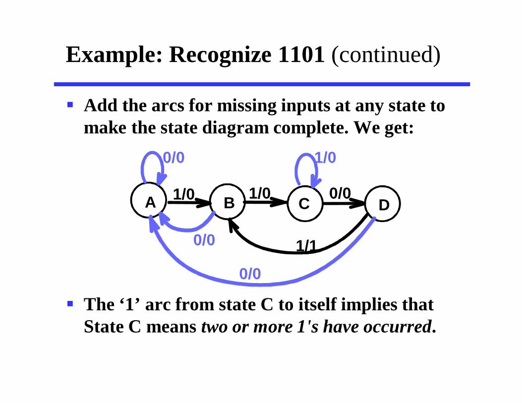
Example: Recognize 1101 (continued)
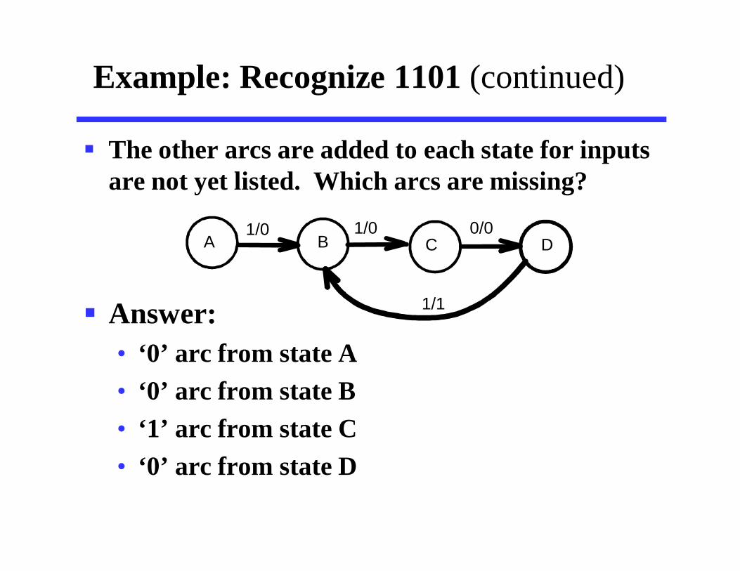
The other arcs are added to each state for inputs are not yet listed. Which arcs are missing?
Answer:• ‘0’ arc from state A• ‘0’ arc from state B• ‘1’ arc from state C• ‘0’ arc from state D
1/1
A B1/0
C1/0
D0/0
Example: Recognize 1101 (continued)
Add the arcs for missing inputs at any state to make the state diagram complete. We get:
The ‘1’ arc from state C to itself implies that State C means two or more 1's have occurred.
C
1/1
A B1/0 1/0D
0/0
0/0
0/0 1/0
0/0
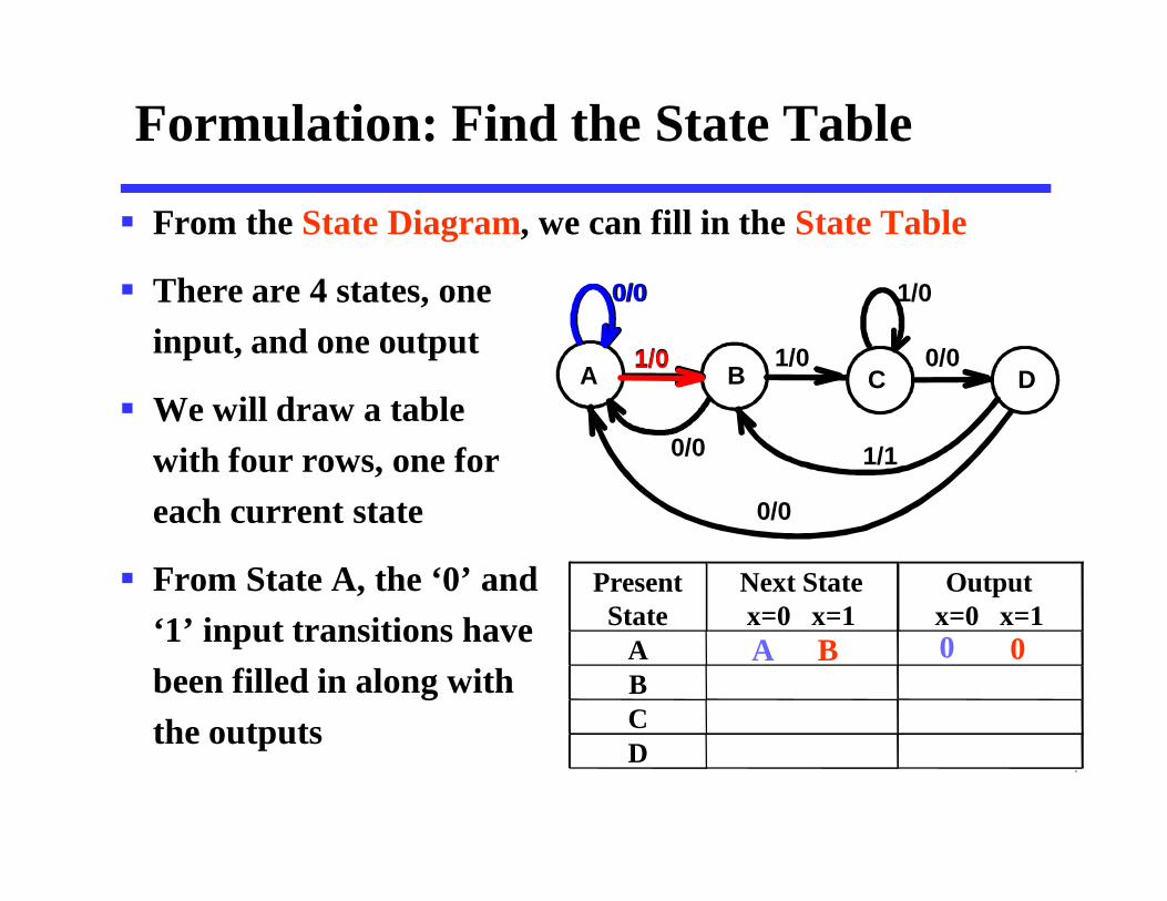
Formulation: Find the State Table
From the State Diagram, we can fill in the State Table
There are 4 states, oneinput, and one output
We will draw a tablewith four rows, one foreach current state
From State A, the ‘0’ and‘1’ input transitions havebeen filled in along withthe outputs
1/0
0/0
0/0
1/1
A B1/0
C1/0
D0/0
0/0
Present State
Next Statex=0 x=1
Outputx=0 x=1
ABCD
1/0
B 0
0/0
A 0
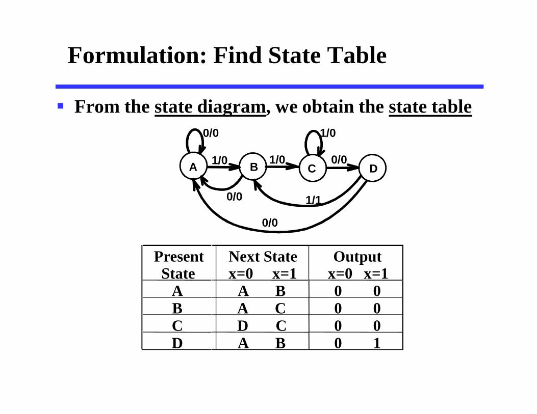
Formulation: Find State Table
From the state diagram, we obtain the state table1/00/0
0/0
0/0
1/1
A B1/0C
1/0D
0/0
StatePresent Next State
x=0 x=1Output
x=0 x=1A A B 0 0B A C 0 0C D C 0 0D A B 0 1
State Assignment
Each state must be assigned a unique code
Minimum number of bits required for m states in the state diagram is n such that
n ≥ log2 m , where x is the smallest integer ≥ x
There are useful state assignments that use more than the minimum number of bits
If n bits are used, there are 2n – m unused states
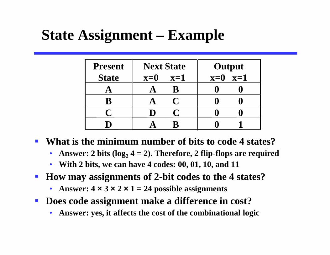
What is the minimum number of bits to code 4 states?• Answer: 2 bits (log2 4 = 2). Therefore, 2 flip-flops are required• With 2 bits, we can have 4 codes: 00, 01, 10, and 11
How may assignments of 2-bit codes to the 4 states?• Answer: 4 × 3 × 2 × 1 = 24 possible assignments
Does code assignment make a difference in cost?• Answer: yes, it affects the cost of the combinational logic
State Assignment – Example
Present State
Next Statex=0 x=1
Outputx=0 x=1
A A B 0 0B A C 0 0C D C 0 0D A B 0 1
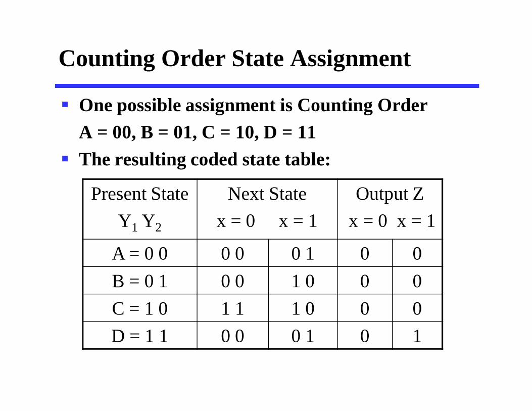
One possible assignment is Counting OrderA = 00, B = 01, C = 10, D = 11
The resulting coded state table:
Counting Order State Assignment
Present StateY1 Y2
Next Statex = 0 x = 1
Output Zx = 0 x = 1
A = 0 0 0 0 0 1 0 0B = 0 1 0 0 1 0 0 0C = 1 0 1 1 1 0 0 0D = 1 1 0 0 0 1 0 1
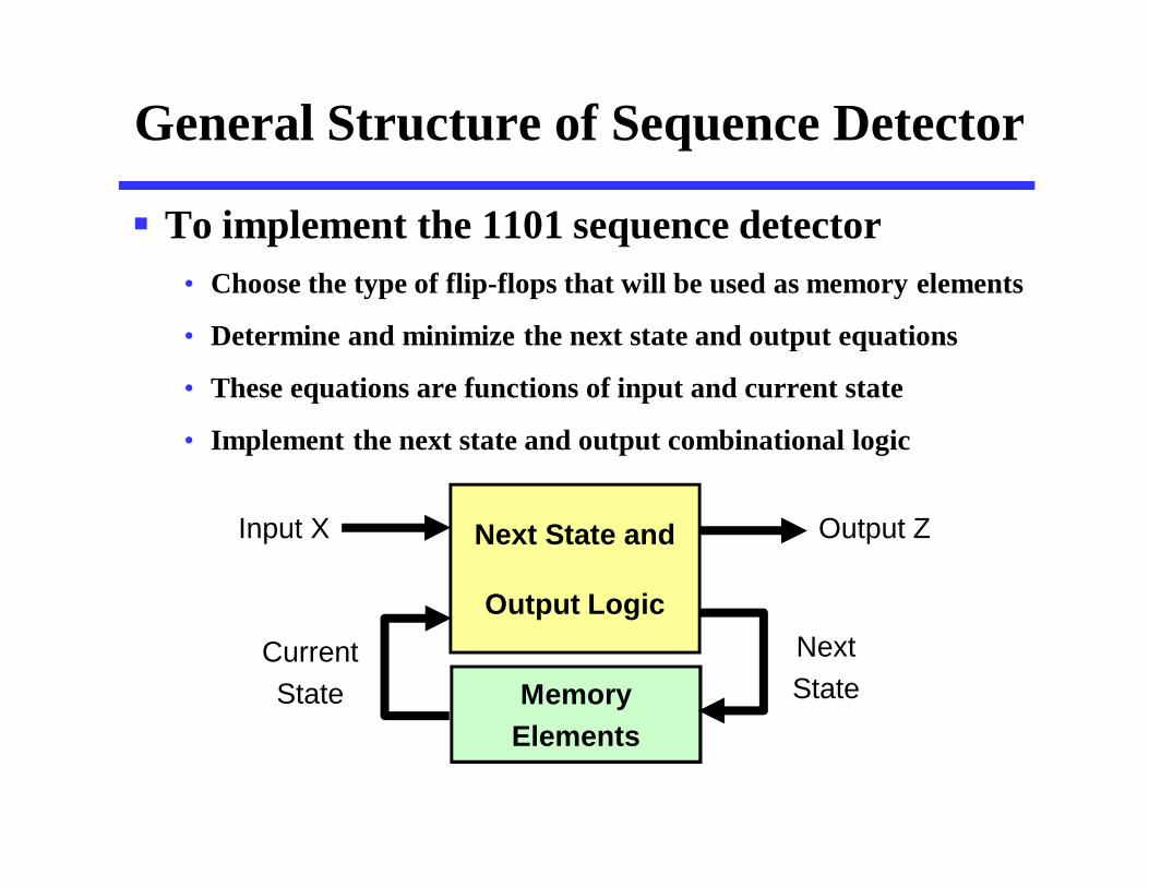
General Structure of Sequence Detector
To implement the 1101 sequence detector• Choose the type of flip-flops that will be used as memory elements
• Determine and minimize the next state and output equations
• These equations are functions of input and current state
• Implement the next state and output combinational logic
Next State and
Output Logic
MemoryElements
Input X Output Z
NextState
CurrentState
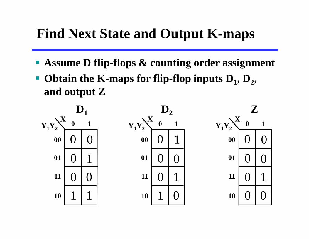
Find Next State and Output K-maps
D1 D2 Z
Assume D flip-flops & counting order assignment Obtain the K-maps for flip-flop inputs D1, D2,
and output Z
Y1Y2X
1
000
001
1
0 1
00
01
11
10
Y1Y2X
0
010
100
1
0 1
00
01
11
10
Y1Y2X
0
000
100
0
0 1
00
01
11
10
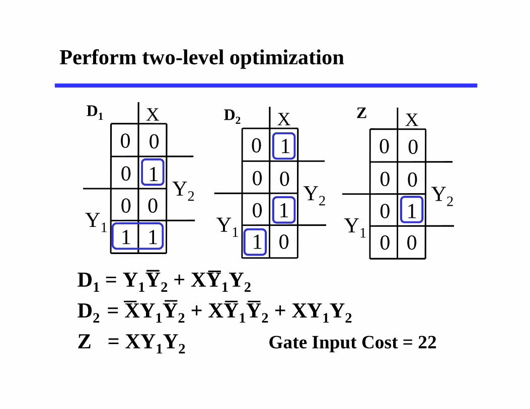
Perform two-level optimization
D1 = Y1Y2 + XY1Y2
D2 = XY1Y2 + XY1Y2 + XY1Y2
Z = XY1Y2 Gate Input Cost = 22
Y2
Y1
X
0
010
100
1
Y2
Y1
X
1
000
001
1
D1 D2 Z
Y2
Y1
X
0
000
100
0
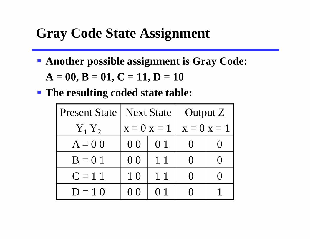
Another possible assignment is Gray Code:A = 00, B = 01, C = 11, D = 10 The resulting coded state table:
Gray Code State Assignment
Present StateY1 Y2
Next Statex = 0 x = 1
Output Zx = 0 x = 1
A = 0 0 0 0 0 1 0 0B = 0 1 0 0 1 1 0 0C = 1 1 1 0 1 1 0 0D = 1 0 0 0 0 1 0 1
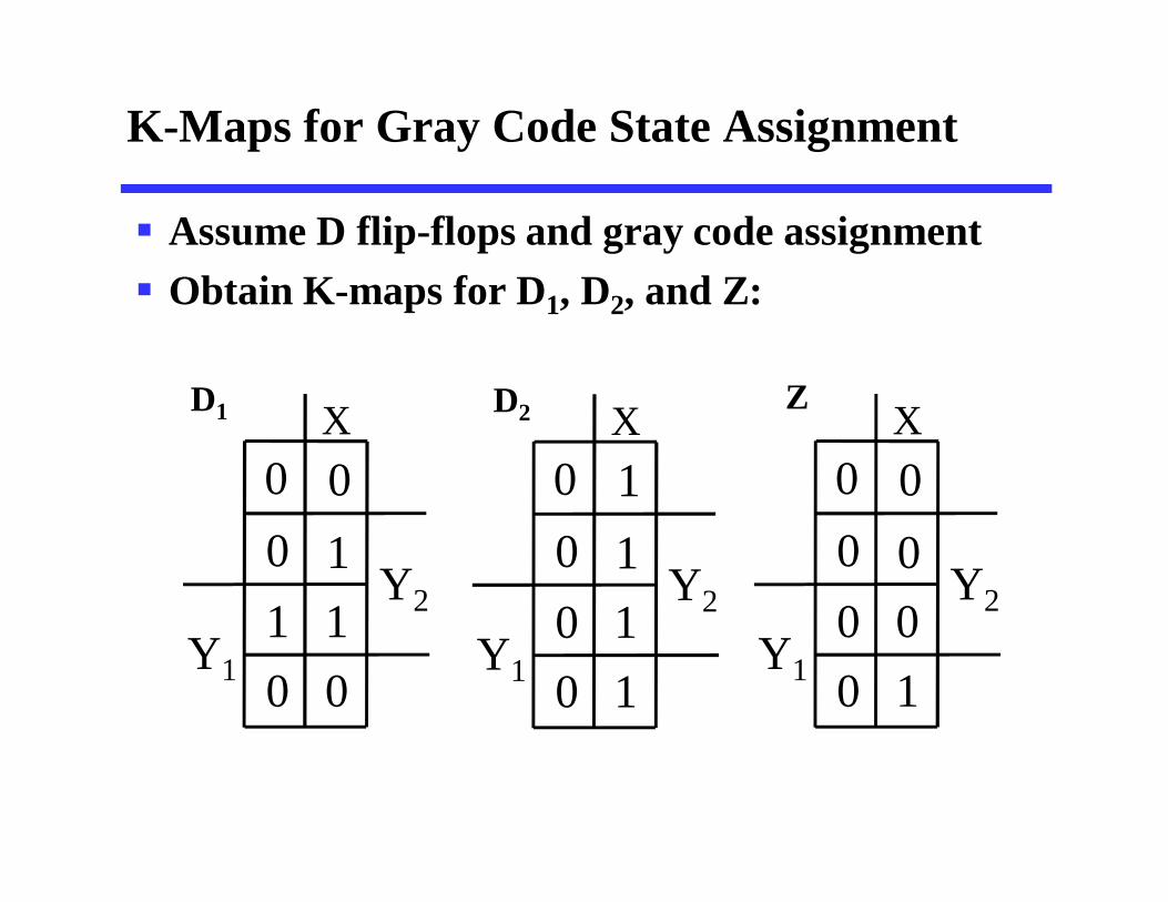
K-Maps for Gray Code State Assignment
Y2
Y1
X
1
000
000
0
Y2
Y1
X
1
010
101
0
Y2
Y1
X
0
000
111
0
Assume D flip-flops and gray code assignment Obtain K-maps for D1, D2, and Z:
D1 D2 Z
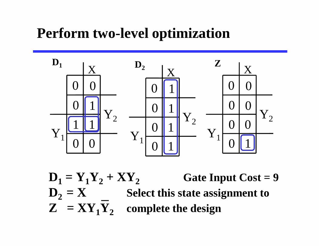
Perform two-level optimization
D1 = Y1Y2 + XY2 Gate Input Cost = 9D2 = X Select this state assignment toZ = XY1Y2 complete the design
Y2
Y1
X
1
000
000
0
Y2
Y1
X
1
010
101
0
Y2
Y1
X
0
000
111
0
D1 D2 Z
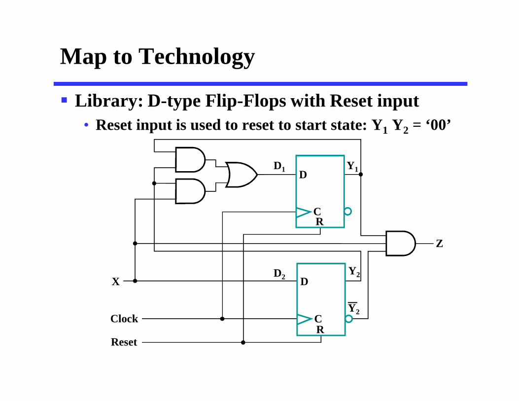
Library: D-type Flip-Flops with Reset input• Reset input is used to reset to start state: Y1 Y2 = ‘00’
Map to Technology
Clock
D
D
CR
Y2
Z
CR
Y1
X
Reset
Y2
D1
D2
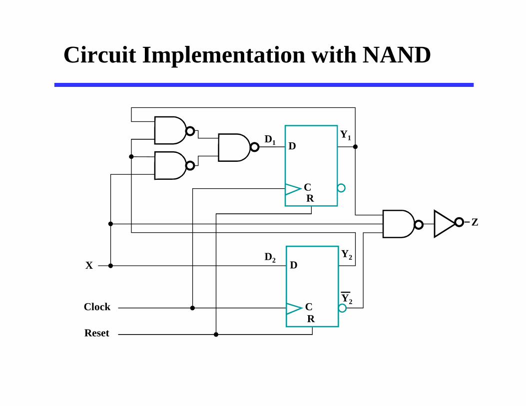
Circuit Implementation with NAND
Clock
D
D
CR
Y2
Z
CR
Y1
X
Reset
Y2
D1
D2
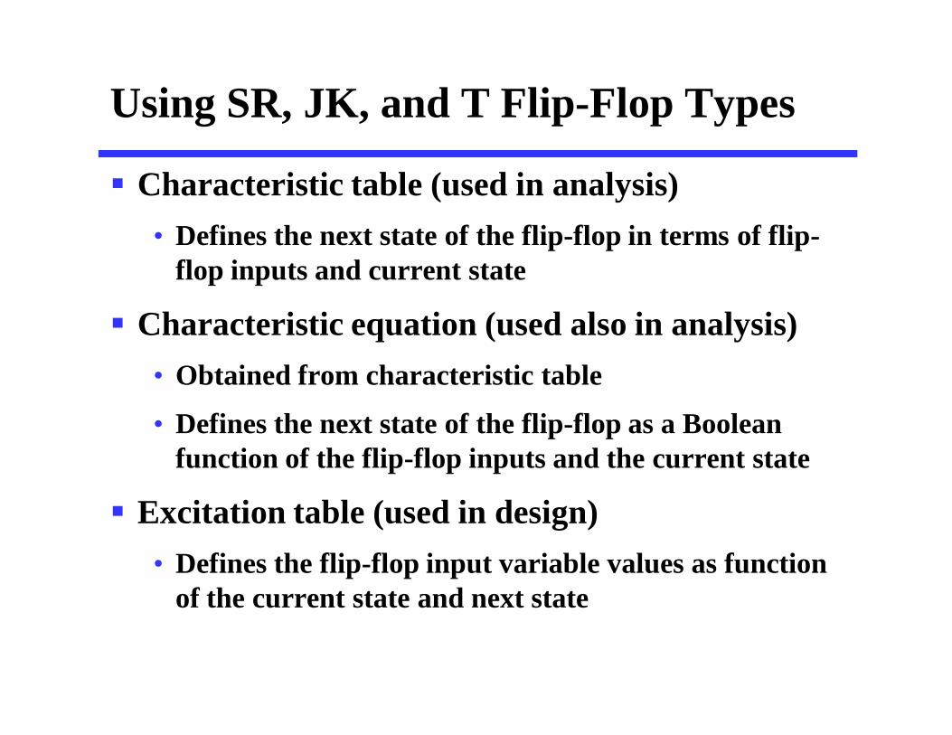
Using SR, JK, and T Flip-Flop Types
Characteristic table (used in analysis)• Defines the next state of the flip-flop in terms of flip-
flop inputs and current state
Characteristic equation (used also in analysis)• Obtained from characteristic table
• Defines the next state of the flip-flop as a Boolean function of the flip-flop inputs and the current state
Excitation table (used in design)• Defines the flip-flop input variable values as function
of the current state and next state
Characteristic EquationQ(t+1) = S + R Q(t)S R = 0 (S and R cannot be 1 simultaneously)
SR Flip-Flop
Characteristic Table
Excitation TableOperation
No changeSetReset
No change
S
X
010
Q(t+1)
01
1
0
Q(t)
00
1
1
R
X01
0
001
1
OperationS
010
1
R
No changeResetSet
Undefined
01
?
Q(t+1)
Q(t)
S
C
R
Symbol
Q
Q
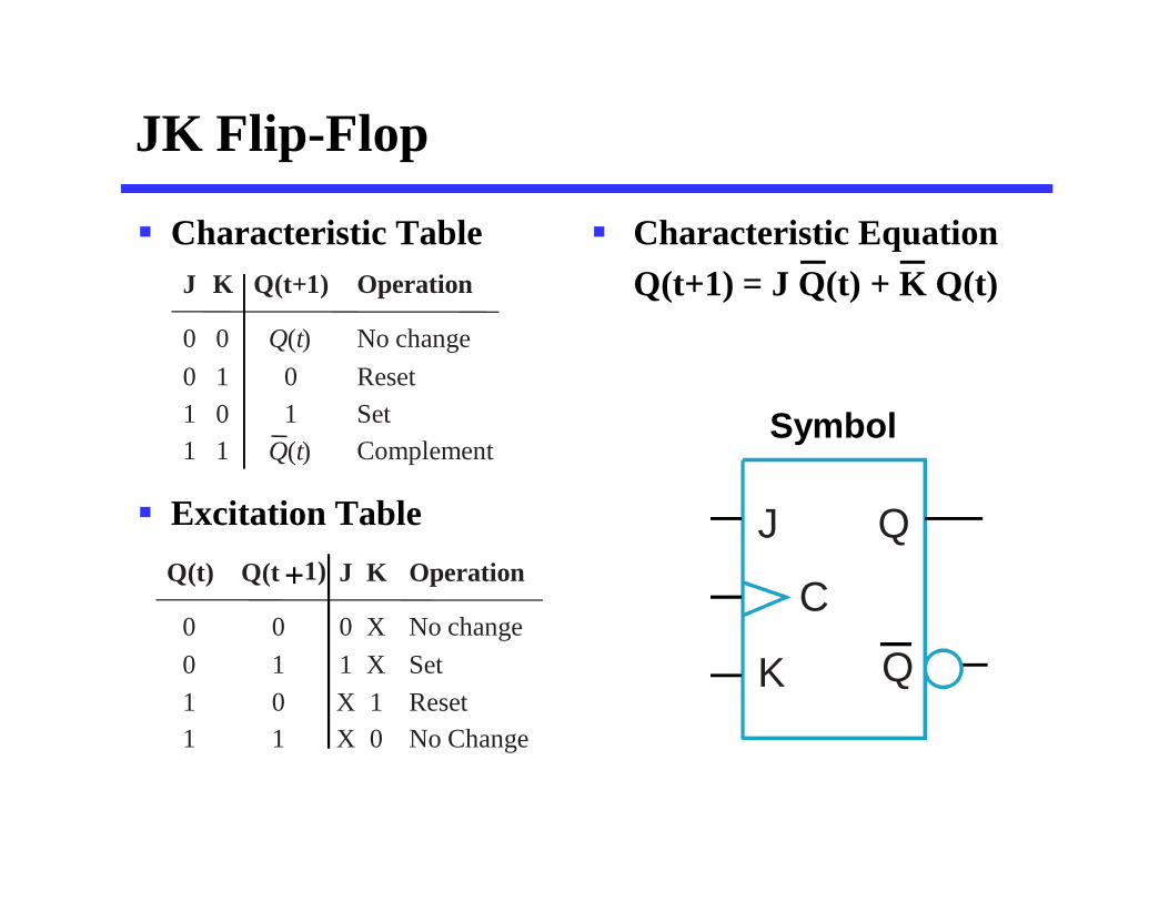
JK Flip-Flop
Characteristic Table
Excitation Table J
C
K
Symbol
Q
Q
0011
No change
SetReset
Complement
OperationJ
0101
K
01
Q(t+1)
Q(t)
Q(t)
Q(t +1)
01
10
Q(t)
00
11
Operation
XX
01
K
01
XX
J
No changeSetResetNo Change
Characteristic EquationQ(t+1) = J Q(t) + K Q(t)
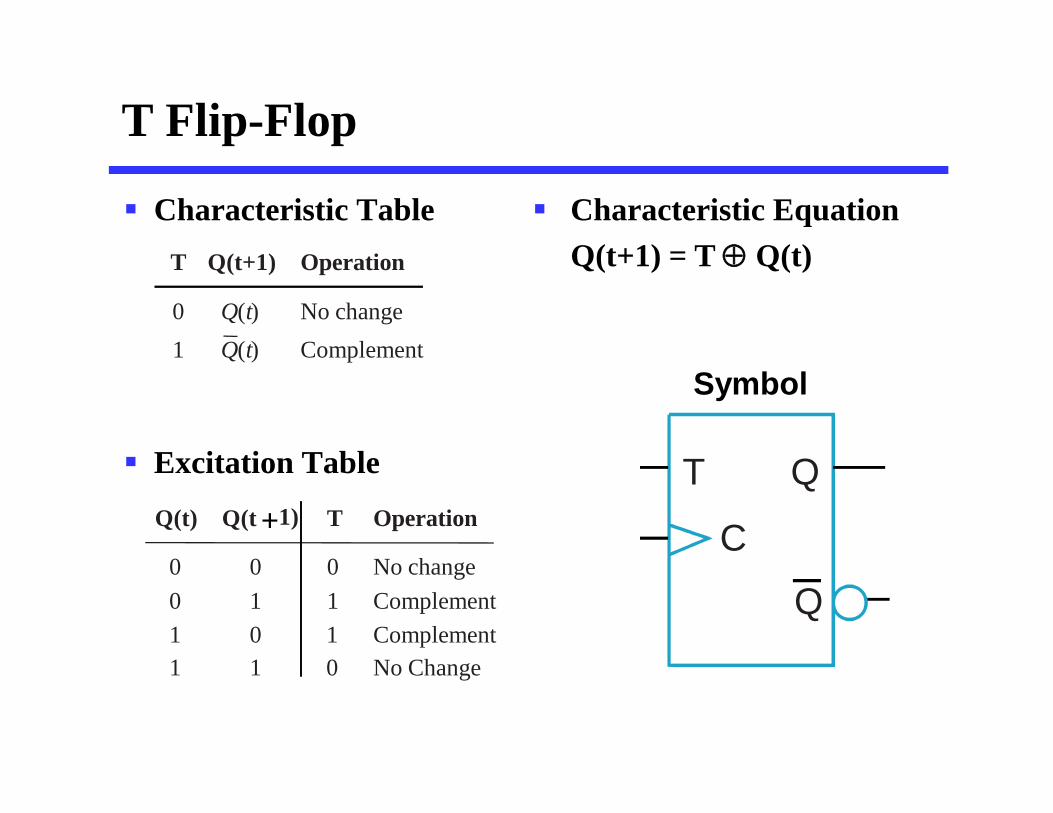
T Flip-Flop
Characteristic Table
Excitation Table T
C
Symbol
Q
Q
Characteristic EquationQ(t+1) = T Q(t)
No changeComplement
Operation
01
T Q(t+1)
Q(t)Q(t)
Q(t +1)
01
10
Q(t)
00
11
Operation
01
01
T
No changeComplementComplementNo Change
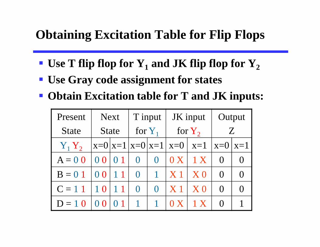
Obtaining Excitation Table for Flip Flops
Use T flip flop for Y1 and JK flip flop for Y2
Use Gray code assignment for states Obtain Excitation table for T and JK inputs:
PresentState
NextState
T inputfor Y1
JK inputfor Y2
OutputZ
Y1 Y2 x=0 x=1 x=0 x=1 x=0 x=1 x=0 x=1A = 0 0 0 0 0 1 0 0 0 X 1 X 0 0B = 0 1 0 0 1 1 0 1 X 1 X 0 0 0C = 1 1 1 0 1 1 0 0 X 1 X 0 0 0D = 1 0 0 0 0 1 1 1 0 X 1 X 0 1
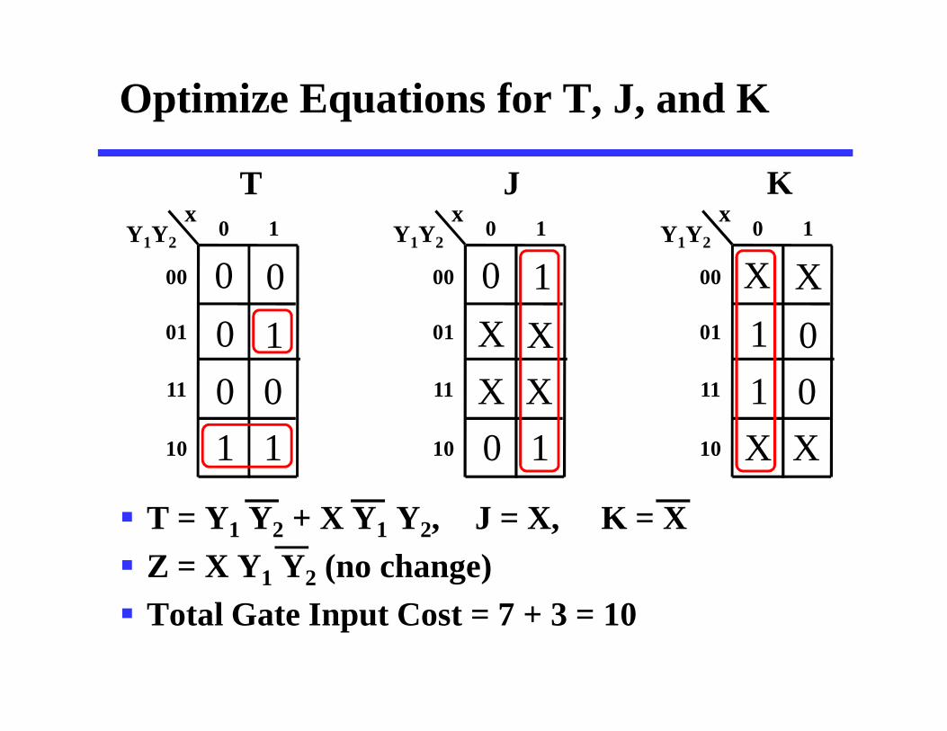
Optimize Equations for T, J, and K
T = Y1 Y2 + X Y1 Y2, J = X, K = X Z = X Y1 Y2 (no change) Total Gate Input Cost = 7 + 3 = 10
T J KY1Y2
x
1
000
001
1
0 1
00
01
11
10
Y1Y2x
1
X10
XXX
0
0 1
00
01
11
10
Y1Y2x
X
1XX
010
X
0 1
00
01
11
10
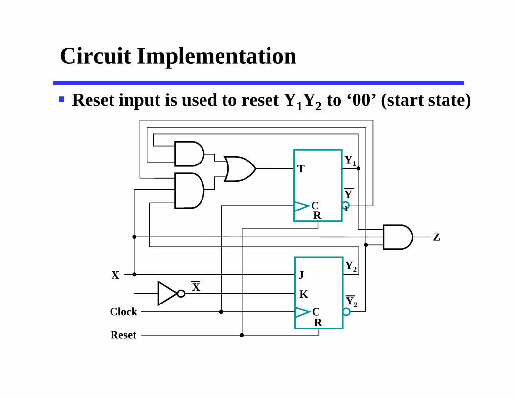
Reset input is used to reset Y1Y2 to ‘00’ (start state)
Circuit Implementation
Clock
T
J
CR
Y2
Z
CR
Y1
X
Reset
Y2KX
Y1
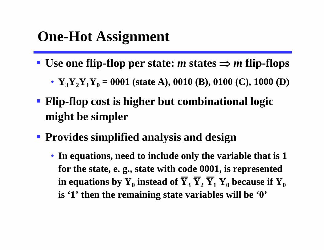
One-Hot Assignment
Use one flip-flop per state: m states m flip-flops• Y3Y2Y1Y0 = 0001 (state A), 0010 (B), 0100 (C), 1000 (D)
Flip-flop cost is higher but combinational logic might be simpler
Provides simplified analysis and design• In equations, need to include only the variable that is 1
for the state, e. g., state with code 0001, is represented in equations by Y0 instead of Y3 Y2 Y1 Y0 because if Y0is ‘1’ then the remaining state variables will be ‘0’
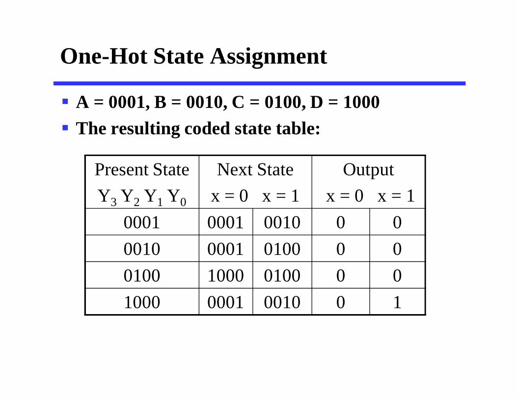
A = 0001, B = 0010, C = 0100, D = 1000 The resulting coded state table:
One-Hot State Assignment
Present StateY3 Y2 Y1 Y0
Next Statex = 0 x = 1
Outputx = 0 x = 1
0001 0001 0010 0 00010 0001 0100 0 00100 1000 0100 0 01000 0001 0010 0 1
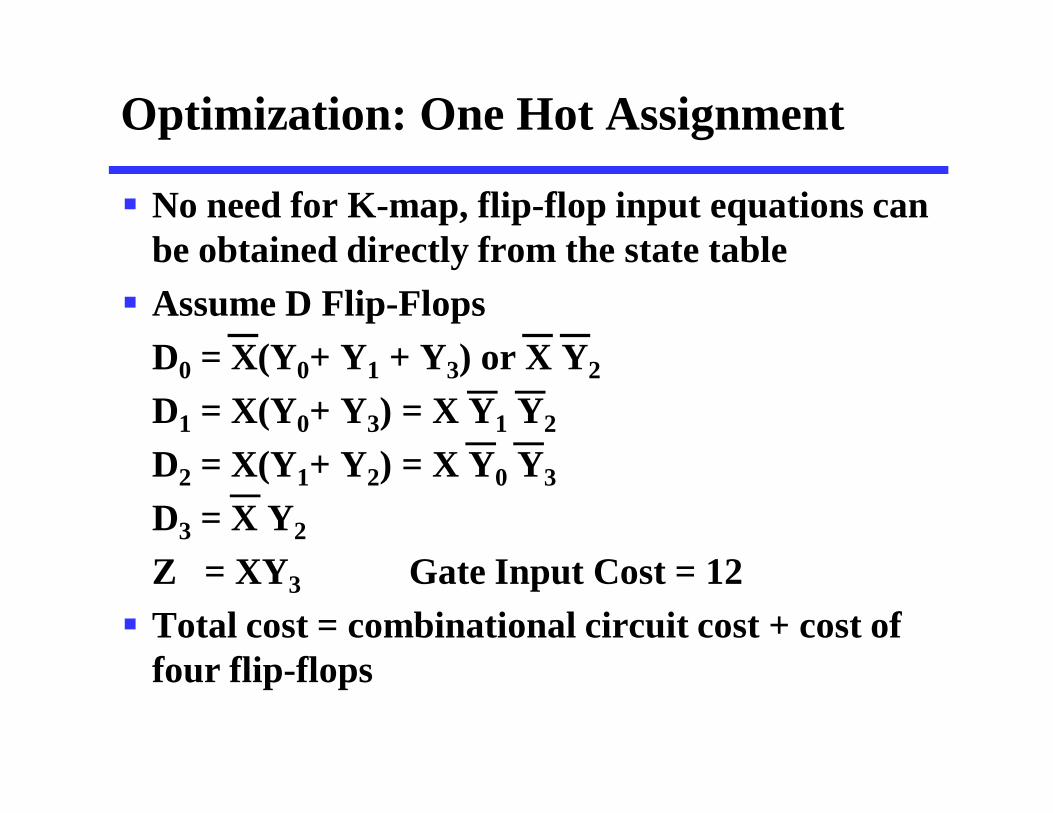
Optimization: One Hot Assignment
No need for K-map, flip-flop input equations can be obtained directly from the state table Assume D Flip-Flops
D0 = X(Y0+ Y1 + Y3) or X Y2
D1 = X(Y0+ Y3) = X Y1 Y2
D2 = X(Y1+ Y2) = X Y0 Y3
D3 = X Y2
Z = XY3 Gate Input Cost = 12 Total cost = combinational circuit cost + cost of
four flip-flops
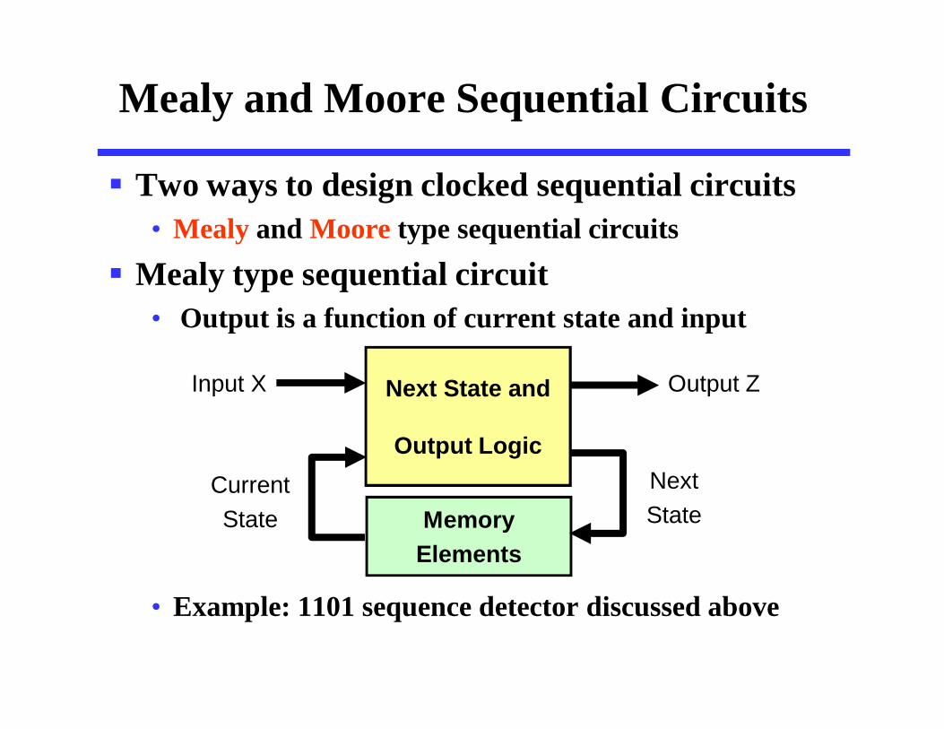
Mealy and Moore Sequential Circuits
Two ways to design clocked sequential circuits• Mealy and Moore type sequential circuits
Mealy type sequential circuit• Output is a function of current state and input
• Example: 1101 sequence detector discussed above
Next State and
Output Logic
MemoryElements
Input X Output Z
NextState
CurrentState
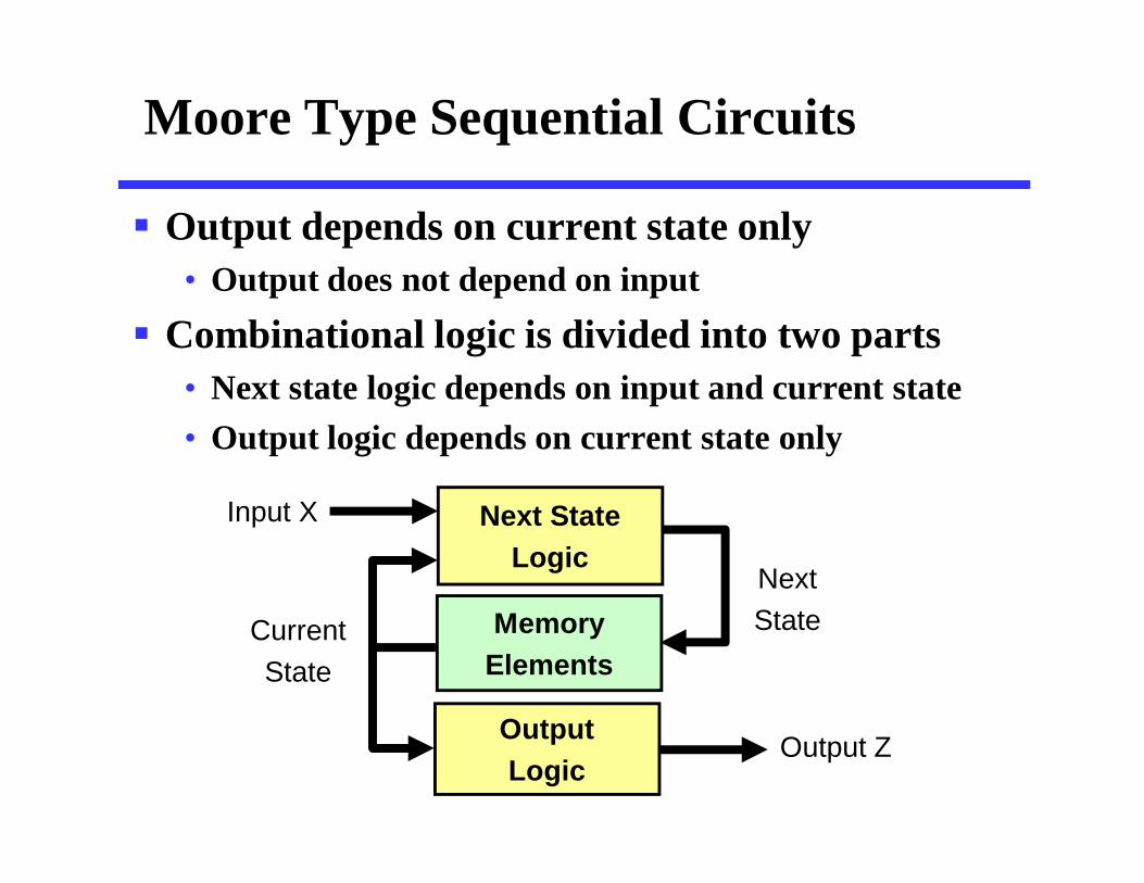
Moore Type Sequential Circuits
Output depends on current state only• Output does not depend on input
Combinational logic is divided into two parts• Next state logic depends on input and current state• Output logic depends on current state only
Next StateLogic
MemoryElements
Input X
Output Z
NextStateCurrent
State
OutputLogic
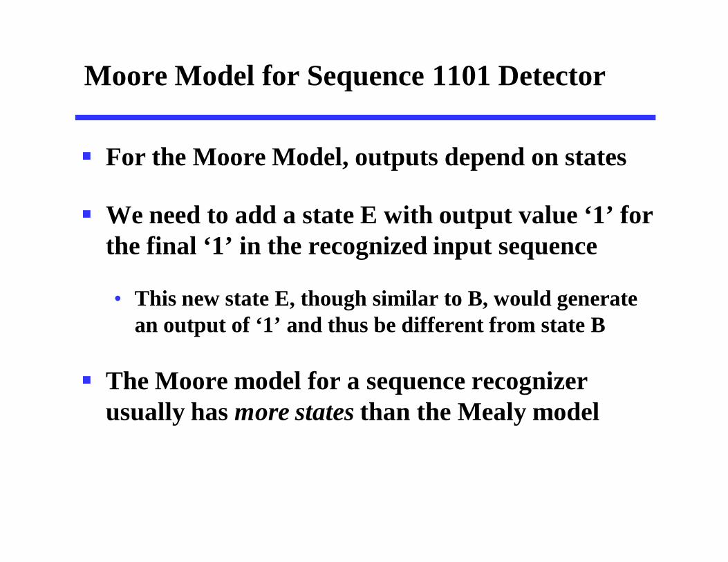
Moore Model for Sequence 1101 Detector
For the Moore Model, outputs depend on states
We need to add a state E with output value ‘1’ for the final ‘1’ in the recognized input sequence
• This new state E, though similar to B, would generate an output of ‘1’ and thus be different from state B
The Moore model for a sequence recognizer usually has more states than the Mealy model
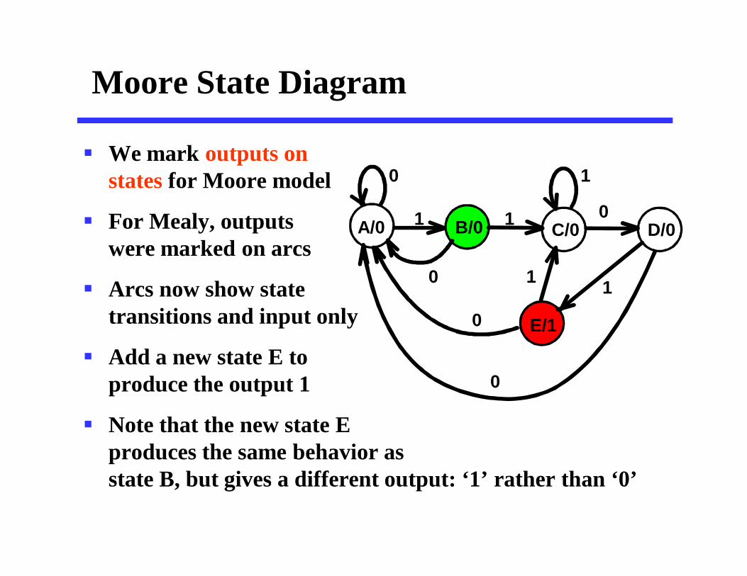
Moore State Diagram
We mark outputs onstates for Moore model
For Mealy, outputswere marked on arcs
Arcs now show statetransitions and input only
Add a new state E toproduce the output 1
Note that the new state Eproduces the same behavior asstate B, but gives a different output: ‘1’ rather than ‘0’
A/0 B/0 C/0 D/0
0
E/1
0
0
0
11
1
110
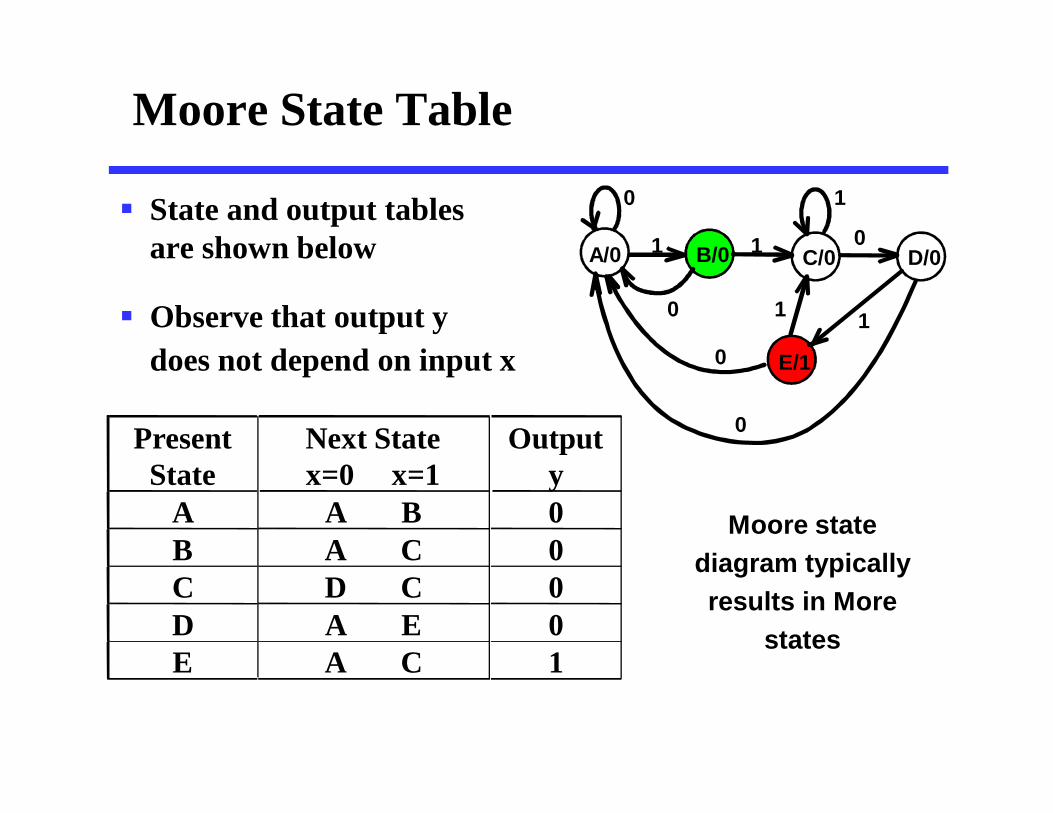
Moore State Table
State and output tablesare shown below
Observe that output ydoes not depend on input x
A/0 B/0 C/0 D/0
0
E/1
0
0
0
11
1
110
Present State
Next Statex=0 x=1
Outputy
A A B 0B A C 0C D C 0D A E 0E A C 1
Moore state diagram typically results in More
states
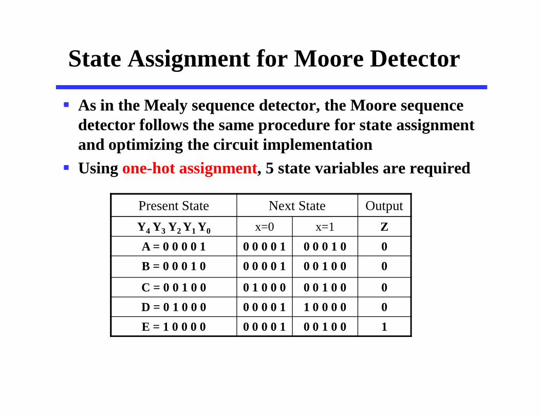
State Assignment for Moore Detector
As in the Mealy sequence detector, the Moore sequence detector follows the same procedure for state assignment and optimizing the circuit implementation
Using one-hot assignment, 5 state variables are required
Present State Next State OutputY4 Y3 Y2 Y1 Y0 x=0 x=1 ZA = 0 0 0 0 1 0 0 0 0 1 0 0 0 1 0 0B = 0 0 0 1 0 0 0 0 0 1 0 0 1 0 0 0
C = 0 0 1 0 0 0 1 0 0 0 0 0 1 0 0 0D = 0 1 0 0 0 0 0 0 0 1 1 0 0 0 0 0E = 1 0 0 0 0 0 0 0 0 1 0 0 1 0 0 1
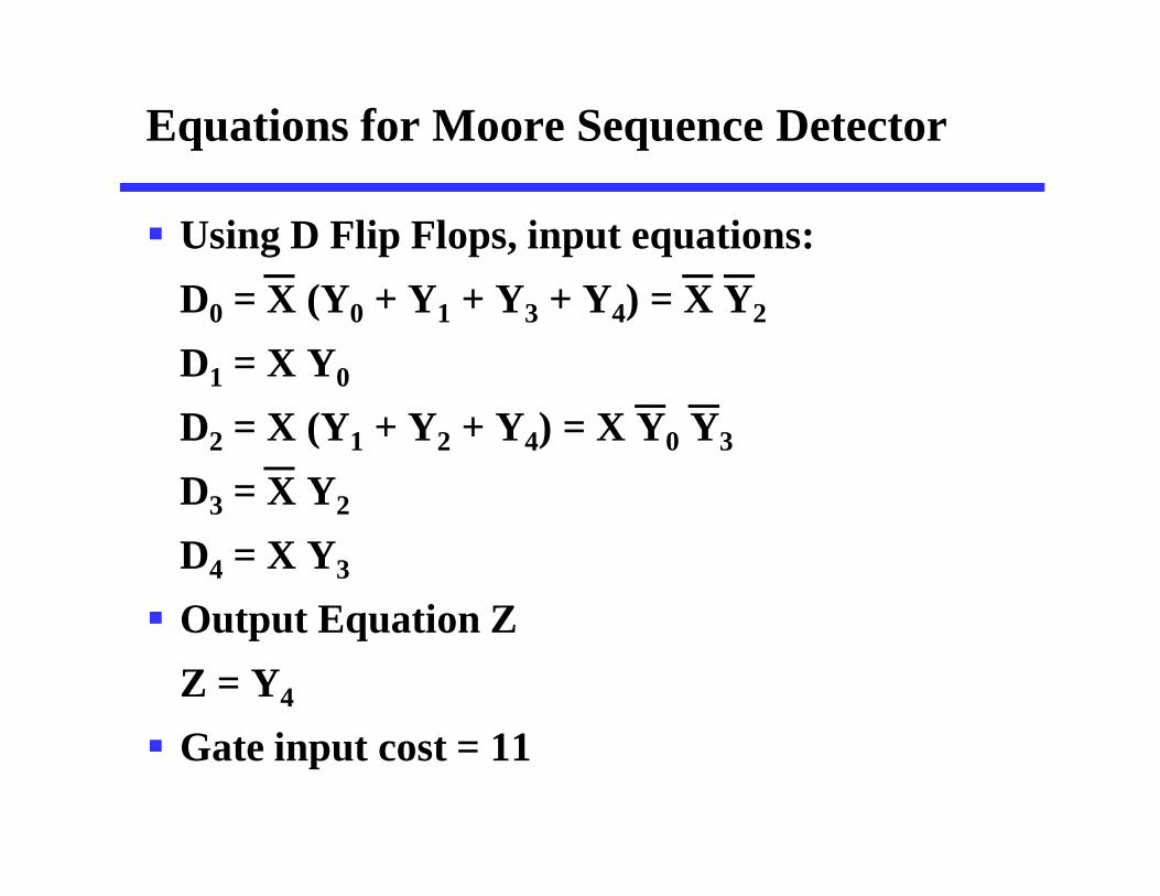
Equations for Moore Sequence Detector
Using D Flip Flops, input equations:D0 = X (Y0 + Y1 + Y3 + Y4) = X Y2
D1 = X Y0
D2 = X (Y1 + Y2 + Y4) = X Y0 Y3
D3 = X Y2
D4 = X Y3
Output Equation ZZ = Y4
Gate input cost = 11
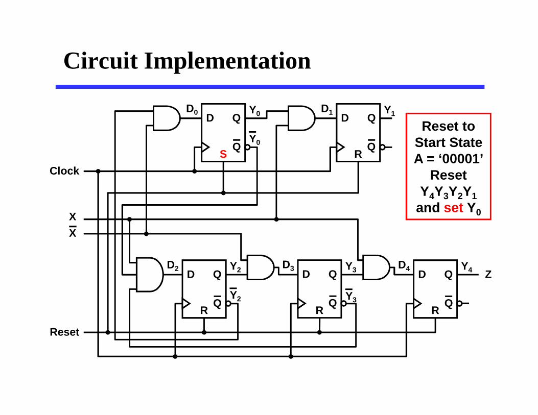
Circuit Implementation
D2 Y2D Q
QR
D4 Y4D Q
QR
D3 Y3D Q
QR
Z
XX
D0 Y0D Q
QS
Y2 Y3
D1 Y1D Q
QRY0
Reset
Clock
Reset toStart StateA = ‘00001’
ResetY4Y3Y2Y1
and set Y0
Verification
Sequential circuits should be verified by showing that the circuit produces the original state diagram
Verification can be done manually, or with the help of a simulation program
All possible input combinations are applied at each state and the state variables and outputs are observed
A reset input is used to reset the circuit to its initial state
Apply a sequence of inputs to test all the state-input combinations, i.e., all transitions in the state diagram
Observe the output and the next state that appears after each clock edge in the timing diagram
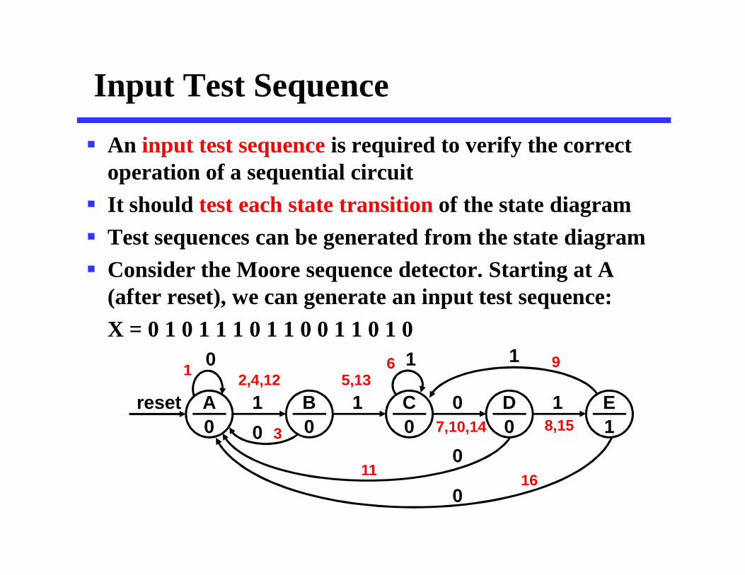
Input Test Sequence An input test sequence is required to verify the correct
operation of a sequential circuit It should test each state transition of the state diagram Test sequences can be generated from the state diagram Consider the Moore sequence detector. Starting at A
(after reset), we can generate an input test sequence:X = 0 1 0 1 1 1 0 1 1 0 0 1 1 0 1 0
1 1 0reset
0 1
00
1A0
B0
C0
D0
E1
0
1
7,10,14
1 2,4,12 5,13
3
11
6
8,15
9
16
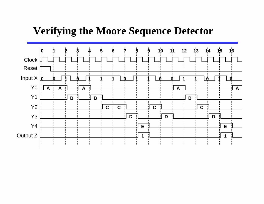
Verifying the Moore Sequence Detector
ClockReset
0 1 2 3 4 5 6 7 8 9 10 11 12 13 14 15 16
Input X 0 0 1 0 1 1 1 0 1 1 0 0 1 1 0 1 0
Y0
Y1
Y2
Y3
Y4
Output Z
A A A A A
B B B
C C C C
D D D
E E
1 1
Moore versus Mealy Sequential Circuits
Output in a Moore sequential circuit is associated with astate, while output in a Mealy circuit is associated with atransition between states
In general, Moore state diagrams have more states than corresponding Mealy state diagrams and the Moore sequential circuit implementation might have higher cost
Since the output in a Mealy machine is a combination of present state and input values, an unsynchronized input may result in an invalid output (drawback of Mealy)
A Moore state diagram produces a unique output for every state irrespective of inputs. Output of a Moore machine is synchronized with the clock (better)
1
0
1/1
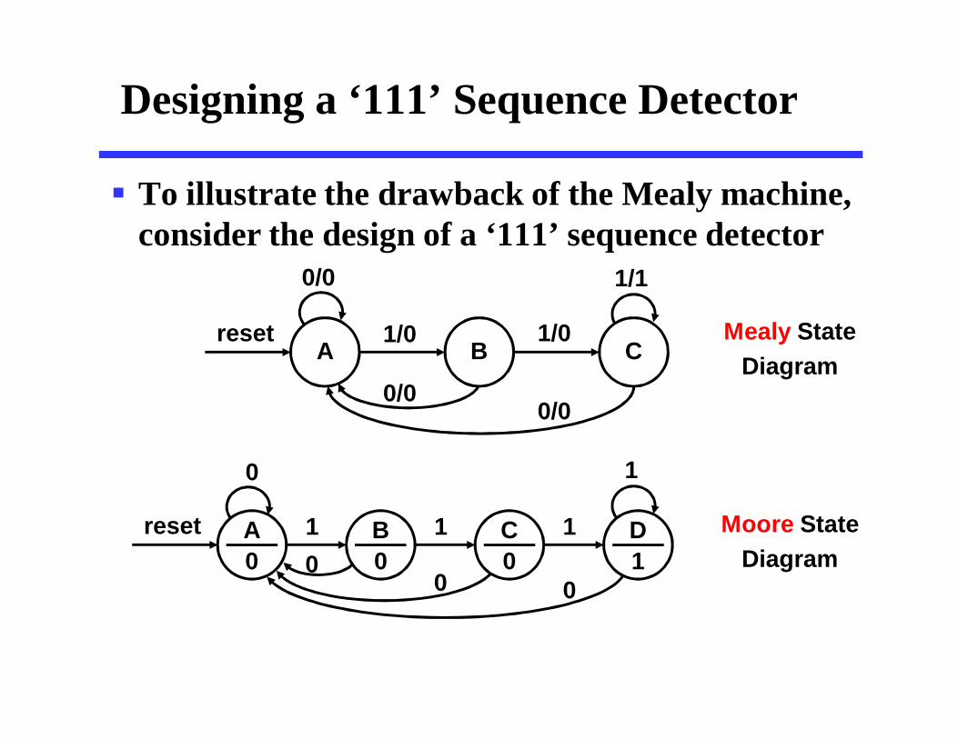
Designing a ‘111’ Sequence Detector
To illustrate the drawback of the Mealy machine, consider the design of a ‘111’ sequence detector
B1/0
C1/0
0/00/0
0/0
Areset Mealy State
Diagram
C0
1 D1
1A0
reset
0
B0
10
0
Moore State Diagram
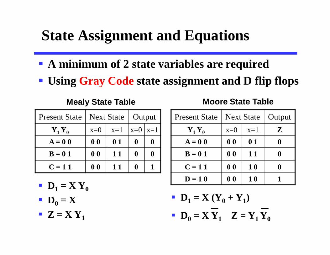
State Assignment and Equations
A minimum of 2 state variables are required Using Gray Code state assignment and D flip flops
Present State Next State OutputY1 Y0 x=0 x=1 Z
A = 0 0 0 0 0 1 0B = 0 1 0 0 1 1 0
C = 1 1 0 0 1 0 0D = 1 0 0 0 1 0 1
Present State Next State OutputY1 Y0 x=0 x=1 x=0 x=1
A = 0 0 0 0 0 1 0 0B = 0 1 0 0 1 1 0 0
C = 1 1 0 0 1 1 0 1
Mealy State Table Moore State Table
D1 = X Y0
D0 = X Z = X Y1
D1 = X (Y0 + Y1)
D0 = X Y1 Z = Y1 Y0
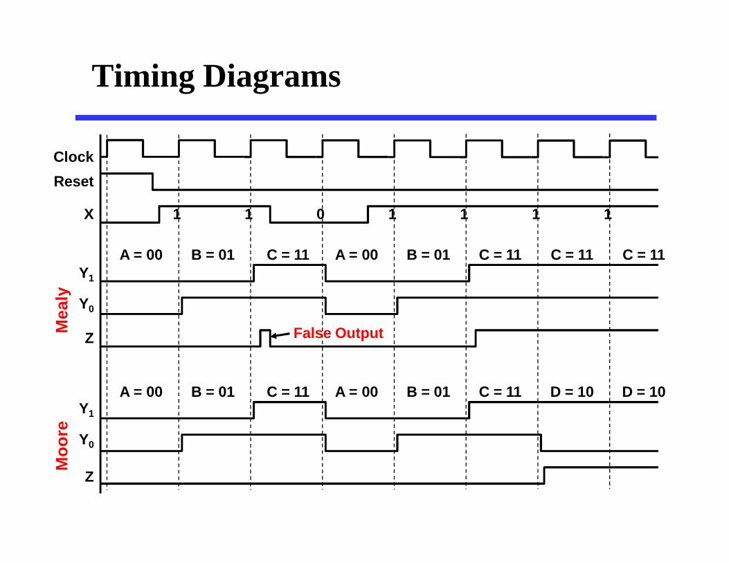
Timing Diagrams
ClockReset
X 1 1 0 1 1 1 1
Y1
Y0
Z
Y1
Y0
Z
Mea
lyM
oore
C = 11A = 00 B = 01 A = 00 B = 01 C = 11 C = 11 C = 11
C = 11A = 00 B = 01 A = 00 B = 01 C = 11 D = 10 D = 10
False Output


![2012_MC9211[2]_ sequential Circuit](https://static.fdocuments.net/doc/165x107/55cf9b8b550346d033a67a2a/2012mc92112-sequential-circuit.jpg)


