Sensors and Actuators B: Chemical · 2015-03-01 · Sensors and Actuators B: Chemical journal...
8
Sensors and Actuators B 186 (2013) 1–8 Contents lists available at SciVerse ScienceDirect Sensors and Actuators B: Chemical journal h om epage: www.elsevier.com/locat e/snb The dual role of Parylene C in chemical sensing: Acting as an encapsulant and as a sensing membrane for pH monitoring applications Tatiana Trantidou a,∗ , David J. Payne b , Vasileios Tsiligkiridis a , Yu-Chun Chang a , Christofer Toumazou a , Themistoklis Prodromakis a,c a Centre for Bio-Inspired Technology, Department of Electrical and Electronic Engineering, Imperial College London, London SW7 2AZ, UK b Department of Materials, Imperial College London, SW7 2AZ, UK c Nano Research Group, Department of Electronics and Computer Science, University of Southampton, SO17 1BJ, UK a r t i c l e i n f o Article history: Received 18 February 2013 Received in revised form 24 April 2013 Accepted 21 May 2013 Available online 30 May 2013 Keywords: Parylene C Chemical sensing membrane pH monitoring Oxygen plasma Extended gate Discrete MOSFETs a b s t r a c t In this work, we demonstrate a new property of Parylene C emphasizing on its application in pH sensing technologies. For many decades the material has been extensively used as a biocompatible inert encap- sulant of implantable micro-devices. Toward a new understanding of the material’s potential, we explore the transformation of Parylene C from a passive encapsulation membrane into an active H + sensing mem- brane using discrete MOSFETs to evaluate its chemical sensing performance. We employ oxygen plasma treatment to functionalize Parylene’s H + sensing capacity and enhance the chemical sensitivity, drift rates, and reliability of the sensing devices. Moreover, we demonstrate a versatile technique that enables the deployment of the material both as an encapsulant and as a sensing membrane in a single platform, in order to benefit from distinguishable and consistent sensitivities, and low leakage currents during pH measurements. Our investigation reveals that the selective modification of Parylene’s surface chemistry yields reliable pH sensing devices, ensuring the best combination of sensitivity (16.3 mV/pH) and leak- age currents (6–10 nA) over a reasonably wide pH range (4–10), while drift rates remain in low levels (2.5–20 mV/h). We believe that this study opens up new application horizons for Parylene, which is a new promising material in the emerging field of flexible electronics able to deliver low film thicknesses and high biocompatibility, while facilitating the application of mechanical stimulus. © 2013 Elsevier B.V. All rights reserved. 1. Introduction Over the past few decades, poly(chloro-para-xylynene) (Pary- lene C) has been extensively used as a biocompatible encapsulant (barrier medium) of implantable microdevices, such as pace- makers [1] and catheters [2], chemical sensors [3,4], probes [5] and microelectrodes [6]. Parylene’s excellent encapsulation prop- erties have been attributed to its pinhole free nature above 100 nm [7], acting as an electrolyte-barrier layer, but also to its hydrophobic surface, resulting in the retraction of electrolytes that come in contact. Besides its numerous encapsulation applica- tions, Parylene has been also employed together with ion-sensitive field effect transistors (ISFETs) to suppress their pH sensitivity and serve as solid state reference electrodes, namely reference field-effect-transistors (REFETs), for differential ISFET/REFET pH measurements. The concept of the Parylene REFET has been ∗ Corresponding author. Tel.: +44 20 7594 0840. E-mail address: [email protected] (T. Trantidou). introduced by Matsuo et al. [8], who attempted to deposit a thin film of Parylene on a Si 3 N 4 -gate ISFET in order to render it chemi- cally inert. Nonetheless, the pH response of the Parylene-gate ISFET showed a maximum sensitivity of 28 mV/pH below pH 4, whereas for larger pH values the sensor was ion insensitive. Chemical mod- ification of Parylene’s surface with crown ether compounds was also implemented to examine the K + sensitivity of the REFET, nev- ertheless, problems such as decreasing ionic sensitivity response over time and large drift were reported. The electrostatic coupling between the ions and the gate insu- lating membrane has been the fundamental functional principle for a variety of well-established H + sensing technologies. This princi- ple is mathematically expressed by the equation of electrostatics derived from Coulomb’s law stating that the magnitude of the electric field created by a distribution of charges is inversely propor- tional to the dielectric thickness. This has been also proven by our recent work which demonstrated that thinner passivations result in an increase of the electrostatic coupling of H + and, therefore, in an improved sensitivity of the ISFET sensors [9]. This functional prop- erty has also been exploited for a different reason; to improve the 0925-4005/$ – see front matter © 2013 Elsevier B.V. All rights reserved. http://dx.doi.org/10.1016/j.snb.2013.05.077
Transcript of Sensors and Actuators B: Chemical · 2015-03-01 · Sensors and Actuators B: Chemical journal...
Tea
TCa
b
c
ARRAA
KPCpOED
1
l(mae1httfiafim
0h
Sensors and Actuators B 186 (2013) 1– 8
Contents lists available at SciVerse ScienceDirect
Sensors and Actuators B: Chemical
journa l h om epage: www.elsev ier .com/ locat e/snb
he dual role of Parylene C in chemical sensing: Acting as anncapsulant and as a sensing membrane for pH monitoringpplications
atiana Trantidoua,∗, David J. Payneb, Vasileios Tsiligkiridisa, Yu-Chun Changa,hristofer Toumazoua, Themistoklis Prodromakisa,c
Centre for Bio-Inspired Technology, Department of Electrical and Electronic Engineering, Imperial College London, London SW7 2AZ, UKDepartment of Materials, Imperial College London, SW7 2AZ, UKNano Research Group, Department of Electronics and Computer Science, University of Southampton, SO17 1BJ, UK
a r t i c l e i n f o
rticle history:eceived 18 February 2013eceived in revised form 24 April 2013ccepted 21 May 2013vailable online 30 May 2013
eywords:arylene Chemical sensing membraneH monitoring
a b s t r a c t
In this work, we demonstrate a new property of Parylene C emphasizing on its application in pH sensingtechnologies. For many decades the material has been extensively used as a biocompatible inert encap-sulant of implantable micro-devices. Toward a new understanding of the material’s potential, we explorethe transformation of Parylene C from a passive encapsulation membrane into an active H+ sensing mem-brane using discrete MOSFETs to evaluate its chemical sensing performance. We employ oxygen plasmatreatment to functionalize Parylene’s H+ sensing capacity and enhance the chemical sensitivity, driftrates, and reliability of the sensing devices. Moreover, we demonstrate a versatile technique that enablesthe deployment of the material both as an encapsulant and as a sensing membrane in a single platform,in order to benefit from distinguishable and consistent sensitivities, and low leakage currents during pH
xygen plasmaxtended gateiscrete MOSFETs
measurements. Our investigation reveals that the selective modification of Parylene’s surface chemistryyields reliable pH sensing devices, ensuring the best combination of sensitivity (16.3 mV/pH) and leak-age currents (6–10 nA) over a reasonably wide pH range (4–10), while drift rates remain in low levels(2.5–20 mV/h). We believe that this study opens up new application horizons for Parylene, which is anew promising material in the emerging field of flexible electronics able to deliver low film thicknessesand high biocompatibility, while facilitating the application of mechanical stimulus.
. Introduction
Over the past few decades, poly(chloro-para-xylynene) (Pary-ene C) has been extensively used as a biocompatible encapsulantbarrier medium) of implantable microdevices, such as pace-
akers [1] and catheters [2], chemical sensors [3,4], probes [5]nd microelectrodes [6]. Parylene’s excellent encapsulation prop-rties have been attributed to its pinhole free nature above00 nm [7], acting as an electrolyte-barrier layer, but also to itsydrophobic surface, resulting in the retraction of electrolyteshat come in contact. Besides its numerous encapsulation applica-ions, Parylene has been also employed together with ion-sensitiveeld effect transistors (ISFETs) to suppress their pH sensitivity
nd serve as solid state reference electrodes, namely referenceeld-effect-transistors (REFETs), for differential ISFET/REFET pHeasurements. The concept of the Parylene REFET has been∗ Corresponding author. Tel.: +44 20 7594 0840.E-mail address: [email protected] (T. Trantidou).
925-4005/$ – see front matter © 2013 Elsevier B.V. All rights reserved.ttp://dx.doi.org/10.1016/j.snb.2013.05.077
© 2013 Elsevier B.V. All rights reserved.
introduced by Matsuo et al. [8], who attempted to deposit a thinfilm of Parylene on a Si3N4-gate ISFET in order to render it chemi-cally inert. Nonetheless, the pH response of the Parylene-gate ISFETshowed a maximum sensitivity of 28 mV/pH below pH 4, whereasfor larger pH values the sensor was ion insensitive. Chemical mod-ification of Parylene’s surface with crown ether compounds wasalso implemented to examine the K+ sensitivity of the REFET, nev-ertheless, problems such as decreasing ionic sensitivity responseover time and large drift were reported.
The electrostatic coupling between the ions and the gate insu-lating membrane has been the fundamental functional principle fora variety of well-established H+ sensing technologies. This princi-ple is mathematically expressed by the equation of electrostaticsderived from Coulomb’s law stating that the magnitude of theelectric field created by a distribution of charges is inversely propor-tional to the dielectric thickness. This has been also proven by our
recent work which demonstrated that thinner passivations resultin an increase of the electrostatic coupling of H+ and, therefore, in animproved sensitivity of the ISFET sensors [9]. This functional prop-erty has also been exploited for a different reason; to improve the
2 rs and Actuators B 186 (2013) 1– 8
stkmwepTatbl
ttmeaopsabis
ottahtc
Cplrtbamadbt
2
2
talaatwsgetdo
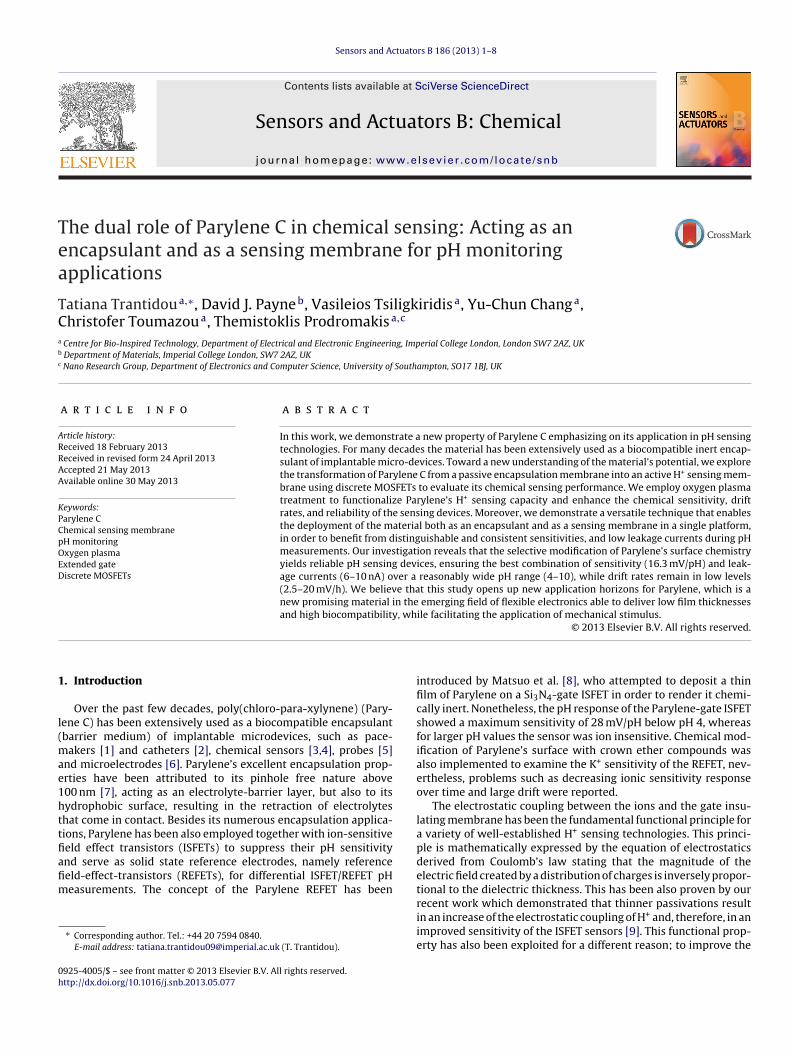
Fig. 1. (a) PCB-based prototype platform with the Au/Parylene sensing sites locatedin the center. (b) Schematic cross section of the fabrication process of untreatedParylene C sensors. (c) Average sensitivity and corresponding measured leakagecurrents over 6 channels of untreated 540 nm, 1 �m and 3 �m thick Parylene C
T. Trantidou et al. / Senso
ensors’ performance, reliability and lifetime by having the activeransducer in a remote location from the chemical sensing site, alsonown as the extended-gate approach [10,11]. A further deploy-ent of this concept was recently demonstrated by our group, inhich discrete metal-oxide-semiconductor FETs (MOSFETs) were
mployed as the active transducers [12]. A set of devices withassive electrodes coated with an insulating membrane (SixNy oriO2) electrostatically couple the electrolyte ions and transduce thevailing chemical potentials to the readout circuitry. The rest ofhe platform is encapsulated with Parylene C to serve as a barrieretween the metal interconnects and the electrolyte providing low
eakage currents.The hydrophobic nature of Parylene C certainly has rendered
he material extremely popular for encapsulation purposes, never-heless, its high biocompatibility and mechanical robustness have
ade the idea of exploiting the material in other applications inter-stingly appealing. Many research efforts have been realized tolter the hydrophobic properties of Parylene C with particular focusn the biomedical applications. Oxygen plasma treatment has beenreviously employed to effectively modify the surface properties ofuch films [13,14], with special emphasis on utilizing the materials a cell culture substrate [15,16]. In other studies, Parylene haseen employed for patterning cells and proteins either by enhanc-
ng attachment of proteins after UV exposure [17], or as a peel-offtencil [18].
In a recent research work, we extrapolated correlations betweenxygen plasma treatment parameters (power intensity, exposureime), hydrophilicity and etching rates, and demonstrated selec-ive hydrophilic patterning for self-alignment applications [19]. Welso established that Parylene tends to partially restore its initialydrophobicity within one week after treatment independently ofhe treatment conditions, nevertheless, restoration saturates to aertain point at which the material is still considered hydrophilic.
In this paper, we aim toward a new understanding of Parylene properties beyond encapsulation, and investigate the material’sotential in H+ sensing. We employ O2 plasma treatment of Pary-
ene in order to improve the chemical sensitivity, drift rates, andeliability of the sensors, and we propose the selective modifica-ion of the polymer’s water surface affinity to utilize the materialoth as an encapsulant as well as a pH sensing membrane, by cre-ting hydrophilic areas that are more sensitive to H+ ions, whileaintaining the desired interfaces hydrophobic to ensure low leak-
ge currents during pH measurements. The work presented hereemonstrates a new functional approach for Parylene C, which cane employed both for in vitro but also for in vivo chemical moni-oring applications.
. Materials and methods
.1. Sensors fabrication
PCB-based platforms (Fig. 1a) consisting of passive Au elec-rodes were thoroughly degreased in acetone, isopropanol (IPA)nd deionized (DI) water, and dehydrated for 60 s at 90 ◦C. Pary-ene C films were deposited by chemical vapor deposition, using
commercially available coater (PDS2010) by vaporizing (150 ◦C)nd then pyrolizing Parylene C dimer (690 ◦C), facilitating three dis-inct thicknesses (540 nm, 1 �m, 3 �m) (Fig. 1b). This set of samplesas used for evaluating pH sensitivity of hydrophobic Parylene C. A
econd group (1 �m, 3 �m) was rendered hydrophilic through oxy-en plasma treatment at 400 W using an ultra high purity plasma
tcher (Nano UHP) at a working pressure of 0.8 mbar. Two dis-inct film thicknesses were derived from the 1 �m-thick sensorsepending on the exposure time-span: (a) a residual thicknessf ∼950 nm, resulting from 1 min-treatment, and (b) a thicknessfilms.
of ∼200 nm resulting from 10 min-treatment. Film thickness wasdetermined through calibration samples where Parylene C wasselectively removed to create a step that was measured by a VeecoDektak Stylus profiler. A third group of 1 �m-thick Parylene C plat-forms was rendered hydrophilic on top of the Au sensing sites only.The fabrication process included the patterning of Parylene C as fol-lows: samples were cleaned and dehydrated as described above.Hexamethyldisilazane (HMDS) was spin-coated on the ParyleneC coated PCBs, succeeded by a 1.4-�m-thick positive photoresist(AZ5214). The samples were then soft-baked on a hotplate at 90 ◦Cfor 60 s, selectively exposed to UV light for 90 s, and developed.Before inserted into the plasma etcher, the samples were prebakedat 110 ◦C for 60 s for hardening the protective photoresist mask.Oxygen plasma treatment was accomplished at 400 W/10 min,facilitating a film thickness of ∼200 nm on top of the electrode sitesonly, whereas hydrophobic Parylene remained intact (1 �m) at therest of the platform. For the fabrication of the patterned matrixthe same procedure was followed with a different mask layout.For thicker Parylene films (3 �m), photoresist AZ4562 (190 s UVexposure, 2 min development time) was utilized instead, due to itsslower etching rate inside the plasma etcher. Plasma treatment wasconducted at 400 W/35 min resulting in a ∼200 nm Parylene thick-
ness on top of the metal sensing sites. After O2 plasma exposure,the photoresist was removed by immersing the platforms into ACE,IPA and then DI water.
rs and
2
otdtdTfptottsstHumEtieetrwm
3
3m
bpAtttmfiamadtwdvtdtacmshdlt
sensors were treated with oxygen plasma at 400 W for 1 and 10 min,resulting in film thicknesses of 950 and 200 nm respectively. Longerexposure to O2 plasma does not only lead to a smaller mem-brane thickness, but also to an increased hydrophilicity. According
T. Trantidou et al. / Senso
.2. Experimental setup
Throughout this study, discrete MOSFETs were employed inrder to evaluate the material’s chemical behavior. An array of p-ype MOSFETs was hosted on an instrumentation system previouslyesigned [12] together with an appropriate multiplexing scheme,he necessary biasing circuitry comprising of dual op-amp source-rain followers, and universal interfacing ports (see Suppl. Fig. 1).o facilitate the transmission of the chemical potentials from theront-end PCB platforms to the read-out circuitry, the fabricatedlatforms were remotely connected with the gates of the MOSFETshrough a connector. The extended-gate approach was selected inur work to improve the sensors’ performance, reliability and life-ime as stated above. Depending on the available ionic resources,he binding of H+ to the membrane surface in the vicinity of theensing sites modulates the gate capacitance that leads to a corre-ponding output (drain) voltage. This in turn changes the MOSFETshreshold voltage and allows straightforward correlations between+ concentration and output voltage. Experiments were performedsing 20 ml of commercial pH buffer solutions (HANNA Instru-ents) with pH values of 4 (HI-7004), 7 (HI-7007) and 10 (HI-7010).
ach sensor was immersed in each electrolyte solution for 2 h forhe drift experiments, and for 200 s for the sensitivity experimentsn the following order: pH 7, 4, 7, 10 and 7. In each case a Ag/AgCllectrode was also immersed in the solution to serve as the refer-nce electrode. Before testing a new electrolyte, the sensors andhe Ag/AgCl electrode were rinsed with DI water to remove anyesidual chemical compounds and wiped carefully. All experimentsere performed at room temperature inside a Faraday cage forinimizing noise.
. Results and discussion
.1. Evaluation of hydrophobic Parylene C as a pH sensingembrane
Chemical sensitivity of the three hydrophobic Parylene mem-ranes (540 nm, 1 �m and 3 �m) was evaluated in solutions ofH 4, 7 and 10 through the ID–VGS curves of the MOSFETs as theg/AgCl reference electrode was swept from −2 to 1 V. Additionally,
he sensors’ transient responses across distinct electrolyte solu-ions were assessed using the instrumentation platform hostinghe active components and the readout circuits (see supplementary
aterial). The output voltage measured is the drain voltage derivedrom the dual op-amp source-drain followers, employed for bias-ng the MOSFETs. Average sensitivities for all three sensor typesre illustrated in Fig. 1c. For each of the three sensing platforms,easurements of the output voltage (mV) over 6 sensing sites were
cquired at pH 4, 7 and 10, and a line was fitted to the experimentalata. The slope (mV/pH) of the fitted line gives the average sensi-ivity of each Parylene sensor. The sensors’ encapsulation qualityas also extrapolated through leakage current measurements con-ucted for ID = 100 �A and VDS = 0.5 V, which are the typical biasingalues defining the operation region of the MOSFETs. In the case ofhe 3 �m thick Parylene membranes, the MOSFETs did not switchuring the voltage sweep, indicating that the material is insensi-ive at ID = 100 �A. Leakage current measurements were conductedt VGS = −0.85 V instead, where the difference between the threeurves is more distinct. The conclusions driven from these experi-ents indicate that Parylene C displays a distinguishable chemical
ensitivity in small film thicknesses (23.97 mV/pH for 540 nm),
owever, the material’s behavior is not always consistent especiallyuring the transition from pH 7 to pH 10. H+ sensitivity becomesower and inconsistent in larger thicknesses (1 �m) and eventuallyhe material preserves its inertness and encapsulation integrity in
Actuators B 186 (2013) 1– 8 3
much higher thicknesses (3 �m). As previously described by Gra-hame [20], the electrolyte–insulator–metal interface results in theformation of a double layer region. A smaller dielectric thicknessbrings the inner Helmholtz layer, i.e. the interfacing H+ ions, closerto the metal surface, introducing a smaller capacitance, which inturn leads to a larger output voltage. Contrary to what is statedin the literature regarding Parylene’s pinhole-free nature above100 nm [7], our experimental data support a pinhole-free behaviorof Parylene at film thicknesses above 1 �m, indicated by a signif-icant decrease in the leakage current as the membrane thicknessincreases from 540 nm to 3 �m. Eventually, a film thickness of 1 �mseems to be a transitional state between pinhole and pinhole-freestatus, also supported by the large standard deviations observed inFig. 1c.
3.2. Evaluation of oxygen plasma treated Parylene C sensors
3.2.1. Conformally O2 plasma treated Parylene CIn order to examine whether an induced hydrophilicity would
enhance Parylene’s pH sensitivity, two sets of 1 �m-thick Parylene
Fig. 2. (a) Representative transient response (non-filtered, non-calibrated data) ofa single sensing site across distinct electrolytes of conformally O2 plasma treated(400 W) 1 �m-thick Parylene sensors exposed for 10 min (top) and 1 min (bottom).(b) Corresponding ID–VGS curves of conformally O2 plasma treated (400 W/10 min)sensor. A schematic cross-section of the fabrication process is also included.

4 T. Trantidou et al. / Sensors and Actuators B 186 (2013) 1– 8
Fig. 3. (a) Cross-section of fabrication process of selectively O2 plasma treated Parylene C sensors. (b) Microscope image of single sensing site rinsed with electrolyte solutionto evaluate selective hydrophilicity. (c) Transient response (non-filtered, non-calibrated data) across distinct electrolytes of selectively O2 plasma treated (400 W/10 min)1 Corred
tttautettFAasvntstueriHfc
3
hleb
�m-thick Parylene sensor 15 days (top) and 45 days (bottom) after treatment. (d)ays and 90 days (subfigure) after treatment.
o our recent findings [19], the water surface affinity of 1 �m-hick untreated and O2 plasma treated Parylene C films (evaluatedhrough static contact angle measurements) corresponds to aver-ge contact angles of 78.85 ± 1.2◦, 4.5 ± 0.8◦ and less than 1◦ forntreated films and films treated (400 W) for 1 and 10 min respec-ively. The plasma treated sensors were tested 15 days after plasmaxposure, so that their induced hydrophilicity stabilizes accordingo previous findings [19]. Fig. 2a presents the transient response ofhe two sensor types when tested with various electrolytes, whileig. 2b reveals the ID–VGS curves of the thin-membrane sensor.s anticipated, the response of the Parylene-coated sensors with
thicker membrane appears noisier and exhibits lower chemicalensitivity comparing to thinner films. To ensure that this obser-ation derives primarily from the smaller residual thickness andot from the extent of the induced hydrophilicity, we conductedhe same experiments (measurements performed over 6 sensingites) with a 3 �m-thick Parylene C sensor that was O2 plasmareated under the same conditions (400 W/10 min), yielding a resid-al thickness of ∼2.1 �m, and confirmed that the sensor did notxhibit any pH sensitivity. It is noteworthy that the improvedesponse of the material is a combination of the degree of thenduced hydrophilicity, and therefore the number of the available
+ binding sites, and the residual thickness, which is a commoneature to all sensing membranes due to Coulomb electrostaticoupling.
.2.2. Selectively O2 plasma treated Parylene CRecently, we demonstrated how to selectively alter the
ydrophobic surface properties of Parylene C through standardithography and oxygen plasma treatment [19]. In this study, wemploy this technique to selectively expose the Parylene mem-rane on top of the gold sensing sites to O2 plasma (400 W/10 min),
sponding ID–VGS curves of selectively O2 plasma treated (400 W/10 min) sensor 45
and benefit from the enhanced pH sensitivity of the inducedhydrophilicity of the Parylene film, while concurrently preservinggood encapsulation integrity of the sensor. A schematic cross-section of the fabrication process is illustrated in Fig. 3a, whileFig. 3b captures the selective hydrophilic patterning of the Parylenefilm which is evaluated by rinsing the whole PCB platform withelectrolyte solution. Selectively treated sensors disclose a highlyreactive behavior when they come in contact with the solutionfor the first time (15 days after O2 plasma exposure). Interest-ingly, their sensing capability appears to stabilize after a few weeks(Fig. 3c). Fig. 3d depicts the ID–VGS curves of selectively treatedsensors tested 45 and 90 days after plasma exposure respectively,indicating that H+ sensitivity is slightly lower in the long-term,nevertheless, it still persists. The induced hydrophilicity of oxy-gen plasma treated Parylene C has been previously attributedto the formation of free carboxyl groups that are prone to bindwith hydrophilic molecules [13,14]. The reactions that take placebetween the hydrophilic groups result in a diminished number offree binding sites on the film surface. As previously showed [19],this phenomenon leads to a partial restoration of the initial Pary-lene C natural hydrophobicity. However, restoration saturates at acertain point within a week after initial exposure to solution, andthe induced hydrophilicity is further sustained.
3.2.3. Comparative characterization of Parylene C sensing devicesFig. 4a summarizes the average pH sensitivities derived from 6
channels of the three 1 �m-thick Parylene sensors (untreated, con-formally and selectively treated at 400 W/10 min). Conformally and
selectively plasma treated sensors exhibit comparable sensitivities(15.5 and 16.3 mV/pH respectively), whereas hydrophobic Parylenedemonstrates a rather low sensitivity of 7.5 mV/pH which is notalways consistent indicated by the large standard deviations. The
T. Trantidou et al. / Sensors and Actuators B 186 (2013) 1– 8 5
F 6 chaP ted Nep
ebawblagcbecsvshtat∼vhhw(p
ig. 4. (a) Chemical sensitivity evaluation of the 1 �m-thick Parylene devices overarylene sensors indicated as the number of experiments in which the sensors exhibierformed over n sensing sites).
ncapsulation properties of the Parylene C sensors were quantifiedy leakage current measurements through the reference electrodet ID = 100 �A (Fig. 4b). The observed sensitivities in all cases areell below the Nerstian [21], nonetheless, the relevant differences
etween the various pH values are still distinguishable, while theeakage current in all cases remains at relatively low levels. It islso worth mentioning that the substantially extended remote-ate employed in this work significantly increases the floating-gateapacitance resulting in a voltage-scaling, which is demonstratedy a lower sensitivity in every case. Results driven from thesexperiments support that the selectively treated Parylene C sensorombines good encapsulation properties and sufficient H+ sen-itivity. The versatility of this method enables us to fabricate aariety of sensors with thicker Parylene membranes to increase theensor’s encapsulation quality, and selectively modify the surfaceydrophobicity by increasing correspondingly the plasma exposureime to get the desired final thickness. For example, we fabricated
3 �m-thick Parylene membrane, which was selectively plasmareated (400 W) for 35 min to obtain a membrane thickness of200 nm on top of the sensing sites (for consistency with the pre-ious experiments), while preserving the thick layer (3 �m) ofydrophobic Parylene on top of the electrode tracks to provide
igh encapsulation quality. The sensor exhibits good sensitivity,hile the measured leakage current remains in very low levels9.8 nA for pH 4, 6.2 nA for pH 7, and 6.1 nA for pH 10), when com-ared against other encapsulants such as epoxies and SU-8 [22].
nnels and (b) corresponding average measured leakage currents. (c) Reliability ofrstian sensitivity out of the total number of experiments conducted (measurements
Previously attained experimental results on SixNy and TiO2 sensingmembranes using the same evaluation methods employed in thiswork [12], demonstrated chemical sensitivities of 35 and 22 mV/pHrespectively which are obviously improved comparing to Parylene;however, these sensing devices suffer from larger leakage currents.Coating these devices with a thick layer of Parylene C (5 �m) pro-vided an improved encapsulation quality with the leakage currentbeing in comparable levels to the results presented here.
The reliability of all Parylene sensors exhibiting H+ sensitivity isestimated in Fig. 4c as the percentage of the experiments in whichthe sensors demonstrated Nerstian sensitivity out of the total num-ber of experiments. Although all four sensors are H+ sensitive, theplasma treated devices reveal a more consistent chemical behavior.
As a proof-of-concept for illustrating Parylene’s capacity to actboth as an encapsulant and as a H+ sensing membrane, we fabri-cated a pattered matrix with the layout presented in Fig. 5a. In thisarrangement Parylene was locally rendered hydrophilic on top ofa group of sensing sites, leaving the other areas hydrophobic. Thesensors were again tested 15 days after treatment for consistencywith the results acquired from previous experiments. Data wereinitially calibrated at pH 7 to remove any offset between the distinctsensing sites and compensate for drift (see supplementary mate-
rial for calibration method). The main purpose of calibration is tomaintain a uniform and relative performance for all sensing sites ofthe array. Fig. 5b illustrates the 3D representation of the calibrateddata obtained from an active area of the matrix consisting of 20
6 T. Trantidou et al. / Sensors and Actuators B 186 (2013) 1– 8
F y the
r ences
ssocse
3
Pdabia
likely to initiate massive reactions between the ions and the freecarboxyl groups present on the surface of treated Parylene, as statedpreviously [13,14].
Table 1Drift rates (mV/h) of Parylene sensors in distinct pH values.a
Parylene C sensors pH 4 pH 7 pH 10
ig. 5. (a) Layout of 1 �m-thick Parylene matrix: hydrophilic areas are indicated besponse of the 20 sensing sites to distinct pH values. (For interpretation of the refer
ensing sites immersed into distinct electrolytes. The hydrophilicites display larger voltage outputs relatively to the hydrophobicnes in all cases, namely a higher sensitivity response to the pHhange. However, due to the interaction between adjacent sensingites, some areas exhibit lower or higher response than normallyxpected.
.3. Chemical drift
Drift experiments were conducted for the three 1 �m-thickarylene sensors for a time period of 2 h. The main source ofrift is attributed to the chemical interaction between the ions
nd the membrane surface, which causes alterations on the mem-rane’s chemical composition and thickness. This drift–pH relations articulated best through an exponential model. Conformallynd selectively plasma exposed (400 W/10 min) Parylene sensors
red circles. (b) Corresponding 3D representation of voltage outputs indicating theto color in this figure legend, the reader is referred to the web version of the article.)
demonstrate lower drift than untreated Parylene, exhibiting thelargest drift rates in pH 4 solution (22.07 and 20.19 mV/h respec-tively), whereas their drift rates for pH 7 and 10 are lower than10 mV/h (Table 1). The large H+ concentration in pH 4 solution is
Untreated 28.93 ± 0.1 16.94 ± 1.9 44.34 ± 0.03Conformally treated (400 W/10 min) 22.07 ± 3.3 2.34 ± 1.5 1.88 ± 1.1Selectively treated (400 W/10 min) 20.19 ± 8.8 9.71 ± 1.9 2.57 ± 3.0
a Average response over 6 channels.

T. Trantidou et al. / Sensors and
Fig. 6. (a) Al K� core level photoemission spectrum of Parylene C in the C 1s region.(a
3
cp1taPaabdlb2lofiOci
References
b) Survey (left column) and C 1s spectra (right column) of (a) untreated Parylene Cnd (b) O2 treated Parylene C (400 W/1 min).
.4. X-ray photoelectron spectroscopy analysis
To understand the effect of oxygen plasma treatment on thehemical sensing performance of Parylene C, we performed X-rayhotoelectron spectroscopy (XPS) measurements on a series of-�m-thick Parylene C films deposited on glass substrates, to inves-igate the composition of the surface chemical bonds before andfter treatment. The C 1s region core-line spectrum of untreatedarylene C is shown in Fig. 6a. At first glance it is apparent that therere two components of the C 1s core line (centered at ∼284.5 eV),nd shake-up satellite structure, due to �–�* excitations on theenzene ring (centered at ∼291.2 eV). Upon peak fitting it can beetermined that the C 1s core line consists of three components
abeled (I, II and III), corresponding to the CH2, aromatic car-on and C Cl chemical environments, at 284.2 eV, 284.6 eV and85.5 eV respectively. There is also a clear signal from the Cl 2p core
evel, and a small amount of oxygen (surface contaminant). Uponxygen plasma treatment (400 W/1 min) it is apparent that the
lms become significantly more oxidized, shown in Fig. 6b, with the1s core level at ∼532.5 eV. The peak at ∼289 eV is most likely fromarboxyl groups (C O), which also agrees well with previous stud-es [13,14]. The sample treated at 400 W/10 min has been greatly
Actuators B 186 (2013) 1– 8 7
functionalized and shows significant surface oxidation (includingthe possibility of pinholes in the film by a concurrent etching pro-cess). The presence of a majority of oxygen species at the Parylenesurface explains the increased hydrophilicity, although to under-stand the oxidation mechanisms fully, this system needs furtherstudy by XPS.
4. Conclusion
In this work, we demonstrate a new property of Parylene Cemphasizing on its application in sensing technologies. Since nowthe material has been primarily used either as a biocompatibleencapsulant of implantable microdevices or as an ion-blockinglayer aiming to suppress chemical sensitivity of the REFET in theISFET/REFET topology. Toward a new understanding of the mate-rial’s potential, we explore the role of Parylene C as an activepH sensing membrane using discrete MOSFETs to evaluate itschemical performance. Clearly, other circuitry, such as instrumen-tation amplifiers, can also be employed as alternative transducingschemes. Contrary to what is stated in the literature, hydropho-bic Parylene seems to exhibit good encapsulation integrity onlyabove 1 �m indicating a pinhole-free behavior, whereas below thisfilm thickness the material displays H+ sensitivity which graduallyincreases for lower film thicknesses, it is not though consistent.Oxygen plasma treatment of Parylene C films was employed to reli-ably enhance the polymer’s pH sensing capacity. Plasma inducedhydrophilicity of Parylene C films yielded significant improve-ment of the H+ sensitivity over the untreated, hydrophobic films(15.5 mV/pH vs. 7.5 mV/pH). In addition, we demonstrate a versa-tile technique to selectively modify the surface hydrophilicity ontop of the sensing sites and increase Parylene’s H+ sensing abil-ity (16.3 mV/pH), while maintaining good encapsulation integritywithin the same sensing platform. The observed sensitivities in allcases appear relatively low, however, this is primarily attributedto the evaluation method employed in this study (extended-gate), which compromises the sensitivity over robustness. Takinginto account Parylene’s high biocompatibility with tissue andbiomolecules, the work presented here paves the way for potentialapplication in 2-D toxicology assays, in which local immobiliza-tion of cells and biomolecules could enable the comprehensiveinterrogation of the cellular metabolism through appropriate mem-brane functionalization. Alternatively, since Parylene can deliverfree-standing ultrathin (down to 1 �m) flexible films, in vivo appli-cation is also feasible based on a more hybrid approach of fabricated“bio-tattoos” performing simultaneously electrical and chemicalmeasurements within the same recording platform. We believethat this study opens up new application horizons for Parylene,which is a new promising material in the emerging field of flexibleelectronics able to deliver low film thicknesses, high biocompati-bility and facilitate the application of mechanical stimulus.
Acknowledgment
The authors would like to acknowledge the financial support ofthe A.G. Leventis Foundation.
Appendix A. Supplementary data
Supplementary data associated with this article can be found, inthe online version, at http://dx.doi.org/10.1016/j.snb.2013.05.077.
[1] N. Iguchi, H. Kasanuki, N. Matsuda, M. Shoda, S. Ohnishi, S. Hosoda, Contact sen-sitivity to polychloroparaxylene-coated cardiac pacemaker, Pacing and ClinicalElectrophysiology 20 (1997) 372.

8 rs and
[
[
[
[
[
[
[
[
[
[
[
[
[
B
Ti
T. Trantidou et al. / Senso
[2] L. Wolgemuth, Crystal-clear coating covers components, Medical Design 6(2006) 48–51.
[3] T. Prodromakis, K. Michelakis, T. Zoumpoulidis, R. Dekker, C.C. Toumazou,Biocompatible encapsulation of CMOS based chemical sensor, IEEE SensorsConference (2009) 791.
[4] X. Liu, L. Li, B. Awate, R.M. Worden, G. Reguera, A.J. Mason, Biosensor arraymicrosystem on a CMOS amperometric readout chip, IEEE Biomedical Circuitsand Systems Conference (2011) 305.
[5] S. Takeuchi, D. Ziegler, Y. Yoshida, K. Mabuchi, T. Suzuki, Parylene flexible neuralprobes integrated with microfluidic channels, Lab on a Chip 5 (2005) 519.
[6] E.M. Schmidt, M.J. Bak, P. Christensen, Laser exposure of Parylene-C insulatedmicroelectrodes, Journal of Neuroscience Methods 62 (1995) 89.
[7] SCS Medical Coatings, Specialty Coating Systems, Indianapolis, Indiana.Available from: http://scscoatings.com/corporate/library.aspx (last accessed18.04.13).
[8] T. Matsuo, H. Nakajima, T. Osa, J. Anzai, Parylene-gate ISFET and chemical mod-ification of its surface with crown ether compounds, Sensors and Actuators 9(1986) 115.
[9] T. Prodromakis, Y. Liu, T. Constandinou, P. Georgiou, C. Toumazou, ExploitingCMOS technology to enhance the performance of ISFET sensors, IEEE ElectronDevice Letters 31 (2010) 1053.
10] L.-T. Yin, J.-C. Chou, W.-Y. Chung, T.-P. Sun, S.-K. Hsiung, Separate structureextended gate H+-ion sensitive field effect transistor on a glass substrate, Sen-sors and Actuators B: Chemical 71 (2000) 106.
11] C.-G. Ahn, A. Kim, C.W. Park, C.S. Ah, J.-H. Yang, T.-Y. Kim, M. Jang, G.Y. Sung,Modified ion sensitive field effect transistor sensors having an extended gateon a thick dielectric, Applied Physics Letters 96 (2010) 203702.
12] T. Prodromakis, Y. Liu, J. Yang, D. Hollinghurst, C. Toumazou, A novel designapproach for developing chemical sensing platforms using inexpensive tech-nologies, IEEE Biomedical Circuits and Systems Conference (2011) 369.
13] J.W. Seong, K.W. Kim, Y.W. Beag, S.K. Koh, K.H. Yoon, J.H. Lee, Effects of ion bom-bardment with reactive gas environment on adhesion of Au films to ParyleneC film, Thin Solid Films 476 (2005) 386.
14] J.S. Song, S. Lee, S.H. Jung, G.C. Cha, M.S. Mun, Improved biocompatibility ofparylene-C films prepared by chemical vapour deposition and the subsequentplasma treatment, Journal of Applied Polymer Science 112 (2008) 3677.
15] T.Y. Chang, V.G. Yadav, S. De Leo, et al., Cell and protein compatibility ofparylene-C surfaces, Langmuir 23 (2007) 11718.
16] T. Hoshino, I. Saito, R. Kometani, et al., Improvement of neuronal cell adhe-siveness on parylene with oxygen plasma treatment, Journal of Bioscience andBioengineering 113 (2011) 395.
17] E. Delivopoulos, A.F. Murray, J.C. Curtis, Effects of parylene-C photooxidation onserum-assisted glial and neuronal patterning, Journal of Biomedical MaterialsResearch 94 (2010) 47.
18] C.P. Tan, B.R. Cipriany, D.M. Lin, H.G. Craighead, Nanoscale resolution, multi-component biomolecular arrays generated by aligned printing with parylenepeel-off, NanoLetters 10 (2010) 719.
19] T. Trantidou, T. Prodromakis, C. Toumazou, Oxygen plasma inducedhydrophilicity of Parylene-C thin films, Applied Surface Science 261 (2012) 43.
20] D.C. Grahame, The electrical double layer and the theory of electrocapillarity,Chemical Reviews 41 (1947) 441.
21] L. Bousse, The chemical sensitivity of electrolyte/insulator/siliconstructures—fundamentals of ISFET operation, Technische Hogeschool,Delft, The Netherlands, 1982 (Ph.D. dissertation).
22] T. Prodromakis, P. Georgiou, T.G. Constandinou, et al., Batch encapsulation tech-nique for CMOS based chemical sensors, IEEE Biomedical Circuits and SystemsConference (2008) 321.
iographies
atiana Trantidou received her M.Eng. degree in Electrical & Computer Engineer-ng in 2009 from the Aristotle University of Thessaloniki, Greece and her M.Sc.
Actuators B 186 (2013) 1– 8
degree in Biomedical Engineering from Imperial College London, UK in 2010. Sheis currently pursuing a Ph.D. in bio-inspired devices under the supervision of DrT. Prodromakis and Prof. C. Toumazou at the Department of Electrical & ElectronicEngineering at Imperial College London, UK. Her interests are in biomedical devicesand point-of-care applications, while she already holds a patent in the field. Herarea of research is currently being focused on the micro-fabrication of advanced cellculturing platforms with application in next-generation toxicology assays.
David J. Payne received his M.Chem. (2004) from Cardiff University and D.Phil.(2008), in Experimental Solid-State Chemistry, from the University of Oxford, UK.From 2007 he was a Junior Research Fellow at Christ Church, University of Oxford.His research focuses on the spectroscopic determination of the electronic structureof oxide materials, and in particular developing (lab-based) near-ambient pressureX-ray photoelectron spectroscopy (NAP-XPS). His interests are in oxide materialsfor energy applications including solar water splitting, photovoltaics and transpar-ent conducting oxides. In 2011 he was appointed as a lecturer in the Department ofMaterials at Imperial College London.
Vasileios Tsiligkiridis received the diploma degree in Electrical and ComputerEngineering in 2011 from the University of Patras, Greece and the M.Sc. degreein Biomedical Engineering in 2012 from Imperial College London, UK. Hisresearch interests include point-of-care medical diagnostics/monitoring solutions,biosensors and biomedical signal processing, with a particular interest in neuroapplications.
Yu-Chun Chang received a bachelor’s degree in Mechatronics Engineering in 2010from the University of Cape Town, South Africa. He obtained his M.Sc. in ControlSystems Engineering in 2012 from Imperial College London, UK. He is currentlypursuing a Ph.D. degree in Neural & Behavioral Sciences at the Max Planck Insti-tute for Biological Cybernetics in cooperation with the University of Tübingen. Hisresearch interests include instrumentation, control systems and image processingfor medical applications with a particular interest in magnetic resonance imaging.
Christofer Toumazou is a professor of Circuit Design, Founder and Executive Direc-tor of the Institute of Biomedical Engineering at Imperial College London, UK. Prof.Toumazou has made outstanding contributions to the fields of low power analogcircuit design and current mode circuits and systems for biomedical and wirelessapplications. Through his extensive record of research, he has invented innova-tive electronic devices ranging from dual mode cellular phones to ultra-low powerdevices for both medical diagnosis and therapy. He has published over 320 researchpapers in the field of RF and low power electronics and is a member of many pro-fessional committees. He holds 23 patents in the field, many of which are now fullygranted PCT. He is the founder of four technology based companies with applica-tions spanning ultra low-power mobile technology and wireless vital sign monitors(Toumaz Technology Ltd., UK), biomedical devices (Applied Bionics PTE, Singapore),digital audio broadcasting (FutureWaves Pte Taiwan) and DNA detection (DNAElectronics Ltd., UK). These companies employ over 50 RF/low power engineersworldwide many of who are Professor Toumazou’s ex-graduate students. ProfessorToumazou was invited to deliver the 2003 Royal Society Clifford Patterson Prize Lec-ture, entitled “The Bionic Man”, for which he was awarded The Royal Society CliffordPatterson bronze medal. He was recently awarded the IEEE CAS Society EducationAward for pioneering contributions to telecommunications and biomedical circuitsand systems, and the Silver Medal from the Royal Academy of Engineering for hisoutstanding personal contributions to British engineering. In 2008, he was electedto the grade of Fellow of both the Royal Society and Royal Academy of Engineering.
Themistoklis Prodromakis is a reader in Nanoelectronics within the Nano ResearchGroup, ECS department at University of Southampton. He previously held a CorriganFellowship in Nanoscale Technology and Science, funded by the Corrigan Founda-tion and LSI Inc., within the Centre for Bio-inspired Technology at Imperial College
London and a Lindemann Trust Visiting Fellowship in EECS UC Berkeley. Dr. Prodro-makis is a member of the IEEE, the INE and the IET, and also serves as member of theBioCAS Technical Committee of the IEEE Circuits & Systems Society. His backgroundis in electron devices and micro/nano-electronics processing techniques, with hisresearch being focused on bio-inspired devices for biomedical applications.