
Semiconductor Business Presentation - Sony · Semiconductor Business Presentation Agenda 1. FY2007...
14
1 Semiconductor Business Semiconductor Business Presentation Presentation Sony Corporation Sony Corporation Executive Deputy President Executive Deputy President Corporate Executive Officer Corporate Executive Officer President of the Semiconductor President of the Semiconductor Business Group Business Group Yutaka Nakagawa Yutaka Nakagawa Feb. 21 Feb. 21 st st , 2008 , 2008 ( ( Thu. Thu. ) ) Sony Semiconductor Business Group Organization Sony Semiconductor Business Group Organization Semiconductor Semiconductor Business Group Business Group Image Sensor Business Division Image Sensor Business Division Micro Device Business Division Micro Device Business Division LSI Business Division LSI Business Division Laser Business Division Laser Business Division Sony Semiconductor Kyushu Corp. Sony Semiconductor Kyushu Corp. Sony Shiroishi Semiconductor Inc. Sony Shiroishi Semiconductor Inc. Design Platform Division Design Platform Division Semiconductor Technology Semiconductor Technology Development Division Development Division Research & Development Division Research & Development Division Semiconductor Sales Division Semiconductor Sales Division Planning & Control Division Planning & Control Division Quality Assurance Division Quality Assurance Division Sony LSI Design Inc. Sony LSI Design Inc. DP T.Saito DP T. Suzuki DP M. Tsuruta President Y. Nakagawa Senior General Manager Senior General Manager T. Ogasawara T. Ogasawara Senior General Manager Senior General Manager Y.Osa Y.Osa Senior General Manager Senior General Manager T. Saito T. Saito Senior General Manager Senior General Manager Y. Ueda Y. Ueda Senior General Manager Senior General Manager S.Hashimoto S.Hashimoto Senior General Manager Senior General Manager M. M. Tsuruta Tsuruta Senior General Manager Senior General Manager T.Kusuda T.Kusuda Senior General Manager Senior General Manager S. Iwase S. Iwase Senior General Manager Senior General Manager Y. Okamoto Y. Okamoto Senior General Manager Senior General Manager N. N. Shirota Shirota President S.Tanemo President N. Shirota President H.Sudou
Transcript of Semiconductor Business Presentation - Sony · Semiconductor Business Presentation Agenda 1. FY2007...

1
Semiconductor Business Semiconductor Business PresentationPresentation
Sony CorporationSony CorporationExecutive Deputy PresidentExecutive Deputy PresidentCorporate Executive OfficerCorporate Executive Officer
President of the Semiconductor President of the Semiconductor Business GroupBusiness Group
Yutaka NakagawaYutaka Nakagawa
Feb. 21Feb. 21stst, 2008 , 2008 ((Thu.Thu.))
Sony Semiconductor Business Group OrganizationSony Semiconductor Business Group Organization
Semiconductor Semiconductor Business GroupBusiness Group
Image Sensor Business DivisionImage Sensor Business Division
Micro Device Business Division Micro Device Business Division
LSI Business DivisionLSI Business Division
Laser Business DivisionLaser Business Division
Sony Semiconductor Kyushu Corp. Sony Semiconductor Kyushu Corp.
Sony Shiroishi Semiconductor Inc.Sony Shiroishi Semiconductor Inc.
Design Platform DivisionDesign Platform Division
Semiconductor Technology Semiconductor Technology Development DivisionDevelopment Division
Research & Development DivisionResearch & Development Division
Semiconductor Sales DivisionSemiconductor Sales Division
Planning & Control DivisionPlanning & Control Division
Quality Assurance DivisionQuality Assurance Division
Sony LSI Design Inc.Sony LSI Design Inc.
DP T.SaitoDP T. SuzukiDP M. Tsuruta
President Y. Nakagawa
Senior General Manager Senior General Manager T. OgasawaraT. Ogasawara
Senior General Manager Senior General Manager Y.OsaY.Osa
Senior General Manager Senior General Manager T. SaitoT. Saito
Senior General Manager Senior General Manager Y. UedaY. Ueda
Senior General Manager Senior General Manager S.HashimotoS.Hashimoto
Senior General Manager Senior General Manager M. M. TsurutaTsuruta
Senior General Manager Senior General Manager T.KusudaT.Kusuda
Senior General Manager Senior General Manager S. IwaseS. Iwase
Senior General Manager Senior General Manager Y. OkamotoY. Okamoto
Senior General Manager Senior General Manager N. N. ShirotaShirota
President S.Tanemo
President N. Shirota
President H.Sudou

2
Semiconductor Business Presentation
AgendaAgenda
1. FY2007 Review ⅰ)Initiatives
・Asset Light ・Selection & Focus
ⅱ)Key Performance Indicators
2. For FY2008
Semiconductor Business Presentation
AgendaAgenda
1. FY2007 Review ⅰ)Initiatives
・Asset Light ・Selection & Focus
ⅱ)Key Performance Indicators
2. For FY2008

3
Semiconductor Business Presentation
■ Background of Asset Light
Lack of applications (technology drivers)for cutting-edge line → Failure of “Water Fall Strategy”
■ Purpose of Asset LightDevelop flexible cutting-edge MOS Logic production depending on volume due to the effective utilization of alliances/foundries with other companies(Bear all fixed costs → bear variable costs)
※In-house production of image sensors, etc. for high value-added process development /manufacturing technology
Asset LightAsset Light
NagasakiNagasakiOTSSOTSS
FishkillFishkill
Increase chip outputIncrease chip outputwith shift to next with shift to next generation process generation process
(Assuming constant monthly wafer unit production)
Image of possible “PS3” Core LSIunit production
90nm 65nm 45nm
Semiconductor Business Presentation
Asset LightAsset Light
Sony Nagasaki Fab2 Change from inChange from in--house production to foundry procurementhouse production to foundry procurement ・ ・Sale of FacilitiesSale of Facilities ・ ・Establishment of a new JV companyEstablishment of a new JV company
Oita TSSemiconductor Corp. (OTSS)
Change from inChange from in--house production to foundry procurementhouse production to foundry procurement ・ ・Termination of JV contractTermination of JV contract ・ ・Sale of FacilitiesSale of Facilities
IBM East Fishkill Factory Change from inChange from in--house production to foundry procurement ofhouse production to foundry procurement of
45nm45nm““Cell/B.E.Cell/B.E.””
Cutting-edge process development
(IBM, Sony, Toshiba)
Early withdrawal from joint development agreement for cuttingEarly withdrawal from joint development agreement for cutting--edge process technologies at 32nm and beyond edge process technologies at 32nm and beyond ((Ended Dec. 21, 2007Ended Dec. 21, 2007))
(“Cell/B.E.” “RSX” Production)
(“RSX” Production)
(“Cell/B.E.” Production)※
※
※
“Cell Broadband Engine™”=“Cell/B.E.”
4
Semiconductor Business Presentation
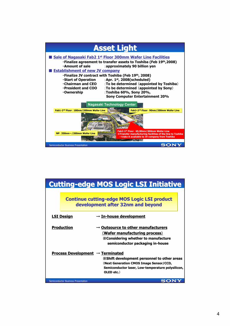
Asset LightAsset Light■ Sale of Nagasaki Fab2 1st Floor 300mm Wafer Line Facilities
・Finalize agreement to transfer assets to Toshiba (Feb 19th,2008)・Amount of sale :approximately 90 billion yen
■ Establishment of new JV company・Finalize JV contract with Toshiba (Feb 19th, 2008)・Start of Operation :Apr. 1st, 2008(scheduled)
・Chairman and CEO :To be determined (appointed by Toshiba)・President and COO :To be determined (appointed by Sony)・Ownership :Toshiba 60%, Sony 20%,
Sony Computer Entertainment 20%
Fab2-2nd Floor: 90nm/200mm Wafer Line
NP: 350nm~/200mm Wafer Line Fab2-1st Floor: 65,90nm/300mm Wafer Line※Transfer manufacturing facilities of the line to Toshiba →Make it available to JV company from Toshiba
Fab1-2nd Floor: 180nm/200mm Wafer Line
Nagasaki Technology Center
Semiconductor Business Presentation
CuttingCutting--edge MOS Logic LSI Initiativeedge MOS Logic LSI Initiative
Continue cuttingContinue cutting--edge MOS Logic LSI product edge MOS Logic LSI product development after 32nm and beyonddevelopment after 32nm and beyond
LSI DesignLSI Design → → InIn--house developmenthouse development
ProductionProduction → → Outsource to other manufacturersOutsource to other manufacturers ((Wafer manufacturing processWafer manufacturing process)) ※ ※Considering whether to manufacture Considering whether to manufacture semiconductor packaging insemiconductor packaging in--househouse
Process DevelopmentProcess Development → → TerminatedTerminated ※ ※Shift development personnel to other areasShift development personnel to other areas ((Next Generation CMOS Image Sensor/CCD,Next Generation CMOS Image Sensor/CCD, Semiconductor laser, LowSemiconductor laser, Low--temperature temperature polysiliconpolysilicon,, OLED etc.OLED etc.))

5
Semiconductor Business Presentation
FY05 FY06 FY07
CuttingCutting--edge Image Sensor Developmentedge Image Sensor Development
1.41.4um CMOS Image Sensorum CMOS Image Sensor/image sensing for cellular/image sensing for cellular
System on Chip DevelopmentSystem on Chip Development
Lead industry for product Lead industry for product shipment timeshipment time
Realize high image quality Realize high image quality
3535mm fullmm full--sizesizeCMOS Image Sensor CMOS Image Sensor
development for Ddevelopment for D--SLRSLR
Realize high yield Realize high yield and high image qualityand high image quality
Technology fostered with leading Technology fostered with leading process development and productionprocess development and production
Technology for: Technology for: Microfabrication/3D simulation/Microfabrication/3D simulation/
Yield improvement/NoiseYield improvement/Noise--reductionreduction etc.etc.
Image of the trend of Image of the trend of Sony semiconductor R&D Sony semiconductor R&D
expensesexpenses(R&D, D&D)(R&D, D&D)
Without increasing total R&D expenses, strengthen and shift power to image sensor
Without increasing total R&D expenses, strengthen and shift power to image sensor
ImageImageSensorSensor
Semiconductor Business Presentation
AgendaAgenda
1. FY2007 Review ⅰ)Initiatives
・Asset Light ・Selection & Focus
ⅱ)Key Performance Indicators
2. For FY2008

6
Semiconductor Business Presentation
Selection and Focus: Selection and Focus: Initiatives in Business Focus AreasInitiatives in Business Focus Areas
TV/Video
・・Full entryFull entry into LCD Source Drivers LCD Source Drivers ((10bit/8bit10bit/8bit))・・Silicon Tuner Chip set commercializationSilicon Tuner Chip set commercialization・・Commence 2nd Generation Commence 2nd Generation BluBlu--rayray Chip set mass Chip set mass production shipmentsproduction shipments
Game
・・Commence 65nm Commence 65nm ““Cell/B.E.Cell/B.E.”” mass production shipmentsmass production shipments((11stst Half of FY07Half of FY07))
・・Commence 65nm Commence 65nm ““RSXRSX”” mass production shipmentsmass production shipments((22ndnd Half of FY07Half of FY07))
・・Commence LSI mass production shipments for the newCommence LSI mass production shipments for the newmodel model ““PSPPSP”” (Release Date Sep. 2007)(Release Date Sep. 2007)
ImageSensor
・・High S/N highHigh S/N high--speed A/Dspeed A/D--equipped CMOS Image Sensor equipped CMOS Image Sensor Expansion of Expansion of ““ExmorExmor””
APSAPS--C size C size 112 mega pixels for D2 mega pixels for D--SLRSLR 1.75um 1/3.2 type 5 mega pixels for cellular1.75um 1/3.2 type 5 mega pixels for cellular 1.77um 1/3.1 type 5 mega pixels for camcorders etc 1.77um 1/3.1 type 5 mega pixels for camcorders etc ・・Image Sensor cumulative shipments: Image Sensor cumulative shipments: Achieved Achieved 8800 million units 00 million units ((as of Dec. 2007as of Dec. 2007))
・・5 mega pixels and over5 mega pixels and over--equipped sensor share for cellular:equipped sensor share for cellular: Attained about 75% share Attained about 75% share ((Sony estimateSony estimate))““αα770000””
““CyberCyber--shotshotCell phoneCell phone”” ““HDRHDR--SR11/12SR11/12””
Semiconductor Business Presentation
Selection and FocusSelection and Focus
Power ShiftPower Shift
GameGame
TV/VideoTV/Video
Digital ImagingDigital Imaging
Analog ICAnalog IC
etc.etc.
CCDCCD
CMOSCMOSImage SensorImage Sensor
Image sensingImage sensingSystem on ChipSystem on Chip
etc.etc.
Power ShiftPower Shift
System LSISystem LSI Image SensorImage Sensor
Focus Categories
Focus Focus CategoriesCategories
Sele
ctio
n C
ateg
orie
sSe
lect
ion
Cat
egor
ies
Sele
ctio
n C
ateg
orie
s
Focus Categories
Focus Focus CategoriesCategories
7
Semiconductor Business Presentation
AgendaAgenda
1. FY2007 Review ⅰ)Initiatives
・Asset Light ・Selection & Focus
ⅱ)Key Performance Indicators
2. For FY2008
Semiconductor Business Presentation
-2,000
0
2,000
4,000
6,000
8,000
10,000
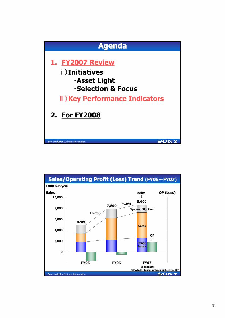
Sales/Operating Profit (Loss) Trend Sales/Operating Profit (Loss) Trend ((FY0FY055~~FY0FY07)7)
4,960
7,8008,600
(’000 mln yen)
(Forecast)
+59%
+10%
ImageImageSensorSensor
GameGame
System LSI, otherSystem LSI, other
FY05 FY06 FY07
Sales↓
OP↓
SalesSales OP (Loss)OP (Loss)
※Excludes Laser, includes high-temp. LCD

8
Semiconductor Business Presentation
0
400
800
1,200
1,600
FY04 FY05 FY06 FY07
Capital Expenditure Trend Capital Expenditure Trend ((FY04FY04~~FY07FY07))
(’000 mln yen)
(Forecast)
1,5001,400
1,500
1,100
ImageImageSensorSensor
GameGame
System LSI, OtherSystem LSI, Other
<Direction>Reduce investment in MOS,active investment in ImageSensor
<Direction>Reduce investment in MOS,active investment in ImageSensor
Semiconductor Business Presentation
AgendaAgenda
1. FY2007 Review ⅰ)Initiatives
・Asset Light ・Selection & Focus
ⅱ)Key Performance Indicators
2. For FY2008

9
Semiconductor Business Presentation
Business PoliciesBusiness Policies
■■ Continuation/Strengthening of Continuation/Strengthening of Selection and FocusSelection and Focus
■■ Continued profit generation structureContinued profit generation structure
Semiconductor Business Presentation
Image SensorImage Sensor BusinessBusiness
■ Strengthen production capacity (June 6th, 2007 announcement)Increase floor space of clean room in Building No.2 ,Kumamoto Tech by 5,000㎡Expand production facilities
■ Take advantage of Sony’s technological edge, maintain CCD business
■ Expand D-SLR business due to mass production of 35mm full-sizeCMOS image sensors
(Jan. 30th, 2008 announcement)
Maintain share, expand market in Maintain share, expand market in ““LargeLarge--sizesize”” ““High image quality High image quality /High resolution/High resolution”” Areas Areas
Share expansion in the Volume Zone for CellularShare expansion in the Volume Zone for Cellular
・35mm full-size 24.81 effective mega pixels
・ High S/N・high speed imaging ~All-pixel scan mode 6.3 frames/s~
αflagship model

10
Semiconductor Business Presentation
Key Factors for Cellular BusinessKey Factors for Cellular Business
1.41.4um CMOS Image Sensorum CMOS Image SensorLead industry for mass productionLead industry for mass production
1.4um1.4um image sensingimage sensingSystem on ChipSystem on Chip mass mass
production commencedproduction commenced
1.4um/8 mega pixels Imageby Prototype CMOS
1.4um Pixel Low Noise Process
Compact & High Performance ISP
Column ADC for High Speed & Low Noise
Compact Size &Best Picture Quality
0
20
69
40
60
80
2007 2008
Mpcs
21
16
Sony volumeexceeds 300% compared to the prior year
50
Volume of Sensors for cell phones equipped with CMOS exceeding 5 mega pixels
(about 72%)
(about 75%)
(Sony Share)
※Imaging Signal Processor
※
~Survey by Sony~
Mkt.Sony
Share Target FY2009 12%Share Target FY2009 12%
HighHigh--end (5 mega pixels and overend (5 mega pixels and over)) Affordable Range (3 mega pixel rangeAffordable Range (3 mega pixel range))
Semiconductor Business Presentation
Contribute to SonyContribute to Sony’’s Game business with active s Game business with active cost reduction of the cost reduction of the ““PS3PS3”” Core LSICore LSI
GameGame--related Businessrelated Business
■ Flexible production by using the new JV company, Toshiba, IBM, and other foundries ■ Continuous improvement of quality and yield of the “PS3” Core LSI 65nm generation
■ Initiatives to develop the next generation shrink versions -Full launch of the development and design of the 45nm “PS3” Core LSI -Continuous improvement and development of LSI for “PSP”
Image of the cost trend for the “PS3” Core LSI
90nm 65nm 45nm

11
Semiconductor Business Presentation
System LSI Business System LSI Business ((TV, Video, Digital ImagingTV, Video, Digital Imaging))
Silicon Tuner Chip setSilicon Tuner Chip setFront End LSIFront End LSIBack End LSI etc.Back End LSI etc.
BluBlu--ray Chip Setray Chip Setetc.etc.
AV CodecAV CodecIImage processing enginemage processing engineetc.etc.
Strengthen cooperation with Sony inStrengthen cooperation with Sony in--house set business unitshouse set business units
Take advantage of Take advantage of semiconductor ksemiconductor knownow--hhowow,,From a From a ““vertical integration structurevertical integration structure””
to an to an ““technology solution service structuretechnology solution service structure”” businessbusiness
Architecture/Algorithm design
RTL design
Layout/Mask design
Wafer production
Test (PC)
Assembly/PackagingTest (FC)
Architecture/Algorithm design
RTL design
Layout/Mask design
Wafer production
Test (PC)
Assembly/Packaging
Test (FC)
Design for TestabilityDesign for Testability
Design for ManufacturingDesign for Manufacturing
Semi Packaging Tech Semi Packaging Tech ((SiPSiP etcetc))
CodesignCodesign/Verification/Verification
BuiltBuilt--in Selfin Self--TestingTesting
BuiltBuilt--on Selfon Self--TestingTesting
Semiconductor Business Presentation
Technology Solution Service Technology Solution Service ((Semiconductor PackagingSemiconductor Packaging))
Offer a total solution with SonyOffer a total solution with Sony’’s cuttings cutting--edge edge SiPSiP technologytechnology
ProductProduct Package structurePackage structure
MobileMobile
DSC/DVCDSC/DVC
Mobile PhoneMobile Phone
GameGame
“PS3”
PoP(Package on Package)
PiP(Package in Package)
MCP(Multi Chip Package)
FC-BGA(Flip Chip BGA)
FC-BGA(Flip Chip BGA)
PBGA(Plastic BGA)
“PS2”
“PSP”

12
Semiconductor Business Presentation
Analog BusinessAnalog BusinessBusiness development focused on categoriesBusiness development focused on categories
where Sony has competitive strengthwhere Sony has competitive strength((LCD LCD Source DriverSource Driver, , PDICPDIC, , I/F ICI/F IC, Power , Power ICIC, , MMICMMIC))
LCD TVs are equipped withan average of about 10 LCD source drivers
■■Take advantage of SonyTake advantage of Sony’’s technological edge in 10bit/Multis technological edge in 10bit/Multi--ChannelChannel、、 Improve the ratio of inImprove the ratio of in--house large screen LCD TVs equipped withhouse large screen LCD TVs equipped with
Sony LCD Source DriversSony LCD Source Drivers■■Expand external salesExpand external sales
6.3
10.0
(Forecast)
Start shipping Full entry Business Expansion
FY06 FY07 FY08~
(mln units)
LCD SourceDriver Biz.
Image of Sony LCD TV unit shipment trend
< LCD Source Driver >
Semiconductor Business Presentation
Semiconductor Laser BusinessSemiconductor Laser Business
■ Maintain No.1 share of blue-violet laser market for playback and recordingFY2007 blue-violet laser market share 74% (Sony estimate)
■ Mass production of blue-violet optical-integrated device by year-end(Jan. 30, 2008 announcement)
■ Cumulative unit shipments of semiconductor laser diodes:Achieved 2.25 billion units (At the end of Jan. 2008)
Active development of the blueActive development of the blue--violet laser violet laser for for BluBlu--rayray
Blue-violet semiconductor laser for Blu-ray H/H Drives 5.6mmφpackage Slim Drives 3.8mmφpackage
Optical-integrated device for Blu-ray Basic prototype (14mm X 7.4mm X 3mm)
Joint development with Nichia Corp.

13
Semiconductor Business Presentation
Production SitesProduction Sites
Nagasaki TECNagasaki TEC((MOS production siteMOS production site))
Kagoshima TECKagoshima TEC((MultiMulti--category production sitecategory production site))
Oita TECOita TEC((CuttingCutting--edge packagingedge packaging
development /production sitedevelopment /production site))
Kumamoto TECKumamoto TEC((Imaging device production siteImaging device production site))
Sony Device TechnologySony Device Technology(Thailand) Co., Ltd.(Thailand) Co., Ltd.
((Assembly siteAssembly site))
Sony Shiroishi Semiconductor Inc.Sony Shiroishi Semiconductor Inc.((Semiconductor laser production siteSemiconductor laser production site))
Sony Semiconductor Kyushu Corp.Sony Semiconductor Kyushu Corp.
Semiconductor Business Presentation
Sony Semiconductor BusinessSony Semiconductor Business
Advantage of having a significant in-house set business(TV, Video, Digital Imaging, Game, etc.)
Technological strength of Sony Semiconductor(Image Sensor, LSI for Game, etc.)

14
Semiconductor Business Presentation


![[4Q FY2007 : 2008년1월~ 2008년3월] 대우증권4Q FY2007 …€¦ · [4Q FY2007 : 2008년1월~ 2008년3월] 대우증권4Q FY2007 실적 ... EastlionWorldwide’의해외교환사채(EB)](https://static.fdocuments.net/doc/165x107/5f0546797e708231d41227d4/4q-fy2007-2008e1-2008e3-eoeeoe4q-fy2007-4q-fy2007-2008e1.jpg)
