SAR ADC’s vs. Delta Sigma ADC’s - TI Training 10101010101010 10101010111010 01010011101101...
56
11001101011010 10101010101010 10101010111010 01010011101101 010101 SAR ADC’s vs. Delta-Sigma ADC’s: Different Architectures for Different Applications 1
Transcript of SAR ADC’s vs. Delta Sigma ADC’s - TI Training 10101010101010 10101010111010 01010011101101...

11001101011010
10101010101010
10101010111010
01010011101101
010101
SAR ADC’s vs. Delta-Sigma ADC’s: Different Architectures for Different Applications
1
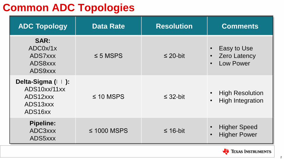
Common ADC Topologies
ADC Topology Data Rate Resolution Comments
SAR:
ADC0x/1x
ADS7xxx
ADS8xxx
ADS9xxx
≤ 5 MSPS ≤ 20-bit
• Easy to Use
• Zero Latency
• Low Power
Delta-Sigma ( ):
ADS10xx/11xx
ADS12xxx
ADS13xxx
ADS16xx
≤ 10 MSPS ≤ 32-bit • High Resolution
• High Integration
Pipeline:
ADC3xxx
ADS5xxx
≤ 1000 MSPS ≤ 16-bit • Higher Speed
• Higher Power
2

ADC Topology Data Rate Resolution Comments
SAR:
ADC0x/1x
ADS7xxx
ADS8xxx
ADS9xxx
≤ 5 MSPS ≤ 20-bit
• Easy to Use
• Zero Latency
• Low Power
Delta-Sigma ( ):
ADS10xx/11xx
ADS12xxx
ADS13xxx
ADS16xx
≤ 10 MSPS ≤ 32-bit • High Resolution
• High Integration
Pipeline:
ADC3xxx
ADS5xxx
≤ 1000 MSPS ≤ 16-bit • Higher Speed
• Higher Power
Common ADC Topologies
3

Common ADC Topologies
Pipeline
SAR
24
20
16
12
8
32
1K 100 10 10K 100K 1M 10M 100M 1G
Co
nve
rte
r R
es
olu
tio
n (
bit
s)
Conversion Rate (SPS)
~ ~
Advantages • Low Latency-time
• High Accuracy
• Typically Low Power
• Easy to Use
Disadvantages • Max FSAMP of 2-5Mhz
SAR Architecture
Delta-Sigma
4

ADC Topology Data Rate Resolution Comments
SAR:
ADC0x/1x
ADS7xxx
ADS8xxx
ADS9xxx
≤ 5 MSPS ≤ 20-bit
• Easy to Use
• Zero Latency
• Low Power
Delta-Sigma ( ):
ADS10xx/11xx
ADS12xxx
ADS13xxx
ADS16xx
≤ 10 MSPS ≤ 32-bit • High Resolution
• High Integration
Pipeline:
ADC3xxx
ADS5xxx
≤ 1000 MSPS ≤ 16-bit • Higher Speed
• Higher Power
Common ADC Topologies
5

Common ADC Topologies
Pipeline
SAR
24
20
16
12
8
32
1K 100 10 10K 100K 1M 10M 100M 1G
Co
nve
rte
r R
es
olu
tio
n (
bit
s)
Conversion Rate (SPS)
Delta-Sigma Architecture
Advantages • High Resolution
• Low Noise
• High Stability
• High Integration
Disadvantages • Cycle-Latency
Delta-Sigma
~ ~
6

ADC Topology Data Rate Resolution Comments
SAR:
ADC0x/1x
ADS7xxx
ADS8xxx
ADS9xxx
≤ 5 MSPS ≤ 20-bit
• Easy to Use
• Zero Latency
• Low Power
Delta-Sigma ( ):
ADS10xx/11xx
ADS12xxx
ADS13xxx
ADS16xx
≤ 10 MSPS ≤ 32-bit • High Resolution
• High Integration
Pipeline:
ADC3xxx
ADS5xxx
≤ 1000 MSPS ≤ 16-bit • Higher Speed
• Higher Power
7
Common ADC Topologies
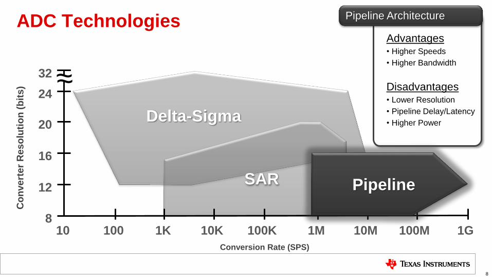
ADC Technologies
SAR
24
20
16
12
8
32
1K 100 10 10K 100K 1M 10M 100M 1G
Co
nve
rte
r R
es
olu
tio
n (
bit
s)
Conversion Rate (SPS)
Advantages • Higher Speeds
• Higher Bandwidth
Disadvantages • Lower Resolution
• Pipeline Delay/Latency
• Higher Power
Pipeline Architecture
Pipeline
Delta-Sigma
~ ~
8

SAR ADC takes “snapshots” Each conversion command captures the
signal level, at that point in time, onto the
sample/hold
ADC calculates an average The signal is sampled continuously
What is the ADC actually converting?
SAR vs. Delta-Sigma
SAR
9

• SAR conversions have Start Conversion Signal
• Delta-Sigma’s are always sampling/converting
SAR Converter
Start Conversion
Conversion Done
Delta-Sigma Converter
Input Sampling
Conversion Done
How does the ADC control happen?
SAR vs. Delta-Sigma
10

?
How Does a SAR ADC Work?
• Similar to a balance scale
½ ¼ 1
11

How Does a SAR ADC Work?
• Similar to a balance scale
½ ¼ 1
?
12
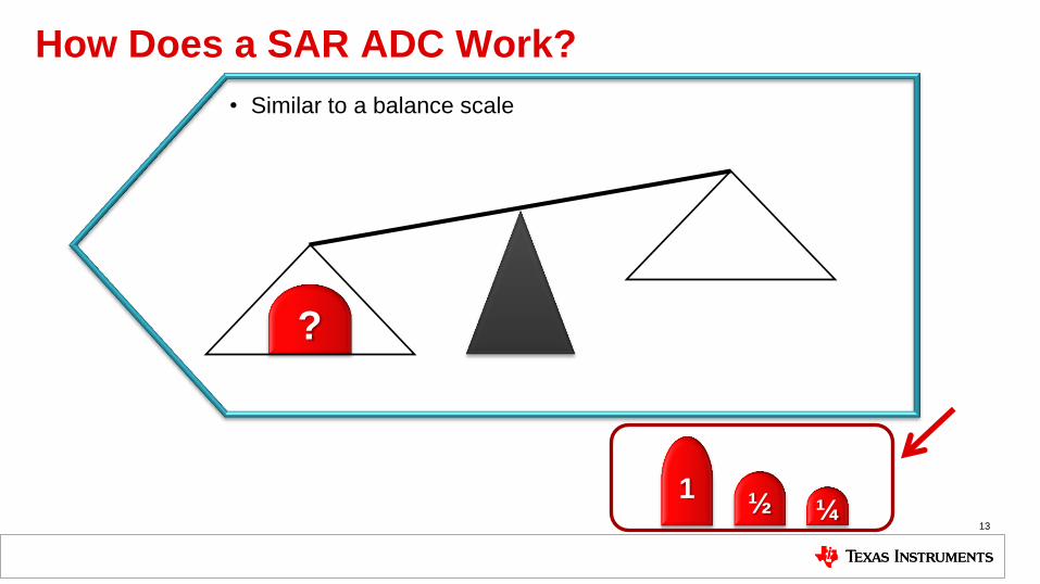
How Does a SAR ADC Work?
• Similar to a balance scale
½ ¼ 1
?
13

How Does a SAR ADC Work?
• Similar to a balance scale
½ ¼
? MSB
1
1
The MSB is determined first
14

How Does a SAR ADC Work?
• Similar to a balance scale
½
¼
?
MSB
1
1
The test is repeated for each
Binary weighted bit
Mid
0
15

How Does a SAR ADC Work?
• Similar to a balance scale
½
?
MSB
1
1
Mid
0
¼
LSB
1
The LSB is determined last
16

Typical Topology of a SAR ADC
17

SAR ADC Acquisition Phase
COMPARATOR
SAMPLE & HOLD
VIN DAC
C
S1
VIN
S2
N-bit Search
DAC
Data Register
SAR
18

SAR ADC Acquisition Phase
VSH0
VIN
tAQ Time
1/2 LSB
VCSH(t)
t0
COMPARATOR
SAMPLE & HOLD
VIN DAC
C
S1
VIN
S2
N-bit Search
DAC
Data Register
SAR
19

SAR ADC Acquisition Phase
)1()]([)()( 00
t
CSHINCSHCSH etVVtVtV
VSH0
VIN
tAQ Time
1/2 LSB
VCSH(t)
t0
SHS CR 1
COMPARATOR
SAMPLE & HOLD
VIN DAC
20

SAR ADC Conversion Phase
Analog
Input
VD
AC
FS
0
1/4FS
1/2FS
3/4FS
TEST
MSB
TEST
MSB -1
TEST
LSB
TEST
MSB -2
Bit = 1
Bit = 0
Bit = 1 Bit = 0
Digital Output Code = 10100
Time
Bit = 0
TEST
MSB -3
DAC Output 21

SAR ADCs
SAR ADC
22
• Very Popular Topology
• Attractive in “Point in Time” or Multiplexed Measurements
• Advantages
– “no latency”
• input is sampled once
• “balancing” done internally
– good tradeoff between speed, resolution and power
• Speed: DC to 5 MSPS
• Resolution: 8 to 20 bits
• TI Part Numbers: – ADC0x/1x – ADS7xxx – ADS8xxx – ADS9xxx

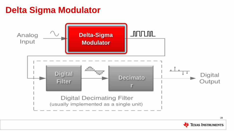
Delta-Sigma Topology
Delta-Sigma Modulator
Analog Input
Digital Filter
Decimator
Digital Output
Digital Decimating Filter
23
Delta-Sigma
Modulator
Digital
Filter Decimator
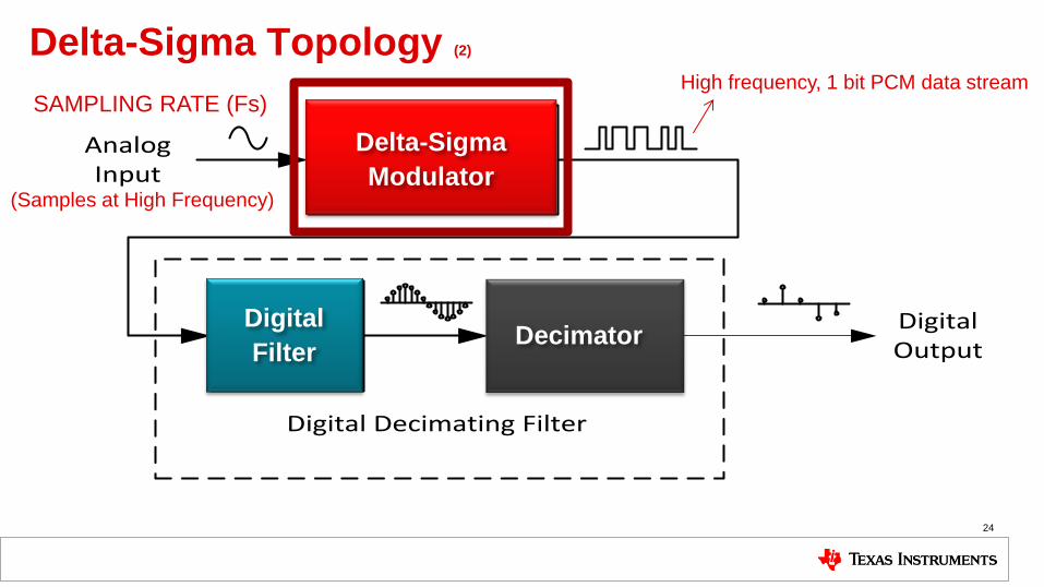
Delta-Sigma Topology (2)
Delta-Sigma Modulator
Analog Input
Digital Filter
Decimator
Digital Output
Digital Decimating Filter
SAMPLING RATE (Fs)
24
Delta-Sigma
Modulator
Digital
Filter Decimator
High frequency, 1 bit PCM data stream
(Samples at High Frequency)

Delta-Sigma Topology (3)
Delta-Sigma Modulator
Analog Input
Digital Filter
Decimator
Digital Output
Digital Decimating Filter
SAMPLING RATE (Fs)
DATA RATE (Fd)
25
Delta-Sigma
Modulator
High frequency, 1 bit PCM data stream
Lower data rate, very high
resolution digital output
Input Oversampling
Digital
Filter Decimator

26
Oversampling (1)
fs/2 fs
Power
Average Noise energy distributed from DC to
fs/2
Ideal N-Bit ADC SNR= 6.02 N + 1.76 dB
DC
Input Signal
Average Noise Floor

27
Oversampling (2)
– On a Delta-Sigma Converter, the analog input is sampled at a Frequency much higher than the Nyquist rate
fs/2 fs
Power
Average Noise energy distributed from DC to
fs/2
Ideal N-Bit ADC SNR= 6.02 N + 1.76 dB
DC
Input Signal
Average Noise Floor
Average Noise Floor
K fs/2 K fs
Power
Average Noise energy distributed over a wider range from DC to K fs/2
SNR= 6.02 N + 1.76 dB +10 log (OSR)
DC
Digital Low Pass filter
Oversampling
Delta Sigma Modulator
28
Delta-Sigma
Modulator
Digital
Filter Decimato
r

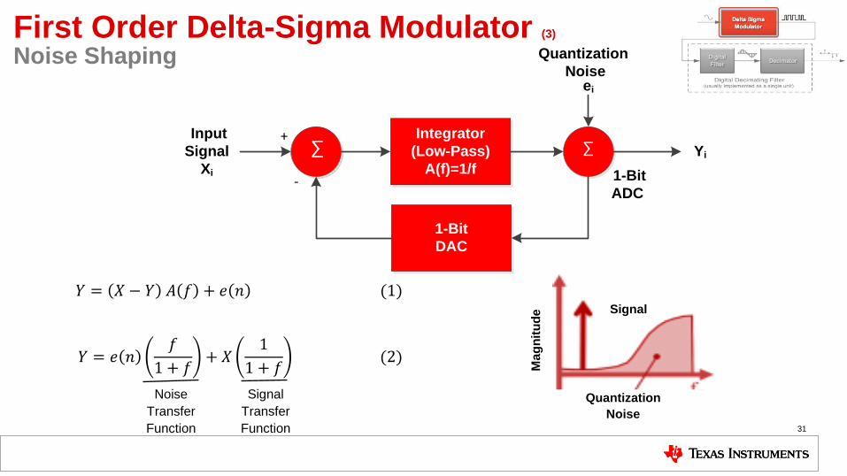
First Order Delta-Sigma Modulator (1)
Noise Shaping
Integrator
(Low-Pass)
A(f)=1/f
Input
Signal
Xi
∑ +
∑
-
ei
Quantization
Noise
1-Bit
ADC
1-Bit
DAC
Yi
29

First Order Delta-Sigma Modulator (2)
Noise Shaping
Noise
Transfer
Function
Signal
Transfer
Function
Integrator
(Low-Pass)
A(f)=1/f
Input
Signal
Xi
∑ +
∑
-
ei
Quantization
Noise
1-Bit
ADC
1-Bit
DAC
Yi
𝑌 = 𝑋 − 𝑌 𝐴 𝑓 + 𝑒 𝑛 (1)
𝑌 = 𝑒 𝑛𝑓
1 + 𝑓+ 𝑋
1
1 + 𝑓 (2)
30
First Order Delta-Sigma Modulator (3)
Noise Shaping
Signal
Ma
gn
itu
de
Quantization
Noise
Noise
Transfer
Function
Signal
Transfer
Function
Integrator
(Low-Pass)
A(f)=1/f
Input
Signal
Xi
∑ +
∑
-
ei
Quantization
Noise
1-Bit
ADC
1-Bit
DAC
Yi
𝑌 = 𝑋 − 𝑌 𝐴 𝑓 + 𝑒 𝑛 (1)
𝑌 = 𝑒 𝑛𝑓
1 + 𝑓+ 𝑋
1
1 + 𝑓 (2)
31

First Order Delta-Sigma Modulator (4)
Noise Shaping
Modulator Output: TIME DOMAIN
0
1
Believe it or not, the sine wave is in there!
(drawing is approximate)
Sig
nal
32

First Order Delta-Sigma Modulator (5)
Noise Shaping
Modulator Output: TIME DOMAIN
0
1
Believe it or not, the sine wave is in there!
(drawing is approximate)
Sig
nal
33
First Order Delta-Sigma Modulator (6)
Noise Shaping
Modulator Output: TIME DOMAIN
Modulator Output: FREQUENCY DOMAIN
0
1
Believe it or not, the sine wave is in there!
(drawing is approximate)
QUANTIZATION
NOISE
Fs
SIGNAL
Sig
nal
34

Frequency FS
Third Order
Modulator
Second Order
Modulator
First Order
Modulator
Higher Order Delta-Sigma Modulators
35

Delta-Sigma A/D Signal Path
36
Delta-Sigma
Modulator
Digital
Filter Decimator

Frequency FS
Modulator Noise Shaping and Digital Filter(1)
37
Modulator
Noise Shaping

Frequency FS
Modulator Noise Shaping and Digital Filter(2)
38
Modulator
Noise Shaping

Frequency FS
Modulator Noise Shaping and Digital Filter(3)
39
Filter set by
Oversampling
Ratio
Modulator
Noise Shaping
40
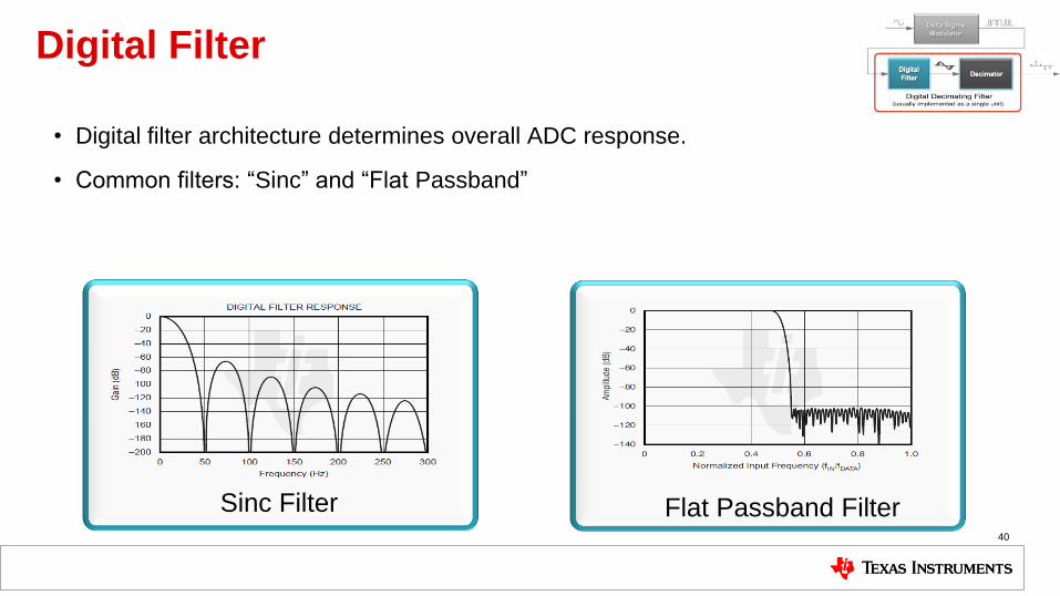
Digital Filter
• Digital filter architecture determines overall ADC response.
• Common filters: “Sinc” and “Flat Passband”
Sinc Filter Flat Passband Filter

41
Sinc Digital Filter
Sinc filter response
-100
-80
-60
-40
-20
0
0 1 2 3 4 5 6
Frequency (x Fdata)
Att
en
tua
tio
n, d
B
Sinc 1
Sinc 3
Sinc 5
• Typically used for DC measurements, or slow moving signals
Advantages
• Economical silicon area, easy to
implement
– Low cost
– Low power
• Low latency
• Filter notches can target specific
frequencies (ex. 50/60 Hz)
Disadvantages
• Pass band signal droop
• Weak Stop band attenuation for
low-order Sinc filters
Fdata

Sinc Digital Filter Settling
0 1 2 3 0 1 2 3
3 full cycles 3 full cycles
Valid data Valid data
Fdata periods
Analog Inputs
Settling time for an input step change, Sinc3 filter
Need n cycles to settle for a Sincn filter
4 cycles
Uncertainty of Analog Edge
4 Data Cycles
42

• Zero cycle Latency =
– Zero latency
– Single cycle conversion
– Single cycle settling
– No Latency
Analog IN
Data OUT
Single Cycle
Conversion
Data
Invalid
N+0 N+1 N+2 N+3 N-1
N+1 N+2
N+3 N+0
Delta-Sigma: Zero Cycle Latency (1)
43

• Zero cycle Latency =
– Zero cycle latency
– Single cycle conversion
– Single cycle settling
– No Latency
Analog IN
Data OUT
Single Cycle
Conversion
Data
Invalid
N+0 N+1 N+2 N+3 N-1
N+1 N+2
N+3 N+0
Delta-Sigma: Zero Cycle Latency (2)
“Hidden Conversions”
44

45
Flat Pass Band Filter
Advantages
• Frequency Response
• Very low ripple pass band
• Sharp Nyquist transition band
• Large stopband attenuation: lower than
-100dB (simplify aliasing requirement)
• Frequency response scalable with master
clock
Disadvantages
• Large area – Costly
• Higher-order / high-tap filter – large latency
100dB stop band
Low Ripple Passband

46
Delta-Sigma: Flat Passband Digital Filter Settling
• The latency of the filter depends on the number of delay blocks used
• Flat Passband filters require a lot delay blocks to maintain desired AC response
• Many Delta-Sigma Converters incorporate filters with programmable settings: – Optimize for lower latency, power consumption or for AC performance/higher resolution
delay delay delay delay delay
Σ
Modulator Data Input
Digital Filter
Output
FIR filter block
topology
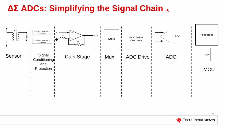
ΔΣ ADCs: Simplifying the Signal Chain (1)
CT
Passive Network + Protection
Passive Network + Protection +
R1
R2
In
OutADC Drive Circuitry
Iso
ADCProcessor
MUX
Sensor Signal
Conditioning
and
Protection
Gain Stage Mux ADC Drive ADC
MCU
47

ΔΣ ADCs: Simplifying the Signal Chain (2)
CT
Passive Network + Protection
Passive Network + Protection +
R1
R2
In
OutADC Drive Circuitry
Iso
ADCProcessor
MUX
Sensor Signal
Conditioning
and
Protection
Gain Stage Mux ADC Drive ADC
MCU
Delta-Sigma ADCs integrate many signal chain elements into one device 48
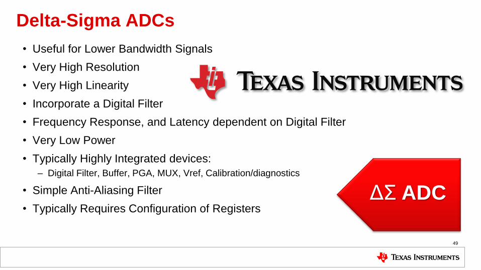
Delta-Sigma ADCs
• Useful for Lower Bandwidth Signals
• Very High Resolution
• Very High Linearity
• Incorporate a Digital Filter
• Frequency Response, and Latency dependent on Digital Filter
• Very Low Power
• Typically Highly Integrated devices:
– Digital Filter, Buffer, PGA, MUX, Vref, Calibration/diagnostics
• Simple Anti-Aliasing Filter
• Typically Requires Configuration of Registers
49
ΔΣ ADC
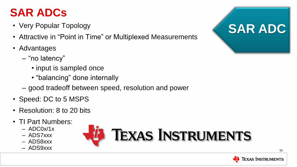
SAR ADCs • Very Popular Topology
• Attractive in “Point in Time” or Multiplexed Measurements
• Advantages
– “no latency”
• input is sampled once
• “balancing” done internally
– good tradeoff between speed, resolution and power
• Speed: DC to 5 MSPS
• Resolution: 8 to 20 bits
• TI Part Numbers: – ADC0x/1x – ADS7xxx – ADS8xxx – ADS9xxx
SAR ADC
50

Input Driver Circuit for SAR ADC
51
CF is an ideal source to
high frequency transients
HIGH GBW Faster load transient response
+
-
C
S1 S2
N-bit Search
DAC
Data Register
SAR
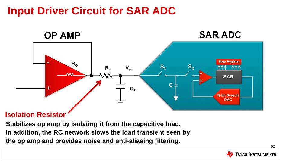
Input Driver Circuit for SAR ADC
52
+
-
C
S1 S2
N-bit Search
DAC
Data Register
SAR
Isolation Resistor
Stabilizes op amp by isolating it from the capacitive load.
In addition, the RC network slows the load transient seen by
the op amp and provides noise and anti-aliasing filtering.

Fully Differential ADC Inputs
ΔΣ ADC
Core
24-bit
512 kSPS
Passband: 230 kHz
115.5 dB SNR
-129 dB THD
On Chip
Decimation
Filter
Input Range
Differential Input
Vin: ±VREF
ADS127L01
SPI & Frame-
Sync Digital
Interface
5-pin SPI
Daisy Chain
Capable
AINN
AINP
+
-
- +
THS4551
THS4551 Based Single-Ended Input to Differential Output with
Multiple Feedback Filter Interface to the 24-bit, 512 kSPS ADS127L01 Delta-Sigma ADC
53
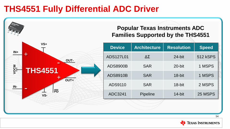
THS4551 Fully Differential ADC Driver
Popular Texas Instruments ADC
Families Supported by the THS4551
VO
CM
VS+
VS-
OUT+
OUT-
IN+
IN-
+
-
-
+ THS4551
PD
Device Architecture Resolution Speed
ADS127L01 ΔΣ 24-bit 512 kSPS
ADS8900B SAR 20-bit 1 MSPS
ADS8910B SAR 18-bit 1 MSPS
ADS9110 SAR 18-bit 2 MSPS
ADC3241 Pipeline 14-bit 25 MSPS
54

More Analog Signal Chain Information Precision ADC Web Page: www.ti.com/precisionadc
Fully Differential Amplifier Web Page: www.ti.com/fda
• Data Sheets & Technical Reference Manuals
• Application Notes
• Software, Tools & SPICE Model Downloads
• Order Evaluation & Performance Demonstration Kits
Precision ADC E2E™ Support Forum:
www.ti.com/precisionadcsupport
• Ask Technical Questions
• Search for Technical Content
Precision HUB Blog Series:
e2e.ti.com/blogs_/b/precisionhub
Tips, tricks and techniques
from TI precision analog experts
TI Designs - Precision:
www.ti.com/precisiondesigns
• Reference Designs
• Board Schematics & Verification Results
55

56
Special Thanks
Special thanks to the following people for contributing to this presentation:
• Ryan Callaway – Delta-Sigma ADC
• Tony Calabria – Delta-Sigma ADC
• Anthony Vaughan – High Speed Amplifiers
• Michael Steffes – High Speed Amplifiers
• Luis Choye – SAR ADC
• Vinay Agarwal – SAR ADC
11001101011010
10101010101010
10101010111010
01010011101101
010101