Sanghoon Shin and Sridhar Kanamalurutech.mweda.com/download/hwrf/hfss/EM.pdf · Filter T-Junction...
8
April 2007 77 1527-3342/07/$25.00©2007 IEEE Sanghoon Shin is with R.S. Microwave Inc., Butler, NJ, USA. Sridhar Kanamaluru ([email protected]) is with Herley Industries, Inc., Lancaster, PA, USA. T hree-dimensional (3-D) electromagnetic (EM) simulators provide simulation results that are close to measurements when used in the design of passive components such as RF filters, multiplexers, couplers, and anten- nas. However, when the analyzed structure is complex and/or when tuning and optimization are involved, EM simulators require more computation time than circuit- based simulators. This article investigates a technique utilizing the strengths of both EM- and circuit-based simulators (i.e., EM circuit cosimulation) to provide accurate results with reduced computation times. EM Circuit Cosimulation Technique Figure 1 shows the basic concept of the EM circuit cosimulation technique. Rather than analyzing the entire physical structure using an EM simulator, the structure is first separated into discrete components and EM analysis is performed individually. Each component’s EM analysis is carried out for a range of design variables (e.g., length, width, height, corner radius, and frequency) with fixed intervals (i.e., step size). The results are saved as a numerical EM model, and could be a parameterized scattering matrix [neutral model format (NMF)] [1] or a link available on call to a circuit simulator. Interpolation of the EM results is carried out for specific values of the vari- ables that have not been previously simulated. Ideally, most structures could be separated into a standard set of components (e.g., T-junction, bend, and step discontinuity), and the EM models are avail- able a priori. Sanghoon Shin and Sridhar Kanamaluru © IMAGESTATE
Transcript of Sanghoon Shin and Sridhar Kanamalurutech.mweda.com/download/hwrf/hfss/EM.pdf · Filter T-Junction...
April 2007 771527-3342/07/$25.00©2007 IEEE
Sanghoon Shin is with R.S. Microwave Inc., Butler, NJ, USA. Sridhar Kanamaluru ([email protected])
is with Herley Industries, Inc., Lancaster, PA, USA.
Three-dimensional (3-D) electromagnetic(EM) simulators provide simulation resultsthat are close to measurements when usedin the design of passive components such asRF filters, multiplexers, couplers, and anten-
nas. However, when the analyzed structure is complexand/or when tuning and optimization are involved, EMsimulators require more computation time than circuit-based simulators. This article investigates a techniqueutilizing the strengths of both EM- and circuit-basedsimulators (i.e., EM circuit cosimulation) to provideaccurate results with reduced computation times.
EM Circuit Cosimulation TechniqueFigure 1 shows the basic concept of the EM circuitcosimulation technique. Rather than analyzing the
entire physical structure using an EM simulator, thestructure is first separated into discrete componentsand EM analysis is performed individually. Eachcomponent’s EM analysis is carried out for a range ofdesign variables (e.g., length, width, height, cornerradius, and frequency) with fixed intervals (i.e., stepsize). The results are saved as a numerical EM model,and could be a parameterized scattering matrix[neutral model format (NMF)] [1] or a link availableon call to a circuit simulator. Interpolation of the EMresults is carried out for specific values of the vari-ables that have not been previously simulated.Ideally, most structures could be separated into astandard set of components (e.g., T-junction, bend,and step discontinuity), and the EM models are avail-able a priori.
Sanghoon Shin and Sridhar Kanamaluru
©IM
AG
ES
TAT
E

78 April 2007
To analyze the entire structure, a circuit-based simu-lator is used. This simulator uses a combination of EM-and circuit-based models, and the optimization is car-ried out using the circuit simulator. Thus, EM analysis
for every combination of dimensions can be avoidedduring optimization, and faster simulation speed isachieved. Also, circuit-simulator-based tuning is madeavailable, and the results can be viewed in real time.
At the final design stage, the cosimulated result isvalidated with a full EM simulation of the entire struc-ture using the optimized values to confirm the cosimu-lated result. Thus, full EM simulation of the entire struc-ture is performed just for analysis and not for optimiza-tion or tuning. Using this cosimulation technique, EMsimulation type accuracy can be obtained with a circuitsimulation speed.
Various 3-D EM field solvers [finite element method(FEM), finite differencemethod (FDM), finite differ-ence time domain (FDTD),mode-matching] are com-mercially available, and eachsolver is particularly applica-ble for specific structures andapplications. Therefore, inpractice, no commercial 3-DEM simulator covers allapplications, and it is cost-prohibitive to use all EMsolvers. In this article, we usea general FEM 3-D EM solverand circuit simulator todesign a diplexer and intro-duce the EM circuit cosimula-tion approach.
Diplexer DesignTo demonstrate the EM circuit cosimulation method,H-plane waveguide diplexers, shown in Figure 2, arepresented as design examples. The design require-ments are as follows:
Center frequency: 7.5 GHz for Channel 18.15 GHz for Channel 2
Bandwidth: 500 MHz eachWaveguide: WR112
1.112 in (w) × 0.497 in (h)Passband return loss: 18 dB min
Two different diplexer configura-tions are designed: the L-shape diplexer[Figure 2(a)] and the T-shape diplexer[Figure 2(b)]. In each diplexer, twochannel filters are combined with theinput common port through a T-junc-tion. Thus, the diplexer can be dividedinto two major sections: the waveguidechannel filters and the T-junction. EachT-junction and waveguide channel fil-ter will be designed separately andcombined for circuit-simulator-based
Figure 1. EM circuit cosimulation.
Specifications
• Frequency
• Insertion Loss
• Return Loss
• Isolation
• Power Handling
• Use Circuit Models
• Call/Retrieve EM-Models
• Physical Dimension Optimization to Meet Specifications
Structure Defn.• Define Structure
• Identify Discrete Components
• Define Design Variables and Ranges
Circuit Simulator
SimilarResults
EM Simulator• Full-Wave Analysis
• Parametric Analysis
• Field Plots
• Parameterized S-Matrix or
• EM Geometry
• Physics Effects (e.g., Thermal Analysis)
EM-Based Models
Figure 3. Decomposed elements of diplexers.
1
32 Ch.1Filter
T-Junction Ch.2Filter
(a)
1 3
2
Ch.1Filter
Ch.2Filter
T-Junction
(b)
At the final design stage, the cosimulated result is validatedwith a full EM simulation of the entirestructure using the optimized valuesto confirm the cosimulated result.
Figure 2. H-plane waveguide diplexers.
Ch.2
Input
Ch.1
(a)
Ch.2
Input
Ch.1(b)

April 2007 79
optimization. Figure 3 shows each component requiredfor cosimulation [2]. In [2] and [3], thediplexer structure is analyzed using amode-matching method with a generalizedscattering matrix. A similar approach isapplied here.
T-Junction DesignThe first step in the EM circuit cosimula-tion method is the T-junction design.Figure 4 shows an H-plane T-junction witha symmetric septum. The T-junction is athree-port device, which connects the twoTE01 dominant mode waveguide channelfilters to the common input port. In thiscase, the design parameter is the length ofthe septum. By changing the length of theseptum (L) and the connecting waveguidearm length, maximum power will betransmitted to each channel filter.
To standardize the EM results for vari-ous combinations of dimensions duringlater use in the circuit simulator, the EMresults are de-embedded up to thereference planes shown in Figure 4. Thisport de-embedding also elim-inates possible higher-ordermode reflection near thejunction into the wave ports.For later circuit-simulator-based optimization, a para-metric sweep simulation isperformed by changing theseptum length from 0.15 to0.55 in using 0.1-in intervals(five steps). Then, this precal-culated parametric EMmodel is inserted into the cir-cuit schematic and optimizedto define a septum lengththat provides maximumtransmission at each chan-
nel’s frequencies into the appropriate port. The entireT-junction response is validated with the 3-D EM solverusing the calculated septum length from the circuitdomain optimizer. Figure 5 is a full wave analyzedresult using the optimized septum length from the cir-cuit simulator.
Figure 4. H-plane T-junction and waveport de-embedding:(a) 3-D view and (b) top view for T-connection.
(a)
Input(Port 1)
Ch.1(Port 2)
Ch.2(Port 3)L
Port De-embeddingReference Planes
(b)
When the analyzed structure iscomplex and/or when tuning and
optimization is involved, EMsimulators require more computation
time than circuit-based simulators.
Figure 6. Cosimulation schematic for decomposed seventh-order Chebyshev waveguidechannel filter.
1) Half Wavelength Waveguide Section from Circuit Model
2) Parameterized Full Wave EM Model for Inductive Window Coupling Generated by EM Solver
Figure 5. H-plane T junction model response of EM simulator using theoptimized septum length (L) on the circuit domain.
X1 = 7.50 GHzY1 = −3.08
X2 = 7.50 GHzY2 = −3.08
X3 = 7.50 GHzY3 = −17.99
Y1dB(S(p1,p1)) [dB]Setup1: Sweep1
Y1dB(S(p2,p1)) [dB]Setup1: Sweep1
Y1dB(S(p3,p1)) [dB]Setup1: Sweep1
TeeModel_wr112_opt0.00
−5.00
−10.00
−15.00
−20.006.50 7.00 7.50 8.00 8.50 9.00
s11,
s21
, s31
, (dB
)
Freq [GHz]
3
2
Waveguide Filter DesignThe second step in the cosimulation technique is thedesign of waveguide channel filters. A seven-section0.01-dB ripple doubly terminated Chebyshev wave-guide filter is used for demonstration. To design thewaveguide channel filter, the entire filter structurecan be decomposed into the half-wavelength res-onator section and inductive iris window couplingsection, as shown in Figure 6 [3]. For resonator sec-tions, the TE01 dominant mode rectangular wave-guide model in the circuit simulator library is used.For the inductive window coupling, a parameterizedEM model will be generated with the EM solver. Byvarying the window width from 0.15 in to 0.9 in using
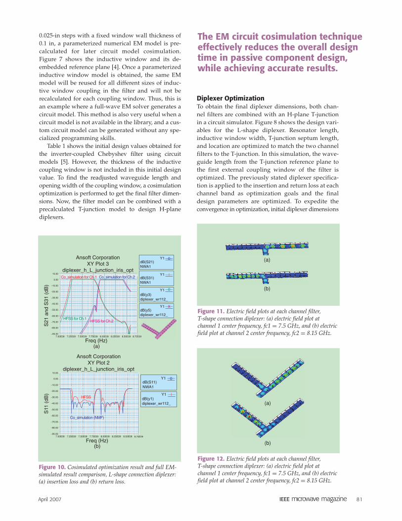
TABLE 1. Initial filter design.(a) Ch1.Filter, fc1 = 7,500 MHz, BW = 500 MHz.
Resonator Cavity Inductive No. Length (in) Window (in)
1 0.8703 0.63 Ext. coupling
2 0.9895 0.3894 Int. coupling
3 1.015 0.3288 Int. coupling
4 1.018 0.3175 Int. coupling
5 1.015 0.3175 Int. coupling
6 0.9895 0.3288 Int. coupling
7 0.8703 0.3894 Int. coupling
0.63 Ext. coupling
Figure 9. Cosimulated optimization result and full EMsimulated result comparison, T-shape connection diplexer:(a) insertion loss and (b) return loss.
dB(y1)HFSS_diplexer_y
lY1
Y1 0
Ansoft CorporationXY Plot 2
diplexer_T_T_iris1_h_opti1_silver
7.00E09 7.25E09 7.50E09 7.75E09 8.00E09
Freq (Hz)8.25E09 8.50E09 8.75E09
0.00
−10.00
−20.00
Co_simulation(NMF)HFSS
−30.00S11
(dB
)
−40.00
−50.00
10.00
Ansoft CorporationXY Plot 1
diplexer_T_T_iris1_h_opti1_silver
HFSS for Ch.1
7.00E09 7.25E09 7.50E09 7.75E09 8.00E09
Freq (Hz)8.25E09 8.50E09 8.75E09
S21
and
S31
(dB
)
HFSS for Ch.2
0.00
−10.00
−20.00
−30.00
−40.00
−50.00
−60.00
−70.00
−80.00
−90.00
ldB(S31)Designer
Y1
dB(y3)HFSS_diplexer_y
Y1 0
dB(y5)HFSS_diplexer_y
Y1 X
dB(S21)Designer
Co-simulation for Ch.1 Co-simulation for Ch.2
(a)
(b)
dB(S11)NMA1
Y1 0
The circuit-based simulator uses acombination of EM- and circuit-basedmodels, and the optimization iscarried out using the circuit simulator.
(b) ch2. Filter, fc1 = 8150 MHz, BW = 500 MHz
Resonator Cavity Inductive No. Length (in) Window width (in)
1 0.772 0.55 Ext. coupling
2 0.8691 0.3258 Int. coupling
3 0.8866 0.2763 Int. coupling
4 0.8891 0.2671 Int. coupling
5 0.8866 0.2671 Int. coupling
6 0.8691 0.2763 Int. coupling
7 0.772 0.3258 Int. coupling
0.55 Ext. coupling
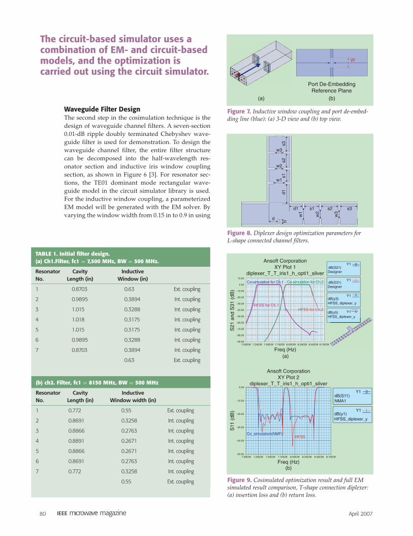
Figure 8. Diplexer design optimization parameters for L-shape connected channel filters.
w3
w2
w1
d1s1
s2s3
d
d1 s1 s2 s3
w1
w2
w3
h
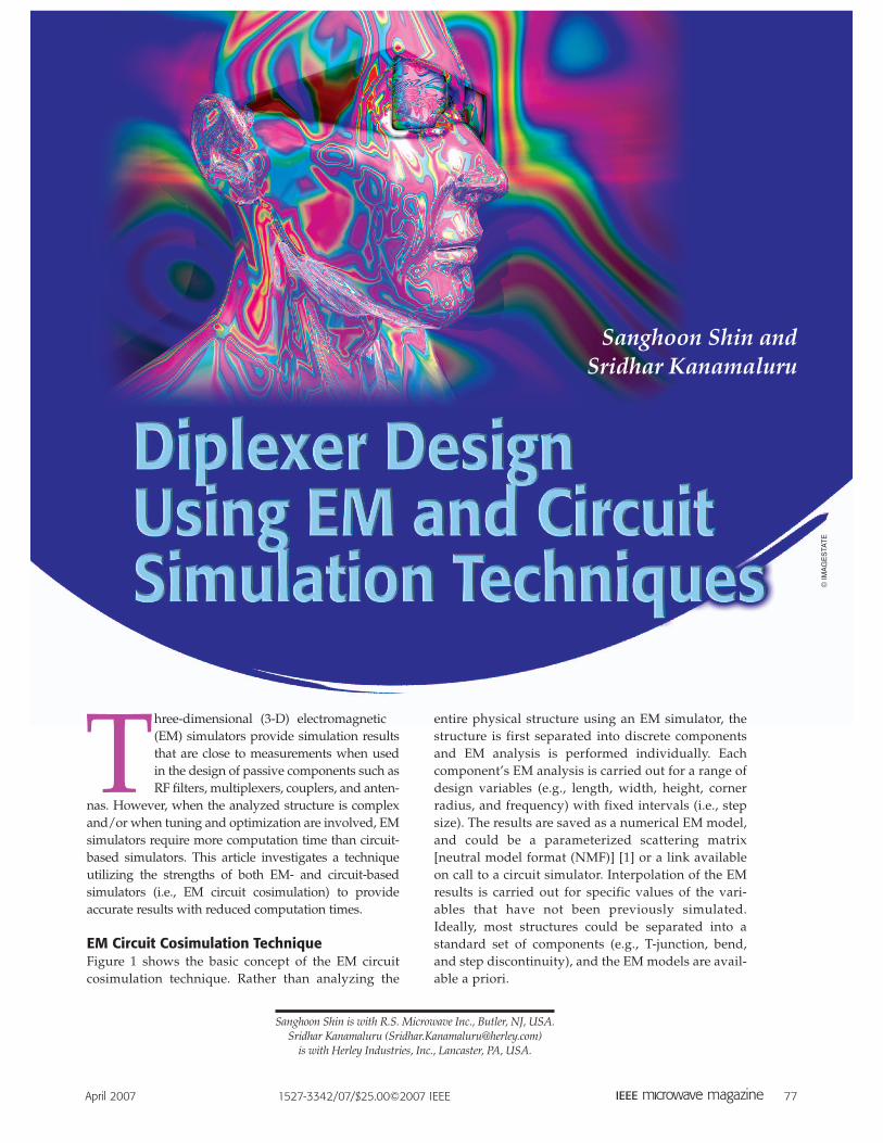
Figure 7. Inductive window coupling and port de-embed-ding line (blue): (a) 3-D view and (b) top view.
p11
(a)
Port De-EmbeddingReference Plane
W
(b)
80 April 2007
April 2007 81
0.025-in steps with a fixed window wall thickness of0.1 in, a parameterized numerical EM model is pre-calculated for later circuit model cosimulation.Figure 7 shows the inductive window and its de-embedded reference plane [4]. Once a parameterizedinductive window model is obtained, the same EMmodel will be reused for all different sizes of induc-tive window coupling in the filter and will not berecalculated for each coupling window. Thus, this isan example where a full-wave EM solver generates acircuit model. This method is also very useful when acircuit model is not available in the library, and a cus-tom circuit model can be generated without any spe-cialized programming skills.
Table 1 shows the initial design values obtained forthe inverter-coupled Chebyshev filter using circuitmodels [5]. However, the thickness of the inductivecoupling window is not included in this initial designvalue. To find the readjusted waveguide length andopening width of the coupling window, a cosimulationoptimization is performed to get the final filter dimen-sions. Now, the filter model can be combined with aprecalculated T-junction model to design H-planediplexers.
Diplexer OptimizationTo obtain the final diplexer dimensions, both chan-nel filters are combined with an H-plane T-junctionin a circuit simulator. Figure 8 shows the design vari-ables for the L-shape diplexer. Resonator length,inductive window width, T-junction septum length,and location are optimized to match the two channelfilters to the T-junction. In this simulation, the wave-guide length from the T-junction reference plane tothe first external coupling window of the filter isoptimized. The previously stated diplexer specifica-tion is applied to the insertion and return loss at eachchannel band as optimization goals and the finaldesign parameters are optimized. To expedite theconvergence in optimization, initial diplexer dimensions
Figure 10. Cosimulated optimization result and full EM-simulated result comparison, L-shape connection diplexer:(a) insertion loss and (b) return loss.
Y1 0dB(S21)NWA1
ldB(S31)NWA1
Y1
dB(y3)diplexer_wr112_
Y1 0
dB(y5)diplexer_wr112_
Y1 X
dB(S11)NWA1
Y1 0
lY1dB(y1)diplexer_wr112_
10.00
Ansoft CorporationXY Plot 2
diplexer_h_L_junction_iris_opt
7.00E09 7.25E09 7.50E09 7.75E09 8.00E09
Freq (Hz)8.25E09 8.50E09 8.75E09
S11
(dB
)
HFSS
0.00
−10.00
−20.00
−30.00
−40.00
−50.00
−60.00
−70.00
−80.00
−90.00
(b)
Co_simulation (NMF)
10.00
Ansoft CorporationXY Plot 3
diplexer_h_L_junction_iris_opt
HFSS for Ch.1
7.00E09 7.25E09 7.50E09 7.75E09 8.00E09
Freq (Hz)8.25E09 8.50E09 8.75E09
S21
and
S31
(dB
)
HFSS for Ch.2
0.00
−10.00
−20.00
−30.00
−40.00
−50.00
−60.00
−70.00
−80.00
−90.00
Co_simulation for Ch.1 Co_simulation for Ch.2
(a)
The EM circuit cosimulation techniqueeffectively reduces the overall designtime in passive component design,while achieving accurate results.
Figure 12. Electric field plots at each channel filter, T-shape connection diplexer: (a) electric field plot at channel 1 center frequency, fc1 = 7.5 GHz, and (b) electricfield plot at channel 2 center frequency, fc2 = 8.15 GHz.
(b)
(a)
Figure 11. Electric field plots at each channel filter, T-shape connection diplexer: (a) electric field plot at channel 1 center frequency, fc1 = 7.5 GHz, and (b) electricfield plot at channel 2 center frequency, fc2 = 8.15 GHz.
(a)
(b)

82 April 2007
must be close to the final values. Otherwise, the opti-mization result will take a long time to converge or itmay not converge.
Figures 9 and 10 show final optimized cosimulationresults. A final EM simulation of the entire physicalstructure is carried out to compare and validate the cir-cuit-based results with the EM-based results.
PostprocessingAn advantage of 3-D EM simulators is the availabili-ty of field plots for the volume inside the filter struc-ture. Figures 11 and 12 show the electric field plots ateach filter’s center frequency. From the field distribu-tion, the peak electric field area inside the diplexercan be displayed, which in turn relates to the maxi-mum peak power inside the filter structure [6]. Amagnetic (H)-field plot provides the high currentareas that relate to the average power handlingcapacity.
Thermal AnalysisThe temperature of the filter plays an importantrole in its performance. The temperature of the filteris related to the ambient temperature and the tem-perature rise due to excessive power. When exces-sively high power levels are applied to the filter, orwhen the unit is exposed to high ambient tempera-tures, the filter structure is faced with structuraldeformations. As a result, the filter response isdetuned from the nominal response. Typically, thefrequency drift range is confirmed by measuringthe filter response. Temperature-compensatingmaterials or structures could be used at this stage, ifwarranted. If software that can accurately predictthe environmental effects is available, the iterative
design cycles between manufacturing and measure-ment can be reduced.
Figure 13 shows the inside temperature data atsteady state when 1 kW average power is applied tothe common input port of the diplexer at a channel 1passband edge frequency (7.72 GHz). Hot and coolspots inside the diplexer are displayed using AnsoftePhysics thermal analysis software. Due to the powerdissipation on the inside conductor surface of thewaveguide, surface temperature rises up to about 90 ◦C.Figure 14 shows the time it takes for the filter to reachthe highest temperature from 0 ◦C using transient ther-mal analysis. However, the temperature drift responseof the diplexer from the structural deformation by heatis not yet available; this function is currently underdevelopment.
ConclusionThe EM circuit cosimulation technique effectivelyreduces the overall design time in passive componentdesign, while achieving accurate results. This methodcan be extended to other passive component designs,such as comb-line filter and dielectric resonator filter,with a higher-order mode waveport calculation.
References[1] D. Crawford, “Designing high performance cavity filters,” Ansoft
2003/Global Seminars [Online]. Available: www.ansoft.com[2] Y. Rong, H.-W. Yao, K.A. Zaki, and T.G. Dolan, “Millimeter-wave
Ka-band H-plane diplexers and multiplexers,” IEEE Trans.Microwave Theory Tech., vol. 47, no. 12, pp. 2,325–2,330, Dec. 1999.
[3] H.-W. Yao, A.E. Abdelmonem, J.-F. Liang, X.-P. Liang, K.A. Zaki,and A. Martin, “Wide-band waveguide and ridge waveguide T-junctions for diplexer applications,” IEEE Trans. Microwave TheoryTech., vol. 41, no. 12, pp. 2,166–2,173, Dec. 1993.
[4] F.M. Vanin, D. Schmitt, and R. Levy, “Dimensional synthesis forwide-band waveguide filters and diplexers,” IEEE Trans.Microwave Theory Tech., vol. 52, no. 11, pp. 2,488–2,495, Nov. 2004.
[5] Ansoft Designer [Online]. Available: www.ansoft.com[6] C. Wang and K.A. Zaki, “Analysis of power handling capacity of
band pass filters,” in 2001 IEEE MTT-S Int. Microwave Symp. Dig.,May 2001, vol. 3, pp. 1,611–1,614.
An advantage of 3-D EM simulators is the availability of field plots for thevolume inside the filter structure.
Figure 13. Temperature data inside the diplexer.
Temperature [°C]
9. 5190e+0019. 3165e+0019. 1140e+0018. 9115e+0018. 7090e+0018. 5064e+0018. 3039e+0018. 1014e+0017. 8989e+0017. 6964e+0017. 4939e+0017. 2914e+0017. 0889e+0016. 8864e+0016. 6838e+0016. 4813e+0016. 2788e+001
Figure 14. Transient thermal analysis of the temperatureof the diplexer.
diplexer_wr112_full_size1
Avg
Val
(WG
) [°
C]
80.00
60.00
40.00
20.00
0.000.00 2,000.00 4,000.00 6,000.00 8,000.00
Time [s]

专注于微波、射频、天线设计人才的培养 易迪拓培训 网址:http://www.edatop.com
射 频 和 天 线 设 计 培 训 课 程 推 荐
易迪拓培训(www.edatop.com)由数名来自于研发第一线的资深工程师发起成立,致力并专注于微
波、射频、天线设计研发人才的培养;我们于 2006 年整合合并微波 EDA 网(www.mweda.com),现
已发展成为国内最大的微波射频和天线设计人才培养基地,成功推出多套微波射频以及天线设计经典
培训课程和 ADS、HFSS 等专业软件使用培训课程,广受客户好评;并先后与人民邮电出版社、电子
工业出版社合作出版了多本专业图书,帮助数万名工程师提升了专业技术能力。客户遍布中兴通讯、
研通高频、埃威航电、国人通信等多家国内知名公司,以及台湾工业技术研究院、永业科技、全一电
子等多家台湾地区企业。
易迪拓培训课程列表:http://www.edatop.com/peixun/rfe/129.html
射频工程师养成培训课程套装
该套装精选了射频专业基础培训课程、射频仿真设计培训课程和射频电
路测量培训课程三个类别共 30 门视频培训课程和 3 本图书教材;旨在
引领学员全面学习一个射频工程师需要熟悉、理解和掌握的专业知识和
研发设计能力。通过套装的学习,能够让学员完全达到和胜任一个合格
的射频工程师的要求…
课程网址:http://www.edatop.com/peixun/rfe/110.html
ADS 学习培训课程套装
该套装是迄今国内最全面、最权威的 ADS 培训教程,共包含 10 门 ADS
学习培训课程。课程是由具有多年 ADS 使用经验的微波射频与通信系
统设计领域资深专家讲解,并多结合设计实例,由浅入深、详细而又
全面地讲解了 ADS 在微波射频电路设计、通信系统设计和电磁仿真设
计方面的内容。能让您在最短的时间内学会使用 ADS,迅速提升个人技
术能力,把 ADS 真正应用到实际研发工作中去,成为 ADS 设计专家...
课程网址: http://www.edatop.com/peixun/ads/13.html
HFSS 学习培训课程套装
该套课程套装包含了本站全部 HFSS 培训课程,是迄今国内最全面、最
专业的HFSS培训教程套装,可以帮助您从零开始,全面深入学习HFSS
的各项功能和在多个方面的工程应用。购买套装,更可超值赠送 3 个月
免费学习答疑,随时解答您学习过程中遇到的棘手问题,让您的 HFSS
学习更加轻松顺畅…
课程网址:http://www.edatop.com/peixun/hfss/11.html
`

专注于微波、射频、天线设计人才的培养 易迪拓培训 网址:http://www.edatop.com
CST 学习培训课程套装
该培训套装由易迪拓培训联合微波 EDA 网共同推出,是最全面、系统、
专业的 CST 微波工作室培训课程套装,所有课程都由经验丰富的专家授
课,视频教学,可以帮助您从零开始,全面系统地学习 CST 微波工作的
各项功能及其在微波射频、天线设计等领域的设计应用。且购买该套装,
还可超值赠送 3 个月免费学习答疑…
课程网址:http://www.edatop.com/peixun/cst/24.html
HFSS 天线设计培训课程套装
套装包含 6 门视频课程和 1 本图书,课程从基础讲起,内容由浅入深,
理论介绍和实际操作讲解相结合,全面系统的讲解了 HFSS 天线设计的
全过程。是国内最全面、最专业的 HFSS 天线设计课程,可以帮助您快
速学习掌握如何使用 HFSS 设计天线,让天线设计不再难…
课程网址:http://www.edatop.com/peixun/hfss/122.html
13.56MHz NFC/RFID 线圈天线设计培训课程套装
套装包含 4 门视频培训课程,培训将 13.56MHz 线圈天线设计原理和仿
真设计实践相结合,全面系统地讲解了 13.56MHz线圈天线的工作原理、
设计方法、设计考量以及使用 HFSS 和 CST 仿真分析线圈天线的具体
操作,同时还介绍了 13.56MHz 线圈天线匹配电路的设计和调试。通过
该套课程的学习,可以帮助您快速学习掌握 13.56MHz 线圈天线及其匹
配电路的原理、设计和调试…
详情浏览:http://www.edatop.com/peixun/antenna/116.html
我们的课程优势:
※ 成立于 2004 年,10 多年丰富的行业经验,
※ 一直致力并专注于微波射频和天线设计工程师的培养,更了解该行业对人才的要求
※ 经验丰富的一线资深工程师讲授,结合实际工程案例,直观、实用、易学
联系我们:
※ 易迪拓培训官网:http://www.edatop.com
※ 微波 EDA 网:http://www.mweda.com
※ 官方淘宝店:http://shop36920890.taobao.com
专注于微波、射频、天线设计人才的培养
官方网址:http://www.edatop.com 易迪拓培训 淘宝网店:http://shop36920890.taobao.com