
Samsung Exynos 5250 User Manual Public
881
Exynos 5250 RISC Microprocessor Revision 1.00 October 2012 U U s s e e ' ' r r M M a a n n u u a a l l 2012 Samsung Electronics Co., Ltd. All rights reserved.
-
Upload
agu-agumonkey -
Category
Documents
-
view
157 -
download
6
Transcript of Samsung Exynos 5250 User Manual Public

Exynos 5250
RISC Microprocessor
Revision 1.00
October 2012
UUssee''rr MMaannuuaall
2012 Samsung Electronics Co., Ltd. All rights reserved.
Important Notice
Samsung Electronics Co. Ltd. (“Samsung”) reserves the
right to make changes to the information in this publication
at any time without prior notice. All information provided is
for reference purpose only. Samsung assumes no
responsibility for possible errors or omissions, or for any
consequences resulting from the use of the information
contained herein.
This publication on its own does not convey any license,
either express or implied, relating to any Samsung and/or
third-party products, under the intellectual property rights of
Samsung and/or any third parties.
Samsung makes no warranty, representation, or guarantee
regarding the suitability of its products for any particular
purpose, nor does Samsung assume any liability arising out
of the application or use of any product or circuit and
specifically disclaims any and all liability, including without
limitation any consequential or incidental damages.
Customers are responsible for their own products and
applications. "Typical" parameters can and do vary in
different applications. All operating parameters, including
"Typicals" must be validated for each customer application
by the customer's technical experts.
Samsung products are not designed, intended, or authorized
for use in applications intended to support or sustain life, or
for any other application in which the failure of the Samsung
product could reasonably be expected to create a situation
where personal injury or death may occur. Customers
acknowledge and agree that they are solely responsible to
meet all other legal and regulatory requirements regarding
their applications using Samsung products notwithstanding
any information provided in this publication. Customer shall
indemnify and hold Samsung and its officers, employees,
subsidiaries, affiliates, and distributors harmless against all
claims, costs, damages, expenses, and reasonable attorney
fees arising out of, either directly or indirectly, any claim
(including but not limited to personal injury or death) that
may be associated with such unintended, unauthorized
and/or illegal use.
WARNING No part of this publication may be reproduced,
stored in a retrieval system, or transmitted in any form or by
any means, electric or mechanical, by photocopying,
recording, or otherwise, without the prior written consent of
Samsung. This publication is intended for use by designated
recipients only. This publication contains confidential
information (including trade secrets) of Samsung protected
by Competition Law, Trade Secrets Protection Act and other
related laws, and therefore may not be, in part or in whole,
directly or indirectly publicized, distributed, photocopied or
used (including in a posting on the Internet where
unspecified access is possible) by any unauthorized third
party. Samsung reserves its right to take any and all
measures both in equity and law available to it and claim full
damages against any party that misappropriates Samsung’s
trade secrets and/or confidential information.
警 告 本文件仅向经韩国三星电子株式会社授权的人员提供,
其内容含有商业秘密保护相关法规规定并受其保护的三星电
子株式会社商业秘密,任何直接或间接非法向第三人披露、
传播、复制或允许第三人使用该文件全部或部分内容的行为
(包括在互联网等公开媒介刊登该商业秘密而可能导致不特
定第三人获取相关信息的行为)皆为法律严格禁止。此等违
法行为一经发现,三星电子株式会社有权根据相关法规对其
采取法律措施,包括但不限于提出损害赔偿请求。
Copyright 2012 Samsung Electronics Co., Ltd.
Samsung Electronics Co., Ltd.
San #24 Nongseo-Dong, Giheung-Gu
Yongin-City, Gyeonggi-Do, Korea 446-711
Contact Us: [email protected]
Home Page: http://www.samsungsemi.com
Trademarks
All brand names, trademarks and registered trademarks belong to their respective owners.
Exynos, Exynos 5250, FlexOneNAND, and OneNAND are trademarks of Samsung Electronics.
ARM, Jazelle, TrustZone, and Thumb are registered trademarks of ARM Limited.
Cortex, ETM, ETB, Coresight, ISA, and Neon are trademarks of ARM Limited.
Java is a trademark of Sun Microsystems, Inc.
SD is a registered trademark of Toshiba Corporation.
MMC and eMMC are trademarks of MultiMediaCard Association.
JTAG is a registered trademark of JTAG Technologies, Inc.
Synopsys is a registered trademark of Synopsys, Inc.
I2S is a trademark of Phillips Electronics.
I2C is a trademark of Phillips Semiconductor Corp.
MIPI and Slimbus are registered trademarks of the Mobile Industry Processor Interface (MIPI) Alliance.
All other trademarks used in this publication are the property of their respective owners.
Chip Handling Guide
Precaution against Electrostatic Discharge
When using semiconductor devices, ensure that the environment is protected against static electricity:
1. Wear antistatic clothes and use earth band.
2. All objects that are in direct contact with devices must be made up of materials that do not produce static
electricity.
3. Ensure that the equipment and work table are earthed.
4. Use ionizer to remove electron charge.
Contamination
Do not use semiconductor products in an environment exposed to dust or dirt adhesion.
Temperature/Humidity
Semiconductor devices are sensitive to:
Environment
Temperature
Humidity
High temperature or humidity deteriorates the characteristics of semiconductor devices. Therefore, do not store or
use semiconductor devices in such conditions.
Mechanical Shock
Do not to apply excessive mechanical shock or force on semiconductor devices.
Chemical
Do not expose semiconductor devices to chemicals because exposure to chemicals leads to reactions that
deteriorate the characteristics of the devices.
Light Protection
In non- Epoxy Molding Compound (EMC) package, do not expose semiconductor IC to bright light. Exposure to
bright light causes malfunctioning of the devices. However, a few special products that utilize light or with security
functions are exempted from this guide.
Radioactive, Cosmic and X-ray
Radioactive substances, cosmic ray, or X-ray may influence semiconductor devices. These substances or rays
may cause a soft error during a device operation. Therefore, ensure to shield the semiconductor devices under
environment that may be exposed to radioactive substances, cosmic ray, or X-ray.
EMS (Electromagnetic Susceptibility)
Strong electromagnetic wave or magnetic field may affect the characteristic of semiconductor devices during the
operation under insufficient PCB circuit design for Electromagnetic Susceptibility (EMS).

Revision History
Revision No. Date Description Author(s)
1.00 Oct. 11, 2012 First Version for Public User Manual Haekyu Park
Table of Contents
1 PRODUCT OVERVIEW ................................................................................. 1-1
1.1 Introduction .............................................................................................................................................. 1-1 1.2 Features ................................................................................................................................................... 1-3 1.3 Block Diagram .......................................................................................................................................... 1-5 1.4 Product Details ......................................................................................................................................... 1-6
1.4.1 ARM Core ......................................................................................................................................... 1-7 1.4.2 Memory Subsystem .......................................................................................................................... 1-8 1.4.3 Display Subsystem ........................................................................................................................... 1-9 1.4.4 Camera and General Scaling Subsystem ...................................................................................... 1-11 1.4.5 Graphics, Multimedia Acceleration Hardware and Image Signal Processor .................................. 1-13 1.4.6 Security Subsystem ........................................................................................................................ 1-16 1.4.7 High Speed Interfaces .................................................................................................................... 1-17 1.4.8 External Peripheral ......................................................................................................................... 1-19 1.4.9 Modem Interfaces ........................................................................................................................... 1-23 1.4.10 Low Power Co-Processor ............................................................................................................. 1-24 1.4.11 System Peripheral ........................................................................................................................ 1-25 1.4.12 Electrical Characteristics .............................................................................................................. 1-28 1.4.13 Package Information ..................................................................................................................... 1-29
2 MEMORY MAP .............................................................................................. 2-1
2.1 Overview .................................................................................................................................................. 2-1 2.2 SFR Base Address .................................................................................................................................. 2-1
3 CHIP ID .......................................................................................................... 3-1
3.1 Overview .................................................................................................................................................. 3-1 3.2 Register Description ................................................................................................................................. 3-2
3.2.1 Register Map Summary .................................................................................................................... 3-2
4 PAD CONTROL ............................................................................................. 4-1
4.1 Overview .................................................................................................................................................. 4-1 4.2 Features ................................................................................................................................................... 4-3 4.3 Input/Output Description .......................................................................................................................... 4-4
4.3.1 General Purpose Input/Output Block Diagram ................................................................................. 4-4 4.4 Register Description ................................................................................................................................. 4-5
4.4.1 Register Map Summary .................................................................................................................... 4-5
5 CLOCK CONTROLLER ................................................................................. 5-1
5.1 Clock Domains ......................................................................................................................................... 5-2 5.2 Clock Declaration ..................................................................................................................................... 5-4
5.2.1 Clocks from Clock Pads ................................................................................................................... 5-4 5.2.2 Clocks from CMU .............................................................................................................................. 5-5
5.3 Clock Relationship ................................................................................................................................... 5-6 5.3.1 Recommended PLL PMS Value for APLL, MPLL, BPLL, CPLL and GPLL ................................... 5-10 5.3.2 Recommended PLL PMS Value for EPLL ...................................................................................... 5-11 5.3.3 Recommended PLL PMS Value for VPLL ...................................................................................... 5-12
5.4 Clock Generation ................................................................................................................................... 5-13
5.5 Clock Configuration Procedure .............................................................................................................. 5-23 5.5.1 Clock Gating ................................................................................................................................... 5-25 5.5.2 Clock Diving .................................................................................................................................... 5-25
5.6 Special Clock Description ...................................................................................................................... 5-26 5.6.1 Special Clock Table ........................................................................................................................ 5-26
5.7 CLKOUT ................................................................................................................................................. 5-28 5.8 I/O Description ....................................................................................................................................... 5-31 5.9 Register Description ............................................................................................................................... 5-32
5.9.1 Register Map Summary .................................................................................................................. 5-34
6 INTERRUPT CONTROLLER ......................................................................... 6-1
6.1 Overview .................................................................................................................................................. 6-1 6.1.1 Features of the Generic Interrupt Controller (GIC) ........................................................................... 6-1 6.1.2 Implementation-Specific Configurable Features .............................................................................. 6-1
6.2 Interrupt Source ....................................................................................................................................... 6-2 6.2.1 Interrupt Sources Connection ........................................................................................................... 6-2 6.2.2 External GIC Interrupt Table ............................................................................................................. 6-3
6.3 Register Description ............................................................................................................................... 6-13 6.3.1 Register Map Summary .................................................................................................................. 6-13
7 INTERRUPT COMBINER .............................................................................. 7-1
7.1 Overview .................................................................................................................................................. 7-1 7.2 Features ................................................................................................................................................... 7-1 7.3 Interrupt Sources...................................................................................................................................... 7-2 7.4 Functional Description ............................................................................................................................. 7-7 7.5 Register Description ................................................................................................................................. 7-8
7.5.1 Register Map Summary .................................................................................................................... 7-8
8 DMA (DIRECT MEMORY ACCESS) CONTROLLER .................................... 8-1
8.1 Overview .................................................................................................................................................. 8-1 8.2 Features ................................................................................................................................................... 8-2 8.3 Functional Description ............................................................................................................................. 8-4
8.3.1 Instruction ......................................................................................................................................... 8-4 8.4 Register Description ................................................................................................................................. 8-5
8.4.1 Register Map Summary .................................................................................................................... 8-5
9 SROM CONTROLLER ................................................................................... 9-1
9.1 Overview .................................................................................................................................................. 9-1 9.2 Features ................................................................................................................................................... 9-1 9.3 Block Diagram .......................................................................................................................................... 9-1 9.4 Functional Description ............................................................................................................................. 9-2
9.4.1 nWAIT Pin Operation ........................................................................................................................ 9-2 9.4.2 Programmable Access Cycle ........................................................................................................... 9-3
9.5 I/O Description ......................................................................................................................................... 9-5 9.6 Register Description ................................................................................................................................. 9-6
9.6.1 Register Map Summary .................................................................................................................... 9-6
10 PULSE WIDTH MODULATION TIMER ..................................................... 10-1
10.1 Overview .............................................................................................................................................. 10-1 10.2 Features ............................................................................................................................................... 10-4

10.3 PWM Operation.................................................................................................................................... 10-5 10.3.1 Prescaler and Divider ................................................................................................................... 10-5 10.3.2 Basic Timer Operation .................................................................................................................. 10-5 10.3.3 Auto-Reload and Double Buffering ............................................................................................... 10-7 10.3.4 Timer Operation ............................................................................................................................ 10-8 10.3.5 Initialize Timer (Setting Manual-Up Data and Inverter) ................................................................ 10-9 10.3.6 PWM (Pulse Width Modulation) .................................................................................................... 10-9 10.3.7 Output Level Control ................................................................................................................... 10-10 10.3.8 Dead Zone Generator ................................................................................................................. 10-11
10.4 I/O Description ................................................................................................................................... 10-12 10.5 Register Description ........................................................................................................................... 10-13
10.5.1 Register Map Summary .............................................................................................................. 10-13
11 WATCHDOG TIMER .................................................................................. 11-1
11.1 Overview .............................................................................................................................................. 11-1 11.2 Features ............................................................................................................................................... 11-1 11.3 Functional Description ......................................................................................................................... 11-2
11.3.1 WDT Operation ............................................................................................................................. 11-2 11.3.2 WTDAT and WTCNT .................................................................................................................... 11-3 11.3.3 WDT Start ..................................................................................................................................... 11-3 11.3.4 Consideration of Debugging Environment .................................................................................... 11-3
11.4 Register Description ............................................................................................................................. 11-4 11.4.1 Register Map Summary ................................................................................................................ 11-4
12 UNIVERSAL ASYNCHRONOUS RECEIVER AND TRANSMITTER ......... 12-1
12.1 Overview .............................................................................................................................................. 12-1 12.2 Features ............................................................................................................................................... 12-2 12.3 UART Description ................................................................................................................................ 12-3
12.3.1 Data Transmission ........................................................................................................................ 12-3 12.3.2 Data Reception ............................................................................................................................. 12-3 12.3.3 Auto Flow Control (AFC) .............................................................................................................. 12-4 12.3.4 Non Auto-Flow Control (Controlling nRTS and nCTS by Software) ............................................. 12-5 12.3.5 Interrupt/DMA Request Generation .............................................................................................. 12-6 12.3.6 UART Error Status FIFO .............................................................................................................. 12-7
12.4 UART Input Clock .............................................................................................................................. 12-10 12.5 I/O Description ................................................................................................................................... 12-11 12.6 Register Description ........................................................................................................................... 12-12
12.6.1 Register Map Summary .............................................................................................................. 12-12
13 IIC-BUS INTERFACE ................................................................................ 13-1
13.1 Overview .............................................................................................................................................. 13-1 13.2 Features ............................................................................................................................................... 13-3 13.3 IIC-Bus Interface Operation ................................................................................................................. 13-4
13.3.1 Start and Stop Conditions ............................................................................................................. 13-4 13.3.2 Data Transfer Format ................................................................................................................... 13-5 13.3.3 ACK Signal Transmission ............................................................................................................. 13-6 13.3.4 Read-Write Operation ................................................................................................................... 13-7 13.3.5 Bus Arbitration Procedures ........................................................................................................... 13-7 13.3.6 Abort Conditions ........................................................................................................................... 13-7 13.3.7 Configuring IIC-Bus ...................................................................................................................... 13-7 13.3.8 Flowcharts of Operations in Each Mode ...................................................................................... 13-8
13.4 I/O Description ................................................................................................................................... 13-13 13.5 Register Description ........................................................................................................................... 13-14
13.5.1 Register Map Summary .............................................................................................................. 13-14
14 SERIAL PERIPHERAL INTERFACE ......................................................... 14-1
14.1 Overview .............................................................................................................................................. 14-1 14.2 Features ............................................................................................................................................... 14-1
14.2.1 Operation of Serial Peripheral Interface ....................................................................................... 14-2 14.3 SPI Input Clock Description ................................................................................................................. 14-6 14.4 I/O Description ..................................................................................................................................... 14-7 14.5 Register Description ............................................................................................................................. 14-8
14.5.1 Register Map Summary ................................................................................................................ 14-8
15 DISPLAY CONTROLLER .......................................................................... 15-1
15.1 Overview .............................................................................................................................................. 15-1 15.2 Features ............................................................................................................................................... 15-2 15.3 Functional Description of Display Controller ........................................................................................ 15-4
15.3.1 Sub-Block ..................................................................................................................................... 15-4 15.3.2 Data Flow ...................................................................................................................................... 15-4 15.3.3 Color Data ..................................................................................................................................... 15-7 15.3.4 Color Space Conversion ............................................................................................................. 15-22 15.3.5 Palette Usage ............................................................................................................................. 15-24 15.3.6 Window Blending ........................................................................................................................ 15-26 15.3.7 Image Enhancement .................................................................................................................. 15-38 15.3.8 VTIME Controller ........................................................................................................................ 15-39 15.3.9 Setting of Commands ................................................................................................................. 15-42 15.3.10 Virtual Display ........................................................................................................................... 15-44 15.3.11 RGB Interface Specification ..................................................................................................... 15-45 15.3.12 LCD Indirect i80 System Interface ............................................................................................ 15-47
15.4 Programmer's Model .......................................................................................................................... 15-49 15.4.1 Overview ..................................................................................................................................... 15-49
15.5 Register Description ........................................................................................................................... 15-50 15.5.1 Register Map Summary .............................................................................................................. 15-50 15.5.2 MIXER Register .......................................................................................................................... 15-56 15.5.3 Palette Memory (PalRam) ........................................................................................................ 15-114 15.5.4 Enhancer Register .................................................................................................................... 15-116 15.5.5 LCDIF Register ......................................................................................................................... 15-117
16 ANALOG TO DIGITAL CONVERTER (ADC) ............................................ 16-1
16.1 Overview .............................................................................................................................................. 16-1 16.2 Features ............................................................................................................................................... 16-1 16.3 ADC Interface Operation ...................................................................................................................... 16-2
16.3.1 Block Diagram ADC ...................................................................................................................... 16-2 16.4 Function Descriptions .......................................................................................................................... 16-3
16.4.1 A/D Conversion Time.................................................................................................................... 16-3 16.4.2 ADC conversion Mode .................................................................................................................. 16-3 16.4.3 Standby Mode ............................................................................................................................... 16-3 16.4.4 Programming Notes ...................................................................................................................... 16-3
16.5 ADC Input Clock Diagram .................................................................................................................... 16-4 16.6 I/O Descriptions.................................................................................................................................... 16-5 16.7 Register Description ............................................................................................................................. 16-6

16.7.1 Register Map Summary ................................................................................................................ 16-6
List of Figures
Figure Title Page
Number Number
Figure 1-1 Block Diagram of Exynos 5250 ......................................................................................................... 1-5
Figure 4-1 GPIO Block Diagram ........................................................................................................................ 4-4
Figure 5-1 Exynos 5250 Clock Domains ............................................................................................................ 5-2 Figure 5-2 Exynos 5250 Clock Generation Circuit (CPU, BUS, DRAM Clocks) 1 ........................................... 5-14 Figure 5-3 Exynos 5250 Clock Generation Circuit (CPU, BUS, DRAM Clocks) 2 ........................................... 5-15 Figure 5-4 Exynos 5250 Clock Generation Circuit (Special Clocks) 1 ............................................................. 5-16 Figure 5-5 Exynos 5250 Clock Generation Circuit (Special Clocks) 2 ............................................................. 5-17 Figure 5-6 Exynos 5250 CLKOUT Control Logic ............................................................................................. 5-28 Figure 5-7 Exynos 5250 Clock Controller Address Map .................................................................................. 5-33
Figure 6-1 Interrupt Sources Connection ........................................................................................................... 6-2
Figure 8-1 Two type of DMA Controller .............................................................................................................. 8-1
Figure 9-1 Block Diagram of SROM Controller Introduction .............................................................................. 9-1 Figure 9-2 SROM Controller nWAIT Timing Diagram ........................................................................................ 9-2 Figure 9-3 SROM Controller Read Timing Diagram .......................................................................................... 9-3 Figure 9-4 SROM Controller Page Read Timing Diagram ................................................................................. 9-3 Figure 9-5 SROM Controller Write Timing Diagram .......................................................................................... 9-4
Figure 10-1 PWM Cycle ................................................................................................................................... 10-2 Figure 10-2 PWM TIMER Clock Tree Diagram ................................................................................................ 10-3 Figure 10-3 Timer Operations .......................................................................................................................... 10-5 Figure 10-4 Double Buffering ........................................................................................................................... 10-7 Figure 10-5 Timer Operation ............................................................................................................................ 10-8 Figure 10-6 PWM ............................................................................................................................................. 10-9 Figure 10-7 Inverter On/Off ............................................................................................................................ 10-10 Figure 10-8 Waveform when a Dead Zone Feature is Enabled..................................................................... 10-11
Figure 11-1 Watchdog Timer Block Diagram ................................................................................................... 11-2
Figure 12-1 Block Diagram of UART ................................................................................................................ 12-2 Figure 12-2 UART AFC Interface ..................................................................................................................... 12-4 Figure 12-3 UART Receives the Five Characters Including Two Errors ......................................................... 12-7 Figure 12-4 IrDA Function Block Diagram ....................................................................................................... 12-8 Figure 12-5 Serial I/O Frame Timing Diagram (Normal UART) ....................................................................... 12-8 Figure 12-6 Infra-Red Transmit Mode Frame Timing Diagram ........................................................................ 12-9 Figure 12-7 Infra-Red Receive Mode Frame Timing Diagram ......................................................................... 12-9 Figure 12-8 Input Clock Diagram for UART ................................................................................................... 12-10 Figure 12-9 nCTS and Delta CTS Timing Diagram ....................................................................................... 12-25 Figure 12-10 Block Diagram of UINTS, UINTP and UINTM .......................................................................... 12-30
Figure 13-1 I2C-Bus Block Diagram ................................................................................................................. 13-2
Figure 13-2 Start and Stop Condition ............................................................................................................... 13-4 Figure 13-3 I
2C-Bus Interface Data Format ..................................................................................................... 13-5
Figure 13-4 Data Transfer on the I2C-Bus ....................................................................................................... 13-5
Figure 13-5 Acknowledgement on the I2C-Bus ................................................................................................ 13-6
Figure 13-6 Operations in Master/Transmitter Mode ....................................................................................... 13-8 Figure 13-7 Operations in Master/Receiver Mode ......................................................................................... 13-10 Figure 13-8 Operations in Slave/Transmitter Mode ....................................................................................... 13-11 Figure 13-9 Operations in Slave/Receiver Mode ........................................................................................... 13-12
Figure 14-1 SPI Transfer Format ..................................................................................................................... 14-5 Figure 14-2 Input Clock Diagram for SPI ......................................................................................................... 14-6 Figure 14-3 Auto Chip Select Mode Waveform (CPOL = 0, CPHA = 0, CH_WIDTH = Byte) ....................... 14-12
Figure 15-1 Block Diagram of Display Controller ............................................................................................. 15-1 Figure 15-2 Block Diagram of the Data Flow ................................................................................................... 15-5 Figure 15-3 Block Diagram of the Interface ..................................................................................................... 15-6 Figure 15-4 16-bpp (5:6:5) Display Types...................................................................................................... 15-21 Figure 15-5 Blending Equation ....................................................................................................................... 15-28 Figure 15-6 Blending Diagram ....................................................................................................................... 15-29 Figure 15-7 Blending Factor Decision ............................................................................................................ 15-30 Figure 15-8 Blending Factor Decision ............................................................................................................ 15-31 Figure 15-9 Timing Diagram for LR_MERGER Block .................................................................................... 15-32 Figure 15-10 Timing Diagram for LR_MERGER Block .................................................................................. 15-33 Figure 15-11 Output Frame for LR_MERGER Block ..................................................................................... 15-34 Figure 15-12 Color Key Function Configurations ........................................................................................... 15-35 Figure 15-13 Blending and Color-Key Function ............................................................................................. 15-36 Figure 15-14 Blending Decision Diagram ...................................................................................................... 15-37 Figure 15-15 Image Enhancement Flow ........................................................................................................ 15-38 Figure 15-19 Scrolling in Virtual Display ........................................................................................................ 15-44 Figure 15-20 RGB Interface Timing ............................................................................................................... 15-45 Figure 15-21 RGB Interface Timing (RGB Parallel) ....................................................................................... 15-46 Figure 15-27 Indirect i80 System Interface WRITE Cycle Timing .................................................................. 15-48
Figure 16-1 ADC Functional Block Diagram .................................................................................................... 16-2 Figure 16-2 Input Clock Diagram for ADC ....................................................................................................... 16-4

List of Tables
Table Title Page
Number Number
Table 5-1 Operating Frequencies in Exynos 5250 ............................................................................................. 5-3 Table 5-2 APLL, MPLL, BPLL, CPLL and GPLL PMS Value ........................................................................... 5-10 Table 5-3 EPLL PMS Value ............................................................................................................................. 5-11 Table 5-4 VPLL PMS Value ............................................................................................................................. 5-12 Table 5-5 Maximum Input Frequency for Clock Divider-1 ................................................................................ 5-18 Table 5-6 Maximum Input Frequency for Clock Divider-2 ................................................................................ 5-19 Table 5-7 Maximum Input Frequency for Clock Divider-3 ................................................................................ 5-20 Table 5-8 Maximum Input Frequency for Clock Divider-4 ................................................................................ 5-21 Table 5-9 Maximum Input Frequency for Clock Divider-5 ................................................................................ 5-22 Table 5-10 Maximum Input Frequency for Clock Divider-6 .............................................................................. 5-22 Table 5-11 Special Clocks in Exynos 5250 ...................................................................................................... 5-26 Table 5-12 I/O Clocks in Exynos 5250 ............................................................................................................. 5-27 Table 5-13 CLKOUT Input Clock Selection Information (Part 1) ..................................................................... 5-29 Table 5-14 CLKOUT Input Clock Selection Information (Part 2) ..................................................................... 5-30 Table 5-15 Division Ratio of Scaler .................................................................................................................. 5-50
Table 6-1 GIC Configuration Values .................................................................................................................. 6-1 Table 6-2 External GIC Interrupt Table (SPI[127:32]: Non-Combined Interrupt) ............................................... 6-3 Table 6-3 External GIC Interrupt Table (SPI[31:0]: Combined Interrupt) ........................................................... 6-6 Table 6-4 External GIC Interrupt Table (PPI[15:0]) .......................................................................................... 6-12
Table 7-1 Interrupt Groups of Interrupt Combiner .............................................................................................. 7-2
Table 8-1 DMA Request Mapping Table ............................................................................................................ 8-2
Table 10-1 Minimum and Maximum Resolution based on Prescaler and Clock Divider Values ..................... 10-5
Table 12-1 Interrupts in Connection with FIFO ................................................................................................ 12-6
Table 15-1 Features of the Display Controller ................................................................................................. 15-2 Table 15-2 32-bpp (8:8:8:8) Palette Data Format .......................................................................................... 15-24 Table 15-3 25-bpp (A: 8:8:8) Palette Data Format ......................................................................................... 15-24 Table 15-4 19-bpp (A: 6:6:6) Palette Data Format ......................................................................................... 15-25 Table 15-5 16-bpp (A: 5:5:5) Palette Data Format ......................................................................................... 15-25 Table 15-6 Relation 16-bpp between VCLK and CLKVAL (TFT, Frequency of Video Clock Source = 300 MHz) ..
.................................................................................................................................................. 15-40 Table 15-7 i80 Output Mode .......................................................................................................................... 15-43 Table 15-8 RGB I/F Signal Description .......................................................................................................... 15-45
List of Conventions
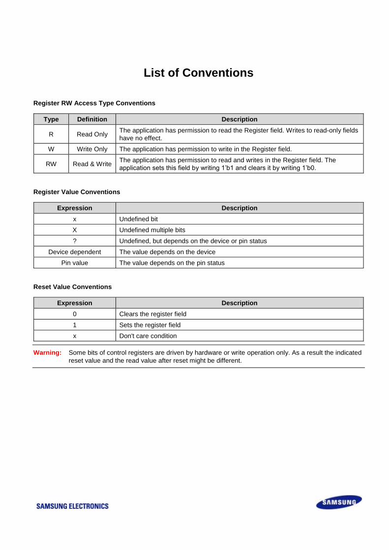
Register RW Access Type Conventions
Type Definition Description
R Read Only The application has permission to read the Register field. Writes to read-only fields
have no effect.
W Write Only The application has permission to write in the Register field.
RW Read & Write The application has permission to read and writes in the Register field. The
application sets this field by writing 1’b1 and clears it by writing 1’b0.
Register Value Conventions
Expression Description
x Undefined bit
X Undefined multiple bits
? Undefined, but depends on the device or pin status
Device dependent The value depends on the device
Pin value The value depends on the pin status
Reset Value Conventions
Expression Description
0 Clears the register field
1 Sets the register field
x Don't care condition
Warning: Some bits of control registers are driven by hardware or write operation only. As a result the indicated
reset value and the read value after reset might be different.
Samsung Confidential Exynos 5250_UM 1 Product Overview
1-1
1 Product Overview
1.1 Introduction
Exynos 5250 is a system-on-a-chip (SoC) based on the 32-bit RISC processor for tablets and cell-phones.
Designed with the 32 nm low power process, features of Exynos 5250 include:
Dual core CPU
Highest memory bandwidth
WQXGA display
1080p 60 frame video decoding and encoding hardware
3D graphics hardware
Image signal processor
High-speed interfaces such as eMMC4.5 and USB 3.0
Exynos 5250 uses the Cortex-A15 dual core, which is 40 % DMIPS higher than Cortex-A9 core and its speed is
1.7 GHz. It provides 12.8 GB/s memory bandwidth for heavy traffic operations such as 1080p video en/decoding,
3D graphics display and high resolution image signal processing with WQXGA display. The application processor
supports dynamic virtual address mapping, which helps software engineers to fully utilize the memory resources
with ease.
Exynos 5250 provides the best 3D graphics performance with wide range of APIs, such as OpenGL ES1.1, 2.0.
You can use Exynos 5250's 3D cores as GPGPUs supported by OpenCL full profile. Superior 3D performance
fully supports WQXGA display. Exynos 5250 supports not only low power eDP but also Panel-Self-Refresh (PSR)
to make a low power system. The native dual display, in particular, supports WQXGA resolution of a main LCD
display and 1080p 60 frame HDTV display throughout HDMI, simultaneously. Separate post processing pipeline
enables Exynos 5250 to make a real display scenario.
Exynos 5250 has integrated image signal processor (ISP). This ISP supports not only 8 mega pixel with 30 frames
per second throughput but also has special functionalities such as 3-dimensional noise reduction (3DNR), video
digital image stabilization (VDIS), and optical distortion compensation (ODC). The ISP helps to achieve zero-
shutter lag of camera shooting.
Samsung Confidential Exynos 5250_UM 1 Product Overview
1-2
Exynos 5250 lowers the Bill of Materials (BOM) by integrating these IPs:
DDR3/LPDDR3 interfaces
Image signal processor (ISP)
Eight channels of I2C for a variety of sensors
Variety of USB derivatives (USB Host or Device 3.0,USB Host or Device 2.0)
HSIC interfaces with PHY transceivers to connect with 802.11n, Ethernet, HSPA+, and 4G LTE modem
C2C for modem sharing DRAM
The application processor also supports eMMC 4.5 interfaces and EF-NAND3.0 to increase the file system’s
performance.
Exynos 5250 is available as FCFBGA Single Chip Package (SCP), which has a 0.45 mm ball pitch. Package on
Package (PoP) is also available with 0.4 mm ball pitch.
Samsung Confidential Exynos 5250_UM 1 Product Overview
1-3
1.2 Features
The key features of Exynos 5250 include:
Cortex-A15 dual core subsystem with 64/128-bit SIMD NEON
32 KB (Instruction)/32 KB (Data) L1 Cache and 1 MB L2 Cache
Core frequency of 1.7 GHz at overdrive/2.0 GHz by binning
128-bit Multi-layered bus architecture
Internal ROM and RAM for secure booting, security, and general purposes
Memory Subsystem:
Two ports 32-bit 800 MHz LPDDR3/DDR3 Interfaces
Or two ports 32-bit 533 MHz LPDDR2 Interfaces
Eight-bit ITU 601 camera interface
Multi-format Video Hardware Codec: 1080p 60fps (capable of decoding and encoding MPEG-4/H.263/H.264
and decoding only MPEG-2/VC1/VP8)
3D and 2D graphics hardware that supports OpenGL ES 1.1/2.0, OpenVG 1.1, and OpenCL 1.1 full profile
Image Signal Processor that supports BayerRGB up to 14-bit input with 16 MP 15 fps, 8 MP 30 fps through
MIPI CSI2 & YUV 8-bit interfaces and special functionalities such as 3-dimensional noise reduction (3DNR),
video digital image stabilization (VDIS), and optical distortion compensation (ODC)
JPEG Hardware Codec
LCD single display that supports max WQXGA (eDP)/WUXGA (MIPI DSI), 24 bpp RGB, YUV formats through
low power eDP and MIPI DSI
Native dual display that supports WQXGA single LCD display and 1080p HDMI simultaneously
HDMI 1.4 interfaces with on-chip PHY
One port YUV 8-bit interfaces for camera input
Two ports (4-lanes) MIPI CSI2 interfaces
One port (4-lanes) low power eDP
One port (4-lanes) MIPI DSI
USB 3.0 device or Host 1-channel that supports SS (5 Gbps) with on-chip PHY
USB 2.0 Host or Device 1-channel that supports LS/FS/HS (1.5 Mbps/12 Mbps/480 Mbps) with on-chip PHY
USB HSIC 2-channel that supports 480 Mbps with on-chip PHY
SATA 1.0/2.0/3.0 interface
One channel eMMC 4.5
One channel SDIO 3.0
Two channel SD 2.0
Two channel EF-NAND 3.0 interface
Four channel high-speed UART (up to 3 Mbps data rate for Bluetooth 2.1 EDR and IrDA 1.0 SIR)
Three channel high-speed SPI
Samsung Confidential Exynos 5250_UM 1 Product Overview
1-4
One channel AC-97, three channel PCM, and two channel 24-bit I2S audio interface that supports stereo
channel audio and one channel 24-bit I2S audio interface that supports 5.1 channel audio
One channel S/PDIF interface support for digital audio
Four channel I2C interface support (up to 400 kbps) for PMIC, HDMI, and general-purpose multi-masters
Four channel HS-I2C (up to 3.1 Mbps)
Samsung Reconfiguration Processor supports low power audio play
Cortex-A5 low power co-processor
MIPI HSI version 1.0 that supports 200 Mbps full-duplex
C2C that supports through path between DRAM and MODEM
Security subsystem that supports hardware crypto accelerators
32-channel DMA controllers
Configurable GPIOs
Real-time clock, PLLs, timer with PWM, multi-core timer, and watchdog timer
Samsung Confidential Exynos 5250_UM 1 Product Overview
1-5
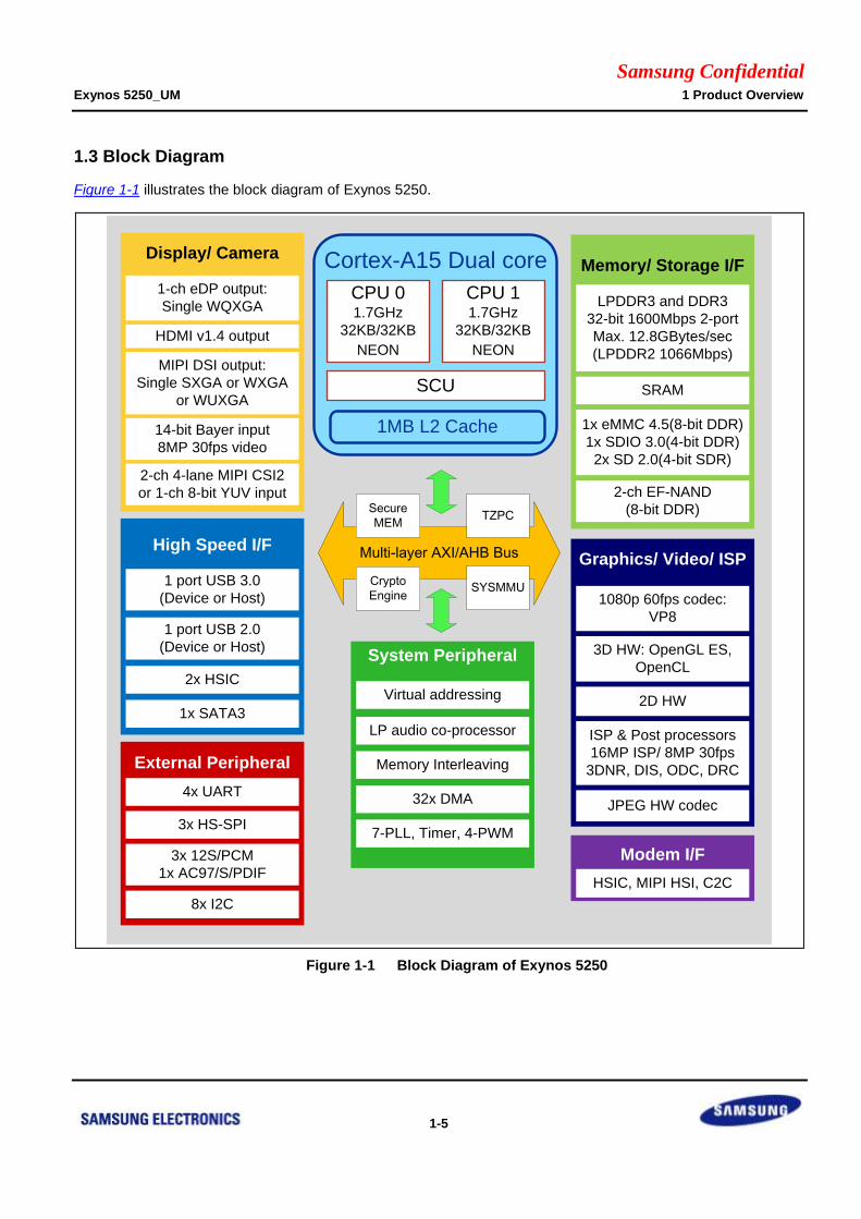
1.3 Block Diagram
Figure 1-1 illustrates the block diagram of Exynos 5250.
Memory/ Storage I/F
LPDDR3 and DDR3
32-bit 1600Mbps 2-port
Max. 12.8GBytes/sec
(LPDDR2 1066Mbps)
SRAM
1x eMMC 4.5(8-bit DDR)
1x SDIO 3.0(4-bit DDR)
2x SD 2.0(4-bit SDR)
2-ch EF-NAND
(8-bit DDR)
Graphics/ Video/ ISP
1080p 60fps codec:
VP8
3D HW: OpenGL ES,
OpenCL
2D HW
ISP & Post processors
16MP ISP/ 8MP 30fps
3DNR, DIS, ODC, DRC
JPEG HW codec
Modem I/F
HSIC, MIPI HSI, C2C
System Peripheral
Virtual addressing
LP audio co-processor
Memory Interleaving
32x DMA
7-PLL, Timer, 4-PWM
Display/ Camera
1-ch eDP output:
Single WQXGA
HDMI v1.4 output
2-ch 4-lane MIPI CSI2
or 1-ch 8-bit YUV input
14-bit Bayer input
8MP 30fps video
External Peripheral
4x UART
3x HS-SPI
8x I2C
3x 12S/PCM
1x AC97/S/PDIF
High Speed I/F
1 port USB 3.0
(Device or Host)
1 port USB 2.0
(Device or Host)
2x HSIC
1x SATA3
Multi-layer AXI/AHB Bus
Cortex-A15 Dual core
CPU 01.7GHz
32KB/32KB
NEON
CPU 11.7GHz
32KB/32KB
NEON
SCU
1MB L2 Cache
Secure
MEMTZPC
SYSMMUCrypto
Engine
MIPI DSI output:
Single SXGA or WXGA
or WUXGA
Figure 1-1 Block Diagram of Exynos 5250

Samsung Confidential Exynos 5250_UM 1 Product Overview
1-6
1.4 Product Details
This section includes:
ARM Core
Memory Subsystem
Display Subsystem
Camera and General Scaling Subsystem
Graphics, Multimedia Acceleration Hardware and Image Signal Processor
Security Subsystem
High Speed Interfaces
External Peripheral
Samsung Confidential Exynos 5250_UM 1 Product Overview
1-7
1.4.1 ARM Core
Exynos 5250 provides the latest ARM CPU core for high performance.
The ARM Cortex-A15 dual core processor uses ARMv7-A architecture with additional architecture extensions
for MP and virtualization.
Owing to its ability to reach 1.7 GHz in speed, the Cortex-A15 dual core processor can meet requirements for
performance-optimized consumer applications. It means 5,950 Dhrystone MIPS for each core (11,900 DMIPS
in total), which is 40 per cent more DMIPS/MHz than the Cortex-A9.
The key features of ARM Cortex-A15 Dual Core include:
Advanced bus interface for maximum throughput: Support for synchronous 1/n clock ratios to reduce the
latencies on high-speed processor designs (n: integer)
Advanced Single Instruction Multiple Data version 2 (SIMDv2) architecture extension for integer and
floating-point vector operations
ARM NEON Advanced SIMD Instruction: Supports 64/128-bit registers with 8/16/32-bit Integer data and
32-bit FP data formats and enlarging 32 double precision registers
High performance single or 16 double precision (D16) Floating Point Unit with VFPv4 architecture:
Compatible with the IEEE 754 standard, VFPv2 (Cortex-A8), and VFP11 (ARM11)
Security extensions for enhanced security
Virtualization extensions for development of virtualized systems that enables switching of guest operating
systems
Multi-Processing extensions for multiprocessing functionality
Multi-core ARM TrustZone technology with interrupt virtualization
ARM Generic Timer with 64-bit counter/timer and support for Virtualization Extensions (A15)
Program Trace Macrocell (PTM) based on the Program Flow Trace (PFT) v1.1 architecture
ARMv7.1 Debug architecture that includes support for Security Extensions and CoreSight
Samsung Confidential Exynos 5250_UM 1 Product Overview
1-8
1.4.2 Memory Subsystem
Exynos 5250 provides the leading memory bandwidth for mobile applications.
Mobile DDR3 (LPDDR3) Interface
Two ports x32 data bus with 800 MHz per pin, double data rate (DDR)
1.2 V interface voltage
Density: Maximum 4 GB by memory map limit, Recommend: Maximum 2 memory dice per port.
NOTE: The max number of column address bits is 10.
Mobile DDR2 (LPDDR2) interface
Two ports x32 data bus with 533 MHz per pin and double data rate (DDR)
1.2 V interface voltage
Density: Maximum 4 GB by memory map limit, Recommend: Maximum 2 memory dice per port.
NOTE: The max number of column address bits is 10.
DDR3/DDR3L Interface
Two ports x32 data bus with 800 MHz per pin and double data rate (DDR)
1.5 V/1.35 V interface voltage
Density: Maximum 4 GB by memory map limit, Recommend: Maximum 2 memory dice per port.
NOTE: The max number of column address bits is 10.
eMMC and SD card interface
One channel 8-bit eMMC4.5 (1.8 V only)
One channel 4-bit SD3.0 (1.8 V only)
Two channel eMMC4.3/SD2.0 3.3 V/1.8 V interface voltage
EF-NAND3.0 interface
Two ports x8-bit data bus with up to 200 MHz per pin and double data rate (DDR)
Embedded internal ROM booting: The system does not need a booting device
Samsung Confidential Exynos 5250_UM 1 Product Overview
1-9
1.4.3 Display Subsystem
This section includes:
LCD Controller
eDisplayPort Interface
Digital TV Display
MIPI DSI Interface
1.4.3.1 LCD Controller
Maximum resolution up to WQXGA (2560 1600)
Virtual screen size up to 16 MB pixels
Supports transparent overlay and real-time overlay plane multiplexing
Supports color key and simultaneous blend dual operations
Soft Scrolling: Horizontal one byte resolution and vertical one pixel resolution
Source Format:
Windows 0, 1, 2, 3 and 4
o Supports 1, 2, 4, or 8-bpp (bits per pixel) palletized color
o Supports 8, 16, 18, or 24-bpp non-palletized color
o Supports RGB (8:8:8)
Palettes and Look-up tables
Five 256 32-bit (αRGB8888) palettes for windows 0 to 4
8-bit alpha blending
Bus Interface: 64-bit AMBA AXI master and 32-bit AMBA AHB slave
Supports 3D stereoscopic display
Samsung Confidential Exynos 5250_UM 1 Product Overview
1-10
1.4.3.2 eDisplayPort (eDP) Interface
Compliant with DisplayPortTM
Specification, Version 1.1a.
Main link containing four physical lanes of 2.7/1.62 Gbps/lane
Bi-directional auxiliary link with up to one Mbps speed
Video Format: RGB 24bpp
Video slave mode
APB slave bus interface
Hot plug and unplug detection and link status monitor
Support VESA DMT and CVT timing standards
Built-in video BIST patterns
Specially designed low power PHY for mobile
1.4.3.3 Digital TV Display
High Definition Multimedia Interface (HDMI) 1.4 compliant (with 3D)
Single-cable digital audio/video connection with a maximum bit rate of 4.46 Gbps
Supports 5.1-channel/96 KHz/24-bit audio
Supports 24-bit (RGB or YCbCr) color depth
Supports 480p, 576p, 720p, and 1080i/p
Supports HDMI stereoscopy
1.4.3.4 MIPI DSI Interface
MIPI DSI Master v1.01_R11 (default) and r03 compliant
One port MIPI D-PHY v1.0: Four lanes, linked with MIPI DSI master
Tx bandwidth in high-speed mode: 80 Mbps to 920 Mbps per 1-lane
One data command bi-directional FIFO
Input format: RGB 24 bpp only
Output format: RGB 24 bpp
Maximum resolution: 1920 1200 (WUXGA)
Samsung Confidential Exynos 5250_UM 1 Product Overview
1-11
1.4.4 Camera and General Scaling Subsystem
This section includes:
Camera Interface
General Scaler
MIPI CSI Interface
1.4.4.1 Camera Interface
ITU-R BT 601 compliant
8-bit YCbCr422 input
MIPI CSI-2 Standard Specification v1.01r06 compliant with YUV, RGB, and Bayer Raw format input
One ITU camera input support and format: YCbCr422 or Bayer RAW 8/10/12/14-bit
Two MIPI CSI camera input support and format: YCbCr422 or Bayer RAW 8/10/12/14-bit
1.4.4.2 General Scaler
DMA input and output support and format
YCbCr420: Two planes (Including tile) and three planes
YCbCr422: one plane, two planes
RGB888/RGB565
Maximum input resolution support
2048 2048 for Tile Mode or Rotation
4800 3344 for Other Cases
Built-in enhanced Color Space Conversion (CSC) engine
Input or Output image mirroring and rotation: 90°/180°/270° Rotation and X-Flip/Y-Flip
Scaling Algorithm: Vertical 4 taps/16 poly-phase filter, horizontal 8 taps/16 poly-phase filter
4 circular frame buffer support for DMA Read part
16 circular frame buffer support for DMA Write part
Supporting two local-out paths, which are FIMD1/MIXER.
Supporting two local-in paths, which are Camera/FIMD1.
Samsung Confidential Exynos 5250_UM 1 Product Overview
1-12
1.4.4.3 MIPI CSI Interface
MIPI CSI-2 Standard Specification v1.01r06 compliant
Two ports MIPI D-PHY v1.0: each port has 4-lanes, linked with MIPI CSI-2 slave
Rx bandwidth in high-speed mode: 80 Mbps to 920 Mbps per lane
Input formats
YUV422-8bit format
Bayer Raw 8/10/12/14 and Embedded 8-bit based packets
User-defined packets (for example, JPEG)
Output: 32-bit bus-width for parallel output
Three clock domains for SFR configuration, BYTECLK, and pixel clock assignment for ISP or camera
Samsung Confidential Exynos 5250_UM 1 Product Overview
1-13
1.4.5 Graphics, Multimedia Acceleration Hardware and Image Signal Processor
This section includes:
3D Hardware Graphic Accelerator
2D Hardware Graphic Accelerator
Hardware Rotator
JPEG Hardware Codec
Multi Format Video Hardware Codec
Audio Subsystem
Image Signal Processor (ISP) Sub System
1.4.5.1 3D Hardware Graphic Accelerator
A rich API feature set
An effective core for General Purpose GPU (GPGPU) applications
Leading memory bandwidth and power consumption for 3D graphics content
Scalability for products from smart phones to high-end mobile computing
Performance leading 3D graphics
Leading image quality with FP64 and anti-aliasing
Ease of integration, latency tolerance, and standard hardware interfaces
Versatile power management strategy, which you can tune to give the best power and performance
combination for applications. Each core is individually power managed
1.4.5.2 2D Hardware Graphic Accelerator
BitBLT:
Stretched BitBLT support using scale factor: Nearest sampling, smooth scaling (Bilinear sampling)
Memory-to-Memory BitBLT
Reverse Addressing: X Positive/Negative, Y Positive/Negative
Various repeat type support: Repeat, Reflect, Pad, Clamp, and None
Per-pixel Operation
Maximum 8000 8000 image size
Window clipping
90°/180°/270° Rotation and X-Flip/Y-Flip
Four operand Raster Operation (ROP4)
Alpha Blending: User-specified constant alpha value or per-pixel alpha value, Porter/Duff Rule support
Color Key: RGBA Color Key, YCbCr Color Key
Dithering
4 Pixel Pipeline
Data Format: 8/16/24/32-bpp, Packed 24-bpp Input/Output Color Format, and YCbCr format support
Samsung Confidential Exynos 5250_UM 1 Product Overview
1-14
1.4.5.3 Hardware Rotator
Supported image format: YCbCr422 (Interleave), YCbCr420 (non-interleave), RGB565,
and RGB888 (unpacked)
Supported rotate degree: 90, 180, 270, flip vertical, and flip horizontal
1.4.5.4 JPEG Hardware Codec
Encoding input format: YCbCr4:4:4, YCbCr4:2:2, YCbCr4:2:0, RGB888, RGB565, or Gray
1.4.5.5 Multi Format Video Hardware Codec
Full HD 60 fps capable of time-multiplexed, multi-stream, and multi-format encoding and decoding hardware
H.264 1080p 60 fps decoding: BP @ L4.2, MP @ L4.2, HP @ L4.2
H.264 1080p 60 fps encoding: BP @ L4.2, MP @ L4.2, HP @ L4.2
H.263 D1 30 fps decoding: Profile 3, Annex-I/J/K/T/D/F (except OBMC) support
H.263 D1 30 fps encoding: Baseline Profile
MPEG-4 1080p 30 fps decoding: SP, ASP @ L5, Xvid support
MPEG-4 1080p 30 fps encoding: SP, ASP @ L5
VC-1 1080p 30 fps decoding only: SP @ ML, MP @ HL, AP @ L3
and WMV-9 conformant stream (except CP)
VP8 1080p 60fps decoding: Version0/1/2/3
MPEG-2 1080p 30 fps decoding only: MP @ HL and MPEG-1 support (except D-picture)
Encoder common features
[ 256, 256] ½ and ¼ -pel accuracy motion estimation
B-picture support (number of B-pictures: 1 or 2)
16 16, 16 8, 8 16, and 8 8 block size support in H.264
Spatial mode of direct mode support in H.264
4 MV and unrestricted motion vector support in MPEG-4
Rate control support (Variable Bit-Rate and Constant Bit-Rate)
Cyclic intra refresh support
Decoder common features
Provides range mapping information for post-processing in VC-1
One warp point GMC support in MPEG-4
De-blocking filter for post-processing in MPEG-4
Error detection and concealment
Error resilience tool (re-sync marker and data partitioning with RVLC) support in MPEG-4
Video telephony (H.263) support up to D1 30 fps
Samsung Confidential Exynos 5250_UM 1 Product Overview
1-15
1.4.5.6 Audio Subsystem
Low power audio subsystem
5.1 channel I2S with 32-bit width 64-depth FIFO
Hardware mixer mixes primary and secondary sounds
1.4.5.7 Image Signal Processor (ISP) Sub System
Imaging subsystem to process image signal from an image sensor
Dedicated processor for controlling many sub-IPs: Cortex-A5 with Neon, 16 K I-Cache and 16 K D-Cache
Supported image resolution: 4808 3356 @ 15 fps, Full-HD @ 60 fps
Image processing
Demosaic
Denoise
Dynamic range compression
Image resizing
Optical distortion correction
Digital image stabilization: available only for less than full-HD
Inter-frame noise reduction
Face detection
System control feature
Interrupt controller of Cortex-A5
Watch Dog timer
Controller communicates with main host processor
Peripherals for sensor module control
Multi-PWM 6 channel
I2C 3 channel
SPI 2 channel
ADC 4 channel for motor control
UART for debugging
18 GPIO
Debugging system
Coresight for multi-core co-debugging

Samsung Confidential Exynos 5250_UM 1 Product Overview
1-16
1.4.6 Security Subsystem
Exynos 5250 provides hardware engines and memories for security.
On-chip secure boot ROM: 64 KB ROM for secure boot
On-chip secure RAM: 352 KB secure RAM for security function
Hardware Crypto Accelerators: AES, DES/3DES, ARC4, SHA-1/SHA-256/MD5/HMAC/PRNG, TRNG, PKA,
and Secure Key Manager
e-Fuse:
128-bit root key
112-bit Chip ID
24-bit Thermal Sensor
RTIC (Run-Time Integrity Check): Memory data integrity check during run-time.
Monotonic Counter: incremental counter for secure contents
Samsung Confidential Exynos 5250_UM 1 Product Overview
1-17
1.4.7 High Speed Interfaces
This section includes:
USB DRD (Dual Role Device) 3.0 Interface
USB Host 2.0 Interface
USB Device 2.0 Interface
USB HSIC 1.0 Interface
SATA 3.0 Interface
1.4.7.1 USB DRD (Dual Role Device) 3.0 Interface
Both USB Device 3.0 and USB Device 2.0 compliant
Both USB HOST 3.0 and USB HOST 2.0 compliant
Supports both USB Device 3.0 interface and USB Device 2.0 interface
Supports both USB Host 3.0 interface and USB Host 2.0 interface
Supports full-speed (12 Mbps) and high-speed (480 Mbps) modes with USB Device 2.0 interface
Supports super-speed (5 Gbps) mode with USB Device 3.0 interface
Supports one USB port (you can use USB 3.0 or USB 2.0 at a time)
On-chip USB PHY transceiver
Supports flexible endpoint configuration
Supports up to 16 bidirectional endpoints, including control endpoint 0
1.4.7.2 USB Host 2.0 Interface
USB Host 2.0 compliant
Supports low-speed (1.5 Mbps), full-speed (12 Mbps), and high-speed (480 Mbps) modes
Supports one USB Host port
On-chip USB PHY transceiver
Supports EHCI asynchronous schedule park capability
Supports EHCI programmable frame list flag
Samsung Confidential Exynos 5250_UM 1 Product Overview
1-18
1.4.7.3 USB Device 2.0 Interface
USB Device 2.0 compliant
Supports low-speed (1.5 Mbps), full-speed (12 Mbps), and high-speed (480 Mbps) modes
Supports one USB device port. (muxed with USB2.0 Host)
One Control Endpoint 0 for control transfer
15 Device Mode programmable Endpoints
1.4.7.4 USB HSIC 1.0 Interface
USB HSIC 1.0 compliant
Supports 480 Mbps
Supports two HSIC ports
On-chip USB PHY transceiver
HSIC enable/disable control setting
1.4.7.5 SATA 3.0 Interface
Supports SATA 1.0/2.0/3.0 interface
Supports one AHCI port
On-chip SATA PHY transceiver
Supports 1.5/3.0/6.0 Gbps
Support Spread Spectrum Clocking in SATA PHY transceiver
Samsung Confidential Exynos 5250_UM 1 Product Overview
1-19
1.4.8 External Peripheral
This section includes:
eMMC and SD Interface
UART Interface
UART Interface in ISP
SPI Interface
SPI Interface in ISP
I2S Bus Interface
PCM Audio Interface
AC97 Audio Interface
S/PDIF Interface
I2C Bus Interface
HS-I2C
Configurable GPIOs
Global A/D Converter
1.4.8.1 eMMC and SD Interface
Multimedia Card Protocol version 4.5 compatible (eMMC)
Secure Digital I/O (SDIO-Version 3.0)
Secure Digital Memory (SD mem-Version 2.0)
Pin configuration: 1-channel 8-bit eMMC4.5 and 1-channel SDIO3.0 and 2-channel 4-bit eMMC4.3/SD2.0
DMA-based or Interrupt-based operation
512 bytes FIFO for Tx/Rx
1.4.8.2 UART Interface
Four-port high-speed UART with DMA-based or interrupt-based operation
UART FIFO: 256 bytes 1-port, 64 bytes 2-port, and 16 bytes 2-port
Supports 5-bit, 6-bit, 7-bit, or 8-bit serial data transmit and receive
Programmable baud rate
Supports IrDA 1.0 SIR (115.2 Kbps) mode
Loop back mode for testing
Non-integer clock divide in Baud clock generation (BRM)
Samsung Confidential Exynos 5250_UM 1 Product Overview
1-20
1.4.8.3 UART Interface in ISP
One-port high-speed UART with DMA-based or interrupt-based operation
UART FIFO: 64 bytes one-port
Supports 5-bit, 6-bit, 7-bit, or 8-bit serial data transmit and receive
Programmable baud rate
Supports IrDA 1.0 SIR (115.2 Kbps) mode
Loop back mode for testing
Non-integer clock divide in Baud clock generation (BRM)
1.4.8.4 SPI Interface
Three-channel Serial Peripheral Interface
Up to 50 Mbps full duplex
SPI FIFO: 256 bytes 1-port, 64 bytes 2-port
DMA-based or interrupt-based operation
1.4.8.5 SPI Interface in ISP
Two-channel Serial Peripheral Interface
Up to 50 Mbps full duplex
SPI FIFO: 256 bytes 2-port
DMA-based or interrupt-based operation
1.4.8.6 I2S Bus Interface
Three-channel I2S for audio codec interface with DMA-based operation
Serial, 8/16/20/24-bit per channel data transfers
Supports I2S, MSB-justified, and LSB-justified data formats
Supports 5.1 channel (1-channel)
Various bit clock frequency and codec clock frequency support
16, 24, 32, 48, 64 fs of bit clock frequency
256, 384, 512, 768 fs of codec clock frequency

Samsung Confidential Exynos 5250_UM 1 Product Overview
1-21
1.4.8.7 PCM Audio Interface
16-bit mono audio interface
Master mode only
1.4.8.8 AC97 Audio Interface
Independent channels for stereo PCM In, stereo PCM Out, and mono MIC In
16-bit stereo (2-channel) audio
Variable sampling rate AC97 Codec interface (48 KHz and below)
Supports AC97 Full Specification
1.4.8.9 S/PDIF Interface
Linear PCM up to 24-bit per sample support
Non-linear PCM formats such as AC3, MPEG1, and MPEG2 support
2x24-bit buffers that are alternately filled with data
1.4.8.10 I2C Bus Interface
Four-channel Multi-Master I2C
Serial, 8-bit oriented, and bi-directional data transfers (up to 100K-bit/s in the standard mode)
Up to 400K-bit/s in the fast mode
Samsung Confidential Exynos 5250_UM 1 Product Overview
1-22
1.4.8.11 HS-I2C
Support four channel high speed I2C mode (up to 3.1 Mbps)
Supports operation based on DMA or interrupt
Transmits and receives data separately
Supports non-integer clock division
Operates in two modes: Master and slave
1.4.8.12 Configurable GPIOs
Controls 205 External Interrupts
Controls 32 External Wake-up Interrupts
253 multi-functional input/output ports
Controls pin states in Sleep Mode, except GPX0, GPX1, GPX2, and GPX3 (GPX0/1/2/3 pins are alive-pads)
1.4.8.13 Global A/D Converter
Eight-channel multiplexed 12-bit resolution ADC
Maximum 1M samples/sec with 5 MHz clock
Samsung Confidential Exynos 5250_UM 1 Product Overview
1-23
1.4.9 Modem Interfaces
This section includes:
HSIC
MIPI HSI
C2C
1.4.9.1 HSIC
USB HSIC 1.0 compliant
Supports two HSIC ports
Supports 480 Mbps with half duplex transfer
Supports maximum 10 Cm trace length
1.4.9.2 MIPI HSI
Compliant to HSI specification version 1.0
Full-Duplex High Speed Serial Interface
Supports eight-logical channels for both transmit and receive operations
Maximum bandwidth of 200 Mbs in both transmit and receive directions
1.4.9.3 C2C
Two DDR clock signals per direction for TX and RX paths
Scalable up to 16-bit inputs/16-bit outputs
Support for two different PHY voltages: 1.2 V and 1.8 V
Bit rates/signal: Up to 400 Mb/s per TX output signals and 400 Mb/s per RX input signals
Protocol supports In Band Flow Control without extra pins
Supports multiple outstanding transactions Reads, Writes and Interrupts
Provides signals for system to manage power management
Actively controls serial clock for power management
Samsung Confidential Exynos 5250_UM 1 Product Overview
1-24
1.4.10 Low Power Co-Processor
This section includes:
Samsung Reconfigurable Processor
Cortex-A5
1.4.10.1 Samsung Reconfigurable Processor
Low power and ultra low power audio mode
1.4.10.2 Cortex-A5
Low power co-processor unit
ARM Cortex-A5 core processor uses ARMv7-A architecture
16 KB instruction cache and 16 KB data cache
Samsung Confidential Exynos 5250_UM 1 Product Overview
1-25
1.4.11 System Peripheral
This section includes:
Real Time Clock
PLL
Timer with Pulse Width Modulation
Multi-Core Timer
16-bit Watch Dog Timer
DMA
Generic Interrupt Controller
Power Management
1.4.11.1 Real Time Clock
Full clock features: Second, minute, hour, date, day, week, month, and year
32.768 kHz operation
Alarm interrupt
Time-tick interrupt
1.4.11.2 PLL
Seven on-chip PLLs: APLL, MPLL, BPLL, CPLL, GPLL, EPLL, VPLL (dithered PLL)
APLL generates clock for ARM core
MPLL generates system bus clock for memory controller
BPLL generates Graphic 3D processor clock and 1066 MHz clock for memory controller if necessary
CPLL generates the clock for Multi Format Video Hardware Codec
GPLL generates the clock for Graphic 3D processor or other clocks for DVFS flexibility
EPLL generates the clocks for audio interface and other external device interfaces
VPLL generates the dithered PLL and helps to reduce the EMI of display and camera

Samsung Confidential Exynos 5250_UM 1 Product Overview
1-26
1.4.11.3 Timer with Pulse Width Modulation
Four channel 32-bit timer with PWM
One channel 32-bit internal timer with DMA-based or interrupt-based operation
Programmable duty cycle, frequency, and polarity
Dead-zone generation
Supports external clock source
1.4.11.4 Multi-Core Timer
Two private timers
A 32-bit counter that generates an interrupt when it reaches zero
Configurable single-shot or auto-reload modes
Configurable starting values for the counter
A global timer
A 64-bit incrementing counter with an auto-incrementing feature
Accessible to all Cortex-A15 processor
1.4.11.5 16-bit Watch Dog Timer
Supports normal interval timer mode with interrupt request
Activates internal reset signal if the timer count value reaches 0 (time-out).
Supports level-triggered interrupt mechanism
1.4.11.6 DMA
MDMA0/MDMA1
Eight channels simultaneously for each MDMA
Burst transfer mode to enhance transfer rate
PDMA
16 channels simultaneously
16 channel IO to memory, memory to IO, and IO to IO support
Burst transfer mode to enhance the transfer rate
Samsung Confidential Exynos 5250_UM 1 Product Overview
1-27
1.4.11.7 Generic Interrupt Controller
AXI slave interface for CPU interface and distributor
Supports two cores such as Cortex-A15 core and Cortex-A5
Supports the ARM architecture Virtualization Extension
Supports the ARM architecture Security Extensions
1.4.11.8 Power Management
Clock-off control for individual components
Various power-down modes are available, such as Idle, Deep Idle, Stop, Deep Stop, and Sleep modes
Wake-up by one of the external interrupts or by the RTC alarm interrupt
Samsung Confidential Exynos 5250_UM 1 Product Overview
1-28
1.4.12 Electrical Characteristics
This section includes:
Operational ARM Core Frequency
Operating Voltage
Operating Temperature
1.4.12.1 Operational ARM Core Frequency
1.35 GHz @ 1.1 V/1.7 GHz @ max 1.3 V
1.4.12.2 Operating Voltage
Supply voltage for logic core: 1.0 V
External Memory interface: 1.2 V/1.35 V/1.5 V/1.8 V
External I/O interface: 1.2 V to 3.3 V
Analog voltage: 1.2 V/1.8 V/3.3 V
Samsung Confidential Exynos 5250_Use'r Manual_REV1.00 (Preliminary Spec) 1 Product Overview
1-29
1.4.13 Package Information
This section includes:
Single Chip Package
Package on Package
1.4.13.1 Single Chip Package
15 mm 16 mm, 0.45 mm ball pitch
1.4.13.2 Package on Package
14 mm 14 mm, 0.4 mm ball pitch
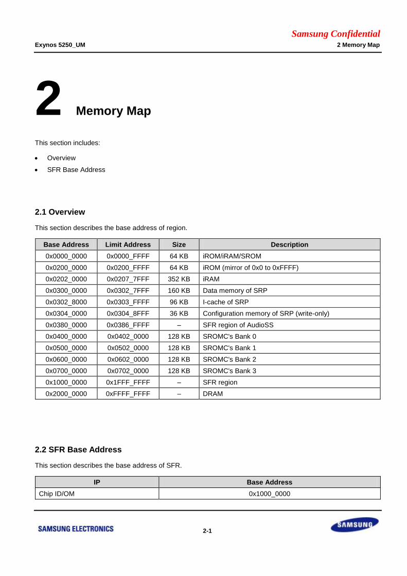
Samsung Confidential Exynos 5250_UM 2 Memory Map
2-1
2 Memory Map
This section includes:
Overview
SFR Base Address
2.1 Overview
This section describes the base address of region.
Base Address Limit Address Size Description
0x0000_0000 0x0000_FFFF 64 KB iROM/iRAM/SROM
0x0200_0000 0x0200_FFFF 64 KB iROM (mirror of 0x0 to 0xFFFF)
0x0202_0000 0x0207_7FFF 352 KB iRAM
0x0300_0000 0x0302_7FFF 160 KB Data memory of SRP
0x0302_8000 0x0303_FFFF 96 KB I-cache of SRP
0x0304_0000 0x0304_8FFF 36 KB Configuration memory of SRP (write-only)
0x0380_0000 0x0386_FFFF – SFR region of AudioSS
0x0400_0000 0x0402_0000 128 KB SROMC's Bank 0
0x0500_0000 0x0502_0000 128 KB SROMC's Bank 1
0x0600_0000 0x0602_0000 128 KB SROMC's Bank 2
0x0700_0000 0x0702_0000 128 KB SROMC's Bank 3
0x1000_0000 0x1FFF_FFFF – SFR region
0x2000_0000 0xFFFF_FFFF – DRAM
2.2 SFR Base Address
This section describes the base address of SFR.
IP Base Address
Chip ID/OM 0x1000_0000
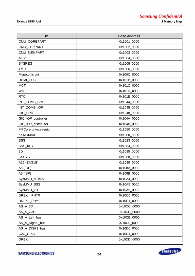
Samsung Confidential Exynos 5250_UM 2 Memory Map
2-2
IP Base Address
CMU_COREPART 0x1001_0000
CMU_TOPPART 0x1002_0000
CMU_MEMPART 0x1003_0000
ALIVE 0x1004_0000
SYSREG 0x1005_0000
TMU 0x1006_0000
Monotonic cnt 0x100C_0000
HDMI_CEC 0x101B_0000
MCT 0x101C_0000
WDT 0x101D_0000
RTC 0x101E_0000
INT_COMB_CPU 0x1044_0000
INT_COMB_IOP 0x1045_0000
GIC_CPU 0x1048_0000
GIC_IOP_controller 0x104A_0000
GIC_IOP_distributor 0x104B_0000
MPCore private region 0x1050_0000
ns MDMA0 0x1080_0000
SSS 0x1083_0000
SSS_KEY 0x1084_0000
2D 0x1085_0000
CSSYS 0x1088_0000
A15 (EAGLE) 0x1089_0000
A5 (IOP) 0x108A_0000
A5 (ISP) 0x108B_0000
SysMMU_MDMA 0x10A4_0000
SysMMU_SSS 0x10A5_0000
SysMMU_2D 0x10A6_0000
DREXII_PHY0 0x10C0_0000
DREXII_PHY1 0x10C1_0000
AS_A_3D 0x10CC_0000
AS_A_C2C 0x10CD_0000
AS_A_Left_bus 0x10CE_0000
AS_A_Right0_bus 0x10CF_0000
AS_A_DISP1_bus 0x10D0_0000
C2C_GPIO 0x10D1_0000
DREXII 0x10DD_0000
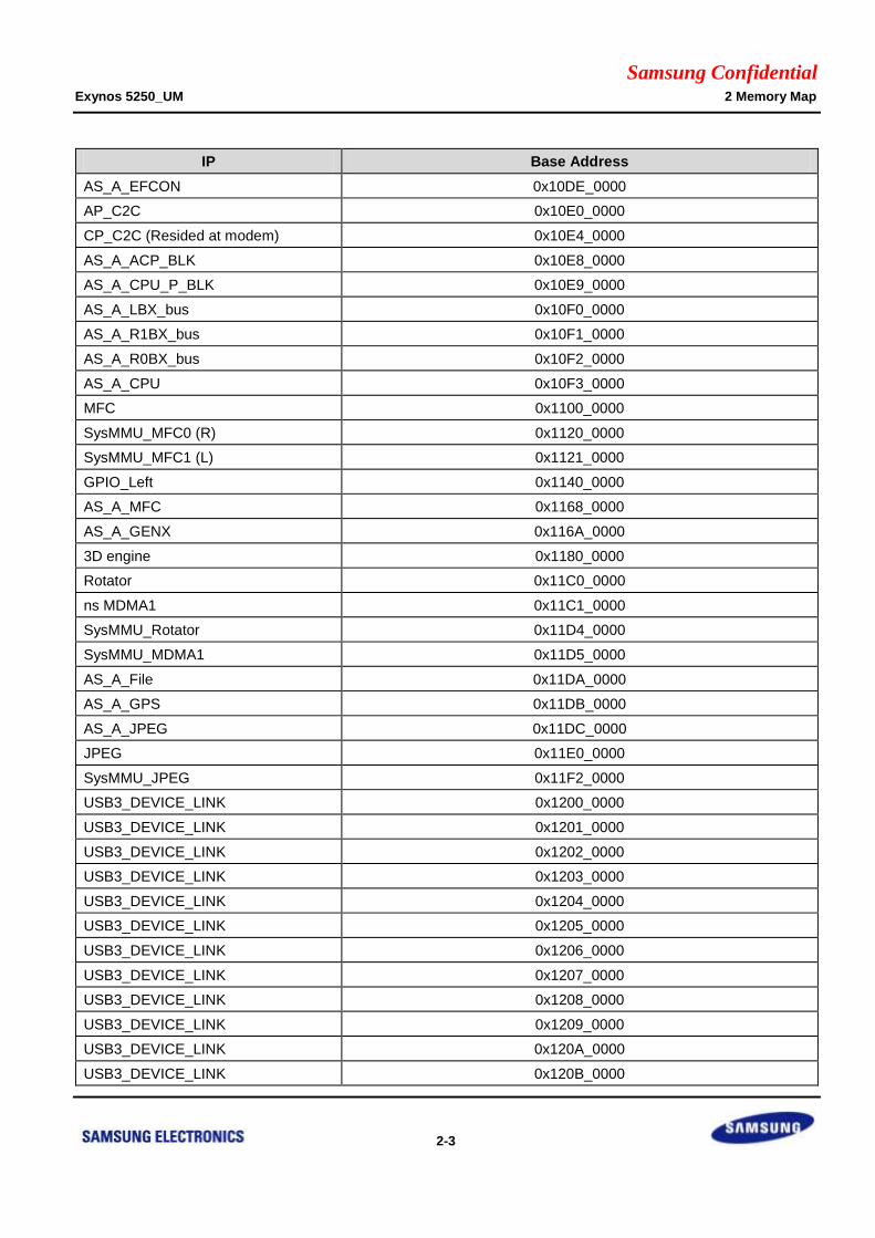
Samsung Confidential Exynos 5250_UM 2 Memory Map
2-3
IP Base Address
AS_A_EFCON 0x10DE_0000
AP_C2C 0x10E0_0000
CP_C2C (Resided at modem) 0x10E4_0000
AS_A_ACP_BLK 0x10E8_0000
AS_A_CPU_P_BLK 0x10E9_0000
AS_A_LBX_bus 0x10F0_0000
AS_A_R1BX_bus 0x10F1_0000
AS_A_R0BX_bus 0x10F2_0000
AS_A_CPU 0x10F3_0000
MFC 0x1100_0000
SysMMU_MFC0 (R) 0x1120_0000
SysMMU_MFC1 (L) 0x1121_0000
GPIO_Left 0x1140_0000
AS_A_MFC 0x1168_0000
AS_A_GENX 0x116A_0000
3D engine 0x1180_0000
Rotator 0x11C0_0000
ns MDMA1 0x11C1_0000
SysMMU_Rotator 0x11D4_0000
SysMMU_MDMA1 0x11D5_0000
AS_A_File 0x11DA_0000
AS_A_GPS 0x11DB_0000
AS_A_JPEG 0x11DC_0000
JPEG 0x11E0_0000
SysMMU_JPEG 0x11F2_0000
USB3_DEVICE_LINK 0x1200_0000
USB3_DEVICE_LINK 0x1201_0000
USB3_DEVICE_LINK 0x1202_0000
USB3_DEVICE_LINK 0x1203_0000
USB3_DEVICE_LINK 0x1204_0000
USB3_DEVICE_LINK 0x1205_0000
USB3_DEVICE_LINK 0x1206_0000
USB3_DEVICE_LINK 0x1207_0000
USB3_DEVICE_LINK 0x1208_0000
USB3_DEVICE_LINK 0x1209_0000
USB3_DEVICE_LINK 0x120A_0000
USB3_DEVICE_LINK 0x120B_0000
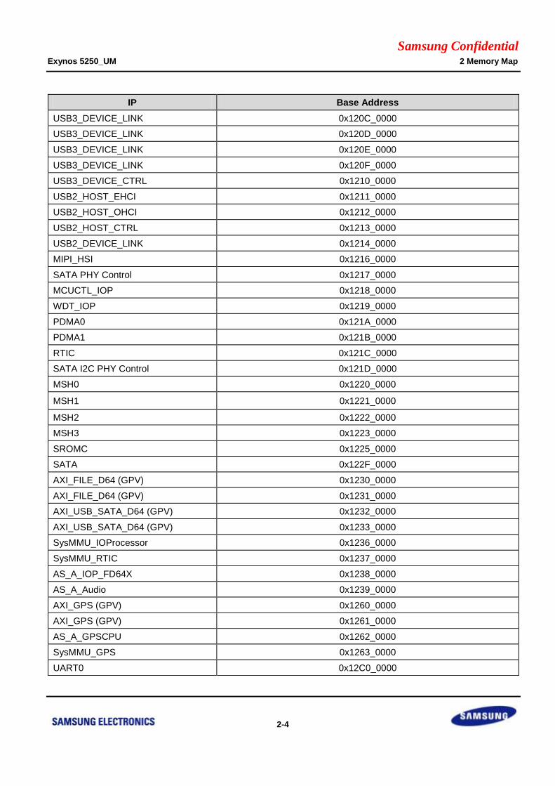
Samsung Confidential Exynos 5250_UM 2 Memory Map
2-4
IP Base Address
USB3_DEVICE_LINK 0x120C_0000
USB3_DEVICE_LINK 0x120D_0000
USB3_DEVICE_LINK 0x120E_0000
USB3_DEVICE_LINK 0x120F_0000
USB3_DEVICE_CTRL 0x1210_0000
USB2_HOST_EHCI 0x1211_0000
USB2_HOST_OHCI 0x1212_0000
USB2_HOST_CTRL 0x1213_0000
USB2_DEVICE_LINK 0x1214_0000
MIPI_HSI 0x1216_0000
SATA PHY Control 0x1217_0000
MCUCTL_IOP 0x1218_0000
WDT_IOP 0x1219_0000
PDMA0 0x121A_0000
PDMA1 0x121B_0000
RTIC 0x121C_0000
SATA I2C PHY Control 0x121D_0000
MSH0 0x1220_0000
MSH1 0x1221_0000
MSH2 0x1222_0000
MSH3 0x1223_0000
SROMC 0x1225_0000
SATA 0x122F_0000
AXI_FILE_D64 (GPV) 0x1230_0000
AXI_FILE_D64 (GPV) 0x1231_0000
AXI_USB_SATA_D64 (GPV) 0x1232_0000
AXI_USB_SATA_D64 (GPV) 0x1233_0000
SysMMU_IOProcessor 0x1236_0000
SysMMU_RTIC 0x1237_0000
AS_A_IOP_FD64X 0x1238_0000
AS_A_Audio 0x1239_0000
AXI_GPS (GPV) 0x1260_0000
AXI_GPS (GPV) 0x1261_0000
AS_A_GPSCPU 0x1262_0000
SysMMU_GPS 0x1263_0000
UART0 0x12C0_0000

Samsung Confidential Exynos 5250_UM 2 Memory Map
2-5
IP Base Address
UART1 0x12C1_0000
UART2 0x12C2_0000
UART3 0x12C3_0000
USI0 0x12C5_0000
I2C0 0x12C6_0000
I2C1 0x12C7_0000
I2C2 0x12C8_0000
I2C3 0x12C9_0000
I2C4 0x12CA_0000
I2C5 0x12CB_0000
I2C6 0x12CC_0000
I2C7 0x12CD_0000
I2C_HDMI 0x12CE_0000
USI1 0x12D0_0000
TSADC 0x12D1_0000
SPI0 0x12D2_0000
SPI1 0x12D3_0000
SPI2 0x12D4_0000
USI2 0x12D5_0000
I2S1 0x12D6_0000
I2S2 0x12D7_0000
PCM1 0x12D8_0000
PCM2 0x12D9_0000
AC97 0x12DA_0000
SPDIF 0x12DB_0000
PWM 0x12DD_0000
USI3 0x12DE_0000
FIMC_ISP 0x1300_0000
FIMC_DRC_TOP 0x1301_0000
FIMC_SCALERC 0x1302_0000
FIMC_SCALERP 0x1303_0000
FIMC_FD_TOP 0x1304_0000
FIMC_ODC 0x1305_0000
FIMC_DIS 0x1306_0000
FIMC_3DNR 0x1307_0000
ASYNC_AXI_M 0x130F_0000
MPWM_ISP 0x1311_0000
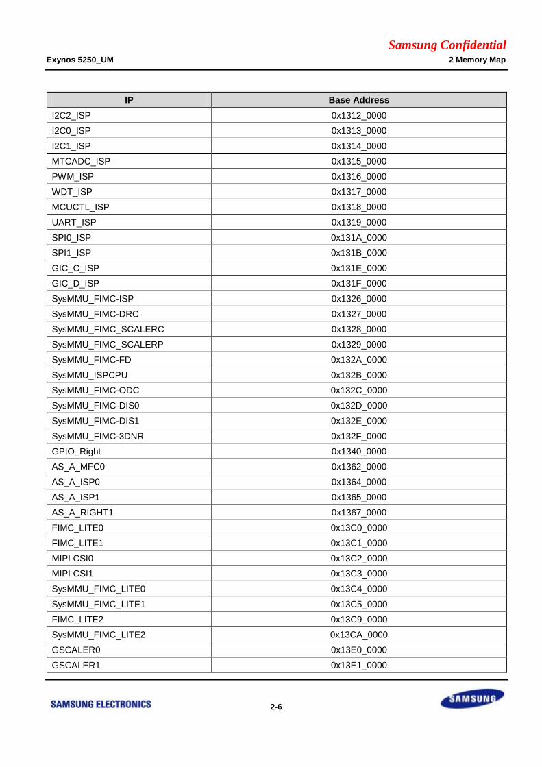
Samsung Confidential Exynos 5250_UM 2 Memory Map
2-6
IP Base Address
I2C2_ISP 0x1312_0000
I2C0_ISP 0x1313_0000
I2C1_ISP 0x1314_0000
MTCADC_ISP 0x1315_0000
PWM_ISP 0x1316_0000
WDT_ISP 0x1317_0000
MCUCTL_ISP 0x1318_0000
UART_ISP 0x1319_0000
SPI0_ISP 0x131A_0000
SPI1_ISP 0x131B_0000
GIC_C_ISP 0x131E_0000
GIC_D_ISP 0x131F_0000
SysMMU_FIMC-ISP 0x1326_0000
SysMMU_FIMC-DRC 0x1327_0000
SysMMU_FIMC_SCALERC 0x1328_0000
SysMMU_FIMC_SCALERP 0x1329_0000
SysMMU_FIMC-FD 0x132A_0000
SysMMU_ISPCPU 0x132B_0000
SysMMU_FIMC-ODC 0x132C_0000
SysMMU_FIMC-DIS0 0x132D_0000
SysMMU_FIMC-DIS1 0x132E_0000
SysMMU_FIMC-3DNR 0x132F_0000
GPIO_Right 0x1340_0000
AS_A_MFC0 0x1362_0000
AS_A_ISP0 0x1364_0000
AS_A_ISP1 0x1365_0000
AS_A_RIGHT1 0x1367_0000
FIMC_LITE0 0x13C0_0000
FIMC_LITE1 0x13C1_0000
MIPI CSI0 0x13C2_0000
MIPI CSI1 0x13C3_0000
SysMMU_FIMC_LITE0 0x13C4_0000
SysMMU_FIMC_LITE1 0x13C5_0000
FIMC_LITE2 0x13C9_0000
SysMMU_FIMC_LITE2 0x13CA_0000
GSCALER0 0x13E0_0000
GSCALER1 0x13E1_0000
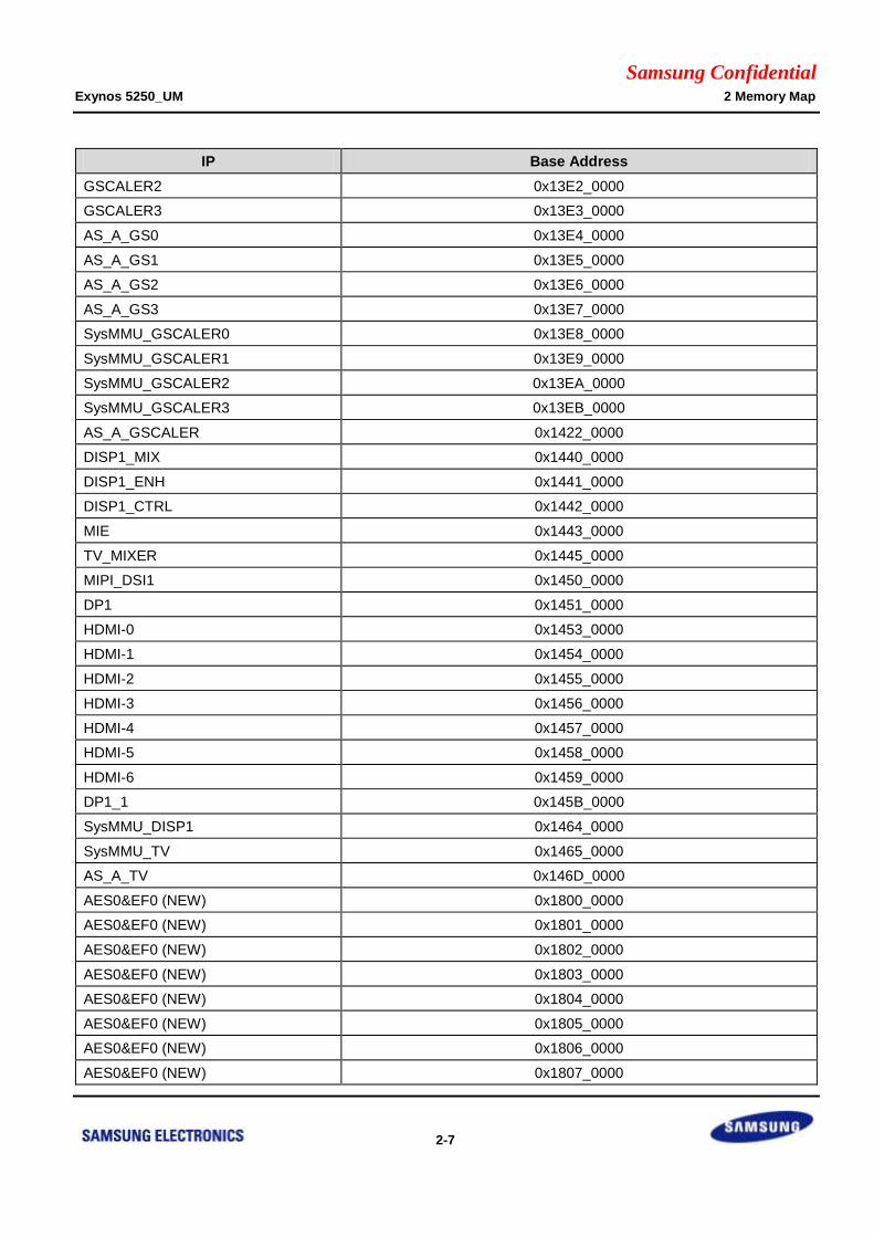
Samsung Confidential Exynos 5250_UM 2 Memory Map
2-7
IP Base Address
GSCALER2 0x13E2_0000
GSCALER3 0x13E3_0000
AS_A_GS0 0x13E4_0000
AS_A_GS1 0x13E5_0000
AS_A_GS2 0x13E6_0000
AS_A_GS3 0x13E7_0000
SysMMU_GSCALER0 0x13E8_0000
SysMMU_GSCALER1 0x13E9_0000
SysMMU_GSCALER2 0x13EA_0000
SysMMU_GSCALER3 0x13EB_0000
AS_A_GSCALER 0x1422_0000
DISP1_MIX 0x1440_0000
DISP1_ENH 0x1441_0000
DISP1_CTRL 0x1442_0000
MIE 0x1443_0000
TV_MIXER 0x1445_0000
MIPI_DSI1 0x1450_0000
DP1 0x1451_0000
HDMI-0 0x1453_0000
HDMI-1 0x1454_0000
HDMI-2 0x1455_0000
HDMI-3 0x1456_0000
HDMI-4 0x1457_0000
HDMI-5 0x1458_0000
HDMI-6 0x1459_0000
DP1_1 0x145B_0000
SysMMU_DISP1 0x1464_0000
SysMMU_TV 0x1465_0000
AS_A_TV 0x146D_0000
AES0&EF0 (NEW) 0x1800_0000
AES0&EF0 (NEW) 0x1801_0000
AES0&EF0 (NEW) 0x1802_0000
AES0&EF0 (NEW) 0x1803_0000
AES0&EF0 (NEW) 0x1804_0000
AES0&EF0 (NEW) 0x1805_0000
AES0&EF0 (NEW) 0x1806_0000
AES0&EF0 (NEW) 0x1807_0000
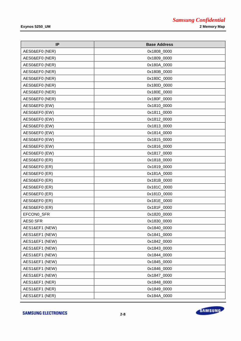
Samsung Confidential Exynos 5250_UM 2 Memory Map
2-8
IP Base Address
AES0&EF0 (NER) 0x1808_0000
AES0&EF0 (NER) 0x1809_0000
AES0&EF0 (NER) 0x180A_0000
AES0&EF0 (NER) 0x180B_0000
AES0&EF0 (NER) 0x180C_0000
AES0&EF0 (NER) 0x180D_0000
AES0&EF0 (NER) 0x180E_0000
AES0&EF0 (NER) 0x180F_0000
AES0&EF0 (EW) 0x1810_0000
AES0&EF0 (EW) 0x1811_0000
AES0&EF0 (EW) 0x1812_0000
AES0&EF0 (EW) 0x1813_0000
AES0&EF0 (EW) 0x1814_0000
AES0&EF0 (EW) 0x1815_0000
AES0&EF0 (EW) 0x1816_0000
AES0&EF0 (EW) 0x1817_0000
AES0&EF0 (ER) 0x1818_0000
AES0&EF0 (ER) 0x1819_0000
AES0&EF0 (ER) 0x181A_0000
AES0&EF0 (ER) 0x181B_0000
AES0&EF0 (ER) 0x181C_0000
AES0&EF0 (ER) 0x181D_0000
AES0&EF0 (ER) 0x181E_0000
AES0&EF0 (ER) 0x181F_0000
EFCON0_SFR 0x1820_0000
AES0 SFR 0x1830_0000
AES1&EF1 (NEW) 0x1840_0000
AES1&EF1 (NEW) 0x1841_0000
AES1&EF1 (NEW) 0x1842_0000
AES1&EF1 (NEW) 0x1843_0000
AES1&EF1 (NEW) 0x1844_0000
AES1&EF1 (NEW) 0x1845_0000
AES1&EF1 (NEW) 0x1846_0000
AES1&EF1 (NEW) 0x1847_0000
AES1&EF1 (NER) 0x1848_0000
AES1&EF1 (NER) 0x1849_0000
AES1&EF1 (NER) 0x184A_0000

Samsung Confidential Exynos 5250_UM 2 Memory Map
2-9
IP Base Address
AES1&EF1 (NER) 0x184B_0000
AES1&EF1 (NER) 0x184C_0000
AES1&EF1 (NER) 0x184D_0000
AES1&EF1 (NER) 0x184E_0000
AES1&EF1 (NER) 0x184F_0000
AES1&EF1 (EW) 0x1850_0000
AES1&EF1 (EW) 0x1851_0000
AES1&EF1 (EW) 0x1852_0000
AES1&EF1 (EW) 0x1853_0000
AES1&EF1 (EW) 0x1854_0000
AES1&EF1 (EW) 0x1855_0000
AES1&EF1 (EW) 0x1856_0000
AES1&EF1 (EW) 0x1857_0000
AES1&EF1 (ER) 0x1858_0000
AES1&EF1 (ER) 0x1859_0000
AES1&EF1 (ER) 0x185A_0000
AES1&EF1 (ER) 0x185B_0000
AES1&EF1 (ER) 0x185C_0000
AES1&EF1 (ER) 0x185D_0000
AES1&EF1 (ER) 0x185E_0000
AES1&EF1 (ER) 0x185F_0000
EFCON1_SFR 0x1860_0000
ns NDMA 0x1868_0000
s NDMA 0x1869_0000
AES1 SFR 0x1870_0000
Samsung Confidential Exynos 5250_UM 3 Chip ID
3-1
3 Chip ID
3.1 Overview
Exynos 5250 contains a Chip ID block for the software (SW). This chip ID sends and receives APB interface
signals to the bus system. You can fine the Chip ID on the first address of the SFR region (0x1000_0000).
The Product ID Register supplies:
Product ID
Revision number
Package information
With the exception of product ID, the electrical fuse ROM (e-from) provides all information bits.

Samsung Confidential Exynos 5250_UM 3 Chip ID
3-2
3.2 Register Description
3.2.1 Register Map Summary
Base Address: 0x1000_0000
Register Offset Description Reset Value
PRO_ID 0x0000 Product information (ID, package, revision) 0x43520XXX
3.2.1.1 PRO_ID
Base Address: 0x1000_0000
Address = Base Address + 0x0000, Reset Value = 0x43520XXX
Name Bit Type Description Reset Value
Product ID [31:12] R
Product ID
0x43520 is the product ID that is allocated to Exynos
5250.
0x43520
Package [11:8] R Package information –
MainRev [7:4] R Main Revision number MainRev. No.
SubRev [3:0] R Sub Revision number SubRev. No.
NOTE: PRO_ID register[7:0] depends on the e-fuse ROM value. The e-fuse ROM values are loaded to the registers during
the power on sequence. It can read the loaded current e-fuse ROM values. An e-fuse ROM consists of main and sub
revision numbers.
Samsung Confidential Exynos 5250_UM 4 Pad Control
4-1
4 Pad Control
4.1 Overview
This chapter describes the General Purpose Input/Output (GPIO).
Exynos 5250 includes:
253 multi-functional input/output port pins
160 memory port pins
There are 39 general port groups and 2 memory port groups. They are:
GPA0, GPA1: 14 in/out ports-2xUART with flow control, UART without flow control, and/or 2xI2C ,
and/or2xHS-I2C
GPA2: 8 in/out ports-2xSPI, and/or I2C
GPB0, GPB1: 10 in/out ports-2xI2S, and/or 2xPCM, and/or AC97, SPDIF, I2C, and/or SPI
GPB2, GPB3: 8 in/out ports-PWM, I2C, and/or I2C ,and/or HS-I2C
GPC0, GPC1: 11 in/out ports-1xMMC (8-bit MMC) I/F
GPC2: 7 in/out ports-1xMMC (4-bit MMC) I/F
GPC3, GPC4: 14 in/out ports-2xMMC (4-bit MMC) and/or 1xMMC (8-bit MMC) I/F
GPD0: 4 pin/out ports-1xUART with flow control I/F
GPD1: 8 pin/out ports-HSI I/F
GPE0, GPE1, GPF0, GPF1, GPG0, GPG1, GPG2, GPH0, GPH1: 48 in/out ports-CAM I/F, and/or Trace I/F
GPV0, GPV1, GPV2, GPV3, GPV4: 34 in/out ports-C2C I/F
GPX0, 1, 2, 3: 32 in/out port-external wake-up interrupts (up-to 32-bit), and/or AUD I/F, and/or MFC I/F (GPX
groups are in alive region)
NOTE: These are in ALIVE region.
Samsung Confidential Exynos 5250_UM 4 Pad Control
4-2
GPY0, GPY1, GPY2: 16 in/out ports-control signals of EBI (SROM)
GPY3, GPY4, GPY5, GPY6: 32 in/out memory ports-EBI
GPZ: 7 in/out ports-low power I2S and/or PCM
NOTE: They can be used for the GPIO, when the power-gating of the MAU is not applied.
MP1_0-MP1_10: 80 DRAM1 ports
NOTE: GPIO registers do not control these ports.
MP2_0-MP2_10: 80 DRAM2 ports
NOTE: GPIO registers do not control these ports.
ETC0, ETC5, ETC6, ETC7, ETC8: 22 in/out ETC ports-JTAG, C2C_CLK (Rx), RESET, CLOCK, USBOTG
and USB3, C2C_CLK (Tx)
Warning: Do not leave a port in input Pull-up/down disable state when neither the port is used nor is connected
to an input pin without Pull-up/down. It may cause unexpected state and leakage current. When a port
is used as output function, ensure to disable Pull-up/down.
Samsung Confidential Exynos 5250_UM 4 Pad Control
4-3
4.2 Features
Features of GPIO are:
Controls 205 External Interrupts
Controls 32 External wake-up Interrupts
Supports 253 multi-functional input/output ports
Controls pin states in sleep mode except GPX0, GPX1, GPX2, and GPX3 (GPX* pins are alive-pads)
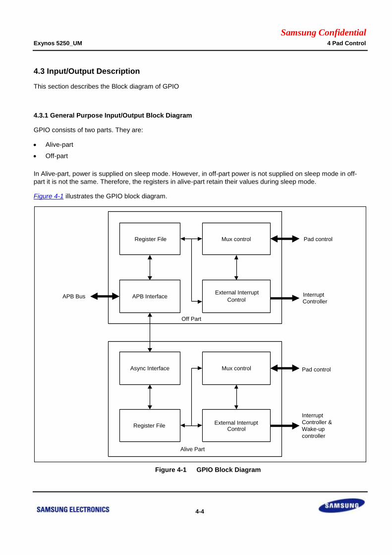
Samsung Confidential Exynos 5250_UM 4 Pad Control
4-4
4.3 Input/Output Description
This section describes the Block diagram of GPIO
4.3.1 General Purpose Input/Output Block Diagram
GPIO consists of two parts. They are:
Alive-part
Off-part
In Alive-part, power is supplied on sleep mode. However, in off-part power is not supplied on sleep mode in off-
part it is not the same. Therefore, the registers in alive-part retain their values during sleep mode.
Figure 4-1 illustrates the GPIO block diagram.
Figure 4-1 GPIO Block Diagram
Alive Part
Pad control
Interrupt
Controller
Pad control
APB Bus
Interrupt
Controller &
Wake-up
controller
Register File Mux control
APB InterfaceExternal Interrupt
Control
Async Interface
Register File
Mux control
External InterruptControl
Off Part
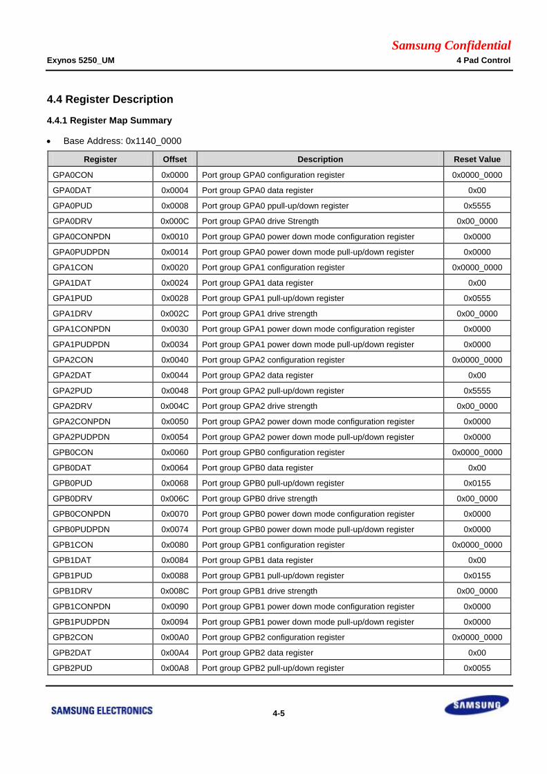
Samsung Confidential Exynos 5250_UM 4 Pad Control
4-5
4.4 Register Description
4.4.1 Register Map Summary
Base Address: 0x1140_0000
Register Offset Description Reset Value
GPA0CON 0x0000 Port group GPA0 configuration register 0x0000_0000
GPA0DAT 0x0004 Port group GPA0 data register 0x00
GPA0PUD 0x0008 Port group GPA0 ppull-up/down register 0x5555
GPA0DRV 0x000C Port group GPA0 drive Strength 0x00_0000
GPA0CONPDN 0x0010 Port group GPA0 power down mode configuration register 0x0000
GPA0PUDPDN 0x0014 Port group GPA0 power down mode pull-up/down register 0x0000
GPA1CON 0x0020 Port group GPA1 configuration register 0x0000_0000
GPA1DAT 0x0024 Port group GPA1 data register 0x00
GPA1PUD 0x0028 Port group GPA1 pull-up/down register 0x0555
GPA1DRV 0x002C Port group GPA1 drive strength 0x00_0000
GPA1CONPDN 0x0030 Port group GPA1 power down mode configuration register 0x0000
GPA1PUDPDN 0x0034 Port group GPA1 power down mode pull-up/down register 0x0000
GPA2CON 0x0040 Port group GPA2 configuration register 0x0000_0000
GPA2DAT 0x0044 Port group GPA2 data register 0x00
GPA2PUD 0x0048 Port group GPA2 pull-up/down register 0x5555
GPA2DRV 0x004C Port group GPA2 drive strength 0x00_0000
GPA2CONPDN 0x0050 Port group GPA2 power down mode configuration register 0x0000
GPA2PUDPDN 0x0054 Port group GPA2 power down mode pull-up/down register 0x0000
GPB0CON 0x0060 Port group GPB0 configuration register 0x0000_0000
GPB0DAT 0x0064 Port group GPB0 data register 0x00
GPB0PUD 0x0068 Port group GPB0 pull-up/down register 0x0155
GPB0DRV 0x006C Port group GPB0 drive strength 0x00_0000
GPB0CONPDN 0x0070 Port group GPB0 power down mode configuration register 0x0000
GPB0PUDPDN 0x0074 Port group GPB0 power down mode pull-up/down register 0x0000
GPB1CON 0x0080 Port group GPB1 configuration register 0x0000_0000
GPB1DAT 0x0084 Port group GPB1 data register 0x00
GPB1PUD 0x0088 Port group GPB1 pull-up/down register 0x0155
GPB1DRV 0x008C Port group GPB1 drive strength 0x00_0000
GPB1CONPDN 0x0090 Port group GPB1 power down mode configuration register 0x0000
GPB1PUDPDN 0x0094 Port group GPB1 power down mode pull-up/down register 0x0000
GPB2CON 0x00A0 Port group GPB2 configuration register 0x0000_0000
GPB2DAT 0x00A4 Port group GPB2 data register 0x00
GPB2PUD 0x00A8 Port group GPB2 pull-up/down register 0x0055
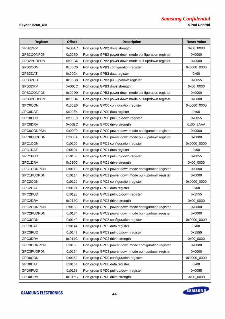
Samsung Confidential Exynos 5250_UM 4 Pad Control
4-6
Register Offset Description Reset Value
GPB2DRV 0x00AC Port group GPB2 drive strength 0x00_0000
GPB2CONPDN 0x00B0 Port group GPB2 power down mode configuration register 0x0000
GPB2PUDPDN 0x00B4 Port group GPB2 power down mode pull-up/down register 0x0000
GPB3CON 0x00C0 Port group GPB3 configuration register 0x0000_0000
GPB3DAT 0x00C4 Port group GPB3 data register 0x00
GPB3PUD 0x00C8 Port group GPB3 pull-up/down register 0x0055
GPB3DRV 0x00CC Port group GPB3 drive strength 0x00_0000
GPB3CONPDN 0x00D0 Port group GPB3 power down mode configuration register 0x0000
GPB3PUDPDN 0x00D4 Port group GPB3 power down mode pull-up/down register 0x0000
GPC0CON 0x00E0 Port group GPC0 configuration register 0x0000_0000
GPC0DAT 0x00E4 Port group GPC0 data register 0x00
GPC0PUD 0x00E8 Port group GPC0 pull-up/down register 0x0055
GPC0DRV 0x00EC Port group GPC0 drive strength 0x00_2AAA
GPC0CONPDN 0x00F0 Port group GPC0 power down mode configuration register 0x0000
GPC0PUDPDN 0x00F4 Port group GPC0 power down mode pull-up/down register 0x0000
GPC1CON 0x0100 Port group GPC1 configuration register 0x0000_0000
GPC1DAT 0x0104 Port group GPC1 data register 0x00
GPC1PUD 0x0108 Port group GPC1 pull-up/down register 0x0055
GPC1DRV 0x010C Port group GPC1 drive strength 0x00_0000
GPC1CONPDN 0x0110 Port group GPC1 power down mode configuration register 0x0000
GPC1PUDPDN 0x0114 Port group GPC1 power down mode pull-up/down register 0x0000
GPC2CON 0x0120 Port group GPC2 configuration register 0x0000_0000
GPC2DAT 0x0124 Port group GPC2 data register 0x00
GPC2PUD 0x0128 Port group GPC2 pull-up/down register 0x1555
GPC2DRV 0x012C Port group GPC2 drive strength 0x00_0000
GPC2CONPDN 0x0130 Port group GPC2 power down mode configuration register 0x0000
GPC2PUDPDN 0x0134 Port group GPC2 power down mode pull-up/down register 0x0000
GPC3CON 0x0140 Port group GPC3 configuration register 0x0000_0000
GPC3DAT 0x0144 Port group GPC3 data register 0x00
GPC3PUD 0x0148 Port group GPC3 pull-up/down register 0x1555
GPC3DRV 0x014C Port group GPC3 drive strength 0x00_0000
GPC3CONPDN 0x0150 Port group GPC3 power down mode configuration register 0x0000
GPC3PUDPDN 0x0154 Port group GPC3 power down mode pull-up/down register 0x0000
GPD0CON 0x0160 Port group GPD0 configuration register 0x0000_0000
GPD0DAT 0x0164 Port group GPD0 data register 0x00
GPD0PUD 0x0168 Port group GPD0 pull-up/down register 0x0055
GPD0DRV 0x016C Port group GPD0 drive strength 0x00_0000

Samsung Confidential Exynos 5250_UM 4 Pad Control
4-7
Register Offset Description Reset Value
GPD0CONPDN 0x0170 Port group GPD0 power down mode configuration register 0x0000
GPD0PUDPDN 0x0174 Port group GPD0 power down mode pull-up/down register 0x0000
GPD1CON 0x0180 Port group GPD1 configuration register 0x0000_0000
GPD1DAT 0x0184 Port group GPD1 data register 0x00
GPD1PUD 0x0188 Port group GPD1 pull-up/down register 0x5555
GPD1DRV 0x018C Port group GPD1 drive strength 0x00_0000
GPD1CONPDN 0x0190 Port group GPD1 power down mode configuration register 0x0000
GPD1PUDPDN 0x0194 Port group GPD1 power down mode pull-up/down register 0x0000
GPY0CON 0x01A0 Port group GPY0 configuration register 0x0000_0000
GPY0DAT 0x01A4 Port group GPY0 data register 0x00
GPY0PUD 0x01A8 Port group GPY0 pull-up/down register 0x0FFF
GPY0DRV 0x01AC Port group GPY0 drive strength 0x00_0AAA
GPY0CONPDN 0x01B0 Port group GPY0 power down mode configuration register 0x0000
GPY0PUDPDN 0x01B4 Port group GPY0 power down mode pull-up/down register 0x0000
GPY1CON 0x01C0 Port group GPY1 configuration register 0x0000_0000
GPY1DAT 0x01C4 Port group GPY1 data register 0x00
GPY1PUD 0x01C8 Port group GPY1 pull-up/down register 0x00FF
GPY1DRV 0x01CC Port group GPY1 drive strength 0x00_00AA
GPY1CONPDN 0x01D0 Port group GPY1 power down mode configuration register 0x0000
GPY1PUDPDN 0x01D4 Port group GPY1 power down mode pull-up/down register 0x0000
GPY2CON 0x01E0 Port group GPY2 configuration register 0x0000_0000
GPY2DAT 0x01E4 Port group GPY2 data register 0x00
GPY2PUD 0x01E8 Port group GPY2 pull-up/down register 0x0FFF
GPY2DRV 0x01EC Port group GPY2 drive strength 0x00_0AAA
GPY2CONPDN 0x01F0 Port group GPY2 power down mode configuration register 0x0000
GPY2PUDPDN 0x01F4 Port group GPY2 power down mode pull-up/down register 0x0000
GPY3CON 0x0200 Port group GPY3 configuration register 0x0000_0000
GPY3DAT 0x0204 Port group GPY3 data register 0x00
GPY3PUD 0x0208 Port group GPY3 pull-up/down register 0x5555
GPY3DRV 0x020C Port group GPY3 drive strength 0x00_AAAA
GPY3CONPDN 0x0210 Port group GPY3 power down mode configuration register 0x0000
GPY3PUDPDN 0x0214 Port group GPY3 power down mode pull-up/down register 0x0000
GPY4CON 0x0220 Port group GPY4 configuration register 0x0000_0000
GPY4DAT 0x0224 Port group GPY4 data register 0x00
GPY4PUD 0x0228 Port group GPY4 pull-up/down register 0x5555
GPY4DRV 0x022C Port group GPY4 drive strength 0x00_AAAA
GPY4CONPDN 0x0230 Port group GPY4 power down mode configuration register 0x0000
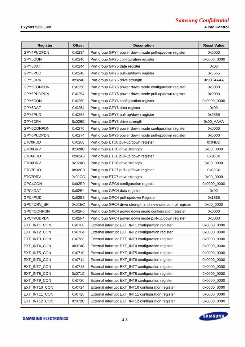
Samsung Confidential Exynos 5250_UM 4 Pad Control
4-8
Register Offset Description Reset Value
GPY4PUDPDN 0x0234 Port group GPY4 power down mode pull-up/down register 0x0000
GPY5CON 0x0240 Port group GPY5 configuration register 0x0000_0000
GPY5DAT 0x0244 Port group GPY5 data register 0x00
GPY5PUD 0x0248 Port group GPY5 pull-up/down register 0x5555
GPY5DRV 0x024C Port group GPY5 drive strength 0x00_AAAA
GPY5CONPDN 0x0250 Port group GPY5 power down mode configuration register 0x0000
GPY5PUDPDN 0x0254 Port group GPY5 power down mode pull-up/down register 0x0000
GPY6CON 0x0260 Port group GPY6 configuration register 0x0000_0000
GPY6DAT 0x0264 Port group GPY6 data register 0x00
GPY6PUD 0x0268 Port group GPY6 pull-up/down register 0x5555
GPY6DRV 0x026C Port group GPY6 drive strength 0x00_AAAA
GPY6CONPDN 0x0270 Port group GPY6 power down mode configuration register 0x0000
GPY6PUDPDN 0x0274 Port group GPY6 power down mode pull-up/down register 0x0000
ETC0PUD 0x0288 Port group ETC0 pull-up/down register 0x04DD
ETC0DRV 0x028C Port group ETC0 drive strength 0x00_0000
ETC6PUD 0x02A8 Port group ETC6 pull-up/down register 0x30C0
ETC6DRV 0x02AC Port group ETC6 drive strength 0x00_0000
ETC7PUD 0x02C8 Port group ETC7 pull-up/down register 0x03C0
ETC7DRV 0x02CC Port group ETC7 drive strength 0x00_0000
GPC4CON 0x02E0 Port group GPC4 configuration register 0x0000_0000
GPC4DAT 0x02E4 Port group GPC4 data register 0x00
GPC4PUD 0x02E8 Port group GPC4 pull-up/down Register 0x1555
GPC4DRV_SR 0x02EC Port group GPC4 drive strength and slew rate control register 0x00_0000
GPC4CONPDN 0x02F0 Port group GPC4 power down mode configuration register 0x0000
GPC4PUDPDN 0x02F4 Port group GPC4 power down mode pull-up/down register 0x0000
EXT_INT1_CON 0x0700 External interrupt EXT_INT1 configuration register 0x0000_0000
EXT_INT2_CON 0x0704 External interrupt EXT_INT2 configuration register 0x0000_0000
EXT_INT3_CON 0x0708 External interrupt EXT_INT3 configuration register 0x0000_0000
EXT_INT4_CON 0x070C External interrupt EXT_INT4 configuration register 0x0000_0000
EXT_INT5_CON 0x0710 External interrupt EXT_INT5 configuration register 0x0000_0000
EXT_INT6_CON 0x0714 External interrupt EXT_INT6 configuration register 0x0000_0000
EXT_INT7_CON 0x0718 External interrupt EXT_INT7 configuration register 0x0000_0000
EXT_INT8_CON 0x071C External interrupt EXT_INT8 configuration register 0x0000_0000
EXT_INT9_CON 0x0720 External interrupt EXT_INT9 configuration register 0x0000_0000
EXT_INT10_CON 0x0724 External interrupt EXT_INT10 configuration register 0x0000_0000
EXT_INT11_CON 0x0728 External interrupt EXT_INT11 configuration register 0x0000_0000
EXT_INT12_CON 0x072C External interrupt EXT_INT12 configuration register 0x0000_0000
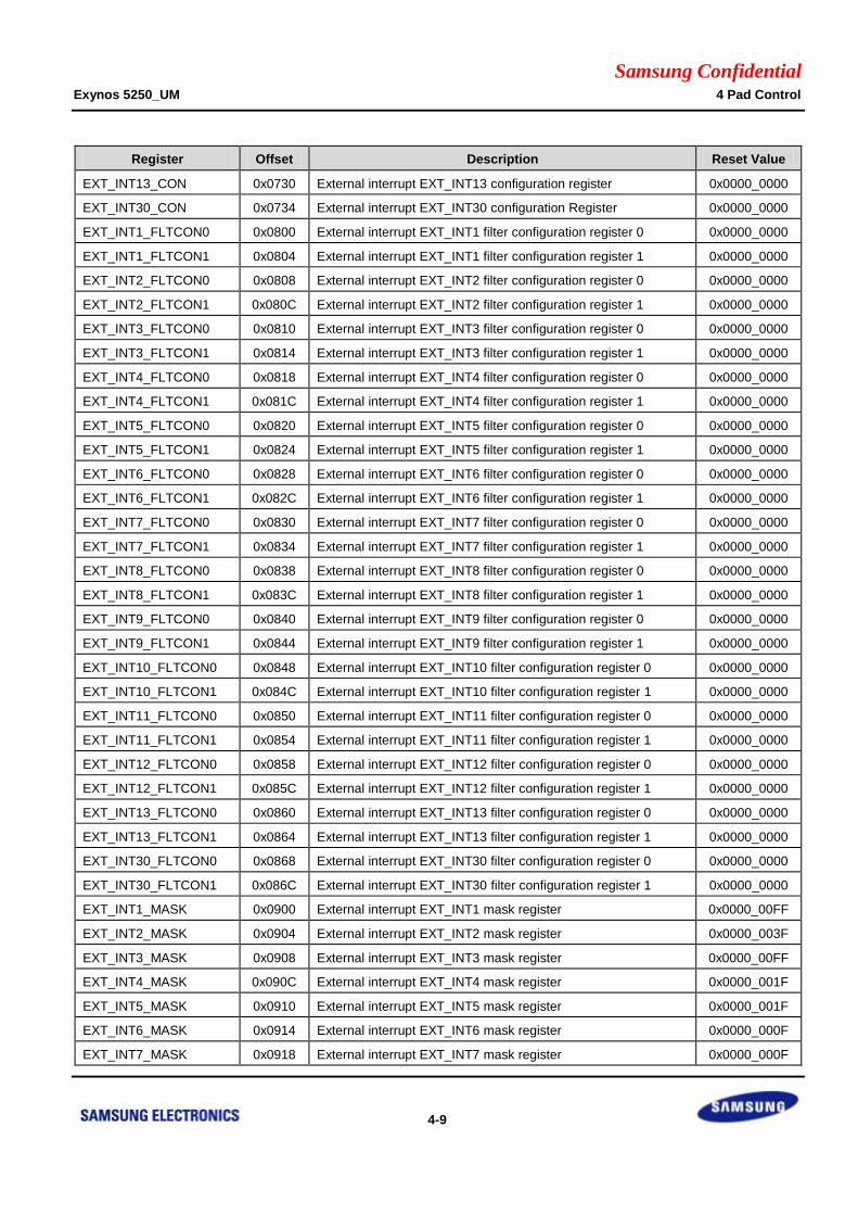
Samsung Confidential Exynos 5250_UM 4 Pad Control
4-9
Register Offset Description Reset Value
EXT_INT13_CON 0x0730 External interrupt EXT_INT13 configuration register 0x0000_0000
EXT_INT30_CON 0x0734 External interrupt EXT_INT30 configuration Register 0x0000_0000
EXT_INT1_FLTCON0 0x0800 External interrupt EXT_INT1 filter configuration register 0 0x0000_0000
EXT_INT1_FLTCON1 0x0804 External interrupt EXT_INT1 filter configuration register 1 0x0000_0000
EXT_INT2_FLTCON0 0x0808 External interrupt EXT_INT2 filter configuration register 0 0x0000_0000
EXT_INT2_FLTCON1 0x080C External interrupt EXT_INT2 filter configuration register 1 0x0000_0000
EXT_INT3_FLTCON0 0x0810 External interrupt EXT_INT3 filter configuration register 0 0x0000_0000
EXT_INT3_FLTCON1 0x0814 External interrupt EXT_INT3 filter configuration register 1 0x0000_0000
EXT_INT4_FLTCON0 0x0818 External interrupt EXT_INT4 filter configuration register 0 0x0000_0000
EXT_INT4_FLTCON1 0x081C External interrupt EXT_INT4 filter configuration register 1 0x0000_0000
EXT_INT5_FLTCON0 0x0820 External interrupt EXT_INT5 filter configuration register 0 0x0000_0000
EXT_INT5_FLTCON1 0x0824 External interrupt EXT_INT5 filter configuration register 1 0x0000_0000
EXT_INT6_FLTCON0 0x0828 External interrupt EXT_INT6 filter configuration register 0 0x0000_0000
EXT_INT6_FLTCON1 0x082C External interrupt EXT_INT6 filter configuration register 1 0x0000_0000
EXT_INT7_FLTCON0 0x0830 External interrupt EXT_INT7 filter configuration register 0 0x0000_0000
EXT_INT7_FLTCON1 0x0834 External interrupt EXT_INT7 filter configuration register 1 0x0000_0000
EXT_INT8_FLTCON0 0x0838 External interrupt EXT_INT8 filter configuration register 0 0x0000_0000
EXT_INT8_FLTCON1 0x083C External interrupt EXT_INT8 filter configuration register 1 0x0000_0000
EXT_INT9_FLTCON0 0x0840 External interrupt EXT_INT9 filter configuration register 0 0x0000_0000
EXT_INT9_FLTCON1 0x0844 External interrupt EXT_INT9 filter configuration register 1 0x0000_0000
EXT_INT10_FLTCON0 0x0848 External interrupt EXT_INT10 filter configuration register 0 0x0000_0000
EXT_INT10_FLTCON1 0x084C External interrupt EXT_INT10 filter configuration register 1 0x0000_0000
EXT_INT11_FLTCON0 0x0850 External interrupt EXT_INT11 filter configuration register 0 0x0000_0000
EXT_INT11_FLTCON1 0x0854 External interrupt EXT_INT11 filter configuration register 1 0x0000_0000
EXT_INT12_FLTCON0 0x0858 External interrupt EXT_INT12 filter configuration register 0 0x0000_0000
EXT_INT12_FLTCON1 0x085C External interrupt EXT_INT12 filter configuration register 1 0x0000_0000
EXT_INT13_FLTCON0 0x0860 External interrupt EXT_INT13 filter configuration register 0 0x0000_0000
EXT_INT13_FLTCON1 0x0864 External interrupt EXT_INT13 filter configuration register 1 0x0000_0000
EXT_INT30_FLTCON0 0x0868 External interrupt EXT_INT30 filter configuration register 0 0x0000_0000
EXT_INT30_FLTCON1 0x086C External interrupt EXT_INT30 filter configuration register 1 0x0000_0000
EXT_INT1_MASK 0x0900 External interrupt EXT_INT1 mask register 0x0000_00FF
EXT_INT2_MASK 0x0904 External interrupt EXT_INT2 mask register 0x0000_003F
EXT_INT3_MASK 0x0908 External interrupt EXT_INT3 mask register 0x0000_00FF
EXT_INT4_MASK 0x090C External interrupt EXT_INT4 mask register 0x0000_001F
EXT_INT5_MASK 0x0910 External interrupt EXT_INT5 mask register 0x0000_001F
EXT_INT6_MASK 0x0914 External interrupt EXT_INT6 mask register 0x0000_000F
EXT_INT7_MASK 0x0918 External interrupt EXT_INT7 mask register 0x0000_000F
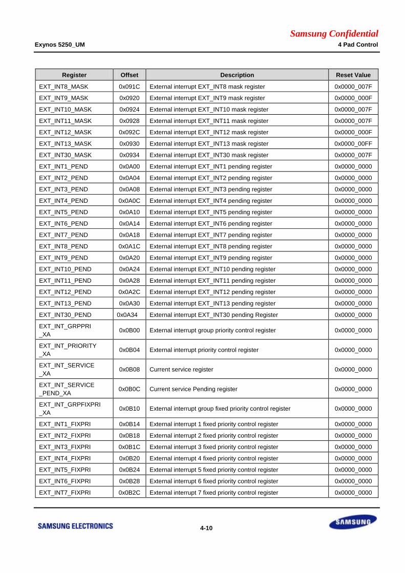
Samsung Confidential Exynos 5250_UM 4 Pad Control
4-10
Register Offset Description Reset Value
EXT_INT8_MASK 0x091C External interrupt EXT_INT8 mask register 0x0000_007F
EXT_INT9_MASK 0x0920 External interrupt EXT_INT9 mask register 0x0000_000F
EXT_INT10_MASK 0x0924 External interrupt EXT_INT10 mask register 0x0000_007F
EXT_INT11_MASK 0x0928 External interrupt EXT_INT11 mask register 0x0000_007F
EXT_INT12_MASK 0x092C External interrupt EXT_INT12 mask register 0x0000_000F
EXT_INT13_MASK 0x0930 External interrupt EXT_INT13 mask register 0x0000_00FF
EXT_INT30_MASK 0x0934 External interrupt EXT_INT30 mask register 0x0000_007F
EXT_INT1_PEND 0x0A00 External interrupt EXT_INT1 pending register 0x0000_0000
EXT_INT2_PEND 0x0A04 External interrupt EXT_INT2 pending register 0x0000_0000
EXT_INT3_PEND 0x0A08 External interrupt EXT_INT3 pending register 0x0000_0000
EXT_INT4_PEND 0x0A0C External interrupt EXT_INT4 pending register 0x0000_0000
EXT_INT5_PEND 0x0A10 External interrupt EXT_INT5 pending register 0x0000_0000
EXT_INT6_PEND 0x0A14 External interrupt EXT_INT6 pending register 0x0000_0000
EXT_INT7_PEND 0x0A18 External interrupt EXT_INT7 pending register 0x0000_0000
EXT_INT8_PEND 0x0A1C External interrupt EXT_INT8 pending register 0x0000_0000
EXT_INT9_PEND 0x0A20 External interrupt EXT_INT9 pending register 0x0000_0000
EXT_INT10_PEND 0x0A24 External interrupt EXT_INT10 pending register 0x0000_0000
EXT_INT11_PEND 0x0A28 External interrupt EXT_INT11 pending register 0x0000_0000
EXT_INT12_PEND 0x0A2C External interrupt EXT_INT12 pending register 0x0000_0000
EXT_INT13_PEND 0x0A30 External interrupt EXT_INT13 pending register 0x0000_0000
EXT_INT30_PEND 0x0A34 External interrupt EXT_INT30 pending Register 0x0000_0000
EXT_INT_GRPPRI
_XA 0x0B00 External interrupt group priority control register 0x0000_0000
EXT_INT_PRIORITY
_XA 0x0B04 External interrupt priority control register 0x0000_0000
EXT_INT_SERVICE
_XA 0x0B08 Current service register 0x0000_0000
EXT_INT_SERVICE
_PEND_XA 0x0B0C Current service Pending register 0x0000_0000
EXT_INT_GRPFIXPRI
_XA 0x0B10 External interrupt group fixed priority control register 0x0000_0000
EXT_INT1_FIXPRI 0x0B14 External interrupt 1 fixed priority control register 0x0000_0000
EXT_INT2_FIXPRI 0x0B18 External interrupt 2 fixed priority control register 0x0000_0000
EXT_INT3_FIXPRI 0x0B1C External interrupt 3 fixed priority control register 0x0000_0000
EXT_INT4_FIXPRI 0x0B20 External interrupt 4 fixed priority control register 0x0000_0000
EXT_INT5_FIXPRI 0x0B24 External interrupt 5 fixed priority control register 0x0000_0000
EXT_INT6_FIXPRI 0x0B28 External interrupt 6 fixed priority control register 0x0000_0000
EXT_INT7_FIXPRI 0x0B2C External interrupt 7 fixed priority control register 0x0000_0000
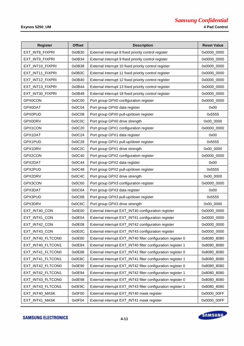
Samsung Confidential Exynos 5250_UM 4 Pad Control
4-11
Register Offset Description Reset Value
EXT_INT8_FIXPRI 0x0B30 External interrupt 8 fixed priority control register 0x0000_0000
EXT_INT9_FIXPRI 0x0B34 External interrupt 9 fixed priority control register 0x0000_0000
EXT_INT10_FIXPRI 0x0B38 External interrupt 10 fixed priority control register 0x0000_0000
EXT_INT11_FIXPRI 0x0B3C External interrupt 11 fixed priority control register 0x0000_0000
EXT_INT12_FIXPRI 0x0B40 External interrupt 12 fixed priority control register 0x0000_0000
EXT_INT13_FIXPRI 0x0B44 External interrupt 13 fixed priority control register 0x0000_0000
EXT_INT30_FIXPRI 0x0B48 External interrupt 18 fixed priority control register 0x0000_0000
GPX0CON 0x0C00 Port group GPX0 configuration register 0x0000_0000
GPX0DAT 0x0C04 Port group GPX0 data register 0x00
GPX0PUD 0x0C08 Port group GPX0 pull-up/down register 0x5555
GPX0DRV 0x0C0C Port group GPX0 drive strength 0x00_0000
GPX1CON 0x0C20 Port group GPX1 configuration register 0x0000_0000
GPX1DAT 0x0C24 Port group GPX1 data register 0x00
GPX1PUD 0x0C28 Port group GPX1 pull-up/down register 0x5555
GPX1DRV 0x0C2C Port group GPX1 drive strength 0x00_0000
GPX2CON 0x0C40 Port group GPX2 configuration register 0x0000_0000
GPX2DAT 0x0C44 Port group GPX2 data register 0x00
GPX2PUD 0x0C48 Port group GPX2 pull-up/down register 0x5555
GPX2DRV 0x0C4C Port group GPX2 drive strength 0x00_0000
GPX3CON 0x0C60 Port group GPX3 configuration register 0x0000_0000
GPX3DAT 0x0C64 Port group GPX3 data register 0x00
GPX3PUD 0x0C68 Port group GPX3 pull-up/down register 0x5555
GPX3DRV 0x0C6C Port group GPX3 drive strength 0x00_0000
EXT_INT40_CON 0x0E00 External interrupt EXT_INT40 configuration register 0x0000_0000
EXT_INT41_CON 0x0E04 External interrupt EXT_INT41 configuration register 0x0000_0000
EXT_INT42_CON 0x0E08 External interrupt EXT_INT42 configuration register 0x0000_0000
EXT_INT43_CON 0x0E0C External interrupt EXT_INT43 configuration register 0x0000_0000
EXT_INT40_FLTCON0 0x0E80 External interrupt EXT_INT40 filter configuration register 0 0x8080_8080
EXT_INT40_FLTCON1 0x0E84 External interrupt EXT_INT40 filter configuration register 1 0x8080_8080
EXT_INT41_FLTCON0 0x0E88 External interrupt EXT_INT41 filter configuration register 0 0x8080_8080
EXT_INT41_FLTCON1 0x0E8C External interrupt EXT_INT41 filter configuration register 1 0x8080_8080
EXT_INT42_FLTCON0 0x0E90 External interrupt EXT_INT42 filter configuration register 0 0x8080_8080
EXT_INT42_FLTCON1 0x0E94 External interrupt EXT_INT42 filter configuration register 1 0x8080_8080
EXT_INT43_FLTCON0 0x0E98 External interrupt EXT_INT43 filter configuration register 0 0x8080_8080
EXT_INT43_FLTCON1 0x0E9C External interrupt EXT_INT43 filter configuration register 1 0x8080_8080
EXT_INT40_MASK 0x0F00 External interrupt EXT_INT40 mask register 0x0000_00FF
EXT_INT41_MASK 0x0F04 External interrupt EXT_INT41 mask register 0x0000_00FF
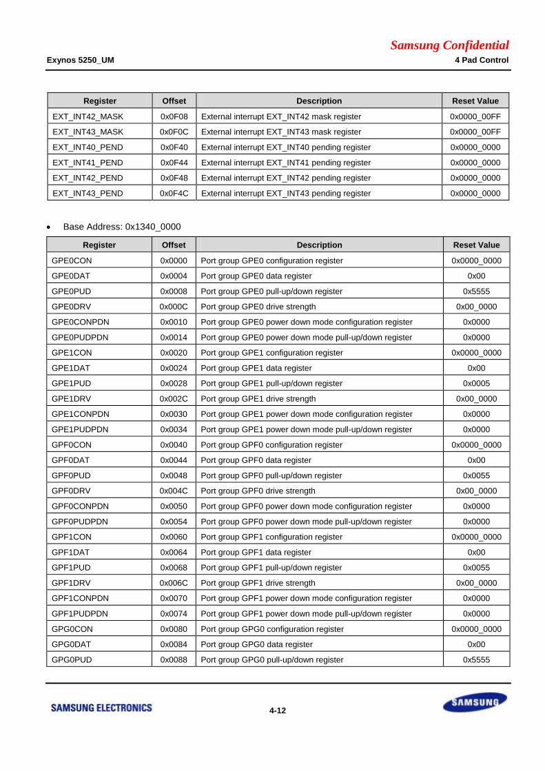
Samsung Confidential Exynos 5250_UM 4 Pad Control
4-12
Register Offset Description Reset Value
EXT_INT42_MASK 0x0F08 External interrupt EXT_INT42 mask register 0x0000_00FF
EXT_INT43_MASK 0x0F0C External interrupt EXT_INT43 mask register 0x0000_00FF
EXT_INT40_PEND 0x0F40 External interrupt EXT_INT40 pending register 0x0000_0000
EXT_INT41_PEND 0x0F44 External interrupt EXT_INT41 pending register 0x0000_0000
EXT_INT42_PEND 0x0F48 External interrupt EXT_INT42 pending register 0x0000_0000
EXT_INT43_PEND 0x0F4C External interrupt EXT_INT43 pending register 0x0000_0000
Base Address: 0x1340_0000
Register Offset Description Reset Value
GPE0CON 0x0000 Port group GPE0 configuration register 0x0000_0000
GPE0DAT 0x0004 Port group GPE0 data register 0x00
GPE0PUD 0x0008 Port group GPE0 pull-up/down register 0x5555
GPE0DRV 0x000C Port group GPE0 drive strength 0x00_0000
GPE0CONPDN 0x0010 Port group GPE0 power down mode configuration register 0x0000
GPE0PUDPDN 0x0014 Port group GPE0 power down mode pull-up/down register 0x0000
GPE1CON 0x0020 Port group GPE1 configuration register 0x0000_0000
GPE1DAT 0x0024 Port group GPE1 data register 0x00
GPE1PUD 0x0028 Port group GPE1 pull-up/down register 0x0005
GPE1DRV 0x002C Port group GPE1 drive strength 0x00_0000
GPE1CONPDN 0x0030 Port group GPE1 power down mode configuration register 0x0000
GPE1PUDPDN 0x0034 Port group GPE1 power down mode pull-up/down register 0x0000
GPF0CON 0x0040 Port group GPF0 configuration register 0x0000_0000
GPF0DAT 0x0044 Port group GPF0 data register 0x00
GPF0PUD 0x0048 Port group GPF0 pull-up/down register 0x0055
GPF0DRV 0x004C Port group GPF0 drive strength 0x00_0000
GPF0CONPDN 0x0050 Port group GPF0 power down mode configuration register 0x0000
GPF0PUDPDN 0x0054 Port group GPF0 power down mode pull-up/down register 0x0000
GPF1CON 0x0060 Port group GPF1 configuration register 0x0000_0000
GPF1DAT 0x0064 Port group GPF1 data register 0x00
GPF1PUD 0x0068 Port group GPF1 pull-up/down register 0x0055
GPF1DRV 0x006C Port group GPF1 drive strength 0x00_0000
GPF1CONPDN 0x0070 Port group GPF1 power down mode configuration register 0x0000
GPF1PUDPDN 0x0074 Port group GPF1 power down mode pull-up/down register 0x0000
GPG0CON 0x0080 Port group GPG0 configuration register 0x0000_0000
GPG0DAT 0x0084 Port group GPG0 data register 0x00
GPG0PUD 0x0088 Port group GPG0 pull-up/down register 0x5555
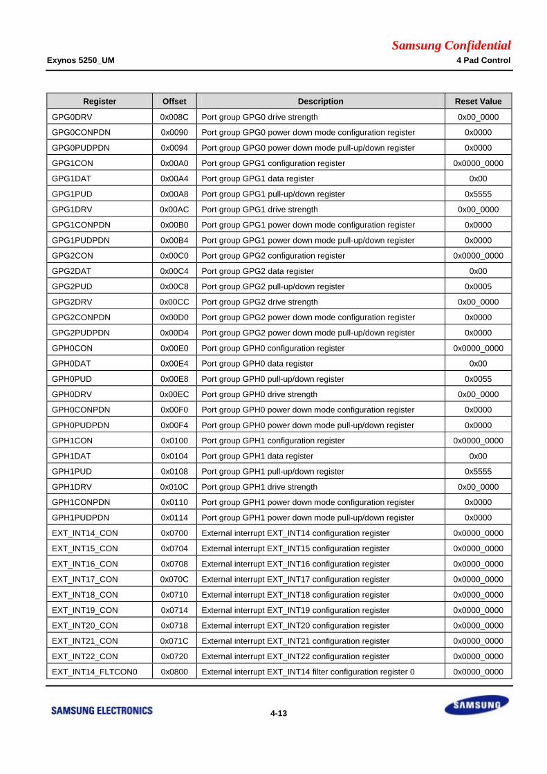
Samsung Confidential Exynos 5250_UM 4 Pad Control
4-13
Register Offset Description Reset Value
GPG0DRV 0x008C Port group GPG0 drive strength 0x00_0000
GPG0CONPDN 0x0090 Port group GPG0 power down mode configuration register 0x0000
GPG0PUDPDN 0x0094 Port group GPG0 power down mode pull-up/down register 0x0000
GPG1CON 0x00A0 Port group GPG1 configuration register 0x0000_0000
GPG1DAT 0x00A4 Port group GPG1 data register 0x00
GPG1PUD 0x00A8 Port group GPG1 pull-up/down register 0x5555
GPG1DRV 0x00AC Port group GPG1 drive strength 0x00_0000
GPG1CONPDN 0x00B0 Port group GPG1 power down mode configuration register 0x0000
GPG1PUDPDN 0x00B4 Port group GPG1 power down mode pull-up/down register 0x0000
GPG2CON 0x00C0 Port group GPG2 configuration register 0x0000_0000
GPG2DAT 0x00C4 Port group GPG2 data register 0x00
GPG2PUD 0x00C8 Port group GPG2 pull-up/down register 0x0005
GPG2DRV 0x00CC Port group GPG2 drive strength 0x00_0000
GPG2CONPDN 0x00D0 Port group GPG2 power down mode configuration register 0x0000
GPG2PUDPDN 0x00D4 Port group GPG2 power down mode pull-up/down register 0x0000
GPH0CON 0x00E0 Port group GPH0 configuration register 0x0000_0000
GPH0DAT 0x00E4 Port group GPH0 data register 0x00
GPH0PUD 0x00E8 Port group GPH0 pull-up/down register 0x0055
GPH0DRV 0x00EC Port group GPH0 drive strength 0x00_0000
GPH0CONPDN 0x00F0 Port group GPH0 power down mode configuration register 0x0000
GPH0PUDPDN 0x00F4 Port group GPH0 power down mode pull-up/down register 0x0000
GPH1CON 0x0100 Port group GPH1 configuration register 0x0000_0000
GPH1DAT 0x0104 Port group GPH1 data register 0x00
GPH1PUD 0x0108 Port group GPH1 pull-up/down register 0x5555
GPH1DRV 0x010C Port group GPH1 drive strength 0x00_0000
GPH1CONPDN 0x0110 Port group GPH1 power down mode configuration register 0x0000
GPH1PUDPDN 0x0114 Port group GPH1 power down mode pull-up/down register 0x0000
EXT_INT14_CON 0x0700 External interrupt EXT_INT14 configuration register 0x0000_0000
EXT_INT15_CON 0x0704 External interrupt EXT_INT15 configuration register 0x0000_0000
EXT_INT16_CON 0x0708 External interrupt EXT_INT16 configuration register 0x0000_0000
EXT_INT17_CON 0x070C External interrupt EXT_INT17 configuration register 0x0000_0000
EXT_INT18_CON 0x0710 External interrupt EXT_INT18 configuration register 0x0000_0000
EXT_INT19_CON 0x0714 External interrupt EXT_INT19 configuration register 0x0000_0000
EXT_INT20_CON 0x0718 External interrupt EXT_INT20 configuration register 0x0000_0000
EXT_INT21_CON 0x071C External interrupt EXT_INT21 configuration register 0x0000_0000
EXT_INT22_CON 0x0720 External interrupt EXT_INT22 configuration register 0x0000_0000
EXT_INT14_FLTCON0 0x0800 External interrupt EXT_INT14 filter configuration register 0 0x0000_0000
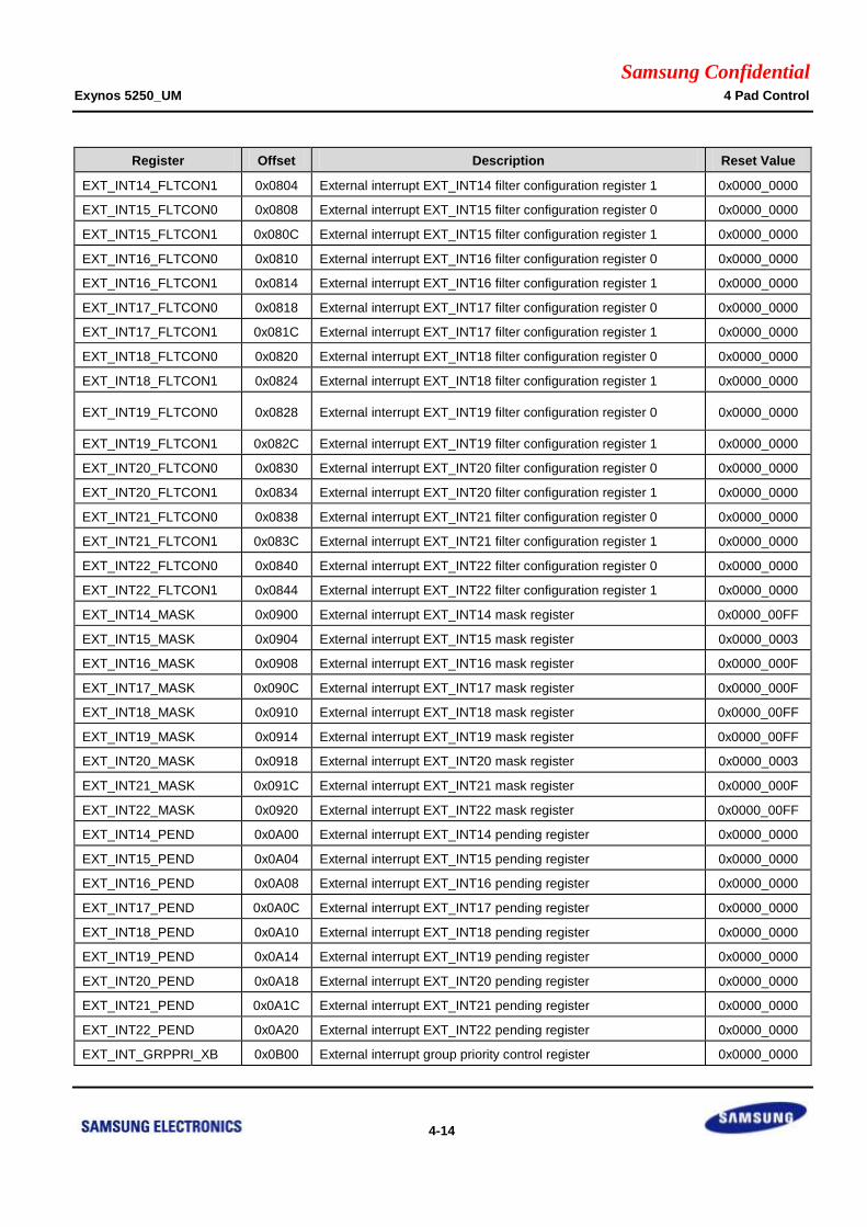
Samsung Confidential Exynos 5250_UM 4 Pad Control
4-14
Register Offset Description Reset Value
EXT_INT14_FLTCON1 0x0804 External interrupt EXT_INT14 filter configuration register 1 0x0000_0000
EXT_INT15_FLTCON0 0x0808 External interrupt EXT_INT15 filter configuration register 0 0x0000_0000
EXT_INT15_FLTCON1 0x080C External interrupt EXT_INT15 filter configuration register 1 0x0000_0000
EXT_INT16_FLTCON0 0x0810 External interrupt EXT_INT16 filter configuration register 0 0x0000_0000
EXT_INT16_FLTCON1 0x0814 External interrupt EXT_INT16 filter configuration register 1 0x0000_0000
EXT_INT17_FLTCON0 0x0818 External interrupt EXT_INT17 filter configuration register 0 0x0000_0000
EXT_INT17_FLTCON1 0x081C External interrupt EXT_INT17 filter configuration register 1 0x0000_0000
EXT_INT18_FLTCON0 0x0820 External interrupt EXT_INT18 filter configuration register 0 0x0000_0000
EXT_INT18_FLTCON1 0x0824 External interrupt EXT_INT18 filter configuration register 1 0x0000_0000
EXT_INT19_FLTCON0 0x0828 External interrupt EXT_INT19 filter configuration register 0 0x0000_0000
EXT_INT19_FLTCON1 0x082C External interrupt EXT_INT19 filter configuration register 1 0x0000_0000
EXT_INT20_FLTCON0 0x0830 External interrupt EXT_INT20 filter configuration register 0 0x0000_0000
EXT_INT20_FLTCON1 0x0834 External interrupt EXT_INT20 filter configuration register 1 0x0000_0000
EXT_INT21_FLTCON0 0x0838 External interrupt EXT_INT21 filter configuration register 0 0x0000_0000
EXT_INT21_FLTCON1 0x083C External interrupt EXT_INT21 filter configuration register 1 0x0000_0000
EXT_INT22_FLTCON0 0x0840 External interrupt EXT_INT22 filter configuration register 0 0x0000_0000
EXT_INT22_FLTCON1 0x0844 External interrupt EXT_INT22 filter configuration register 1 0x0000_0000
EXT_INT14_MASK 0x0900 External interrupt EXT_INT14 mask register 0x0000_00FF
EXT_INT15_MASK 0x0904 External interrupt EXT_INT15 mask register 0x0000_0003
EXT_INT16_MASK 0x0908 External interrupt EXT_INT16 mask register 0x0000_000F
EXT_INT17_MASK 0x090C External interrupt EXT_INT17 mask register 0x0000_000F
EXT_INT18_MASK 0x0910 External interrupt EXT_INT18 mask register 0x0000_00FF
EXT_INT19_MASK 0x0914 External interrupt EXT_INT19 mask register 0x0000_00FF
EXT_INT20_MASK 0x0918 External interrupt EXT_INT20 mask register 0x0000_0003
EXT_INT21_MASK 0x091C External interrupt EXT_INT21 mask register 0x0000_000F
EXT_INT22_MASK 0x0920 External interrupt EXT_INT22 mask register 0x0000_00FF
EXT_INT14_PEND 0x0A00 External interrupt EXT_INT14 pending register 0x0000_0000
EXT_INT15_PEND 0x0A04 External interrupt EXT_INT15 pending register 0x0000_0000
EXT_INT16_PEND 0x0A08 External interrupt EXT_INT16 pending register 0x0000_0000
EXT_INT17_PEND 0x0A0C External interrupt EXT_INT17 pending register 0x0000_0000
EXT_INT18_PEND 0x0A10 External interrupt EXT_INT18 pending register 0x0000_0000
EXT_INT19_PEND 0x0A14 External interrupt EXT_INT19 pending register 0x0000_0000
EXT_INT20_PEND 0x0A18 External interrupt EXT_INT20 pending register 0x0000_0000
EXT_INT21_PEND 0x0A1C External interrupt EXT_INT21 pending register 0x0000_0000
EXT_INT22_PEND 0x0A20 External interrupt EXT_INT22 pending register 0x0000_0000
EXT_INT_GRPPRI_XB 0x0B00 External interrupt group priority control register 0x0000_0000
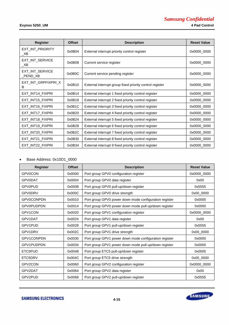
Samsung Confidential Exynos 5250_UM 4 Pad Control
4-15
Register Offset Description Reset Value
EXT_INT_PRIORITY
_XB 0x0B04 External interrupt priority control register 0x0000_0000
EXT_INT_SERVICE
_XB 0x0B08 Current service register 0x0000_0000
EXT_INT_SERVICE
_PEND_XB 0x0B0C Current service pending register 0x0000_0000
EXT_INT_GRPFIXPRI_X
B 0x0B10 External interrupt group fixed priority control register 0x0000_0000
EXT_INT14_FIXPRI 0x0B14 External interrupt 1 fixed priority control register 0x0000_0000
EXT_INT15_FIXPRI 0x0B18 External interrupt 2 fixed priority control register 0x0000_0000
EXT_INT16_FIXPRI 0x0B1C External interrupt 3 fixed priority control register 0x0000_0000
EXT_INT17_FIXPRI 0x0B20 External interrupt 4 fixed priority control register 0x0000_0000
EXT_INT18_FIXPRI 0x0B24 External interrupt 5 fixed priority control register 0x0000_0000
EXT_INT19_FIXPRI 0x0B28 External interrupt 6 fixed priority control register 0x0000_0000
EXT_INT20_FIXPRI 0x0B2C External interrupt 7 fixed priority control register 0x0000_0000
EXT_INT21_FIXPRI 0x0B30 External interrupt 8 fixed priority control register 0x0000_0000
EXT_INT22_FIXPRI 0x0B34 External interrupt 9 fixed priority control register 0x0000_0000
Base Address: 0x10D1_0000
Register Offset Description Reset Value
GPV0CON 0x0000 Port group GPV0 configuration register 0x0000_0000
GPV0DAT 0x0004 Port group GPV0 data register 0x00
GPV0PUD 0x0008 Port group GPV0 pull-up/down register 0x5555
GPV0DRV 0x000C Port group GPV0 drive strength 0x00_0000
GPV0CONPDN 0x0010 Port group GPV0 power down mode configuration register 0x0000
GPV0PUDPDN 0x0014 Port group GPV0 power down mode pull-up/down register 0x0000
GPV1CON 0x0020 Port group GPV1 configuration register 0x0000_0000
GPV1DAT 0x0024 Port group GPV1 data register 0x00
GPV1PUD 0x0028 Port group GPV1 pull-up/down register 0x5555
GPV1DRV 0x002C Port group GPV1 drive strength 0x00_0000
GPV1CONPDN 0x0030 Port group GPV1 power down mode configuration register 0x0000
GPV1PUDPDN 0x0034 Port group GPV1 power down mode pull-up/down register 0x0000
ETC5PUD 0x0048 Port group ETC5 pull-up/down register 0x0005
ETC5DRV 0x004C Port group ETC5 drive strength 0x00_0000
GPV2CON 0x0060 Port group GPV2 configuration register 0x0000_0000
GPV2DAT 0x0064 Port group GPV2 data register 0x00
GPV2PUD 0x0068 Port group GPV2 pull-up/down register 0x5555
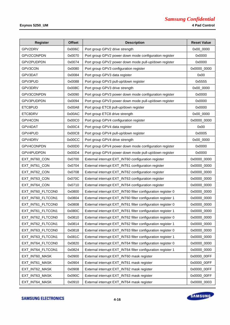
Samsung Confidential Exynos 5250_UM 4 Pad Control
4-16
Register Offset Description Reset Value
GPV2DRV 0x006C Port group GPV2 drive strength 0x00_0000
GPV2CONPDN 0x0070 Port group GPV2 power down mode configuration register 0x0000
GPV2PUDPDN 0x0074 Port group GPV2 power down mode pull-up/down register 0x0000
GPV3CON 0x0080 Port group GPV3 configuration register 0x0000_0000
GPV3DAT 0x0084 Port group GPV3 data register 0x00
GPV3PUD 0x0088 Port group GPV3 pull-up/down register 0x5555
GPV3DRV 0x008C Port group GPV3 drive strength 0x00_0000
GPV3CONPDN 0x0090 Port group GPV3 power down mode configuration register 0x0000
GPV3PUDPDN 0x0094 Port group GPV3 power down mode pull-up/down register 0x0000
ETC8PUD 0x00A8 Port group ETC8 pull-up/down register 0x0000
ETC8DRV 0x00AC Port group ETC8 drive strength 0x00_0000
GPV4CON 0x00C0 Port group GPV4 configuration register 0x0000_0000
GPV4DAT 0x00C4 Port group GPV4 data register 0x00
GPV4PUD 0x00C8 Port group GPV4 pull-up/down register 0x0005
GPV4DRV 0x00CC Port group GPV4 drive strength 0x00_0000
GPV4CONPDN 0x00D0 Port group GPV4 power down mode configuration register 0x0000
GPV4PUDPDN 0x00D4 Port group GPV4 power down mode pull-up/down register 0x0000
EXT_INT60_CON 0x0700 External interrupt EXT_INT60 configuration register 0x0000_0000
EXT_INT61_CON 0x0704 External interrupt EXT_INT61 configuration register 0x0000_0000
EXT_INT62_CON 0x0708 External interrupt EXT_INT62 configuration register 0x0000_0000
EXT_INT63_CON 0x070C External interrupt EXT_INT63 configuration register 0x0000_0000
EXT_INT64_CON 0x0710 External interrupt EXT_INT64 configuration register 0x0000_0000
EXT_INT60_FLTCON0 0x0800 External interrupt EXT_INT60 filter configuration register 0 0x0000_0000
EXT_INT60_FLTCON1 0x0804 External interrupt EXT_INT60 filter configuration register 1 0x0000_0000
EXT_INT61_FLTCON0 0x0808 External interrupt EXT_INT61 filter configuration register 0 0x0000_0000
EXT_INT61_FLTCON1 0x080C External interrupt EXT_INT61 filter configuration register 1 0x0000_0000
EXT_INT62_FLTCON0 0x0810 External interrupt EXT_INT62 filter configuration register 0 0x0000_0000
EXT_INT62_FLTCON1 0x0814 External interrupt EXT_INT62 filter configuration register 1 0x0000_0000
EXT_INT63_FLTCON0 0x0818 External interrupt EXT_INT63 filter configuration register 0 0x0000_0000
EXT_INT63_FLTCON1 0x081C External interrupt EXT_INT63 filter configuration register 1 0x0000_0000
EXT_INT64_FLTCON0 0x0820 External interrupt EXT_INT64 filter configuration register 0 0x0000_0000
EXT_INT64_FLTCON1 0x0824 External interrupt EXT_INT64 filter configuration register 1 0x0000_0000
EXT_INT60_MASK 0x0900 External interrupt EXT_INT60 mask register 0x0000_00FF
EXT_INT61_MASK 0x0904 External interrupt EXT_INT61 mask register 0x0000_00FF
EXT_INT62_MASK 0x0908 External interrupt EXT_INT62 mask register 0x0000_00FF
EXT_INT63_MASK 0x090C External interrupt EXT_INT63 mask register 0x0000_00FF
EXT_INT64_MASK 0x0910 External interrupt EXT_INT64 mask register 0x0000_0003

Samsung Confidential Exynos 5250_UM 4 Pad Control
4-17
Register Offset Description Reset Value
EXT_INT60_PEND 0x0A00 External interrupt EXT_INT60 Pending register 0x0000_0000
EXT_INT61_PEND 0x0A04 External interrupt EXT_INT61 Pending register 0x0000_0000
EXT_INT62_PEND 0x0A08 External interrupt EXT_INT62 Pending register 0x0000_0000
EXT_INT63_PEND 0x0A0C External interrupt EXT_INT63 Pending register 0x0000_0000
EXT_INT64_PEND 0x0A10 External interrupt EXT_INT64 Pending register 0x0000_0000
EXT_INT_GRPPRI
_XC 0x0B00 External interrupt group priority control register 0x0000_0000
EXT_INT_PRIORITY
_XC 0x0B04 External interrupt priority control register 0x0000_0000
EXT_INT_SERVICE
_XC 0x0B08 Current service register 0x0000_0000
EXT_INT_SERVICE
_PEND_XC 0x0B0C Current service pending register 0x0000_0000
EXT_INT_GRPFIXPRI_X
C 0x0B10 External interrupt group fixed priority control register 0x0000_0000
EXT_INT60_FIXPRI 0x0B14 External interrupt 1 fixed priority control register 0x0000_0000
EXT_INT61_FIXPRI 0x0B18 External interrupt 2 fixed priority control register 0x0000_0000
EXT_INT62_FIXPRI 0x0B1C External interrupt 3 fixed priority control register 0x0000_0000
EXT_INT63_FIXPRI 0x0B20 External interrupt 4 fixed priority control register 0x0000_0000
EXT_INT64_FIXPRI 0x0B24 External interrupt 5 fixed priority control register 0x0000_0000
Base Address: 0x0386_0000
Register Offset Description Reset Value
GPZCON 0x0000 Port group GPZ configuration register 0x0000_0000
GPZDAT 0x0004 Port group GPZ data register 0x00
GPZPUD 0x0008 Port group GPZ pull-up/down register 0x1555
GPZDRV 0x000C Port group GPZ drive strength 0x00_0000
GPZCONPDN 0x0010 Port group GPZ power down mode configuration register 0x0000
GPZPUDPDN 0x0014 Port group GPZ power down mode pull-up/down register 0x0000
EXT_INT50_CON 0x0700 External interrupt EXT_INT50 configuration register 0x0000_0000
EXT_INT50_FLTCON0 0x0800 External interrupt EXT_INT50 filter configuration register 0 0x0000_0000
EXT_INT50_FLTCON1 0x0804 External interrupt EXT_INT50 filter configuration register 1 0x0000_0000
EXT_INT50_MASK 0x0900 External interrupt EXT_INT50 mask register 0x0000_007F
EXT_INT50_PEND 0x0A00 External interrupt EXT_INT50 pending register 0x0000_0000
EXT_INT_GRPPRI_XD 0x0B00 External interrupt group priority control register 0x0000_0000
EXT_INT_PRIORITY
_XD 0x0B04 External interrupt priority control register 0x0000_0000
EXT_INT_SERVICE 0x0B08 Current service register 0x0000_0000
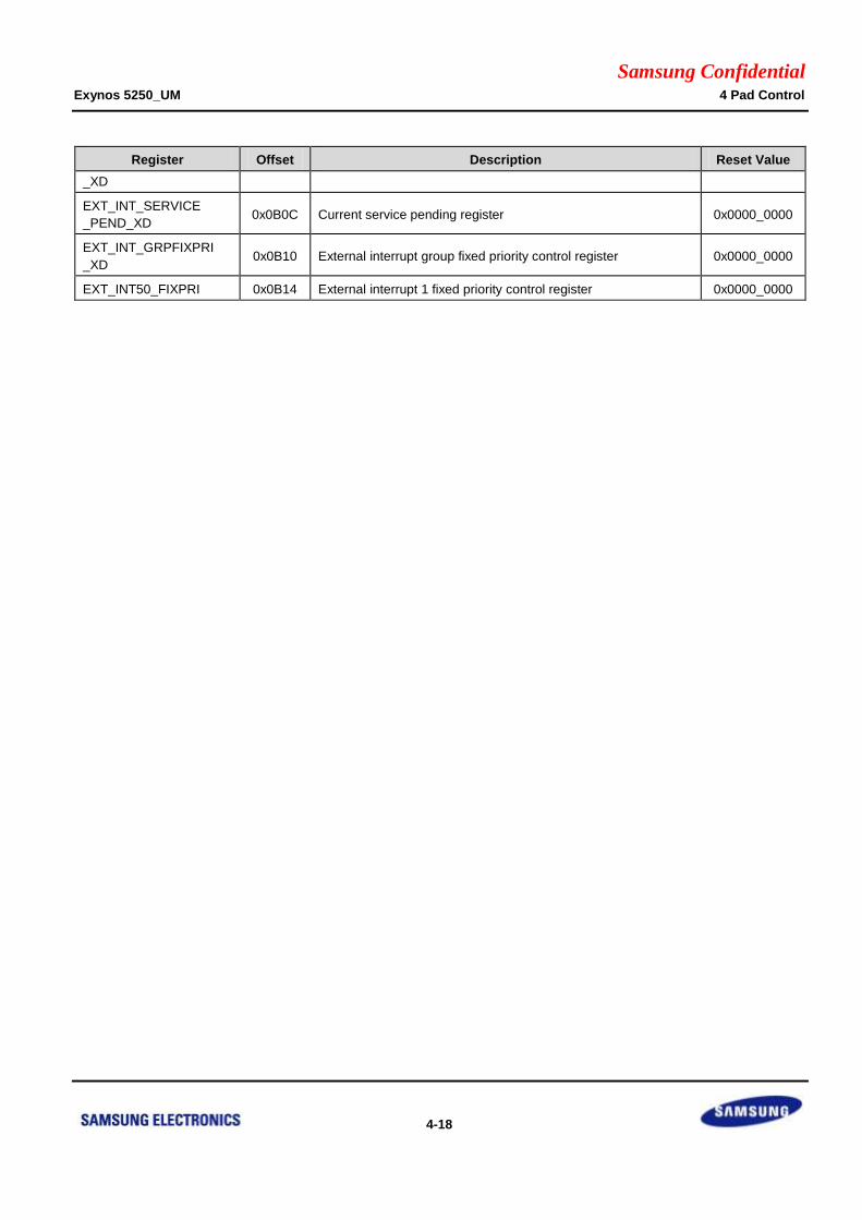
Samsung Confidential Exynos 5250_UM 4 Pad Control
4-18
Register Offset Description Reset Value
_XD
EXT_INT_SERVICE
_PEND_XD 0x0B0C Current service pending register 0x0000_0000
EXT_INT_GRPFIXPRI
_XD 0x0B10 External interrupt group fixed priority control register 0x0000_0000
EXT_INT50_FIXPRI 0x0B14 External interrupt 1 fixed priority control register 0x0000_0000

Samsung Confidential Exynos 5250_UM 4 Pad Control
4-19
4.4.1.1 GPA0CON
Base Address: 0x1140_0000
Address = Base Address + 0x0000, Reset Value = 0x0000_0000
Name Bit Type Description Reset Value
GPA0CON[7] [31:28] RW
0x0 = Input
0x1 = Output
0x2 = Reserved
0x3 = I2C_2_SCL
0x4 = HS-I2C_2_SCL
0x5 to 0xE = Reserved
0xF = EXT_INT1[7]
0x00
GPA0CON[6] [27:24] RW
0x0 = Input
0x1 = Output
0x2 = Reserved
0x3 = I2C_2_SDA
0x4 = HS-I2C_2_SDA
0x5 to 0xE = Reserved
0xF = EXT_INT1[6]
0x00
GPA0CON[5] [23:20] RW
0x0 = Input
0x1 = Output
0x2 to 0xE = Reserved
0xF = EXT_INT1[5]
0x00
GPA0CON[4] [19:16] RW
0x0 = Input
0x1 = Output
0x2 to 0xE = Reserved
0xF = EXT_INT1[4]
0x00
GPA0CON[3] [15:12] RW
0x0 = Input
0x1 = Output
0x2 = UART_0_RTSn
0x3 to 0xE = Reserved
0xF = EXT_INT1[3]
0x00
GPA0CON[2] [11:8] RW
0x0 = Input
0x1 = Output
0x2 = UART_0_CTSn
0x3 to 0xE = Reserved
0xF = EXT_INT1[2]
0x00
GPA0CON[1] [7:4] RW
0x0 = Input
0x1 = Output
0x2 = UART_0_TXD
0x3 to 0xE = Reserved
0xF = EXT_INT1[1]
0x00
GPA0CON[0] [3:0] RW
0x0 = Input
0x1 = Output
0x2 = UART_0_RXD
0x3 to 0xE = Reserved
0xF = EXT_INT1[0]
0x00

Samsung Confidential Exynos 5250_UM 4 Pad Control
4-20
4.4.1.2 GPA0DAT
Base Address: 0x1140_0000
Address = Base Address + 0x0004, Reset Value = 0x00
Name Bit Type Description Reset Value
GPA0DAT[7:0] [7:0] RWX
When you configure the port as input port, the
corresponding bit is the pin state. When you configure
the port as output port, the pin state is similar as the
corresponding bit. When you configure the port as
functional pin, you can read the undefined value.
0x00
4.4.1.3 GPA0PUD
Base Address: 0x1140_0000
Address = Base Address + 0x0008, Reset Value = 0x5555
Name Bit Type Description Reset Value
GPA0PUD[n] [2n + 1:2n]
n = 0 to 7 RW
0x0 = Disables Pull-up/down
0x1 = Enables Pull-down
0x2 = Reserved
0x3 = Enables Pull-up
0x5555
4.4.1.4 GPA0DRV
Base Address: 0x1140_0000
Address = Base Address + 0x000C, Reset Value = 0x00_0000
Name Bit Type Description Reset Value
GPA0DRV[n]
[2n + 1:2n]
n = 0 to 7 RW
0x0 = 1x
0x2 = 2x
0x1 = 3x
0x3 = 4x
0x00_0000
[n + 16:16]
n = 0 to 7 RW Reserved. Should be zero. 0x00_0000

Samsung Confidential Exynos 5250_UM 4 Pad Control
4-21
4.4.1.5 GPA0CONPDN
Base Address: 0x1140_0000
Address = Base Address + 0x0010, Reset Value = 0x0000
Name Bit Type Description Reset Value
GPA0[n] [2n + 1:2n]
n = 0 to 7 RW
0x0 = Output 0
0x1 = Output 1
0x2 = Input
0x3 = Previous state
0x00
4.4.1.6 GPA0PUDPDN
Base Address: 0x1140_0000
Address = Base Address + 0x0014, Reset Value = 0x0000
Name Bit Type Description Reset Value
GPA0[n] [2n + 1:2n]
n = 0 to 7 RW
0x0 = Disables Pull-up/down
0x1 = Enables Pull-down
0x2 = Reserved
0x3 = Enables Pull-up
0x00
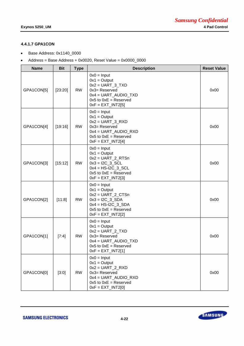
Samsung Confidential Exynos 5250_UM 4 Pad Control
4-22
4.4.1.7 GPA1CON
Base Address: 0x1140_0000
Address = Base Address + 0x0020, Reset Value = 0x0000_0000
Name Bit Type Description Reset Value
GPA1CON[5] [23:20] RW
0x0 = Input
0x1 = Output
0x2 = UART_3_TXD
0x3= Reserved
0x4 = UART_AUDIO_TXD
0x5 to 0xE = Reserved
0xF = EXT_INT2[5]
0x00
GPA1CON[4] [19:16] RW
0x0 = Input
0x1 = Output
0x2 = UART_3_RXD
0x3= Reserved
0x4 = UART_AUDIO_RXD
0x5 to 0xE = Reserved
0xF = EXT_INT2[4]
0x00
GPA1CON[3] [15:12] RW
0x0 = Input
0x1 = Output
0x2 = UART_2_RTSn
0x3 = I2C_3_SCL
0x4 = HS-I2C_3_SCL
0x5 to 0xE = Reserved
0xF = EXT_INT2[3]
0x00
GPA1CON[2] [11:8] RW
0x0 = Input
0x1 = Output
0x2 = UART_2_CTSn
0x3 = I2C_3_SDA
0x4 = HS-I2C_3_SDA
0x5 to 0xE = Reserved
0xF = EXT_INT2[2]
0x00
GPA1CON[1] [7:4] RW
0x0 = Input
0x1 = Output
0x2 = UART_2_TXD
0x3= Reserved
0x4 = UART_AUDIO_TXD
0x5 to 0xE = Reserved
0xF = EXT_INT2[1]
0x00
GPA1CON[0] [3:0] RW
0x0 = Input
0x1 = Output
0x2 = UART_2_RXD
0x3= Reserved
0x4 = UART_AUDIO_RXD
0x5 to 0xE = Reserved
0xF = EXT_INT2[0]
0x00

Samsung Confidential Exynos 5250_UM 4 Pad Control
4-23
4.4.1.8 GPA1DAT
Base Address: 0x1140_0000
Address = Base Address + 0x0024, Reset Value = 0x00
Name Bit Type Description Reset Value
GPA1DAT[5:0] [5:0] RWX
When you configure the port as input port, the
corresponding bit is the pin state. When you configure
the port as output port, the pin state is similar as the
corresponding bit. When you configure the port as
functional pin, the undefined value will be read.
0x00
4.4.1.9 GPA1PUD
Base Address: 0x1140_0000
Address = Base Address + 0x0028, Reset Value = 0x0555
Name Bit Type Description Reset Value
GPA1PUD[n] [2n + 1:2n]
n = 0 to 5 RW
0x0 = Disables Pull-up/down
0x1 = Enables Pull-down
0x2 = Reserved
0x3 = Enables Pull-up
0x0555
4.4.1.10 GPA1DRV
Base Address: 0x1140_0000
Address = Base Address + 0x002C, Reset Value = 0x00_0000
Name Bit Type Description Reset Value
GPA1DRV[n]
[2n + 1:2n]
n = 0 to 5 RW
0x0 = 1x
0x2 = 2x
0x1 = 3x
0x3 = 4x
0x00_0000
[n + 16:16]
n = 0 to 5 RW Reserved. Should be zero. 0x00_0000

Samsung Confidential Exynos 5250_UM 4 Pad Control
4-24
4.4.1.11 GPA1CONPDN
Base Address: 0x1140_0000
Address = Base Address + 0x0030, Reset Value = 0x0000
Name Bit Type Description Reset Value
GPA1[n] [2n + 1:2n]
n = 0 to 5 RW
0x0 = Output 0
0x1 = Output 1
0x2 = Input
0x3 = Previous state
0x00
4.4.1.12 GPA1PUDPDN
Base Address: 0x1140_0000
Address = Base Address + 0x0034, Reset Value = 0x0000
Name Bit Type Description Reset Value
GPA1[n] [2n + 1:2n]
n = 0 to 5 RW
0x0 = Disables Pull-up/down
0x1 = Enables Pull-down
0x2 = Reserved
0x3 = Enables Pull-up
0x00

Samsung Confidential Exynos 5250_UM 4 Pad Control
4-25
4.4.1.13 GPA2CON
Base Address: 0x1140_0000
Address = Base Address + 0x0040, Reset Value = 0x0000_0000
Name Bit Type Description Reset Value
GPA2CON[7] [31:28] RW
0x0 = Input
0x1 = Output
0x2 = SPI_1_MOSI
0x3 to 0xE = Reserved
0xF = EXT_INT3[7]
0x00
GPA2CON[6] [27:24] RW
0x0 = Input
0x1 = Output
0x2 = SPI_1_MISO
0x3 to 0xE = Reserved
0xF = EXT_INT3[6]
0x00
GPA2CON[5] [23:20] RW
0x0 = Input
0x1 = Output
0x2 = SPI_1_nSS
0x3 = Reserved
0x4 = Reserved
0x5 to 0xE = Reserved
0xF = EXT_INT3[5]
0x00
GPA2CON[4] [19:16] RW
0x0 = Input
0x1 = Output
0x2 = SPI_1_CLK
0x3 = Reserved
0x4 = Reserved
0x5 to 0xE = Reserved
0xF = EXT_INT3[4]
0x00
GPA2CON[3] [15:12] RW
0x0 = Input
0x1 = Output
0x2 = SPI_0_MOSI
0x3 = I2C_5_SCL
0x4 to 0xE = Reserved
0xF = EXT_INT3[3]
0x00
GPA2CON[2] [11:8] RW
0x0 = Input
0x1 = Output
0x2 = SPI_0_MISO
0x3 = I2C_5_SDA
0x4 to 0xE = Reserved
0xF = EXT_INT3[2]
0x00
GPA2CON[1] [7:4] RW
0x0 = Input
0x1 = Output
0x2 = SPI_0_nSS
0x3 = I2C_4_SCL
0x4 to 0xE = Reserved
0xF = EXT_INT3[1]
0x00
GPA2CON[0] [3:0] RW 0x0 = Input
0x1 = Output 0x00
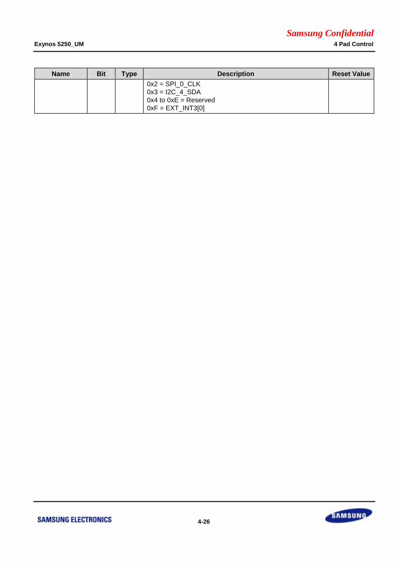
Samsung Confidential Exynos 5250_UM 4 Pad Control
4-26
Name Bit Type Description Reset Value
0x2 = SPI_0_CLK
0x3 = I2C_4_SDA
0x4 to 0xE = Reserved
0xF = EXT_INT3[0]

Samsung Confidential Exynos 5250_UM 4 Pad Control
4-27
4.4.1.14 GPA2DAT
Base Address: 0x1140_0000
Address = Base Address + 0x0044, Reset Value = 0x00
Name Bit Type Description Reset Value
GPA2DAT[7:0] [7:0] RWX
When you configure the port as input port, the
corresponding bit is the pin state. When you configure
the port as output port, the pin state is the same as the
corresponding bit. When you configure the port as
functional pin, the undefined value will be read.
0x00
4.4.1.15 GPA2PUD
Base Address: 0x1140_0000
Address = Base Address + 0x0048, Reset Value = 0x5555
Name Bit Type Description Reset Value
GPA2PUD[n] [2n + 1:2n]
n = 0 to 7 RW
0x0 = Disables Pull-up/down
0x1 = Enables Pull-down
0x2 = Reserved
0x3 = Enables Pull-up
0x5555
4.4.1.16 GPA2DRV
Base Address: 0x1140_0000
Address = Base Address + 0x004C, Reset Value = 0x00_0000
Name Bit Type Description Reset Value
GPA2DRV[n]
[2n + 1:2n]
n = 0 to 7 RW
0x0 = 1x
0x2 = 2x
0x1 = 3x
0x3 = 4x
0x00_0000
[n + 16:16]
n = 0 to 7 RW Reserved. Should be zero. 0x00_0000

Samsung Confidential Exynos 5250_UM 4 Pad Control
4-28
4.4.1.17 GPA2CONPDN
Base Address: 0x1140_0000
Address = Base Address + 0x0050, Reset Value = 0x0000
Name Bit Type Description Reset Value
GPA2[n] [2n + 1:2n]
n = 0 to 7 RW
0x0 = Output 0
0x1 = Output 1
0x2 = Input
0x3 = Previous state
0x00
4.4.1.18 GPA2PUDPDN
Base Address: 0x1140_0000
Address = Base Address + 0x0054, Reset Value = 0x0000
Name Bit Type Description Reset Value
GPA2[n] [2n + 1:2n]
n = 0 to 7 RW
0x0 = Disables Pull-up/down
0x1 = Enables Pull-down
0x2 = Reserved
0x3 = Enables Pull-up
0x00
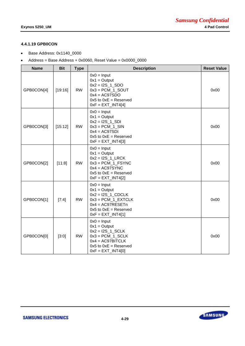
Samsung Confidential Exynos 5250_UM 4 Pad Control
4-29
4.4.1.19 GPB0CON
Base Address: 0x1140_0000
Address = Base Address + 0x0060, Reset Value = 0x0000_0000
Name Bit Type Description Reset Value
GPB0CON[4] [19:16] RW
0x0 = Input
0x1 = Output
0x2 = I2S_1_SDO
0x3 = PCM_1_SOUT
0x4 = AC97SDO
0x5 to 0xE = Reserved
0xF = EXT_INT4[4]
0x00
GPB0CON[3] [15:12] RW
0x0 = Input
0x1 = Output
0x2 = I2S_1_SDI
0x3 = PCM_1_SIN
0x4 = AC97SDI
0x5 to 0xE = Reserved
0xF = EXT_INT4[3]
0x00
GPB0CON[2] [11:8] RW
0x0 = Input
0x1 = Output
0x2 = I2S_1_LRCK
0x3 = PCM_1_FSYNC
0x4 = AC97SYNC
0x5 to 0xE = Reserved
0xF = EXT_INT4[2]
0x00
GPB0CON[1] [7:4] RW
0x0 = Input
0x1 = Output
0x2 = I2S_1_CDCLK
0x3 = PCM_1_EXTCLK
0x4 = AC97RESETn
0x5 to 0xE = Reserved
0xF = EXT_INT4[1]
0x00
GPB0CON[0] [3:0] RW
0x0 = Input
0x1 = Output
0x2 = I2S_1_SCLK
0x3 = PCM_1_SCLK
0x4 = AC97BITCLK
0x5 to 0xE = Reserved
0xF = EXT_INT4[0]
0x00

Samsung Confidential Exynos 5250_UM 4 Pad Control
4-30
4.4.1.20 GPB0DAT
Base Address: 0x1140_0000
Address = Base Address + 0x0064, Reset Value = 0x00
Name Bit Type Description Reset Value
GPB0DAT[4:0] [4:0] RWX
When you configure the port as input port, the
corresponding bit is the pin state. When you configure
the port as output port, the pin state is the same as the
corresponding bit. When you configure the port as
functional pin, the undefined value will be read.
0x00
4.4.1.21 GPB0PUD
Base Address: 0x1140_0000
Address = Base Address + 0x0068, Reset Value = 0x0155
Name Bit Type Description Reset Value
GPB0PUD[n] [2n + 1:2n]
n = 0 to 4 RW
0x0 = Disables Pull-up/down
0x1 = Enables Pull-down
0x2 = Reserved
0x3 = Enables Pull-up
0x0155
4.4.1.22 GPB0DRV
Base Address: 0x1140_0000
Address = Base Address + 0x006C, Reset Value = 0x00_0000
Name Bit Type Description Reset Value
GPB0DRV[n]
[2n + 1:2n]
n = 0 to 4 RW
0x0 = 1x
0x2 = 2x
0x1 = 3x
0x3 = 4x
0x00_0000
[n + 16:16]
n = 0 to 4 RW Reserved. Should be zero. 0x00_0000

Samsung Confidential Exynos 5250_UM 4 Pad Control
4-31
4.4.1.23 GPB0CONPDN
Base Address: 0x1140_0000
Address = Base Address + 0x0070, Reset Value = 0x0000
Name Bit Type Description Reset Value
GPB0[n] [2n + 1:2n]
n = 0 to 4 RW
0x0 = Output 0
0x1 = Output 1
0x2 = Input
0x3 = Previous state
0x00
4.4.1.24 GPB0PUDPDN
Base Address: 0x1140_0000
Address = Base Address + 0x0074, Reset Value = 0x0000
Name Bit Type Description Reset Value
GPB0[n] [2n + 1:2n]
n = 0 to 4 RW
0x0 = Disables Pull-up/down
0x1 = Enables Pull-down
0x2 = Reserved
0x3 = Enables Pull-up
0x00
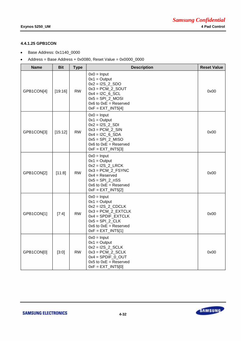
Samsung Confidential Exynos 5250_UM 4 Pad Control
4-32
4.4.1.25 GPB1CON
Base Address: 0x1140_0000
Address = Base Address + 0x0080, Reset Value = 0x0000_0000
Name Bit Type Description Reset Value
GPB1CON[4] [19:16] RW
0x0 = Input
0x1 = Output
0x2 = I2S_2_SDO
0x3 = PCM_2_SOUT
0x4 = I2C_6_SCL
0x5 = SPI_2_MOSI
0x6 to 0xE = Reserved
0xF = EXT_INT5[4]
0x00
GPB1CON[3] [15:12] RW
0x0 = Input
0x1 = Output
0x2 = I2S_2_SDI
0x3 = PCM_2_SIN
0x4 = I2C_6_SDA
0x5 = SPI_2_MISO
0x6 to 0xE = Reserved
0xF = EXT_INT5[3]
0x00
GPB1CON[2] [11:8] RW
0x0 = Input
0x1 = Output
0x2 = I2S_2_LRCK
0x3 = PCM_2_FSYNC
0x4 = Reserved
0x5 = SPI_2_nSS
0x6 to 0xE = Reserved
0xF = EXT_INT5[2]
0x00
GPB1CON[1] [7:4] RW
0x0 = Input
0x1 = Output
0x2 = I2S_2_CDCLK
0x3 = PCM_2_EXTCLK
0x4 = SPDIF_EXTCLK
0x5 = SPI_2_CLK
0x6 to 0xE = Reserved
0xF = EXT_INT5[1]
0x00
GPB1CON[0] [3:0] RW
0x0 = Input
0x1 = Output
0x2 = I2S_2_SCLK
0x3 = PCM_2_SCLK
0x4 = SPDIF_0_OUT
0x5 to 0xE = Reserved
0xF = EXT_INT5[0]
0x00

Samsung Confidential Exynos 5250_UM 4 Pad Control
4-33
4.4.1.26 GPB1DAT
Base Address: 0x1140_0000
Address = Base Address + 0x0084, Reset Value = 0x00
Name Bit Type Description Reset Value
GPB1DAT[4:0] [4:0] RWX
When you configure the port as input port, the
corresponding bit is the pin state. When you configure
the port as output port, the pin state is the same as the
corresponding bit. When you configure the port as
functional pin, the undefined value will be read.
0x00
4.4.1.27 GPB1PUD
Base Address: 0x1140_0000
Address = Base Address + 0x0088, Reset Value = 0x0155
Name Bit Type Description Reset Value
GPB1PUD[n] [2n + 1:2n]
n = 0 to 4 RW
0x0 = Disables Pull-up/down
0x1 = Enables Pull-down
0x2 = Reserved
0x3 = Enables Pull-up
0x0155
4.4.1.28 GPB1DRV
Base Address: 0x1140_0000
Address = Base Address + 0x008C, Reset Value = 0x00_0000
Name Bit Type Description Reset Value
GPB1DRV[n]
[2n + 1:2n]
n = 0 to 4 RW
0x0 = 1x
0x2 = 2x
0x1 = 3x
0x3 = 4x
0x00_0000
[n + 16:16]
n = 0 to 4 RW Reserved. Should be zero. 0x00_0000

Samsung Confidential Exynos 5250_UM 4 Pad Control
4-34
4.4.1.29 GPB1CONPDN
Base Address: 0x1140_0000
Address = Base Address + 0x0090, Reset Value = 0x0000
Name Bit Type Description Reset Value
GPB1[n] [2n + 1:2n]
n = 0 to 4 RW
0x0 = Output 0
0x1 = Output 1
0x2 = Input
0x3 = Previous state
0x00
4.4.1.30 GPB1PUDPDN
Base Address: 0x1140_0000
Address = Base Address + 0x0094, Reset Value = 0x0000
Name Bit Type Description Reset Value
GPB1[n] [2n + 1:2n]
n = 0 to 4 RW
0x0 = Disables Pull-up/down
0x1 = Enables Pull-down
0x2 = Reserved
0x3 = Enables Pull-up
0x00
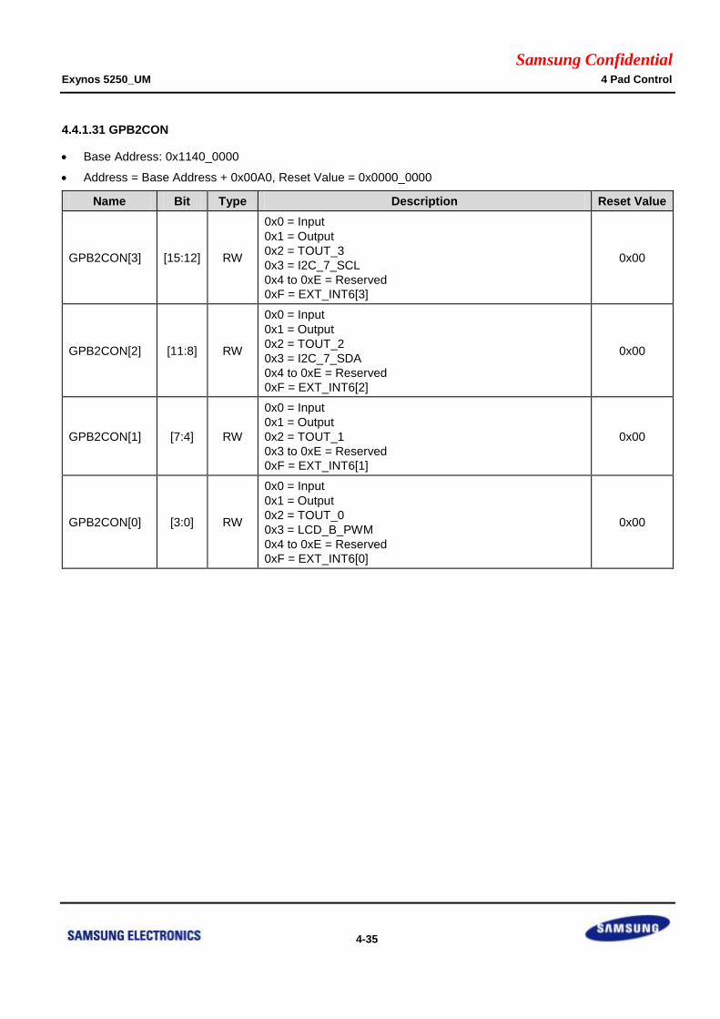
Samsung Confidential Exynos 5250_UM 4 Pad Control
4-35
4.4.1.31 GPB2CON
Base Address: 0x1140_0000
Address = Base Address + 0x00A0, Reset Value = 0x0000_0000
Name Bit Type Description Reset Value
GPB2CON[3] [15:12] RW
0x0 = Input
0x1 = Output
0x2 = TOUT_3
0x3 = I2C_7_SCL
0x4 to 0xE = Reserved
0xF = EXT_INT6[3]
0x00
GPB2CON[2] [11:8] RW
0x0 = Input
0x1 = Output
0x2 = TOUT_2
0x3 = I2C_7_SDA
0x4 to 0xE = Reserved
0xF = EXT_INT6[2]
0x00
GPB2CON[1] [7:4] RW
0x0 = Input
0x1 = Output
0x2 = TOUT_1
0x3 to 0xE = Reserved
0xF = EXT_INT6[1]
0x00
GPB2CON[0] [3:0] RW
0x0 = Input
0x1 = Output
0x2 = TOUT_0
0x3 = LCD_B_PWM
0x4 to 0xE = Reserved
0xF = EXT_INT6[0]
0x00
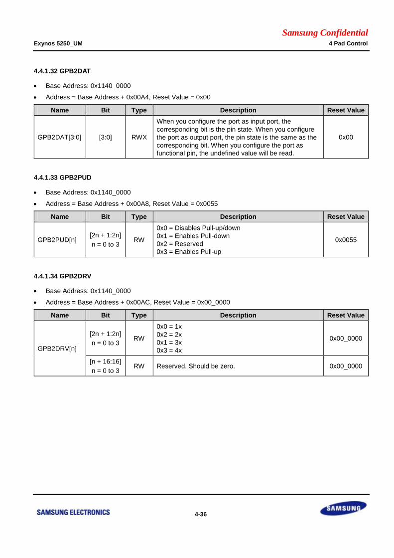
Samsung Confidential Exynos 5250_UM 4 Pad Control
4-36
4.4.1.32 GPB2DAT
Base Address: 0x1140_0000
Address = Base Address + 0x00A4, Reset Value = 0x00
Name Bit Type Description Reset Value
GPB2DAT[3:0] [3:0] RWX
When you configure the port as input port, the
corresponding bit is the pin state. When you configure
the port as output port, the pin state is the same as the
corresponding bit. When you configure the port as
functional pin, the undefined value will be read.
0x00
4.4.1.33 GPB2PUD
Base Address: 0x1140_0000
Address = Base Address + 0x00A8, Reset Value = 0x0055
Name Bit Type Description Reset Value
GPB2PUD[n] [2n + 1:2n]
n = 0 to 3 RW
0x0 = Disables Pull-up/down
0x1 = Enables Pull-down
0x2 = Reserved
0x3 = Enables Pull-up
0x0055
4.4.1.34 GPB2DRV
Base Address: 0x1140_0000
Address = Base Address + 0x00AC, Reset Value = 0x00_0000
Name Bit Type Description Reset Value
GPB2DRV[n]
[2n + 1:2n]
n = 0 to 3 RW
0x0 = 1x
0x2 = 2x
0x1 = 3x
0x3 = 4x
0x00_0000
[n + 16:16]
n = 0 to 3 RW Reserved. Should be zero. 0x00_0000

Samsung Confidential Exynos 5250_UM 4 Pad Control
4-37
4.4.1.35 GPB2CONPDN
Base Address: 0x1140_0000
Address = Base Address + 0x00B0, Reset Value = 0x0000
Name Bit Type Description Reset Value
GPB2[n] [2n + 1:2n]
n = 0 to 3 RW
0x0 = Output 0
0x1 = Output 1
0x2 = Input
0x3 = Previous state
0x00
4.4.1.36 GPB2PUDPDN
Base Address: 0x1140_0000
Address = Base Address + 0x00B4, Reset Value = 0x0000
Name Bit Type Description Reset Value
GPB2[n] [2n + 1:2n]
n = 0 to 3 RW
0x0 = Disables Pull-up/down
0x1 = Enables Pull-down
0x2 = Reserved
0x3 = Enables Pull-up
0x00
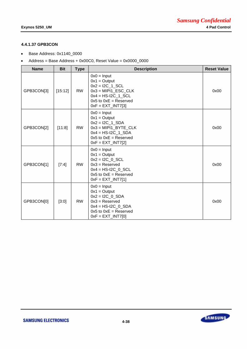
Samsung Confidential Exynos 5250_UM 4 Pad Control
4-38
4.4.1.37 GPB3CON
Base Address: 0x1140_0000
Address = Base Address + 0x00C0, Reset Value = 0x0000_0000
Name Bit Type Description Reset Value
GPB3CON[3] [15:12] RW
0x0 = Input
0x1 = Output
0x2 = I2C_1_SCL
0x3 = MIPI1_ESC_CLK
0x4 = HS-I2C_1_SCL
0x5 to 0xE = Reserved
0xF = EXT_INT7[3]
0x00
GPB3CON[2] [11:8] RW
0x0 = Input
0x1 = Output
0x2 = I2C_1_SDA
0x3 = MIPI1_BYTE_CLK
0x4 = HS-I2C_1_SDA
0x5 to 0xE = Reserved
0xF = EXT_INT7[2]
0x00
GPB3CON[1] [7:4] RW
0x0 = Input
0x1 = Output
0x2 = I2C_0_SCL
0x3 = Reserved
0x4 = HS-I2C_0_SCL
0x5 to 0xE = Reserved
0xF = EXT_INT7[1]
0x00
GPB3CON[0] [3:0] RW
0x0 = Input
0x1 = Output
0x2 = I2C_0_SDA
0x3 = Reserved
0x4 = HS-I2C_0_SDA
0x5 to 0xE = Reserved
0xF = EXT_INT7[0]
0x00

Samsung Confidential Exynos 5250_UM 4 Pad Control
4-39
4.4.1.38 GPB3DAT
Base Address: 0x1140_0000
Address = Base Address + 0x00C4, Reset Value = 0x00
Name Bit Type Description Reset Value
GPB3DAT[3:0] [3:0] RWX
When you configure the port as input port, the
corresponding bit is the pin state. When you configure
the port as output port, the pin state is the same as the
corresponding bit. When you configure the port as
functional pin, the undefined value will be read.
0x00
4.4.1.39 GPB3PUD
Base Address: 0x1140_0000
Address = Base Address + 0x00C8, Reset Value = 0x0055
Name Bit Type Description Reset Value
GPB3PUD[n] [2n + 1:2n]
n = 0 to 3 RW
0x0 = Disables Pull-up/down
0x1 = Enables Pull-down
0x2 = Reserved
0x3 = Enables Pull-up
0x0055
4.4.1.40 GPB3DRV
Base Address: 0x1140_0000
Address = Base Address + 0x00CC, Reset Value = 0x00_0000
Name Bit Type Description Reset Value
GPB3DRV[n]
[2n + 1:2n]
n = 0 to 3 RW
0x0 = 1x
0x2 = 2x
0x1 = 3x
0x3 = 4x
0x00_0000
[n + 16:16]
n = 0 to 3 RW Reserved. Should be zero. 0x00_0000

Samsung Confidential Exynos 5250_UM 4 Pad Control
4-40
4.4.1.41 GPB3CONPDN
Base Address: 0x1140_0000
Address = Base Address + 0x00D0, Reset Value = 0x0000
Name Bit Type Description Reset Value
GPB3[n] [2n + 1:2n]
n = 0 to 3 RW
0x0 = Output 0
0x1 = Output 1
0x2 = Input
0x3 = Previous state
0x00
4.4.1.42 GPB3PUDPDN
Base Address: 0x1140_0000
Address = Base Address + 0x00D4, Reset Value = 0x0000
Name Bit Type Description Reset Value
GPB3[n] [2n + 1:2n]
n = 0 to 3 RW
0x0 = Disables Pull-up/down
0x1 = Enables Pull-down
0x2 = Reserved
0x3 = Enables Pull-up
0x00

Samsung Confidential Exynos 5250_UM 4 Pad Control
4-41
4.4.1.43 GPC0CON
Base Address: 0x1140_0000
Address = Base Address + 0x00E0, Reset Value = 0x0000_0000
Name Bit Type Description Reset Value
GPC0CON[6] [27:24] RW
0x0 = Input
0x1 = Output
0x2 = SD_0_DATA[3]
0x3 to 0xE = Reserved
0xF = EXT_INT8[6]
0x00
GPC0CON[5] [23:20] RW
0x0 = Input
0x1 = Output
0x2 = SD_0_DATA[2]
0x3 to 0xE = Reserved
0xF = EXT_INT8[5]
0x00
GPC0CON[4] [19:16] RW
0x0 = Input
0x1 = Output
0x2 = SD_0_DATA[1]
0x3 to 0xE = Reserved
0xF = EXT_INT8[4]
0x00
GPC0CON[3] [15:12] RW
0x0 = Input
0x1 = Output
0x2 = SD_0_DATA[0]
0x3 to 0xE = Reserved
0xF = EXT_INT8[3]
0x00
GPC0CON[2] [11:8] RW
0x0 = Input
0x1 = Output
0x2 = SD_0_CDn
0x3 = SD_4_ nRESET_OUT
0x4 = SD_0_CARD_INT_n
0x5 to 0xE = Reserved
0xF = EXT_INT8[2]
0x00
GPC0CON[1] [7:4] RW
0x0 = Input
0x1 = Output
0x2 = SD_0_CMD
0x3 to 0xE = Reserved
0xF = EXT_INT8[1]
0x00
GPC0CON[0] [3:0] RW
0x0 = Input
0x1 = Output
0x2 = SD_0_CLK
0x3 to 0xE = Reserved
0xF = EXT_INT8[0]
0x00

Samsung Confidential Exynos 5250_UM 4 Pad Control
4-42
4.4.1.44 GPC0DAT
Base Address: 0x1140_0000
Address = Base Address + 0x00E4, Reset Value = 0x00
Name Bit Type Description Reset Value
GPC0DAT[6:0] [6:0] RWX
When you configure the port as input port, the
corresponding bit is the pin state. When you configure
the port as output port, the pin state is the same as the
corresponding bit. When you configure the port as
functional pin, the undefined value will be read.
0x00
4.4.1.45 GPC0PUD
Base Address: 0x1140_0000
Address = Base Address + 0x00E8, Reset Value = 0x1555
Name Bit Type Description Reset Value
GPC0PUD[n] [2n + 1:2n]
n = 0 to 6 RW
0x0 = Disables Pull-up/down
0x1 = Enables Pull-down
0x2 = Reserved
0x3 = Enables Pull-up
0x1555
4.4.1.46 GPC0DRV
Base Address: 0x1140_0000
Address = Base Address + 0x00EC, Reset Value = 0x00_2AAA
Name Bit Type Description Reset Value
GPC0DRV[n]
[2n + 1:2n]
n = 0 to 6 RW
0x0 = 1x
0x2 = 2x
0x1 = 3x
0x3 = 4x
0x00_2AAA
[n + 16:16]
n = 0 to 6 RW Reserved. Should be zero. 0x00_0000
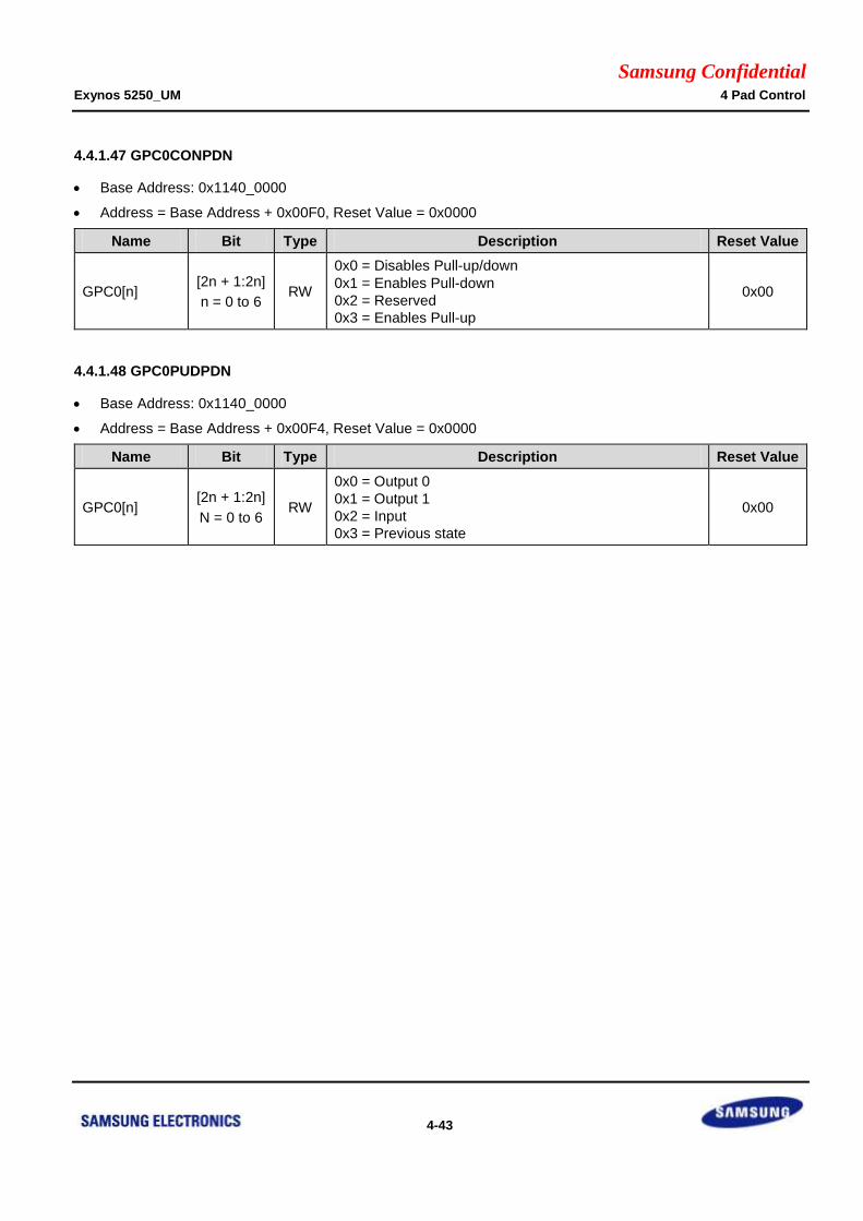
Samsung Confidential Exynos 5250_UM 4 Pad Control
4-43
4.4.1.47 GPC0CONPDN
Base Address: 0x1140_0000
Address = Base Address + 0x00F0, Reset Value = 0x0000
Name Bit Type Description Reset Value
GPC0[n] [2n + 1:2n]
n = 0 to 6 RW
0x0 = Disables Pull-up/down
0x1 = Enables Pull-down
0x2 = Reserved
0x3 = Enables Pull-up
0x00
4.4.1.48 GPC0PUDPDN
Base Address: 0x1140_0000
Address = Base Address + 0x00F4, Reset Value = 0x0000
Name Bit Type Description Reset Value
GPC0[n] [2n + 1:2n]
N = 0 to 6 RW
0x0 = Output 0
0x1 = Output 1
0x2 = Input
0x3 = Previous state
0x00

Samsung Confidential Exynos 5250_UM 4 Pad Control
4-44
4.4.1.49 GPC1CON
Base Address: 0x1140_0000
Address = Base Address + 0x0100, Reset Value = 0x0000_0000
Name Bit Type Description Reset Value
GPC1CON[3] [15:12] RW
0x0 = Input
0x1 = Output
0x2 = SD_0_DATA[7],
0x3 to 0xE = Reserved
0xF = EXT_INT9[3]
0x00
GPC1CON[2] [11:8] RW
0x0 = Input
0x1 = Output
0x2 = SD_0_DATA[6],
0x3 to 0xE = Reserved
0xF = EXT_INT9[2]
0x00
GPC1CON[1] [7:4] RW
0x0 = Input
0x1 = Output
0x2 = SD_0_DATA[5]
0x3 to 0xE = Reserved
0xF = EXT_INT9[1]
0x00
GPC1CON[0] [3:0] RW
0x0 = Input
0x1 = Output
0x2 = SD_0_DATA[4]
0x3 to 0xE = Reserved
0xF = EXT_INT9[0]
0x00

Samsung Confidential Exynos 5250_UM 4 Pad Control
4-45
4.4.1.50 GPC1DAT
Base Address: 0x1140_0000
Address = Base Address + 0x0104, Reset Value = 0x00
Name Bit Type Description Reset Value
GPC1DAT[3:0] [3:0] RWX
When you configure the port as input port, the
corresponding bit is the pin state. When you configure
the port as output port, the pin state is the same as the
corresponding bit. When you configure the port as
functional pin, you can read the undefined value.
0x00
4.4.1.51 GPC1PUD
Base Address: 0x1140_0000
Address = Base Address + 0x0108, Reset Value = 0x0055
Name Bit Type Description Reset Value
GPC1PUD[n] [2n + 1:2n]
n = 0 to 3 RW
0x0 = Disables Pull-up/down
0x1 = Enables Pull-down
0x2 = Reserved
0x3 = Enables Pull-up
0x0055
4.4.1.52 GPC1DRV
Base Address: 0x1140_0000
Address = Base Address + 0x010C, Reset Value = 0x00_0000
Name Bit Type Description Reset Value
GPC1DRV[n]
[2n + 1:2n]
n = 0 to 3 RW
0x0 = 1x
0x2 = 2x
0x1 = 3x
0x3 = 4x
0x00_0000
[n + 16:16]
n = 0 to 3 RW Reserved. Should be zero. 0x00_0000

Samsung Confidential Exynos 5250_UM 4 Pad Control
4-46
4.4.1.53 GPC1CONPDN
Base Address: 0x1140_0000
Address = Base Address + 0x0110, Reset Value = 0x0000
Name Bit Type Description Reset Value
GPC1[n] [2n + 1:2n]
n = 0 to 3 RW
0x0 = Output 0
0x1 = Output 1
0x2 = Input
0x3 = Previous state
0x00
4.4.1.54 GPC1PUDPDN
Base Address: 0x1140_0000
Address = Base Address + 0x0114, Reset Value = 0x0000
Name Bit Type Description Reset Value
GPC1[n] [2n + 1:2n]
n = 0 to 3 RW
0x0 = Disables Pull-up/down
0x1 = Enables Pull-down
0x2 = Reserved
0x3 = Enables Pull-up
0x00
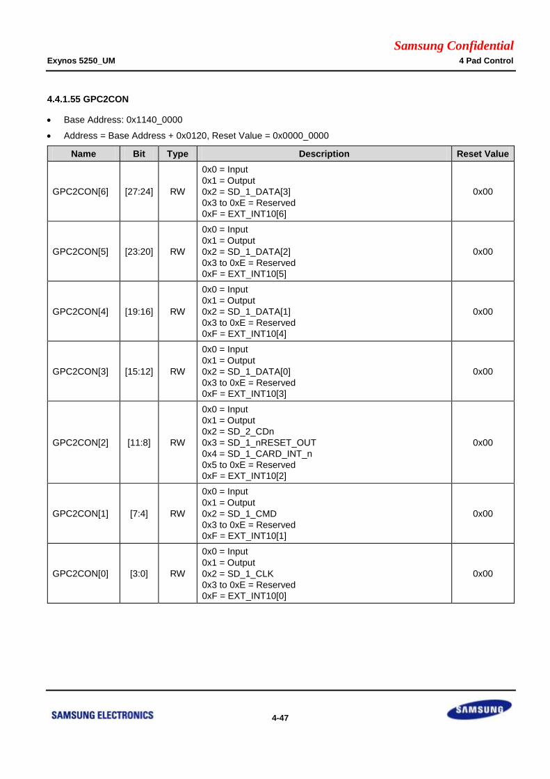
Samsung Confidential Exynos 5250_UM 4 Pad Control
4-47
4.4.1.55 GPC2CON
Base Address: 0x1140_0000
Address = Base Address + 0x0120, Reset Value = 0x0000_0000
Name Bit Type Description Reset Value
GPC2CON[6] [27:24] RW
0x0 = Input
0x1 = Output
0x2 = SD_1_DATA[3]
0x3 to 0xE = Reserved
0xF = EXT_INT10[6]
0x00
GPC2CON[5] [23:20] RW
0x0 = Input
0x1 = Output
0x2 = SD_1_DATA[2]
0x3 to 0xE = Reserved
0xF = EXT_INT10[5]
0x00
GPC2CON[4] [19:16] RW
0x0 = Input
0x1 = Output
0x2 = SD_1_DATA[1]
0x3 to 0xE = Reserved
0xF = EXT_INT10[4]
0x00
GPC2CON[3] [15:12] RW
0x0 = Input
0x1 = Output
0x2 = SD_1_DATA[0]
0x3 to 0xE = Reserved
0xF = EXT_INT10[3]
0x00
GPC2CON[2] [11:8] RW
0x0 = Input
0x1 = Output
0x2 = SD_2_CDn
0x3 = SD_1_nRESET_OUT
0x4 = SD_1_CARD_INT_n
0x5 to 0xE = Reserved
0xF = EXT_INT10[2]
0x00
GPC2CON[1] [7:4] RW
0x0 = Input
0x1 = Output
0x2 = SD_1_CMD
0x3 to 0xE = Reserved
0xF = EXT_INT10[1]
0x00
GPC2CON[0] [3:0] RW
0x0 = Input
0x1 = Output
0x2 = SD_1_CLK
0x3 to 0xE = Reserved
0xF = EXT_INT10[0]
0x00
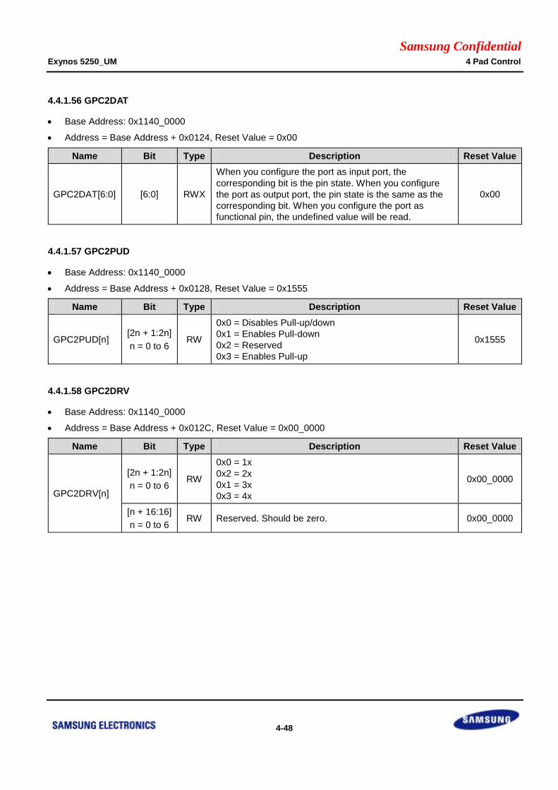
Samsung Confidential Exynos 5250_UM 4 Pad Control
4-48
4.4.1.56 GPC2DAT
Base Address: 0x1140_0000
Address = Base Address + 0x0124, Reset Value = 0x00
Name Bit Type Description Reset Value
GPC2DAT[6:0] [6:0] RWX
When you configure the port as input port, the
corresponding bit is the pin state. When you configure
the port as output port, the pin state is the same as the
corresponding bit. When you configure the port as
functional pin, the undefined value will be read.
0x00
4.4.1.57 GPC2PUD
Base Address: 0x1140_0000
Address = Base Address + 0x0128, Reset Value = 0x1555
Name Bit Type Description Reset Value
GPC2PUD[n] [2n + 1:2n]
n = 0 to 6 RW
0x0 = Disables Pull-up/down
0x1 = Enables Pull-down
0x2 = Reserved
0x3 = Enables Pull-up
0x1555
4.4.1.58 GPC2DRV
Base Address: 0x1140_0000
Address = Base Address + 0x012C, Reset Value = 0x00_0000
Name Bit Type Description Reset Value
GPC2DRV[n]
[2n + 1:2n]
n = 0 to 6 RW
0x0 = 1x
0x2 = 2x
0x1 = 3x
0x3 = 4x
0x00_0000
[n + 16:16]
n = 0 to 6 RW Reserved. Should be zero. 0x00_0000

Samsung Confidential Exynos 5250_UM 4 Pad Control
4-49
4.4.1.59 GPC2CONPDN
Base Address: 0x1140_0000
Address = Base Address + 0x0130, Reset Value = 0x0000
Name Bit Type Description Reset Value
GPC2[n] [2n + 1:2n]
n = 0 to 6 RW
0x0 = Output 0
0x1 = Output 1
0x2 = Input
0x3 = Previous state
0x00
4.4.1.60 GPC2PUDPDN
Base Address: 0x1140_0000
Address = Base Address + 0x0134, Reset Value = 0x0000
Name Bit Type Description Reset Value
GPC2[n] [2n + 1:2n]
n = 0 to 6 RW
0x0 = Disables Pull-up/down
0x1 = Enables Pull-down
0x2 = Reserved
0x3 = Enables Pull-up
0x00

Samsung Confidential Exynos 5250_UM 4 Pad Control
4-50
4.4.1.61 GPC3CON
Base Address: 0x1140_0000
Address = Base Address + 0x0140, Reset Value = 0x0000_0000
Name Bit Type Description Reset Value
GPC3CON[6] [27:24] RW
0x0 = Input
0x1 = Output
0x2 = SD_2_DATA[3]
0x3 to 0xE = Reserved
0xF = EXT_INT11[6]
0x00
GPC3CON[5] [23:20] RW
0x0 = Input
0x1 = Output
0x2 = SD_2_DATA[2]
0x3 to 0xE = Reserved
0xF = EXT_INT11[5]
0x00
GPC3CON[4] [19:16] RW
0x0 = Input
0x1 = Output
0x2 = SD_2_DATA[1]
0x3 to 0xE = Reserved
0xF = EXT_INT11[4]
0x00
GPC3CON[3] [15:12] RW
0x0 = Input
0x1 = Output
0x2 = SD_2_DATA[0]
0x3 to 0xE = Reserved
0xF = EXT_INT11[3]
0x00
GPC3CON[2] [11:8] RW
0x0 = Input
0x1 = Output
0x2 = SD_2_CDn
0x3 = SD_2_nRESET_OUT
0x4 = SD_2_CARD_INT_n
0x5 to 0xE = Reserved
0xF = EXT_INT11[2]
0x00
GPC3CON[1] [7:4] RW
0x0 = Input
0x1 = Output
0x2 = SD_2_CMD
0x3 to 0xE = Reserved
0xF = EXT_INT11[1]
0x00
GPC3CON[0] [3:0] RW
0x0 = Input
0x1 = Output
0x2 = SD_2_CLK
0x3 to 0xE = Reserved
0xF = EXT_INT11[0]
0x00

Samsung Confidential Exynos 5250_UM 4 Pad Control
4-51
4.4.1.62 GPC3DAT
Base Address: 0x1140_0000
Address = Base Address + 0x0144, Reset Value = 0x00
Name Bit Type Description Reset Value
GPC3DAT[6:0] [6:0] RWX
When you configure the port as input port, the
corresponding bit is the pin state. When you configure
the port as output port, the pin state is the same as the
corresponding bit. When you configure the port as
functional pin, the undefined value will be read.
0x00
4.4.1.63 GPC3PUD
Base Address: 0x1140_0000
Address = Base Address + 0x0148, Reset Value = 0x1555
Name Bit Type Description Reset Value
GPC3PUD[n] [2n + 1:2n]
n = 0 to 6 RW
0x0 = Disables Pull-up/down
0x1 = Enables Pull-down
0x2 = Reserved
0x3 = Enables Pull-up
0x1555
4.4.1.64 GPC3DRV
Base Address: 0x1140_0000
Address = Base Address + 0x014C, Reset Value = 0x00_0000
Name Bit Type Description Reset Value
GPC3DRV[n]
[2n + 1:2n]
n = 0 to 6 RW
0x0 = 1x
0x2 = 2x
0x1 = 3x
0x3 = 4x
0x00_0000
[n + 16:16]
n = 0 to 6 RW Reserved. Should be zero. 0x00_0000

Samsung Confidential Exynos 5250_UM 4 Pad Control
4-52
4.4.1.65 GPC3CONPDN
Base Address: 0x1140_0000
Address = Base Address + 0x0150, Reset Value = 0x0000
Name Bit Type Description Reset Value
GPC3[n] [2n + 1:2n]
n = 0 to 6 RW
0x0 = Output 0
0x1 = Output 1
0x2 = Input
0x3 = Previous state
0x00
4.4.1.66 GPC3PUDPDN
Base Address: 0x1140_0000
Address = Base Address + 0x0154, Reset Value = 0x0000
Name Bit Type Description Reset Value
GPC3[n] [2n + 1:2n]
n = 0 to 6 RW
0x0 = Disables Pull-up/down
0x1 = Enables Pull-down
0x2 = Reserved
0x3 = Enables Pull-up
0x00
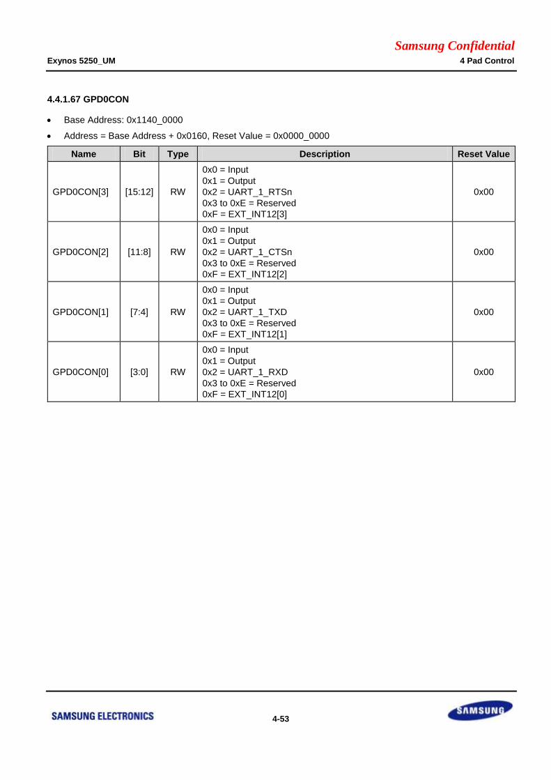
Samsung Confidential Exynos 5250_UM 4 Pad Control
4-53
4.4.1.67 GPD0CON
Base Address: 0x1140_0000
Address = Base Address + 0x0160, Reset Value = 0x0000_0000
Name Bit Type Description Reset Value
GPD0CON[3] [15:12] RW
0x0 = Input
0x1 = Output
0x2 = UART_1_RTSn
0x3 to 0xE = Reserved
0xF = EXT_INT12[3]
0x00
GPD0CON[2] [11:8] RW
0x0 = Input
0x1 = Output
0x2 = UART_1_CTSn
0x3 to 0xE = Reserved
0xF = EXT_INT12[2]
0x00
GPD0CON[1] [7:4] RW
0x0 = Input
0x1 = Output
0x2 = UART_1_TXD
0x3 to 0xE = Reserved
0xF = EXT_INT12[1]
0x00
GPD0CON[0] [3:0] RW
0x0 = Input
0x1 = Output
0x2 = UART_1_RXD
0x3 to 0xE = Reserved
0xF = EXT_INT12[0]
0x00

Samsung Confidential Exynos 5250_UM 4 Pad Control
4-54
4.4.1.68 GPD0DAT
Base Address: 0x1140_0000
Address = Base Address + 0x0164, Reset Value = 0x00
Name Bit Type Description Reset Value
GPD0DAT[3:0] [3:0] RWX
When you configure the port as input port, the
corresponding bit is the pin state. When you configure
the port as output port, the pin state is the same as the
corresponding bit. When you configure the port as
functional pin, the undefined value will be read.
0x00
4.4.1.69 GPD0PUD
Base Address: 0x1140_0000
Address = Base Address + 0x0168, Reset Value = 0X0055
Name Bit Type Description Reset Value
GPD0PUD[n] [2n + 1:2n]
n = 0 to 3 RW
0x0 = Disables Pull-up/down
0x1 = Enables Pull-down
0x2 = Reserved
0x3 = Enables Pull-up
0x0055
4.4.1.70 GPD0DRV
Base Address: 0x1140_0000
Address = Base Address + 0x016C, Reset Value = 0x00_0000
Name Bit Type Description Reset Value
GPD0DRV[n]
[2n + 1:2n]
n = 0 to 3 RW
0x0 = 1x
0x2 = 2x
0x1 = 3x
0x3 = 4x
0x00_0000
[n + 16:16]
n = 0 to 3 RW Reserved. Should be zero. 0x00_0000

Samsung Confidential Exynos 5250_UM 4 Pad Control
4-55
4.4.1.71 GPD0CONPDN
Base Address: 0x1140_0000
Address = Base Address + 0x170, Reset Value = 0x0000
Name Bit Type Description Reset Value
GPD0[n] [2n + 1:2n]
n = 0 to 3 RW
0x0 = Output 0
0x1 = Output 1
0x2 = Input
0x3 = Previous state
0x00
4.4.1.72 GPD0PUDPDN
Base Address: 0x1140_0000
Address = Base Address + 0x0174, Reset Value = 0x0000
Name Bit Type Description Reset Value
GPD0[n] [2n + 1:2n]
n = 0 to 3 RW
0x0 = Disables Pull-up/down
0x1 = Enables Pull-down
0x2 = Reserved
0x3 = Enables Pull-up
0x00

Samsung Confidential Exynos 5250_UM 4 Pad Control
4-56
4.4.1.73 GPD1CON
Base Address: 0x1140_0000
Address = Base Address + 0x0180, Reset Value = 0x0000_0000
Name Bit Type Description Reset Value
GPD1CON[7] [31:28] RW
0x0 = Input
0x1 = Output
0x2 = Reserved
0x3 = Reserved
0x4 = HSI_CAREADY
0x5 to 0xE = Reserved
0xF = EXT_INT13[7]
0x00
GPD1CON[6] [27:24] RW
0x0 = Input
0x1 = Output
0x2 = Reserved
0x3 = Reserved
0x4 = HSI_ACFLAG
0x5 to 0xE = Reserved
0xF = EXT_INT13[6]
0x00
GPD1CON[5] [23:20] RW
0x0 = Input
0x1 = Output
0x2 = Reserved
0x3 = Reserved
0x4 = HSI_ACDATA
0x5 to 0xE = Reserved
0xF = EXT_INT13[5]
0x00
GPD1CON[4] [19:16] RW
0x0 = Input
0x1 = Output
0x2 = Reserved
0x3 = Reserved
0x4 = HSI_ACWAKE
0x5 to 0xE = Reserved
0xF = EXT_INT13[4]
0x00
GPD1CON[3] [15:12] RW
0x0 = Input
0x1 = Output
0x2 = Reserved
0x3 = Reserved
0x4 = HSI_ACREADY
0x5 to 0xE = Reserved
0xF = EXT_INT13[3]
0x00
GPD1CON[2] [11:8] RW
0x0 = Input
0x1 = Output
0x2 = Reserved
0x3 = Reserved
0x4 = HSI_CAFLAG
0x5 to 0xE = Reserved
0xF = EXT_INT13[2]
0x00
GPD1CON[1] [7:4] RW 0x0 = Input
0x1 = Output 0x00
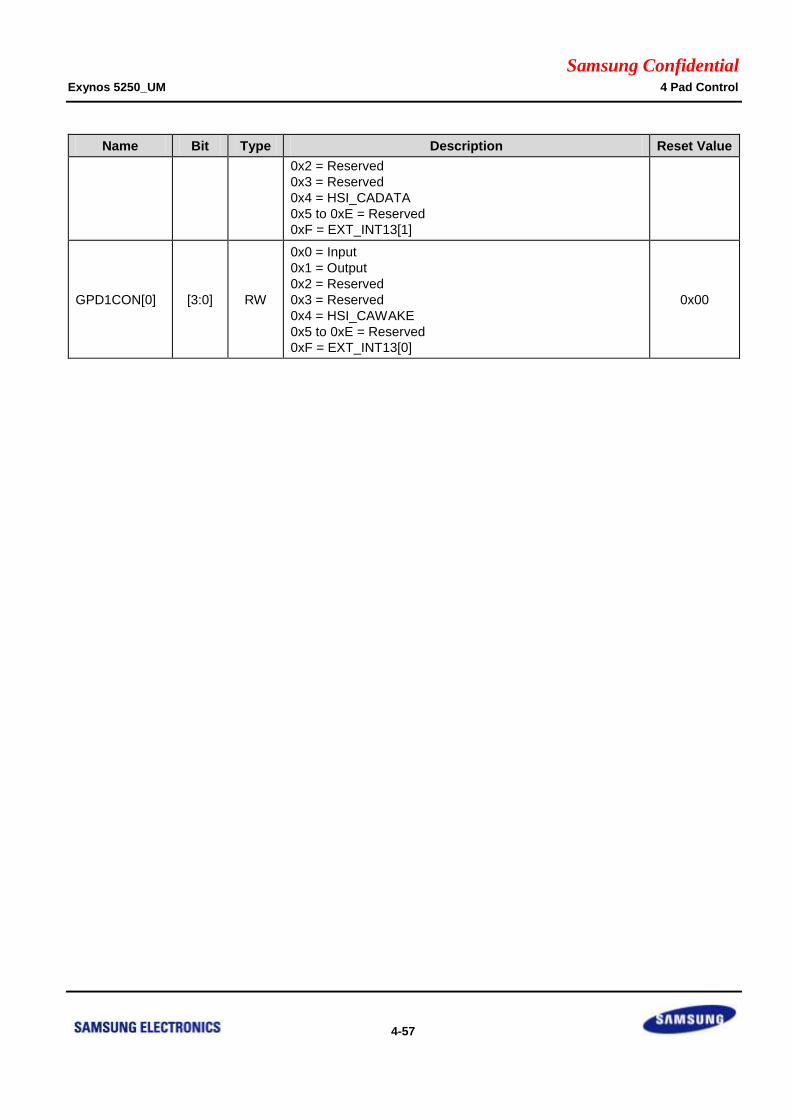
Samsung Confidential Exynos 5250_UM 4 Pad Control
4-57
Name Bit Type Description Reset Value
0x2 = Reserved
0x3 = Reserved
0x4 = HSI_CADATA
0x5 to 0xE = Reserved
0xF = EXT_INT13[1]
GPD1CON[0] [3:0] RW
0x0 = Input
0x1 = Output
0x2 = Reserved
0x3 = Reserved
0x4 = HSI_CAWAKE
0x5 to 0xE = Reserved
0xF = EXT_INT13[0]
0x00

Samsung Confidential Exynos 5250_UM 4 Pad Control
4-58
4.4.1.74 GPD1DAT
Base Address: 0x1140_0000
Address = Base Address + 0x0184, Reset Value = 0x00
Name Bit Type Description Reset Value
GPD1DAT[7:0] [7:0] RWX
When you configure the port as input port, the
corresponding bit is the pin state. When you configure
the port as output port, the pin state is the same as the
corresponding bit. When you configure the port as
functional pin, the undefined value will be read.
0x00
4.4.1.75 GPD1PUD
Base Address: 0x1140_0000
Address = Base Address + 0x0188, Reset Value = 0x5555
Name Bit Type Description Reset Value
GPD1PUD[n] [2n + 1:2n]
n = 0 to 7 RW
0x0 = Disables Pull-up/down
0x1 = Enables Pull-down
0x2 = Reserved
0x3 = Enables Pull-up
0x5555
4.4.1.76 GPD1DRV
Base Address: 0x1140_0000
Address = Base Address + 0x018C, Reset Value = 0x00_0000
Name Bit Type Description Reset Value
GPD1DRV[n]
[2n + 1:2n]
n = 0 to 7 RW
0x0 = 1x
0x2 = 2x
0x1 = 3x
0x3 = 4x
0x00_0000
[n + 16:16]
n = 0 to 7 RW Reserved. Should be zero. 0x00_0000

Samsung Confidential Exynos 5250_UM 4 Pad Control
4-59
4.4.1.77 GPD1CONPDN
Base Address: 0x1140_0000
Address = Base Address + 0x0190, Reset Value = 0x0000
Name Bit Type Description Reset Value
GPD1[n] [2n + 1:2n]
n = 0 to 7 RW
0x0 = Output 0
0x1 = Output 1
0x2 = Input
0x3 = Previous state
0x00
4.4.1.78 GPD1PUDPDN
Base Address: 0x1140_0000
Address = Base Address + 0x0194, Reset Value = 0x0000
Name Bit Type Description Reset Value
GPD1[n] [2n + 1:2n]
n = 0 to 7 RW
0x0 = Disables Pull-up/down
0x1 = Enables Pull-down
0x2 = Reserved
0x3 = Enables Pull-up
0x00
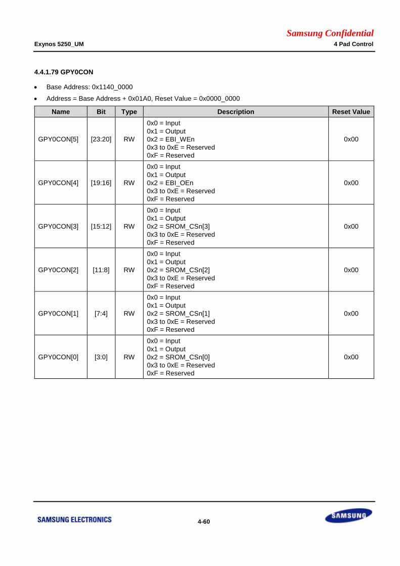
Samsung Confidential Exynos 5250_UM 4 Pad Control
4-60
4.4.1.79 GPY0CON
Base Address: 0x1140_0000
Address = Base Address + 0x01A0, Reset Value = 0x0000_0000
Name Bit Type Description Reset Value
GPY0CON[5] [23:20] RW
0x0 = Input
0x1 = Output
0x2 = EBI_WEn
0x3 to 0xE = Reserved
0xF = Reserved
0x00
GPY0CON[4] [19:16] RW
0x0 = Input
0x1 = Output
0x2 = EBI_OEn
0x3 to 0xE = Reserved
0xF = Reserved
0x00
GPY0CON[3] [15:12] RW
0x0 = Input
0x1 = Output
0x2 = SROM_CSn[3]
0x3 to 0xE = Reserved
0xF = Reserved
0x00
GPY0CON[2] [11:8] RW
0x0 = Input
0x1 = Output
0x2 = SROM_CSn[2]
0x3 to 0xE = Reserved
0xF = Reserved
0x00
GPY0CON[1] [7:4] RW
0x0 = Input
0x1 = Output
0x2 = SROM_CSn[1]
0x3 to 0xE = Reserved
0xF = Reserved
0x00
GPY0CON[0] [3:0] RW
0x0 = Input
0x1 = Output
0x2 = SROM_CSn[0]
0x3 to 0xE = Reserved
0xF = Reserved
0x00

Samsung Confidential Exynos 5250_UM 4 Pad Control
4-61
4.4.1.80 GPY0DAT
Base Address: 0x1140_0000
Address = Base Address + 0x01A4, Reset Value = 0x00
Name Bit Type Description Reset Value
GPY0DAT[5:0] [5:0] RWX
When you configure the port as input port, the
corresponding bit is the pin state. When you configure
the port as output port, the pin state is the same as the
corresponding bit. When you configure the port as
functional pin, the undefined value will be read.
0x00
4.4.1.81 GPY0PUD
Base Address: 0x1140_0000
Address = Base Address + 0x01A8, Reset Value = 0x0FFF
Name Bit Type Description Reset Value
GPY0PUD[n] [2n + 1:2n]
n = 0 to 5 RW
0x0 = Disables Pull-up/down
0x1 = Enables Pull-down
0x2 = Reserved
0x3 = Enables Pull-up
0x0FFF
4.4.1.82 GPY0DRV
Base Address: 0x1140_0000
Address = Base Address + 0x01AC, Reset Value = 0x00_0AAA
Name Bit Type Description Reset Value
GPY0DRV[n]
[2n + 1:2n]
n = 0 to 5 RW
0x0 = 1x
0x2 = 2x
0x1 = 3x
0x3 = 4x
0x00_0AAA
[n + 16:16]
n = 0 to 5 RW Reserved. Should be zero. 0x00_0000

Samsung Confidential Exynos 5250_UM 4 Pad Control
4-62
4.4.1.83 GPY0CONPDN
Base Address: 0x1140_0000
Address = Base Address + 0x01B0, Reset Value = 0x0000
Name Bit Type Description Reset Value
GPY0[n] [2n + 1:2n]
n = 0 to 5 RW
0x0 = Output 0
0x1 = Output 1
0x2 = Input
0x3 = Previous state
0x00
4.4.1.84 GPY0PUDPDN
Base Address: 0x1140_0000
Address = Base Address + 0x01B4, Reset Value = 0x0000
Name Bit Type Description Reset Value
GPY0[n] [2n + 1:2n]
n = 0 to 5 RW
0x0 = Disables Pull-up/down
0x1 = Enables Pull-down
0x2 = Reserved
0x3 = Enables Pull-up
0x00
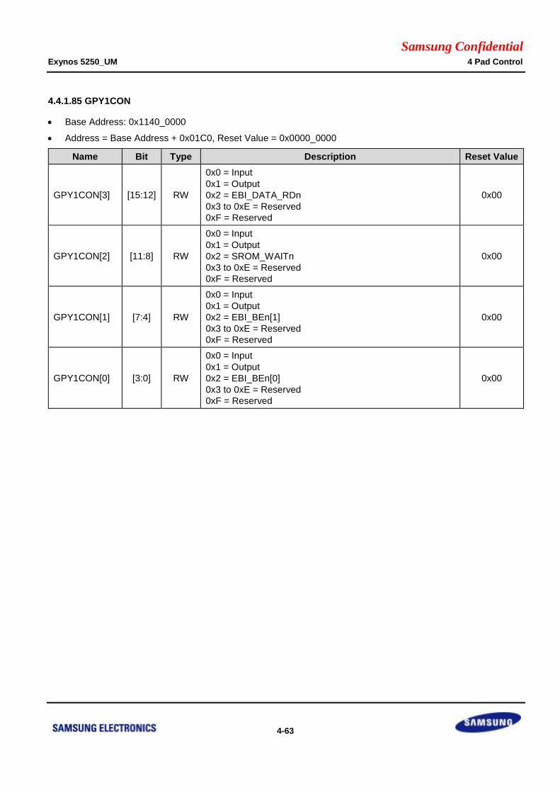
Samsung Confidential Exynos 5250_UM 4 Pad Control
4-63
4.4.1.85 GPY1CON
Base Address: 0x1140_0000
Address = Base Address + 0x01C0, Reset Value = 0x0000_0000
Name Bit Type Description Reset Value
GPY1CON[3] [15:12] RW
0x0 = Input
0x1 = Output
0x2 = EBI_DATA_RDn
0x3 to 0xE = Reserved
0xF = Reserved
0x00
GPY1CON[2] [11:8] RW
0x0 = Input
0x1 = Output
0x2 = SROM_WAITn
0x3 to 0xE = Reserved
0xF = Reserved
0x00
GPY1CON[1] [7:4] RW
0x0 = Input
0x1 = Output
0x2 = EBI_BEn[1]
0x3 to 0xE = Reserved
0xF = Reserved
0x00
GPY1CON[0] [3:0] RW
0x0 = Input
0x1 = Output
0x2 = EBI_BEn[0]
0x3 to 0xE = Reserved
0xF = Reserved
0x00

Samsung Confidential Exynos 5250_UM 4 Pad Control
4-64
4.4.1.86 GPY1DAT
Base Address: 0x1140_0000
Address = Base Address + 0x01C4, Reset Value = 0x00
Name Bit Type Description Reset Value
GPY1DAT[3:0] [3:0] RWX
When you configure the port as input port, the
corresponding bit is the pin state. When you configure
the port as output port, the pin state is the same as the
corresponding bit. When you configure the port as
functional pin, the undefined value will be read.
0x00
4.4.1.87 GPY1PUD
Base Address: 0x1140_0000
Address = Base Address + 0x01C8, Reset Value = 0x00FF
Name Bit Type Description Reset Value
GPY1PUD[n] [2n + 1:2n]
n = 0 to 3 RW
0x0 = Disables Pull-up/down
0x1 = Enables Pull-down
0x2 = Reserved
0x3 = Enables Pull-up
0x00FF
4.4.1.88 GPY1DRV
Base Address: 0x1140_0000
Address = Base Address + 0x01CC, Reset Value = 0x00_00AA
Name Bit Type Description Reset Value
GPY1DRV[n]
[2n + 1:2n]
n = 0 to 3 RW
0x0 = 1x
0x2 = 2x
0x1 = 3x
0x3 = 4x
0x00_00AA
[n + 16:16]
n = 0 to 3 RW Reserved. Should be zero. 0x00_00AA

Samsung Confidential Exynos 5250_UM 4 Pad Control
4-65
4.4.1.89 GPY1CONPDN
Base Address: 0x1140_0000
Address = Base Address + 0x01D0, Reset Value = 0x0000
Name Bit Type Description Reset Value
GPY1[n] [2n + 1:2n]
n = 0 to 3 RW
0x0 = Output 0
0x1 = Output 1
0x2 = Input
0x3 = Previous state
0x00
4.4.1.90 GPY1PUDPDN
Base Address: 0x1140_0000
Address = Base Address + 0x01D4, Reset Value = 0x0000
Name Bit Type Description Reset Value
GPY1[n] [2n + 1:2n]
n = 0 to 3 RW
0x0 = Disables Pull-up/down
0x1 = Enables Pull-down
0x2 = Reserved
0x3 = Enables Pull-up
0x00

Samsung Confidential Exynos 5250_UM 4 Pad Control
4-66
4.4.1.91 GPY2CON
Base Address: 0x1140_0000
Address = Base Address + 0x01E0, Reset Value = 0x0000_0000
Name Bit Type Description Reset Value
GPY2CON[5] [23:20] RW
0x0 = Input
0x1 = Output
0x2 = Reserved
0x3 to 0xE = Reserved
0xF = Reserved
0x00
GPY2CON[4] [19:16] RW
0x0 = Input
0x1 = Output
0x2 to 0xE = Reserved
0xF = Reserved
0x00
GPY2CON[3] [15:12] RW
0x0 = Input
0x1 = Output
0x2 = to 0xE = Reserved
0xF = Reserved
0x00
GPY2CON[2] [11:8] RW
0x0 = Input
0x1 = Output
0x2 to 0xE = Reserved
0xF = Reserved
0x00
GPY2CON[1] [7:4] RW
0x0 = Input
0x1 = Output
0x2 to 0xE = Reserved
0xF = Reserved
0x00
GPY2CON[0] [3:0] RW
0x0 = Input
0x1 = Output
0x2 to 0xE = Reserved
0xF = Reserved
0x00

Samsung Confidential Exynos 5250_UM 4 Pad Control
4-67
4.4.1.92 GPY2DAT
Base Address: 0x1140_0000
Address = Base Address + 0x01E4, Reset Value = 0x00
Name Bit Type Description Reset Value
GPY2DAT[5:0] [5:0] RWX
When you configure the port as input port, the
corresponding bit is the pin state. When you configure
the port as output port, the pin state is the same as the
corresponding bit. When you configure the port as
functional pin, the undefined value will be read.
0x00
4.4.1.93 GPY2PUD
Base Address: 0x1140_0000
Address = Base Address + 0x01E8, Reset Value = 0x0FFF
Name Bit Type Description Reset Value
GPY2PUD[n] [2n + 1:2n]
n = 0 to 5 RW
0x0 = Disables Pull-up/down
0x1 = Enables Pull-down
0x2 = Reserved
0x3 = Enables Pull-up
0x0FFF
4.4.1.94 GPY2DRV
Base Address: 0x1140_0000
Address = Base Address + 0x01EC, Reset Value = 0x00_0AAA
Name Bit Type Description Reset Value
GPY2DRV[n]
[2n + 1:2n]
n = 0 to 5 RW
0x0 = 1x
0x2 = 2x
0x1 = 3x
0x3 = 4x
0x00_0AAA
[n + 16:16]
n = 0 to 5 RW Reserved. Should be zero. 0x00_0000

Samsung Confidential Exynos 5250_UM 4 Pad Control
4-68
4.4.1.95 GPY2CONPDN
Base Address: 0x1140_0000
Address = Base Address + 0x01F0, Reset Value = 0x0000
Name Bit Type Description Reset Value
GPY2[n] [2n + 1:2n]
n = 0 to 5 RW
0x0 = Output 0
0x1 = Output 1
0x2 = Input
0x3 = Previous state
0x00
4.4.1.96 GPY2PUDPDN
Base Address: 0x1140_0000
Address = Base Address + 0x01F4, Reset Value = 0x0000
Name Bit Type Description Reset Value
GPY2[n] [2n + 1:2n]
n = 0 to 5 RW
0x0 = Disables Pull-up/down
0x1 = Enables Pull-down
0x2 = Reserved
0x3 = Enables Pull-up
0x00

Samsung Confidential Exynos 5250_UM 4 Pad Control
4-69
4.4.1.97 GPY3CON
Base Address: 0x1140_0000
Address = Base Address + 0x0200, Reset Value = 0x0000_0000
Name Bit Type Description Reset Value
GPY3CON[7] [31:28] RW
0x0 = Input
0x1 = Output
0x2 = EBI_ADDR[7]
0x3 to 0xE = Reserved
0xF = Reserved
0x00
GPY3CON[6] [27:24] RW
0x0 = Input
0x1 = Output
0x2 = EBI_ADDR[6]
0x3 to 0xE = Reserved
0xF = Reserved
0x00
GPY3CON[5] [23:20] RW
0x0 = Input
0x1 = Output
0x2 = EBI_ADDR[5]
0x3 to 0xE = Reserved
0xF = Reserved
0x00
GPY3CON[4] [19:16] RW
0x0 = Input
0x1 = Output
0x2 = EBI_ADDR[4]
0x3 to 0xE = Reserved
0xF = Reserved
0x00
GPY3CON[3] [15:12] RW
0x0 = Input
0x1 = Output
0x2 = EBI_ADDR[3]
0x3 to 0xE = Reserved
0xF = Reserved
0x00
GPY3CON[2] [11:8] RW
0x0 = Input
0x1 = Output
0x2 = EBI_ADDR[2]
0x3 to 0xE = Reserved
0xF = Reserved
0x00
GPY3CON[1] [7:4] RW
0x0 = Input
0x1 = Output
0x2 = EBI_ADDR[1]
0x3 to 0xE = Reserved
0xF = Reserved
0x00
GPY3CON[0] [3:0] RW
0x0 = Input
0x1 = Output
0x2 = EBI_ADDR[0]
0x3 to 0xE = Reserved
0xF = Reserved
0x00

Samsung Confidential Exynos 5250_UM 4 Pad Control
4-70
4.4.1.98 GPY3DAT
Base Address: 0x1140_0000
Address = Base Address + 0x0204, Reset Value = 0x00
Name Bit Type Description Reset Value
GPY3DAT[7:0] [7:0] RWX
When you configure the port as input port, the
corresponding bit is the pin state. When you configure
the port as output port, the pin state is the same as the
corresponding bit. When you configure the port as
functional pin, the undefined value will be read.
0x00
4.4.1.99 GPY3PUD
Base Address: 0x1140_0000
Address = Base Address + 0x0208, Reset Value = 0x5555
Name Bit Type Description Reset Value
GPY3PUD[n] [2n + 1:2n]
n = 0 to 7 RW
0x0 = Disables Pull-up/down
0x1 = Enables Pull-down
0x2 = Reserved
0x3 = Enables Pull-up
0x5555
4.4.1.100 GPY3DRV
Base Address: 0x1140_0000
Address = Base Address + 0x020C, Reset Value = 0x00_AAAA
Name Bit Type Description Reset Value
GPY3DRV[n]
[2n + 1:2n]
n = 0 to 7 RW
0x0 = 1x
0x2 = 2x
0x1 = 3x
0x3 = 4x
0x00_AAAA
[n + 16:16]
n = 0 to 7 RW Reserved. Should be zero. 0x00_0000

Samsung Confidential Exynos 5250_UM 4 Pad Control
4-71
4.4.1.101 GPY3CONPDN
Base Address: 0x1140_0000
Address = Base Address + 0x0210, Reset Value = 0x0000
Name Bit Type Description Reset Value
GPY3[n] [2n + 1:2n]
n = 0 to 7 RW
0x0 = Output 0
0x1 = Output 1
0x2 = Input
0x3 = Previous state
0x00
4.4.1.102 GPY3PUDPDN
Base Address: 0x1140_0000
Address = Base Address + 0x0214, Reset Value = 0x0000
Name Bit Type Description Reset Value
GPY3[n] [2n + 1:2n]
n = 0 to 7 RW
0x0 = Disables Pull-up/down
0x1 = Enables Pull-down
0x2 = Reserved
0x3 = Enables Pull-up
0x00

Samsung Confidential Exynos 5250_UM 4 Pad Control
4-72
4.4.1.103 GPY4CON
Base Address: 0x1140_0000
Address = Base Address + 0x0220, Reset Value = 0x0000_0000
Name Bit Type Description Reset Value
GPY4CON[7] [31:28] RW
0x0 = Input
0x1 = Output
0x2 = EBI_ADDR[15]
0x3 = HSI_CAREADY
0x4 to 0xE = Reserved
0xF = Reserved
0x00
GPY4CON[6] [27:24] RW
0x0 = Input
0x1 = Output
0x2 = EBI_ADDR[14]
0x3 = HSI_ACFLAG
0x4 to 0xE = Reserved
0xF = Reserved
0x00
GPY4CON[5] [23:20] RW
0x0 = Input
0x1 = Output
0x2 = EBI_ADDR[13]
0x3 = HSI_ACDATA
0x4 to 0xE = Reserved
0xF = Reserved
0x00
GPY4CON[4] [19:16] RW
0x0 = Input
0x1 = Output
0x2 = EBI_ADDR[12]
0x3 = HSI_ACWAKE
0x4 to 0xE = Reserved
0xF = Reserved
0x00
GPY4CON[3] [15:12] RW
0x0 = Input
0x1 = Output
0x2 = EBI_ADDR[11]
0x3 = HSI_ACREADY
0x4 to 0xE = Reserved
0xF = Reserved
0x00
GPY4CON[2] [11:8] RW
0x0 = Input
0x1 = Output
0x2 = EBI_ADDR[10]
0x3 = HSI_CAFLAG
0x4 to 0xE = Reserved
0xF = Reserved
0x00
GPY4CON[1] [7:4] RW
0x0 = Input
0x1 = Output
0x2 = EBI_ADDR[9]
0x3 = HSI_CADATA
0x4 to 0xE = Reserved
0xF = Reserved
0x00
GPY4CON[0] [3:0] RW 0x0 = Input
0x1 = Output 0x00

Samsung Confidential Exynos 5250_UM 4 Pad Control
4-73
Name Bit Type Description Reset Value
0x2 = EBI_ADDR[8]
0x3 = HSI_CAWAKE
0x4 to 0xE = Reserved
0xF = Reserved

Samsung Confidential Exynos 5250_UM 4 Pad Control
4-74
4.4.1.104 GPY4DAT
Base Address: 0x1140_0000
Address = Base Address + 0x0224, Reset Value = 0x00
Name Bit Type Description Reset Value
GPY4DAT[7:0] [7:0] RWX
When you configure the port as input port, the
corresponding bit is the pin state. When you configure
the port as output port, the pin state is the same as the
corresponding bit. When you configure the port as
functional pin, the undefined value will be read.
0x00
4.4.1.105 GPY4PUD
Base Address: 0x1140_0000
Address = Base Address + 0x0228, Reset Value = 0x5555
Name Bit Type Description Reset Value
GPY4PUD[n] [2n + 1:2n]
n = 0 to 7 RW
0x0 = Disables Pull-up/down
0x1 = Enables Pull-down
0x2 = Reserved
0x3 = Enables Pull-up
0x5555
4.4.1.106 GPY4DRV
Base Address: 0x1140_0000
Address = Base Address + 0x022C, Reset Value = 0x00_AAAA
Name Bit Type Description Reset Value
GPY4DRV[n]
[2n + 1:2n]
n = 0 to 7 RW
0x0 = 1x
0x2 = 2x
0x1 = 3x
0x3 = 4x
0x00_AAAA
[n + 16:16]
N = 0 to 7 RW Reserved. Should be zero. 0x00_0000
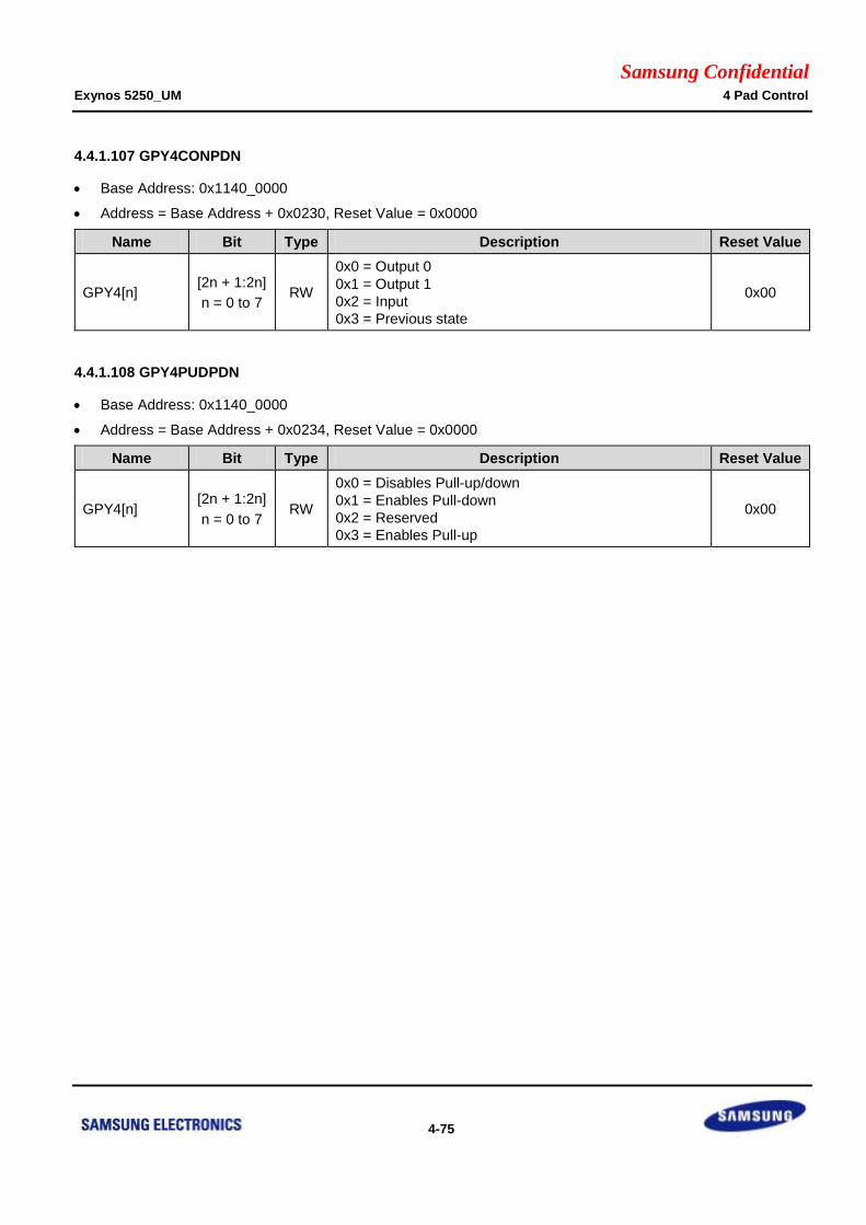
Samsung Confidential Exynos 5250_UM 4 Pad Control
4-75
4.4.1.107 GPY4CONPDN
Base Address: 0x1140_0000
Address = Base Address + 0x0230, Reset Value = 0x0000
Name Bit Type Description Reset Value
GPY4[n] [2n + 1:2n]
n = 0 to 7 RW
0x0 = Output 0
0x1 = Output 1
0x2 = Input
0x3 = Previous state
0x00
4.4.1.108 GPY4PUDPDN
Base Address: 0x1140_0000
Address = Base Address + 0x0234, Reset Value = 0x0000
Name Bit Type Description Reset Value
GPY4[n] [2n + 1:2n]
n = 0 to 7 RW
0x0 = Disables Pull-up/down
0x1 = Enables Pull-down
0x2 = Reserved
0x3 = Enables Pull-up
0x00

Samsung Confidential Exynos 5250_UM 4 Pad Control
4-76
4.4.1.109 GPY5CON
Base Address: 0x1140_0000
Address = Base Address + 0x0240, Reset Value = 0x0000_0000
Name Bit Type Description Reset Value
GPY5CON[7] [31:28] RW
0x0 = Input
0x1 = Output
0x2 = EBI_DATA[7]
0x3 to 0xE = Reserved
0xF = Reserved
0x00
GPY5CON[6] [27:24] RW
0x0 = Input
0x1 = Output
0x2 = EBI_DATA[6]
0x3 to 0xE = Reserved
0xF = Reserved
0x00
GPY5CON[5] [23:20] RW
0x0 = Input
0x1 = Output
0x2 = EBI_DATA[5]
0x3 to 0xE = Reserved
0xF = Reserved
0x00
GPY5CON[4] [19:16] RW
0x0 = Input
0x1 = Output
0x2 = EBI_DATA[4]
0x3 to 0xE = Reserved
0xF = Reserved
0x00
GPY5CON[3] [15:12] RW
0x0 = Input
0x1 = Output
0x2 = EBI_DATA[3]
0x3 to 0xE = Reserved
0xF = Reserved
0x00
GPY5CON[2] [11:8] RW
0x0 = Input
0x1 = Output
0x2 = EBI_DATA[2]
0x3 to 0xE = Reserved
0xF = Reserved
0x00
GPY5CON[1] [7:4] RW
0x0 = Input
0x1 = Output
0x2 = EBI_DATA[1]
0x3 to 0xE = Reserved
0xF = Reserved
0x00
GPY5CON[0] [3:0] RW
0x0 = Input
0x1 = Output
0x2 = EBI_DATA[0]
0x3 to 0xE = Reserved
0xF = Reserved
0x00

Samsung Confidential Exynos 5250_UM 4 Pad Control
4-77
4.4.1.110 GPY5DAT
Base Address: 0x1140_0000
Address = Base Address + 0x0244, Reset Value = 0x00
Name Bit Type Description Reset Value
GPY5DAT[7:0] [7:0] RWX
When you configure the port as input port, the
corresponding bit is the pin state. When you configure
the port as output port, the pin state is the same as the
corresponding bit. When you configure the port as
functional pin, the undefined value will be read.
0x00
4.4.1.111 GPY5PUD
Base Address: 0x1140_0000
Address = Base Address + 0x0248, Reset Value = 0x5555
Name Bit Type Description Reset Value
GPY5PUD[n] [2n + 1:2n]
n = 0 to 7 RW
0x0 = Disables Pull-up/down
0x1 = Enables Pull-down
0x2 = Reserved
0x3 = Enables Pull-up
0x5555
4.4.1.112 GPY5DRV
Base Address: 0x1140_0000
Address = Base Address + 0x024C, Reset Value = 0x00_AAAA
Name Bit Type Description Reset Value
GPY5DRV[n]
[2n + 1:2n]
n = 0 to 7 RW
0x0 = 1x
0x2 = 2x
0x1 = 3x
0x3 = 4x
0x00_AAAA
[n + 16:16]
n = 0 to 7 RW Reserved. Should be zero. 0x00_0000

Samsung Confidential Exynos 5250_UM 4 Pad Control
4-78
4.4.1.113 GPY5CONPDN
Base Address: 0x1140_0000
Address = Base Address + 0x0250, Reset Value = 0x0000
Name Bit Type Description Reset Value
GPY5[n] [2n + 1:2n]
n = 0 to 7 RW
0x0 = Output 0
0x1 = Output 1
0x2 = Input
0x3 = Previous state
0x00
4.4.1.114 GPY5PUDPDN
Base Address: 0x1140_0000
Address = Base Address + 0x0254, Reset Value = 0x0000
Name Bit Type Description Reset Value
GPY5[n] [2n + 1:2n]
n = 0 to 7 RW
0x0 = Disables Pull-up/down
0x1 = Enables Pull-down
0x2 = Reserved
0x3 = Enables Pull-up
0x00
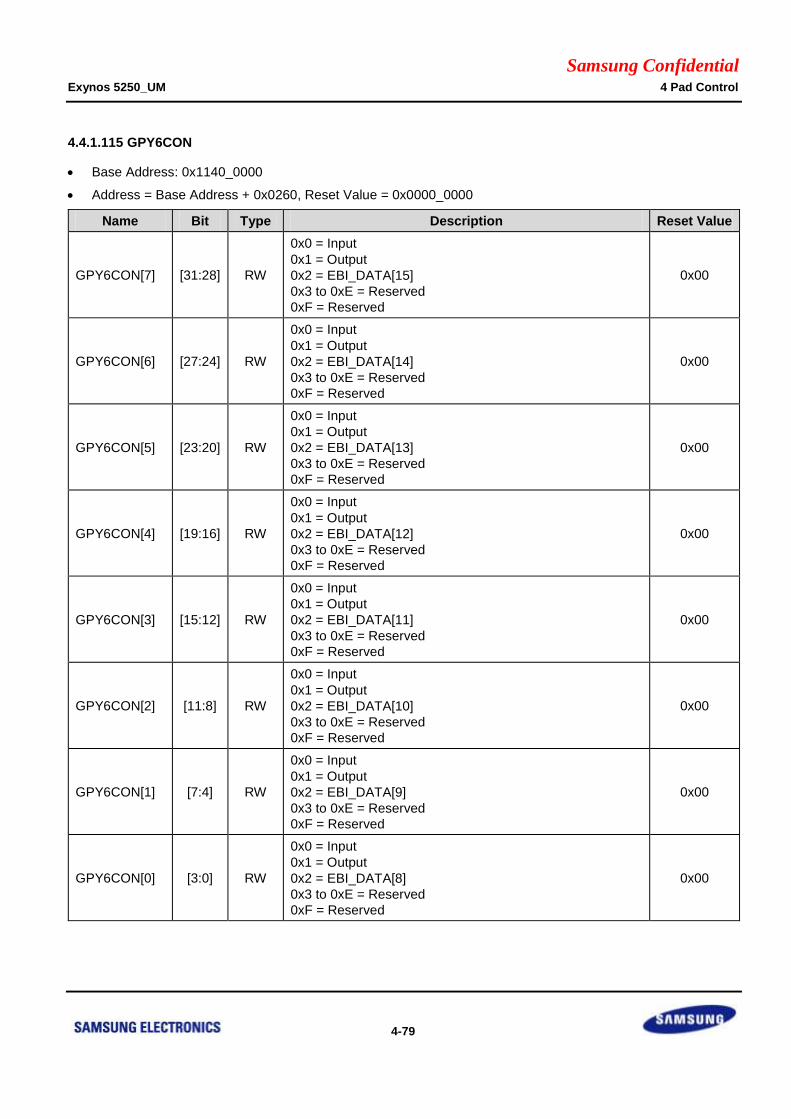
Samsung Confidential Exynos 5250_UM 4 Pad Control
4-79
4.4.1.115 GPY6CON
Base Address: 0x1140_0000
Address = Base Address + 0x0260, Reset Value = 0x0000_0000
Name Bit Type Description Reset Value
GPY6CON[7] [31:28] RW
0x0 = Input
0x1 = Output
0x2 = EBI_DATA[15]
0x3 to 0xE = Reserved
0xF = Reserved
0x00
GPY6CON[6] [27:24] RW
0x0 = Input
0x1 = Output
0x2 = EBI_DATA[14]
0x3 to 0xE = Reserved
0xF = Reserved
0x00
GPY6CON[5] [23:20] RW
0x0 = Input
0x1 = Output
0x2 = EBI_DATA[13]
0x3 to 0xE = Reserved
0xF = Reserved
0x00
GPY6CON[4] [19:16] RW
0x0 = Input
0x1 = Output
0x2 = EBI_DATA[12]
0x3 to 0xE = Reserved
0xF = Reserved
0x00
GPY6CON[3] [15:12] RW
0x0 = Input
0x1 = Output
0x2 = EBI_DATA[11]
0x3 to 0xE = Reserved
0xF = Reserved
0x00
GPY6CON[2] [11:8] RW
0x0 = Input
0x1 = Output
0x2 = EBI_DATA[10]
0x3 to 0xE = Reserved
0xF = Reserved
0x00
GPY6CON[1] [7:4] RW
0x0 = Input
0x1 = Output
0x2 = EBI_DATA[9]
0x3 to 0xE = Reserved
0xF = Reserved
0x00
GPY6CON[0] [3:0] RW
0x0 = Input
0x1 = Output
0x2 = EBI_DATA[8]
0x3 to 0xE = Reserved
0xF = Reserved
0x00

Samsung Confidential Exynos 5250_UM 4 Pad Control
4-80
4.4.1.116 GPY6DAT
Base Address: 0x1140_0000
Address = Base Address + 0x0264, Reset Value = 0x00
Name Bit Type Description Reset Value
GPY6DAT[7:0] [7:0] RWX
When you configure the port as input port, the
corresponding bit is the pin state. When you configure
the port as output port, the pin state is the same as the
corresponding bit. When you configure the port as
functional pin, the undefined value will be read.
0x00
4.4.1.117 GPY6PUD
Base Address: 0x1140_0000
Address = Base Address + 0x0268, Reset Value = 0x5555
Name Bit Type Description Reset Value
GPY6PUD[n] [2n + 1:2n]
n = 0 to 7 RW
0x0 = Disables Pull-up/down
0x1 = Enables Pull-down
0x2 = Reserved
0x3 = Enables Pull-up
0x5555
4.4.1.118 GPY6DRV
Base Address: 0x1140_0000
Address = Base Address + 0x026C, Reset Value = 0x00_AAAA
Name Bit Type Description Reset Value
GPY6DRV[n]
[2n + 1:2n]
n = 0 to 7 RW
0x0 = 1x
0x2 = 2x
0x1 = 3x
0x3 = 4x
0x00_AAAA
[n + 16:16]
N = 0 to 7 RW Reserved. Should be zero. 0x00_0000
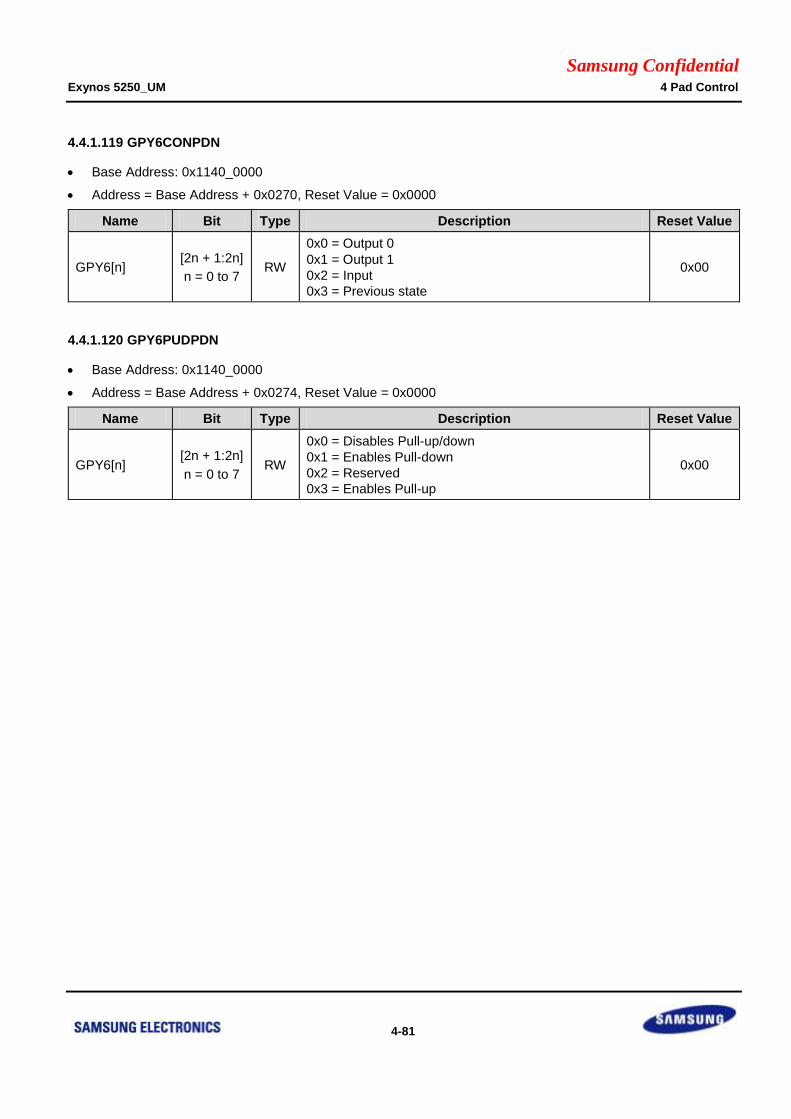
Samsung Confidential Exynos 5250_UM 4 Pad Control
4-81
4.4.1.119 GPY6CONPDN
Base Address: 0x1140_0000
Address = Base Address + 0x0270, Reset Value = 0x0000
Name Bit Type Description Reset Value
GPY6[n] [2n + 1:2n]
n = 0 to 7 RW
0x0 = Output 0
0x1 = Output 1
0x2 = Input
0x3 = Previous state
0x00
4.4.1.120 GPY6PUDPDN
Base Address: 0x1140_0000
Address = Base Address + 0x0274, Reset Value = 0x0000
Name Bit Type Description Reset Value
GPY6[n] [2n + 1:2n]
n = 0 to 7 RW
0x0 = Disables Pull-up/down
0x1 = Enables Pull-down
0x2 = Reserved
0x3 = Enables Pull-up
0x00

Samsung Confidential Exynos 5250_UM 4 Pad Control
4-82
4.4.1.121 ETC0PUD
Base Address: 0x1140_0000
Address = Base Address + 0x0288, Reset Value = 0x04DD
Name Bit Type Description Reset Value
ETC0PUD[n] [2n + 1:2n]
n = 0 to 5 RW
0x0 = Disables Pull-up/down
0x1 = Enables Pull-down
0x2 = Reserved
0x3 = Enables Pull-up
0x04DD
ETC0PUD[1:0] controls XjTRSTn.
ETC0PUD[3:2] controls XjTMS.
ETC0PUD[5:4] controls XjTCK.
ETC0PUD[7:6] controls XjTDI.
ETC0PUD[9:8] controls XjTDO.
ETC0PUD[11:10] controls XjDBGSEL.
4.4.1.122 ETC0DRV
Base Address: 0x1140_0000
Address = Base Address + 0x028C, Reset Value = 0x00_0000
Name Bit Type Description Reset Value
ETC0DRV[n]
[2n + 1:2n]
n = 0 to 5 RW
0x0 = 1x
0x2 = 2x
0x1 = 3x
0x3 = 4x
0x00_0000
[n + 16:16]
n = 0 to 5 RW Reserved. Should be zero. 0x00_0000
ETC0DRV[1:0] controls XjTRSTn.
ETC0DRV[3:2] controls XjTMS.
ETC0DRV[5:4] controls XjTCK.
ETC0DRV[7:6] controls XjTDI.
ETC0DRV[9:8] controls XjTDO.
ETC0DRV[11:10] controls XjDBGSEL.
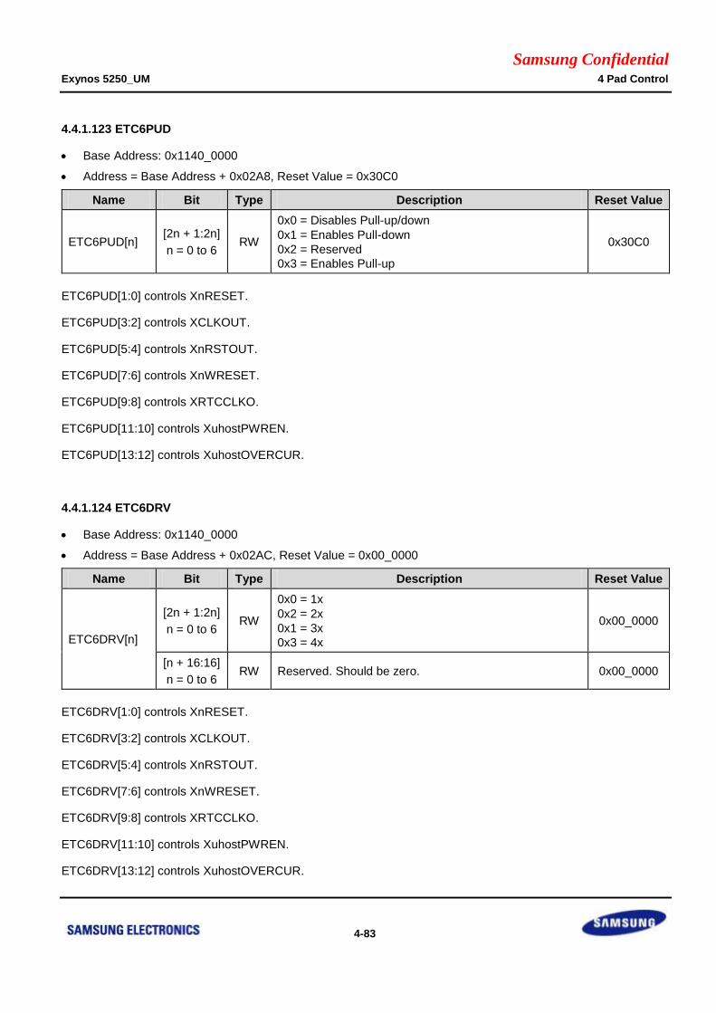
Samsung Confidential Exynos 5250_UM 4 Pad Control
4-83
4.4.1.123 ETC6PUD
Base Address: 0x1140_0000
Address = Base Address + 0x02A8, Reset Value = 0x30C0
Name Bit Type Description Reset Value
ETC6PUD[n] [2n + 1:2n]
n = 0 to 6 RW
0x0 = Disables Pull-up/down
0x1 = Enables Pull-down
0x2 = Reserved
0x3 = Enables Pull-up
0x30C0
ETC6PUD[1:0] controls XnRESET.
ETC6PUD[3:2] controls XCLKOUT.
ETC6PUD[5:4] controls XnRSTOUT.
ETC6PUD[7:6] controls XnWRESET.
ETC6PUD[9:8] controls XRTCCLKO.
ETC6PUD[11:10] controls XuhostPWREN.
ETC6PUD[13:12] controls XuhostOVERCUR.
4.4.1.124 ETC6DRV
Base Address: 0x1140_0000
Address = Base Address + 0x02AC, Reset Value = 0x00_0000
Name Bit Type Description Reset Value
ETC6DRV[n]
[2n + 1:2n]
n = 0 to 6 RW
0x0 = 1x
0x2 = 2x
0x1 = 3x
0x3 = 4x
0x00_0000
[n + 16:16]
n = 0 to 6 RW Reserved. Should be zero. 0x00_0000
ETC6DRV[1:0] controls XnRESET.
ETC6DRV[3:2] controls XCLKOUT.
ETC6DRV[5:4] controls XnRSTOUT.
ETC6DRV[7:6] controls XnWRESET.
ETC6DRV[9:8] controls XRTCCLKO.
ETC6DRV[11:10] controls XuhostPWREN.
ETC6DRV[13:12] controls XuhostOVERCUR.
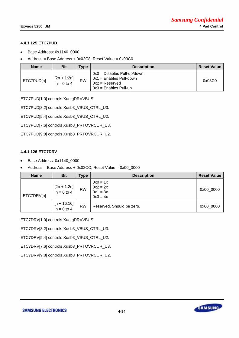
Samsung Confidential Exynos 5250_UM 4 Pad Control
4-84
4.4.1.125 ETC7PUD
Base Address: 0x1140_0000
Address = Base Address + 0x02C8, Reset Value = 0x03C0
Name Bit Type Description Reset Value
ETC7PUD[n] [2n + 1:2n]
n = 0 to 4 RW
0x0 = Disables Pull-up/down
0x1 = Enables Pull-down
0x2 = Reserved
0x3 = Enables Pull-up
0x03C0
ETC7PUD[1:0] controls XuotgDRVVBUS.
ETC7PUD[3:2] controls Xusb3_VBUS_CTRL_U3.
ETC7PUD[5:4] controls Xusb3_VBUS_CTRL_U2.
ETC7PUD[7:6] controls Xusb3_PRTOVRCUR_U3.
ETC7PUD[9:8] controls Xusb3_PRTOVRCUR_U2.
4.4.1.126 ETC7DRV
Base Address: 0x1140_0000
Address = Base Address + 0x02CC, Reset Value = 0x00_0000
Name Bit Type Description Reset Value
ETC7DRV[n]
[2n + 1:2n]
n = 0 to 4 RW
0x0 = 1x
0x2 = 2x
0x1 = 3x
0x3 = 4x
0x00_0000
[n + 16:16]
n = 0 to 4 RW Reserved. Should be zero. 0x00_0000
ETC7DRV[1:0] controls XuotgDRVVBUS.
ETC7DRV[3:2] controls Xusb3_VBUS_CTRL_U3.
ETC7DRV[5:4] controls Xusb3_VBUS_CTRL_U2.
ETC7DRV[7:6] controls Xusb3_PRTOVRCUR_U3.
ETC7DRV[9:8] controls Xusb3_PRTOVRCUR_U2.
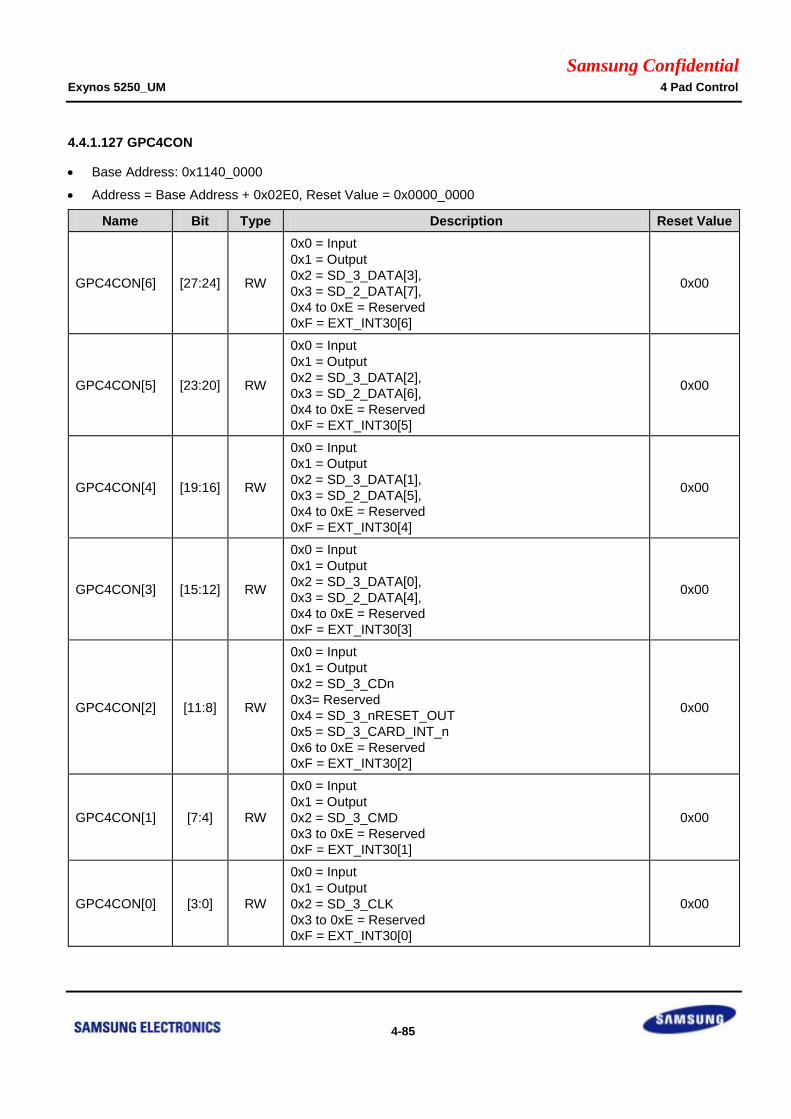
Samsung Confidential Exynos 5250_UM 4 Pad Control
4-85
4.4.1.127 GPC4CON
Base Address: 0x1140_0000
Address = Base Address + 0x02E0, Reset Value = 0x0000_0000
Name Bit Type Description Reset Value
GPC4CON[6] [27:24] RW
0x0 = Input
0x1 = Output
0x2 = SD_3_DATA[3],
0x3 = SD_2_DATA[7],
0x4 to 0xE = Reserved
0xF = EXT_INT30[6]
0x00
GPC4CON[5] [23:20] RW
0x0 = Input
0x1 = Output
0x2 = SD_3_DATA[2],
0x3 = SD_2_DATA[6],
0x4 to 0xE = Reserved
0xF = EXT_INT30[5]
0x00
GPC4CON[4] [19:16] RW
0x0 = Input
0x1 = Output
0x2 = SD_3_DATA[1],
0x3 = SD_2_DATA[5],
0x4 to 0xE = Reserved
0xF = EXT_INT30[4]
0x00
GPC4CON[3] [15:12] RW
0x0 = Input
0x1 = Output
0x2 = SD_3_DATA[0],
0x3 = SD_2_DATA[4],
0x4 to 0xE = Reserved
0xF = EXT_INT30[3]
0x00
GPC4CON[2] [11:8] RW
0x0 = Input
0x1 = Output
0x2 = SD_3_CDn
0x3= Reserved
0x4 = SD_3_nRESET_OUT
0x5 = SD_3_CARD_INT_n
0x6 to 0xE = Reserved
0xF = EXT_INT30[2]
0x00
GPC4CON[1] [7:4] RW
0x0 = Input
0x1 = Output
0x2 = SD_3_CMD
0x3 to 0xE = Reserved
0xF = EXT_INT30[1]
0x00
GPC4CON[0] [3:0] RW
0x0 = Input
0x1 = Output
0x2 = SD_3_CLK
0x3 to 0xE = Reserved
0xF = EXT_INT30[0]
0x00

Samsung Confidential Exynos 5250_UM 4 Pad Control
4-86
4.4.1.128 GPC4DAT
Base Address: 0x1140_0000
Address = Base Address + 0x02E4, Reset Value = 0x00
Name Bit Type Description Reset Value
GPC4DAT[6:0] [6:0] RWX
When the port is configured as input port, the
corresponding bit is the pin state. When the port is
configured as output port, the pin state is the same as
the corresponding bit. When the port is configured as
functional pin, the undefined value will be read.
0x00
4.4.1.129 GPC4PUD
Base Address: 0x1140_0000
Address = Base Address + 0x02E8, Reset Value = 0x1555
Name Bit Type Description Reset Value
GPC4PUD[n] [2n + 1:2n]
n = 0 to 6 RW
0x0 = Disables Pull-up/down
0x1 = Enables Pull-down
0x2 = Reserved
0x3 = Enables Pull-up
0x1555
4.4.1.130 GPC4DRV
Base Address: 0x1140_0000
Address = Base Address + 0x02EC, Reset Value = 0x00_0000
Name Bit Type Description Reset Value
GPC4DRV[n]
[2n + 1:2n]
n = 0 to 6 RW
0x0 = 1x
0x2 = 2x
0x1 = 3x
0x3 = 4x
0x00_0000
[n + 16:16]
n = 0 to 6 RW Reserved. Should be zero. 0x00_0000

Samsung Confidential Exynos 5250_UM 4 Pad Control
4-87
4.4.1.131 GPC4CONPDN
Base Address: 0x1140_0000
Address = Base Address + 0x02F0, Reset Value = 0x0000
Name Bit Type Description Reset Value
GPC4[n] [2n + 1:2n]
n = 0 to 6 RW
0x0 = Output 0
0x1 = Output 1
0x2 = Input
0x3 = Previous state
0x00
4.4.1.132 GPC4PUDPDN
Base Address: 0x1140_0000
Address = Base Address + 0x02F4, Reset Value = 0x0000
Name Bit Type Description Reset Value
GPC4[n] [2n + 1:2n]
n = 0 to 6 RW
0x0 = Disables Pull-up/down
0x1 = Enables Pull-down
0x2 = Reserved
0x3 = Enables Pull-up
0x00

Samsung Confidential Exynos 5250_UM 4 Pad Control
4-88
4.4.1.133 EXT_INT1CON
Base Address: 0x1140_0000
Address = Base Address + 0x0700, Reset Value = 0x0000_0000
Name Bit Type Description Reset Value
RSVD [31] – Reserved 0x0
EXT_INT1
_CON[7] [30:28] RW
Sets the signaling method of EXT_INT1[7]
0x0 = Sets Low level
0x1 = Sets High level
0x2 = Triggers Falling edge
0x3 = Triggers Rising edge
0x4 = Triggers Both edge
0x5 to 0x7 = Reserved
0x0
RSVD [27] – Reserved 0x0
EXT_INT1
_CON[6] [26:24] RW
Setting the signaling method of EXT_INT1[6]
0x0 = Sets Low level
0x1 = Sets High level
0x2 = Triggers Falling edge
0x3 = Triggers Rising edge
0x4 = Triggers Both edge
0x5 to 0x7 = Reserved
0x0
RSVD [23] – Reserved 0x0
EXT_INT1_CO
N[5] [22:20] RW
Setting the signaling method of EXT_INT1[5]
0x0 = Sets Low level
0x1 = Sets High level
0x2 = Triggers Falling edge
0x3 = Triggers Rising edge
0x4 = Triggers Both edge
0x5 to 0x7 = Reserved
0x0
RSVD [19] – Reserved 0x0
EXT_INT1
_CON[4] [18:16] RW
Setting the signaling method of EXT_INT1[4]
0x0 = Sets Low level
0x1 = Sets High level
0x2 = Triggers Falling edge
0x3 = Triggers Rising edge
0x4 = Triggers Both edge
0x5 to 0x7 = Reserved
0x0
RSVD [15] – Reserved 0x0
EXT_INT1
_CON[3] [14:12] RW
Setting the signaling method of EXT_INT1[3]
0x0 = Sets Low level
0x1 = Sets High level
0x2 = Triggers Falling edge
0x3 = Triggers Rising edge
0x4 = Triggers Both edge
0x5 to 0x7 = Reserved
0x0
RSVD [11] – Reserved 0x0
EXT_INT1 [10:8] RW Setting the signaling method of EXT_INT1[2] 0x0

Samsung Confidential Exynos 5250_UM 4 Pad Control
4-89
Name Bit Type Description Reset Value
_CON[2] 0x0 = Sets Low level
0x1 = Sets High level
0x2 = Triggers Falling edge
0x3 = Triggers Rising edge
0x4 = Triggers Both edge
0x5 to 0x7 = Reserved
RSVD [7] – Reserved 0x0
EXT_INT1
_CON[1] [6:4] RW
Setting the signaling method of EXT_INT1[1]
0x0 = Sets Low level
0x1 = Sets High level
0x2 = Triggers Falling edge
0x3 = Triggers Rising edge
0x4 = Triggers Both edge
0x5 to 0x7 = Reserved
0x0
RSVD [3] – Reserved 0x0
EXT_INT1
_CON[0] [2:0] RW
Setting the signaling method of EXT_INT1[0]
0x0 = Sets Low level
0x1 = Sets High level
0x2 = Triggers Falling edge
0x3 = Triggers Rising edge
0x4 = Triggers Both edge
0x5 to 0x7 = Reserved
0x0

Samsung Confidential Exynos 5250_UM 4 Pad Control
4-90
4.4.1.134 EXT_INT2CON
Base Address: 0x1140_0000
Address = Base Address + 0x0704, Reset Value = 0x0000_0000
Name Bit Type Description Reset Value
RSVD [31:24] – Reserved 0x00
RSVD [23] – Reserved 0x0
EXT_INT2
_CON[5] [22:20] RW
Setting the signaling method of EXT_INT2[5]
0x0 = Sets Low level
0x1 = Sets High level
0x2 = Triggers Falling edge
0x3 = Triggers Rising edge
0x4 = Triggers Both edge
0x5 to 0x7 = Reserved
0x0
RSVD [19] – Reserved 0x0
EXT_INT2
_CON[4] [18:16] RW
Setting the signaling method of EXT_INT2[4]
0x0 = Sets Low level
0x1 = Sets High level
0x2 = Triggers Falling edge
0x3 = Triggers Rising edge
0x4 = Triggers Both edge
0x5 to 0x7 = Reserved
0x0
RSVD [15] – Reserved 0x0
EXT_INT2
_CON[3] [14:12] RW
Setting the signaling method of EXT_INT2[3]
0x0 = Sets Low level
0x1 = Sets High level
0x2 = Triggers Falling edge
0x3 = Triggers Rising edge
0x4 = Triggers Both edge
0x5 to 0x7 = Reserved
0x0
RSVD [11] – Reserved 0x0
EXT_INT2
_CON[2] [10:8] RW
Setting the signaling method of EXT_INT2[2]
0x0 = Sets Low level
0x1 = Sets High level
0x2 = Triggers Falling edge
0x3 = Triggers Rising edge
0x4 = Triggers Both edge
0x5 to 0x7 = Reserved
0x0
RSVD [7] – Reserved 0x0
EXT_INT2
_CON[1] [6:4] RW
Setting the signaling method of EXT_INT2[1]
0x0 = Sets Low level
0x1 = Sets High level
0x2 = Triggers Falling edge
0x3 = Triggers Rising edge
0x4 = Triggers Both edge
0x5 to 0x7 = Reserved
0x0
RSVD [3] – Reserved 0x0
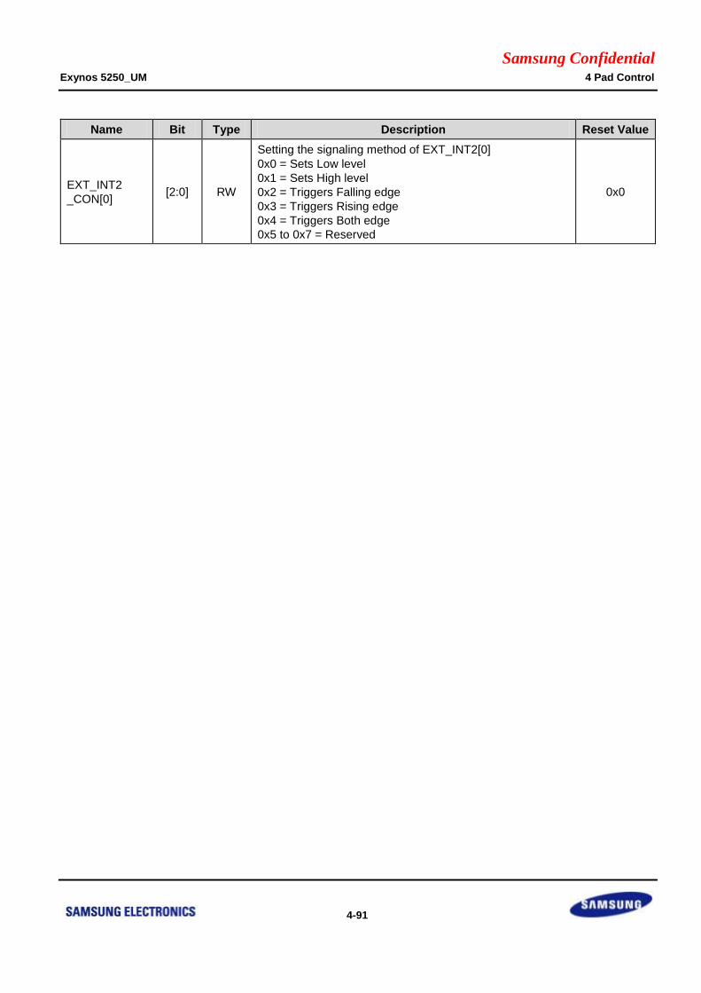
Samsung Confidential Exynos 5250_UM 4 Pad Control
4-91
Name Bit Type Description Reset Value
EXT_INT2
_CON[0] [2:0] RW
Setting the signaling method of EXT_INT2[0]
0x0 = Sets Low level
0x1 = Sets High level
0x2 = Triggers Falling edge
0x3 = Triggers Rising edge
0x4 = Triggers Both edge
0x5 to 0x7 = Reserved
0x0
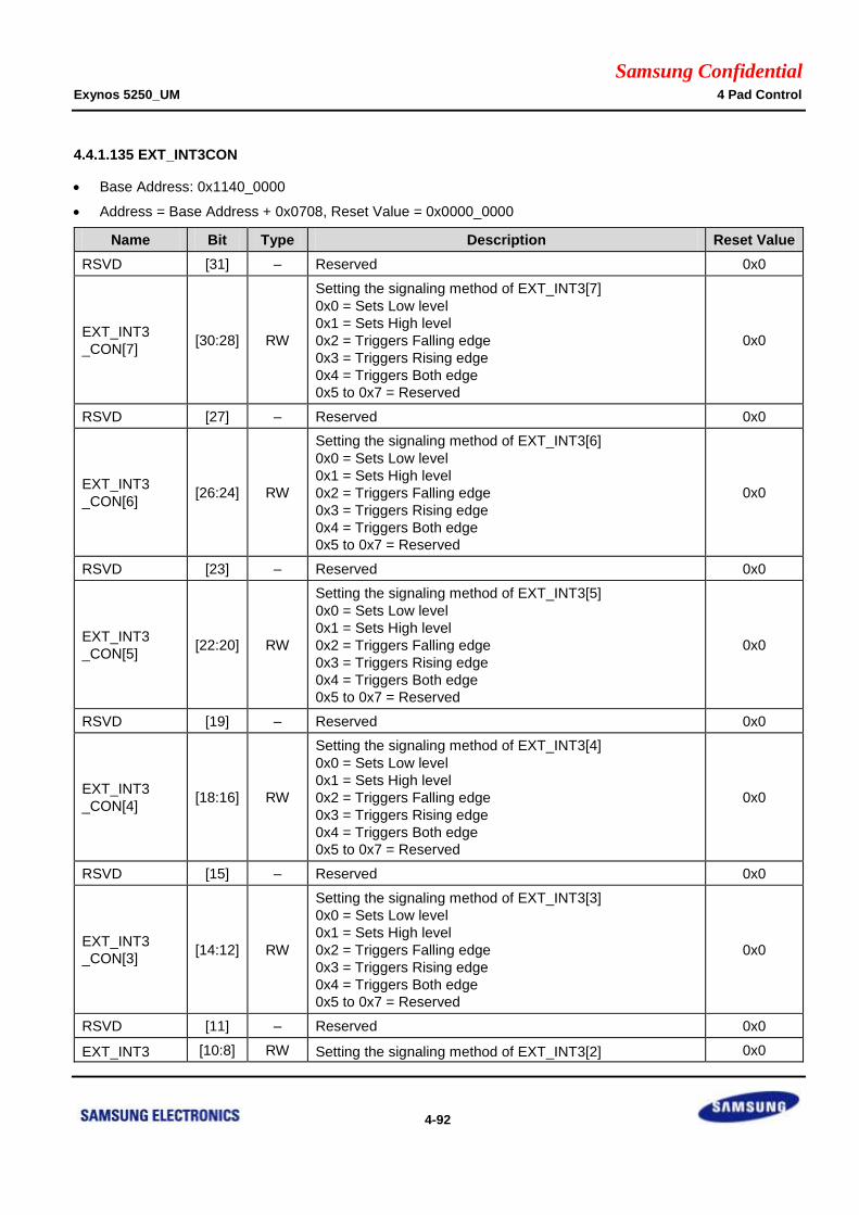
Samsung Confidential Exynos 5250_UM 4 Pad Control
4-92
4.4.1.135 EXT_INT3CON
Base Address: 0x1140_0000
Address = Base Address + 0x0708, Reset Value = 0x0000_0000
Name Bit Type Description Reset Value
RSVD [31] – Reserved 0x0
EXT_INT3
_CON[7] [30:28] RW
Setting the signaling method of EXT_INT3[7]
0x0 = Sets Low level
0x1 = Sets High level
0x2 = Triggers Falling edge
0x3 = Triggers Rising edge
0x4 = Triggers Both edge
0x5 to 0x7 = Reserved
0x0
RSVD [27] – Reserved 0x0
EXT_INT3
_CON[6] [26:24] RW
Setting the signaling method of EXT_INT3[6]
0x0 = Sets Low level
0x1 = Sets High level
0x2 = Triggers Falling edge
0x3 = Triggers Rising edge
0x4 = Triggers Both edge
0x5 to 0x7 = Reserved
0x0
RSVD [23] – Reserved 0x0
EXT_INT3
_CON[5] [22:20] RW
Setting the signaling method of EXT_INT3[5]
0x0 = Sets Low level
0x1 = Sets High level
0x2 = Triggers Falling edge
0x3 = Triggers Rising edge
0x4 = Triggers Both edge
0x5 to 0x7 = Reserved
0x0
RSVD [19] – Reserved 0x0
EXT_INT3
_CON[4] [18:16] RW
Setting the signaling method of EXT_INT3[4]
0x0 = Sets Low level
0x1 = Sets High level
0x2 = Triggers Falling edge
0x3 = Triggers Rising edge
0x4 = Triggers Both edge
0x5 to 0x7 = Reserved
0x0
RSVD [15] – Reserved 0x0
EXT_INT3
_CON[3] [14:12] RW
Setting the signaling method of EXT_INT3[3]
0x0 = Sets Low level
0x1 = Sets High level
0x2 = Triggers Falling edge
0x3 = Triggers Rising edge
0x4 = Triggers Both edge
0x5 to 0x7 = Reserved
0x0
RSVD [11] – Reserved 0x0
EXT_INT3 [10:8] RW Setting the signaling method of EXT_INT3[2] 0x0

Samsung Confidential Exynos 5250_UM 4 Pad Control
4-93
Name Bit Type Description Reset Value
_CON[2] 0x0 = Sets Low level
0x1 = Sets High level
0x2 = Triggers Falling edge
0x3 = Triggers Rising edge
0x4 = Triggers Both edge
0x5 to 0x7 = Reserved
RSVD [7] – Reserved 0x0
EXT_INT3
_CON[1] [6:4] RW
Setting the signaling method of EXT_INT3[1]
0x0 = Sets Low level
0x1 = Sets High level
0x2 = Triggers Falling edge
0x3 = Triggers Rising edge
0x4 = Triggers Both edge
0x5 to 0x7 = Reserved
0x0
RSVD [3] – Reserved 0x0
EXT_INT3
_CON[0] [2:0] RW
Setting the signaling method of EXT_INT3[0]
0x0 = Sets Low level
0x1 = Sets High level
0x2 = Triggers Falling edge
0x3 = Triggers Rising edge
0x4 = Triggers Both edge
0x5 to 0x7 = Reserved
0x0
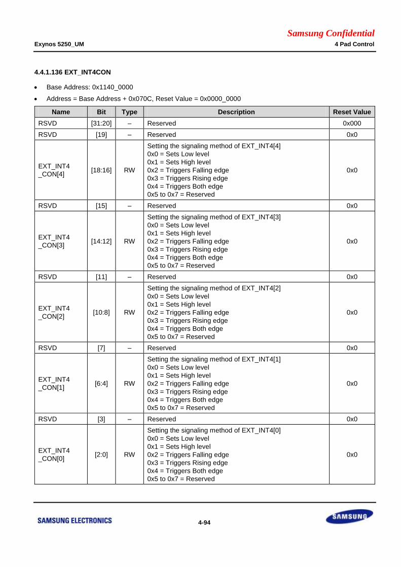
Samsung Confidential Exynos 5250_UM 4 Pad Control
4-94
4.4.1.136 EXT_INT4CON
Base Address: 0x1140_0000
Address = Base Address + 0x070C, Reset Value = 0x0000_0000
Name Bit Type Description Reset Value
RSVD [31:20] – Reserved 0x000
RSVD [19] – Reserved 0x0
EXT_INT4
_CON[4] [18:16] RW
Setting the signaling method of EXT_INT4[4]
0x0 = Sets Low level
0x1 = Sets High level
0x2 = Triggers Falling edge
0x3 = Triggers Rising edge
0x4 = Triggers Both edge
0x5 to 0x7 = Reserved
0x0
RSVD [15] – Reserved 0x0
EXT_INT4
_CON[3] [14:12] RW
Setting the signaling method of EXT_INT4[3]
0x0 = Sets Low level
0x1 = Sets High level
0x2 = Triggers Falling edge
0x3 = Triggers Rising edge
0x4 = Triggers Both edge
0x5 to 0x7 = Reserved
0x0
RSVD [11] – Reserved 0x0
EXT_INT4
_CON[2] [10:8] RW
Setting the signaling method of EXT_INT4[2]
0x0 = Sets Low level
0x1 = Sets High level
0x2 = Triggers Falling edge
0x3 = Triggers Rising edge
0x4 = Triggers Both edge
0x5 to 0x7 = Reserved
0x0
RSVD [7] – Reserved 0x0
EXT_INT4
_CON[1] [6:4] RW
Setting the signaling method of EXT_INT4[1]
0x0 = Sets Low level
0x1 = Sets High level
0x2 = Triggers Falling edge
0x3 = Triggers Rising edge
0x4 = Triggers Both edge
0x5 to 0x7 = Reserved
0x0
RSVD [3] – Reserved 0x0
EXT_INT4
_CON[0] [2:0] RW
Setting the signaling method of EXT_INT4[0]
0x0 = Sets Low level
0x1 = Sets High level
0x2 = Triggers Falling edge
0x3 = Triggers Rising edge
0x4 = Triggers Both edge
0x5 to 0x7 = Reserved
0x0

Samsung Confidential Exynos 5250_UM 4 Pad Control
4-95
4.4.1.137 EXT_INT5CON
Base Address: 0x1140_0000
Address = Base Address + 0x0710, Reset Value = 0x0000_0000
Name Bit Type Description Reset Value
RSVD [31:20] – Reserved 0x000
RSVD [19] – Reserved 0x0
EXT_INT5
_CON[4] [18:16] RW
Setting the signaling method of EXT_INT5[4]
0x0 = Sets Low level
0x1 = Sets High level
0x2 = Triggers Falling edge
0x3 = Triggers Rising edge
0x4 = Triggers Both edge
0x5 to 0x7 = Reserved
0x0
RSVD [15] – Reserved 0x0
EXT_INT5
_CON[3] [14:12] RW
Setting the signaling method of EXT_INT5[3]
0x0 = Sets Low level
0x1 = Sets High level
0x2 = Triggers Falling edge
0x3 = Triggers Rising edge
0x4 = Triggers Both edge
0x5 to 0x7 = Reserved
0x0
RSVD [11] – Reserved 0x0
EXT_INT5
_CON[2] [10:8] RW
Setting the signaling method of EXT_INT5[2]
0x0 = Sets Low level
0x1 = Sets High level
0x2 = Triggers Falling edge
0x3 = Triggers Rising edge
0x4 = Triggers Both edge
0x5 to 0x7 = Reserved
0x0
RSVD [7] – Reserved 0x0
EXT_INT5
_CON[1] [6:4] RW
Setting the signaling method of EXT_INT5[1]
0x0 = Sets Low level
0x1 = Sets High level
0x2 = Triggers Falling edge
0x3 = Triggers Rising edge
0x4 = Triggers Both edge
0x5 to 0x7 = Reserved
0x0
RSVD [3] – Reserved 0x0
EXT_INT5
_CON[0] [2:0] RW
Setting the signaling method of EXT_INT5[0]
0x0 = Sets Low level
0x1 = Sets High level
0x2 = Triggers Falling edge
0x3 = Triggers Rising edge
0x4 = Triggers Both edge
0x5 to 0x7 = Reserved
0x0
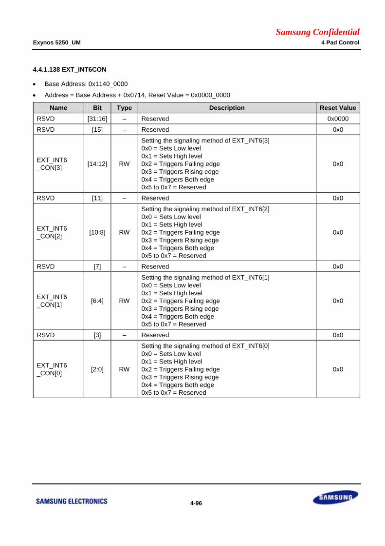
Samsung Confidential Exynos 5250_UM 4 Pad Control
4-96
4.4.1.138 EXT_INT6CON
Base Address: 0x1140_0000
Address = Base Address + 0x0714, Reset Value = 0x0000_0000
Name Bit Type Description Reset Value
RSVD [31:16] – Reserved 0x0000
RSVD [15] – Reserved 0x0
EXT_INT6
_CON[3] [14:12] RW
Setting the signaling method of EXT_INT6[3]
0x0 = Sets Low level
0x1 = Sets High level
0x2 = Triggers Falling edge
0x3 = Triggers Rising edge
0x4 = Triggers Both edge
0x5 to 0x7 = Reserved
0x0
RSVD [11] – Reserved 0x0
EXT_INT6
_CON[2] [10:8] RW
Setting the signaling method of EXT_INT6[2]
0x0 = Sets Low level
0x1 = Sets High level
0x2 = Triggers Falling edge
0x3 = Triggers Rising edge
0x4 = Triggers Both edge
0x5 to 0x7 = Reserved
0x0
RSVD [7] – Reserved 0x0
EXT_INT6
_CON[1] [6:4] RW
Setting the signaling method of EXT_INT6[1]
0x0 = Sets Low level
0x1 = Sets High level
0x2 = Triggers Falling edge
0x3 = Triggers Rising edge
0x4 = Triggers Both edge
0x5 to 0x7 = Reserved
0x0
RSVD [3] – Reserved 0x0
EXT_INT6
_CON[0] [2:0] RW
Setting the signaling method of EXT_INT6[0]
0x0 = Sets Low level
0x1 = Sets High level
0x2 = Triggers Falling edge
0x3 = Triggers Rising edge
0x4 = Triggers Both edge
0x5 to 0x7 = Reserved
0x0

Samsung Confidential Exynos 5250_UM 4 Pad Control
4-97
4.4.1.139 EXT_INT7CON
Base Address: 0x1140_0000
Address = Base Address + 0x0718, Reset Value = 0x0000_0000
Name Bit Type Description Reset Value
RSVD [31:16] – Reserved 0x0000
RSVD [15] – Reserved 0x0
EXT_INT7
_CON[3] [14:12] RW
Setting the signaling method of EXT_INT7[3]
0x0 = Sets Low level
0x1 = Sets High level
0x2 = Triggers Falling edge
0x3 = Triggers Rising edge
0x4 = Triggers Both edge
0x5 to 0x7 = Reserved
0x0
RSVD [11] – Reserved 0x0
EXT_INT7
_CON[2] [10:8] RW
Setting the signaling method of EXT_INT7[2]
0x0 = Sets Low level
0x1 = Sets High level
0x2 = Triggers Falling edge
0x3 = Triggers Rising edge
0x4 = Triggers Both edge
0x5 to 0x7 = Reserved
0x0
RSVD [7] – Reserved 0x0
EXT_INT7
_CON[1] [6:4] RW
Setting the signaling method of EXT_INT7[1]
0x0 = Sets Low level
0x1 = Sets High level
0x2 = Triggers Falling edge
0x3 = Triggers Rising edge
0x4 = Triggers Both edge
0x5 to 0x7 = Reserved
0x0
RSVD [3] – Reserved 0x0
EXT_INT7
_CON[0] [2:0] RW
Setting the signaling method of EXT_INT7[0]
0x0 = Sets Low level
0x1 = Sets High level
0x2 = Triggers Falling edge
0x3 = Triggers Rising edge
0x4 = Triggers Both edge
0x5 to 0x7 = Reserved
0x0
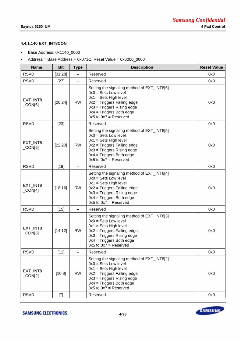
Samsung Confidential Exynos 5250_UM 4 Pad Control
4-98
4.4.1.140 EXT_INT8CON
Base Address: 0x1140_0000
Address = Base Address + 0x071C, Reset Value = 0x0000_0000
Name Bit Type Description Reset Value
RSVD [31:28] – Reserved 0x0
RSVD [27] – Reserved 0x0
EXT_INT8
_CON[6] [26:24] RW
Setting the signaling method of EXT_INT8[6]
0x0 = Sets Low level
0x1 = Sets High level
0x2 = Triggers Falling edge
0x3 = Triggers Rising edge
0x4 = Triggers Both edge
0x5 to 0x7 = Reserved
0x0
RSVD [23] – Reserved 0x0
EXT_INT8
_CON[5] [22:20] RW
Setting the signaling method of EXT_INT8[5]
0x0 = Sets Low level
0x1 = Sets High level
0x2 = Triggers Falling edge
0x3 = Triggers Rising edge
0x4 = Triggers Both edge
0x5 to 0x7 = Reserved
0x0
RSVD [19] – Reserved 0x0
EXT_INT8
_CON[4] [18:16] RW
Setting the signaling method of EXT_INT8[4]
0x0 = Sets Low level
0x1 = Sets High level
0x2 = Triggers Falling edge
0x3 = Triggers Rising edge
0x4 = Triggers Both edge
0x5 to 0x7 = Reserved
0x0
RSVD [15] – Reserved 0x0
EXT_INT8
_CON[3] [14:12] RW
Setting the signaling method of EXT_INT8[3]
0x0 = Sets Low level
0x1 = Sets High level
0x2 = Triggers Falling edge
0x3 = Triggers Rising edge
0x4 = Triggers Both edge
0x5 to 0x7 = Reserved
0x0
RSVD [11] – Reserved 0x0
EXT_INT8
_CON[2] [10:8] RW
Setting the signaling method of EXT_INT8[2]
0x0 = Sets Low level
0x1 = Sets High level
0x2 = Triggers Falling edge
0x3 = Triggers Rising edge
0x4 = Triggers Both edge
0x5 to 0x7 = Reserved
0x0
RSVD [7] – Reserved 0x0
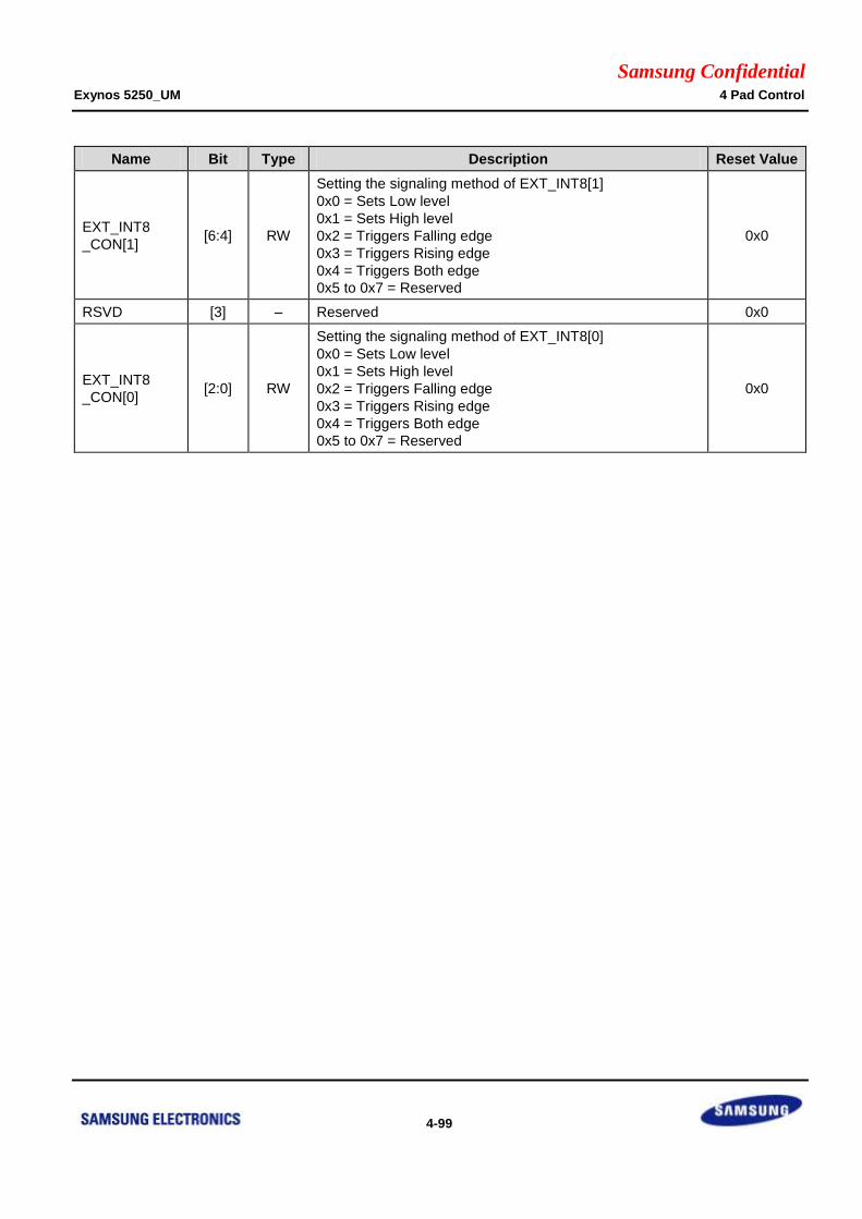
Samsung Confidential Exynos 5250_UM 4 Pad Control
4-99
Name Bit Type Description Reset Value
EXT_INT8
_CON[1] [6:4] RW
Setting the signaling method of EXT_INT8[1]
0x0 = Sets Low level
0x1 = Sets High level
0x2 = Triggers Falling edge
0x3 = Triggers Rising edge
0x4 = Triggers Both edge
0x5 to 0x7 = Reserved
0x0
RSVD [3] – Reserved 0x0
EXT_INT8
_CON[0] [2:0] RW
Setting the signaling method of EXT_INT8[0]
0x0 = Sets Low level
0x1 = Sets High level
0x2 = Triggers Falling edge
0x3 = Triggers Rising edge
0x4 = Triggers Both edge
0x5 to 0x7 = Reserved
0x0

Samsung Confidential Exynos 5250_UM 4 Pad Control
4-100
4.4.1.141 EXT_INT9CON
Base Address: 0x1140_0000
Address = Base Address + 0x0720, Reset Value = 0x0000_0000
Name Bit Type Description Reset Value
RSVD [31:16] – Reserved 0x0000
RSVD [15] – Reserved 0x0
EXT_INT9
_CON[3] [14:12] RW
Setting the signaling method of EXT_INT9[3]
0x0 = Sets Low level
0x1 = Sets High level
0x2 = Triggers Falling edge
0x3 = Triggers Rising edge
0x4 = Triggers Both edge
0x5 to 0x7 = Reserved
0x0
RSVD [11] – Reserved 0x0
EXT_INT9
_CON[2] [10:8] RW
Setting the signaling method of EXT_INT9[2]
0x0 = Sets Low level
0x1 = Sets High level
0x2 = Triggers Falling edge
0x3 = Triggers Rising edge
0x4 = Triggers Both edge
0x5 to 0x7 = Reserved
0x0
RSVD [7] – Reserved 0x0
EXT_INT9
_CON[1] [6:4] RW
Setting the signaling method of EXT_INT9[1]
0x0 = Sets Low level
0x1 = Sets High level
0x2 = Triggers Falling edge
0x3 = Triggers Rising edge
0x4 = Triggers Both edge
0x5 to 0x7 = Reserved
0x0
RSVD [3] – Reserved 0x0
EXT_INT9
_CON[0] [2:0] RW
Setting the signaling method of EXT_INT9[0]
0x0 = Sets Low level
0x1 = Sets High level
0x2 = Triggers Falling edge
0x3 = Triggers Rising edge
0x4 = Triggers Both edge
0x5 to 0x7 = Reserved
0x0

Samsung Confidential Exynos 5250_UM 4 Pad Control
4-101
4.4.1.142 EXT_INT10CON
Base Address: 0x1140_0000
Address = Base Address + 0x0724, Reset Value = 0x0000_0000
Name Bit Type Description Reset Value
RSVD [31:28] – Reserved 0x0
RSVD [27] – Reserved 0x0
EXT_INT10
_CON[6] [26:24] RW
Setting the signaling method of EXT_INT10[6]
0x0 = Sets Low level
0x1 = Sets High level
0x2 = Triggers Falling edge
0x3 = Triggers Rising edge
0x4 = Triggers Both edge
0x5 to 0x7 = Reserved
0x0
RSVD [23] – Reserved 0x0
EXT_INT10
_CON[5] [22:20] RW
Setting the signaling method of EXT_INT10[5]
0x0 = Sets Low level
0x1 = Sets High level
0x2 = Triggers Falling edge
0x3 = Triggers Rising edge
0x4 = Triggers Both edge
0x5 to 0x7 = Reserved
0x0
RSVD [19] – Reserved 0x0
EXT_INT10
_CON[4] [18:16] RW
Setting the signaling method of EXT_INT10[4]
0x0 = Sets Low level
0x1 = Sets High level
0x2 = Triggers Falling edge
0x3 = Triggers Rising edge
0x4 = Triggers Both edge
0x5 to 0x7 = Reserved
0x0
RSVD [15] – Reserved 0x0
EXT_INT10
_CON[3] [14:12] RW
Setting the signaling method of EXT_INT10[3]
0x0 = Sets Low level
0x1 = Sets High level
0x2 = Triggers Falling edge
0x3 = Triggers Rising edge
0x4 = Triggers Both edge
0x5 to 0x7 = Reserved
0x0
RSVD [11] – Reserved 0x0
EXT_INT10
_CON[2] [10:8] RW
Setting the signaling method of EXT_INT10[2]
0x0 = Sets Low level
0x1 = Sets High level
0x2 = Triggers Falling edge
0x3 = Triggers Rising edge
0x4 = Triggers Both edge
0x5 to 0x7 = Reserved
0x0
RSVD [7] – Reserved 0x0

Samsung Confidential Exynos 5250_UM 4 Pad Control
4-102
Name Bit Type Description Reset Value
EXT_INT10
_CON[1] [6:4] RW
Setting the signaling method of EXT_INT10[1]
0x0 = Sets Low level
0x1 = Sets High level
0x2 = Triggers Falling edge
0x3 = Triggers Rising edge
0x4 = Triggers Both edge
0x5 to 0x7 = Reserved
0x0
RSVD [3] – Reserved 0x0
EXT_INT10
_CON[0] [2:0] RW
Setting the signaling method of EXT_INT10[0]
0x0 = Sets Low level
0x1 = Sets High level
0x2 = Triggers Falling edge
0x3 = Triggers Rising edge
0x4 = Triggers Both edge
0x5 to 0x7 = Reserved
0x0

Samsung Confidential Exynos 5250_UM 4 Pad Control
4-103
4.4.1.143 EXT_INT11CON
Base Address: 0x1140_0000
Address = Base Address + 0x0728, Reset Value = 0x0000_0000
Name Bit Type Description Reset Value
RSVD [31:28] – Reserved 0x0
RSVD [27] – Reserved 0x0
EXT_INT11
_CON[6] [26:24] RW
Setting the signaling method of EXT_INT11[6]
0x0 = Sets Low level
0x1 = Sets High level
0x2 = Triggers Falling edge
0x3 = Triggers Rising edge
0x4 = Triggers Both edge
0x5 to 0x7 = Reserved
0x0
RSVD [23] – Reserved 0x0
EXT_INT11
_CON[5] [22:20] RW
Setting the signaling method of EXT_INT11[5]
0x0 = Sets Low level
0x1 = Sets High level
0x2 = Triggers Falling edge
0x3 = Triggers Rising edge
0x4 = Triggers Both edge
0x5 to 0x7 = Reserved
0x0
RSVD [19] – Reserved 0x0
EXT_INT11
_CON[4] [18:16] RW
Setting the signaling method of EXT_INT11[4]
0x0 = Sets Low level
0x1 = Sets High level
0x2 = Triggers Falling edge
0x3 = Triggers Rising edge
0x4 = Triggers Both edge
0x5 to 0x7 = Reserved
0x0
RSVD [15] – Reserved 0x0
EXT_INT11
_CON[3] [14:12] RW
Setting the signaling method of EXT_INT11[3]
0x0 = Sets Low level
0x1 = Sets High level
0x2 = Triggers Falling edge
0x3 = Triggers Rising edge
0x4 = Triggers Both edge
0x5 to 0x7 = Reserved
0x0
RSVD [11] – Reserved 0x0
EXT_INT11
_CON[2] [10:8] RW
Setting the signaling method of EXT_INT11[2]
0x0 = Sets Low level
0x1 = Sets High level
0x2 = Triggers Falling edge
0x3 = Triggers Rising edge
0x4 = Triggers Both edge
0x5 to 0x7 = Reserved
0x0
RSVD [7] – Reserved 0x0

Samsung Confidential Exynos 5250_UM 4 Pad Control
4-104
Name Bit Type Description Reset Value
EXT_INT11
_CON[1] [6:4] RW
Setting the signaling method of EXT_INT11[1]
0x0 = Sets Low level
0x1 = Sets High level
0x2 = Triggers Falling edge
0x3 = Triggers Rising edge
0x4 = Triggers Both edge
0x5 to 0x7 = Reserved
0x0
RSVD [3] – Reserved 0x0
EXT_INT11
_CON[0] [2:0] RW
Setting the signaling method of EXT_INT11[0]
0x0 = Sets Low level
0x1 = Sets High level
0x2 = Triggers Falling edge
0x3 = Triggers Rising edge
0x4 = Triggers Both edge
0x5 to 0x7 = Reserved
0x0

Samsung Confidential Exynos 5250_UM 4 Pad Control
4-105
4.4.1.144 EXT_INT12CON
Base Address: 0x1140_0000
Address = Base Address + 0x072C, Reset Value = 0x0000_0000
Name Bit Type Description Reset Value
RSVD [31:16] – Reserved 0x0000
RSVD [15] – Reserved 0x0
EXT_INT12
_CON[3] [14:12] RW
Setting the signaling method of EXT_INT12[3]
0x0 = Sets Low level
0x1 = Sets High level
0x2 = Triggers Falling edge
0x3 = Triggers Rising edge
0x4 = Triggers Both edge
0x5 to 0x7 = Reserved
0x0
RSVD [11] – Reserved 0x0
EXT_INT12
_CON[2] [10:8] RW
Setting the signaling method of EXT_INT12[2]
0x0 = Sets Low level
0x1 = Sets High level
0x2 = Triggers Falling edge
0x3 = Triggers Rising edge
0x4 = Triggers Both edge
0x5 to 0x7 = Reserved
0x0
RSVD [7] – Reserved 0x0
EXT_INT12
_CON[1] [6:4] RW
Setting the signaling method of EXT_INT12[1]
0x0 = Sets Low level
0x1 = Sets High level
0x2 = Triggers Falling edge
0x3 = Triggers Rising edge
0x4 = Triggers Both edge
0x5 to 0x7 = Reserved
0x0
RSVD [3] – Reserved 0x0
EXT_INT12
_CON[0] [2:0] RW
Setting the signaling method of EXT_INT12[0]
0x0 = Sets Low level
0x1 = Sets High level
0x2 = Triggers Falling edge
0x3 = Triggers Rising edge
0x4 = Triggers Both edge
0x5 to 0x7 = Reserved
0x0

Samsung Confidential Exynos 5250_UM 4 Pad Control
4-106
4.4.1.145 EXT_INT13CON
Base Address: 0x1140_0000
Address = Base Address + 0x0730, Reset Value = 0x0000_0000
Name Bit Type Description Reset Value
RSVD [31] – Reserved 0x0
EXT_INT13
_CON[7] [30:28] RW
Setting the signaling method of EXT_INT13[7]
0x0 = Sets Low level
0x1 = Sets High level
0x2 = Triggers Falling edge
0x3 = Triggers Rising edge
0x4 = Triggers Both edge
0x5 to 0x7 = Reserved
0x0
RSVD [27] – Reserved 0x0
EXT_INT13
_CON[6] [26:24] RW
Setting the signaling method of EXT_INT13[6]
0x0 = Sets Low level
0x1 = Sets High level
0x2 = Triggers Falling edge
0x3 = Triggers Rising edge
0x4 = Triggers Both edge
0x5 to 0x7 = Reserved
0x0
RSVD [23] – Reserved 0x0
EXT_INT13
_CON[5] [22:20] RW
Setting the signaling method of EXT_INT13[5]
0x0 = Sets Low level
0x1 = Sets High level
0x2 = Triggers Falling edge
0x3 = Triggers Rising edge
0x4 = Triggers Both edge
0x5 to 0x7 = Reserved
0x0
RSVD [19] – Reserved 0x0
EXT_INT13
_CON[4] [18:16] RW
Setting the signaling method of EXT_INT13[4]
0x0 = Sets Low level
0x1 = Sets High level
0x2 = Triggers Falling edge
0x3 = Triggers Rising edge
0x4 = Triggers Both edge
0x5 to 0x7 = Reserved
0x0
RSVD [15] – Reserved 0x0
EXT_INT13
_CON[3] [14:12] RW
Setting the signaling method of EXT_INT13[3]
0x0 = Sets Low level
0x1 = Sets High level
0x2 = Triggers Falling edge
0x3 = Triggers Rising edge
0x4 = Triggers Both edge
0x5 to 0x7 = Reserved
0x0
RSVD [11] – Reserved 0x0
EXT_INT13 [10:8] RW Setting the signaling method of EXT_INT13[2] 0x0
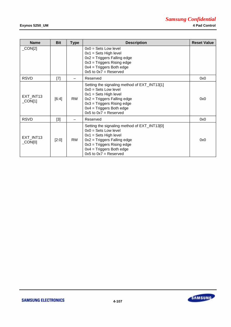
Samsung Confidential Exynos 5250_UM 4 Pad Control
4-107
Name Bit Type Description Reset Value
_CON[2] 0x0 = Sets Low level
0x1 = Sets High level
0x2 = Triggers Falling edge
0x3 = Triggers Rising edge
0x4 = Triggers Both edge
0x5 to 0x7 = Reserved
RSVD [7] – Reserved 0x0
EXT_INT13
_CON[1] [6:4] RW
Setting the signaling method of EXT_INT13[1]
0x0 = Sets Low level
0x1 = Sets High level
0x2 = Triggers Falling edge
0x3 = Triggers Rising edge
0x4 = Triggers Both edge
0x5 to 0x7 = Reserved
0x0
RSVD [3] – Reserved 0x0
EXT_INT13
_CON[0] [2:0] RW
Setting the signaling method of EXT_INT13[0]
0x0 = Sets Low level
0x1 = Sets High level
0x2 = Triggers Falling edge
0x3 = Triggers Rising edge
0x4 = Triggers Both edge
0x5 to 0x7 = Reserved
0x0

Samsung Confidential Exynos 5250_UM 4 Pad Control
4-108
4.4.1.146 EXT_INT30CON
Base Address: 0x1140_0000
Address = Base Address + 0x0734, Reset Value = 0x0000_0000
Name Bit Type Description Reset Value
RSVD [31:28] – Reserved 0x0
RSVD [27] – Reserved 0x0
EXT_INT13
_CON[6] [26:24] RW
Setting the signaling method of EXT_INT30[6]
0x0 = Sets Low level
0x1 = Sets High level
0x2 = Triggers Falling edge
0x3 = Triggers Rising edge
0x4 = Triggers Both edge
0x5 to 0x7 = Reserved
0x0
RSVD [23] – Reserved 0x0
EXT_INT13
_CON[5] [22:20] RW
Setting the signaling method of EXT_INT30[5]
0x0 = Sets Low level
0x1 = Sets High level
0x2 = Triggers Falling edge
0x3 = Triggers Rising edge
0x4 = Triggers Both edge
0x5 to 0x7 = Reserved
0x0
RSVD [19] – Reserved 0x0
EXT_INT13
_CON[4] [18:16] RW
Setting the signaling method of EXT_INT30[4]
0x0 = Sets Low level
0x1 = Sets High level
0x2 = Triggers Falling edge
0x3 = Triggers Rising edge
0x4 = Triggers Both edge
0x5 to 0x7 = Reserved
0x0
RSVD [15] – Reserved 0x0
EXT_INT13
_CON[3] [14:12] RW
Setting the signaling method of EXT_INT30[3]
0x0 = Sets Low level
0x1 = Sets High level
0x2 = Triggers Falling edge
0x3 = Triggers Rising edge
0x4 = Triggers Both edge
0x5 to 0x7 = Reserved
0x0
RSVD [11] – Reserved 0x0
EXT_INT13
_CON[2] [10:8] RW
Setting the signaling method of EXT_INT30[2]
0x0 = Sets Low level
0x1 = Sets High level
0x2 = Triggers Falling edge
0x3 = Triggers Rising edge
0x4 = Triggers Both edge
0x5 to 0x7 = Reserved
0x0
RSVD [7] – Reserved 0x0

Samsung Confidential Exynos 5250_UM 4 Pad Control
4-109
Name Bit Type Description Reset Value
EXT_INT13
_CON[1] [6:4] RW
Setting the signaling method of EXT_INT30[1]
0x0 = Sets Low level
0x1 = Sets High level
0x2 = Triggers Falling edge
0x3 = Triggers Rising edge
0x4 = Triggers Both edge
0x5 to 0x7 = Reserved
0x0
RSVD [3] – Reserved 0x0
EXT_INT13
_CON[0] [2:0] RW
Setting the signaling method of EXT_INT30[0]
0x0 = Sets Low level
0x1 = Sets High level
0x2 = Triggers Falling edge
0x3 = Triggers Rising edge
0x4 = Triggers Both edge
0x5 to 0x7 = Reserved
0x0

Samsung Confidential Exynos 5250_UM 4 Pad Control
4-110
4.4.1.147 EXT_INT1_FLTCON0
Base Address: 0x1140_0000
Address = Base Address + 0x0800, Reset Value = 0x0000_0000
Name Bit Type Description Reset Value
FLTEN1[3] [31] RW
Enables Filter for EXT_INT1[3]
0x0 = Disables
0x1 = Enables
0x0
FLTWIDTH1[3] [30:24] RW Filtering width of EXT_INT1[3] 0x00
FLTEN1[2] [23] RW
Enables Filter for EXT_INT1[2]
0x0 = Disables
0x1 = Enables
0x0
FLTWIDTH1[2] [22:16] RW Filtering width of EXT_INT1[2] 0x00
FLTEN1[1] [15] RW
Enables Filter for EXT_INT1[1]
0x0 = Disables
0x1 = Enables
0x0
FLTWIDTH1[1] [14:8] RW Filtering width of EXT_INT1[1] 0x00
FLTEN1[0] [7] RW
Enables Filter for EXT_INT1[0]
0x0 = Disables
0x1 = Enables
0x0
FLTWIDTH1[0] [6:0] RW Filtering width of EXT_INT1[0] 0x00

Samsung Confidential Exynos 5250_UM 4 Pad Control
4-111
4.4.1.148 EXT_INT1_FLTCON1
Base Address: 0x1140_0000
Address = Base Address + 0x0804, Reset Value = 0x0000_0000
Name Bit Type Description Reset Value
FLTEN1[7] [31] RW
Enables Filter for EXT_INT1[7]
0x0 = Disables
0x1 = Enables
0x0
FLTWIDTH1[7] [30:24] RW Filtering width of EXT_INT1[7] 0x00
FLTEN1[6] [23] RW
Enables Filter for EXT_INT1[6]
0x0 = Disables
0x1 = Enables
0x0
FLTWIDTH1[6] [22:16] RW Filtering width of EXT_INT1[6] 0x00
FLTEN1[5] [15] RW
Enables Filter for EXT_INT1[5]
0x0 = Disables
0x1 = Enables
0x0
FLTWIDTH1[5] [14:8] RW Filtering width of EXT_INT1[5] 0x00
FLTEN1[4] [7] RW
Enables Filter for EXT_INT1[4]
0x0 = Disables
0x1 = Enables
0x0
FLTWIDTH1[4] [6:0] RW Filtering width of EXT_INT1[4] 0x00
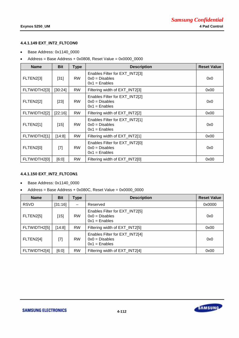
Samsung Confidential Exynos 5250_UM 4 Pad Control
4-112
4.4.1.149 EXT_INT2_FLTCON0
Base Address: 0x1140_0000
Address = Base Address + 0x0808, Reset Value = 0x0000_0000
Name Bit Type Description Reset Value
FLTEN2[3] [31] RW
Enables Filter for EXT_INT2[3]
0x0 = Disables
0x1 = Enables
0x0
FLTWIDTH2[3] [30:24] RW Filtering width of EXT_INT2[3] 0x00
FLTEN2[2] [23] RW
Enables Filter for EXT_INT2[2]
0x0 = Disables
0x1 = Enables
0x0
FLTWIDTH2[2] [22:16] RW Filtering width of EXT_INT2[2] 0x00
FLTEN2[1] [15] RW
Enables Filter for EXT_INT2[1]
0x0 = Disables
0x1 = Enables
0x0
FLTWIDTH2[1] [14:8] RW Filtering width of EXT_INT2[1] 0x00
FLTEN2[0] [7] RW
Enables Filter for EXT_INT2[0]
0x0 = Disables
0x1 = Enables
0x0
FLTWIDTH2[0] [6:0] RW Filtering width of EXT_INT2[0] 0x00
4.4.1.150 EXT_INT2_FLTCON1
Base Address: 0x1140_0000
Address = Base Address + 0x080C, Reset Value = 0x0000_0000
Name Bit Type Description Reset Value
RSVD [31:16] – Reserved 0x0000
FLTEN2[5] [15] RW
Enables Filter for EXT_INT2[5]
0x0 = Disables
0x1 = Enables
0x0
FLTWIDTH2[5] [14:8] RW Filtering width of EXT_INT2[5] 0x00
FLTEN2[4] [7] RW
Enables Filter for EXT_INT2[4]
0x0 = Disables
0x1 = Enables
0x0
FLTWIDTH2[4] [6:0] RW Filtering width of EXT_INT2[4] 0x00

Samsung Confidential Exynos 5250_UM 4 Pad Control
4-113
4.4.1.151 EXT_INT3_FLTCON0
Base Address: 0x1140_0000
Address = Base Address + 0x0810, Reset Value = 0x0000_0000
Name Bit Type Description Reset Value
FLTEN3[3] [31] RW
Enables Filter for EXT_INT3[3]
0x0 = Disables
0x1 = Enables
0x0
FLTWIDTH3[3] [30:24] RW Filtering width of EXT_INT3[3] 0x00
FLTEN3[2] [23] RW
Enables Filter for EXT_INT3[2]
0x0 = Disables
0x1 = Enables
0x0
FLTWIDTH3[2] [22:16] RW Filtering width of EXT_INT3[2] 0x00
FLTEN3[1] [15] RW
Enables Filter for EXT_INT3[1]
0x0 = Disables
0x1 = Enables
0x0
FLTWIDTH3[1] [14:8] RW Filtering width of EXT_INT3[1] 0x00
FLTEN3[0] [7] RW
Enables Filter for EXT_INT3[0]
0x0 = Disables
0x1 = Enables
0x0
FLTWIDTH3[0] [6:0] RW Filtering width of EXT_INT3[0] 0x00
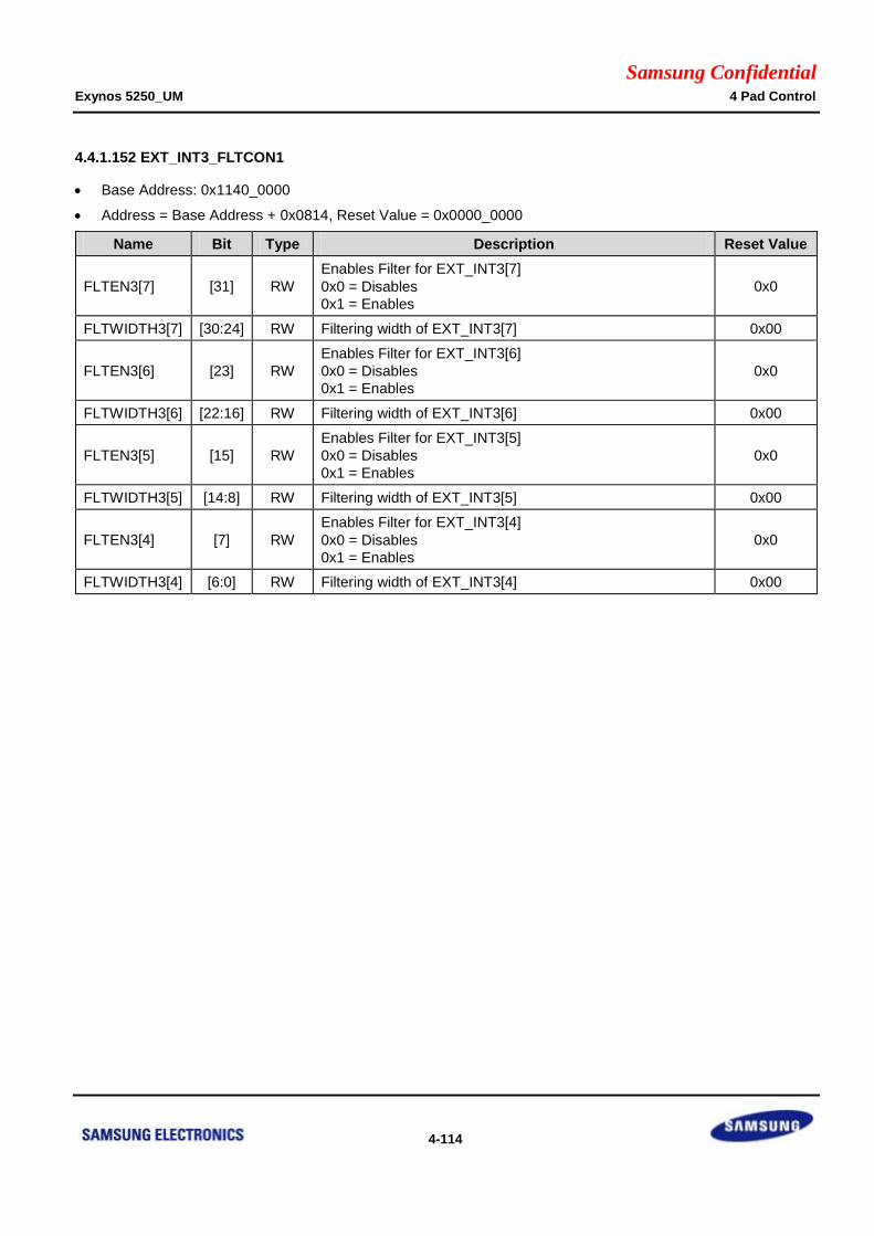
Samsung Confidential Exynos 5250_UM 4 Pad Control
4-114
4.4.1.152 EXT_INT3_FLTCON1
Base Address: 0x1140_0000
Address = Base Address + 0x0814, Reset Value = 0x0000_0000
Name Bit Type Description Reset Value
FLTEN3[7] [31] RW
Enables Filter for EXT_INT3[7]
0x0 = Disables
0x1 = Enables
0x0
FLTWIDTH3[7] [30:24] RW Filtering width of EXT_INT3[7] 0x00
FLTEN3[6] [23] RW
Enables Filter for EXT_INT3[6]
0x0 = Disables
0x1 = Enables
0x0
FLTWIDTH3[6] [22:16] RW Filtering width of EXT_INT3[6] 0x00
FLTEN3[5] [15] RW
Enables Filter for EXT_INT3[5]
0x0 = Disables
0x1 = Enables
0x0
FLTWIDTH3[5] [14:8] RW Filtering width of EXT_INT3[5] 0x00
FLTEN3[4] [7] RW
Enables Filter for EXT_INT3[4]
0x0 = Disables
0x1 = Enables
0x0
FLTWIDTH3[4] [6:0] RW Filtering width of EXT_INT3[4] 0x00

Samsung Confidential Exynos 5250_UM 4 Pad Control
4-115
4.4.1.153 EXT_INT4_FLTCON0
Base Address: 0x1140_0000
Address = Base Address + 0x0818, Reset Value = 0x0000_0000
Name Bit Type Description Reset Value
FLTEN4[3] [31] RW
Enables Filter for EXT_INT4[3]
0x0 = Disables
0x1 = Enables
0x0
FLTWIDTH4[3] [30:24] RW Filtering width of EXT_INT4[3] 0x00
FLTEN4[2] [23] RW
Enables Filter for EXT_INT4[2]
0x0 = Disables
0x1 = Enables
0x0
FLTWIDTH4[2] [22:16] RW Filtering width of EXT_INT4[2] 0x00
FLTEN4[1] [15] RW
Enables Filter for EXT_INT4[1]
0x0 = Disables
0x1 = Enables
0x0
FLTWIDTH4[1] [14:8] RW Filtering width of EXT_INT4[1] 0x00
FLTEN4[0] [7] RW
Enables Filter for EXT_INT4[0]
0x0 = Disables
0x1 = Enables
0x0
FLTWIDTH4[0] [6:0] RW Filtering width of EXT_INT4[0] 0x00
4.4.1.154 EXT_INT4_FLTCON1
Base Address: 0x1140_0000
Address = Base Address + 0x081C, Reset Value = 0x0000_0000
Name Bit Type Description Reset Value
RSVD [31:8] – Reserved 0x000000
FLTEN4[4] [7] RW
Enables Filter for EXT_INT4[4]
0x0 = Disables
0x1 = Enables
0x0
FLTWIDTH4[4] [6:0] RW Filtering width of EXT_INT4[4] 0x00
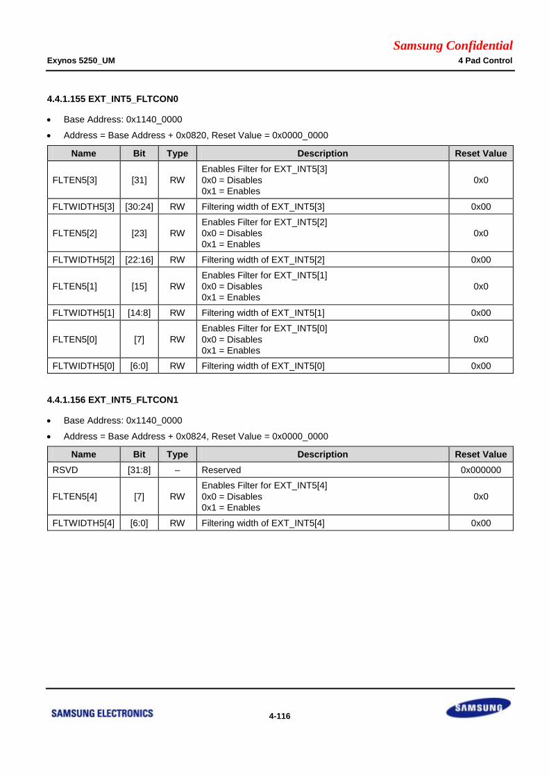
Samsung Confidential Exynos 5250_UM 4 Pad Control
4-116
4.4.1.155 EXT_INT5_FLTCON0
Base Address: 0x1140_0000
Address = Base Address + 0x0820, Reset Value = 0x0000_0000
Name Bit Type Description Reset Value
FLTEN5[3] [31] RW
Enables Filter for EXT_INT5[3]
0x0 = Disables
0x1 = Enables
0x0
FLTWIDTH5[3] [30:24] RW Filtering width of EXT_INT5[3] 0x00
FLTEN5[2] [23] RW
Enables Filter for EXT_INT5[2]
0x0 = Disables
0x1 = Enables
0x0
FLTWIDTH5[2] [22:16] RW Filtering width of EXT_INT5[2] 0x00
FLTEN5[1] [15] RW
Enables Filter for EXT_INT5[1]
0x0 = Disables
0x1 = Enables
0x0
FLTWIDTH5[1] [14:8] RW Filtering width of EXT_INT5[1] 0x00
FLTEN5[0] [7] RW
Enables Filter for EXT_INT5[0]
0x0 = Disables
0x1 = Enables
0x0
FLTWIDTH5[0] [6:0] RW Filtering width of EXT_INT5[0] 0x00
4.4.1.156 EXT_INT5_FLTCON1
Base Address: 0x1140_0000
Address = Base Address + 0x0824, Reset Value = 0x0000_0000
Name Bit Type Description Reset Value
RSVD [31:8] – Reserved 0x000000
FLTEN5[4] [7] RW
Enables Filter for EXT_INT5[4]
0x0 = Disables
0x1 = Enables
0x0
FLTWIDTH5[4] [6:0] RW Filtering width of EXT_INT5[4] 0x00

Samsung Confidential Exynos 5250_UM 4 Pad Control
4-117
4.4.1.157 EXT_INT6_FLTCON0
Base Address: 0x1140_0000
Address = Base Address + 0x0828, Reset Value = 0x0000_0000
Name Bit Type Description Reset Value
FLTEN6[3] [31] RW
Enables Filter for EXT_INT6[3]
0x0 = Disables
0x1 = Enables
0x0
FLTWIDTH6[3] [30:24] RW Filtering width of EXT_INT6[3] 0x00
FLTEN6[2] [23] RW
Enables Filter for EXT_INT6[2]
0x0 = Disables
0x1 = Enables
0x0
FLTWIDTH6[2] [22:16] RW Filtering width of EXT_INT6[2] 0x00
FLTEN6[1] [15] RW
Enables Filter for EXT_INT6[1]
0x0 = Disables
0x1 = Enables
0x0
FLTWIDTH6[1] [14:8] RW Filtering width of EXT_INT6[1] 0x00
FLTEN6[0] [7] RW
Enables Filter for EXT_INT6[0]
0x0 = Disables
0x1 = Enables
0x0
FLTWIDTH6[0] [6:0] RW Filtering width of EXT_INT6[0] 0x00
4.4.1.158 EXT_INT6_FLTCON1
Base Address: 0x1140_0000
Address = Base Address + 0x082C, Reset Value = 0x0000_0000
Name Bit Type Description Reset Value
RSVD [31:0] – Reserved 0x00000000

Samsung Confidential Exynos 5250_UM 4 Pad Control
4-118
4.4.1.159 EXT_INT7_FLTCON0
Base Address: 0x1140_0000
Address = Base Address + 0x0830, Reset Value = 0x0000_0000
Name Bit Type Description Reset Value
FLTEN7[3] [31] RW
Enables Filter for EXT_INT7[3]
0x0 = Disables
0x1 = Enables
0x0
FLTWIDTH7[3] [30:24] RW Filtering width of EXT_INT7[3] 0x00
FLTEN7[2] [23] RW
Enables Filter for EXT_INT7[2]
0x0 = Disables
0x1 = Enables
0x0
FLTWIDTH7[2] [22:16] RW Filtering width of EXT_INT7[2] 0x00
FLTEN7[1] [15] RW
Enables Filter for EXT_INT7[1]
0x0 = Disables
0x1 = Enables
0x0
FLTWIDTH7[1] [14:8] RW Filtering width of EXT_INT7[1] 0x00
FLTEN7[0] [7] RW
Enables Filter for EXT_INT7[0]
0x0 = Disables
0x1 = Enables
0x0
FLTWIDTH7[0] [6:0] RW Filtering width of EXT_INT7[0] 0x00
4.4.1.160 EXT_INT7_FLTCON1
Base Address: 0x1140_0000
Address = Base Address + 0x0834, Reset Value = 0x0000_0000
Name Bit Type Description Reset Value
RSVD [31:0] – Reserved 0x00000000

Samsung Confidential Exynos 5250_UM 4 Pad Control
4-119
4.4.1.161 EXT_INT8_FLTCON0
Base Address: 0x1140_0000
Address = Base Address + 0x0838, Reset Value = 0x0000_0000
Name Bit Type Description Reset Value
FLTEN8[3] [31] RW
Enables Filter for EXT_INT8[3]
0x0 = Disables
0x1 = Enables
0x0
FLTWIDTH8[3] [30:24] RW Filtering width of EXT_INT8[3] 0x00
FLTEN8[2] [23] RW
Enables Filter for EXT_INT8[2]
0x0 = Disables
0x1 = Enables
0x0
FLTWIDTH8[2] [22:16] RW Filtering width of EXT_INT8[2] 0x00
FLTEN8[1] [15] RW
Enables Filter for EXT_INT8[1]
0x0 = Disables
0x1 = Enables
0x0
FLTWIDTH8[1] [14:8] RW Filtering width of EXT_INT8[1] 0x00
FLTEN8[0] [7] RW
Enables Filter for EXT_INT8[0]
0x0 = Disables
0x1 = Enables
0x0
FLTWIDTH8[0] [6:0] RW Filtering width of EXT_INT8[0] 0x00

Samsung Confidential Exynos 5250_UM 4 Pad Control
4-120
4.4.1.162 EXT_INT8_FLTCON1
Base Address: 0x1140_0000
Address = Base Address + 0x083C, Reset Value = 0x0000_0000
Name Bit Type Description Reset Value
FLTEN8[3] [31] RW
Enables Filter for EXT_INT8[3]
0x0 = Disables
0x1 = Enables
0x0
FLTWIDTH8[3] [30:24] RW Filtering width of EXT_INT8[3] 0x00
FLTEN8[2] [23] RW
Enables Filter for EXT_INT8[2]
0x0 = Disables
0x1 = Enables
0x0
FLTWIDTH8[2] [22:16] RW Filtering width of EXT_INT8[2] 0x00
FLTEN8[1] [15] RW
Enables Filter for EXT_INT8[1]
0x0 = Disables
0x1 = Enables
0x0
FLTWIDTH8[1] [14:8] RW Filtering width of EXT_INT8[1] 0x00
FLTEN8[0] [7] RW
Enables Filter for EXT_INT8[0]
0x0 = Disables
0x1 = Enables
0x0
FLTWIDTH8[0] [6:0] RW Filtering width of EXT_INT8[0] 0x00

Samsung Confidential Exynos 5250_UM 4 Pad Control
4-121
4.4.1.163 EXT_INT9_FLTCON0
Base Address: 0x1140_0000
Address = Base Address + 0x0840, Reset Value = 0x0000_0000
Name Bit Type Description Reset Value
FLTEN9[3] [31] RW
Enables Filter for EXT_INT9[3]
0x0 = Disables
0x1 = Enables
0x0
FLTWIDTH9[3] [30:24] RW Filtering width of EXT_INT9[3] 0x00
FLTEN9[2] [23] RW
Enables Filter for EXT_INT9[2]
0x0 = Disables
0x1 = Enables
0x0
FLTWIDTH9[2] [22:16] RW Filtering width of EXT_INT9[2] 0x00
FLTEN9[1] [15] RW
Enables Filter for EXT_INT9[1]
0x0 = Disables
0x1 = Enables
0x0
FLTWIDTH9[1] [14:8] RW Filtering width of EXT_INT9[1] 0x00
FLTEN9[0] [7] RW
Enables Filter for EXT_INT9[0]
0x0 = Disables
0x1 = Enables
0x0
FLTWIDTH9[0] [6:0] RW Filtering width of EXT_INT9[0] 0x00
4.4.1.164 EXT_INT9_FLTCON1
Base Address: 0x1140_0000
Address = Base Address + 0x0844, Reset Value = 0x0000_0000
Name Bit Type Description Reset Value
RSVD [31:0] – Reserved 0x00000000
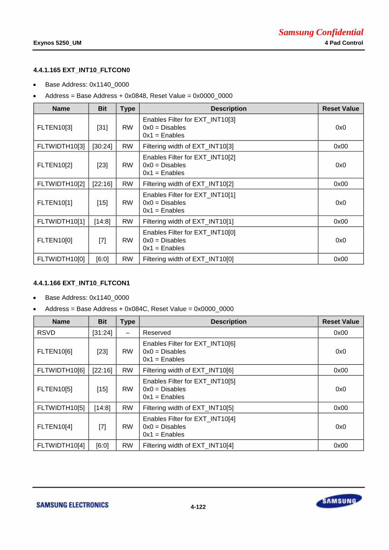
Samsung Confidential Exynos 5250_UM 4 Pad Control
4-122
4.4.1.165 EXT_INT10_FLTCON0
Base Address: 0x1140_0000
Address = Base Address + 0x0848, Reset Value = 0x0000_0000
Name Bit Type Description Reset Value
FLTEN10[3] [31] RW
Enables Filter for EXT_INT10[3]
0x0 = Disables
0x1 = Enables
0x0
FLTWIDTH10[3] [30:24] RW Filtering width of EXT_INT10[3] 0x00
FLTEN10[2] [23] RW
Enables Filter for EXT_INT10[2]
0x0 = Disables
0x1 = Enables
0x0
FLTWIDTH10[2] [22:16] RW Filtering width of EXT_INT10[2] 0x00
FLTEN10[1] [15] RW
Enables Filter for EXT_INT10[1]
0x0 = Disables
0x1 = Enables
0x0
FLTWIDTH10[1] [14:8] RW Filtering width of EXT_INT10[1] 0x00
FLTEN10[0] [7] RW
Enables Filter for EXT_INT10[0]
0x0 = Disables
0x1 = Enables
0x0
FLTWIDTH10[0] [6:0] RW Filtering width of EXT_INT10[0] 0x00
4.4.1.166 EXT_INT10_FLTCON1
Base Address: 0x1140_0000
Address = Base Address + 0x084C, Reset Value = 0x0000_0000
Name Bit Type Description Reset Value
RSVD [31:24] – Reserved 0x00
FLTEN10[6] [23] RW
Enables Filter for EXT_INT10[6]
0x0 = Disables
0x1 = Enables
0x0
FLTWIDTH10[6] [22:16] RW Filtering width of EXT_INT10[6] 0x00
FLTEN10[5] [15] RW
Enables Filter for EXT_INT10[5]
0x0 = Disables
0x1 = Enables
0x0
FLTWIDTH10[5] [14:8] RW Filtering width of EXT_INT10[5] 0x00
FLTEN10[4] [7] RW
Enables Filter for EXT_INT10[4]
0x0 = Disables
0x1 = Enables
0x0
FLTWIDTH10[4] [6:0] RW Filtering width of EXT_INT10[4] 0x00
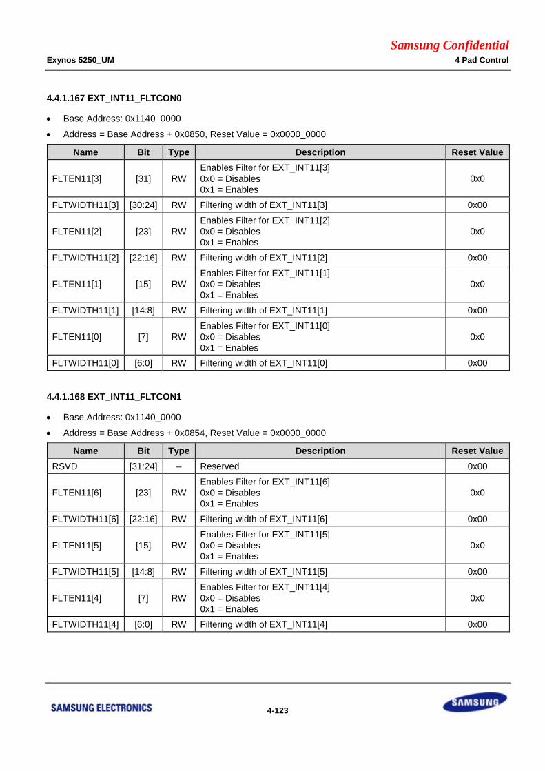
Samsung Confidential Exynos 5250_UM 4 Pad Control
4-123
4.4.1.167 EXT_INT11_FLTCON0
Base Address: 0x1140_0000
Address = Base Address + 0x0850, Reset Value = 0x0000_0000
Name Bit Type Description Reset Value
FLTEN11[3] [31] RW
Enables Filter for EXT_INT11[3]
0x0 = Disables
0x1 = Enables
0x0
FLTWIDTH11[3] [30:24] RW Filtering width of EXT_INT11[3] 0x00
FLTEN11[2] [23] RW
Enables Filter for EXT_INT11[2]
0x0 = Disables
0x1 = Enables
0x0
FLTWIDTH11[2] [22:16] RW Filtering width of EXT_INT11[2] 0x00
FLTEN11[1] [15] RW
Enables Filter for EXT_INT11[1]
0x0 = Disables
0x1 = Enables
0x0
FLTWIDTH11[1] [14:8] RW Filtering width of EXT_INT11[1] 0x00
FLTEN11[0] [7] RW
Enables Filter for EXT_INT11[0]
0x0 = Disables
0x1 = Enables
0x0
FLTWIDTH11[0] [6:0] RW Filtering width of EXT_INT11[0] 0x00
4.4.1.168 EXT_INT11_FLTCON1
Base Address: 0x1140_0000
Address = Base Address + 0x0854, Reset Value = 0x0000_0000
Name Bit Type Description Reset Value
RSVD [31:24] – Reserved 0x00
FLTEN11[6] [23] RW
Enables Filter for EXT_INT11[6]
0x0 = Disables
0x1 = Enables
0x0
FLTWIDTH11[6] [22:16] RW Filtering width of EXT_INT11[6] 0x00
FLTEN11[5] [15] RW
Enables Filter for EXT_INT11[5]
0x0 = Disables
0x1 = Enables
0x0
FLTWIDTH11[5] [14:8] RW Filtering width of EXT_INT11[5] 0x00
FLTEN11[4] [7] RW
Enables Filter for EXT_INT11[4]
0x0 = Disables
0x1 = Enables
0x0
FLTWIDTH11[4] [6:0] RW Filtering width of EXT_INT11[4] 0x00
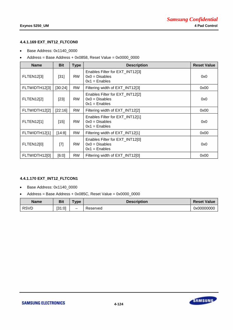
Samsung Confidential Exynos 5250_UM 4 Pad Control
4-124
4.4.1.169 EXT_INT12_FLTCON0
Base Address: 0x1140_0000
Address = Base Address + 0x0858, Reset Value = 0x0000_0000
Name Bit Type Description Reset Value
FLTEN12[3] [31] RW
Enables Filter for EXT_INT12[3]
0x0 = Disables
0x1 = Enables
0x0
FLTWIDTH12[3] [30:24] RW Filtering width of EXT_INT12[3] 0x00
FLTEN12[2] [23] RW
Enables Filter for EXT_INT12[2]
0x0 = Disables
0x1 = Enables
0x0
FLTWIDTH12[2] [22:16] RW Filtering width of EXT_INT12[2] 0x00
FLTEN12[1] [15] RW
Enables Filter for EXT_INT12[1]
0x0 = Disables
0x1 = Enables
0x0
FLTWIDTH12[1] [14:8] RW Filtering width of EXT_INT12[1] 0x00
FLTEN12[0] [7] RW
Enables Filter for EXT_INT12[0]
0x0 = Disables
0x1 = Enables
0x0
FLTWIDTH12[0] [6:0] RW Filtering width of EXT_INT12[0] 0x00
4.4.1.170 EXT_INT12_FLTCON1
Base Address: 0x1140_0000
Address = Base Address + 0x085C, Reset Value = 0x0000_0000
Name Bit Type Description Reset Value
RSVD [31:0] – Reserved 0x00000000

Samsung Confidential Exynos 5250_UM 4 Pad Control
4-125
4.4.1.171 EXT_INT13_FLTCON0
Base Address: 0x1140_0000
Address = Base Address + 0x0860, Reset Value = 0x0000_0000
Name Bit Type Description Reset Value
FLTEN13[3] [31] RW
Enables Filter for EXT_INT13[3]
0x0 = Disables
0x1 = Enables
0x0
FLTWIDTH13[3] [30:24] RW Filtering width of EXT_INT13[3] 0x00
FLTEN13[2] [23] RW
Enables Filter for EXT_INT13[2]
0x0 = Disables
0x1 = Enables
0x0
FLTWIDTH13[2] [22:16] RW Filtering width of EXT_INT13[2] 0x00
FLTEN13[1] [15] RW
Enables Filter for EXT_INT13[1]
0x0 = Disables
0x1 = Enables
0x0
FLTWIDTH13[1] [14:8] RW Filtering width of EXT_INT13[1] 0x00
FLTEN13[0] [7] RW
Enables Filter for EXT_INT13[0]
0x0 = Disables
0x1 = Enables
0x0
FLTWIDTH13[0] [6:0] RW Filtering width of EXT_INT13[0] 0x00

Samsung Confidential Exynos 5250_UM 4 Pad Control
4-126
4.4.1.172 EXT_INT13_FLTCON1
Base Address: 0x1140_0000
Address = Base Address + 0x0864, Reset Value = 0x0000_0000
Name Bit Type Description Reset Value
FLTEN13[7] [31] RW
Enables Filter for EXT_INT13[7]
0x0 = Disables
0x1 = Enables
0x0
FLTWIDTH13[7] [30:24] RW Filtering width of EXT_INT13[7] 0x00
FLTEN13[6] [23] RW
Enables Filter for EXT_INT13[6]
0x0 = Disables
0x1 = Enables
0x0
FLTWIDTH13[6] [22:16] RW Filtering width of EXT_INT13[6] 0x00
FLTEN13[5] [15] RW
Enables Filter for EXT_INT13[5]
0x0 = Disables
0x1 = Enables
0x0
FLTWIDTH13[5] [14:8] RW Filtering width of EXT_INT13[5] 0x00
FLTEN13[4] [7] RW
Enables Filter for EXT_INT13[4]
0x0 = Disables
0x1 = Enables
0x0
FLTWIDTH13[4] [6:0] RW Filtering width of EXT_INT13[4] 0x00
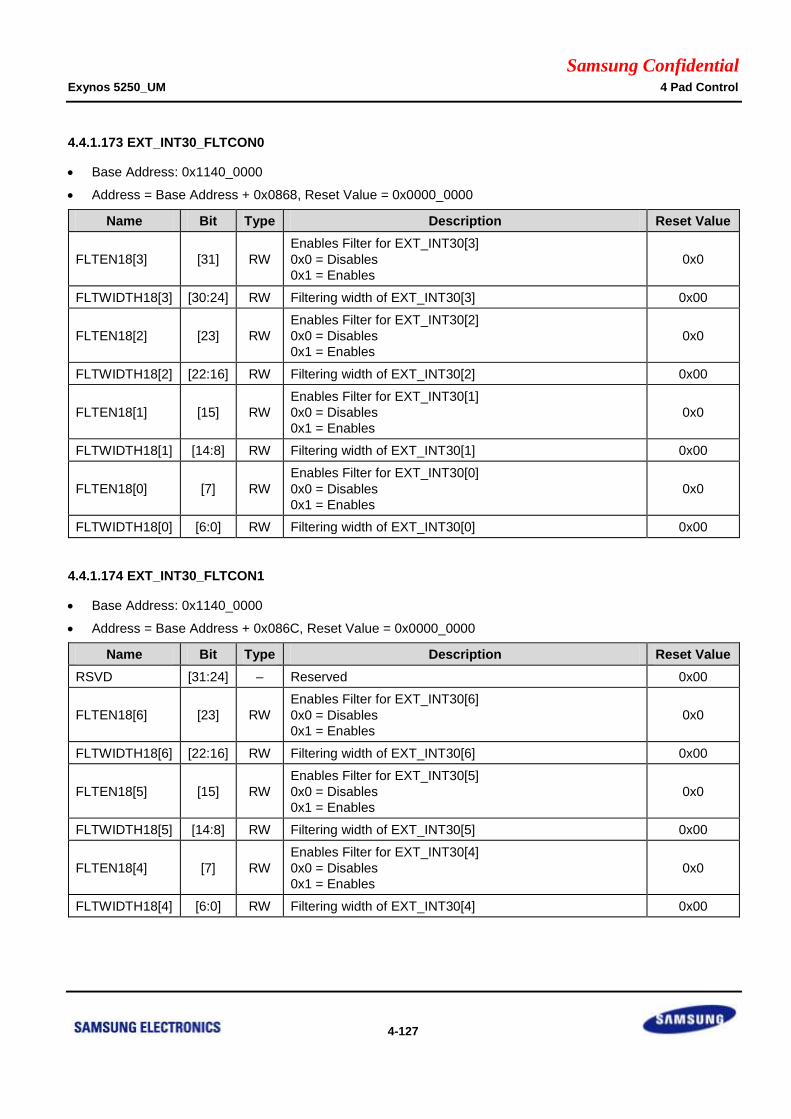
Samsung Confidential Exynos 5250_UM 4 Pad Control
4-127
4.4.1.173 EXT_INT30_FLTCON0
Base Address: 0x1140_0000
Address = Base Address + 0x0868, Reset Value = 0x0000_0000
Name Bit Type Description Reset Value
FLTEN18[3] [31] RW
Enables Filter for EXT_INT30[3]
0x0 = Disables
0x1 = Enables
0x0
FLTWIDTH18[3] [30:24] RW Filtering width of EXT_INT30[3] 0x00
FLTEN18[2] [23] RW
Enables Filter for EXT_INT30[2]
0x0 = Disables
0x1 = Enables
0x0
FLTWIDTH18[2] [22:16] RW Filtering width of EXT_INT30[2] 0x00
FLTEN18[1] [15] RW
Enables Filter for EXT_INT30[1]
0x0 = Disables
0x1 = Enables
0x0
FLTWIDTH18[1] [14:8] RW Filtering width of EXT_INT30[1] 0x00
FLTEN18[0] [7] RW
Enables Filter for EXT_INT30[0]
0x0 = Disables
0x1 = Enables
0x0
FLTWIDTH18[0] [6:0] RW Filtering width of EXT_INT30[0] 0x00
4.4.1.174 EXT_INT30_FLTCON1
Base Address: 0x1140_0000
Address = Base Address + 0x086C, Reset Value = 0x0000_0000
Name Bit Type Description Reset Value
RSVD [31:24] – Reserved 0x00
FLTEN18[6] [23] RW
Enables Filter for EXT_INT30[6]
0x0 = Disables
0x1 = Enables
0x0
FLTWIDTH18[6] [22:16] RW Filtering width of EXT_INT30[6] 0x00
FLTEN18[5] [15] RW
Enables Filter for EXT_INT30[5]
0x0 = Disables
0x1 = Enables
0x0
FLTWIDTH18[5] [14:8] RW Filtering width of EXT_INT30[5] 0x00
FLTEN18[4] [7] RW
Enables Filter for EXT_INT30[4]
0x0 = Disables
0x1 = Enables
0x0
FLTWIDTH18[4] [6:0] RW Filtering width of EXT_INT30[4] 0x00

Samsung Confidential Exynos 5250_UM 4 Pad Control
4-128
4.4.1.175 EXT_INT1_MASK
Base Address: 0x1140_0000
Address = Base Address + 0x0900, Reset Value = 0x0000_00FF
Name Bit Type Description Reset Value
RSVD [31:8] – Reserved 0x000000
EXT_INT1
_MASK[7] [7] RW
0x0 = Enables Interrupt
0x1 = Masks Interrupt 0x1
EXT_INT1
_MASK[6] [6] RW
0x0 = Enables Interrupt
0x1 = Masks Interrupt 0x1
EXT_INT1
_MASK[5] [5] RW
0x0 = Enables Interrupt
0x1 = Masks Interrupt 0x1
EXT_INT1
_MASK[4] [4] RW
0x0 = Enable Interrupt
0x1 = Masks Interrupt 0x1
EXT_INT1
_MASK[3] [3] RW
0x0 = Enables Interrupt
0x1 = Masks Interrupt 0x1
EXT_INT1
_MASK[2] [2] RW
0x0 = Enables Interrupt
0x1 = Masks Interrupt 0x1
EXT_INT1
_MASK[1] [1] RW
0x0 = Enables Interrupt
0x1 = Masks Interrupt 0x1
EXT_INT1
_MASK[0] [0] RW
0x0 = Enables Interrupt
0x1 = Masks Interrupt 0x1
4.4.1.176 EXT_INT2_MASK
Base Address: 0x1140_0000
Address = Base Address + 0x0904, Reset Value = 0x0000_003F
Name Bit Type Description Reset Value
RSVD [31:6] – Reserved 0x0000000
EXT_INT2
_MASK[5] [5] RW
0x0 = Enables Interrupt
0x1 = Masks Interrupt 0x1
EXT_INT2
_MASK[4] [4] RW
0x0 = Enables Interrupt
0x1 = Masks Interrupt 0x1
EXT_INT2
_MASK[3] [3] RW
0x0 = Enables Interrupt
0x1 = Masks Interrupt 0x1
EXT_INT2
_MASK[2] [2] RW
0x0 = Enables Interrupt
0x1 = Masks Interrupt 0x1
EXT_INT2
_MASK[1] [1] RW
0x0 = Enables Interrupt
0x1 = Masks Interrupt 0x1
EXT_INT2
_MASK[0] [0] RW
0x0 = Enables Interrupt
0x1 = Masks Interrupt 0x1
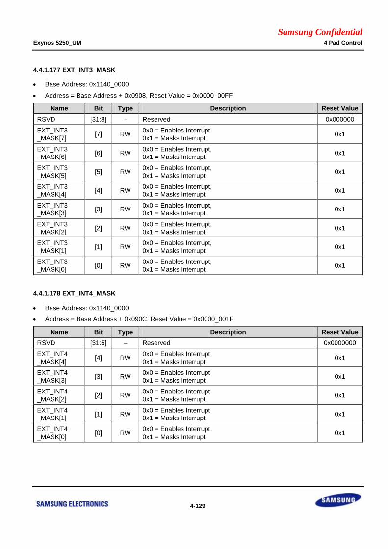
Samsung Confidential Exynos 5250_UM 4 Pad Control
4-129
4.4.1.177 EXT_INT3_MASK
Base Address: 0x1140_0000
Address = Base Address + 0x0908, Reset Value = 0x0000_00FF
Name Bit Type Description Reset Value
RSVD [31:8] – Reserved 0x000000
EXT_INT3
_MASK[7] [7] RW
0x0 = Enables Interrupt
0x1 = Masks Interrupt 0x1
EXT_INT3
_MASK[6] [6] RW
0x0 = Enables Interrupt,
0x1 = Masks Interrupt 0x1
EXT_INT3
_MASK[5] [5] RW
0x0 = Enables Interrupt,
0x1 = Masks Interrupt 0x1
EXT_INT3
_MASK[4] [4] RW
0x0 = Enables Interrupt,
0x1 = Masks Interrupt 0x1
EXT_INT3
_MASK[3] [3] RW
0x0 = Enables Interrupt,
0x1 = Masks Interrupt 0x1
EXT_INT3
_MASK[2] [2] RW
0x0 = Enables Interrupt,
0x1 = Masks Interrupt 0x1
EXT_INT3
_MASK[1] [1] RW
0x0 = Enables Interrupt,
0x1 = Masks Interrupt 0x1
EXT_INT3
_MASK[0] [0] RW
0x0 = Enables Interrupt,
0x1 = Masks Interrupt 0x1
4.4.1.178 EXT_INT4_MASK
Base Address: 0x1140_0000
Address = Base Address + 0x090C, Reset Value = 0x0000_001F
Name Bit Type Description Reset Value
RSVD [31:5] – Reserved 0x0000000
EXT_INT4
_MASK[4] [4] RW
0x0 = Enables Interrupt
0x1 = Masks Interrupt 0x1
EXT_INT4
_MASK[3] [3] RW
0x0 = Enables Interrupt
0x1 = Masks Interrupt 0x1
EXT_INT4
_MASK[2] [2] RW
0x0 = Enables Interrupt
0x1 = Masks Interrupt 0x1
EXT_INT4
_MASK[1] [1] RW
0x0 = Enables Interrupt
0x1 = Masks Interrupt 0x1
EXT_INT4
_MASK[0] [0] RW
0x0 = Enables Interrupt
0x1 = Masks Interrupt 0x1
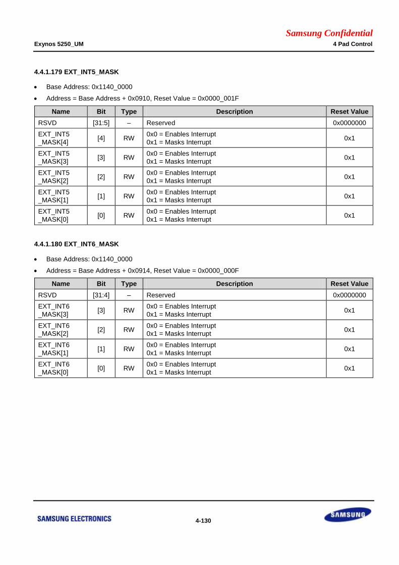
Samsung Confidential Exynos 5250_UM 4 Pad Control
4-130
4.4.1.179 EXT_INT5_MASK
Base Address: 0x1140_0000
Address = Base Address + 0x0910, Reset Value = 0x0000_001F
Name Bit Type Description Reset Value
RSVD [31:5] – Reserved 0x0000000
EXT_INT5
_MASK[4] [4] RW
0x0 = Enables Interrupt
0x1 = Masks Interrupt 0x1
EXT_INT5
_MASK[3] [3] RW
0x0 = Enables Interrupt
0x1 = Masks Interrupt 0x1
EXT_INT5
_MASK[2] [2] RW
0x0 = Enables Interrupt
0x1 = Masks Interrupt 0x1
EXT_INT5
_MASK[1] [1] RW
0x0 = Enables Interrupt
0x1 = Masks Interrupt 0x1
EXT_INT5
_MASK[0] [0] RW
0x0 = Enables Interrupt
0x1 = Masks Interrupt 0x1
4.4.1.180 EXT_INT6_MASK
Base Address: 0x1140_0000
Address = Base Address + 0x0914, Reset Value = 0x0000_000F
Name Bit Type Description Reset Value
RSVD [31:4] – Reserved 0x0000000
EXT_INT6
_MASK[3] [3] RW
0x0 = Enables Interrupt
0x1 = Masks Interrupt 0x1
EXT_INT6
_MASK[2] [2] RW
0x0 = Enables Interrupt
0x1 = Masks Interrupt 0x1
EXT_INT6
_MASK[1] [1] RW
0x0 = Enables Interrupt
0x1 = Masks Interrupt 0x1
EXT_INT6
_MASK[0] [0] RW
0x0 = Enables Interrupt
0x1 = Masks Interrupt 0x1
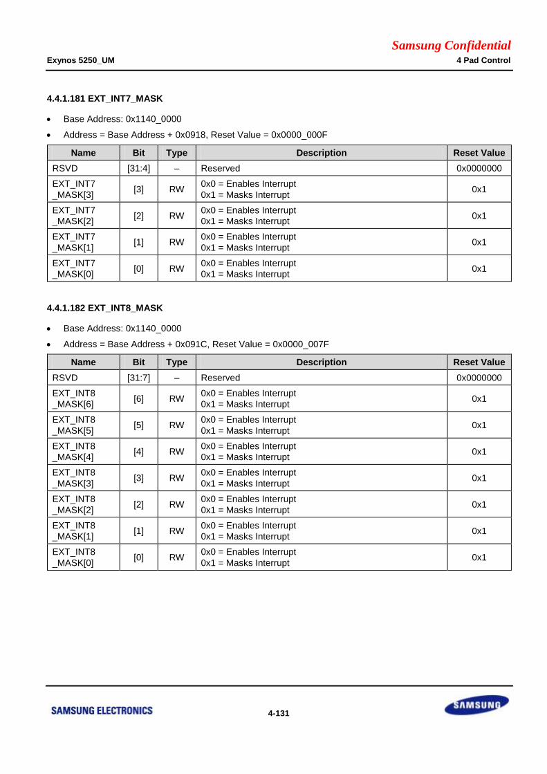
Samsung Confidential Exynos 5250_UM 4 Pad Control
4-131
4.4.1.181 EXT_INT7_MASK
Base Address: 0x1140_0000
Address = Base Address + 0x0918, Reset Value = 0x0000_000F
Name Bit Type Description Reset Value
RSVD [31:4] – Reserved 0x0000000
EXT_INT7
_MASK[3] [3] RW
0x0 = Enables Interrupt
0x1 = Masks Interrupt 0x1
EXT_INT7
_MASK[2] [2] RW
0x0 = Enables Interrupt
0x1 = Masks Interrupt 0x1
EXT_INT7
_MASK[1] [1] RW
0x0 = Enables Interrupt
0x1 = Masks Interrupt 0x1
EXT_INT7
_MASK[0] [0] RW
0x0 = Enables Interrupt
0x1 = Masks Interrupt 0x1
4.4.1.182 EXT_INT8_MASK
Base Address: 0x1140_0000
Address = Base Address + 0x091C, Reset Value = 0x0000_007F
Name Bit Type Description Reset Value
RSVD [31:7] – Reserved 0x0000000
EXT_INT8
_MASK[6] [6] RW
0x0 = Enables Interrupt
0x1 = Masks Interrupt 0x1
EXT_INT8
_MASK[5] [5] RW
0x0 = Enables Interrupt
0x1 = Masks Interrupt 0x1
EXT_INT8
_MASK[4] [4] RW
0x0 = Enables Interrupt
0x1 = Masks Interrupt 0x1
EXT_INT8
_MASK[3] [3] RW
0x0 = Enables Interrupt
0x1 = Masks Interrupt 0x1
EXT_INT8
_MASK[2] [2] RW
0x0 = Enables Interrupt
0x1 = Masks Interrupt 0x1
EXT_INT8
_MASK[1] [1] RW
0x0 = Enables Interrupt
0x1 = Masks Interrupt 0x1
EXT_INT8
_MASK[0] [0] RW
0x0 = Enables Interrupt
0x1 = Masks Interrupt 0x1
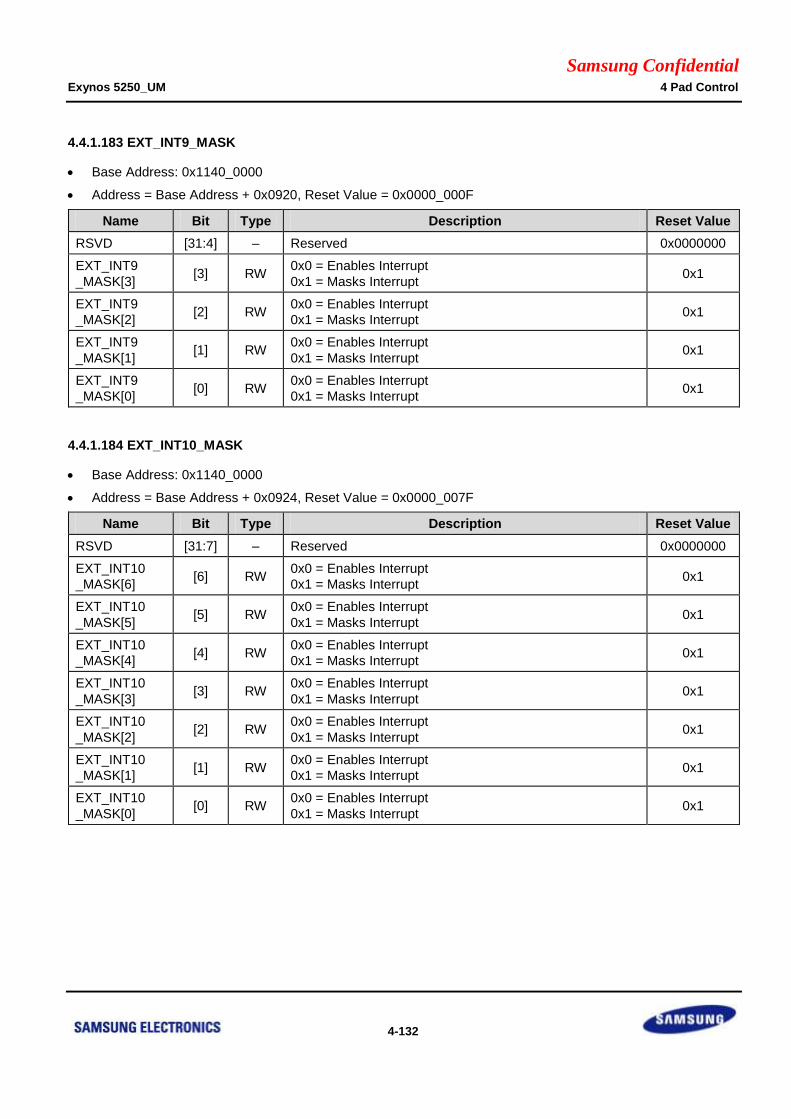
Samsung Confidential Exynos 5250_UM 4 Pad Control
4-132
4.4.1.183 EXT_INT9_MASK
Base Address: 0x1140_0000
Address = Base Address + 0x0920, Reset Value = 0x0000_000F
Name Bit Type Description Reset Value
RSVD [31:4] – Reserved 0x0000000
EXT_INT9
_MASK[3] [3] RW
0x0 = Enables Interrupt
0x1 = Masks Interrupt 0x1
EXT_INT9
_MASK[2] [2] RW
0x0 = Enables Interrupt
0x1 = Masks Interrupt 0x1
EXT_INT9
_MASK[1] [1] RW
0x0 = Enables Interrupt
0x1 = Masks Interrupt 0x1
EXT_INT9
_MASK[0] [0] RW
0x0 = Enables Interrupt
0x1 = Masks Interrupt 0x1
4.4.1.184 EXT_INT10_MASK
Base Address: 0x1140_0000
Address = Base Address + 0x0924, Reset Value = 0x0000_007F
Name Bit Type Description Reset Value
RSVD [31:7] – Reserved 0x0000000
EXT_INT10
_MASK[6] [6] RW
0x0 = Enables Interrupt
0x1 = Masks Interrupt 0x1
EXT_INT10
_MASK[5] [5] RW
0x0 = Enables Interrupt
0x1 = Masks Interrupt 0x1
EXT_INT10
_MASK[4] [4] RW
0x0 = Enables Interrupt
0x1 = Masks Interrupt 0x1
EXT_INT10
_MASK[3] [3] RW
0x0 = Enables Interrupt
0x1 = Masks Interrupt 0x1
EXT_INT10
_MASK[2] [2] RW
0x0 = Enables Interrupt
0x1 = Masks Interrupt 0x1
EXT_INT10
_MASK[1] [1] RW
0x0 = Enables Interrupt
0x1 = Masks Interrupt 0x1
EXT_INT10
_MASK[0] [0] RW
0x0 = Enables Interrupt
0x1 = Masks Interrupt 0x1

Samsung Confidential Exynos 5250_UM 4 Pad Control
4-133
4.4.1.185 EXT_INT11_MASK
Base Address: 0x1140_0000
Address = Base Address + 0x0928, Reset Value = 0x0000_007F
Name Bit Type Description Reset Value
RSVD [31:7] – Reserved 0x0000000
EXT_INT11
_MASK[6] [6] RW
0x0 = Enables Interrupt
0x1 = Masks Interrupt 0x1
EXT_INT11
_MASK[5] [5] RW
0x0 = Enables Interrupt
0x1 = Masks Interrupt 0x1
EXT_INT11
_MASK[4] [4] RW
0x0 = Enables Interrupt
0x1 = Masks Interrupt 0x1
EXT_INT11
_MASK[3] [3] RW
0x0 = Enables Interrupt
0x1 = Masks Interrupt 0x1
EXT_INT11
_MASK[2] [2] RW
0x0 = Enables Interrupt
0x1 = Masks Interrupt 0x1
EXT_INT11
_MASK[1] [1] RW
0x0 = Enables Interrupt
0x1 = Masks Interrupt 0x1
EXT_INT11
_MASK[0] [0] RW
0x0 = Enables Interrupt
0x1 = Masks Interrupt 0x1
4.4.1.186 EXT_INT12_MASK
Base Address: 0x1140_0000
Address = Base Address + 0x092C, Reset Value = 0x0000_000F
Name Bit Type Description Reset Value
RSVD [31:4] – Reserved 0x0000000
EXT_INT12
_MASK[3] [3] RW
0x0 = Enables Interrupt
0x1 = Masks Interrupt 0x1
EXT_INT12
_MASK[2] [2] RW
0x0 = Enables Interrupt
0x1 = Masks Interrupt 0x1
EXT_INT12
_MASK[1] [1] RW
0x0 = Enables Interrupt
0x1 = Masks Interrupt 0x1
EXT_INT12
_MASK[0] [0] RW
0x0 = Enables Interrupt
0x1 = Masks Interrupt 0x1

Samsung Confidential Exynos 5250_UM 4 Pad Control
4-134
4.4.1.187 EXT_INT13_MASK
Base Address: 0x1140_0000
Address = Base Address + 0x0930, Reset Value = 0x0000_00FF
Name Bit Type Description Reset Value
RSVD [31:8] – Reserved 0x000000
EXT_INT13
_MASK[7] [7] RW
0x0 = Enables Interrupt
0x1 = Masks Interrupt 0x1
EXT_INT13
_MASK[6] [6] RW
0x0 = Enables Interrupt
0x1 = Masks Interrupt 0x1
EXT_INT13
_MASK[5] [5] RW
0x0 = Enables Interrupt
0x1 = Masks Interrupt 0x1
EXT_INT13
_MASK[4] [4] RW
0x0 = Enables Interrupt
0x1 = Masks Interrupt 0x1
EXT_INT13
_MASK[3] [3] RW
0x0 = Enables Interrupt
0x1 = Masks Interrupt 0x1
EXT_INT13
_MASK[2] [2] RW
0x0 = Enables Interrupt
0x1 = Masks Interrupt 0x1
EXT_INT13
_MASK[1] [1] RW
0x0 = Enables Interrupt
0x1 = Masks Interrupt 0x1
EXT_INT13
_MASK[0] [0] RW
0x0 = Enables Interrupt
0x1 = Masks Interrupt 0x1
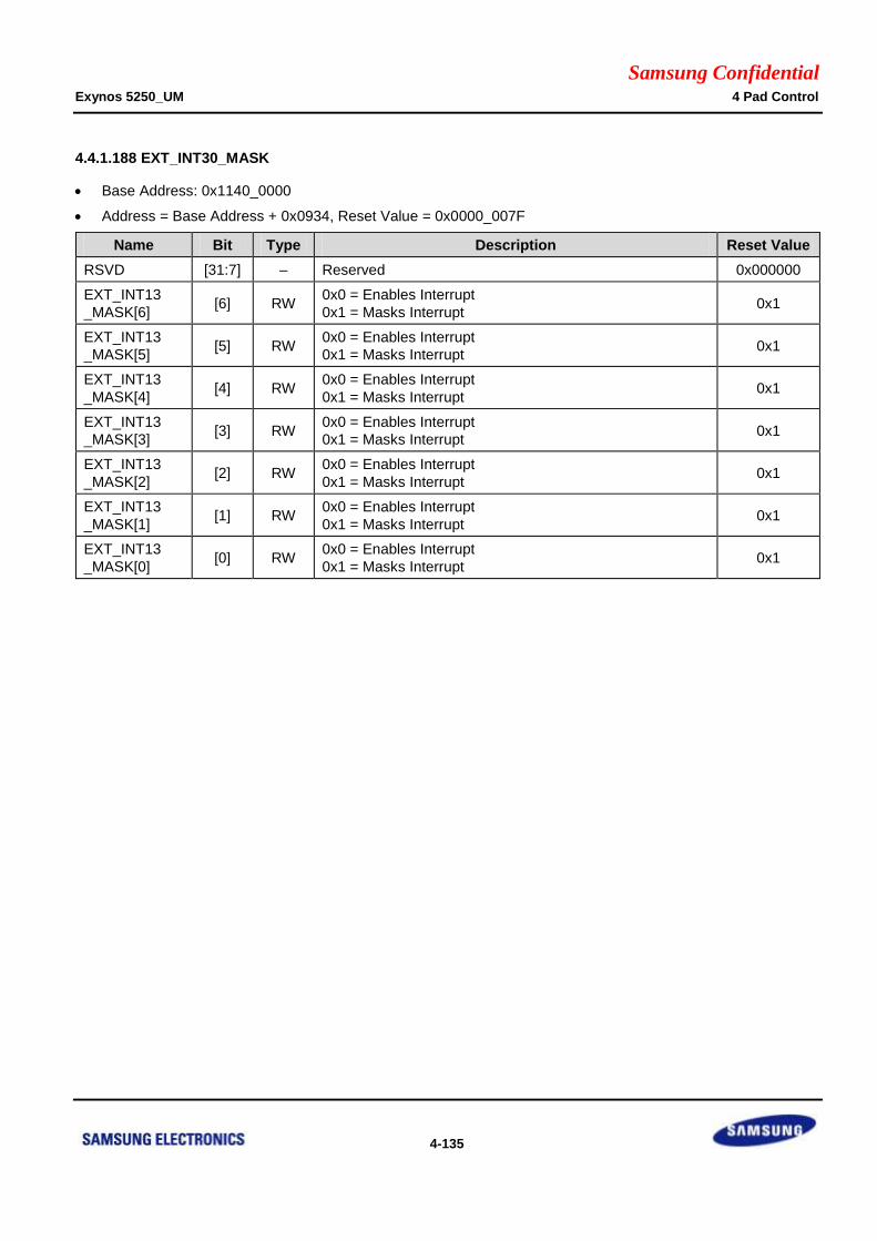
Samsung Confidential Exynos 5250_UM 4 Pad Control
4-135
4.4.1.188 EXT_INT30_MASK
Base Address: 0x1140_0000
Address = Base Address + 0x0934, Reset Value = 0x0000_007F
Name Bit Type Description Reset Value
RSVD [31:7] – Reserved 0x000000
EXT_INT13
_MASK[6] [6] RW
0x0 = Enables Interrupt
0x1 = Masks Interrupt 0x1
EXT_INT13
_MASK[5] [5] RW
0x0 = Enables Interrupt
0x1 = Masks Interrupt 0x1
EXT_INT13
_MASK[4] [4] RW
0x0 = Enables Interrupt
0x1 = Masks Interrupt 0x1
EXT_INT13
_MASK[3] [3] RW
0x0 = Enables Interrupt
0x1 = Masks Interrupt 0x1
EXT_INT13
_MASK[2] [2] RW
0x0 = Enables Interrupt
0x1 = Masks Interrupt 0x1
EXT_INT13
_MASK[1] [1] RW
0x0 = Enables Interrupt
0x1 = Masks Interrupt 0x1
EXT_INT13
_MASK[0] [0] RW
0x0 = Enables Interrupt
0x1 = Masks Interrupt 0x1
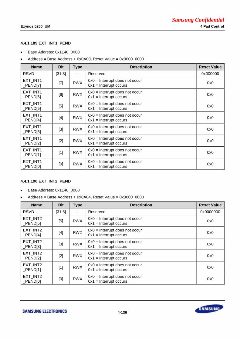
Samsung Confidential Exynos 5250_UM 4 Pad Control
4-136
4.4.1.189 EXT_INT1_PEND
Base Address: 0x1140_0000
Address = Base Address + 0x0A00, Reset Value = 0x0000_0000
Name Bit Type Description Reset Value
RSVD [31:8] – Reserved 0x000000
EXT_INT1
_PEND[7] [7] RWX
0x0 = Interrupt does not occur
0x1 = Interrupt occurs 0x0
EXT_INT1
_PEND[6] [6] RWX
0x0 = Interrupt does not occur
0x1 = Interrupt occurs 0x0
EXT_INT1
_PEND[5] [5] RWX
0x0 = Interrupt does not occur
0x1 = Interrupt occurs 0x0
EXT_INT1
_PEND[4] [4] RWX
0x0 = Interrupt does not occur
0x1 = Interrupt occurs 0x0
EXT_INT1
_PEND[3] [3] RWX
0x0 = Interrupt does not occur
0x1 = Interrupt occurs 0x0
EXT_INT1
_PEND[2] [2] RWX
0x0 = Interrupt does not occur
0x1 = Interrupt occurs 0x0
EXT_INT1
_PEND[1] [1] RWX
0x0 = Interrupt does not occur
0x1 = Interrupt occurs 0x0
EXT_INT1
_PEND[0] [0] RWX
0x0 = Interrupt does not occur
0x1 = Interrupt occurs 0x0
4.4.1.190 EXT_INT2_PEND
Base Address: 0x1140_0000
Address = Base Address + 0x0A04, Reset Value = 0x0000_0000
Name Bit Type Description Reset Value
RSVD [31:6] – Reserved 0x0000000
EXT_INT2
_PEND[5] [5] RWX
0x0 = Interrupt does not occur
0x1 = Interrupt occurs 0x0
EXT_INT2
_PEND[4] [4] RWX
0x0 = Interrupt does not occur
0x1 = Interrupt occurs 0x0
EXT_INT2
_PEND[3] [3] RWX
0x0 = Interrupt does not occur
0x1 = Interrupt occurs 0x0
EXT_INT2
_PEND[2] [2] RWX
0x0 = Interrupt does not occur
0x1 = Interrupt occurs 0x0
EXT_INT2
_PEND[1] [1] RWX
0x0 = Interrupt does not occur
0x1 = Interrupt occurs 0x0
EXT_INT2
_PEND[0] [0] RWX
0x0 = Interrupt does not occur
0x1 = Interrupt occurs 0x0
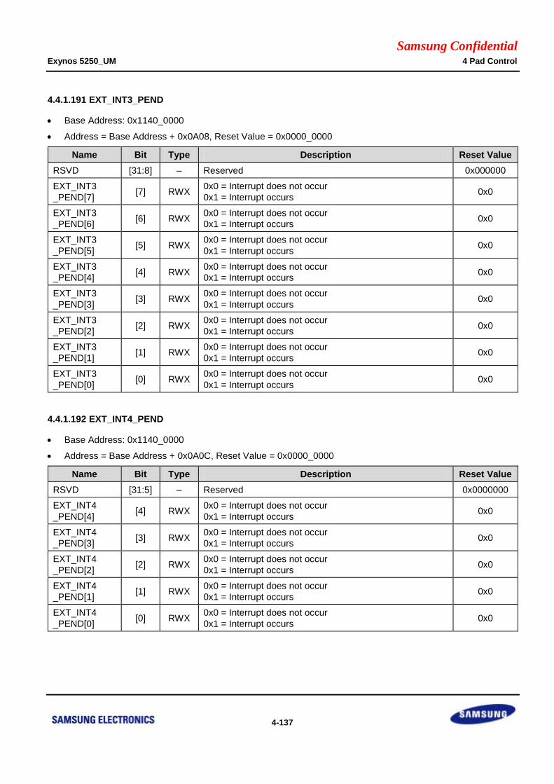
Samsung Confidential Exynos 5250_UM 4 Pad Control
4-137
4.4.1.191 EXT_INT3_PEND
Base Address: 0x1140_0000
Address = Base Address + 0x0A08, Reset Value = 0x0000_0000
Name Bit Type Description Reset Value
RSVD [31:8] – Reserved 0x000000
EXT_INT3
_PEND[7] [7] RWX
0x0 = Interrupt does not occur
0x1 = Interrupt occurs 0x0
EXT_INT3
_PEND[6] [6] RWX
0x0 = Interrupt does not occur
0x1 = Interrupt occurs 0x0
EXT_INT3
_PEND[5] [5] RWX
0x0 = Interrupt does not occur
0x1 = Interrupt occurs 0x0
EXT_INT3
_PEND[4] [4] RWX
0x0 = Interrupt does not occur
0x1 = Interrupt occurs 0x0
EXT_INT3
_PEND[3] [3] RWX
0x0 = Interrupt does not occur
0x1 = Interrupt occurs 0x0
EXT_INT3
_PEND[2] [2] RWX
0x0 = Interrupt does not occur
0x1 = Interrupt occurs 0x0
EXT_INT3
_PEND[1] [1] RWX
0x0 = Interrupt does not occur
0x1 = Interrupt occurs 0x0
EXT_INT3
_PEND[0] [0] RWX
0x0 = Interrupt does not occur
0x1 = Interrupt occurs 0x0
4.4.1.192 EXT_INT4_PEND
Base Address: 0x1140_0000
Address = Base Address + 0x0A0C, Reset Value = 0x0000_0000
Name Bit Type Description Reset Value
RSVD [31:5] – Reserved 0x0000000
EXT_INT4
_PEND[4] [4] RWX
0x0 = Interrupt does not occur
0x1 = Interrupt occurs 0x0
EXT_INT4
_PEND[3] [3] RWX
0x0 = Interrupt does not occur
0x1 = Interrupt occurs 0x0
EXT_INT4
_PEND[2] [2] RWX
0x0 = Interrupt does not occur
0x1 = Interrupt occurs 0x0
EXT_INT4
_PEND[1] [1] RWX
0x0 = Interrupt does not occur
0x1 = Interrupt occurs 0x0
EXT_INT4
_PEND[0] [0] RWX
0x0 = Interrupt does not occur
0x1 = Interrupt occurs 0x0
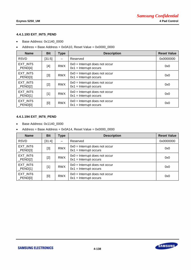
Samsung Confidential Exynos 5250_UM 4 Pad Control
4-138
4.4.1.193 EXT_INT5_PEND
Base Address: 0x1140_0000
Address = Base Address + 0x0A10, Reset Value = 0x0000_0000
Name Bit Type Description Reset Value
RSVD [31:5] – Reserved 0x0000000
EXT_INT5
_PEND[4] [4] RWX
0x0 = Interrupt does not occur
0x1 = Interrupt occurs 0x0
EXT_INT5
_PEND[3] [3] RWX
0x0 = Interrupt does not occur
0x1 = Interrupt occurs 0x0
EXT_INT5
_PEND[2] [2] RWX
0x0 = Interrupt does not occur
0x1 = Interrupt occurs 0x0
EXT_INT5
_PEND[1] [1] RWX
0x0 = Interrupt does not occur
0x1 = Interrupt occurs 0x0
EXT_INT5
_PEND[0] [0] RWX
0x0 = Interrupt does not occur
0x1 = Interrupt occurs 0x0
4.4.1.194 EXT_INT6_PEND
Base Address: 0x1140_0000
Address = Base Address + 0x0A14, Reset Value = 0x0000_0000
Name Bit Type Description Reset Value
RSVD [31:4] – Reserved 0x0000000
EXT_INT6
_PEND[3] [3] RWX
0x0 = Interrupt does not occur
0x1 = Interrupt occurs 0x0
EXT_INT6
_PEND[2] [2] RWX
0x0 = Interrupt does not occur
0x1 = Interrupt occurs 0x0
EXT_INT6
_PEND[1] [1] RWX
0x0 = Interrupt does not occur
0x1 = Interrupt occurs 0x0
EXT_INT6
_PEND[0] [0] RWX
0x0 = Interrupt does not occur
0x1 = Interrupt occurs 0x0

Samsung Confidential Exynos 5250_UM 4 Pad Control
4-139
4.4.1.195 EXT_INT7_PEND
Base Address: 0x1140_0000
Address = Base Address + 0x0A18, Reset Value = 0x0000_0000
Name Bit Type Description Reset Value
RSVD [31:4] – Reserved 0x0000000
EXT_INT7
_PEND[3] [3] RWX
0x0 = Interrupt does not occur
0x1 = Interrupt occurs 0x0
EXT_INT7
_PEND[2] [2] RWX
0x0 = Interrupt does not occur
0x1 = Interrupt occurs 0x0
EXT_INT7
_PEND[1] [1] RWX
0x0 = Interrupt does not occur
0x1 = Interrupt occurs 0x0
EXT_INT7
_PEND[0] [0] RWX
0x0 = Interrupt does not occur
0x1 = Interrupt occurs 0x0
4.4.1.196 EXT_INT8_PEND
Base Address: 0x1140_0000
Address = Base Address + 0x0A1C, Reset Value = 0x0000_0000
Name Bit Type Description Reset Value
RSVD [31:7] – Reserved 0x0000000
EXT_INT8
_PEND[6] [6] RWX
0x0 = Interrupt does not occur
0x1 = Interrupt occurs 0x0
EXT_INT8
_PEND[5] [5] RWX
0x0 = Interrupt does not occur
0x1 = Interrupt occurs 0x0
EXT_INT8
_PEND[4] [4] RWX
0x0 = Interrupt does not occur
0x1 = Interrupt occurs 0x0
EXT_INT8
_PEND[3] [3] RWX
0x0 = Interrupt does not occur
0x1 = Interrupt occurs 0x0
EXT_INT8
_PEND[2] [2] RWX
0x0 = Interrupt does not occur
0x1 = Interrupt occurs 0x0
EXT_INT8
_PEND[1] [1] RWX
0x0 = Interrupt does not occur
0x1 = Interrupt occurs 0x0
EXT_INT8
_PEND[0] [0] RWX
0x0 = Interrupt does not occur
0x1 = Interrupt occurs 0x0
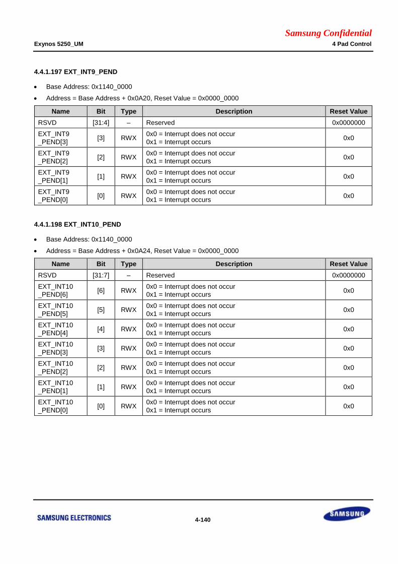
Samsung Confidential Exynos 5250_UM 4 Pad Control
4-140
4.4.1.197 EXT_INT9_PEND
Base Address: 0x1140_0000
Address = Base Address + 0x0A20, Reset Value = 0x0000_0000
Name Bit Type Description Reset Value
RSVD [31:4] – Reserved 0x0000000
EXT_INT9
_PEND[3] [3] RWX
0x0 = Interrupt does not occur
0x1 = Interrupt occurs 0x0
EXT_INT9
_PEND[2] [2] RWX
0x0 = Interrupt does not occur
0x1 = Interrupt occurs 0x0
EXT_INT9
_PEND[1] [1] RWX
0x0 = Interrupt does not occur
0x1 = Interrupt occurs 0x0
EXT_INT9
_PEND[0] [0] RWX
0x0 = Interrupt does not occur
0x1 = Interrupt occurs 0x0
4.4.1.198 EXT_INT10_PEND
Base Address: 0x1140_0000
Address = Base Address + 0x0A24, Reset Value = 0x0000_0000
Name Bit Type Description Reset Value
RSVD [31:7] – Reserved 0x0000000
EXT_INT10
_PEND[6] [6] RWX
0x0 = Interrupt does not occur
0x1 = Interrupt occurs 0x0
EXT_INT10
_PEND[5] [5] RWX
0x0 = Interrupt does not occur
0x1 = Interrupt occurs 0x0
EXT_INT10
_PEND[4] [4] RWX
0x0 = Interrupt does not occur
0x1 = Interrupt occurs 0x0
EXT_INT10
_PEND[3] [3] RWX
0x0 = Interrupt does not occur
0x1 = Interrupt occurs 0x0
EXT_INT10
_PEND[2] [2] RWX
0x0 = Interrupt does not occur
0x1 = Interrupt occurs 0x0
EXT_INT10
_PEND[1] [1] RWX
0x0 = Interrupt does not occur
0x1 = Interrupt occurs 0x0
EXT_INT10
_PEND[0] [0] RWX
0x0 = Interrupt does not occur
0x1 = Interrupt occurs 0x0
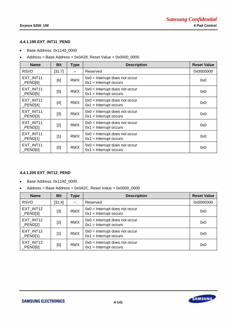
Samsung Confidential Exynos 5250_UM 4 Pad Control
4-141
4.4.1.199 EXT_INT11_PEND
Base Address: 0x1140_0000
Address = Base Address + 0x0A28, Reset Value = 0x0000_0000
Name Bit Type Description Reset Value
RSVD [31:7] – Reserved 0x0000000
EXT_INT11
_PEND[6] [6] RWX
0x0 = Interrupt does not occur
0x1 = Interrupt occurs 0x0
EXT_INT11
_PEND[5] [5] RWX
0x0 = Interrupt does not occur
0x1 = Interrupt occurs 0x0
EXT_INT11
_PEND[4] [4] RWX
0x0 = Interrupt does not occur
0x1 = Interrupt occurs 0x0
EXT_INT11
_PEND[3] [3] RWX
0x0 = Interrupt does not occur
0x1 = Interrupt occurs 0x0
EXT_INT11
_PEND[2] [2] RWX
0x0 = Interrupt does not occur
0x1 = Interrupt occurs 0x0
EXT_INT11
_PEND[1] [1] RWX
0x0 = Interrupt does not occur
0x1 = Interrupt occurs 0x0
EXT_INT11
_PEND[0] [0] RWX
0x0 = Interrupt does not occur
0x1 = Interrupt occurs 0x0
4.4.1.200 EXT_INT12_PEND
Base Address: 0x1140_0000
Address = Base Address + 0x0A2C, Reset Value = 0x0000_0000
Name Bit Type Description Reset Value
RSVD [31:4] – Reserved 0x0000000
EXT_INT12
_PEND[3] [3] RWX
0x0 = Interrupt does not occur
0x1 = Interrupt occurs 0x0
EXT_INT12
_PEND[2] [2] RWX
0x0 = Interrupt does not occur
0x1 = Interrupt occurs 0x0
EXT_INT12
_PEND[1] [1] RWX
0x0 = Interrupt does not occur
0x1 = Interrupt occurs 0x0
EXT_INT12
_PEND[0] [0] RWX
0x0 = Interrupt does not occur
0x1 = Interrupt occurs 0x0
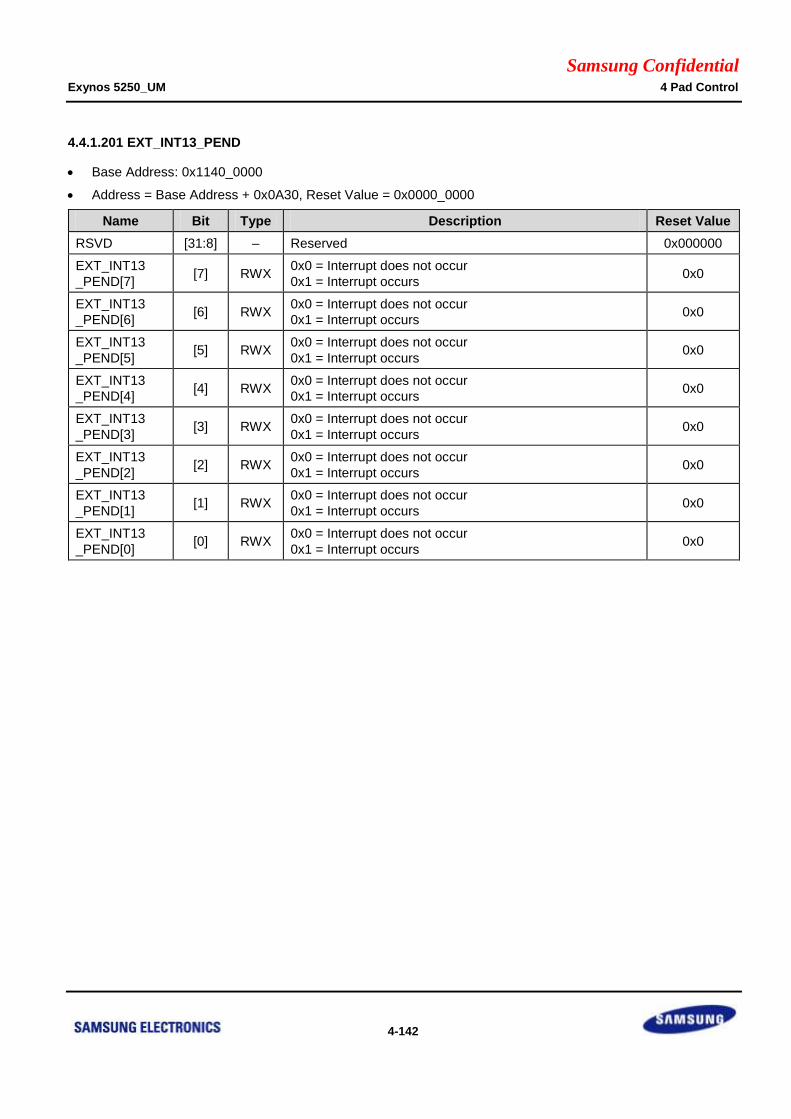
Samsung Confidential Exynos 5250_UM 4 Pad Control
4-142
4.4.1.201 EXT_INT13_PEND
Base Address: 0x1140_0000
Address = Base Address + 0x0A30, Reset Value = 0x0000_0000
Name Bit Type Description Reset Value
RSVD [31:8] – Reserved 0x000000
EXT_INT13
_PEND[7] [7] RWX
0x0 = Interrupt does not occur
0x1 = Interrupt occurs 0x0
EXT_INT13
_PEND[6] [6] RWX
0x0 = Interrupt does not occur
0x1 = Interrupt occurs 0x0
EXT_INT13
_PEND[5] [5] RWX
0x0 = Interrupt does not occur
0x1 = Interrupt occurs 0x0
EXT_INT13
_PEND[4] [4] RWX
0x0 = Interrupt does not occur
0x1 = Interrupt occurs 0x0
EXT_INT13
_PEND[3] [3] RWX
0x0 = Interrupt does not occur
0x1 = Interrupt occurs 0x0
EXT_INT13
_PEND[2] [2] RWX
0x0 = Interrupt does not occur
0x1 = Interrupt occurs 0x0
EXT_INT13
_PEND[1] [1] RWX
0x0 = Interrupt does not occur
0x1 = Interrupt occurs 0x0
EXT_INT13
_PEND[0] [0] RWX
0x0 = Interrupt does not occur
0x1 = Interrupt occurs 0x0
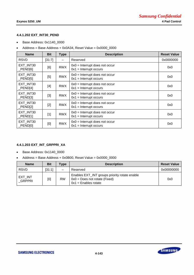
Samsung Confidential Exynos 5250_UM 4 Pad Control
4-143
4.4.1.202 EXT_INT30_PEND
Base Address: 0x1140_0000
Address = Base Address + 0x0A34, Reset Value = 0x0000_0000
Name Bit Type Description Reset Value
RSVD [31:7] – Reserved 0x0000000
EXT_INT30
_PEND[6] [6] RWX
0x0 = Interrupt does not occur
0x1 = Interrupt occurs 0x0
EXT_INT30
_PEND[5] [5] RWX
0x0 = Interrupt does not occur
0x1 = Interrupt occurs 0x0
EXT_INT30
_PEND[4] [4] RWX
0x0 = Interrupt does not occur
0x1 = Interrupt occurs 0x0
EXT_INT30
_PEND[3] [3] RWX
0x0 = Interrupt does not occur
0x1 = Interrupt occurs 0x0
EXT_INT30
_PEND[2] [2] RWX
0x0 = Interrupt does not occur
0x1 = Interrupt occurs 0x0
EXT_INT30
_PEND[1] [1] RWX
0x0 = Interrupt does not occur
0x1 = Interrupt occurs 0x0
EXT_INT30
_PEND[0] [0] RWX
0x0 = Interrupt does not occur
0x1 = Interrupt occurs 0x0
4.4.1.203 EXT_INT_GRPPRI_XA
Base Address: 0x1140_0000
Address = Base Address + 0x0B00, Reset Value = 0x0000_0000
Name Bit Type Description Reset Value
RSVD [31:1] – Reserved 0x00000000
EXT_INT
_GRPPRI [0] RW
Enables EXT_INT groups priority rotate enable
0x0 = Does not rotate (Fixed)
0x1 = Enables rotate
0x0
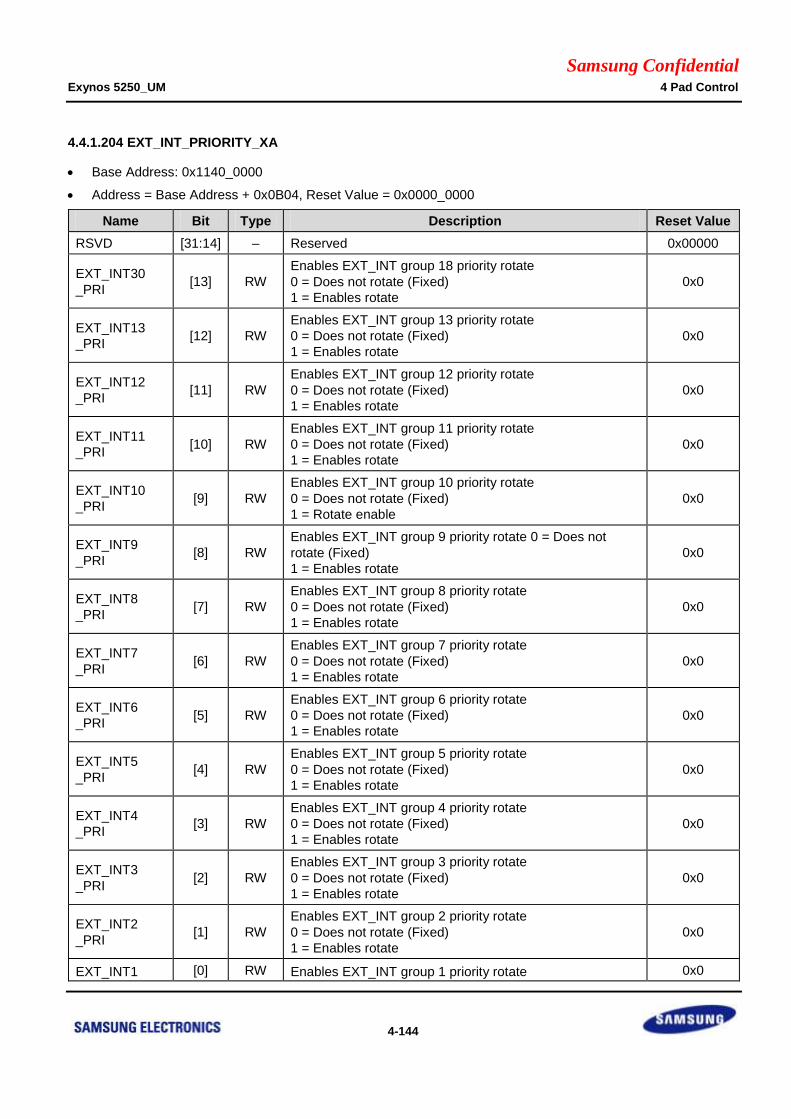
Samsung Confidential Exynos 5250_UM 4 Pad Control
4-144
4.4.1.204 EXT_INT_PRIORITY_XA
Base Address: 0x1140_0000
Address = Base Address + 0x0B04, Reset Value = 0x0000_0000
Name Bit Type Description Reset Value
RSVD [31:14] – Reserved 0x00000
EXT_INT30
_PRI [13] RW
Enables EXT_INT group 18 priority rotate
0 = Does not rotate (Fixed)
1 = Enables rotate
0x0
EXT_INT13
_PRI [12] RW
Enables EXT_INT group 13 priority rotate
0 = Does not rotate (Fixed)
1 = Enables rotate
0x0
EXT_INT12
_PRI [11] RW
Enables EXT_INT group 12 priority rotate
0 = Does not rotate (Fixed)
1 = Enables rotate
0x0
EXT_INT11
_PRI [10] RW
Enables EXT_INT group 11 priority rotate
0 = Does not rotate (Fixed)
1 = Enables rotate
0x0
EXT_INT10
_PRI [9] RW
Enables EXT_INT group 10 priority rotate
0 = Does not rotate (Fixed)
1 = Rotate enable
0x0
EXT_INT9
_PRI [8] RW
Enables EXT_INT group 9 priority rotate 0 = Does not
rotate (Fixed)
1 = Enables rotate
0x0
EXT_INT8
_PRI [7] RW
Enables EXT_INT group 8 priority rotate
0 = Does not rotate (Fixed)
1 = Enables rotate
0x0
EXT_INT7
_PRI [6] RW
Enables EXT_INT group 7 priority rotate
0 = Does not rotate (Fixed)
1 = Enables rotate
0x0
EXT_INT6
_PRI [5] RW
Enables EXT_INT group 6 priority rotate
0 = Does not rotate (Fixed)
1 = Enables rotate
0x0
EXT_INT5
_PRI [4] RW
Enables EXT_INT group 5 priority rotate
0 = Does not rotate (Fixed)
1 = Enables rotate
0x0
EXT_INT4
_PRI [3] RW
Enables EXT_INT group 4 priority rotate
0 = Does not rotate (Fixed)
1 = Enables rotate
0x0
EXT_INT3
_PRI [2] RW
Enables EXT_INT group 3 priority rotate
0 = Does not rotate (Fixed)
1 = Enables rotate
0x0
EXT_INT2
_PRI [1] RW
Enables EXT_INT group 2 priority rotate
0 = Does not rotate (Fixed)
1 = Enables rotate
0x0
EXT_INT1 [0] RW Enables EXT_INT group 1 priority rotate 0x0

Samsung Confidential Exynos 5250_UM 4 Pad Control
4-145
Name Bit Type Description Reset Value
_PRI 0 = Does not rotate (Fixed)
1 = Enables rotate
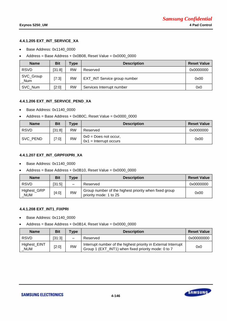
Samsung Confidential Exynos 5250_UM 4 Pad Control
4-146
4.4.1.205 EXT_INT_SERVICE_XA
Base Address: 0x1140_0000
Address = Base Address + 0x0B08, Reset Value = 0x0000_0000
Name Bit Type Description Reset Value
RSVD [31:8] RW Reserved 0x0000000
SVC_Group
_Num [7:3] RW EXT_INT Service group number 0x00
SVC_Num [2:0] RW Services Interrupt number 0x0
4.4.1.206 EXT_INT_SERVICE_PEND_XA
Base Address: 0x1140_0000
Address = Base Address + 0x0B0C, Reset Value = 0x0000_0000
Name Bit Type Description Reset Value
RSVD [31:8] RW Reserved 0x0000000
SVC_PEND [7:0] RW 0x0 = Does not occur,
0x1 = Interrupt occurs 0x00
4.4.1.207 EXT_INT_GRPFIXPRI_XA
Base Address: 0x1140_0000
Address = Base Address + 0x0B10, Reset Value = 0x0000_0000
Name Bit Type Description Reset Value
RSVD [31:5] – Reserved 0x0000000
Highest_GRP
_NUM [4:0] RW
Group number of the highest priority when fixed group
priority mode: 1 to 25 0x00
4.4.1.208 EXT_INT1_FIXPRI
Base Address: 0x1140_0000
Address = Base Address + 0x0B14, Reset Value = 0x0000_0000
Name Bit Type Description Reset Value
RSVD [31:3] – Reserved 0x00000000
Highest_EINT
_NUM [2:0] RW
Interrupt number of the highest priority in External Interrupt
Group 1 (EXT_INT1) when fixed priority mode: 0 to 7 0x0

Samsung Confidential Exynos 5250_UM 4 Pad Control
4-147
4.4.1.209 EXT_INT2_FIXPRI
Base Address: 0x1140_0000
Address = Base Address + 0x0B18, Reset Value = 0x0000_0000
Name Bit Type Description Reset Value
RSVD [31:3] – Reserved 0x00000000
Highest_EINT
_NUM [2:0] RW
Interrupt number of the highest priority in External Interrupt
Group 2 (EXT_INT2) when fixed priority mode: 0 to 7 0x0
4.4.1.210 EXT_INT3_FIXPRI
Base Address: 0x1140_0000
Address = Base Address + 0x0B1C, Reset Value = 0x0000_0000
Name Bit Type Description Reset Value
RSVD [31:3] – Reserved 0x00000000
Highest_EINT
_NUM [2:0] RW
Interrupt number of the highest priority in External Interrupt
Group 3 (EXT_INT3) when fixed priority mode: 0 to 7 0x0
4.4.1.211 EXT_INT4_FIXPRI
Base Address: 0x1140_0000
Address = Base Address + 0x0B20, Reset Value = 0x0000_0000
Name Bit Type Description Reset Value
RSVD [31:3] – Reserved 0x00000000
Highest_EINT
_NUM [2:0] RW
Interrupt number of the highest priority in External Interrupt
Group 4 (EXT_INT4) when fixed priority mode: 0 to 7 0x0
4.4.1.212 EXT_INT5_FIXPRI
Base Address: 0x1140_0000
Address = Base Address + 0x0B24, Reset Value = 0x0000_0000
Name Bit Type Description Reset Value
RSVD [31:3] – Reserved 0x00000000
Highest_EINT
_NUM [2:0] RW
Interrupt number of the highest priority in External Interrupt
Group 5 (EXT_INT5) when fixed priority mode: 0 to 7 0x0
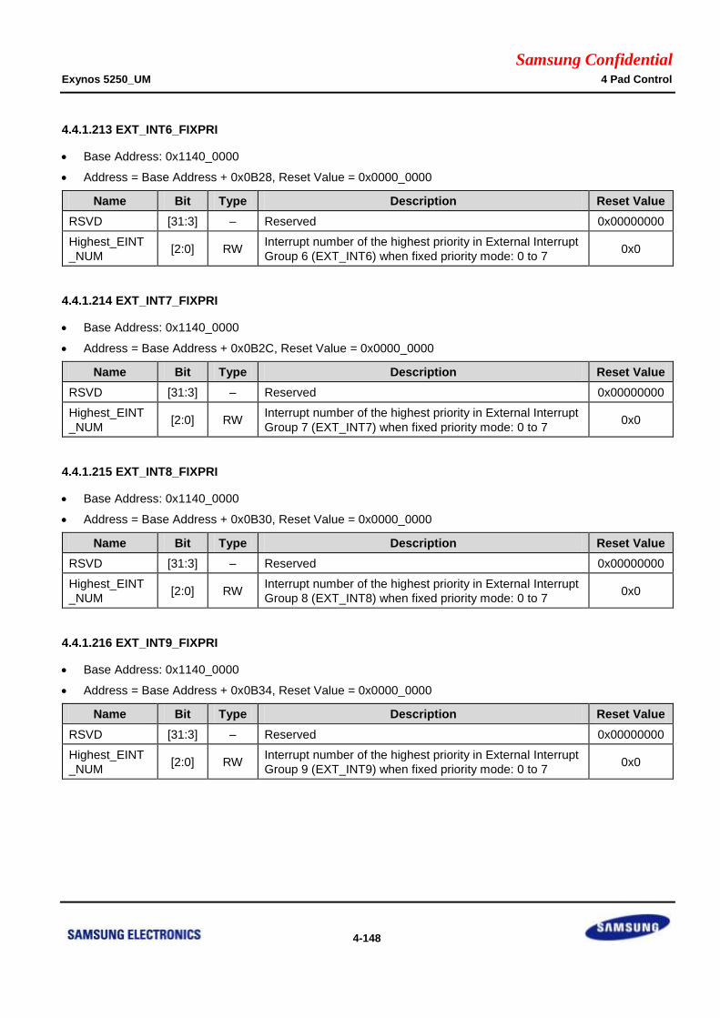
Samsung Confidential Exynos 5250_UM 4 Pad Control
4-148
4.4.1.213 EXT_INT6_FIXPRI
Base Address: 0x1140_0000
Address = Base Address + 0x0B28, Reset Value = 0x0000_0000
Name Bit Type Description Reset Value
RSVD [31:3] – Reserved 0x00000000
Highest_EINT
_NUM [2:0] RW
Interrupt number of the highest priority in External Interrupt
Group 6 (EXT_INT6) when fixed priority mode: 0 to 7 0x0
4.4.1.214 EXT_INT7_FIXPRI
Base Address: 0x1140_0000
Address = Base Address + 0x0B2C, Reset Value = 0x0000_0000
Name Bit Type Description Reset Value
RSVD [31:3] – Reserved 0x00000000
Highest_EINT
_NUM [2:0] RW
Interrupt number of the highest priority in External Interrupt
Group 7 (EXT_INT7) when fixed priority mode: 0 to 7 0x0
4.4.1.215 EXT_INT8_FIXPRI
Base Address: 0x1140_0000
Address = Base Address + 0x0B30, Reset Value = 0x0000_0000
Name Bit Type Description Reset Value
RSVD [31:3] – Reserved 0x00000000
Highest_EINT
_NUM [2:0] RW
Interrupt number of the highest priority in External Interrupt
Group 8 (EXT_INT8) when fixed priority mode: 0 to 7 0x0
4.4.1.216 EXT_INT9_FIXPRI
Base Address: 0x1140_0000
Address = Base Address + 0x0B34, Reset Value = 0x0000_0000
Name Bit Type Description Reset Value
RSVD [31:3] – Reserved 0x00000000
Highest_EINT
_NUM [2:0] RW
Interrupt number of the highest priority in External Interrupt
Group 9 (EXT_INT9) when fixed priority mode: 0 to 7 0x0
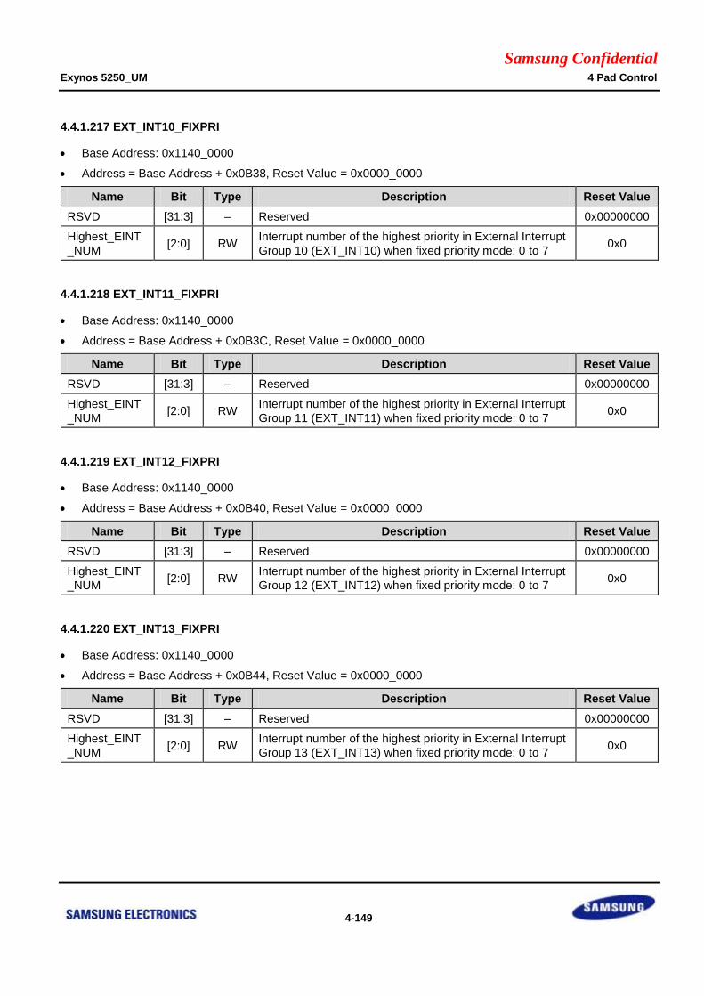
Samsung Confidential Exynos 5250_UM 4 Pad Control
4-149
4.4.1.217 EXT_INT10_FIXPRI
Base Address: 0x1140_0000
Address = Base Address + 0x0B38, Reset Value = 0x0000_0000
Name Bit Type Description Reset Value
RSVD [31:3] – Reserved 0x00000000
Highest_EINT
_NUM [2:0] RW
Interrupt number of the highest priority in External Interrupt
Group 10 (EXT_INT10) when fixed priority mode: 0 to 7 0x0
4.4.1.218 EXT_INT11_FIXPRI
Base Address: 0x1140_0000
Address = Base Address + 0x0B3C, Reset Value = 0x0000_0000
Name Bit Type Description Reset Value
RSVD [31:3] – Reserved 0x00000000
Highest_EINT
_NUM [2:0] RW
Interrupt number of the highest priority in External Interrupt
Group 11 (EXT_INT11) when fixed priority mode: 0 to 7 0x0
4.4.1.219 EXT_INT12_FIXPRI
Base Address: 0x1140_0000
Address = Base Address + 0x0B40, Reset Value = 0x0000_0000
Name Bit Type Description Reset Value
RSVD [31:3] – Reserved 0x00000000
Highest_EINT
_NUM [2:0] RW
Interrupt number of the highest priority in External Interrupt
Group 12 (EXT_INT12) when fixed priority mode: 0 to 7 0x0
4.4.1.220 EXT_INT13_FIXPRI
Base Address: 0x1140_0000
Address = Base Address + 0x0B44, Reset Value = 0x0000_0000
Name Bit Type Description Reset Value
RSVD [31:3] – Reserved 0x00000000
Highest_EINT
_NUM [2:0] RW
Interrupt number of the highest priority in External Interrupt
Group 13 (EXT_INT13) when fixed priority mode: 0 to 7 0x0
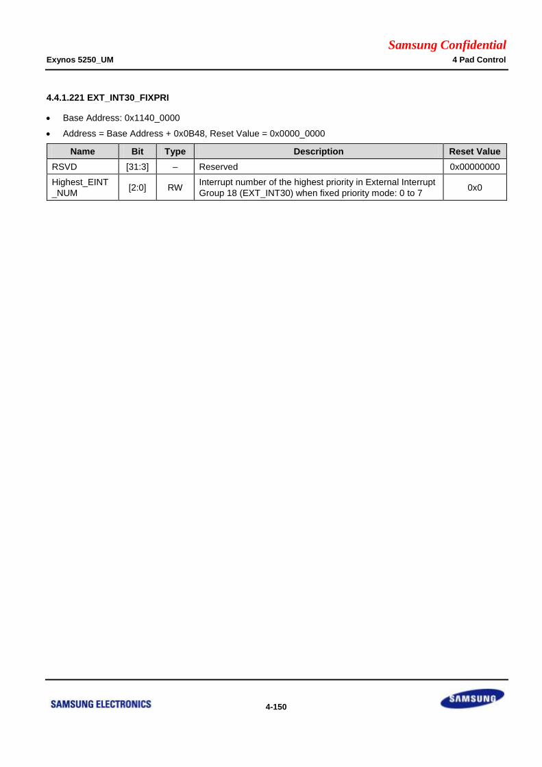
Samsung Confidential Exynos 5250_UM 4 Pad Control
4-150
4.4.1.221 EXT_INT30_FIXPRI
Base Address: 0x1140_0000
Address = Base Address + 0x0B48, Reset Value = 0x0000_0000
Name Bit Type Description Reset Value
RSVD [31:3] – Reserved 0x00000000
Highest_EINT
_NUM [2:0] RW
Interrupt number of the highest priority in External Interrupt
Group 18 (EXT_INT30) when fixed priority mode: 0 to 7 0x0
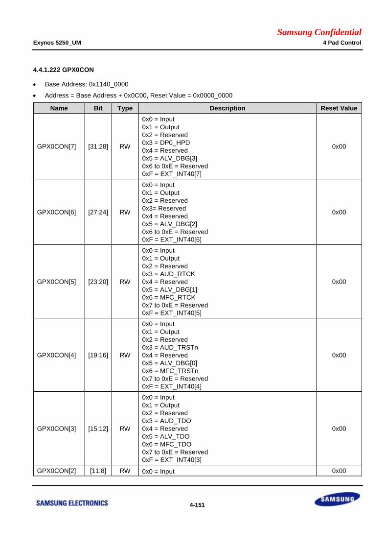
Samsung Confidential Exynos 5250_UM 4 Pad Control
4-151
4.4.1.222 GPX0CON
Base Address: 0x1140_0000
Address = Base Address + 0x0C00, Reset Value = 0x0000_0000
Name Bit Type Description Reset Value
GPX0CON[7] [31:28] RW
0x0 = Input
0x1 = Output
0x2 = Reserved
0x3 = DP0_HPD
0x4 = Reserved
0x5 = ALV_DBG[3]
0x6 to 0xE = Reserved
0xF = EXT_INT40[7]
0x00
GPX0CON[6] [27:24] RW
0x0 = Input
0x1 = Output
0x2 = Reserved
0x3= Reserved
0x4 = Reserved
0x5 = ALV_DBG[2]
0x6 to 0xE = Reserved
0xF = EXT_INT40[6]
0x00
GPX0CON[5] [23:20] RW
0x0 = Input
0x1 = Output
0x2 = Reserved
0x3 = AUD_RTCK
0x4 = Reserved
0x5 = ALV_DBG[1]
0x6 = MFC_RTCK
0x7 to 0xE = Reserved
0xF = EXT_INT40[5]
0x00
GPX0CON[4] [19:16] RW
0x0 = Input
0x1 = Output
0x2 = Reserved
0x3 = AUD_TRSTn
0x4 = Reserved
0x5 = ALV_DBG[0]
0x6 = MFC_TRSTn
0x7 to 0xE = Reserved
0xF = EXT_INT40[4]
0x00
GPX0CON[3] [15:12] RW
0x0 = Input
0x1 = Output
0x2 = Reserved
0x3 = AUD_TDO
0x4 = Reserved
0x5 = ALV_TDO
0x6 = MFC_TDO
0x7 to 0xE = Reserved
0xF = EXT_INT40[3]
0x00
GPX0CON[2] [11:8] RW 0x0 = Input 0x00
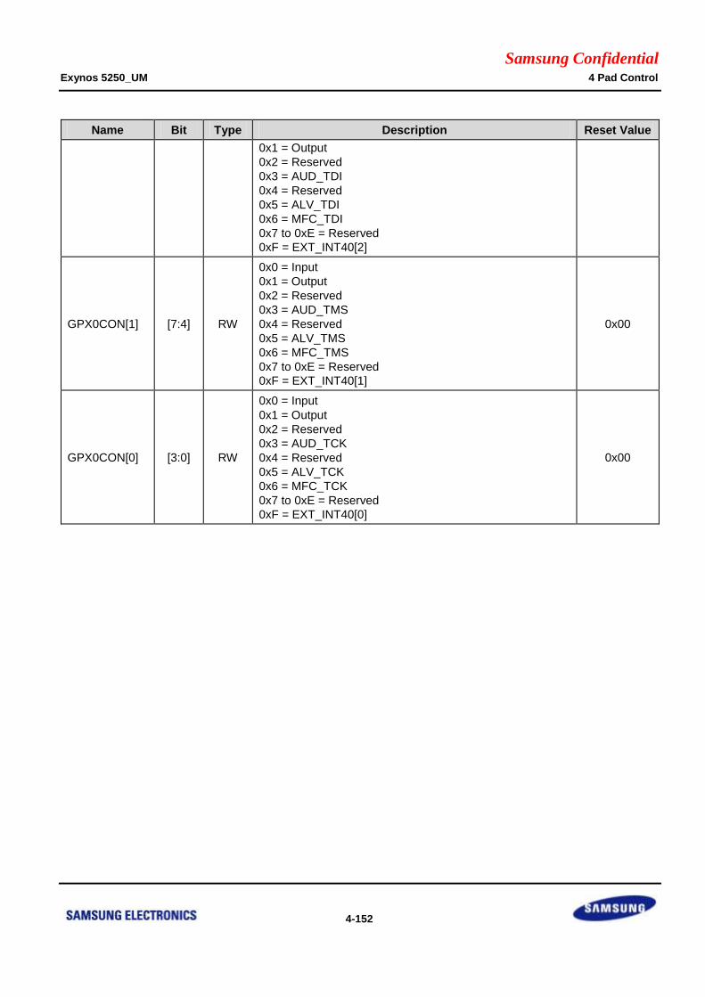
Samsung Confidential Exynos 5250_UM 4 Pad Control
4-152
Name Bit Type Description Reset Value
0x1 = Output
0x2 = Reserved
0x3 = AUD_TDI
0x4 = Reserved
0x5 = ALV_TDI
0x6 = MFC_TDI
0x7 to 0xE = Reserved
0xF = EXT_INT40[2]
GPX0CON[1] [7:4] RW
0x0 = Input
0x1 = Output
0x2 = Reserved
0x3 = AUD_TMS
0x4 = Reserved
0x5 = ALV_TMS
0x6 = MFC_TMS
0x7 to 0xE = Reserved
0xF = EXT_INT40[1]
0x00
GPX0CON[0] [3:0] RW
0x0 = Input
0x1 = Output
0x2 = Reserved
0x3 = AUD_TCK
0x4 = Reserved
0x5 = ALV_TCK
0x6 = MFC_TCK
0x7 to 0xE = Reserved
0xF = EXT_INT40[0]
0x00

Samsung Confidential Exynos 5250_UM 4 Pad Control
4-153
4.4.1.223 GPX0DAT
Base Address: 0x1140_0000
Address = Base Address + 0x0C04, Reset Value = 0x00
Name Bit Type Description Reset Value
GPX0DAT[7:0] [7:0] RWX
When you configure the port as input port, the
corresponding bit is the pin state. When you configure
the port as output port, the pin state is the same as the
corresponding bit. When you configure the port as
functional pin, the undefined value will be read.
0x00
4.4.1.224 GPX0PUD
Base Address: 0x1140_0000
Address = Base Address + 0x0C08, Reset Value = 0x5555
Name Bit Type Description Reset Value
GPX0PUD[n] [2n + 1:2n]
n = 0 to 7 RW
0x0 = Disables Pull-up/down
0x1 = Enables Pull-down
0x2 = Reserved
0x3 = Enables Pull-up
0x5555
4.4.1.225 GPX0DRV
Base Address: 0x1140_0000
Address = Base Address + 0x0C0C, Reset Value = 0x00_0000
Name Bit Type Description Reset Value
GPX0DRV[n]
[2n + 1:2n]
n = 0 to 7 RW
0x0 = 1x
0x2 = 2x
0x1 = 3x
0x3 = 4x
0x00_0000
[n + 16:16]
n = 0 to 7 RW Reserved. Should be zero. 0x00_0000

Samsung Confidential Exynos 5250_UM 4 Pad Control
4-154
4.4.1.226 GPX1CON
Base Address: 0x1140_0000
Address = Base Address + 0x0C20, Reset Value = 0x0000_0000
Name Bit Type Description Reset Value
GPX1CON[7] [31:28] RW
0x0 = Input
0x1 = Output
0x2 = Reserved
0x3 = Reserved
0x4 = Reserved
0x5 = ALV_DBG[11]
0x6 to 0xE = Reserved
0xF = EXT_INT41[7]
0x00
GPX1CON[6] [27:24] RW
0x0 = Input
0x1 = Output
0x2 = Reserved
0x3 = Reserved
0x4 = Reserved
0x5 = ALV_DBG[10]
0x6 to 0xE = Reserved
0xF = EXT_INT41[6]
0x00
GPX1CON[5] [23:20] RW
0x0 = Input
0x1 = Output
0x2 = Reserved
0x3 = Reserved
0x4 = Reserved
0x5 = ALV_DBG[9]
0x6 to 0xE = Reserved
0xF = EXT_INT41[5]
0x00
GPX1CON[4] [19:16] RW
0x0 = Input
0x1 = Output
0x2 = Reserved
0x3 = Reserved
0x4 = Reserved
0x5 = ALV_DBG[8]
0x6 to 0xE = Reserved
0xF = EXT_INT41[4]
0x00
GPX1CON[3] [15:12] RW
0x0 = Input
0x1 = Output
0x2 = Reserved
0x3 = Reserved
0x4 = Reserved
0x5 = ALV_DBG[7]
0x6 to 0xE = Reserved
0xF = EXT_INT41[3]
0x00
GPX1CON[2] [11:8] RW
0x0 = Input
0x1 = Output
0x2 = Reserved
0x3 = Reserved
0x00
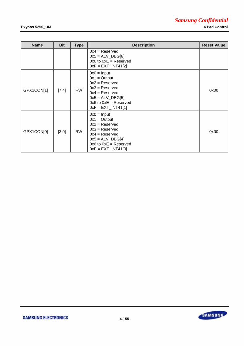
Samsung Confidential Exynos 5250_UM 4 Pad Control
4-155
Name Bit Type Description Reset Value
0x4 = Reserved
0x5 = ALV_DBG[6]
0x6 to 0xE = Reserved
0xF = EXT_INT41[2]
GPX1CON[1] [7:4] RW
0x0 = Input
0x1 = Output
0x2 = Reserved
0x3 = Reserved
0x4 = Reserved
0x5 = ALV_DBG[5]
0x6 to 0xE = Reserved
0xF = EXT_INT41[1]
0x00
GPX1CON[0] [3:0] RW
0x0 = Input
0x1 = Output
0x2 = Reserved
0x3 = Reserved
0x4 = Reserved
0x5 = ALV_DBG[4]
0x6 to 0xE = Reserved
0xF = EXT_INT41[0]
0x00

Samsung Confidential Exynos 5250_UM 4 Pad Control
4-156
4.4.1.227 GPX1DAT
Base Address: 0x1140_0000
Address = Base Address + 0x0C24, Reset Value = 0x00
Name Bit Type Description Reset Value
GPX1DAT[7:0] [7:0] RWX
When you configure the port as input port, the
corresponding bit is the pin state. When you configure
the port as output port, the pin state is the same as the
corresponding bit. When you configure the port as
functional pin, the undefined value will be read.
0x00
4.4.1.228 GPX1PUD
Base Address: 0x1140_0000
Address = Base Address + 0x0C28, Reset Value = 0x5555
Name Bit Type Description Reset Value
GPX1PUD[n] [2n + 1:2n]
n = 0 to 7 RW
0x0 = Disables Pull-up/down
0x1 = Enables Pull-down
0x2 = Reserved
0x3 = Enables Pull-up
0x5555
4.4.1.229 GPX1DRV
Base Address: 0x1140_0000
Address = Base Address + 0x0C2C, Reset Value = 0x00_0000
Name Bit Type Description Reset Value
GPX1DRV[n]
[2n + 1:2n]
n = 0 to 7 RW
0x0 = 1x
0x2 = 2x
0x1 = 3x
0x3 = 4x
0x00_0000
[n + 16:16]
n = 0 to 7 RW Reserved. Should be zero. 0x00_0000

Samsung Confidential Exynos 5250_UM 4 Pad Control
4-157
4.4.1.230 GPX2CON
Base Address: 0x1140_0000
Address = Base Address + 0x0C40, Reset Value = 0x0000_0000
Name Bit Type Description Reset Value
GPX2CON[7] [31:28] RW
0x0 = Input
0x1 = Output
0x2 = Reserved
0x3 = Reserved
0x4 = Reserved
0x5 = ALV_DBG[19]
0x6 to 0xE = Reserved
0xF = EXT_INT42[7]
0x00
GPX2CON[6] [27:24] RW
0x0 = Input
0x1 = Output
0x2 = Reserved
0x3 = Reserved
0x4 = Reserved
0x5 = ALV_DBG[18]
0x6 to 0xE = Reserved
0xF = EXT_INT42[6]
0x00
GPX2CON[5] [23:20] RW
0x0 = Input
0x1 = Output
0x2 = Reserved
0x3 = Reserved
0x4 = Reserved
0x5 = ALV_DBG[17]
0x6 to 0xE = Reserved
0xF = EXT_INT42[5]
0x00
GPX2CON[4] [19:16] RW
0x0 = Input
0x1 = Output
0x2 = Reserved
0x3 = Reserved
0x4 = Reserved
0x5 = ALV_DBG[16]
0x6 to 0xE = Reserved
0xF = EXT_INT42[4]
0x00
GPX2CON[3] [15:12] RW
0x0 = Input
0x1 = Output
0x2 = Reserved
0x3 = Reserved
0x4 = Reserved
0x5 = ALV_DBG[15]
0x6 to 0xE = Reserved
0xF = EXT_INT42[3]
0x00
GPX2CON[2] [11:8] RW
0x0 = Input
0x1 = Output
0x2 = Reserved
0x3 = Reserved
0x00

Samsung Confidential Exynos 5250_UM 4 Pad Control
4-158
Name Bit Type Description Reset Value
0x4 = Reserved
0x5 = ALV_DBG[14]
0x6 to 0xE = Reserved
0xF = EXT_INT42[2]
GPX2CON[1] [7:4] RW
0x0 = Input
0x1 = Output
0x2 = Reserved
0x3 = Reserved
0x4 = Reserved
0x5 = ALV_DBG[13]
0x6 to 0xE = Reserved
0xF = EXT_INT42[1]
0x00
GPX2CON[0] [3:0] RW
0x0 = Input
0x1 = Output
0x2 = Reserved
0x3 = Reserved
0x4 = Reserved
0x5 = ALV_DBG[12]
0x6 to 0xE = Reserved
0xF = EXT_INT42[0]
0x00

Samsung Confidential Exynos 5250_UM 4 Pad Control
4-159
4.4.1.231 GPX2DAT
Base Address: 0x1140_0000
Address = Base Address + 0x0C44, Reset Value = 0x00
Name Bit Type Description Reset Value
GPX2DAT[7:0] [7:0] RWX
When you configure the port as input port, the
corresponding bit is the pin state. When you configure
the port as output port, the pin state is the same as the
corresponding bit. When you configure the port as
functional pin, the undefined value will be read.
0x00
4.4.1.232 GPX2PUD
Base Address: 0x1140_0000
Address = Base Address + 0x0C48, Reset Value = 0x5555
Name Bit Type Description Reset Value
GPX2PUD[n] [2n + 1:2n]
n = 0 to 7 RW
0x0 = Disables Pull-up/down
0x1 = Enables Pull-down
0x2 = Reserved
0x3 = Enables Pull-up
0x5555
4.4.1.233 GPX2DRV
Base Address: 0x1140_0000
Address = Base Address + 0x0C4C, Reset Value = 0x00_0000
Name Bit Type Description Reset Value
GPX2DRV[n]
[2n + 1:2n]
n = 0 to 7 RW
0x0 = 1x
0x2 = 2x
0x1 = 3x
0x3 = 4x
0x00_0000
[n + 16:16]
n = 0 to 7 RW Reserved. Should be zero. 0x00_0000
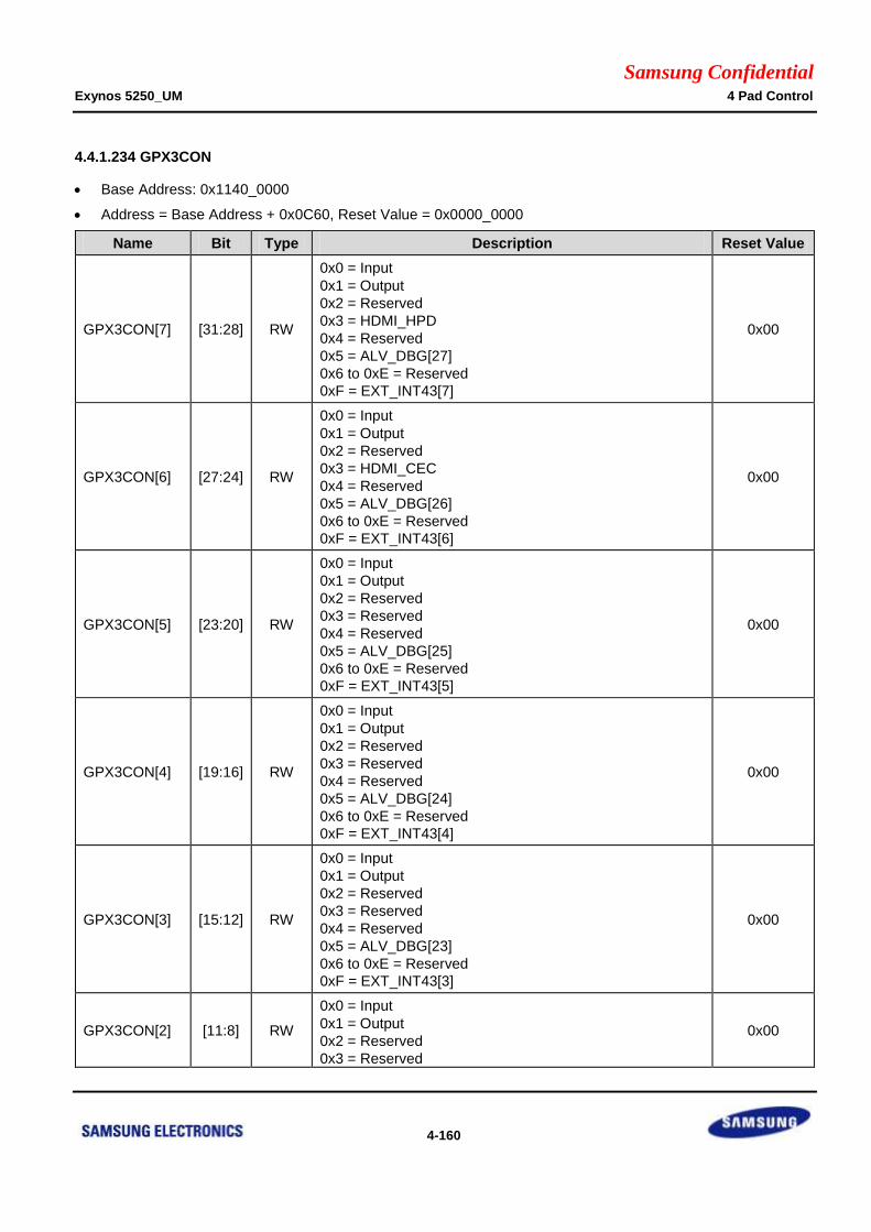
Samsung Confidential Exynos 5250_UM 4 Pad Control
4-160
4.4.1.234 GPX3CON
Base Address: 0x1140_0000
Address = Base Address + 0x0C60, Reset Value = 0x0000_0000
Name Bit Type Description Reset Value
GPX3CON[7] [31:28] RW
0x0 = Input
0x1 = Output
0x2 = Reserved
0x3 = HDMI_HPD
0x4 = Reserved
0x5 = ALV_DBG[27]
0x6 to 0xE = Reserved
0xF = EXT_INT43[7]
0x00
GPX3CON[6] [27:24] RW
0x0 = Input
0x1 = Output
0x2 = Reserved
0x3 = HDMI_CEC
0x4 = Reserved
0x5 = ALV_DBG[26]
0x6 to 0xE = Reserved
0xF = EXT_INT43[6]
0x00
GPX3CON[5] [23:20] RW
0x0 = Input
0x1 = Output
0x2 = Reserved
0x3 = Reserved
0x4 = Reserved
0x5 = ALV_DBG[25]
0x6 to 0xE = Reserved
0xF = EXT_INT43[5]
0x00
GPX3CON[4] [19:16] RW
0x0 = Input
0x1 = Output
0x2 = Reserved
0x3 = Reserved
0x4 = Reserved
0x5 = ALV_DBG[24]
0x6 to 0xE = Reserved
0xF = EXT_INT43[4]
0x00
GPX3CON[3] [15:12] RW
0x0 = Input
0x1 = Output
0x2 = Reserved
0x3 = Reserved
0x4 = Reserved
0x5 = ALV_DBG[23]
0x6 to 0xE = Reserved
0xF = EXT_INT43[3]
0x00
GPX3CON[2] [11:8] RW
0x0 = Input
0x1 = Output
0x2 = Reserved
0x3 = Reserved
0x00

Samsung Confidential Exynos 5250_UM 4 Pad Control
4-161
Name Bit Type Description Reset Value
0x4 = Reserved
0x5 = ALV_DBG[22]
0x6 to 0xE = Reserved
0xF = EXT_INT43[2]
GPX3CON[1] [7:4] RW
0x0 = Input
0x1 = Output
0x2 = Reserved
0x3 = Reserved
0x4 = Reserved
0x5 = ALV_DBG[21]
0x6 to 0xE = Reserved
0xF = EXT_INT43[1]
0x00
GPX3CON[0] [3:0] RW
0x0 = Input
0x1 = Output
0x2 = Reserved
0x3 = Reserved
0x4 = Reserved
0x5 = ALV_DBG[20]
0x6 to 0xE = Reserved
0xF = EXT_INT43[0]
0x00

Samsung Confidential Exynos 5250_UM 4 Pad Control
4-162
4.4.1.235 GPX3DAT
Base Address: 0x1140_0000
Address = Base Address + 0x0C64, Reset Value = 0x00
Name Bit Type Description Reset Value
GPX3DAT[7:0] [7:0] RWX
When you configure the port as input port, the
corresponding bit is the pin state. When you configure
the port as output port, the pin state is the same as the
corresponding bit. When you configure the port as
functional pin, the undefined value will be read.
0x00
4.4.1.236 GPX3PUD
Base Address: 0x1140_0000
Address = Base Address + 0x0C68, Reset Value = 0x5555
Name Bit Type Description Reset Value
GPX3PUD[n] [2n + 1:2n]
n = 0 to 7 RW
0x0 = Disables Pull-up/down
0x1 = Enables Pull-down
0x2 = Reserved
0x3 = Enables Pull-up
0x5555
4.4.1.237 GPX3DRV
Base Address: 0x1140_0000
Address = Base Address + 0x0C6C, Reset Value = 0x00_0000
Name Bit Type Description Reset Value
GPX3DRV[n]
[2n + 1:2n]
n = 0 to 7 RW
0x0 = 1x
0x2 = 2x
0x1 = 3x
0x3 = 4x
0x00_0000
[n + 16:16]
n = 0 to 7 RW Reserved. Should be zero. 0x00_0000
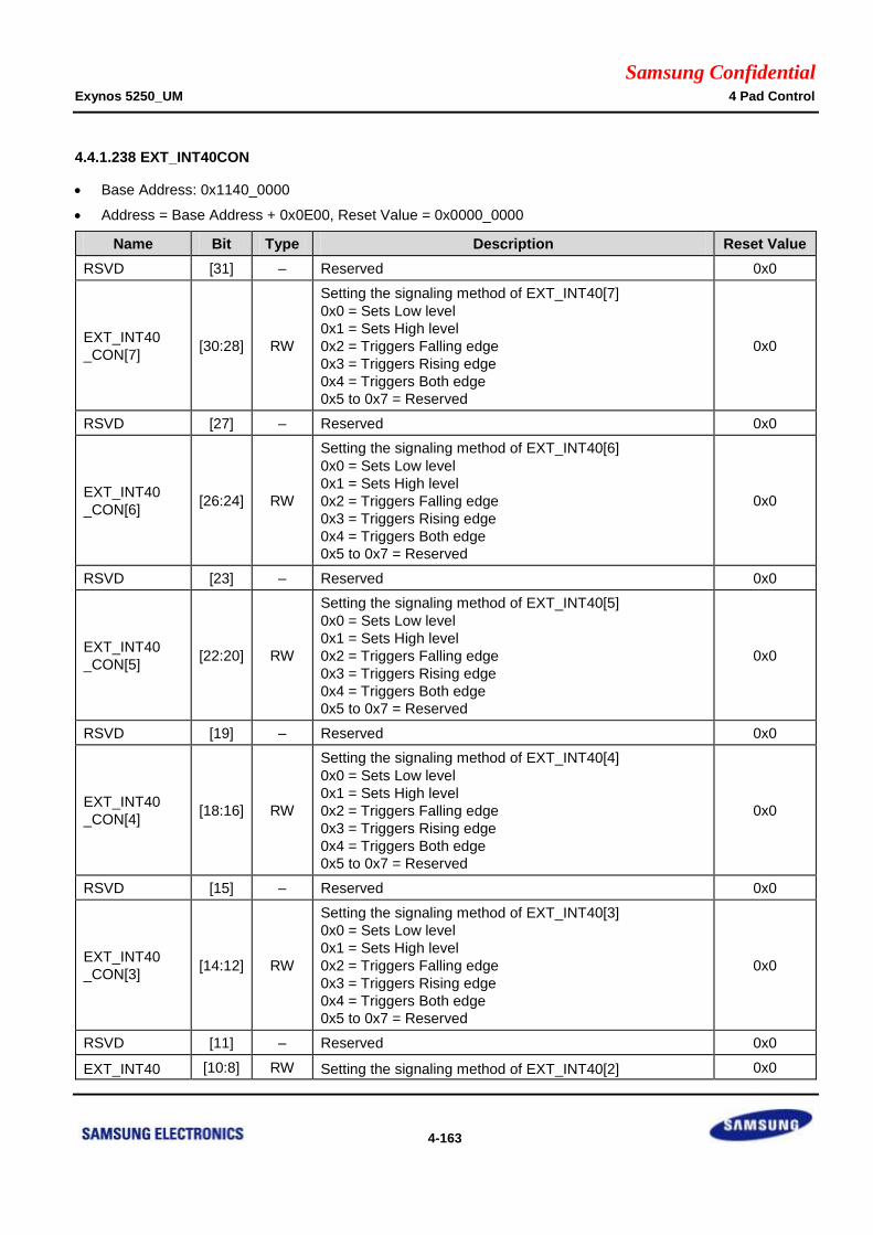
Samsung Confidential Exynos 5250_UM 4 Pad Control
4-163
4.4.1.238 EXT_INT40CON
Base Address: 0x1140_0000
Address = Base Address + 0x0E00, Reset Value = 0x0000_0000
Name Bit Type Description Reset Value
RSVD [31] – Reserved 0x0
EXT_INT40
_CON[7] [30:28] RW
Setting the signaling method of EXT_INT40[7]
0x0 = Sets Low level
0x1 = Sets High level
0x2 = Triggers Falling edge
0x3 = Triggers Rising edge
0x4 = Triggers Both edge
0x5 to 0x7 = Reserved
0x0
RSVD [27] – Reserved 0x0
EXT_INT40
_CON[6] [26:24] RW
Setting the signaling method of EXT_INT40[6]
0x0 = Sets Low level
0x1 = Sets High level
0x2 = Triggers Falling edge
0x3 = Triggers Rising edge
0x4 = Triggers Both edge
0x5 to 0x7 = Reserved
0x0
RSVD [23] – Reserved 0x0
EXT_INT40
_CON[5] [22:20] RW
Setting the signaling method of EXT_INT40[5]
0x0 = Sets Low level
0x1 = Sets High level
0x2 = Triggers Falling edge
0x3 = Triggers Rising edge
0x4 = Triggers Both edge
0x5 to 0x7 = Reserved
0x0
RSVD [19] – Reserved 0x0
EXT_INT40
_CON[4] [18:16] RW
Setting the signaling method of EXT_INT40[4]
0x0 = Sets Low level
0x1 = Sets High level
0x2 = Triggers Falling edge
0x3 = Triggers Rising edge
0x4 = Triggers Both edge
0x5 to 0x7 = Reserved
0x0
RSVD [15] – Reserved 0x0
EXT_INT40
_CON[3] [14:12] RW
Setting the signaling method of EXT_INT40[3]
0x0 = Sets Low level
0x1 = Sets High level
0x2 = Triggers Falling edge
0x3 = Triggers Rising edge
0x4 = Triggers Both edge
0x5 to 0x7 = Reserved
0x0
RSVD [11] – Reserved 0x0
EXT_INT40 [10:8] RW Setting the signaling method of EXT_INT40[2] 0x0

Samsung Confidential Exynos 5250_UM 4 Pad Control
4-164
Name Bit Type Description Reset Value
_CON[2] 0x0 = Sets Low level
0x1 = Sets High level
0x2 = Triggers Falling edge
0x3 = Triggers Rising edge
0x4 = Triggers Both edge
0x5 to 0x7 = Reserved
RSVD [7] – Reserved 0x0
EXT_INT40
_CON[1] [6:4] RW
Setting the signaling method of EXT_INT40[1]
0x0 = Sets Low level
0x1 = Sets High level
0x2 = Triggers Falling edge
0x3 = Triggers Rising edge
0x4 = Triggers Both edge
0x5 to 0x7 = Reserved
0x0
RSVD [3] – Reserved 0x0
EXT_INT40
_CON[0] [2:0] RW
Setting the signaling method of EXT_INT40[0]
0x0 = Sets Low level
0x1 = Sets High level
0x2 = Triggers Falling edge
0x3 = Triggers Rising edge
0x4 = Triggers Both edge
0x5 to 0x7 = Reserved
0x0

Samsung Confidential Exynos 5250_UM 4 Pad Control
4-165
4.4.1.239 EXT_INT42CON
Base Address: 0x1140_0000
Address = Base Address + 0x0E04, Reset Value = 0x0000_0000
Name Bit Type Description Reset Value
RSVD [31] – Reserved 0x0
EXT_INT41
_CON[7] [30:28] RW
Setting the signaling method of EXT_INT41[7]
0x0 = Sets Low level
0x1 = Sets High level
0x2 = Triggers Falling edge
0x3 = Triggers Rising edge
0x4 = Triggers Both edge
0x5 to 0x7 = Reserved
0x0
RSVD [27] – Reserved 0x0
EXT_INT41
_CON[6] [26:24] RW
Setting the signaling method of EXT_INT41[6]
0x0 = Sets Low level
0x1 = Sets High level
0x2 = Triggers Falling edge
0x3 = Triggers Rising edge
0x4 = Triggers Both edge
0x5 to 0x7 = Reserved
0x0
RSVD [23] – Reserved 0x0
EXT_INT41
_CON[5] [22:20] RW
Setting the signaling method of EXT_INT41[5]
0x0 = Sets Low level
0x1 = Sets High level
0x2 = Triggers Falling edge
0x3 = Triggers Rising edge
0x4 = Triggers Both edge
0x5 to 0x7 = Reserved
0x0
RSVD [19] – Reserved 0x0
EXT_INT41
_CON[4] [18:16] RW
Setting the signaling method of EXT_INT41[4]
0x0 = Sets Low level
0x1 = Sets High level
0x2 = Triggers Falling edge
0x3 = Triggers Rising edge
0x4 = Triggers Both edge
0x5 to 0x7 = Reserved
0x0
RSVD [15] – Reserved 0x0
EXT_INT41
_CON[3] [14:12] RW
Setting the signaling method of EXT_INT41[3]
0x0 = Sets Low level
0x1 = Sets High level
0x2 = Triggers Falling edge
0x3 = Triggers Rising edge
0x4 = Triggers Both edge
0x5 to 0x7 = Reserved
0x0
RSVD [11] – Reserved 0x0
EXT_INT41 [10:8] RW Setting the signaling method of EXT_INT41[2] 0x0

Samsung Confidential Exynos 5250_UM 4 Pad Control
4-166
Name Bit Type Description Reset Value
_CON[2] 0x0 = Sets Low level
0x1 = Sets High level
0x2 = Triggers Falling edge
0x3 = Triggers Rising edge
0x4 = Triggers Both edge
0x5 to 0x7 = Reserved
RSVD [7] – Reserved 0x0
EXT_INT41
_CON[1] [6:4] RW
Setting the signaling method of EXT_INT41[1]
0x0 = Sets Low level
0x1 = Sets High level
0x2 = Triggers Falling edge
0x3 = Triggers Rising edge
0x4 = Triggers Both edge
0x5 to 0x7 = Reserved
0x0
RSVD [3] – Reserved 0x0
EXT_INT41
_CON[0] [2:0] RW
Setting the signaling method of EXT_INT41[0]
0x0 = Sets Low level
0x1 = Sets High level
0x2 = Triggers Falling edge
0x3 = Triggers Rising edge
0x4 = Triggers Both edge
0x5 to 0x7 = Reserved
0x0

Samsung Confidential Exynos 5250_UM 4 Pad Control
4-167
4.4.1.240 EXT_INT42CON
Base Address: 0x1140_0000
Address = Base Address + 0x0E08, Reset Value = 0x0000_0000
Name Bit Type Description Reset Value
RSVD [31] – Reserved 0x0
EXT_INT42
_CON[7] [30:28] RW
Setting the signaling method of EXT_INT42[7]
0x0 = Sets Low level
0x1 = Sets High level
0x2 = Triggers Falling edge
0x3 = Triggers Rising edge
0x4 = Triggers Both edge
0x5 to 0x7 = Reserved
0x0
RSVD [27] – Reserved 0x0
EXT_INT42
_CON[6] [26:24] RW
Setting the signaling method of EXT_INT42[6]
0x0 = Sets Low level
0x1 = Sets High level
0x2 = Triggers Falling edge
0x3 = Triggers Rising edge
0x4 = Triggers Both edge
0x5 to 0x7 = Reserved
0x0
RSVD [23] – Reserved 0x0
EXT_INT42
_CON[5] [22:20] RW
Setting the signaling method of EXT_INT42[5]
0x0 = Sets Low level
0x1 = Sets High level
0x2 = Triggers Falling edge
0x3 = Triggers Rising edge
0x4 = Triggers Both edge
0x5 to 0x7 = Reserved
0x0
RSVD [19] – Reserved 0x0
EXT_INT42
_CON[4] [18:16] RW
Setting the signaling method of EXT_INT42[4]
0x0 = Sets Low level
0x1 = Sets High level
0x2 = Triggers Falling edge
0x3 = Triggers Rising edge
0x4 = Triggers Both edge
0x5 to 0x7 = Reserved
0x0
RSVD [15] – Reserved 0x0
EXT_INT42
_CON[3] [14:12] RW
Setting the signaling method of EXT_INT42[3]
0x0 = Sets Low level
0x1 = Sets High level
0x2 = Triggers Falling edge
0x3 = Triggers Rising edge
0x4 = Triggers Both edge
0x5 to 0x7 = Reserved
0x0
RSVD [11] – Reserved 0x0
EXT_INT42 [10:8] RW Setting the signaling method of EXT_INT42[2] 0x0

Samsung Confidential Exynos 5250_UM 4 Pad Control
4-168
Name Bit Type Description Reset Value
_CON[2] 0x0 = Sets Low level
0x1 = Sets High level
0x2 = Triggers Falling edge
0x3 = Triggers Rising edge
0x4 = Triggers Both edge
0x5 to 0x7 = Reserved
RSVD [7] – Reserved 0x0
EXT_INT42
_CON[1] [6:4] RW
Setting the signaling method of EXT_INT42[1]
0x0 = Sets Low level
0x1 = Sets High level
0x2 = Triggers Falling edge
0x3 = Triggers Rising edge
0x4 = Triggers Both edge
0x5 to 0x7 = Reserved
0x0
RSVD [3] – Reserved 0x0
EXT_INT42
_CON[0] [2:0] RW
Setting the signaling method of EXT_INT42[0]
0x0 = Sets Low level
0x1 = Sets High level
0x2 = Triggers Falling edge
0x3 = Triggers Rising edge
0x4 = Triggers Both edge
0x5 to 0x7 = Reserved
0x0

Samsung Confidential Exynos 5250_UM 4 Pad Control
4-169
4.4.1.241 EXT_INT43CON
Base Address: 0x1140_0000
Address = Base Address + 0x0E0C, Reset Value = 0x0000_0000
Name Bit Type Description Reset Value
RSVD [31] – Reserved 0x0
EXT_INT43
_CON[7] [30:28] RW
Setting the signaling method of EXT_INT43[7]
0x0 = Sets Low level
0x1 = Sets High level
0x2 = Triggers Falling edge
0x3 = Triggers Rising edge
0x4 = Triggers Both edge
0x5 to 0x7 = Reserved
0x0
RSVD [27] – Reserved 0x0
EXT_INT43
_CON[6] [26:24] RW
Setting the signaling method of EXT_INT43[6]
0x0 = Sets Low level
0x1 = Sets High level
0x2 = Triggers Falling edge
0x3 = Triggers Rising edge
0x4 = Triggers Both edge
0x5 to 0x7 = Reserved
0x0
RSVD [23] – Reserved 0x0
EXT_INT43
_CON[5] [22:20] RW
Setting the signaling method of EXT_INT43[5]
0x0 = Sets Low level
0x1 = Sets High level
0x2 = Triggers Falling edge
0x3 = Triggers Rising edge
0x4 = Triggers Both edge
0x5 to 0x7 = Reserved
0x0
RSVD [19] – Reserved 0x0
EXT_INT43
_CON[4] [18:16] RW
Setting the signaling method of EXT_INT43[4]
0x0 = Sets Low level
0x1 = Sets High level
0x2 = Triggers Falling edge
0x3 = Triggers Rising edge
0x4 = Triggers Both edge
0x5 to 0x7 = Reserved
0x0
RSVD [15] – Reserved 0x0
EXT_INT43
_CON[3] [14:12] RW
Setting the signaling method of EXT_INT43[3]
0x0 = Sets Low level
0x1 = Sets High level
0x2 = Triggers Falling edge
0x3 = Triggers Rising edge
0x4 = Triggers Both edge
0x5 to 0x7 = Reserved
0x0
RSVD [11] – Reserved 0x0
EXT_INT43 [10:8] RW Setting the signaling method of EXT_INT43[2] 0x0

Samsung Confidential Exynos 5250_UM 4 Pad Control
4-170
Name Bit Type Description Reset Value
_CON[2] 0x0 = Sets Low level
0x1 = Sets High level
0x2 = Triggers Falling edge
0x3 = Triggers Rising edge
0x4 = Triggers Both edge
0x5 to 0x7 = Reserved
RSVD [7] – Reserved 0x0
EXT_INT43
_CON[1] [6:4] RW
Setting the signaling method of EXT_INT43[1]
0x0 = Sets Low level
0x1 = Sets High level
0x2 = Triggers Falling edge
0x3 = Triggers Rising edge
0x4 = Triggers Both edge
0x5 to 0x7 = Reserved
0x0
RSVD [3] – Reserved 0x0
EXT_INT43
_CON[0] [2:0] RW
Setting the signaling method of EXT_INT43[0]
0x0 = Sets Low level
0x1 = Sets High level
0x2 = Triggers Falling edge
0x3 = Triggers Rising edge
0x4 = Triggers Both edge
0x5 to 0x7 = Reserved
0x0

Samsung Confidential Exynos 5250_UM 4 Pad Control
4-171
4.4.1.242 EXT_INT40_FLTCON0
Base Address: 0x1140_0000
Address = Base Address + 0x0E80, Reset Value = 0x8080_8080
Name Bit Type Description Reset Value
FLTEN14[3] [31] RW
Enables Filter for EXT_INT40[3]
0x0 = Disables
0x1 = Enables
0x1
FLTSEL14[3] [30] RW
Selects Filter for EXT_INT40[3]
0x0 = Delays filter
0x1 = Digital filter (clock count)
0x0
FLTWIDTH14[3] [29:24] RW Filtering width of EXT_INT40[3]
This value is valid when FLTSEL14 (of EXT_INT40) is 0x1. 0x00
FLTEN14[2] [23] RW
Enables Filter for EXT_INT40[2]
0x0 = Disables
0x1 = Enables
0x1
FLTSEL14[2] [22] RW
Selects Filter for EXT_INT40[2]
0x0 = Delays filter
0x1 = Digital filter (clock count)
0x0
FLTWIDTH14[2] [21:16] RW Filtering width of EXT_INT40[2]
This value is valid when FLTSEL14 (of EXT_INT40) is 0x1. 0x00
FLTEN14[1] [15] RW
Enables Filter for EXT_INT40[1]
0x0 = Disables
0x1 = Enables
0x1
FLTSEL14[1] [14] RW
Selects Filter for EXT_INT40[1]
0x0 = Delays filter
0x1 = Digital filter (clock count)
0x0
FLTWIDTH14[1] [13:8] RW Filtering width of EXT_INT40[1]
This value is valid when FLTSEL14 (of EXT_INT40) is 0x1. 0x00
FLTEN14[0] [7] RW
Enables Filter for EXT_INT40[0]
0x0 = Disables
0x1 = Enables
0x1
FLTSEL14[0] [6] RW
Selects Filter for EXT_INT40[0]
0x0 = Delays filter
0x1 = Digital filter (clock count)
0x0
FLTWIDTH14[0] [5:0] RW Filtering width of EXT_INT40[0]
This value is valid when FLTSEL14 (of EXT_INT40) is 0x1. 0x00

Samsung Confidential Exynos 5250_UM 4 Pad Control
4-172
4.4.1.243 EXT_INT40_FLTCON1
Base Address: 0x1140_0000
Address = Base Address + 0x0E84, Reset Value = 0x8080_8080
Name Bit Type Description Reset Value
FLTEN14[7] [31] RW
Enables Filter for EXT_INT40[7]
0x0 = Disables
0x1 = Enables
0x1
FLTSEL14[7] [30] RW
Selects Filter for EXT_INT40[7]
0x0 = Delays filter
0x1 = Digital filter (clock count)
0x0
FLTWIDTH14[7] [29:24] RW Filtering width of EXT_INT40[7]
This value is valid when FLTSEL14 (of EXT_INT40) is 0x1. 0x00
FLTEN14[6] [23] RW
Enables Filter for EXT_INT40[6]
0x0 = Disables
0x1 = Enables
0x1
FLTSEL14[6] [22] RW
Selects Filter for EXT_INT40[6]
0x0 = Delays filter
0x1 = Digital filter (clock count)
0x0
FLTWIDTH14[6] [21:16] RW Filtering width of EXT_INT40[6]
This value is valid when FLTSEL14 (of EXT_INT40) is 0x1. 0x00
FLTEN14[5] [15] RW
Enables Filter for EXT_INT40[5]
0x0 = Disables
0x1 = Enables
0x1
FLTSEL14[5] [14] RW
Selects Filter for EXT_INT40[5]
0x0 = Delays filter
0x1 = Digital filter (clock count)
0x0
FLTWIDTH14[5] [13:8] RW Filtering width of EXT_INT40[5]
This value is valid when FLTSEL14 (of EXT_INT40) is 0x1. 0x00
FLTEN14[4] [7] RW
Enables Filter for EXT_INT40[4]
0x0 = Disables
0x1 = Enables
0x1
FLTSEL14[4] [6] RW
Selects Filter for EXT_INT40[4]
0x0 = Delays filter
0x1 = Digital filter (clock count)
0x0
FLTWIDTH14[4] [5:0] RW Filtering width of EXT_INT40[4]
This value is valid when FLTSEL14 (of EXT_INT40) is 0x1. 0x00

Samsung Confidential Exynos 5250_UM 4 Pad Control
4-173
4.4.1.244 EXT_INT41_FLTCON0
Base Address: 0x1140_0000
Address = Base Address + 0x0E88, Reset Value = 0x8080_8080
Name Bit Type Description Reset Value
FLTEN15[3] [31] RW
Enables Filter for EXT_INT41[3]
0x0 = Disables
0x1 = Enables
0x1
FLTSEL15[3] [30] RW
Selects Filter for EXT_INT41[3]
0x0 = Delays filter
0x1 = Digital filter (clock count)
0x0
FLTWIDTH15[3] [29:24] RW Filtering width of EXT_INT41[3]
This value is valid when FLTSEL15 (of EXT_INT41) is 0x1. 0x00
FLTEN15[2] [23] RW
Enables Filter for EXT_INT41[2]
0x0 = Disables
0x1 = Enables
0x1
FLTSEL15[2] [22] RW
Selects Filter for EXT_INT41[2]
0x0 = Delays filter
0x1 = Digital filter (clock count)
0x0
FLTWIDTH15[2] [21:16] RW Filtering width of EXT_INT41[2]
This value is valid when FLTSEL15 (of EXT_INT41) is 0x1. 0x00
FLTEN15[1] [15] RW
Enables Filter for EXT_INT41[1]
0x0 = Disables
0x1 = Enables
0x1
FLTSEL15[1] [14] RW
Selects Filter for EXT_INT41[1]
0x0 = Delays filter
0x1 = Digital filter (clock count)
0x0
FLTWIDTH15[1] [13:8] RW Filtering width of EXT_INT41[1]
This value is valid when FLTSEL15 (of EXT_INT41) is 0x1. 0x00
FLTEN15[0] [7] RW
Enables Filter for EXT_INT41[0]
0x0 = Disables
0x1 = Enables
0x1
FLTSEL15[0] [6] RW
Selects Filter for EXT_INT41[0]
0x0 = Delays filter
0x1 = Digital filter (clock count)
0x0
FLTWIDTH15[0] [5:0] RW Filtering width of EXT_INT41[0]
This value is valid when FLTSEL15 (of EXT_INT41) is 0x1. 0x00

Samsung Confidential Exynos 5250_UM 4 Pad Control
4-174
4.4.1.245 EXT_INT41_FLTCON1
Base Address: 0x1140_0000
Address = Base Address + 0x0E8C, Reset Value = 0x8080_8080
Name Bit Type Description Reset Value
FLTEN15[7] [31] RW
Enables Filter for EXT_INT41[7]
0x0 = Disables
0x1 = Enables
0x1
FLTSEL15[7] [30] RW
Selects Filter for EXT_INT41[7]
0x0 = Delays filter
0x1 = Digital filter (clock count)
0x0
FLTWIDTH15[7] [29:24] RW Filtering width of EXT_INT41[7]
This value is valid when FLTSEL15 (of EXT_INT41) is 0x1. 0x00
FLTEN15[6] [23] RW
Enables Filter for EXT_INT41[6]
0x0 = Disables
0x1 = Enables
0x1
FLTSEL15[6] [22] RW
Selects Filter for EXT_INT41[6]
0x0 = Delays filter
0x1 = Digital filter (clock count)
0x0
FLTWIDTH15[6] [21:16] RW Filtering width of EXT_INT41[6]
This value is valid when FLTSEL15 (of EXT_INT41) is 0x1. 0x00
FLTEN15[5] [15] RW
Enables Filter for EXT_INT41[5]
0x0 = Disables
0x1 = Enables
0x1
FLTSEL15[5] [14] RW
Selects Filter for EXT_INT41[5]
0x0 = Delays filter
0x1 = Digital filter (clock count)
0x0
FLTWIDTH15[5] [13:8] RW Filtering width of EXT_INT41[5]
This value is valid when FLTSEL15 (of EXT_INT41) is 0x1. 0x00
FLTEN15[4] [7] RW
Enables Filter for EXT_INT41[4]
0x0 = Disables
0x1 = Enables
0x1
FLTSEL15[4] [6] RW
Selects Filter for EXT_INT41[4]
0x0 = Delays filter
0x1 = Digital filter (clock count)
0x0
FLTWIDTH15[4] [5:0] RW Filtering width of EXT_INT41[4]
This value is valid when FLTSEL15 (of EXT_INT41) is 0x1. 0x00

Samsung Confidential Exynos 5250_UM 4 Pad Control
4-175
4.4.1.246 EXT_INT42_FLTCON0
Base Address: 0x1140_0000
Address = Base Address + 0x0E90, Reset Value = 0x8080_8080
Name Bit Type Description Reset Value
FLTEN16[3] [31] RW
Enables Filter for EXT_INT42[3]
0x0 = Disables
0x1 = Enables
0x1
FLTSEL16[3] [30] RW
Selects Filter for EXT_INT42[3]
0x0 = Delays filter
0x1 = Digital filter (clock count)
0x0
FLTWIDTH16[3] [29:24] RW Filtering width of EXT_INT42[3]
This value is valid when FLTSEL16 (of EXT_INT42) is 0x1. 0x00
FLTEN16[2] [23] RW
Enables Filter for EXT_INT42[2]
0x0 = Disables
0x1 = Enables
0x1
FLTSEL16[2] [22] RW
Selects Filter for EXT_INT42[2]
0x0 = Delays filter
0x1 = Digital filter (clock count)
0x0
FLTWIDTH16[2] [21:16] RW Filtering width of EXT_INT42[2]
This value is valid when FLTSEL16 (of EXT_INT42) is 0x1. 0x00
FLTEN16[1] [15] RW
Enables Filter for EXT_INT42[1]
0x0 = Disables
0x1 = Enables
0x1
FLTSEL16[1] [14] RW
Selects Filter for EXT_INT42[1]
0x0 = Delays filter
0x1 = Digital filter (clock count)
0x0
FLTWIDTH16[1] [13:8] RW Filtering width of EXT_INT42[1]
This value is valid when FLTSEL16 (of EXT_INT42) is 0x1. 0x00
FLTEN16[0] [7] RW
Enables Filter for EXT_INT42[0]
0x0 = Disables
0x1 = Enables
0x1
FLTSEL16[0] [6] RW
Selects Filter for EXT_INT42[0]
0x0 = Delays filter
0x1 = Digital filter (clock count)
0x0
FLTWIDTH16[0] [5:0] RW Filtering width of EXT_INT42[0]
This value is valid when FLTSEL16 (of EXT_INT42) is 0x1. 0x00

Samsung Confidential Exynos 5250_UM 4 Pad Control
4-176
4.4.1.247 EXT_INT42_FLTCON1
Base Address: 0x1140_0000
Address = Base Address + 0x0E94, Reset Value = 0x8080_8080
Name Bit Type Description Reset Value
FLTEN16[7] [31] RW
Enables Filter for EXT_INT42[7]
0x0 = Disables
0x1 = Enables
0x1
FLTSEL16[7] [30] RW
Selects Filter for EXT_INT42[7]
0x0 = Delays filter
0x1 = Digital filter (clock count)
0x0
FLTWIDTH16[7] [29:24] RW Filtering width of EXT_INT42[7]
This value is valid when FLTSEL16 (of EXT_INT42) is 0x1. 0x00
FLTEN16[6] [23] RW
Enables Filter for EXT_INT42[6]
0x0 = Disables
0x1 = Enables
0x1
FLTSEL16[6] [22] RW
Selects Filter for EXT_INT42[6]
0x0 = Delays filter
0x1 = Digital filter (clock count)
0x0
FLTWIDTH16[6] [21:16] RW Filtering width of EXT_INT42[6]
This value is valid when FLTSEL16 (of EXT_INT42) is 0x1. 0x00
FLTEN16[5] [15] RW
Enables Filter for EXT_INT42[5]
0x0 = Disables
0x1 = Enables
0x1
FLTSEL16[5] [14] RW
Selects Filter for EXT_INT42[5]
0x0 = Delays filter
0x1 = Digital filter (clock count)
0x0
FLTWIDTH16[5] [13:8] RW Filtering width of EXT_INT42[5]
This value is valid when FLTSEL16 (of EXT_INT42) is 0x1. 0x00
FLTEN16[4] [7] RW
Enables Filter for EXT_INT42[4]
0x0 = Disables
0x1 = Enables
0x1
FLTSEL16[4] [6] RW
Selects Filter for EXT_INT42[4]
0x0 = Delays filter
0x1 = Digital filter (clock count)
0x0
FLTWIDTH16[4] [5:0] RW Filtering width of EXT_INT42[4]
This value is valid when FLTSEL16 (of EXT_INT42) is 0x1. 0x00

Samsung Confidential Exynos 5250_UM 4 Pad Control
4-177
4.4.1.248 EXT_INT43_FLTCON0
Base Address: 0x1140_0000
Address = Base Address + 0x0E98, Reset Value = 0x8080_8080
Name Bit Type Description Reset Value
FLTEN17[3] [31] RW
Enables Filter for EXT_INT43[3]
0x0 = Disables
0x1 = Enables
0x1
FLTSEL17[3] [30] RW
Selects Filter for EXT_INT43[3]
0x0 = Delays filter
0x1 = Digital filter (clock count)
0x0
FLTWIDTH17[3] [29:24] RW Filtering width of EXT_INT43[3]
This value is valid when FLTSEL17 (of EXT_INT43) is 0x1. 0x00
FLTEN17[2] [23] RW
Enables Filter for EXT_INT43[2]
0x0 = Disables
0x1 = Enables
0x1
FLTSEL17[2] [22] RW
Selects Filter for EXT_INT43[2]
0x0 = Delays filter
0x1 = Digital filter (clock count)
0x0
FLTWIDTH17[2] [21:16] RW Filtering width of EXT_INT43[2]
This value is valid when FLTSEL17 (of EXT_INT43) is 0x1. 0x00
FLTEN17[1] [15] RW
Enables Filter for EXT_INT43[1]
0x0 = Disables
0x1 = Enables
0x1
FLTSEL17[1] [14] RW
Selects Filter for EXT_INT43[1]
0x0 = Delays filter
0x1 = Digital filter (clock count)
0x0
FLTWIDTH17[1] [13:8] RW Filtering width of EXT_INT43[1]
This value is valid when FLTSEL17 (of EXT_INT43) is 0x1. 0x00
FLTEN17[0] [7] RW
Enables Filter for EXT_INT43[0]
0x0 = Disables
0x1 = Enables
0x1
FLTSEL17[0] [6] RW
Selects Filter for EXT_INT43[0]
0x0 = Delays filter
0x1 = Digital filter (clock count)
0x0
FLTWIDTH17[0] [5:0] RW Filtering width of EXT_INT43[0]
This value is valid when FLTSEL17 (of EXT_INT43) is 0x1. 0x00

Samsung Confidential Exynos 5250_UM 4 Pad Control
4-178
4.4.1.249 EXT_INT43_FLTCON1
Base Address: 0x1140_0000
Address = Base Address + 0x0E9C, Reset Value = 0x8080_8080
Name Bit Type Description Reset Value
FLTEN17[7] [31] RW
Enables Filter for EXT_INT43[7]
0x0 = Disables
0x1 = Enables
0x1
FLTSEL17[7] [30] RW
Selects Filter for EXT_INT43[7]
0x0 = Delays filter
0x1 = Digital filter (clock count)
0x0
FLTWIDTH17[7] [29:24] RW Filtering width of EXT_INT43[7]
This value is valid when FLTSEL17 (of EXT_INT43) is 0x1. 0x00
FLTEN17[6] [23] RW
Enables Filter for EXT_INT43[6]
0x0 = Disables
0x1 = Enables
0x1
FLTSEL17[6] [22] RW
Selects Filter for EXT_INT43[6]
0x0 = Delays filter
0x1 = Digital filter (clock count)
0x0
FLTWIDTH17[6] [21:16] RW Filtering width of EXT_INT43[6]
This value is valid when FLTSEL17 (of EXT_INT43) is 0x1. 0x00
FLTEN17[5] [15] RW
Enables Filter for EXT_INT43[5]
0x0 = Disables
0x1 = Enables
0x1
FLTSEL17[5] [14] RW
Selects Filter for EXT_INT43[5]
0x0 = Delays filter
0x1 = Digital filter (clock count)
0x0
FLTWIDTH17[5] [13:8] RW Filtering width of EXT_INT43[5]
This value is valid when FLTSEL17 (of EXT_INT43) is 0x1. 0x00
FLTEN17[4] [7] RW
Enables Filter for EXT_INT43[4]
0x0 = Disables
0x1 = Enables
0x1
FLTSEL17[4] [6] RW
Selects Filter for EXT_INT43[4]
0x0 = Delays filter
0x1 = Digital filter (clock count)
0x0
FLTWIDTH17[4] [5:0] RW Filtering width of EXT_INT43[4]
This value is valid when FLTSEL17 (of EXT_INT43) is 0x1. 0x00

Samsung Confidential Exynos 5250_UM 4 Pad Control
4-179
4.4.1.250 EXT_INT40_MASK
Base Address: 0x1140_0000
Address = Base Address + 0x0F00, Reset Value = 0x0000_00FF
Name Bit Type Description Reset Value
RSVD [31:8] – Reserved 0x000000
EXT_INT40
_MASK[7] [7] RW
0x0 = Enables Interrupt
0x1 = Masks Interrupt 0x1
EXT_INT40
_MASK[6] [6] RW
0x0 = Enables Interrupt
0x1 = Masks Interrupt 0x1
EXT_INT40
_MASK[5] [5] RW
0x0 = Enables Interrupt
0x1 = Masks Interrupt 0x1
EXT_INT40
_MASK[4] [4] RW
0x0 = Enables Interrupt
0x1 = Masks Interrupt 0x1
EXT_INT40
_MASK[3] [3] RW
0x0 = Enables Interrupt
0x1 = Masks Interrupt 0x1
EXT_INT40
_MASK[2] [2] RW
0x0 = Enables Interrupt
0x1 = Masks Interrupt 0x1
EXT_INT40
_MASK[1] [1] RW
0x0 = Enables Interrupt
0x1 = Masks Interrupt 0x1
EXT_INT40
_MASK[0] [0] RW
0x0 = Enables Interrupt
0x1 = Masks Interrupt 0x1

Samsung Confidential Exynos 5250_UM 4 Pad Control
4-180
4.4.1.251 EXT_INT41_MASK
Base Address: 0x1140_0000
Address = Base Address + 0x0F04, Reset Value = 0x0000_00FF
Name Bit Type Description Reset Value
RSVD [31:8] – Reserved 0x000000
EXT_INT41
_MASK[7] [7] RW
0x0 = Enables Interrupt
0x1 = Masks Interrupt 0x1
EXT_INT41
_MASK[6] [6] RW
0x0 = Enables Interrupt
0x1 = Masks Interrupt 0x1
EXT_INT41
_MASK[5] [5] RW
0x0 = Enables Interrupt
0x1 = Masks Interrupt 0x1
EXT_INT41
_MASK[4] [4] RW
0x0 = Enables Interrupt
0x1 = Masks Interrupt 0x1
EXT_INT41
_MASK[3] [3] RW
0x0 = Enables Interrupt
0x1 = Masks Interrupt 0x1
EXT_INT41
_MASK[2] [2] RW
0x0 = Enables Interrupt
0x1 = Masks Interrupt 0x1
EXT_INT41
_MASK[1] [1] RW
0x0 = Enables Interrupt
0x1 = Masks Interrupt 0x1
EXT_INT41
_MASK[0] [0] RW
0x0 = Enables Interrupt
0x1 = Masks Interrupt 0x1

Samsung Confidential Exynos 5250_UM 4 Pad Control
4-181
4.4.1.252 EXT_INT42_MASK
Base Address: 0x1140_0000
Address = Base Address + 0x0F08, Reset Value = 0x0000_00FF
Name Bit Type Description Reset Value
RSVD [31:8] – Reserved 0x000000
EXT_INT42
_MASK[7] [7] RW
0x0 = Enables Interrupt
0x1 = Masks Interrupt 0x1
EXT_INT42
_MASK[6] [6] RW
0x0 = Enables Interrupt
0x1 = Masks Interrupt 0x1
EXT_INT42
_MASK[5] [5] RW
0x0 = Enables Interrupt
0x1 = Masks Interrupt 0x1
EXT_INT42
_MASK[4] [4] RW
0x0 = Enables Interrupt
0x1 = Masks Interrupt 0x1
EXT_INT42
_MASK[3] [3] RW
0x0 = Enables Interrupt
0x1 = Masks Interrupt 0x1
EXT_INT42
_MASK[2] [2] RW
0x0 = Enables Interrupt
0x1 = Masks Interrupt 0x1
EXT_INT42
_MASK[1] [1] RW
0x0 = Enables Interrupt
0x1 = Masks Interrupt 0x1
EXT_INT42
_MASK[0] [0] RW
0x0 = Enables Interrupt
0x1 = Masks Interrupt 0x1

Samsung Confidential Exynos 5250_UM 4 Pad Control
4-182
4.4.1.253 EXT_INT43_MASK
Base Address: 0x1140_0000
Address = Base Address + 0x0F0C, Reset Value = 0x0000_00FF
Name Bit Type Description Reset Value
RSVD [31:8] – Reserved 0x000000
EXT_INT43
_MASK[7] [7] RW
0x0 = Enables Interrupt
0x1 = Masks Interrupt 0x1
EXT_INT43
_MASK[6] [6] RW
0x0 = Enables Interrupt
0x1 = Masks Interrupt 0x1
EXT_INT43
_MASK[5] [5] RW
0x0 = Enables Interrupt
0x1 = Masks Interrupt 0x1
EXT_INT43
_MASK[4] [4] RW
0x0 = Enables Interrupt
0x1 = Masks Interrupt 0x1
EXT_INT43
_MASK[3] [3] RW
0x0 = Enables Interrupt
0x1 = Masks Interrupt 0x1
EXT_INT43
_MASK[2] [2] RW
0x0 = Enables Interrupt
0x1 = Masks Interrupt 0x1
EXT_INT43
_MASK[1] [1] RW
0x0 = Enables Interrupt
0x1 = Masks Interrupt 0x1
EXT_INT43
_MASK[0] [0] RW
0x0 = Enables Interrupt
0x1 = Masks Interrupt 0x1

Samsung Confidential Exynos 5250_UM 4 Pad Control
4-183
4.4.1.254 EXT_INT40_PEND
Base Address: 0x1140_0000
Address = Base Address + 0x0F40, Reset Value = 0x0000_0000
Name Bit Type Description Reset Value
RSVD [31:8] – Reserved 0x000000
EXT_INT40
_PEND[7] [7] RWX
0x0 = Does not occur
0x1 = Interrupt occurs 0x0
EXT_INT40
_PEND[6] [6] RWX
0x0 = Does not occur
0x1 = Interrupt occurs 0x0
EXT_INT40
_PEND[5] [5] RWX
0x0 = Does not occur
0x1 = Interrupt occurs 0x0
EXT_INT40
_PEND[4] [4] RWX
0x0 = Does not occur
0x1 = Interrupt occurs 0x0
EXT_INT40
_PEND[3] [3] RWX
0x0 = Does not occur
0x1 = Interrupt occurs 0x0
EXT_INT40
_PEND[2] [2] RWX
0x0 = Does not occur
0x1 = Interrupt occurs 0x0
EXT_INT40
_PEND[1] [1] RWX
0x0 = Does not occur
0x1 = Interrupt occurs 0x0
EXT_INT40
_PEND[0] [0] RWX
0x0 = Does not occur
0x1 = Interrupt occurs 0x0
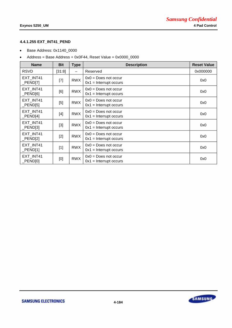
Samsung Confidential Exynos 5250_UM 4 Pad Control
4-184
4.4.1.255 EXT_INT41_PEND
Base Address: 0x1140_0000
Address = Base Address + 0x0F44, Reset Value = 0x0000_0000
Name Bit Type Description Reset Value
RSVD [31:8] – Reserved 0x000000
EXT_INT41
_PEND[7] [7] RWX
0x0 = Does not occur
0x1 = Interrupt occurs 0x0
EXT_INT41
_PEND[6] [6] RWX
0x0 = Does not occur
0x1 = Interrupt occurs 0x0
EXT_INT41
_PEND[5] [5] RWX
0x0 = Does not occur
0x1 = Interrupt occurs 0x0
EXT_INT41
_PEND[4] [4] RWX
0x0 = Does not occur
0x1 = Interrupt occurs 0x0
EXT_INT41
_PEND[3] [3] RWX
0x0 = Does not occur
0x1 = Interrupt occurs 0x0
EXT_INT41
_PEND[2] [2] RWX
0x0 = Does not occur
0x1 = Interrupt occurs 0x0
EXT_INT41
_PEND[1] [1] RWX
0x0 = Does not occur
0x1 = Interrupt occurs 0x0
EXT_INT41
_PEND[0] [0] RWX
0x0 = Does not occur
0x1 = Interrupt occurs 0x0

Samsung Confidential Exynos 5250_UM 4 Pad Control
4-185
4.4.1.256 EXT_INT42_PEND
Base Address: 0x1140_0000
Address = Base Address + 0x0F48, Reset Value = 0x0000_0000
Name Bit Type Description Reset Value
RSVD [31:8] – Reserved 0x000000
EXT_INT42
_PEND[7] [7] RWX
0x0 = Does not occur
0x1 = Interrupt occurs 0x0
EXT_INT42
_PEND[6] [6] RWX
0x0 = Does not occur
0x1 = Interrupt occurs 0x0
EXT_INT42
_PEND[5] [5] RWX
0x0 = Does not occur
0x1 = Interrupt occurs 0x0
EXT_INT42
_PEND[4] [4] RWX
0x0 = Does not occur
0x1 = Interrupt occurs 0x0
EXT_INT42
_PEND[3] [3] RWX
0x0 = Does not occur
0x1 = Interrupt occurs 0x0
EXT_INT42
_PEND[2] [2] RWX
0x0 = Does not occur
0x1 = Interrupt occurs 0x0
EXT_INT42
_PEND[1] [1] RWX
0x0 = Does not occur
0x1 = Interrupt occurs 0x0
EXT_INT42
_PEND[0] [0] RWX
0x0 = Does not occur
0x1 = Interrupt occurs 0x0

Samsung Confidential Exynos 5250_UM 4 Pad Control
4-186
4.4.1.257 EXT_INT43_PEND
Base Address: 0x1140_0000
Address = Base Address + 0x0F4C, Reset Value = 0x0000_0000
Name Bit Type Description Reset Value
RSVD [31:8] – Reserved 0x000000
EXT_INT43
_PEND[7] [7] RWX
0x0 = Does not occur
0x1 = Interrupt occurs 0x0
EXT_INT43
_PEND[6] [6] RWX
0x0 = Does not occur
0x1 = Interrupt occurs 0x0
EXT_INT43
_PEND[5] [5] RWX
0x0 = Does not occur
0x1 = Interrupt occurs 0x0
EXT_INT43
_PEND[4] [4] RWX
0x0 = Does not occur
0x1 = Interrupt occurs 0x0
EXT_INT43
_PEND[3] [3] RWX
0x0 = Does not occur
0x1 = Interrupt occurs 0x0
EXT_INT43
_PEND[2] [2] RWX
0x0 = Does not occur
0x1 = Interrupt occurs 0x0
EXT_INT43
_PEND[1] [1] RWX
0x0 = Does not occur
0x1 = Interrupt occurs 0x0
EXT_INT43
_PEND[0] [0] RWX
0x0 = Does not occur
0x1 = Interrupt occurs 0x0

Samsung Confidential Exynos 5250_UM 4 Pad Control
4-187
4.4.1.258 GPE0CON
Base Address: 0x1340_0000
Address = Base Address + 0x0000, Reset Value = 0x0000_0000
Name Bit Type Description Reset Value
GPE0CON[7] [31:28] RW
0x0 = Input
0x1 = Output
0x2 = CAM_GPIO[7]
0x3 = TXD_UART_ISP
0x4 to 0xE = Reserved
0xF = EXT_INT14[7]
0x00
GPE0CON[6] [27:24] RW
0x0 = Input
0x1 = Output
0x2 = CAM_GPIO[6]
0x3 = nRTS_UART_ISP
0x4 = CAM_I2C2_SDA
0x5 to 0xE = Reserved
0xF = EXT_INT14[6]
0x00
GPE0CON[5] [23:20] RW
0x0 = Input
0x1 = Output
0x2 = CAM_GPIO[5]
0x3 = MPWM6_OUT_ISP
0x4 = CAM_SPI1_MOSI
0x5 to 0xE = Reserved
0xF = EXT_INT14[5]
0x00
GPE0CON[4] [19:16] RW
0x0 = Input
0x1 = Output
0x2 = CAM_GPIO[4]
0x3 = MPWM5_OUT_ISP
0x4 = CAM_SPI1_MISO
0x5 to 0xE = Reserved
0xF = EXT_INT14[4]
0x00
GPE0CON[3] [15:12] RW
0x0 = Input
0x1 = Output
0x2 = CAM_GPIO[3]
0x3 = MPWM4_OUT_ISP
0x4 to 0xE = Reserved
0xF = EXT_INT14[3]
0x00
GPE0CON[2] [11:8] RW
0x0 = Input
0x1 = Output
0x2 = CAM_GPIO[2]
0x3 = MPWM3_OUT_ISP
0x4 to 0xE = Reserved
0xF = EXT_INT14[2]
0x00
GPE0CON[1] [7:4] RW
0x0 = Input
0x1 = Output
0x2 = CAM_GPIO[1]
0x3 = MPWM2_OUT_ISP
0x4 to 0xE = Reserved
0x00
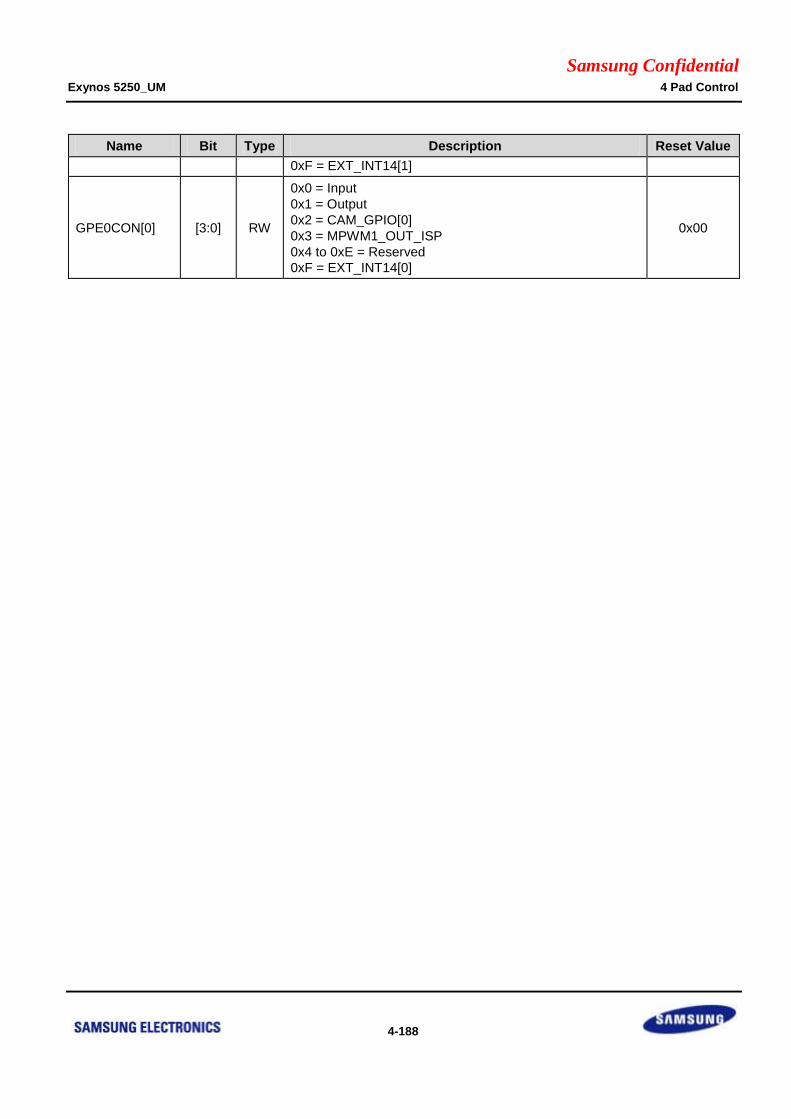
Samsung Confidential Exynos 5250_UM 4 Pad Control
4-188
Name Bit Type Description Reset Value
0xF = EXT_INT14[1]
GPE0CON[0] [3:0] RW
0x0 = Input
0x1 = Output
0x2 = CAM_GPIO[0]
0x3 = MPWM1_OUT_ISP
0x4 to 0xE = Reserved
0xF = EXT_INT14[0]
0x00

Samsung Confidential Exynos 5250_UM 4 Pad Control
4-189
4.4.1.259 GPE0DAT
Base Address: 0x1340_0000
Address = Base Address + 0x0004, Reset Value = 0x00
Name Bit Type Description Reset Value
GPE0DAT[7:0] [7:0] RWX
When you configure the port as input port, the
corresponding bit is the pin state. When you configure
the port as output port, the pin state is the same as the
corresponding bit. When you configure the port as
functional pin, the undefined value will be read.
0x00
4.4.1.260 GPE0PUD
Base Address: 0x1340_0000
Address = Base Address + 0x0008, Reset Value = 0x5555
Name Bit Type Description Reset Value
GPE0PUD[n] [2n + 1:2n]
n = 0 to 7 RW
0x0 = Disables Pull-up/down
0x1 = Enables Pull-down
0x2 = Reserved
0x3 = Enables Pull-up
0x5555
4.4.1.261 GPE0DRV
Base Address: 0x1340_0000
Address = Base Address + 0x000C, Reset Value = 0x00_0000
Name Bit Type Description Reset Value
GPE0DRV[n]
[2n + 1:2n]
n = 0 to 7 RW
0x0 = 1x
0x2 = 2x
0x1 = 3x
0x3 = 4x
0x00_0000
[n + 16:16]
n = 0 to 7 RW Reserved. Should be zero. 0x00_0000
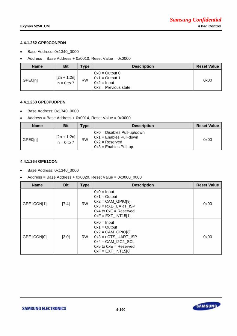
Samsung Confidential Exynos 5250_UM 4 Pad Control
4-190
4.4.1.262 GPE0CONPDN
Base Address: 0x1340_0000
Address = Base Address + 0x0010, Reset Value = 0x0000
Name Bit Type Description Reset Value
GPE0[n] [2n + 1:2n]
n = 0 to 7 RW
0x0 = Output 0
0x1 = Output 1
0x2 = Input
0x3 = Previous state
0x00
4.4.1.263 GPE0PUDPDN
Base Address: 0x1340_0000
Address = Base Address + 0x0014, Reset Value = 0x0000
Name Bit Type Description Reset Value
GPE0[n] [2n + 1:2n]
n = 0 to 7 RW
0x0 = Disables Pull-up/down
0x1 = Enables Pull-down
0x2 = Reserved
0x3 = Enables Pull-up
0x00
4.4.1.264 GPE1CON
Base Address: 0x1340_0000
Address = Base Address + 0x0020, Reset Value = 0x0000_0000
Name Bit Type Description Reset Value
GPE1CON[1] [7:4] RW
0x0 = Input
0x1 = Output
0x2 = CAM_GPIO[9]
0x3 = RXD_UART_ISP
0x4 to 0xE = Reserved
0xF = EXT_INT15[1]
0x00
GPE1CON[0] [3:0] RW
0x0 = Input
0x1 = Output
0x2 = CAM_GPIO[8]
0x3 = nCTS_UART_ISP
0x4 = CAM_I2C2_SCL
0x5 to 0xE = Reserved
0xF = EXT_INT15[0]
0x00

Samsung Confidential Exynos 5250_UM 4 Pad Control
4-191
4.4.1.265 GPE1DAT
Base Address: 0x1340_0000
Address = Base Address + 0x0024, Reset Value = 0x00
Name Bit Type Description Reset Value
GPE1DAT[1:0] [1:0] RWX
When you configure the port as input port, the
corresponding bit is the pin state. When you configure
the port as output port, the pin state is the same as the
corresponding bit. When you configure the port as
functional pin, the undefined value will be read.
0x00
4.4.1.266 GPE1PUD
Base Address: 0x1340_0000
Address = Base Address + 0x0028 Reset Value = 0x0005
Name Bit Type Description Reset Value
GPE1PUD[n] [2n + 1:2n]
n = 0 to 1 RW
0x0 = Disables Pull-up/down
0x1 = Enables Pull-down
0x2 = Reserved
0x3 = Enables Pull-up
0x0005
4.4.1.267 GPE1DRV
Base Address: 0x1340_0000
Address = Base Address + 0x002C, Reset Value = 0x00_0000
Name Bit Type Description Reset Value
GPE1DRV[n]
[2n + 1:2n]
n = 0 to 1 RW
0x0 = 1x
0x2 = 2x
0x1 = 3x
0x3 = 4x
0x00_0000
[n + 16:16]
N = 0 to 1 RW Reserved. Should be zero. 0x00_0000

Samsung Confidential Exynos 5250_UM 4 Pad Control
4-192
4.4.1.268 GPE1CONPDN
Base Address: 0x1340_0000
Address = Base Address + 0x0030, Reset Value = 0x0000
Name Bit Type Description Reset Value
GPE1[n] [2n + 1:2n]
n = 0 to 1 RW
0x0 = Output 0
0x1 = Output 1
0x2 = Input
0x3 = Previous state
0x00
4.4.1.269 GPE1PUDPDN
Base Address: 0x1340_0000
Address = Base Address + 0x0034, Reset Value = 0x0000
Name Bit Type Description Reset Value
GPE1[n] [2n + 1:2n]
n = 0 to 1 RW
0x0 = Disables Pull-up/down
0x1 = Enables Pull-down
0x2 = Reserved
0x3 = Enables Pull-up
0x00

Samsung Confidential Exynos 5250_UM 4 Pad Control
4-193
4.4.1.270 GPF0CON
Base Address: 0x1340_0000
Address = Base Address + 0x0040, Reset Value = 0x0000_0000
Name Bit Type Description Reset Value
GPF0CON[3] [15:12] RW
0x0 = Input
0x1 = Output
0x2 = CAM_I2C1_SCL
0x3 = CAM_GPIO[13]
0x4 = CAM_SPI1_nSS
0x5 to 0xE = Reserved
0xF = EXT_INT16[3]
0x00
GPF0CON[2] [11:8] RW
0x0 = Input
0x1 = Output
0x2 = CAM_I2C1_SDA
0x3 = CAM_GPIO[12]
0x4 = CAM_SPI1_CLK
0x5 to 0xE = Reserved
0xF = EXT_INT16[2]
0x00
GPF0CON[1] [7:4] RW
0x0 = Input
0x1 = Output
0x2 = CAM_I2C0_SCL
0x3 = CAM_GPIO[11]
0x4 to 0xE = Reserved
0xF = EXT_INT16[1]
0x00
GPF0CON[0] [3:0] RW
0x0 = Input
0x1 = Output
0x2 = CAM_I2C0_SDA
0x3 = CAM_GPIO[10]
0x4 to 0xE = Reserved
0xF = EXT_INT16[0]
0x00
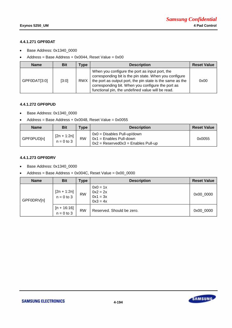
Samsung Confidential Exynos 5250_UM 4 Pad Control
4-194
4.4.1.271 GPF0DAT
Base Address: 0x1340_0000
Address = Base Address + 0x0044, Reset Value = 0x00
Name Bit Type Description Reset Value
GPF0DAT[3:0] [3:0] RWX
When you configure the port as input port, the
corresponding bit is the pin state. When you configure
the port as output port, the pin state is the same as the
corresponding bit. When you configure the port as
functional pin, the undefined value will be read.
0x00
4.4.1.272 GPF0PUD
Base Address: 0x1340_0000
Address = Base Address + 0x0048, Reset Value = 0x0055
Name Bit Type Description Reset Value
GPF0PUD[n] [2n + 1:2n]
n = 0 to 3 RW
0x0 = Disables Pull-up/down
0x1 = Enables Pull-down
0x2 = Reserved0x3 = Enables Pull-up
0x0055
4.4.1.273 GPF0DRV
Base Address: 0x1340_0000
Address = Base Address + 0x004C, Reset Value = 0x00_0000
Name Bit Type Description Reset Value
GPF0DRV[n]
[2n + 1:2n]
n = 0 to 3 RW
0x0 = 1x
0x2 = 2x
0x1 = 3x
0x3 = 4x
0x00_0000
[n + 16:16]
n = 0 to 3 RW Reserved. Should be zero. 0x00_0000
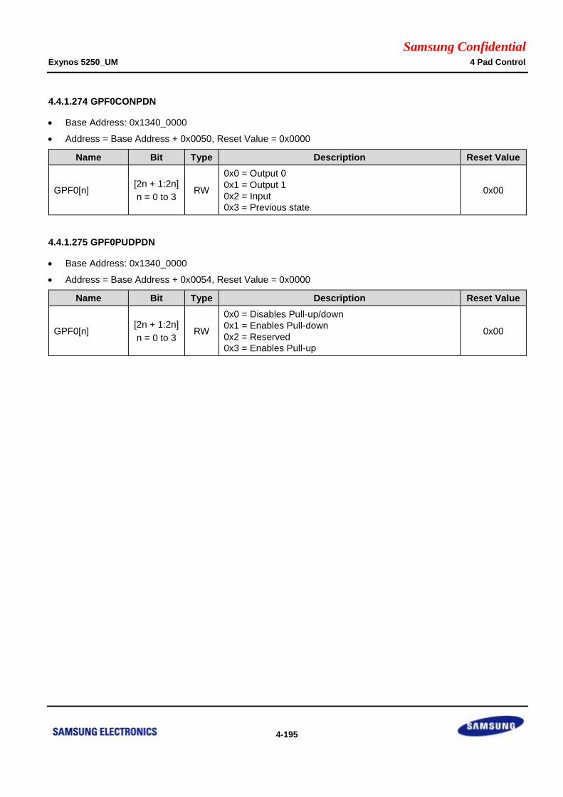
Samsung Confidential Exynos 5250_UM 4 Pad Control
4-195
4.4.1.274 GPF0CONPDN
Base Address: 0x1340_0000
Address = Base Address + 0x0050, Reset Value = 0x0000
Name Bit Type Description Reset Value
GPF0[n] [2n + 1:2n]
n = 0 to 3 RW
0x0 = Output 0
0x1 = Output 1
0x2 = Input
0x3 = Previous state
0x00
4.4.1.275 GPF0PUDPDN
Base Address: 0x1340_0000
Address = Base Address + 0x0054, Reset Value = 0x0000
Name Bit Type Description Reset Value
GPF0[n] [2n + 1:2n]
n = 0 to 3 RW
0x0 = Disables Pull-up/down
0x1 = Enables Pull-down
0x2 = Reserved
0x3 = Enables Pull-up
0x00

Samsung Confidential Exynos 5250_UM 4 Pad Control
4-196
4.4.1.276 GPF1CON
Base Address: 0x1340_0000
Address = Base Address + 0x0060, Reset Value = 0x0000_0000
Name Bit Type Description Reset Value
GPF1CON[3] [15:12] RW
0x0 = Input
0x1 = Output
0x2 = CAM_SPI_MOSI
0x3 = CAM_GPIO[17]
0x4 to 0xE = Reserved
0xF = EXT_INT17[3]
0x00
GPF1CON[2] [11:8] RW
0x0 = Inputs
0x1 = Outputs
0x2 = CAM_SPI_MISO
0x3 = CAM_GPIO[16]
0x4 to 0xE = Reserved
0xF = EXT_INT17[2]
0x00
GPF1CON[1] [7:4] RW
0x0 = Input
0x1 = Output
0x2 = CAM_SPI_nSS
0x3 = CAM_GPIO[15]
0x4 to 0xE = Reserved
0xF = EXT_INT17[1]
0x00
GPF1CON[0] [3:0] RW
0x0 = Input
0x1 = Output
0x2 = CAM_SPI_CLK
0x3 = CAM_GPIO[14]
0x4 to 0xE = Reserved
0xF = EXT_INT17[0]
0x00

Samsung Confidential Exynos 5250_UM 4 Pad Control
4-197
4.4.1.277 GPF1DAT
Base Address: 0x1340_0000
Address = Base Address + 0x0064, Reset Value = 0x00
Name Bit Type Description Reset Value
GPF1DAT[3:0] [3:0] RWX
When you configure the port as input port, the
corresponding bit is the pin state. When you configure
the port as output port, the pin state is the same as the
corresponding bit. When you configure the port as
functional pin, the undefined value will be read.
0x00
4.4.1.278 GPF1PUD
Base Address: 0x1340_0000
Address = Base Address + 0x0068, Reset Value = 0x0055
Name Bit Type Description Reset Value
GPF1PUD[n] [2n + 1:2n]
n = 0 to 3 RW
0x0 = Disables Pull-up/down
0x1 = Enables Pull-down
0x2 = Reserved
0x3 = Enables Pull-up
0x0055
4.4.1.279 GPF1DRV
Base Address: 0x1340_0000
Address = Base Address + 0x006C, Reset Value = 0x00_0000
Name Bit Type Description Reset Value
GPF1DRV[n]
[2n + 1:2n]
n = 0 to 3 RW
0x0 = 1x
0x2 = 2x
0x1 = 3x
0x3 = 4x
0x00_0000
[n + 16:16]
n = 0 to 3 RW Reserved. Should be zero. 0x00_0000

Samsung Confidential Exynos 5250_UM 4 Pad Control
4-198
4.4.1.280 GPF1CONPDN
Base Address: 0x1340_0000
Address = Base Address + 0x0070, Reset Value = 0x0000
Name Bit Type Description Reset Value
GPF1[n] [2n + 1:2n]
n = 0 to 3 RW
0x0 = Output 0
0x1 = Output 1
0x2 = Input
0x3 = Previous state
0x00
4.4.1.281 GPF1PUDPDN
Base Address: 0x1340_0000
Address = Base Address + 0x0074, Reset Value = 0x0000
Name Bit Type Description Reset Value
GPF1[n] [2n + 1:2n]
n = 0 to 3 RW
0x0 = Disables Pull-up/down
0x1 = Enables Pull-down
0x2 = Reserved
0x3 = Enables Pull-up
0x00

Samsung Confidential Exynos 5250_UM 4 Pad Control
4-199
4.4.1.282 GPG0CON
Base Address: 0x1340_0000
Address = Base Address + 0x0080, Reset Value = 0x0000_0000
Name Bit Type Description Reset Value
GPG0CON[7] [31:28] RW
0x0 = Input
0x1 = Output
0x2 = CAM_BAY_RGB[6]
0x3 = TraceData[7]
0x4 to 0xE = Reserved
0xF = EXT_INT18[7]
0x00
GPG0CON[6] [27:24] RW
0x0 = Input
0x1 = Output
0x2 = CAM_BAY_RGB[5]
0x3 = TraceData[6]
0x4 to 0xE = Reserved
0xF = EXT_INT18[6]
0x00
GPG0CON[5] [23:20] RW
0x0 = Input
0x1 = Output
0x2 = CAM_BAY_RGB[4]
0x3 = TraceData[5]
0x4 to 0xE = Reserved
0xF = EXT_INT18[5]
0x00
GPG0CON[4] [19:16] RW
0x0 = Inputs
0x1 = Outputs
0x2 = CAM_BAY_RGB[3]
0x3 = TraceData[4]
0x4 to 0xE = Reserved
0xF = EXT_INT18[4]
0x00
GPG0CON[3] [15:12] RW
0x0 = Input
0x1 = Output
0x2 = CAM_BAY_RGB[2]
0x3 = TraceData[3]
0x4 to 0xE = Reserved
0xF = EXT_INT18[3]
0x00
GPG0CON[2] [11:8] RW
0x0 = Input
0x1 = Output
0x2 = CAM_BAY_RGB[1]
0x3 = TraceData[2]
0x4 to 0xE = Reserved
0xF = EXT_INT18[2]
0x00
GPG0CON[1] [7:4] RW
0x0 = Input
0x1 = Output
0x2 = CAM_BAY_RGB[0]
0x3 = TraceData[1]
0x4 to 0xE = Reserved
0xF = EXT_INT18[1]
0x00
GPG0CON[0] [3:0] RW 0x0 = Input
0x1 = Output 0x00
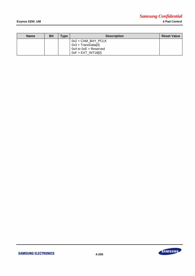
Samsung Confidential Exynos 5250_UM 4 Pad Control
4-200
Name Bit Type Description Reset Value
0x2 = CAM_BAY_PCLK
0x3 = TraceData[0]
0x4 to 0xE = Reserved
0xF = EXT_INT18[0]

Samsung Confidential Exynos 5250_UM 4 Pad Control
4-201
4.4.1.283 GPG0DAT
Base Address: 0x1340_0000
Address = Base Address + 0x0084, Reset Value = 0x00
Name Bit Type Description Reset Value
GPG0DAT[7:0] [7:0] RWX
When you configure the port as input port, the
corresponding bit is the pin state. When you configure
the port as output port, the pin state is the same as the
corresponding bit. When you configure the port as
functional pin, the undefined value will be read.
0x00
4.4.1.284 GPG0PUD
Base Address: 0x1340_0000
Address = Base Address + 0x0088, Reset Value = 0x5555
Name Bit Type Description Reset Value
GPG0PUD[n] [2n + 1:2n]
n = 0 to 7 RW
0x0 = Disables Pull-up/down
0x1 = Enables Pull-down
0x2 = Reserved
0x3 = Enables Pull-up
0x5555
4.4.1.285 GPG0DRV
Base Address: 0x1340_0000
Address = Base Address + 0x008C, Reset Value = 0x00_0000
Name Bit Type Description Reset Value
GPG0DRV[n]
[2n + 1:2n]
n = 0 to 7 RW
0x0 = 1x
0x2 = 2x
0x1 = 3x
0x3 = 4x
0x00_0000
[n + 16:16]
n = 0 to 7 RW Reserved. Should be zero. 0x00_0000

Samsung Confidential Exynos 5250_UM 4 Pad Control
4-202
4.4.1.286 GPG0CONPDN
Base Address: 0x1340_0000
Address = Base Address + 0x0090, Reset Value = 0x0000
Name Bit Type Description Reset Value
GPG0[n] [2n + 1:2n]
n = 0 to 7 RW
0x0 = Output 0
0x1 = Output 1
0x2 = Input
0x3 = Previous state
0x00
4.4.1.287 GPG0PUDPDN
Base Address: 0x1340_0000
Address = Base Address + 0x0094, Reset Value = 0x0000
Name Bit Type Description Reset Value
GPG0[n] [2n + 1:2n]
n = 0 to 7 RW
0x0 = Disables Pull-up/down
0x1 = Enables Pull-down
0x2 = Reserved
0x3 = Enables Pull-up
0x00

Samsung Confidential Exynos 5250_UM 4 Pad Control
4-203
4.4.1.288 GPG1CON
Base Address: 0x1340_0000
Address = Base Address + 0x00A0, Reset Value = 0x0000_0000
Name Bit Type Description Reset Value
GPG1CON[7] [31:28] RW
0x0 = Input
0x1 = Output
0x2 = CAM_BAY_Vsync
0x3 = TraceData[15]
0x4 to 0xE = Reserved
0xF = EXT_INT19[7]
0x00
GPG1CON[6] [27:24] RW
0x0 = Input
0x1 = Output
0x2 = CAM_BAY_RGB[13]
0x3 = TraceData[14]
0x4 to 0xE = Reserved
0xF = EXT_INT19[6]
0x00
GPG1CON[5] [23:20] RW
0x0 = Input
0x1 = Output
0x2 = CAM_BAY_RGB[12]
0x3 = TraceData[13]
0x4 to 0xE = Reserved
0xF = EXT_INT19[5]
0x00
GPG1CON[4] [19:16] RW
0x0 = Input
0x1 = Output
0x2 = CAM_BAY_RGB[11]
0x3 = TraceData[12]
0x4 to 0xE = Reserved
0xF = EXT_INT19[4]
0x00
GPG1CON[3] [15:12] RW
0x0 = Input
0x1 = Output
0x2 = CAM_BAY_RGB[10]
0x3 = TraceData[11]
0x4 to 0xE = Reserved
0xF = EXT_INT19[3]
0x00
GPG1CON[2] [11:8] RW
0x0 = Input
0x1 = Output
0x2 = CAM_BAY_RGB[9]
0x3 = TraceData[10]
0x4 to 0xE = Reserved
0xF = EXT_INT19[2]
0x00
GPG1CON[1] [7:4] RW
0x0 = Input
0x1 = Output
0x2 = CAM_BAY_RGB[8]
0x3 = TraceData[9]
0x4 to 0xE = Reserved
0xF = EXT_INT19[1]
0x00
GPG1CON[0] [3:0] RW 0x0 = Input
0x1 = Output 0x00

Samsung Confidential Exynos 5250_UM 4 Pad Control
4-204
Name Bit Type Description Reset Value
0x2 = CAM_BAY_RGB[7]
0x3 = TraceData[8]
0x4 to 0xE = Reserved
0xF = EXT_INT19[0]

Samsung Confidential Exynos 5250_UM 4 Pad Control
4-205
4.4.1.289 GPG1DAT
Base Address: 0x1340_0000
Address = Base Address + 0x00A4, Reset Value = 0x00
Name Bit Type Description Reset Value
GPG1DAT[7:0] [7:0] RWX
When you configure the port as input port, the
corresponding bit is the pin state. When you configure
the port as output port, the pin state is the same as the
corresponding bit. When you configure the port as
functional pin, the undefined value will be read.
0x00
4.4.1.290 GPG1PUD
Base Address: 0x1340_0000
Address = Base Address + 0x00A8, Reset Value = 0x5555
Name Bit Type Description Reset Value
GPG1PUD[n] [2n + 1:2n]
n = 0 to 7 RW
0x0 = Disables Pull-up/down
0x1 = Enables Pull-down
0x2 = Reserved
0x3 = Enables Pull-up
0x5555
4.4.1.291 GPG1DRV
Base Address: 0x1340_0000
Address = Base Address + 0x00AC, Reset Value = 0x00_0000
Name Bit Type Description Reset Value
GPG1DRV[n]
[2n + 1:2n]
n = 0 to 7 RW
0x0 = 1x
0x2 = 2x
0x1 = 3x
0x3 = 4x
0x00_0000
[n + 16:16]
n = 0 to 7 RW Reserved. Should be zero. 0x00_0000
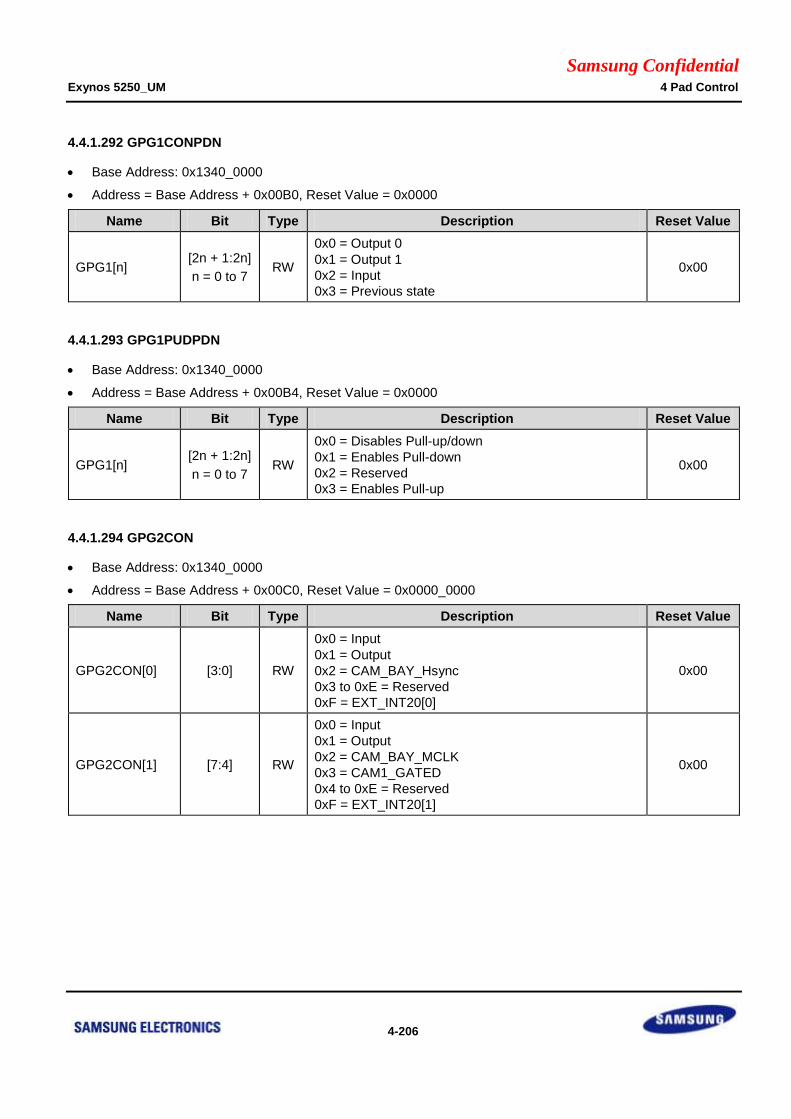
Samsung Confidential Exynos 5250_UM 4 Pad Control
4-206
4.4.1.292 GPG1CONPDN
Base Address: 0x1340_0000
Address = Base Address + 0x00B0, Reset Value = 0x0000
Name Bit Type Description Reset Value
GPG1[n] [2n + 1:2n]
n = 0 to 7 RW
0x0 = Output 0
0x1 = Output 1
0x2 = Input
0x3 = Previous state
0x00
4.4.1.293 GPG1PUDPDN
Base Address: 0x1340_0000
Address = Base Address + 0x00B4, Reset Value = 0x0000
Name Bit Type Description Reset Value
GPG1[n] [2n + 1:2n]
n = 0 to 7 RW
0x0 = Disables Pull-up/down
0x1 = Enables Pull-down
0x2 = Reserved
0x3 = Enables Pull-up
0x00
4.4.1.294 GPG2CON
Base Address: 0x1340_0000
Address = Base Address + 0x00C0, Reset Value = 0x0000_0000
Name Bit Type Description Reset Value
GPG2CON[0] [3:0] RW
0x0 = Input
0x1 = Output
0x2 = CAM_BAY_Hsync
0x3 to 0xE = Reserved
0xF = EXT_INT20[0]
0x00
GPG2CON[1] [7:4] RW
0x0 = Input
0x1 = Output
0x2 = CAM_BAY_MCLK
0x3 = CAM1_GATED
0x4 to 0xE = Reserved
0xF = EXT_INT20[1]
0x00

Samsung Confidential Exynos 5250_UM 4 Pad Control
4-207
4.4.1.295 GPG2DAT
Base Address: 0x1340_0000
Address = Base Address + 0x00C4, Reset Value = 0x00
Name Bit Type Description Reset Value
GPG2DAT[1:0] [1:0] RWX
When you configure the port as input port, the
corresponding bit is the pin state. When you configure
the port as output port, the pin state is the same as the
corresponding bit. When you configure the port as
functional pin, the undefined value will be read.
0x00
4.4.1.296 GPG2PUD
Base Address: 0x1340_0000
Address = Base Address + 0x00C8, Reset Value = 0x0005
Name Bit Type Description Reset Value
GPG2PUD[n] [2n + 1:2n]
n = 0 to 1 RW
0x0 = Disables Pull-up/down
0x1 = Enables Pull-down
0x2 = Reserved
0x3 = Enables Pull-up
0x0005
4.4.1.297 GPG2DRV
Base Address: 0x1340_0000
Address = Base Address + 0x00CC, Reset Value = 0x00_0000
Name Bit Type Description Reset Value
GPG2DRV[n]
[2n + 1:2n]
n = 0 to 1 RW
0x0 = 1x
0x2 = 2x
0x1 = 3x
0x3 = 4x
0x00_0000
[n + 16:16]
n = 0 to 1 RW Reserved. Should be zero. 0x00_0000

Samsung Confidential Exynos 5250_UM 4 Pad Control
4-208
4.4.1.298 GPG2CONPDN
Base Address: 0x1340_0000
Address = Base Address + 0x00D0, Reset Value = 0x0000
Name Bit Type Description Reset Value
GPG2[n] [2n + 1:2n]
n = 0 to 1 RW
0x0 = Output 0,
0x1 = Output 1
0x2 = Input
0x3 = Previous state
0x00
4.4.1.299 GPG2PUDPDN
Base Address: 0x1340_0000
Address = Base Address + 0x00D4, Reset Value = 0x0000
Name Bit Type Description Reset Value
GPG2[n] [2n + 1:2n]
n = 0 to 1 RW
0x0 = Disables Pull-up/down
0x1 = Enables Pull-down
0x2 = Reserved
0x3 = Enables Pull-up
0x00
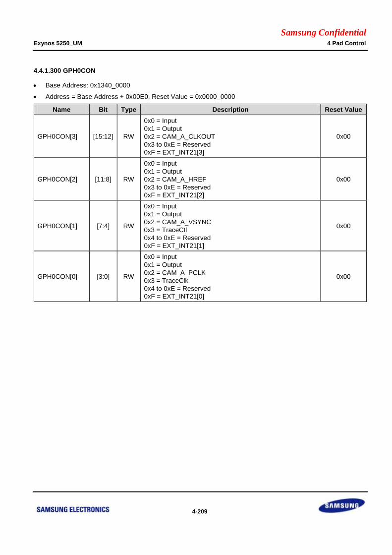
Samsung Confidential Exynos 5250_UM 4 Pad Control
4-209
4.4.1.300 GPH0CON
Base Address: 0x1340_0000
Address = Base Address + 0x00E0, Reset Value = 0x0000_0000
Name Bit Type Description Reset Value
GPH0CON[3] [15:12] RW
0x0 = Input
0x1 = Output
0x2 = CAM_A_CLKOUT
0x3 to 0xE = Reserved
0xF = EXT_INT21[3]
0x00
GPH0CON[2] [11:8] RW
0x0 = Input
0x1 = Output
0x2 = CAM_A_HREF
0x3 to 0xE = Reserved
0xF = EXT_INT21[2]
0x00
GPH0CON[1] [7:4] RW
0x0 = Input
0x1 = Output
0x2 = CAM_A_VSYNC
0x3 = TraceCtl
0x4 to 0xE = Reserved
0xF = EXT_INT21[1]
0x00
GPH0CON[0] [3:0] RW
0x0 = Input
0x1 = Output
0x2 = CAM_A_PCLK
0x3 = TraceClk
0x4 to 0xE = Reserved
0xF = EXT_INT21[0]
0x00

Samsung Confidential Exynos 5250_UM 4 Pad Control
4-210
4.4.1.301 GPH0DAT
Base Address: 0x1340_0000
Address = Base Address + 0x00E4, Reset Value = 0x00
Name Bit Type Description Reset Value
GPH0DAT[3:0] [3:0] RWX
When you configure the port as input port, the
corresponding bit is the pin state. When you configure
the port as output port, the pin state is the same as the
corresponding bit. When you configure the port as
functional pin, the undefined value will be read.
0x00
4.4.1.302 GPH0PUD
Base Address: 0x1340_0000
Address = Base Address + 0x00E8, Reset Value = 0x0055
Name Bit Type Description Reset Value
GPH0PUD[n] [2n + 1:2n]
n = 0 to 3 RW
0x0 = Disables Pull-up/down
0x1 = Enables Pull-down
0x2 = Reserved
0x3 = Enables Pull-up
0x0055
4.4.1.303 GPH0DRV
Base Address: 0x1340_0000
Address = Base Address + 0x00EC, Reset Value = 0x00_0000
Name Bit Type Description Reset Value
GPH0DRV[n]
[2n + 1:2n]
n = 0 to 3 RW
0x0 = 1x
0x2 = 2x
0x1 = 3x
0x3 = 4x
0x00_0000
[n + 16:16]
n = 0 to 3 RW Reserved. Should be zero. 0x00_0000

Samsung Confidential Exynos 5250_UM 4 Pad Control
4-211
4.4.1.304 GPH0CONPDN
Base Address: 0x1340_0000
Address = Base Address + 0x00F0, Reset Value = 0x0000
Name Bit Type Description Reset Value
GPH0[n] [2n + 1:2n]
n = 0 to 3 RW
0x0 = Output 0
0x1 = Output 1
0x2 = Input
0x3 = Previous state
0x00
4.4.1.305 GPH0PUDPDN
Base Address: 0x1340_0000
Address = Base Address + 0x00F4, Reset Value = 0x0000
Name Bit Type Description Reset Value
GPH0[n] [2n + 1:2n]
n = 0 to 3 RW
0x0 = Disables Pull-up/down
0x1 = Enables Pull-down
0x2 = Reserved
0x3 = Enables Pull-up
0x00
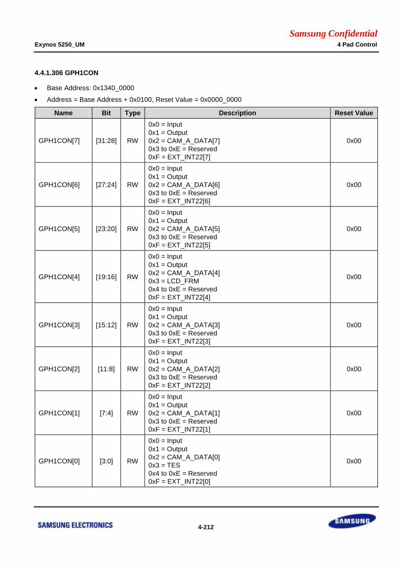
Samsung Confidential Exynos 5250_UM 4 Pad Control
4-212
4.4.1.306 GPH1CON
Base Address: 0x1340_0000
Address = Base Address + 0x0100, Reset Value = 0x0000_0000
Name Bit Type Description Reset Value
GPH1CON[7] [31:28] RW
0x0 = Input
0x1 = Output
0x2 = CAM_A_DATA[7]
0x3 to 0xE = Reserved
0xF = EXT_INT22[7]
0x00
GPH1CON[6] [27:24] RW
0x0 = Input
0x1 = Output
0x2 = CAM_A_DATA[6]
0x3 to 0xE = Reserved
0xF = EXT_INT22[6]
0x00
GPH1CON[5] [23:20] RW
0x0 = Input
0x1 = Output
0x2 = CAM_A_DATA[5]
0x3 to 0xE = Reserved
0xF = EXT_INT22[5]
0x00
GPH1CON[4] [19:16] RW
0x0 = Input
0x1 = Output
0x2 = CAM_A_DATA[4]
0x3 = LCD_FRM
0x4 to 0xE = Reserved
0xF = EXT_INT22[4]
0x00
GPH1CON[3] [15:12] RW
0x0 = Input
0x1 = Output
0x2 = CAM_A_DATA[3]
0x3 to 0xE = Reserved
0xF = EXT_INT22[3]
0x00
GPH1CON[2] [11:8] RW
0x0 = Input
0x1 = Output
0x2 = CAM_A_DATA[2]
0x3 to 0xE = Reserved
0xF = EXT_INT22[2]
0x00
GPH1CON[1] [7:4] RW
0x0 = Input
0x1 = Output
0x2 = CAM_A_DATA[1]
0x3 to 0xE = Reserved
0xF = EXT_INT22[1]
0x00
GPH1CON[0] [3:0] RW
0x0 = Input
0x1 = Output
0x2 = CAM_A_DATA[0]
0x3 = TES
0x4 to 0xE = Reserved
0xF = EXT_INT22[0]
0x00

Samsung Confidential Exynos 5250_UM 4 Pad Control
4-213
4.4.1.307 GPH1DAT
Base Address: 0x1340_0000
Address = Base Address + 0x0104, Reset Value = 0x00
Name Bit Type Description Reset Value
GPH1DAT[7:0] [7:0] RWX
When you configure the port as input port, the
corresponding bit is the pin state. When you configure
the port as output port, the pin state is the same as the
corresponding bit. When you configure the port as
functional pin, the undefined value will be read.
0x00
4.4.1.308 GPH1PUD
Base Address: 0x1340_0000
Address = Base Address + 0x0108, Reset Value = 0x5555
Name Bit Type Description Reset Value
GPH1PUD[n] [2n + 1:2n]
n = 0 to 7 RW
0x0 = Disables Pull-up/down
0x1 = Enables Pull-down
0x2 = Reserved
0x3 = Enables Pull-up
0x5555
4.4.1.309 GPH1DRV
Base Address: 0x1340_0000
Address = Base Address + 0x010C, Reset Value = 0x00_0000
Name Bit Type Description Reset Value
GPH1DRV[n]
[2n + 1:2n]
n = 0 to 7 RW
0x0 = 1x
0x2 = 2x
0x1 = 3x
0x3 = 4x
0x00_0000
[n + 16:16]
n = 0 to 7 RW Reserved. Should be zero. 0x00_0000

Samsung Confidential Exynos 5250_UM 4 Pad Control
4-214
4.4.1.310 GPH1CONPDN
Base Address: 0x1340_0000
Address = Base Address + 0x0110, Reset Value = 0x0000
Name Bit Type Description Reset Value
GPH1[n] [2n + 1:2n]
n = 0 to 7 RW
0x0 = Output 0
0x1 = Output 1
0x2 = Input
0x3 = Previous state
0x00
4.4.1.311 GPH1PUDPDN
Base Address: 0x1340_0000
Address = Base Address + 0x0114, Reset Value = 0x0000
Name Bit Type Description Reset Value
GPH1[n] [2n + 1:2n]
n = 0 to 7 RW
0x0 = Disables Pull-up/down
0x1 = Enables Pull-down
0x2 = Reserved
0x3 = Enables Pull-up
0x00

Samsung Confidential Exynos 5250_UM 4 Pad Control
4-215
4.4.1.312 EXT_INT14CON
Base Address: 0x1340_0000
Address = Base Address + 0x0700, Reset Value = 0x0000_0000
Name Bit Type Description Reset Value
RSVD [31] – Reserved 0x0
EXT_INT14
_CON[7] [30:28] RW
Setting the signaling method of EXT_INT14[7]
0x0 = Sets Low level
0x1 = Sets High level
0x2 = Triggers Falling edge
0x3 = Triggers Rising edge
0x4 = Triggers Both edge
0x5 to 0x7 = Reserved
0x0
RSVD [27] – Reserved 0x0
EXT_INT14
_CON[6] [26:24] RW
Setting the signaling method of EXT_INT14[6]
0x0 = Sets Low level
0x1 = Sets High level
0x2 = Triggers Falling edge
0x3 = Triggers Rising edge
0x4 = Triggers Both edge
0x5 to 0x7 = Reserved
0x0
RSVD [23] – Reserved 0x0
EXT_INT14
_CON[5] [22:20] RW
Setting the signaling method of EXT_INT14[5]
0x0 = Sets Low level
0x1 = Sets High level
0x2 = Triggers Falling edge
0x3 = Triggers Rising edge
0x4 = Triggers Both edge
0x5 to 0x7 = Reserved
0x0
RSVD [19] – Reserved 0x0
EXT_INT14
_CON[4] [18:16] RW
Setting the signaling method of EXT_INT14[4]
0x0 = Sets Low level
0x1 = Sets High level
0x2 = Triggers Falling edge
0x3 = Triggers Rising edge
0x4 = Triggers Both edge
0x5 to 0x7 = Reserved
0x0
RSVD [15] – Reserved 0x0
EXT_INT14
_CON[3] [14:12] RW
Setting the signaling method of EXT_INT14[3]
0x0 = Sets Low level
0x1 = Sets High level
0x2 = Triggers Falling edge
0x3 = Triggers Rising edge
0x4 = Triggers Both edge
0x5 to 0x7 = Reserved
0x0
RSVD [11] – Reserved 0x0
EXT_INT14 [10:8] RW Setting the signaling method of EXT_INT14[2] 0x0

Samsung Confidential Exynos 5250_UM 4 Pad Control
4-216
Name Bit Type Description Reset Value
_CON[2] 0x0 = Sets Low level
0x1 = Sets High level
0x2 = Triggers Falling edge
0x3 = Triggers Rising edge
0x4 = Triggers Both edge
0x5 to 0x7 = Reserved
RSVD [7] – Reserved 0x0
EXT_INT14
_CON[1] [6:4] RW
Setting the signaling method of EXT_INT14[1]
0x0 = Sets Low level
0x1 = Sets High level
0x2 = Triggers Falling edge
0x3 = Triggers Rising edge
0x4 = Triggers Both edge
0x5 to 0x7 = Reserved
0x0
RSVD [3] – Reserved 0x0
EXT_INT14
_CON[0] [2:0] RW
Setting the signaling method of EXT_INT14[0]
0x0 = Sets Low level
0x1 = Sets High level
0x2 = Triggers Falling edge
0x3 = Triggers Rising edge
0x4 = Triggers Both edge
0x5 to 0x7 = Reserved
0x0
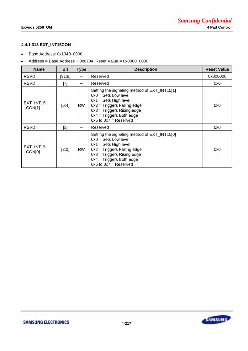
Samsung Confidential Exynos 5250_UM 4 Pad Control
4-217
4.4.1.313 EXT_INT15CON
Base Address: 0x1340_0000
Address = Base Address + 0x0704, Reset Value = 0x0000_0000
Name Bit Type Description Reset Value
RSVD [31:8] – Reserved 0x000000
RSVD [7] – Reserved 0x0
EXT_INT15
_CON[1] [6:4] RW
Setting the signaling method of EXT_INT15[1]
0x0 = Sets Low level
0x1 = Sets High level
0x2 = Triggers Falling edge
0x3 = Triggers Rising edge
0x4 = Triggers Both edge
0x5 to 0x7 = Reserved
0x0
RSVD [3] – Reserved 0x0
EXT_INT15
_CON[0] [2:0] RW
Setting the signaling method of EXT_INT15[0]
0x0 = Sets Low level
0x1 = Sets High level
0x2 = Triggers Falling edge
0x3 = Triggers Rising edge
0x4 = Triggers Both edge
0x5 to 0x7 = Reserved
0x0

Samsung Confidential Exynos 5250_UM 4 Pad Control
4-218
4.4.1.314 EXT_INT16CON
Base Address: 0x1340_0000
Address = Base Address + 0x0708, Reset Value = 0x0000_0000
Name Bit Type Description Reset Value
RSVD [31:16] – Reserved 0x0000
RSVD [15] – Reserved 0x0
EXT_INT16
_CON[3] [14:12] RW
Setting the signaling method of EXT_INT16[3]
0x0 = Sets Low level
0x1 = Sets High level
0x2 = Triggers Falling edge
0x3 = Triggers Rising edge
0x4 = Triggers Both edge
0x5 to 0x7 = Reserved
0x0
RSVD [11] – Reserved 0x0
EXT_INT16
_CON[2] [10:8] RW
Setting the signaling method of EXT_INT16[2]
0x0 = Sets Low level
0x1 = Sets High level
0x2 = Triggers Falling edge
0x3 = Triggers Rising edge
0x4 = Triggers Both edge
0x5 to 0x7 = Reserved
0x0
RSVD [7] – Reserved 0x0
EXT_INT16
_CON[1] [6:4] RW
Setting the signaling method of EXT_INT16[1]
0x0 = Sets Low level
0x1 = Sets High level
0x2 = Triggers Falling edge
0x3 = Triggers Rising edge
0x4 = Triggers Both edge
0x5 to 0x7 = Reserved
0x0
RSVD [3] – Reserved 0x0
EXT_INT16
_CON[0] [2:0] RW
Setting the signaling method of EXT_INT16[0]
0x0 = Sets Low level
0x1 = Sets High level
0x2 = Triggers Falling edge
0x3 = Triggers Rising edge
0x4 = Triggers Both edge
0x5 to 0x7 = Reserved
0x0

Samsung Confidential Exynos 5250_UM 4 Pad Control
4-219
4.4.1.315 EXT_INT17CON
Base Address: 0x1340_0000
Address = Base Address + 0x070C, Reset Value = 0x0000_0000
Name Bit Type Description Reset Value
RSVD [31:16] – Reserved 0x0000
RSVD [15] – Reserved 0x0
EXT_INT17
_CON[3] [14:12] RW
Setting the signaling method of EXT_INT17[3]
0x0 = Sets Low level
0x1 = Sets High level
0x2 = Triggers Falling edge
0x3 = Triggers Rising edge
0x4 = Triggers Both edge
0x5 to 0x7 = Reserved
0x0
RSVD [11] – Reserved 0x0
EXT_INT17
_CON[2] [10:8] RW
Setting the signaling method of EXT_INT17[2]
0x0 = Sets Low level
0x1 = Sets High level
0x2 = Triggers Falling edge
0x3 = Triggers Rising edge
0x4 = Triggers Both edge
0x5 to 0x7 = Reserved
0x0
RSVD [7] – Reserved 0x0
EXT_INT17
_CON[1] [6:4] RW
Setting the signaling method of EXT_INT17[1]
0x0 = Sets Low level
0x1 = Sets High level
0x2 = Triggers Falling edge
0x3 = Triggers Rising edge
0x4 = Triggers Both edge
0x5 to 0x7 = Reserved
0x0
RSVD [3] – Reserved 0x0
EXT_INT17
_CON[0] [2:0] RW
Setting the signaling method of EXT_INT17[0]
0x0 = Sets Low level
0x1 = Sets High level
0x2 = Triggers Falling edge
0x3 = Triggers Rising edge
0x4 = Triggers Both edge
0x5 to 0x7 = Reserved
0x0

Samsung Confidential Exynos 5250_UM 4 Pad Control
4-220
4.4.1.316 EXT_INT18CON
Base Address: 0x1340_0000
Address = Base Address + 0x0710, Reset Value = 0x0000_0000
Name Bit Type Description Reset Value
RSVD [31] – Reserved 0x0
EXT_INT18
_CON[7] [30:28] RW
Setting the signaling method of EXT_INT18[7]
0x0 = Sets Low level
0x1 = Sets High level
0x2 = Triggers Falling edge
0x3 = Triggers Rising edge
0x4 = Triggers Both edge
0x5 to 0x7 = Reserved
0x0
RSVD [27] – Reserved 0x0
EXT_INT18
_CON[6] [26:24] RW
Setting the signaling method of EXT_INT18[6]
0x0 = Sets Low level
0x1 = Sets High level
0x2 = Triggers Falling edge
0x3 = Triggers Rising edge
0x4 = Triggers Both edge
0x5 to 0x7 = Reserved
0x0
RSVD [23] – Reserved 0x0
EXT_INT18
_CON[5] [22:20] RW
Setting the signaling method of EXT_INT18[5]
0x0 = Sets Low level
0x1 = Sets High level
0x2 = Triggers Falling edge
0x3 = Triggers Rising edge
0x4 = Triggers Both edge
0x5 to 0x7 = Reserved
0x0
RSVD [19] – Reserved 0x0
EXT_INT18
_CON[4] [18:16] RW
Setting the signaling method of EXT_INT18[4]
0x0 = Sets Low level
0x1 = Sets High level
0x2 = Triggers Falling edge
0x3 = Triggers Rising edge
0x4 = Triggers Both edge
0x5 to 0x7 = Reserved
0x0
RSVD [15] – Reserved 0x0
EXT_INT18
_CON[3] [14:12] RW
Setting the signaling method of EXT_INT18[3]
0x0 = Sets Low level
0x1 = Sets High level
0x2 = Triggers Falling edge
0x3 = Triggers Rising edge
0x4 = Triggers Both edge
0x5 to 0x7 = Reserved
0x0
RSVD [11] – Reserved 0x0
EXT_INT18 [10:8] RW Setting the signaling method of EXT_INT18[2] 0x0

Samsung Confidential Exynos 5250_UM 4 Pad Control
4-221
Name Bit Type Description Reset Value
_CON[2] 0x0 = Sets Low level
0x1 = Sets High level
0x2 = Triggers Falling edge
0x3 = Triggers Rising edge
0x4 = Triggers Both edge
0x5 to 0x7 = Reserved
RSVD [7] – Reserved 0x0
EXT_INT18
_CON[1] [6:4] RW
Setting the signaling method of EXT_INT18[1]
0x0 = Sets Low level
0x1 = Sets High level
0x2 = Triggers Falling edge
0x3 = Triggers Rising edge
0x4 = Triggers Both edge
0x5 to 0x7 = Reserved
0x0
RSVD [3] – Reserved 0x0
EXT_INT18
_CON[0] [2:0] RW
Setting the signaling method of EXT_INT18[0]
0x0 = Sets Low level
0x1 = Sets High level
0x2 = Triggers Falling edge
0x3 = Triggers Rising edge
0x4 = Triggers Both edge
0x5 to 0x7 = Reserved
0x0
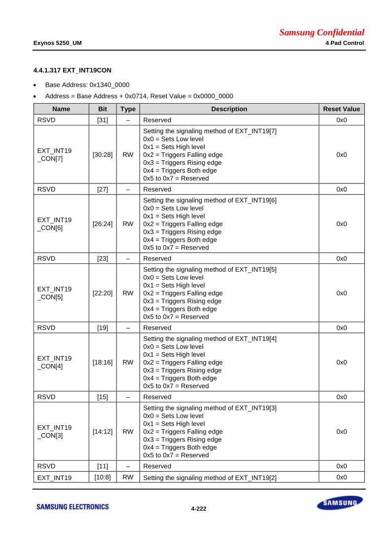
Samsung Confidential Exynos 5250_UM 4 Pad Control
4-222
4.4.1.317 EXT_INT19CON
Base Address: 0x1340_0000
Address = Base Address + 0x0714, Reset Value = 0x0000_0000
Name Bit Type Description Reset Value
RSVD [31] – Reserved 0x0
EXT_INT19
_CON[7] [30:28] RW
Setting the signaling method of EXT_INT19[7]
0x0 = Sets Low level
0x1 = Sets High level
0x2 = Triggers Falling edge
0x3 = Triggers Rising edge
0x4 = Triggers Both edge
0x5 to 0x7 = Reserved
0x0
RSVD [27] – Reserved 0x0
EXT_INT19
_CON[6] [26:24] RW
Setting the signaling method of EXT_INT19[6]
0x0 = Sets Low level
0x1 = Sets High level
0x2 = Triggers Falling edge
0x3 = Triggers Rising edge
0x4 = Triggers Both edge
0x5 to 0x7 = Reserved
0x0
RSVD [23] – Reserved 0x0
EXT_INT19
_CON[5] [22:20] RW
Setting the signaling method of EXT_INT19[5]
0x0 = Sets Low level
0x1 = Sets High level
0x2 = Triggers Falling edge
0x3 = Triggers Rising edge
0x4 = Triggers Both edge
0x5 to 0x7 = Reserved
0x0
RSVD [19] – Reserved 0x0
EXT_INT19
_CON[4] [18:16] RW
Setting the signaling method of EXT_INT19[4]
0x0 = Sets Low level
0x1 = Sets High level
0x2 = Triggers Falling edge
0x3 = Triggers Rising edge
0x4 = Triggers Both edge
0x5 to 0x7 = Reserved
0x0
RSVD [15] – Reserved 0x0
EXT_INT19
_CON[3] [14:12] RW
Setting the signaling method of EXT_INT19[3]
0x0 = Sets Low level
0x1 = Sets High level
0x2 = Triggers Falling edge
0x3 = Triggers Rising edge
0x4 = Triggers Both edge
0x5 to 0x7 = Reserved
0x0
RSVD [11] – Reserved 0x0
EXT_INT19 [10:8] RW Setting the signaling method of EXT_INT19[2] 0x0

Samsung Confidential Exynos 5250_UM 4 Pad Control
4-223
Name Bit Type Description Reset Value
_CON[2] 0x0 = Sets Low level
0x1 = Sets High level
0x2 = Triggers Falling edge
0x3 = Triggers Rising edge
0x4 = Triggers Both edge
0x5 to 0x7 = Reserved
RSVD [7] – Reserved 0x0
EXT_INT19
_CON[1] [6:4] RW
Setting the signaling method of EXT_INT19[1]
0x0 = Sets Low level
0x1 = Sets High level
0x2 = Triggers Falling edge
0x3 = Triggers Rising edge
0x4 = Triggers Both edge
0x5 to 0x7 = Reserved
0x0
RSVD [3] – Reserved 0x0
EXT_INT19
_CON[0] [2:0] RW
Setting the signaling method of EXT_INT19[0]
0x0 = Sets Low level
0x1 = Sets High level
0x2 = Triggers Falling edge
0x3 = Triggers Rising edge
0x4 = Triggers Both edge
0x5 to 0x7 = Reserved
0x0

Samsung Confidential Exynos 5250_UM 4 Pad Control
4-224
4.4.1.318 EXT_INT20CON
Base Address: 0x1340_0000
Address = Base Address + 0x0718, Reset Value = 0x0000_0000
Name Bit Type Description Reset Value
RSVD [31:8] – Reserved 0x000000
RSVD [7] – Reserved 0x0
EXT_INT20
_CON[1] [6:4] RW
Setting the signaling method of EXT_INT20[1]
0x0 = Sets Low level
0x1 = Sets High level
0x2 = Triggers Falling edge
0x3 = Triggers Rising edge
0x4 = Triggers Both edge
0x5 to 0x7 = Reserved
0x0
RSVD [3] – Reserved 0x0
EXT_INT20
_CON[0] [2:0] RW
Setting the signaling method of EXT_INT20[0]
0x0 = Sets Low level
0x1 = Sets High level
0x2 = Triggers Falling edge
0x3 = Triggers Rising edge
0x4 = Triggers Both edge
0x5 to 0x7 = Reserved
0x0

Samsung Confidential Exynos 5250_UM 4 Pad Control
4-225
4.4.1.319 EXT_INT21CON
Base Address: 0x1340_0000
Address = Base Address + 0x071C, Reset Value = 0x0000_0000
Name Bit Type Description Reset Value
RSVD [31:16] – Reserved 0x0000
RSVD [15] – Reserved 0x0
EXT_INT21
_CON[3] [14:12] RW
Setting the signaling method of EXT_INT21[3]
0x0 = Sets Low level
0x1 = Sets High level
0x2 = Triggers Falling edge
0x3 = Triggers Rising edge
0x4 = Triggers Both edge
0x5 to 0x7 = Reserved
0x0
RSVD [11] – Reserved 0x0
EXT_INT21
_CON[2] [10:8] RW
Setting the signaling method of EXT_INT21[2]
0x0 = Sets Low level
0x1 = Sets High level
0x2 = Triggers Falling edge
0x3 = Triggers Rising edge
0x4 = Triggers Both edge
0x5 to 0x7 = Reserved
0x0
RSVD [7] – Reserved 0x0
EXT_INT21
_CON[1] [6:4] RW
Setting the signaling method of EXT_INT21[1]
0x0 = Sets Low level
0x1 = Sets High level
0x2 = Triggers Falling edge
0x3 = Triggers Rising edge
0x4 = Triggers Both edge
0x5 to 0x7 = Reserved
0x0
RSVD [3] – Reserved 0x0
EXT_INT21
_CON[0] [2:0] RW
Setting the signaling method of EXT_INT21[0]
0x0 = Sets Low level
0x1 = Sets High level
0x2 = Triggers Falling edge
0x3 = Triggers Rising edge
0x4 = Triggers Both edge
0x5 to 0x7 = Reserved
0x0

Samsung Confidential Exynos 5250_UM 4 Pad Control
4-226
4.4.1.320 EXT_INT22CON
Base Address: 0x1340_0000
Address = Base Address + 0x0720, Reset Value = 0x0000_0000
Name Bit Type Description Reset Value
RSVD [31] – Reserved 0x0
EXT_INT22
_CON[7] [30:28] RW
Setting the signaling method of EXT_INT22[7]
0x0 = Sets Low level
0x1 = Sets High level
0x2 = Triggers Falling edge
0x3 = Triggers Rising edge
0x4 = Triggers Both edge
0x5 to 0x7 = Reserved
0x0
RSVD [27] – Reserved 0x0
EXT_INT22
_CON[6] [26:24] RW
Setting the signaling method of EXT_INT22[6]
0x0 = Sets Low level
0x1 = Sets High level
0x2 = Triggers Falling edge
0x3 = Triggers Rising edge
0x4 = Triggers Both edge
0x5 to 0x7 = Reserved
0x0
RSVD [23] – Reserved 0x0
EXT_INT22
_CON[5] [22:20] RW
Setting the signaling method of EXT_INT22[5]
0x0 = Sets Low level
0x1 = Sets High level
0x2 = Triggers Falling edge
0x3 = Triggers Rising edge
0x4 = Triggers Both edge
0x5 to 0x7 = Reserved
0x0
RSVD [19] – Reserved 0x0
EXT_INT22
_CON[4] [18:16] RW
Setting the signaling method of EXT_INT22[4]
0x0 = Sets Low level
0x1 = Sets High level
0x2 = Triggers Falling edge
0x3 = Triggers Rising edge
0x4 = Triggers Both edge
0x5 to 0x7 = Reserved
0x0
RSVD [15] – Reserved 0x0
EXT_INT22
_CON[3] [14:12] RW
Setting the signaling method of EXT_INT22[3]
0x0 = Sets Low level
0x1 = Sets High level
0x2 = Triggers Falling edge
0x3 = Triggers Rising edge
0x4 = Triggers Both edge
0x5 to 0x7 = Reserved
0x0
RSVD [11] – Reserved 0x0
EXT_INT22 [10:8] RW Setting the signaling method of EXT_INT22[2] 0x0

Samsung Confidential Exynos 5250_UM 4 Pad Control
4-227
Name Bit Type Description Reset Value
_CON[2] 0x0 = Sets Low level
0x1 = Sets High level
0x2 = Triggers Falling edge
0x3 = Triggers Rising edge
0x4 = Triggers Both edge
0x5 to 0x7 = Reserved
RSVD [7] – Reserved 0x0
EXT_INT22
_CON[1] [6:4] RW
Setting the signaling method of EXT_INT22[1]
0x0 = Sets Low level
0x1 = Sets High level
0x2 = Triggers Falling edge
0x3 = Triggers Rising edge
0x4 = Triggers Both edge
0x5 to 0x7 = Reserved
0x0
RSVD [3] – Reserved 0x0
EXT_INT22
_CON[0] [2:0] RW
Setting the signaling method of EXT_INT22[0]
0x0 = Sets Low level
0x1 = Sets High level
0x2 = Triggers Falling edge
0x3 = Triggers Rising edge
0x4 = Triggers Both edge
0x5 to 0x7 = Reserved
0x0

Samsung Confidential Exynos 5250_UM 4 Pad Control
4-228
4.4.1.321 EXT_INT14_FLTCON0
Base Address: 0x1340_0000
Address = Base Address + 0x0800, Reset Value = 0x0000_0000
Name Bit Type Description Reset Value
FLTEN1[3] [31] RW
Enables Filter for EXT_INT14[3]
0x0 = Disables
0x1 = Enables
0x0
FLTWIDTH1[3] [30:24] RW Filtering width of EXT_INT14[3] 0x00
FLTEN1[2] [23] RW
Enables Filter for EXT_INT14[2]
0x0 = Disables
0x1 = Enables
0x0
FLTWIDTH1[2] [22:16] RW Filtering width of EXT_INT14[2] 0x00
FLTEN1[1] [15] RW
Enables Filter for EXT_INT14[1]
0x0 = Disables
0x1 = Enables
0x0
FLTWIDTH1[1] [14:8] RW Filtering width of EXT_INT14[1] 0x00
FLTEN1[0] [7] RW
Enables Filter for EXT_INT14[0]
0x0 = Disables
0x1 = Enables
0x0
FLTWIDTH1[0] [6:0] RW Filtering width of EXT_INT14[0] 0x00

Samsung Confidential Exynos 5250_UM 4 Pad Control
4-229
4.4.1.322 EXT_INT14_FLTCON1
Base Address: 0x1340_0000
Address = Base Address + 0x0804, Reset Value = 0x0000_0000
Name Bit Type Description Reset Value
FLTEN1[7] [31] RW
Enables Filter for EXT_INT14[7]
0x0 = Disables
0x1 = Enables
0x0
FLTWIDTH1[7] [30:24] RW Filtering width of EXT_INT14[7] 0x00
FLTEN1[6] [23] RW
Enables Filter for EXT_INT14[6]
0x0 = Disables
0x1 = Enables
0x0
FLTWIDTH1[6] [22:16] RW Filtering width of EXT_INT14[6] 0x00
FLTEN1[5] [15] RW
Enables Filter for EXT_INT14[5]
0x0 = Disables
0x1 = Enables
0x0
FLTWIDTH1[5] [14:8] RW Filtering width of EXT_INT14[5] 0x00
FLTEN1[4] [7] RW
Enables Filter for EXT_INT14[4]
0x0 = Disables
0x1 = Enables
0x0
FLTWIDTH1[4] [6:0] RW Filtering width of EXT_INT14[4] 0x00
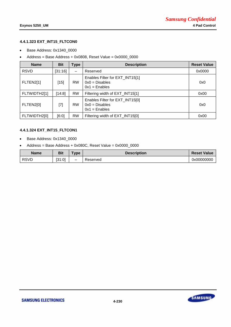
Samsung Confidential Exynos 5250_UM 4 Pad Control
4-230
4.4.1.323 EXT_INT15_FLTCON0
Base Address: 0x1340_0000
Address = Base Address + 0x0808, Reset Value = 0x0000_0000
Name Bit Type Description Reset Value
RSVD [31:16] – Reserved 0x0000
FLTEN2[1] [15] RW
Enables Filter for EXT_INT15[1]
0x0 = Disables
0x1 = Enables
0x0
FLTWIDTH2[1] [14:8] RW Filtering width of EXT_INT15[1] 0x00
FLTEN2[0] [7] RW
Enables Filter for EXT_INT15[0]
0x0 = Disables
0x1 = Enables
0x0
FLTWIDTH2[0] [6:0] RW Filtering width of EXT_INT15[0] 0x00
4.4.1.324 EXT_INT15_FLTCON1
Base Address: 0x1340_0000
Address = Base Address + 0x080C, Reset Value = 0x0000_0000
Name Bit Type Description Reset Value
RSVD [31:0] – Reserved 0x00000000

Samsung Confidential Exynos 5250_UM 4 Pad Control
4-231
4.4.1.325 EXT_INT16_FLTCON0
Base Address: 0x1340_0000
Address = Base Address + 0x0810, Reset Value = 0x0000_0000
Name Bit Type Description Reset Value
FLTEN3[3] [31] RW
Enables Filter for EXT_INT16[3]
0x0 = Disables
0x1 = Enables
0x0
FLTWIDTH3[3] [30:24] RW Filtering width of EXT_INT16[3] 0x00
FLTEN3[2] [23] RW
Enables Filter for EXT_INT16[2]
0x0 = Disables
0x1 = Enables
0x0
FLTWIDTH3[2] [22:16] RW Filtering width of EXT_INT16[2] 0x00
FLTEN3[1] [15] RW
Enables Filter for EXT_INT16[1]
0x0 = Disables
0x1 = Enables
0x0
FLTWIDTH3[1] [14:8] RW Filtering width of EXT_INT16[1] 0x00
FLTEN3[0] [7] RW
Enables Filter for EXT_INT16[0]
0x0 = Disables
0x1 = Enables
0x0
FLTWIDTH3[0] [6:0] RW Filtering width of EXT_INT16[0] 0x00
4.4.1.326 EXT_INT16_FLTCON1
Base Address: 0x1340_0000
Address = Base Address + 0x0814, Reset Value = 0x0000_0000
Name Bit Type Description Reset Value
RSVD [31:0] – Reserved 0x00000000

Samsung Confidential Exynos 5250_UM 4 Pad Control
4-232
4.4.1.327 EXT_INT17_FLTCON0
Base Address: 0x1340_0000
Address = Base Address + 0x0818, Reset Value = 0x0000_0000
Name Bit Type Description Reset Value
FLTEN4[3] [31] RW
Enables Filter for EXT_INT17[3]
0x0 = Disables
0x1 = Enables
0x0
FLTWIDTH4[3] [30:24] RW Filtering width of EXT_INT17[3] 0x00
FLTEN4[2] [23] RW
Enables Filter for EXT_INT17[2]
0x0 = Disables
0x1 = Enables
0x0
FLTWIDTH4[2] [22:16] RW Filtering width of EXT_INT17[2] 0x00
FLTEN4[1] [15] RW
Enables Filter for EXT_INT17[1]
0x0 = Disables
0x1 = Enables
0x0
FLTWIDTH4[1] [14:8] RW Filtering width of EXT_INT17[1] 0x00
FLTEN4[0] [7] RW
Enables Filter for EXT_INT17[0]
0x0 = Disables
0x1 = Enables
0x0
FLTWIDTH4[0] [6:0] RW Filtering width of EXT_INT17[0] 0x00
4.4.1.328 EXT_INT17_FLTCON1
Base Address: 0x1340_0000
Address = Base Address + 0x081C, Reset Value = 0x0000_0000
Name Bit Type Description Reset Value
RSVD [31:0] – Reserved 0x00000000

Samsung Confidential Exynos 5250_UM 4 Pad Control
4-233
4.4.1.329 EXT_INT18_FLTCON0
Base Address: 0x1340_0000
Address = Base Address + 0x0820, Reset Value = 0x0000_0000
Name Bit Type Description Reset Value
FLTEN5[3] [31] RW
Enables Filter for EXT_INT18[3]
0x0 = Disables
0x1 = Enables
0x0
FLTWIDTH5[3] [30:24] RW Filtering width of EXT_INT18[3] 0x00
FLTEN5[2] [23] RW
Enables Filter for EXT_INT18[2]
0x0 = Disables
0x1 = Enables
0x0
FLTWIDTH5[2] [22:16] RW Filtering width of EXT_INT18[2] 0x00
FLTEN5[1] [15] RW
Enables Filter for EXT_INT18[1]
0x0 = Disables
0x1 = Enables
0x0
FLTWIDTH5[1] [14:8] RW Filtering width of EXT_INT18[1] 0x00
FLTEN5[0] [7] RW
Enables Filter for EXT_INT18[0]
0x0 = Disables
0x1 = Enables
0x0
FLTWIDTH5[0] [6:0] RW Filtering width of EXT_INT18[0] 0x00

Samsung Confidential Exynos 5250_UM 4 Pad Control
4-234
4.4.1.330 EXT_INT18_FLTCON1
Base Address: 0x1340_0000
Address = Base Address + 0x0824, Reset Value = 0x0000_0000
Name Bit Type Description Reset Value
FLTEN5[7] [31] RW
Enables Filter for EXT_INT18[7]
0x0 = Disables
0x1 = Enables
0x0
FLTWIDTH5[7] [30:24] RW Filtering width of EXT_INT18[7] 0x00
FLTEN5[6] [23] RW
Enables Filter for EXT_INT18[6]
0x0 = Disables
0x1 = Enables
0x0
FLTWIDTH5[6] [22:16] RW Filtering width of EXT_INT18[6] 0x00
FLTEN5[5] [15] RW
Enables Filter for EXT_INT18[5]
0x0 = Disables
0x1 = Enables
0x0
FLTWIDTH5[5] [14:8] RW Filtering width of EXT_INT18[5] 0x00
FLTEN5[4] [7] RW
Enables Filter for EXT_INT18[4]
0x0 = Disables
0x1 = Enables
0x0
FLTWIDTH5[4] [6:0] RW Filtering width of EXT_INT18[4] 0x00

Samsung Confidential Exynos 5250_UM 4 Pad Control
4-235
4.4.1.331 EXT_INT19_FLTCON0
Base Address: 0x1340_0000
Address = Base Address + 0x0828, Reset Value = 0x0000_0000
Name Bit Type Description Reset Value
FLTEN6[3] [31] RW
Enables Filter for EXT_INT19[3]
0x0 = Disables
0x1 = Enables
0x0
FLTWIDTH6[3] [30:24] RW Filtering width of EXT_INT19[3] 0x00
FLTEN6[2] [23] RW
Enables Filter for EXT_INT19[2]
0x0 = Disables
0x1 = Enables
0x0
FLTWIDTH6[2] [22:16] RW Filtering width of EXT_INT19[2] 0x00
FLTEN6[1] [15] RW
Enables Filter for EXT_INT19[1]
0x0 = Disables
0x1 = Enables
0x0
FLTWIDTH6[1] [14:8] RW Filtering width of EXT_INT19[1] 0x00
FLTEN6[0] [7] RW
Enables Filter for EXT_INT19[0]
0x0 = Disables
0x1 = Enables
0x0
FLTWIDTH6[0] [6:0] RW Filtering width of EXT_INT19[0] 0x00

Samsung Confidential Exynos 5250_UM 4 Pad Control
4-236
4.4.1.332 EXT_INT19_FLTCON1
Base Address: 0x1340_0000
Address = Base Address + 0x082C, Reset Value = 0x0000_0000
Name Bit Type Description Reset Value
FLTEN6[7] [31] RW
Enables Filter for EXT_INT19[7]
0x0 = Disables
0x1 = Enables
0x0
FLTWIDTH6[7] [30:24] RW Filtering width of EXT_INT19[7] 0x00
FLTEN6[6] [23] RW
Enables Filter for EXT_INT19[6]
0x0 = Disables
0x1 = Enables
0x0
FLTWIDTH6[6] [22:16] RW Filtering width of EXT_INT19[6] 0x00
FLTEN6[5] [15] RW
Enables Filter for EXT_INT19[5]
0x0 = Disables
0x1 = Enables
0x0
FLTWIDTH6[5] [14:8] RW Filtering width of EXT_INT19[5] 0x00
FLTEN6[4] [7] RW
Enables Filter for EXT_INT19[4]
0x0 = Disables
0x1 = Enables
0x0
FLTWIDTH6[4] [6:0] RW Filtering width of EXT_INT19[4] 0x00

Samsung Confidential Exynos 5250_UM 4 Pad Control
4-237
4.4.1.333 EXT_INT20_FLTCON0
Base Address: 0x1340_0000
Address = Base Address + 0x0830, Reset Value = 0x0000_0000
Name Bit Type Description Reset Value
RSVD [31:16] – Reserved 0x0000
FLTEN7[1] [15] RW
Enables Filter for EXT_INT20[1]
0x0 = Disables
0x1 = Enables
0x0
FLTWIDTH7[1] [14:8] RW Filtering width of EXT_INT20[1] 0x00
FLTEN7[0] [7] RW
Enables Filter for EXT_INT20[0]
0x0 = Disables
0x1 = Enables
0x0
FLTWIDTH7[0] [6:0] RW Filtering width of EXT_INT20[0] 0x00
4.4.1.334 EXT_INT20_FLTCON1
Base Address: 0x1340_0000
Address = Base Address + 0x0834, Reset Value = 0x0000_0000
Name Bit Type Description Reset Value
RSVD [31:0] – Reserved 0x00000000
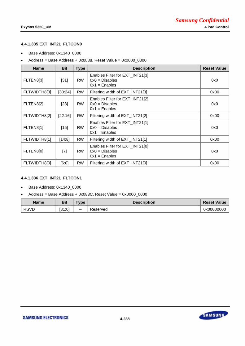
Samsung Confidential Exynos 5250_UM 4 Pad Control
4-238
4.4.1.335 EXT_INT21_FLTCON0
Base Address: 0x1340_0000
Address = Base Address + 0x0838, Reset Value = 0x0000_0000
Name Bit Type Description Reset Value
FLTEN8[3] [31] RW
Enables Filter for EXT_INT21[3]
0x0 = Disables
0x1 = Enables
0x0
FLTWIDTH8[3] [30:24] RW Filtering width of EXT_INT21[3] 0x00
FLTEN8[2] [23] RW
Enables Filter for EXT_INT21[2]
0x0 = Disables
0x1 = Enables
0x0
FLTWIDTH8[2] [22:16] RW Filtering width of EXT_INT21[2] 0x00
FLTEN8[1] [15] RW
Enables Filter for EXT_INT21[1]
0x0 = Disables
0x1 = Enables
0x0
FLTWIDTH8[1] [14:8] RW Filtering width of EXT_INT21[1] 0x00
FLTEN8[0] [7] RW
Enables Filter for EXT_INT21[0]
0x0 = Disables
0x1 = Enables
0x0
FLTWIDTH8[0] [6:0] RW Filtering width of EXT_INT21[0] 0x00
4.4.1.336 EXT_INT21_FLTCON1
Base Address: 0x1340_0000
Address = Base Address + 0x083C, Reset Value = 0x0000_0000
Name Bit Type Description Reset Value
RSVD [31:0] – Reserved 0x00000000

Samsung Confidential Exynos 5250_UM 4 Pad Control
4-239
4.4.1.337 EXT_INT22_FLTCON0
Base Address: 0x1340_0000
Address = Base Address + 0x0840, Reset Value = 0x0000_0000
Name Bit Type Description Reset Value
FLTEN9[3] [31] RW
Enables Filter for EXT_INT22[3]
0x0 = Disables
0x1 = Enables
0x0
FLTWIDTH9[3] [30:24] RW Filtering width of EXT_INT22[3] 0x00
FLTEN9[2] [23] RW
Enables Filter for EXT_INT22[2]
0x0 = Disables
0x1 = Enables
0x0
FLTWIDTH9[2] [22:16] RW Filtering width of EXT_INT22[2] 0x00
FLTEN9[1] [15] RW
Enables Filter for EXT_INT22[1]
0x0 = Disables
0x1 = Enables
0x0
FLTWIDTH9[1] [14:8] RW Filtering width of EXT_INT22[1] 0x00
FLTEN9[0] [7] RW
Enables Filter for EXT_INT22[0]
0x0 = Disables
0x1 = Enables
0x0
FLTWIDTH9[0] [6:0] RW Filtering width of EXT_INT22[0] 0x00

Samsung Confidential Exynos 5250_UM 4 Pad Control
4-240
4.4.1.338 EXT_INT22_FLTCON1
Base Address: 0x1340_0000
Address = Base Address + 0x0844, Reset Value = 0x0000_0000
Name Bit Type Description Reset Value
FLTEN9[7] [31] RW
Enables Filter for EXT_INT22[7]
0x0 = Disables
0x1 = Enables
0x0
FLTWIDTH9[7] [30:24] RW Filtering width of EXT_INT22[7] 0x00
FLTEN9[6] [23] RW
Enables Filter for EXT_INT22[6]
0x0 = Disables
0x1 = Enables
0x0
FLTWIDTH9[6] [22:16] RW Filtering width of EXT_INT22[6] 0x00
FLTEN9[5] [15] RW
Enables Filter for EXT_INT22[5]
0x0 = Disables
0x1 = Enables
0x0
FLTWIDTH9[5] [14:8] RW Filtering width of EXT_INT22[5] 0x00
FLTEN9[4] [7] RW
Enables Filter for EXT_INT22[4]
0x0 = Disables
0x1 = Enables
0x0
FLTWIDTH9[4] [6:0] RW Filtering width of EXT_INT22[4] 0x00

Samsung Confidential Exynos 5250_UM 4 Pad Control
4-241
4.4.1.339 EXT_INT14_MASK
Base Address: 0x1340_0000
Address = Base Address + 0x0900, Reset Value = 0x0000_00FF
Name Bit Type Description Reset Value
RSVD [31:8] – Reserved 0x000000
EXT_INT14
_MASK[7] [7] RW
0x0 = Enables Interrupt
0x1 = Masks Interrupt 0x1
EXT_INT14
_MASK[6] [6] RW
0x0 = Enables Interrupt
0x1 = Masked 0x1
EXT_INT14
_MASK[5] [5] RW
0x0 = Enables Interrupt
0x1 = Masks Interrupt 0x1
EXT_INT14
_MASK[4] [4] RW
0x0 = Enables Interrupt
0x1 = Masks Interrupt 0x1
EXT_INT14
_MASK[3] [3] RW
0x0 = Enables Interrupt
0x1 = Masks Interrupt 0x1
EXT_INT14
_MASK[2] [2] RW
0x0 = Enables Interrupt
0x1 = Masks Interrupt 0x1
EXT_INT14
_MASK[1] [1] RW
0x0 = Enables Interrupt
0x1 = Masks Interrupt 0x1
EXT_INT14
_MASK[0] [0] RW
0x0 = Enables Interrupt
0x1 = Masks Interrupt 0x1
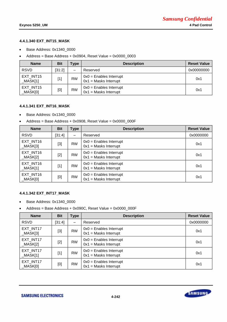
Samsung Confidential Exynos 5250_UM 4 Pad Control
4-242
4.4.1.340 EXT_INT15_MASK
Base Address: 0x1340_0000
Address = Base Address + 0x0904, Reset Value = 0x0000_0003
Name Bit Type Description Reset Value
RSVD [31:2] – Reserved 0x00000000
EXT_INT15
_MASK[1] [1] RW
0x0 = Enables Interrupt
0x1 = Masks Interrupt 0x1
EXT_INT15
_MASK[0] [0] RW
0x0 = Enables Interrupt
0x1 = Masks Interrupt 0x1
4.4.1.341 EXT_INT16_MASK
Base Address: 0x1340_0000
Address = Base Address + 0x0908, Reset Value = 0x0000_000F
Name Bit Type Description Reset Value
RSVD [31:4] – Reserved 0x0000000
EXT_INT16
_MASK[3] [3] RW
0x0 = Enables Interrupt
0x1 = Masks Interrupt 0x1
EXT_INT16
_MASK[2] [2] RW
0x0 = Enables Interrupt
0x1 = Masks Interrupt 0x1
EXT_INT16
_MASK[1] [1] RW
0x0 = Enables Interrupt
0x1 = Masks Interrupt 0x1
EXT_INT16
_MASK[0] [0] RW
0x0 = Enables Interrupt
0x1 = Masks Interrupt 0x1
4.4.1.342 EXT_INT17_MASK
Base Address: 0x1340_0000
Address = Base Address + 0x090C, Reset Value = 0x0000_000F
Name Bit Type Description Reset Value
RSVD [31:4] – Reserved 0x0000000
EXT_INT17
_MASK[3] [3] RW
0x0 = Enables Interrupt
0x1 = Masks Interrupt 0x1
EXT_INT17
_MASK[2] [2] RW
0x0 = Enables Interrupt
0x1 = Masks Interrupt 0x1
EXT_INT17
_MASK[1] [1] RW
0x0 = Enables Interrupt
0x1 = Masks Interrupt 0x1
EXT_INT17
_MASK[0] [0] RW
0x0 = Enables Interrupt
0x1 = Masks Interrupt 0x1

Samsung Confidential Exynos 5250_UM 4 Pad Control
4-243
4.4.1.343 EXT_INT18_MASK
Base Address: 0x1340_0000
Address = Base Address + 0x0910, Reset Value = 0x0000_00FF
Name Bit Type Description Reset Value
RSVD [31:8] – Reserved 0x000000
EXT_INT18
_MASK[7] [7] RW
0x0 = Enables Interrupt
0x1 = Masks Interrupt 0x1
EXT_INT18
_MASK[6] [6] RW
0x0 = Enables Interrupt
0x1 = Masks Interrupt 0x1
EXT_INT18
_MASK[5] [5] RW
0x0 = Enables Interrupt
0x1 = Masks Interrupt 0x1
EXT_INT18
_MASK[4] [4] RW
0x0 = Enables Interrupt
0x1 = Masks Interrupt 0x1
EXT_INT18
_MASK[3] [3] RW
0x0 = Enables Interrupt
0x1 = Masks Interrupt 0x1
EXT_INT18
_MASK[2] [2] RW
0x0 = Enables Interrupt
0x1 = Masks Interrupt 0x1
EXT_INT18
_MASK[1] [1] RW
0x0 = Enables Interrupt
0x1 = Masks Interrupt 0x1
EXT_INT18
_MASK[0] [0] RW
0x0 = Enables Interrupt
0x1 = Masks Interrupt 0x1

Samsung Confidential Exynos 5250_UM 4 Pad Control
4-244
4.4.1.344 EXT_INT19_MASK
Base Address: 0x1340_0000
Address = Base Address + 0x0914, Reset Value = 0x0000_00FF
Name Bit Type Description Reset Value
RSVD [31:8] – Reserved 0x000000
EXT_INT19
_MASK[7] [7] RW
0x0 = Enables Interrupt
0x1 = Masks Interrupt 0x1
EXT_INT19
_MASK[6] [6] RW
0x0 = Enables Interrupt
0x1 = Masks Interrupt 0x1
EXT_INT19
_MASK[5] [5] RW
0x0 = Enables Interrupt
0x1 = Masks Interrupt 0x1
EXT_INT19
_MASK[4] [4] RW
0x0 = Enable Interrupt
0x1 = Masks Interrupt 0x1
EXT_INT19
_MASK[3] [3] RW
0x0 = Enables Interrupt
0x1 = Masks Interrupt 0x1
EXT_INT19
_MASK[2] [2] RW
0x0 = Enables Interrupt
0x1 = Masks Interrupt 0x1
EXT_INT19
_MASK[1] [1] RW
0x0 = Enables Interrupt
0x1 = Masks Interrupt 0x1
EXT_INT19
_MASK[0] [0] RW
0x0 = Enables Interrupt
0x1 = Masks Interrupt 0x1
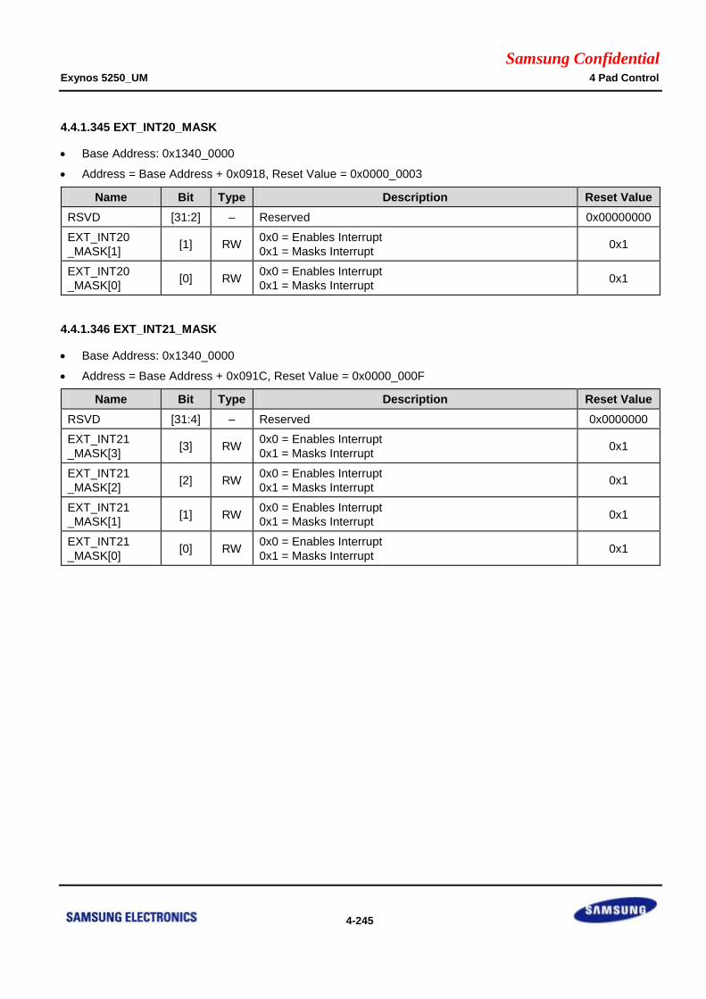
Samsung Confidential Exynos 5250_UM 4 Pad Control
4-245
4.4.1.345 EXT_INT20_MASK
Base Address: 0x1340_0000
Address = Base Address + 0x0918, Reset Value = 0x0000_0003
Name Bit Type Description Reset Value
RSVD [31:2] – Reserved 0x00000000
EXT_INT20
_MASK[1] [1] RW
0x0 = Enables Interrupt
0x1 = Masks Interrupt 0x1
EXT_INT20
_MASK[0] [0] RW
0x0 = Enables Interrupt
0x1 = Masks Interrupt 0x1
4.4.1.346 EXT_INT21_MASK
Base Address: 0x1340_0000
Address = Base Address + 0x091C, Reset Value = 0x0000_000F
Name Bit Type Description Reset Value
RSVD [31:4] – Reserved 0x0000000
EXT_INT21
_MASK[3] [3] RW
0x0 = Enables Interrupt
0x1 = Masks Interrupt 0x1
EXT_INT21
_MASK[2] [2] RW
0x0 = Enables Interrupt
0x1 = Masks Interrupt 0x1
EXT_INT21
_MASK[1] [1] RW
0x0 = Enables Interrupt
0x1 = Masks Interrupt 0x1
EXT_INT21
_MASK[0] [0] RW
0x0 = Enables Interrupt
0x1 = Masks Interrupt 0x1

Samsung Confidential Exynos 5250_UM 4 Pad Control
4-246
4.4.1.347 EXT_INT22_MASK
Base Address: 0x1340_0000
Address = Base Address + 0x0920, Reset Value = 0x0000_00FF
Name Bit Type Description Reset Value
RSVD [31:8] – Reserved 0x000000
EXT_INT22
_MASK[7] [7] RW
0x0 = Enables Interrupt
0x1 = Masks Interrupt 0x1
EXT_INT22
_MASK[6] [6] RW
0x0 = Enables Interrupt
0x1 = Masks Interrupt 0x1
EXT_INT22
_MASK[5] [5] RW
0x0 = Enables Interrupt
0x1 = Masks Interrupt 0x1
EXT_INT22
_MASK[4] [4] RW
0x0 = Enables Interrupt
0x1 = Masks Interrupt 0x1
EXT_INT22
_MASK[3] [3] RW
0x0 = Enables Interrupt
0x1 = Masks Interrupt 0x1
EXT_INT22
_MASK[2] [2] RW
0x0 = Enables Interrupt
0x1 = Masks Interrupt 0x1
EXT_INT22
_MASK[1] [1] RW
0x0 = Enables Interrupt
0x1 = Masks Interrupt 0x1
EXT_INT22
_MASK[0] [0] RW
0x0 = Enables Interrupt
0x1 = Masks Interrupt 0x1

Samsung Confidential Exynos 5250_UM 4 Pad Control
4-247
4.4.1.348 EXT_INT14_PEND
Base Address: 0x1340_0000
Address = Base Address + 0x0A00, Reset Value = 0x0000_0000
Name Bit Type Description Reset Value
RSVD [31:8] – Reserved 0x000000
EXT_INT14
_PEND[7] [7] RWX
0x0 = Does not occur
0x1 = Interrupt occurs 0x0
EXT_INT14
_PEND[6] [6] RWX
0x0 = Does not occur
0x1 = Interrupt occurs 0x0
EXT_INT14
_PEND[5] [5] RWX
0x0 = Does not occur
0x1 = Interrupt occurs 0x0
EXT_INT14
_PEND[4] [4] RWX
0x0 = Does not occur
0x1 = Interrupt occurs 0x0
EXT_INT14
_PEND[3] [3] RWX
0x0 = Does not occur
0x1 = Interrupt occurs 0x0
EXT_INT14
_PEND[2] [2] RWX
0x0 = Does not occur
0x1 = Interrupt occurs 0x0
EXT_INT14
_PEND[1] [1] RWX
0x0 = Does not occur
0x1 = Interrupt occurs 0x0
EXT_INT14
_PEND[0] [0] RWX
0x0 = Does not occur
0x1 = Interrupt occurs 0x0
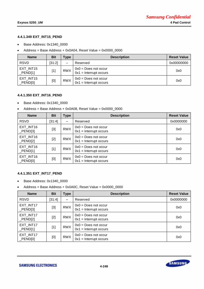
Samsung Confidential Exynos 5250_UM 4 Pad Control
4-248
4.4.1.349 EXT_INT15_PEND
Base Address: 0x1340_0000
Address = Base Address + 0x0A04, Reset Value = 0x0000_0000
Name Bit Type Description Reset Value
RSVD [31:2] – Reserved 0x00000000
EXT_INT15
_PEND[1] [1] RWX
0x0 = Does not occur
0x1 = Interrupt occurs 0x0
EXT_INT15
_PEND[0] [0] RWX
0x0 = Does not occur
0x1 = Interrupt occurs 0x0
4.4.1.350 EXT_INT16_PEND
Base Address: 0x1340_0000
Address = Base Address + 0x0A08, Reset Value = 0x0000_0000
Name Bit Type Description Reset Value
RSVD [31:4] – Reserved 0x0000000
EXT_INT16
_PEND[3] [3] RWX
0x0 = Does not occur
0x1 = Interrupt occurs 0x0
EXT_INT16
_PEND[2] [2] RWX
0x0 = Does not occur
0x1 = Interrupt occurs 0x0
EXT_INT16
_PEND[1] [1] RWX
0x0 = Does not occur
0x1 = Interrupt occurs 0x0
EXT_INT16
_PEND[0] [0] RWX
0x0 = Does not occur
0x1 = Interrupt occurs 0x0
4.4.1.351 EXT_INT17_PEND
Base Address: 0x1340_0000
Address = Base Address + 0x0A0C, Reset Value = 0x0000_0000
Name Bit Type Description Reset Value
RSVD [31:4] – Reserved 0x0000000
EXT_INT17
_PEND[3] [3] RWX
0x0 = Does not occur
0x1 = Interrupt occurs 0x0
EXT_INT17
_PEND[2] [2] RWX
0x0 = Does not occur
0x1 = Interrupt occurs 0x0
EXT_INT17
_PEND[1] [1] RWX
0x0 = Does not occur
0x1 = Interrupt occurs 0x0
EXT_INT17
_PEND[0] [0] RWX
0x0 = Does not occur
0x1 = Interrupt occurs 0x0

Samsung Confidential Exynos 5250_UM 4 Pad Control
4-249
4.4.1.352 EXT_INT18_PEND
Base Address: 0x1340_0000
Address = Base Address + 0x0A10, Reset Value = 0x0000_0000
Name Bit Type Description Reset Value
RSVD [31:8] – Reserved 0x000000
EXT_INT18
_PEND[7] [7] RWX
0x0 = Does not occur
0x1 = Interrupt occurs 0x0
EXT_INT18
_PEND[6] [6] RWX
0x0 = Does not occur
0x1 = Interrupt occurs 0x0
EXT_INT18
_PEND[5] [5] RWX
0x0 = Does not occur
0x1 = Interrupt occurs 0x0
EXT_INT18
_PEND[4] [4] RWX
0x0 = Does not occur
0x1 = Interrupt occurs 0x0
EXT_INT18
_PEND[3] [3] RWX
0x0 = Does not occur
0x1 = Interrupt occurs 0x0
EXT_INT18
_PEND[2] [2] RWX
0x0 = Does not occur
0x1 = Interrupt occurs 0x0
EXT_INT18
_PEND[1] [1] RWX
0x0 = Does not occur
0x1 = Interrupt occurs 0x0
EXT_INT18
_PEND[0] [0] RWX
0x0 = Does not occur
0x1 = Interrupt occurs 0x0

Samsung Confidential Exynos 5250_UM 4 Pad Control
4-250
4.4.1.353 EXT_INT19_PEND
Base Address: 0x1340_0000
Address = Base Address + 0x0A14, Reset Value = 0x0000_0000
Name Bit Type Description Reset Value
RSVD [31:8] – Reserved 0x000000
EXT_INT19
_PEND[7] [7] RWX
0x0 = Does not occur
0x1 = Interrupt occurs 0x0
EXT_INT19
_PEND[6] [6] RWX
0x0 = Does not occur
0x1 = Interrupt occurs 0x0
EXT_INT19
_PEND[5] [5] RWX
0x0 = Does not occur
0x1 = Interrupt occurs 0x0
EXT_INT19
_PEND[4] [4] RWX
0x0 = Does not occur
0x1 = Interrupt occurs 0x0
EXT_INT19
_PEND[3] [3] RWX
0x0 = Does not occur
0x1 = Interrupt occurs 0x0
EXT_INT19
_PEND[2] [2] RWX
0x0 = Does not occur
0x1 = Interrupt occurs 0x0
EXT_INT19
_PEND[1] [1] RWX
0x0 = Does not occur
0x1 = Interrupt occurs 0x0
EXT_INT19
_PEND[0] [0] RWX
0x0 = Does not occur
0x1 = Interrupt occurs 0x0

Samsung Confidential Exynos 5250_UM 4 Pad Control
4-251
4.4.1.354 EXT_INT20_PEND
Base Address: 0x1340_0000
Address = Base Address + 0x0A18, Reset Value = 0x0000_0000
Name Bit Type Description Reset Value
RSVD [31:2] – Reserved 0x00000000
EXT_INT20
_PEND[1] [1] RWX
0x0 = Does not occur
0x1 = Interrupt occurs 0x0
EXT_INT20
_PEND[0] [0] RWX
0x0 = Does not occur
0x1 = Interrupt occurs 0x0
4.4.1.355 EXT_INT21_PEND
Base Address: 0x1340_0000
Address = Base Address + 0x0A1C, Reset Value = 0x0000_0000
Name Bit Type Description Reset Value
RSVD [31:4] – Reserved 0x0000000
EXT_INT21
_PEND[3] [3] RWX
0x0 = Does not occur
0x1 = Interrupt occurs 0x0
EXT_INT21
_PEND[2] [2] RWX
0x0 = Does not occur
0x1 = Interrupt occurs 0x0
EXT_INT21
_PEND[1] [1] RWX
0x0 = Does not occur
0x1 = Interrupt occurs 0x0
EXT_INT21
_PEND[0] [0] RWX
0x0 = Does not occur
0x1 = Interrupt occurs 0x0

Samsung Confidential Exynos 5250_UM 4 Pad Control
4-252
4.4.1.356 EXT_INT22_PEND
Base Address: 0x1340_0000
Address = Base Address + 0x0A20, Reset Value = 0x0000_0000
Name Bit Type Description Reset Value
RSVD [31:8] – Reserved 0x000000
EXT_INT22
_PEND[7] [7] RWX
0x0 = Does not occur
0x1 = Interrupt occurs 0x0
EXT_INT22
_PEND[6] [6] RWX
0x0 = Does not occur
0x1 = Interrupt occurs 0x0
EXT_INT22
_PEND[5] [5] RWX
0x0 = Does not occur
0x1 = Interrupt occurs 0x0
EXT_INT22
_PEND[4] [4] RWX
0x0 = Does not occur
0x1 = Interrupt occurs 0x0
EXT_INT22
_PEND[3] [3] RWX
0x0 = Does not occur
0x1 = Interrupt occurs 0x0
EXT_INT22
_PEND[2] [2] RWX
0x0 = Does not occur
0x1 = Interrupt occurs 0x0
EXT_INT22
_PEND[1] [1] RWX
0x0 = Does not occur
0x1 = Interrupt occurs 0x0
EXT_INT22
_PEND[0] [0] RWX
0x0 = Does not occur
0x1 = Interrupt occurs 0x0
4.4.1.357 EXT_INT_GRPPRI_XB
Base Address: 0x1340_0000
Address = Base Address + 0x0B00, Reset Value = 0x0000_0000
Name Bit Type Description Reset Value
RSVD [31:1] – Reserved 0x00000000
EXT_INT
_GRPPRI [0] RW
EXT_INT groups priority rotate enable
0x0 = Does not rotate (Fixed)
0x1 = Enables rotate
0x0
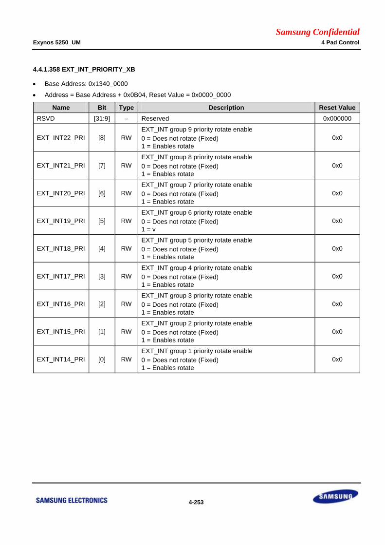
Samsung Confidential Exynos 5250_UM 4 Pad Control
4-253
4.4.1.358 EXT_INT_PRIORITY_XB
Base Address: 0x1340_0000
Address = Base Address + 0x0B04, Reset Value = 0x0000_0000
Name Bit Type Description Reset Value
RSVD [31:9] – Reserved 0x000000
EXT_INT22_PRI [8] RW
EXT_INT group 9 priority rotate enable
0 = Does not rotate (Fixed)
1 = Enables rotate
0x0
EXT_INT21_PRI [7] RW
EXT_INT group 8 priority rotate enable
0 = Does not rotate (Fixed)
1 = Enables rotate
0x0
EXT_INT20_PRI [6] RW
EXT_INT group 7 priority rotate enable
0 = Does not rotate (Fixed)
1 = Enables rotate
0x0
EXT_INT19_PRI [5] RW
EXT_INT group 6 priority rotate enable
0 = Does not rotate (Fixed)
1 = v
0x0
EXT_INT18_PRI [4] RW
EXT_INT group 5 priority rotate enable
0 = Does not rotate (Fixed)
1 = Enables rotate
0x0
EXT_INT17_PRI [3] RW
EXT_INT group 4 priority rotate enable
0 = Does not rotate (Fixed)
1 = Enables rotate
0x0
EXT_INT16_PRI [2] RW
EXT_INT group 3 priority rotate enable
0 = Does not rotate (Fixed)
1 = Enables rotate
0x0
EXT_INT15_PRI [1] RW
EXT_INT group 2 priority rotate enable
0 = Does not rotate (Fixed)
1 = Enables rotate
0x0
EXT_INT14_PRI [0] RW
EXT_INT group 1 priority rotate enable
0 = Does not rotate (Fixed)
1 = Enables rotate
0x0

Samsung Confidential Exynos 5250_UM 4 Pad Control
4-254
4.4.1.359 EXT_INT_SERVICE_XB
Base Address: 0x1340_0000
Address = Base Address + 0x0B08, Reset Value = 0x0000_0000
Name Bit Type Description Reset Value
RSVD [31:8] RW Reserved 0x0000000
SVC_Group
_Num [7:3] RW EXT_INT Service group number 0x00
SVC_Num [2:0] RW Services this Interrupt number 0x0
4.4.1.360 EXT_INT_SERVICE_PEND_XB
Base Address: 0x1340_0000
Address = Base Address + 0x0B0C, Reset Value = 0x0000_0000
Name Bit Type Description Reset Value
RSVD [31:8] RW Reserved 0x0000000
SVC_PEND [7:0] RW 0x0 = Does not occur
0x1 = Interrupt occurs 0x00
4.4.1.361 EXT_INT_GRPFIXPRI_XB
Base Address: 0x1340_0000
Address = Base Address + 0x0B10, Reset Value = 0x0000_0000
Name Bit Type Description Reset Value
RSVD [31:5] – Reserved 0x0000000
Highest_GRP
_NUM [4:0] RW
Group number of the highest priority when fixed group
priority mode: 1 to 25 0x00

Samsung Confidential Exynos 5250_UM 4 Pad Control
4-255
4.4.1.362 EXT_INT14_FIXPRI
Base Address: 0x1340_0000
Address = Base Address + 0x0B14, Reset Value = 0x0000_0000
Name Bit Type Description Reset Value
RSVD [31:3] – Reserved 0x00000000
Highest_EINT
_NUM [2:0] RW
Interrupt number of the highest priority in External Interrupt
Group 1 (EXT_INT14) when fixed priority mode: 0 to 7 0x0
4.4.1.363 EXT_INT15_FIXPRI
Base Address: 0x1340_0000
Address = Base Address + 0x0B18, Reset Value = 0x0000_0000
Name Bit Type Description Reset Value
RSVD [31:3] – Reserved 0x00000000
Highest_EINT
_NUM [2:0] RW
Interrupt number of the highest priority in External Interrupt
Group 2 (EXT_INT15) when fixed priority mode: 0 to 7 0x0
4.4.1.364 EXT_INT16_FIXPRI
Base Address: 0x1340_0000
Address = Base Address + 0x0B1C, Reset Value = 0x0000_0000
Name Bit Type Description Reset Value
RSVD [31:3] – Reserved 0x00000000
Highest_EINT
_NUM [2:0] RW
Interrupt number of the highest priority in External Interrupt
Group 3 (EXT_INT16) when fixed priority mode: 0 to 7 0x0

Samsung Confidential Exynos 5250_UM 4 Pad Control
4-256
4.4.1.365 EXT_INT17_FIXPRI
Base Address: 0x1340_0000
Address = Base Address + 0x0B20, Reset Value = 0x0000_0000
Name Bit Type Description Reset Value
RSVD [31:3] – Reserved 0x00000000
Highest_EINT
_NUM [2:0] RW
Interrupt number of the highest priority in External Interrupt
Group 4 (EXT_INT17) when fixed priority mode: 0 to 7 0x0
4.4.1.366 EXT_INT18_FIXPRI
Base Address: 0x1340_0000
Address = Base Address + 0x0B24, Reset Value = 0x0000_0000
Name Bit Type Description Reset Value
RSVD [31:3] – Reserved 0x00000000
Highest_EINT
_NUM [2:0] RW
Interrupt number of the highest priority in External Interrupt
Group 5 (EXT_INT18) when fixed priority mode: 0 to 7 0x0
4.4.1.367 EXT_INT19_FIXPRI
Base Address: 0x1340_0000
Address = Base Address + 0x0B28, Reset Value = 0x0000_0000
Name Bit Type Description Reset Value
RSVD [31:3] – Reserved 0x00000000
Highest_EINT
_NUM [2:0] RW
Interrupt number of the highest priority in External Interrupt
Group 6 (EXT_INT19) when fixed priority mode: 0 to 7 0x0
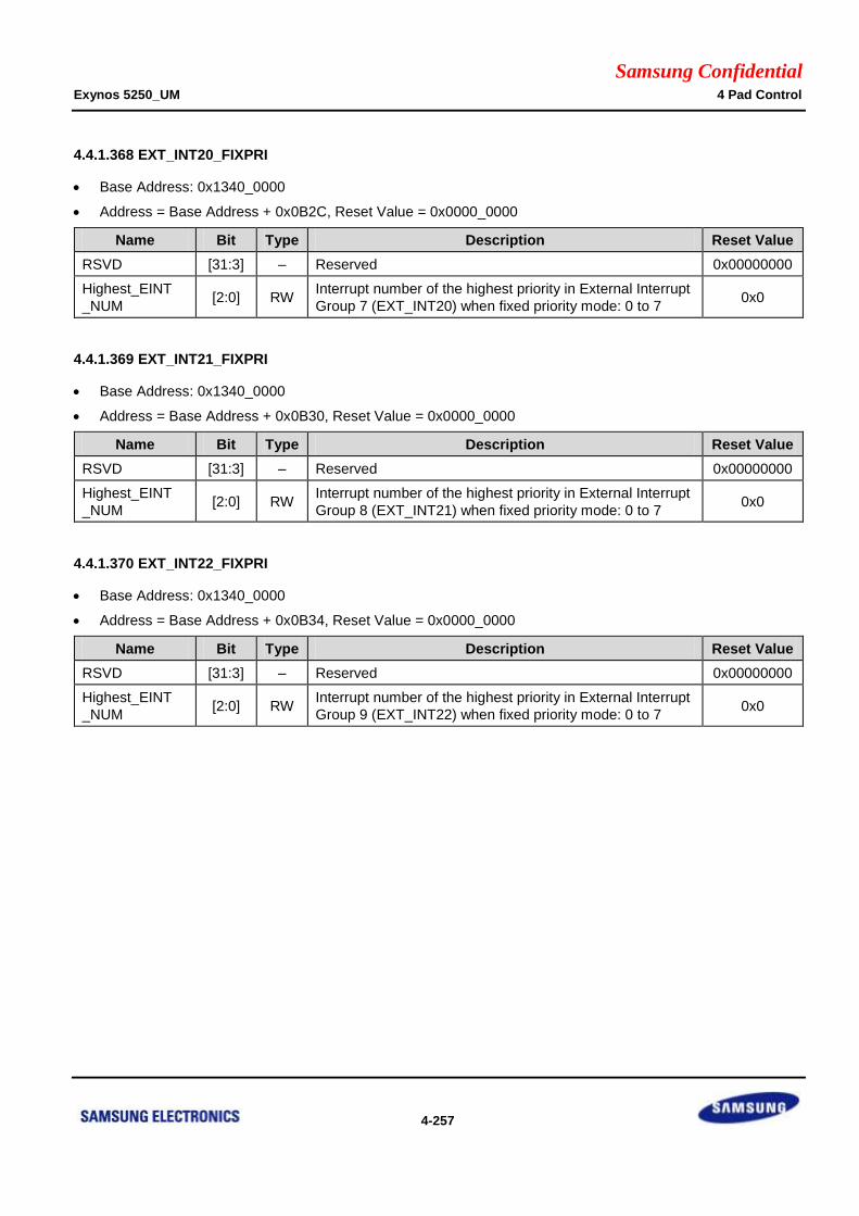
Samsung Confidential Exynos 5250_UM 4 Pad Control
4-257
4.4.1.368 EXT_INT20_FIXPRI
Base Address: 0x1340_0000
Address = Base Address + 0x0B2C, Reset Value = 0x0000_0000
Name Bit Type Description Reset Value
RSVD [31:3] – Reserved 0x00000000
Highest_EINT
_NUM [2:0] RW
Interrupt number of the highest priority in External Interrupt
Group 7 (EXT_INT20) when fixed priority mode: 0 to 7 0x0
4.4.1.369 EXT_INT21_FIXPRI
Base Address: 0x1340_0000
Address = Base Address + 0x0B30, Reset Value = 0x0000_0000
Name Bit Type Description Reset Value
RSVD [31:3] – Reserved 0x00000000
Highest_EINT
_NUM [2:0] RW
Interrupt number of the highest priority in External Interrupt
Group 8 (EXT_INT21) when fixed priority mode: 0 to 7 0x0
4.4.1.370 EXT_INT22_FIXPRI
Base Address: 0x1340_0000
Address = Base Address + 0x0B34, Reset Value = 0x0000_0000
Name Bit Type Description Reset Value
RSVD [31:3] – Reserved 0x00000000
Highest_EINT
_NUM [2:0] RW
Interrupt number of the highest priority in External Interrupt
Group 9 (EXT_INT22) when fixed priority mode: 0 to 7 0x0
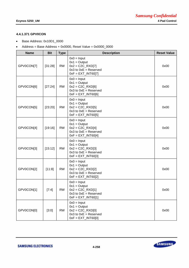
Samsung Confidential Exynos 5250_UM 4 Pad Control
4-258
4.4.1.371 GPV0CON
Base Address: 0x10D1_0000
Address = Base Address + 0x0000, Reset Value = 0x0000_0000
Name Bit Type Description Reset Value
GPV0CON[7] [31:28] RW
0x0 = Input
0x1 = Output
0x2 = C2C_RXD[7]
0x3 to 0xE = Reserved
0xF = EXT_INT60[7]
0x00
GPV0CON[6] [27:24] RW
0x0 = Input
0x1 = Output
0x2 = C2C_RXD[6]
0x3 to 0xE = Reserved
0xF = EXT_INT60[6]
0x00
GPV0CON[5] [23:20] RW
0x0 = Input
0x1 = Output
0x2 = C2C_RXD[5]
0x3 to 0xE = Reserved
0xF = EXT_INT60[5]
0x00
GPV0CON[4] [19:16] RW
0x0 = Input
0x1 = Output
0x2 = C2C_RXD[4]
0x3 to 0xE = Reserved
0xF = EXT_INT60[4]
0x00
GPV0CON[3] [15:12] RW
0x0 = Input
0x1 = Output
0x2 = C2C_RXD[3]
0x3 to 0xE = Reserved
0xF = EXT_INT60[3]
0x00
GPV0CON[2] [11:8] RW
0x0 = Input
0x1 = Output
0x2 = C2C_RXD[2]
0x3 to 0xE = Reserved
0xF = EXT_INT60[2]
0x00
GPV0CON[1] [7:4] RW
0x0 = Input
0x1 = Output
0x2 = C2C_RXD[1]
0x3 to 0xE = Reserved
0xF = EXT_INT60[1]
0x00
GPV0CON[0] [3:0] RW
0x0 = Input
0x1 = Output
0x2 = C2C_RXD[0]
0x3 to 0xE = Reserved
0xF = EXT_INT60[0]
0x00

Samsung Confidential Exynos 5250_UM 4 Pad Control
4-259
4.4.1.372 GPV0DAT
Base Address: 0x10D1_0000
Address = Base Address + 0x0004, Reset Value = 0x00
Name Bit Type Description Reset Value
GPV0DAT[7:0] [7:0] RWX
When you configure the port as input port, the
corresponding bit is the pin state. When you configure
the port as output port, the pin state is the same as the
corresponding bit. When you configure the port as
functional pin, the undefined value will be read.
0x00
4.4.1.373 GPV0PUD
Base Address: 0x10D1_0000
Address = Base Address + 0x0008, Reset Value = 0x5555
Name Bit Type Description Reset Value
GPV0PUD[n] [2n + 1:2n]
n = 0 to 7 RW
0x0 = Disables Pull-up/down
0x1 = Enables Pull-down
0x2 = Reserved
0x3 = Enables Pull-up
0x5555
4.4.1.374 GPV0DRV
Base Address: 0x10D1_0000
Address = Base Address + 0x000C, Reset Value = 0x00_0000
Name Bit Type Description Reset Value
GPV0DRV[n]
[2n + 1:2n]
n = 0 to 7 RW
0x0 = 1x
0x2 = 2x
0x1 = 3x
0x3 = 4x
0x00_0000
[n + 16:16]
n = 0 to 7 RW Reserved. Should be zero. 0x00_0000

Samsung Confidential Exynos 5250_UM 4 Pad Control
4-260
4.4.1.375 GPV0CONPDN
Base Address: 0x10D1_0000
Address = Base Address + 0x0010, Reset Value = 0x0000
Name Bit Type Description Reset Value
GPV0[n] [2n + 1:2n]
n = 0 to 7 RW
0x0 = Output 0
0x1 = Output 1
0x2 = Input
0x3 = Previous state
0x00
4.4.1.376 GPV0PUDPDN
Base Address: 0x10D1_0000
Address = Base Address + 0x0014, Reset Value = 0x0000
Name Bit Type Description Reset Value
GPV0[n] [2n + 1:2n]
n = 0 to 7 RW
0x0 = Disables Pull-up/down
0x1 = Enables Pull-down
0x2 = Reserved
0x3 = Enables Pull-up enabled
0x00

Samsung Confidential Exynos 5250_UM 4 Pad Control
4-261
4.4.1.377 GPV1CON
Base Address: 0x10D1_0000
Address = Base Address + 0x0020, Reset Value = 0x0000_0000
Name Bit Type Description Reset Value
GPV1CON[7] [31:28] RW
0x0 = Input
0x1 = Output
0x2 = C2C_RXD[15]
0x3 to 0xE = Reserved
0xF = EXT_INT61[7]
0x00
GPV1CON[6] [27:24] RW
0x0 = Input
0x1 = Output
0x2 = C2C_RXD[14]
0x3 to 0xE = Reserved
0xF = EXT_INT61[6]
0x00
GPV1CON[5] [23:20] RW
0x0 = Input
0x1 = Output
0x2 = C2C_RXD[13]
0x3 to 0xE = Reserved
0xF = EXT_INT61[5]
0x00
GPV1CON[4] [19:16] RW
0x0 = Input
0x1 = Output
0x2 = C2C_RXD[12]
0x3 to 0xE = Reserved
0xF = EXT_INT61[4]
0x00
GPV1CON[3] [15:12] RW
0x0 = Input
0x1 = Output
0x2 = C2C_RXD[11]
0x3 to 0xE = Reserved
0xF = EXT_INT61[3]
0x00
GPV1CON[2] [11:8] RW
0x0 = Input
0x1 = Output
0x2 = C2C_RXD[10]
0x3 to 0xE = Reserved
0xF = EXT_INT61[2]
0x00
GPV1CON[1] [7:4] RW
0x0 = Input
0x1 = Output
0x2 = C2C_RXD[9]
0x3 to 0xE = Reserved
0xF = EXT_INT61[1]
0x00
GPV1CON[0] [3:0] RW
0x0 = Input
0x1 = Output
0x2 = C2C_RXD[8]
0x3 to 0xE = Reserved
0xF = EXT_INT61[0]
0x00

Samsung Confidential Exynos 5250_UM 4 Pad Control
4-262
4.4.1.378 GPV1DAT
Base Address: 0x10D1_0000
Address = Base Address + 0x0024, Reset Value = 0x00
Name Bit Type Description Reset Value
GPV1DAT[7:0] [7:0] RWX
When you configure the port as input port, the
corresponding bit is the pin state. When you configure
the port as output port, the pin state is the same as the
corresponding bit. When you configure the port as
functional pin, the undefined value will be read.
0x00
4.4.1.379 GPV1PUD
Base Address: 0x10D1_0000
Address = Base Address + 0x0028, Reset Value = 0x5555
Name Bit Type Description Reset Value
GPV1PUD[n] [2n + 1:2n]
n = 0 to 7 RW
0x0 = Disables Pull-up/down
0x1 = Enables Pull-down
0x2 = Reserved
0x3 = Enables Pull-up
0x5555
4.4.1.380 GPV1DRV
Base Address: 0x10D1_0000
Address = Base Address + 0x002C, Reset Value = 0x00_0000
Name Bit Type Description Reset Value
GPV1DRV[n]
[2n + 1:2n]
n = 0 to 7 RW
0x0 = 1x
0x2 = 2x
0x1 = 3x
0x3 = 4x
0x00_0000
[n + 16:16]
n = 0 to 7 RW Reserved. Should be zero. 0x00_0000

Samsung Confidential Exynos 5250_UM 4 Pad Control
4-263
4.4.1.381 GPV1CONPDN
Base Address: 0x10D1_0000
Address = Base Address + 0x0030, Reset Value = 0x0000
Name Bit Type Description Reset Value
GPV1[n] [2n + 1:2n]
n = 0 to 7 RW
0x0 = Output 0
0x1 = Output 1
0x2 = Input
0x3 = Previous state
0x00
4.4.1.382 GPV1PUDPDN
Base Address: 0x10D1_0000
Address = Base Address + 0x0034, Reset Value = 0x0000
Name Bit Type Description Reset Value
GPV1[n] [2n + 1:2n]
n = 0 to 7 RW
0x0 = Disables Pull-up/down
0x1 = Enables Pull-down
0x2 = Reserved
0x3 = Enables Pull-up
0x00
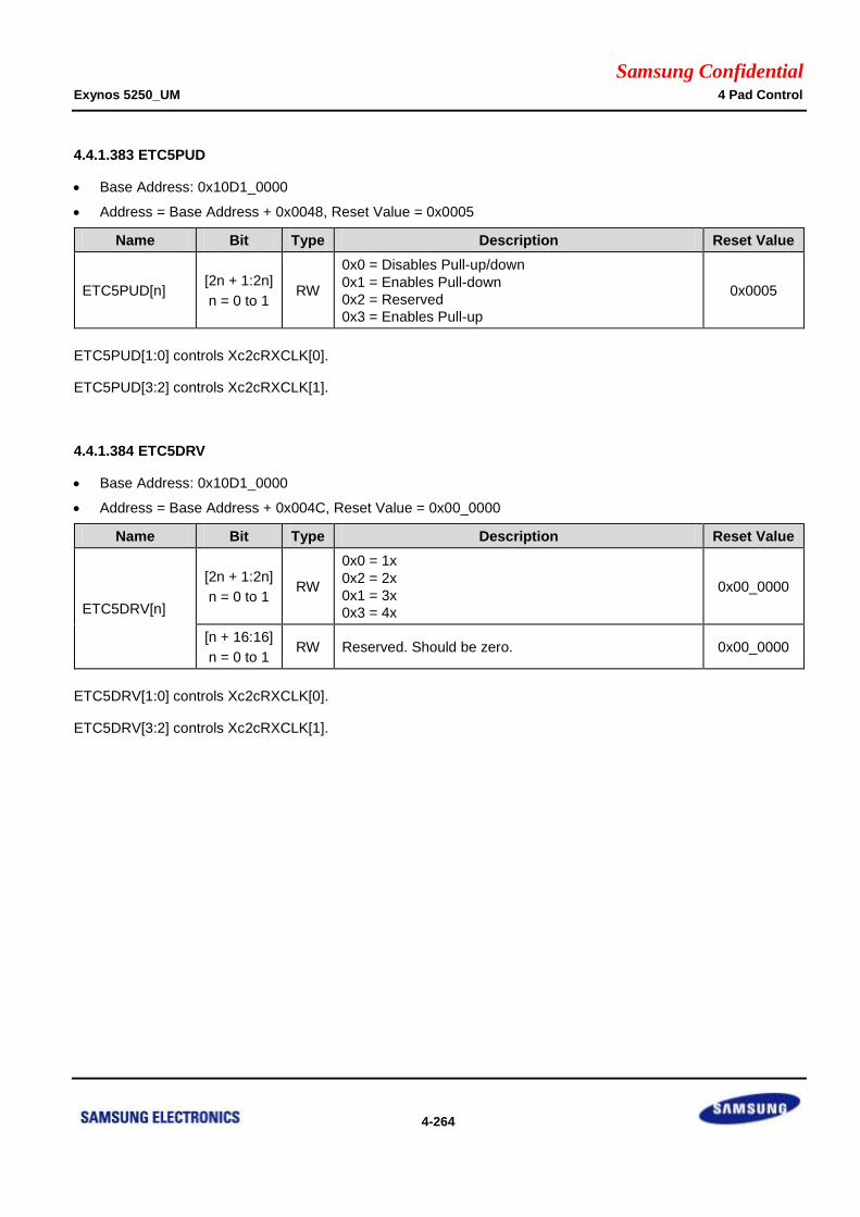
Samsung Confidential Exynos 5250_UM 4 Pad Control
4-264
4.4.1.383 ETC5PUD
Base Address: 0x10D1_0000
Address = Base Address + 0x0048, Reset Value = 0x0005
Name Bit Type Description Reset Value
ETC5PUD[n] [2n + 1:2n]
n = 0 to 1 RW
0x0 = Disables Pull-up/down
0x1 = Enables Pull-down
0x2 = Reserved
0x3 = Enables Pull-up
0x0005
ETC5PUD[1:0] controls Xc2cRXCLK[0].
ETC5PUD[3:2] controls Xc2cRXCLK[1].
4.4.1.384 ETC5DRV
Base Address: 0x10D1_0000
Address = Base Address + 0x004C, Reset Value = 0x00_0000
Name Bit Type Description Reset Value
ETC5DRV[n]
[2n + 1:2n]
n = 0 to 1 RW
0x0 = 1x
0x2 = 2x
0x1 = 3x
0x3 = 4x
0x00_0000
[n + 16:16]
n = 0 to 1 RW Reserved. Should be zero. 0x00_0000
ETC5DRV[1:0] controls Xc2cRXCLK[0].
ETC5DRV[3:2] controls Xc2cRXCLK[1].

Samsung Confidential Exynos 5250_UM 4 Pad Control
4-265
4.4.1.385 GPV2CON
Base Address: 0x10D1_0000
Address = Base Address + 0x0060, Reset Value = 0x0000_0000
Name Bit Type Description Reset Value
GPV2CON[7] [31:28] RW
0x0 = Input
0x1 = Output
0x2 = C2C_TXD[7]
0x3 to 0xE = Reserved
0xF = EXT_INT62[7]
0x00
GPV2CON[6] [27:24] RW
0x0 = Input
0x1 = Output
0x2 = C2C_TXD[6]
0x3 to 0xE = Reserved
0xF = EXT_INT62[6]
0x00
GPV2CON[5] [23:20] RW
0x0 = Input
0x1 = Output
0x2 = C2C_TXD[5]
0x3 to 0xE = Reserved
0xF = EXT_INT62[5]
0x00
GPV2CON[4] [19:16] RW
0x0 = Input
0x1 = Output
0x2 = C2C_TXD[4]
0x3 to 0xE = Reserved
0xF = EXT_INT62[4]
0x00
GPV2CON[3] [15:12] RW
0x0 = Input
0x1 = Output
0x2 = C2C_TXD[3]
0x3 to 0xE = Reserved
0xF = EXT_INT62[3]
0x00
GPV2CON[2] [11:8] RW
0x0 = Input
0x1 = Output
0x2 = C2C_TXD[2]
0x3 to 0xE = Reserved
0xF = EXT_INT62[2]
0x00
GPV2CON[1] [7:4] RW
0x0 = Input
0x1 = Output
0x2 = C2C_TXD[1]
0x3 to 0xE = Reserved
0xF = EXT_INT62[1]
0x00
GPV2CON[0] [3:0] RW
0x0 = Input
0x1 = Output
0x2 = C2C_TXD[0]
0x3 to 0xE = Reserved
0xF = EXT_INT62[0]
0x00

Samsung Confidential Exynos 5250_UM 4 Pad Control
4-266
4.4.1.386 GPV2DAT
Base Address: 0x10D1_0000
Address = Base Address + 0x0064, Reset Value = 0x00
Name Bit Type Description Reset Value
GPV2DAT[7:0] [7:0] RWX
When you configure the port as input port, the
corresponding bit is the pin state. When you configure
the port as output port, the pin state is the same as the
corresponding bit. When you configure the port as
functional pin, the undefined value will be read.
0x00
4.4.1.387 GPV2PUD
Base Address: 0x10D1_0000
Address = Base Address + 0x0068, Reset Value = 0x5555
Name Bit Type Description Reset Value
GPV2PUD[n] [2n + 1:2n]
n = 0 to 7 RW
0x0 = Disables Pull-up/down
0x1 = Enables Pull-down
0x2 = Reserved
0x3 = Enables Pull-up
0x5555
4.4.1.388 GPV2DRV
Base Address: 0x10D1_0000
Address = Base Address + 0x006C, Reset Value = 0x00_0000
Name Bit Type Description Reset Value
GPV2DRV[n]
[2n + 1:2n]
n = 0 to 7 RW
0x0 = 1x
0x2 = 2x
0x1 = 3x
0x3 = 4x
0x00_0000
[n + 16:16]
n = 0 to 7 RW Reserved. Should be zero. 0x00_0000

Samsung Confidential Exynos 5250_UM 4 Pad Control
4-267
4.4.1.389 GPV2CONPDN
Base Address: 0x10D1_0000
Address = Base Address + 0x0070, Reset Value = 0x0000
Name Bit Type Description Reset Value
GPV2[n] [2n + 1:2n]
n = 0 to 7 RW
0x0 = Output 0
0x1 = Output 1
0x2 = Input
0x3 = Previous state
0x00
4.4.1.390 GPV2PUDPDN
Base Address: 0x10D1_0000
Address = Base Address + 0x0074, Reset Value = 0x0000
Name Bit Type Description Reset Value
GPV2[n] [2n + 1:2n]
n = 0 to 7 RW
0x0 = Disables Pull-up/down
0x1 = Enables Pull-down
0x2 = Reserved
0x3 = Enables Pull-up
0x00

Samsung Confidential Exynos 5250_UM 4 Pad Control
4-268
4.4.1.391 GPV3CON
Base Address: 0x10D1_0000
Address = Base Address + 0x0080, Reset Value = 0x0000_0000
Name Bit Type Description Reset Value
GPV3CON[7] [31:28] RW
0x0 = Input
0x1 = Output
0x2 = C2C_TXD[15]
0x3 to 0xE = Reserved
0xF = EXT_INT63[7]
0x00
GPV3CON[6] [27:24] RW
0x0 = Input
0x1 = Output
0x2 = C2C_TXD[14]
0x3 to 0xE = Reserved
0xF = EXT_INT63[6]
0x00
GPV3CON[5] [23:20] RW
0x0 = Input
0x1 = Output
0x2 = C2C_TXD[13]
0x3 to 0xE = Reserved
0xF = EXT_INT63[5]
0x00
GPV3CON[4] [19:16] RW
0x0 = Input
0x1 = Output
0x2 = C2C_TXD[12]
0x3 to 0xE = Reserved
0xF = EXT_INT63[4]
0x00
GPV3CON[3] [15:12] RW
0x0 = Input
0x1 = Output
0x2 = C2C_TXD[11]
0x3 to 0xE = Reserved
0xF = EXT_INT63[3]
0x00
GPV3CON[2] [11:8] RW
0x0 = Input
0x1 = Output
0x2 = C2C_TXD[10]
0x3 to 0xE = Reserved
0xF = EXT_INT63[2]
0x00
GPV3CON[1] [7:4] RW
0x0 = Input
0x1 = Output
0x2 = C2C_TXD[9]
0x3 to 0xE = Reserved
0xF = EXT_INT63[1]
0x00
GPV3CON[0] [3:0] RW
0x0 = Input
0x1 = Output
0x2 = C2C_TXD[8]
0x3 to 0xE = Reserved
0xF = EXT_INT63[0]
0x00

Samsung Confidential Exynos 5250_UM 4 Pad Control
4-269
4.4.1.392 GPV3DAT
Base Address: 0x10D1_0000
Address = Base Address + 0x0084, Reset Value = 0x00
Name Bit Type Description Reset Value
GPV3DAT[7:0] [7:0] RWX
When you configure the port as input port, the
corresponding bit is the pin state. When you configure
the port as output port, the pin state is the same as the
corresponding bit. When you configure the port as
functional pin, the undefined value will be read.
0x00
4.4.1.393 GPV3PUD
Base Address: 0x10D1_0000
Address = Base Address + 0x0088, Reset Value = 0x5555
Name Bit Type Description Reset Value
GPV3PUD[n] [2n + 1:2n]
n = 0 to 7 RW
0x0 = Disables Pull-up/down
0x1 = Enables Pull-down
0x2 = Reserved
0x3 = Enables Pull-up
0x5555
4.4.1.394 GPV3DRV
Base Address: 0x10D1_0000
Address = Base Address + 0x008C, Reset Value = 0x00_0000
Name Bit Type Description Reset Value
GPV3DRV[n]
[2n + 1:2n]
n = 0 to 7 RW
0x0 = 1x
0x2 = 2x
0x1 = 3x
0x3 = 4x
0x00_0000
[n + 16:16]
n = 0 to 7 RW Reserved. Should be zero. 0x00_0000

Samsung Confidential Exynos 5250_UM 4 Pad Control
4-270
4.4.1.395 GPV3CONPDN
Base Address: 0x10D1_0000
Address = Base Address + 0x0090, Reset Value = 0x0000
Name Bit Type Description Reset Value
GPV3[n] [2n + 1:2n]
n = 0 to 7 RW
0x0 = Output 0
0x1 = Output 1
0x2 = Input
0x3 = Previous state
0x00
4.4.1.396 GPV3PUDPDN
Base Address: 0x10D1_0000
Address = Base Address + 0x0094, Reset Value = 0x0000
Name Bit Type Description Reset Value
GPV3[n] [2n + 1:2n]
n = 0 to 7 RW
0x0 = Disables Pull-up/down
0x1 = Enables Pull-down
0x2 = Reserved
0x3 = Enables Pull-up
0x00

Samsung Confidential Exynos 5250_UM 4 Pad Control
4-271
4.4.1.397 ETC8PUD
Base Address: 0x10D1_0000
Address = Base Address + 0x00A8, Reset Value = 0x0000
Name Bit Type Description Reset Value
ETC8PUD[n] [2n + 1:2n]
n = 0 to 1 RW
0x0 = Disables Pull-up/down
0x1 = Enables Pull-down
0x2 = Reserved
0x3 = Enables Pull-up
0x0000
ETC8PUD[1:0] controls Xc2cTXCLK[0].
ETC8PUD[3:2] controls Xc2cTXCLK[1].
4.4.1.398 ETC8DRV
Base Address: 0x10D1_0000
Address = Base Address + 0x00AC, Reset Value = 0x00_0000
Name Bit Type Description Reset Value
ETC8DRV[n]
[2n + 1:2n]
n = 0 to 1 RW
0x0 = 1x
0x2 = 2x
0x1 = 3x
0x3 = 4x
0x00_0000
[n + 16:16]
n = 0 to 1 RW Reserved. Should be zero. 0x00_0000
ETC8DRV[1:0] controls Xc2cTXCLK[0].
ETC8DRV[3:2] controls Xc2cTXCLK[1].
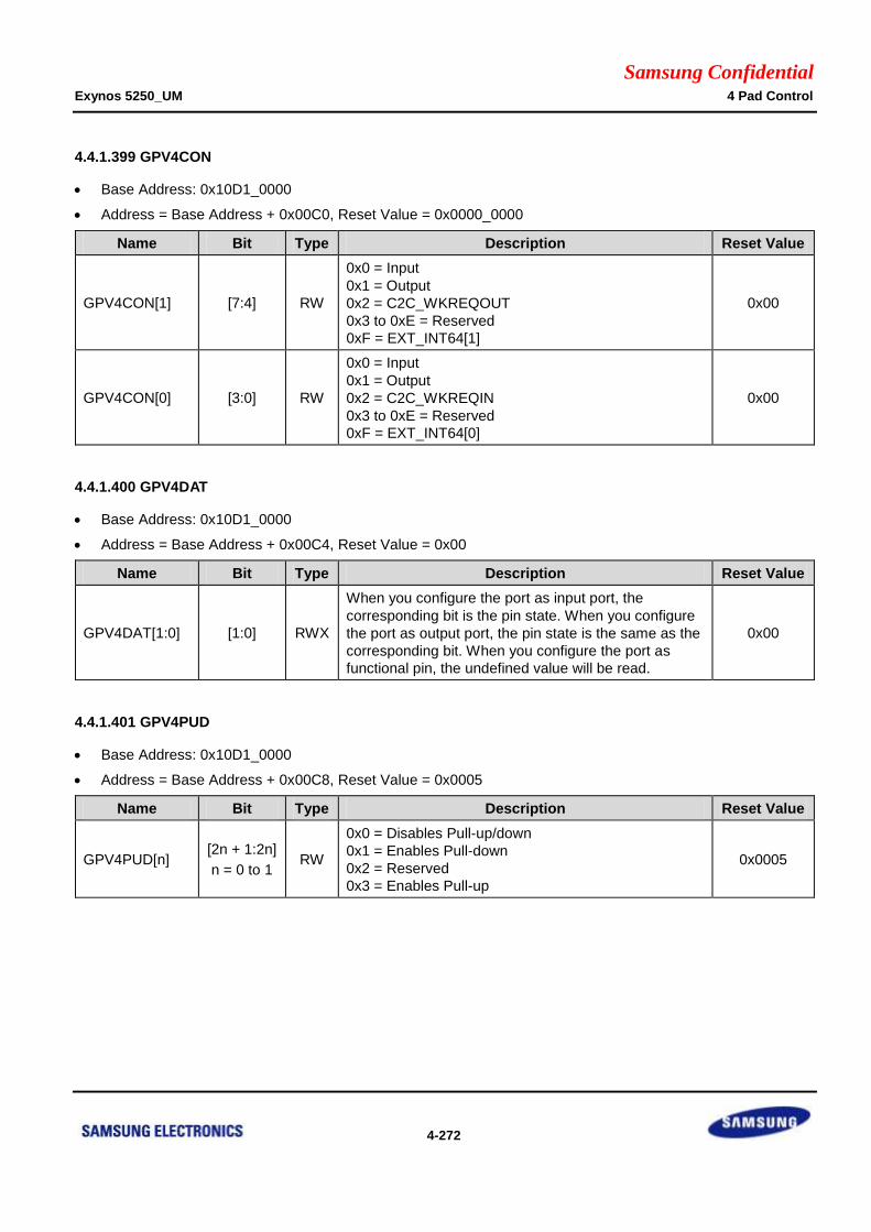
Samsung Confidential Exynos 5250_UM 4 Pad Control
4-272
4.4.1.399 GPV4CON
Base Address: 0x10D1_0000
Address = Base Address + 0x00C0, Reset Value = 0x0000_0000
Name Bit Type Description Reset Value
GPV4CON[1] [7:4] RW
0x0 = Input
0x1 = Output
0x2 = C2C_WKREQOUT
0x3 to 0xE = Reserved
0xF = EXT_INT64[1]
0x00
GPV4CON[0] [3:0] RW
0x0 = Input
0x1 = Output
0x2 = C2C_WKREQIN
0x3 to 0xE = Reserved
0xF = EXT_INT64[0]
0x00
4.4.1.400 GPV4DAT
Base Address: 0x10D1_0000
Address = Base Address + 0x00C4, Reset Value = 0x00
Name Bit Type Description Reset Value
GPV4DAT[1:0] [1:0] RWX
When you configure the port as input port, the
corresponding bit is the pin state. When you configure
the port as output port, the pin state is the same as the
corresponding bit. When you configure the port as
functional pin, the undefined value will be read.
0x00
4.4.1.401 GPV4PUD
Base Address: 0x10D1_0000
Address = Base Address + 0x00C8, Reset Value = 0x0005
Name Bit Type Description Reset Value
GPV4PUD[n] [2n + 1:2n]
n = 0 to 1 RW
0x0 = Disables Pull-up/down
0x1 = Enables Pull-down
0x2 = Reserved
0x3 = Enables Pull-up
0x0005
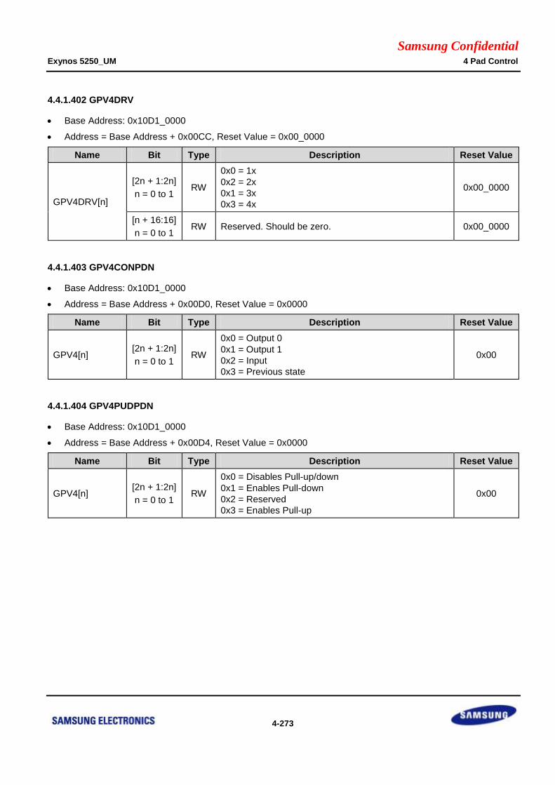
Samsung Confidential Exynos 5250_UM 4 Pad Control
4-273
4.4.1.402 GPV4DRV
Base Address: 0x10D1_0000
Address = Base Address + 0x00CC, Reset Value = 0x00_0000
Name Bit Type Description Reset Value
GPV4DRV[n]
[2n + 1:2n]
n = 0 to 1 RW
0x0 = 1x
0x2 = 2x
0x1 = 3x
0x3 = 4x
0x00_0000
[n + 16:16]
n = 0 to 1 RW Reserved. Should be zero. 0x00_0000
4.4.1.403 GPV4CONPDN
Base Address: 0x10D1_0000
Address = Base Address + 0x00D0, Reset Value = 0x0000
Name Bit Type Description Reset Value
GPV4[n] [2n + 1:2n]
n = 0 to 1 RW
0x0 = Output 0
0x1 = Output 1
0x2 = Input
0x3 = Previous state
0x00
4.4.1.404 GPV4PUDPDN
Base Address: 0x10D1_0000
Address = Base Address + 0x00D4, Reset Value = 0x0000
Name Bit Type Description Reset Value
GPV4[n] [2n + 1:2n]
n = 0 to 1 RW
0x0 = Disables Pull-up/down
0x1 = Enables Pull-down
0x2 = Reserved
0x3 = Enables Pull-up
0x00

Samsung Confidential Exynos 5250_UM 4 Pad Control
4-274
4.4.1.405 EXT_INT60CON
Base Address: 0x10D1_0000
Address = Base Address + 0x0700, Reset Value = 0x0000_0000
Name Bit Type Description Reset Value
RSVD [31] – Reserved 0x0
EXT_INT60
_CON[7] [30:28] RW
Setting the signaling method of EXT_INT60[7]
0x0 = Sets Low level
0x1 = Sets High level
0x2 = Triggers Falling edge
0x3 = Triggers Rising edge
0x4 = Triggers Both edge
0x5 to 0x7 = Reserved
0x0
RSVD [27] – Reserved 0x0
EXT_INT60
_CON[6] [26:24] RW
Setting the signaling method of EXT_INT60[6]
0x0 = Sets Low level
0x1 = Sets High level
0x2 = Triggers Falling edge
0x3 = Triggers Rising edge
0x4 = Triggers Both edge
0x5 to 0x7 = Reserved
0x0
RSVD [23] – Reserved 0x0
EXT_INT60
_CON[5] [22:20] RW
Setting the signaling method of EXT_INT60[5]
0x0 = Sets Low level
0x1 = Sets High level
0x2 = Triggers Falling edge
0x3 = Triggers Rising edge
0x4 = Triggers Both edge
0x5 to 0x7 = Reserved
0x0
RSVD [19] – Reserved 0x0
EXT_INT60
_CON[4] [18:16] RW
Setting the signaling method of EXT_INT60[4]
0x0 = Sets Low level
0x1 = Sets High level
0x2 = Triggers Falling edge
0x3 = Triggers Rising edge
0x4 = Triggers Both edge
0x5 to 0x7 = Reserved
0x0
RSVD [15] – Reserved 0x0
EXT_INT60
_CON[3] [14:12] RW
Setting the signaling method of EXT_INT60[3]
0x0 = Sets Low level
0x1 = Sets High level
0x2 = Triggers Falling edge
0x3 = Triggers Rising edge
0x4 = Triggers Both edge
0x5 to 0x7 = Reserved
0x0
RSVD [11] – Reserved 0x0
EXT_INT60 [10:8] RW Setting the signaling method of EXT_INT60[2] 0x0

Samsung Confidential Exynos 5250_UM 4 Pad Control
4-275
Name Bit Type Description Reset Value
_CON[2] 0x0 = Sets Low level
0x1 = Sets High level
0x2 = Triggers Falling edge triggered
0x3 = Triggers Rising edge
0x4 = Triggers Both edge
0x5 to 0x7 = Reserved
RSVD [7] – Reserved 0x0
EXT_INT60
_CON[1] [6:4] RW
Setting the signaling method of EXT_INT60[1]
0x0 = Sets Low level
0x1 = Sets High level
0x2 = Triggers Falling edge
0x3 = Triggers Rising edge
0x4 = Triggers Both edge
0x5 to 0x7 = Reserved
0x0
RSVD [3] – Reserved 0x0
EXT_INT60
_CON[0] [2:0] RW
Setting the signaling method of EXT_INT60[0]
0x0 = Sets Low level
0x1 = Sets High level
0x2 = Triggers Falling edge
0x3 = Triggers Rising edge
0x4 = Triggers Both edge
0x5 to 0x7 = Reserved
0x0

Samsung Confidential Exynos 5250_UM 4 Pad Control
4-276
4.4.1.406 EXT_INT61CON
Base Address: 0x10D1_0000
Address = Base Address + 0x0704, Reset Value = 0x0000_0000
Name Bit Type Description Reset Value
RSVD [31] – Reserved 0x0
EXT_INT61
_CON[7] [30:28] RW
Setting the signaling method of EXT_INT61[7]
0x0 = Sets Low level
0x1 = Sets High level
0x2 = Triggers Falling edge
0x3 = Triggers Rising edge
0x4 = Triggers Both edge
0x5 to 0x7 = Reserved
0x0
RSVD [27] – Reserved 0x0
EXT_INT61
_CON[6] [26:24] RW
Setting the signaling method of EXT_INT61[6]
0x0 = Sets Low level
0x1 = Sets High level
0x2 = Triggers Falling edge
0x3 = Triggers Rising edge
0x4 = Triggers Both edge
0x5 to 0x7 = Reserved
0x0
RSVD [23] – Reserved 0x0
EXT_INT61
_CON[5] [22:20] RW
Setting the signaling method of EXT_INT61[5]
0x0 = Sets Low level
0x1 = Sets High level
0x2 = Triggers Falling edge
0x3 = Triggers Rising edge
0x4 = Triggers Both edge
0x5 to 0x7 = Reserved
0x0
RSVD [19] – Reserved 0x0
EXT_INT61
_CON[4] [18:16] RW
Setting the signaling method of EXT_INT61[4]
0x0 = Sets Low level
0x1 = Sets High level
0x2 = Triggers Falling edge
0x3 = Triggers Rising edge
0x4 = Triggers Both edge
0x5 to 0x7 = Reserved
0x0
RSVD [15] – Reserved 0x0
EXT_INT61
_CON[3] [14:12] RW
Setting the signaling method of EXT_INT61[3]
0x0 = Sets Low level
0x1 = Sets High level
0x2 = Triggers Falling edge
0x3 = Triggers Rising edge
0x4 = Triggers Both edge
0x5 to 0x7 = Reserved
0x0
RSVD [11] – Reserved 0x0
EXT_INT61 [10:8] RW Setting the signaling method of EXT_INT61[2] 0x0

Samsung Confidential Exynos 5250_UM 4 Pad Control
4-277
Name Bit Type Description Reset Value
_CON[2] 0x0 = Sets Low level
0x1 = Sets High level
0x2 = Triggers Falling edge
0x3 = Triggers Rising edge
0x4 = Triggers Both edge
0x5 to 0x7 = Reserved
RSVD [7] – Reserved 0x0
EXT_INT61
_CON[1] [6:4] RW
Setting the signaling method of EXT_INT61[1]
0x0 = Sets Low level
0x1 = Sets High level
0x2 = Triggers Falling edge
0x3 = Triggers Rising edge
0x4 = Triggers Both edge
0x5 to 0x7 = Reserved
0x0
RSVD [3] – Reserved 0x0
EXT_INT61
_CON[0] [2:0] RW
Setting the signaling method of EXT_INT61[0]
0x0 = Sets Low level
0x1 = Sets High level
0x2 = Triggers Falling edge
0x3 = Triggers Rising edge
0x4 = Triggers Both edge
0x5 to 0x7 = Reserved
0x0

Samsung Confidential Exynos 5250_UM 4 Pad Control
4-278
4.4.1.407 EXT_INT62CON
Base Address: 0x10D1_0000
Address = Base Address + 0x0708, Reset Value = 0x0000_0000
Name Bit Type Description Reset Value
RSVD [31] – Reserved 0x0
EXT_INT62
_CON[7] [30:28] RW
Setting the signaling method of EXT_INT62[7]
0x0 = Sets Low level
0x1 = Sets High level
0x2 = Triggers Falling edge
0x3 = Triggers Rising edge
0x4 = Triggers Both edge
0x5 to 0x7 = Reserved
0x0
RSVD [27] – Reserved 0x0
EXT_INT62
_CON[6] [26:24] RW
Setting the signaling method of EXT_INT62[6]
0x0 = Sets Low level
0x1 = Sets High level
0x2 = Triggers Falling edge
0x3 = Triggers Rising edge
0x4 = Triggers Both edge
0x5 to 0x7 = Reserved
0x0
RSVD [23] – Reserved 0x0
EXT_INT62
_CON[5] [22:20] RW
Setting the signaling method of EXT_INT62[5]
0x0 = Sets Low level
0x1 = Sets High level
0x2 = Triggers Falling edge
0x3 = Triggers Rising edge
0x4 = Triggers Both edge
0x5 to 0x7 = Reserved
0x0
RSVD [19] – Reserved 0x0
EXT_INT62
_CON[4] [18:16] RW
Setting the signaling method of EXT_INT62[4]
0x0 = Sets Low level
0x1 = Sets High level
0x2 = Triggers Falling edge
0x3 = Triggers Rising edge
0x4 = Triggers Both edge
0x5 to 0x7 = Reserved
0x0
RSVD [15] – Reserved 0x0
EXT_INT62
_CON[3] [14:12] RW
Setting the signaling method of EXT_INT62[3]
0x0 = Sets Low level
0x1 = Sets High level
0x2 = Triggers Falling edge
0x3 = Triggers Rising edge
0x4 = Triggers Both edge
0x5 to 0x7 = Reserved
0x0
RSVD [11] – Reserved 0x0
EXT_INT62 [10:8] RW Setting the signaling method of EXT_INT62[2] 0x0

Samsung Confidential Exynos 5250_UM 4 Pad Control
4-279
Name Bit Type Description Reset Value
_CON[2] 0x0 = Sets Low level
0x1 = Sets High level
0x2 = Triggers Falling edge
0x3 = Triggers Rising edge
0x4 = Triggers Both edge
0x5 to 0x7 = Reserved
RSVD [7] – Reserved 0x0
EXT_INT62
_CON[1] [6:4] RW
Setting the signaling method of EXT_INT62[1]
0x0 = Sets Low level
0x1 = Sets High level
0x2 = Triggers Falling edge
0x3 = Triggers Rising edge
0x4 = Triggers Both edge
0x5 to 0x7 = Reserved
0x0
RSVD [3] – Reserved 0x0
EXT_INT62
_CON[0] [2:0] RW
Setting the signaling method of EXT_INT62[0]
0x0 = Sets Low level
0x1 = Sets High level
0x2 = Triggers Falling edge
0x3 = Triggers Rising edge
0x4 = Triggers Both edge
0x5 to 0x7 = Reserved
0x0

Samsung Confidential Exynos 5250_UM 4 Pad Control
4-280
4.4.1.408 EXT_INT63CON
Base Address: 0x10D1_0000
Address = Base Address + 0x070C, Reset Value = 0x0000_0000
Name Bit Type Description Reset Value
RSVD [31] – Reserved 0x0
EXT_INT63
_CON[7] [30:28] RW
Setting the signaling method of EXT_INT63[7]
0x0 = Sets Low level
0x1 = Sets High level
0x2 = Triggers Falling edge
0x3 = Triggers Rising edge
0x4 = Triggers Both edge
0x5 to 0x7 = Reserved
0x0
RSVD [27] – Reserved 0x0
EXT_INT63
_CON[6] [26:24] RW
Setting the signaling method of EXT_INT63[6]
0x0 = Sets Low level
0x1 = Sets High level
0x2 = Triggers Falling edge
0x3 = Triggers Rising edge
0x4 = Triggers Both edge
0x5 to 0x7 = Reserved
0x0
RSVD [23] – Reserved 0x0
EXT_INT63
_CON[5] [22:20] RW
Setting the signaling method of EXT_INT63[5]
0x0 = Sets Low level
0x1 = Sets High level
0x2 = Triggers Falling edge
0x3 = Triggers Rising edge
0x4 = Triggers Both edge
0x5 to 0x7 = Reserved
0x0
RSVD [19] – Reserved 0x0
EXT_INT63
_CON[4] [18:16] RW
Setting the signaling method of EXT_INT63[4]
0x0 = Sets Low level
0x1 = Sets High level
0x2 = Triggers Falling edge
0x3 = Triggers Rising edge
0x4 = Triggers Both edge
0x5 to 0x7 = Reserved
0x0
RSVD [15] – Reserved 0x0
EXT_INT63
_CON[3] [14:12] RW
Setting the signaling method of EXT_INT63[3]
0x0 = Sets Low level
0x1 = Sets High level
0x2 = Triggers Falling edge
0x3 = Triggers Rising edge
0x4 = Triggers Both edge
0x5 to 0x7 = Reserved
0x0
RSVD [11] – Reserved 0x0
EXT_INT63 [10:8] RW Setting the signaling method of EXT_INT63[2] 0x0

Samsung Confidential Exynos 5250_UM 4 Pad Control
4-281
Name Bit Type Description Reset Value
_CON[2] 0x0 = Sets Low level
0x1 = Sets High level
0x2 = Triggers Falling edge
0x3 = Triggers Rising edge
0x4 = Triggers Both edge
0x5 to 0x7 = Reserved
RSVD [7] – Reserved 0x0
EXT_INT63
_CON[1] [6:4] RW
Setting the signaling method of EXT_INT63[1]
0x0 = Sets Low level
0x1 = Sets High level
0x2 = Triggers Falling edge
0x3 = Triggers Rising edge
0x4 = Triggers Both edge
0x5 to 0x7 = Reserved
0x0
RSVD [3] – Reserved 0x0
EXT_INT63
_CON[0] [2:0] RW
Setting the signaling method of EXT_INT63[0]
0x0 = Sets Low level
0x1 = Sets High level
0x2 = Triggers Falling edge
0x3 = Triggers Rising edge
0x4 = Triggers Both edge
0x5 to 0x7 = Reserved
0x0

Samsung Confidential Exynos 5250_UM 4 Pad Control
4-282
4.4.1.409 EXT_INT64CON
Base Address: 0x10D1_0000
Address = Base Address + 0x0710, Reset Value = 0x0000_0000
Name Bit Type Description Reset Value
RSVD [31:8] – Reserved 0x000000
RSVD [7] – Reserved 0x0
EXT_INT64
_CON[1] [6:4] RW
Setting the signaling method of EXT_INT64[1]
0x0 = Sets Low level
0x1 = Sets High level
0x2 = Triggers Falling edge
0x3 = Triggers Rising edge
0x4 = Triggers Both edge
0x5 to 0x7 = Reserved
0x0
RSVD [3] – Reserved 0x0
EXT_INT64
_CON[0] [2:0] RW
Setting the signaling method of EXT_INT64[0]
0x0 = Sets Low level
0x1 = Sets High level
0x2 = Triggers Falling edge
0x3 = Triggers Rising edge
0x4 = Triggers Both edge
0x5 to 0x7 = Reserved
0x0

Samsung Confidential Exynos 5250_UM 4 Pad Control
4-283
4.4.1.410 EXT_INT60_FLTCON0
Base Address: 0x10D1_0000
Address = Base Address + 0x0800, Reset Value = 0x0000_0000
Name Bit Type Description Reset Value
FLTEN1[3] [31] RW
Enables Filter for EXT_INT60[3]
0x0 = Disables
0x1 = Enables
0x0
FLTWIDTH1[3] [30:24] RW Filtering width of EXT_INT60[3] 0x00
FLTEN1[2] [23] RW
Enables Filter for EXT_INT60[2]
0x0 = Disables
0x1 = Enables
0x0
FLTWIDTH1[2] [22:16] RW Filtering width of EXT_INT60[2] 0x00
FLTEN1[1] [15] RW
Enables Filter for EXT_INT60[1]
0x0 = Disables
0x1 = Enables
0x0
FLTWIDTH1[1] [14:8] RW Filtering width of EXT_INT60[1] 0x00
FLTEN1[0] [7] RW
Enables Filter for EXT_INT60[0]
0x0 = Disables
0x1 = Enables
0x0
FLTWIDTH1[0] [6:0] RW Filtering width of EXT_INT60[0] 0x00
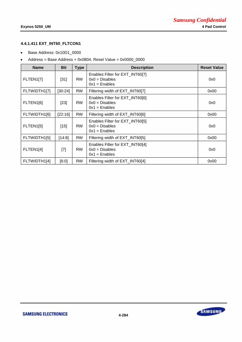
Samsung Confidential Exynos 5250_UM 4 Pad Control
4-284
4.4.1.411 EXT_INT60_FLTCON1
Base Address: 0x10D1_0000
Address = Base Address + 0x0804, Reset Value = 0x0000_0000
Name Bit Type Description Reset Value
FLTEN1[7] [31] RW
Enables Filter for EXT_INT60[7]
0x0 = Disables
0x1 = Enables
0x0
FLTWIDTH1[7] [30:24] RW Filtering width of EXT_INT60[7] 0x00
FLTEN1[6] [23] RW
Enables Filter for EXT_INT60[6]
0x0 = Disables
0x1 = Enables
0x0
FLTWIDTH1[6] [22:16] RW Filtering width of EXT_INT60[6] 0x00
FLTEN1[5] [15] RW
Enables Filter for EXT_INT60[5]
0x0 = Disables
0x1 = Enables
0x0
FLTWIDTH1[5] [14:8] RW Filtering width of EXT_INT60[5] 0x00
FLTEN1[4] [7] RW
Enables Filter for EXT_INT60[4]
0x0 = Disables
0x1 = Enables
0x0
FLTWIDTH1[4] [6:0] RW Filtering width of EXT_INT60[4] 0x00

Samsung Confidential Exynos 5250_UM 4 Pad Control
4-285
4.4.1.412 EXT_INT61_FLTCON0
Base Address: 0x10D1_0000
Address = Base Address + 0x0808, Reset Value = 0x0000_0000
Name Bit Type Description Reset Value
FLTEN2[3] [31] RW
Enables Filter for EXT_INT61[3]
0x0 = Disables
0x1 = Enables
0x0
FLTWIDTH2[3] [30:24] RW Filtering width of EXT_INT61[3] 0x00
FLTEN2[2] [23] RW
Enables Filter for EXT_INT61[2]
0x0 = Disables
0x1 = Enables
0x0
FLTWIDTH2[2] [22:16] RW Filtering width of EXT_INT61[2] 0x00
FLTEN2[1] [15] RW
Enables Filter for EXT_INT61[1]
0x0 = Disables
0x1 = Enables
0x0
FLTWIDTH2[1] [14:8] RW Filtering width of EXT_INT61[1] 0x00
FLTEN2[0] [7] RW
Enables Filter for EXT_INT61[0]
0x0 = Disables
0x1 = Enables
0x0
FLTWIDTH2[0] [6:0] RW Filtering width of EXT_INT61[0] 0x00

Samsung Confidential Exynos 5250_UM 4 Pad Control
4-286
4.4.1.413 EXT_INT61_FLTCON1
Base Address: 0x10D1_0000
Address = Base Address + 0x080C, Reset Value = 0x0000_0000
Name Bit Type Description Reset Value
FLTEN2[7] [31] RW
Enables Filter for EXT_INT61[7]
0x0 = Disables
0x1 = Enables
0x0
FLTWIDTH2[7] [30:24] RW Filtering width of EXT_INT61[7] 0x00
FLTEN2[6] [23] RW
Enables Filter for EXT_INT61[6]
0x0 = Disables
0x1 = Enables
0x0
FLTWIDTH2[6] [22:16] RW Filtering width of EXT_INT61[6] 0x00
FLTEN2[5] [15] RW
Enables Filter for EXT_INT61[5]
0x0 = Disables
0x1 = Enables
0x0
FLTWIDTH2[5] [14:8] RW Filtering width of EXT_INT61[5] 0x00
FLTEN2[4] [7] RW
Enables Filter for EXT_INT61[4]
0x0 = Disables
0x1 = Enables
0x0
FLTWIDTH2[4] [6:0] RW Filtering width of EXT_INT61[4] 0x00

Samsung Confidential Exynos 5250_UM 4 Pad Control
4-287
4.4.1.414 EXT_INT62_FLTCON0
Base Address: 0x10D1_0000
Address = Base Address + 0x0810, Reset Value = 0x0000_0000
Name Bit Type Description Reset Value
FLTEN3[3] [31] RW
Enables Filter for EXT_INT62[3]
0x0 = Disables
0x1 = Enables
0x0
FLTWIDTH3[3] [30:24] RW Filtering width of EXT_INT62[3] 0x00
FLTEN3[2] [23] RW
Enables Filter for EXT_INT62[2]
0x0 = Disables
0x1 = Enables
0x0
FLTWIDTH3[2] [22:16] RW Filtering width of EXT_INT62[2] 0x00
FLTEN3[1] [15] RW
Enables Filter for EXT_INT62[1]
0x0 = Disables
0x1 = Enables
0x0
FLTWIDTH3[1] [14:8] RW Filtering width of EXT_INT62[1] 0x00
FLTEN3[0] [7] RW
Enables Filter for EXT_INT62[0]
0x0 = Disables
0x1 = Enables
0x0
FLTWIDTH3[0] [6:0] RW Filtering width of EXT_INT62[0] 0x00

Samsung Confidential Exynos 5250_UM 4 Pad Control
4-288
4.4.1.415 EXT_INT62_FLTCON1
Base Address: 0x10D1_0000
Address = Base Address + 0x0814, Reset Value = 0x0000_0000
Name Bit Type Description Reset Value
FLTEN3[7] [31] RW
Enables Filter for EXT_INT62[7]
0x0 = Disables
0x1 = Enables
0x0
FLTWIDTH3[7] [30:24] RW Filtering width of EXT_INT62[7] 0x00
FLTEN3[6] [23] RW
Enables Filter for EXT_INT62[6]
0x0 = Disables
0x1 = Enables
0x0
FLTWIDTH3[6] [22:16] RW Filtering width of EXT_INT62[6] 0x00
FLTEN3[5] [15] RW
Enables Filter for EXT_INT62[5]
0x0 = Disables
0x1 = Enables
0x0
FLTWIDTH3[5] [14:8] RW Filtering width of EXT_INT62[5] 0x00
FLTEN3[4] [7] RW
Enables Filter for EXT_INT62[4]
0x0 = Disables
0x1 = Enables
0x0
FLTWIDTH3[4] [6:0] RW Filtering width of EXT_INT62[4] 0x00

Samsung Confidential Exynos 5250_UM 4 Pad Control
4-289
4.4.1.416 EXT_INT63_FLTCON0
Base Address: 0x10D1_0000
Address = Base Address + 0x0818, Reset Value = 0x0000_0000
Name Bit Type Description Reset Value
FLTEN4[3] [31] RW
Enables Filter for EXT_INT63[3]
0x0 = Disables
0x1 = Enables
0x0
FLTWIDTH4[3] [30:24] RW Filtering width of EXT_INT63[3] 0x00
FLTEN4[2] [23] RW
Enables Filter for EXT_INT63[2]
0x0 = Disables
0x1 = Enables
0x0
FLTWIDTH4[2] [22:16] RW Filtering width of EXT_INT63[2] 0x00
FLTEN4[1] [15] RW
Enables Filter for EXT_INT63[1]
0x0 = Disables
0x1 = Enables
0x0
FLTWIDTH4[1] [14:8] RW Filtering width of EXT_INT63[1] 0x00
FLTEN4[0] [7] RW
Enables Filter for EXT_INT63[0]
0x0 = Disables
0x1 = Enables
0x0
FLTWIDTH4[0] [6:0] RW Filtering width of EXT_INT63[0] 0x00

Samsung Confidential Exynos 5250_UM 4 Pad Control
4-290
4.4.1.417 EXT_INT63_FLTCON1
Base Address: 0x10D1_0000
Address = Base Address + 0x081C, Reset Value = 0x0000_0000
Name Bit Type Description Reset Value
FLTEN4[7] [31] RW
Enables Filter for EXT_INT63[7]
0x0 = Disables
0x1 = Enables
0x0
FLTWIDTH4[7] [30:24] RW Filtering width of EXT_INT63[7] 0x00
FLTEN4[6] [23] RW
Enables Filter for EXT_INT63[6]
0x0 = Disables
0x1 = Enables
0x0
FLTWIDTH4[6] [22:16] RW Filtering width of EXT_INT63[6] 0x00
FLTEN4[5] [15] RW
Enables Filter for EXT_INT63[5]
0x0 = Disables
0x1 = Enables
0x0
FLTWIDTH4[5] [14:8] RW Filtering width of EXT_INT63[5] 0x00
FLTEN4[4] [7] RW
Enables Filter for EXT_INT63[4]
0x0 = Disables
0x1 = Enables
0x0
FLTWIDTH4[4] [6:0] RW Filtering width of EXT_INT63[4] 0x00

Samsung Confidential Exynos 5250_UM 4 Pad Control
4-291
4.4.1.418 EXT_INT64_FLTCON0
Base Address: 0x10D1_0000
Address = Base Address + 0x0820, Reset Value = 0x0000_0000
Name Bit Type Description Reset Value
RSVD [31:16] – Reserved 0x0000
FLTEN5[1] [15] RW
Enables Filter for EXT_INT64[1]
0x0 = Disables
0x1 = Enables
0x0
FLTWIDTH5[1] [14:8] RW Filtering width of EXT_INT64[1] 0x00
FLTEN5[0] [7] RW
Enables Filter for EXT_INT64[0]
0x0 = Disables
0x1 = Enables
0x0
FLTWIDTH5[0] [6:0] RW Filtering width of EXT_INT64[0] 0x00
4.4.1.419 EXT_INT64_FLTCON1
Base Address: 0x10D1_0000
Address = Base Address + 0x0824, Reset Value = 0x0000_0000
Name Bit Type Description Reset Value
RSVD [31:0] – Reserved 0x00000000

Samsung Confidential Exynos 5250_UM 4 Pad Control
4-292
4.4.1.420 EXT_INT60_MASK
Base Address: 0x10D1_0000
Address = Base Address + 0x0900, Reset Value = 0x0000_00FF
Name Bit Type Description Reset Value
RSVD [31:8] – Reserved 0x000000
EXT_INT60
_MASK[7] [7] RW
0x0 = Enables Interrupt
0x1 = Masks Interrupt 0x1
EXT_INT60
_MASK[6] [6] RW
0x0 = Enables Interrupt
0x1 = Masks Interrupt 0x1
EXT_INT60
_MASK[5] [5] RW
0x0 = Enables Interrupt
0x1 = Masks Interrupt 0x1
EXT_INT60
_MASK[4] [4] RW
0x0 = Enables Interrupt
0x1 = Masks Interrupt 0x1
EXT_INT60
_MASK[3] [3] RW
0x0 = Enables Interrupt
0x1 = Masks Interrupt 0x1
EXT_INT60
_MASK[2] [2] RW
0x0 = Enables Interrupt
0x1 = Masks Interrupt 0x1
EXT_INT60
_MASK[1] [1] RW
0x0 = Enables Interrupt
0x1 = Masks Interrupt 0x1
EXT_INT60
_MASK[0] [0] RW
0x0 = Enables Interrupt
0x1 = Masks Interrupt 0x1

Samsung Confidential Exynos 5250_UM 4 Pad Control
4-293
4.4.1.421 EXT_INT61_MASK
Base Address: 0x10D1_0000
Address = Base Address + 0x0904, Reset Value = 0x0000_00FF
Name Bit Type Description Reset Value
RSVD [31:8] – Reserved 0x000000
EXT_INT61
_MASK[7] [7] RW
0x0 = Enables Interrupt
0x1 = Masks Interrupt 0x1
EXT_INT61
_MASK[6] [6] RW
0x0 = Enables Interrupt
0x1 = Masks Interrupt 0x1
EXT_INT61
_MASK[5] [5] RW
0x0 = Enables Interrupt
0x1 = Masks Interrupt 0x1
EXT_INT61
_MASK[4] [4] RW
0x0 = Enables Interrupt
0x1 = Masks Interrupt 0x1
EXT_INT61
_MASK[3] [3] RW
0x0 = Enables Interrupt
0x1 = Masks Interrupt 0x1
EXT_INT61
_MASK[2] [2] RW
0x0 = Enables Interrupt
0x1 = Masks Interrupt 0x1
EXT_INT61
_MASK[1] [1] RW
0x0 = Enables Interrupt
0x1 = Masks Interrupt 0x1
EXT_INT61
_MASK[0] [0] RW
0x0 = Enables Interrupt
0x1 = Masks Interrupt 0x1

Samsung Confidential Exynos 5250_UM 4 Pad Control
4-294
4.4.1.422 EXT_INT62_MASK
Base Address: 0x10D1_0000
Address = Base Address + 0x0908, Reset Value = 0x0000_00FF
Name Bit Type Description Reset Value
RSVD [31:8] – Reserved 0x000000
EXT_INT62
_MASK[7] [7] RW
0x0 = Enables Interrupt
0x1 = Masks Interrupt 0x1
EXT_INT62
_MASK[6] [6] RW
0x0 = Enables Interrupt
0x1 = Masks Interrupt 0x1
EXT_INT62
_MASK[5] [5] RW
0x0 = Enables Interrupt
0x1 = Masks Interrupt 0x1
EXT_INT62
_MASK[4] [4] RW
0x0 = Enables Interrupt
0x1 = Masks Interrupt 0x1
EXT_INT62
_MASK[3] [3] RW
0x0 = Enables Interrupt
0x1 = Masks Interrupt 0x1
EXT_INT62
_MASK[2] [2] RW
0x0 = Enables Interrupt
0x1 = Masks Interrupt 0x1
EXT_INT62
_MASK[1] [1] RW
0x0 = Enables Interrupt
0x1 = Masks Interrupt 0x1
EXT_INT62
_MASK[0] [0] RW
0x0 = Enables Interrupt
0x1 = Masks Interrupt 0x1

Samsung Confidential Exynos 5250_UM 4 Pad Control
4-295
4.4.1.423 EXT_INT63_MASK
Base Address: 0x10D1_0000
Address = Base Address + 0x090C, Reset Value = 0x0000_00FF
Name Bit Type Description Reset Value
RSVD [31:8] – Reserved 0x000000
EXT_INT63
_MASK[7] [7] RW
0x0 = Enables Interrupt
0x1 = Masks Interrupt 0x1
EXT_INT63
_MASK[6] [6] RW
0x0 = Enables Interrupt
0x1 = Masks Interrupt 0x1
EXT_INT63
_MASK[5] [5] RW
0x0 = Enables Interrupt
0x1 = Masks Interrupt 0x1
EXT_INT63
_MASK[4] [4] RW
0x0 = Enables Interrupt
0x1 = Masks Interrupt 0x1
EXT_INT63
_MASK[3] [3] RW
0x0 = Enables Interrupt
0x1 = Masks Interrupt 0x1
EXT_INT63
_MASK[2] [2] RW
0x0 = Enables Interrupt
0x1 = Masks Interrupt 0x1
EXT_INT63
_MASK[1] [1] RW
0x0 = Enables Interrupt
0x1 = Masks Interrupt 0x1
EXT_INT63
_MASK[0] [0] RW
0x0 = Enables Interrupt
0x1 = Masks Interrupt 0x1

Samsung Confidential Exynos 5250_UM 4 Pad Control
4-296
4.4.1.424 EXT_INT64_MASK
Base Address: 0x10D1_0000
Address = Base Address + 0x0910, Reset Value = 0x0000_0003
Name Bit Type Description Reset Value
RSVD [31:2] – Reserved 0x00000000
EXT_INT64
_MASK[1] [1] RW
0x0 = Enables Interrupt
0x1 = Masks Interrupt 0x1
EXT_INT64
_MASK[0] [0] RW
0x0 = Enables Interrupt
0x1 = Masks Interrupt 0x1
4.4.1.425 EXT_INT60_PEND
Base Address: 0x10D1_0000
Address = Base Address + 0x0A00, Reset Value = 0x0000_0000
Name Bit Type Description Reset Value
RSVD [31:8] – Reserved 0x000000
EXT_INT60
_PEND[7] [7] RWX
0x0 = Does not occur
0x1 = Interrupt occurs 0x0
EXT_INT60
_PEND[6] [6] RWX
0x0 = Does not occur
0x1 = Interrupt occurs 0x0
EXT_INT60
_PEND[5] [5] RWX
0x0 = Does not occur
0x1 = Interrupt occurs 0x0
EXT_INT60
_PEND[4] [4] RWX
0x0 = Does not occur
0x1 = Interrupt occurs 0x0
EXT_INT60
_PEND[3] [3] RWX
0x0 = Does not occur
0x1 = Interrupt occurs 0x0
EXT_INT60
_PEND[2] [2] RWX
0x0 = Does not occur
0x1 = Interrupt occurs 0x0
EXT_INT60
_PEND[1] [1] RWX
0x0 = Does not occur
0x1 = Interrupt occurs 0x0
EXT_INT60
_PEND[0] [0] RWX
0x0 = Does not occur
0x1 = Interrupt occurs 0x0

Samsung Confidential Exynos 5250_UM 4 Pad Control
4-297
4.4.1.426 EXT_INT61_PEND
Base Address: 0x10D1_0000
Address = Base Address + 0x0A04, Reset Value = 0x0000_0000
Name Bit Type Description Reset Value
RSVD [31:8] – Reserved 0x000000
EXT_INT61
_PEND[7] [7] RWX
0x0 = Does not occur
0x1 = Interrupt occurs 0x0
EXT_INT61
_PEND[6] [6] RWX
0x0 = Does not occur
0x1 = Interrupt occurs 0x0
EXT_INT61
_PEND[5] [5] RWX
0x0 = Does not occur
0x1 = Interrupt occurs 0x0
EXT_INT61
_PEND[4] [4] RWX
0x0 = Does not occur
0x1 = Interrupt occurs 0x0
EXT_INT61
_PEND[3] [3] RWX
0x0 = Does not occur
0x1 = Interrupt occurs 0x0
EXT_INT61
_PEND[2] [2] RWX
0x0 = Does not occur
0x1 = Interrupt occurs 0x0
EXT_INT61
_PEND[1] [1] RWX
0x0 = Does not occur
0x1 = Interrupt occurs 0x0
EXT_INT61
_PEND[0] [0] RWX
0x0 = Does not occur
0x1 = Interrupt occurs 0x0

Samsung Confidential Exynos 5250_UM 4 Pad Control
4-298
4.4.1.427 EXT_INT62_PEND
Base Address: 0x10D1_0000
Address = Base Address + 0x0A08, Reset Value = 0x0000_0000
Name Bit Type Description Reset Value
RSVD [31:8] – Reserved 0x000000
EXT_INT62
_PEND[7] [7] RWX
0x0 = Does not occur
0x1 = Interrupt occurs 0x0
EXT_INT62
_PEND[6] [6] RWX
0x0 = Does not occur
0x1 = Interrupt occurs 0x0
EXT_INT62
_PEND[5] [5] RWX
0x0 = Does not occur
0x1 = Interrupt occurs 0x0
EXT_INT62
_PEND[4] [4] RWX
0x0 = Does not occur
0x1 = Interrupt occurs 0x0
EXT_INT62
_PEND[3] [3] RWX
0x0 = Does not occur
0x1 = Interrupt occurs 0x0
EXT_INT62
_PEND[2] [2] RWX
0x0 = Does not occur
0x1 = Interrupt occurs 0x0
EXT_INT62
_PEND[1] [1] RWX
0x0 = Does not occur
0x1 = Interrupt occurs 0x0
EXT_INT62
_PEND[0] [0] RWX
0x0 = Does not occur
0x1 = Interrupt occurs 0x0
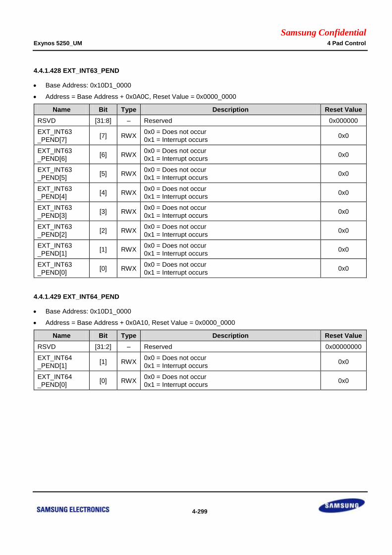
Samsung Confidential Exynos 5250_UM 4 Pad Control
4-299
4.4.1.428 EXT_INT63_PEND
Base Address: 0x10D1_0000
Address = Base Address + 0x0A0C, Reset Value = 0x0000_0000
Name Bit Type Description Reset Value
RSVD [31:8] – Reserved 0x000000
EXT_INT63
_PEND[7] [7] RWX
0x0 = Does not occur
0x1 = Interrupt occurs 0x0
EXT_INT63
_PEND[6] [6] RWX
0x0 = Does not occur
0x1 = Interrupt occurs 0x0
EXT_INT63
_PEND[5] [5] RWX
0x0 = Does not occur
0x1 = Interrupt occurs 0x0
EXT_INT63
_PEND[4] [4] RWX
0x0 = Does not occur
0x1 = Interrupt occurs 0x0
EXT_INT63
_PEND[3] [3] RWX
0x0 = Does not occur
0x1 = Interrupt occurs 0x0
EXT_INT63
_PEND[2] [2] RWX
0x0 = Does not occur
0x1 = Interrupt occurs 0x0
EXT_INT63
_PEND[1] [1] RWX
0x0 = Does not occur
0x1 = Interrupt occurs 0x0
EXT_INT63
_PEND[0] [0] RWX
0x0 = Does not occur
0x1 = Interrupt occurs 0x0
4.4.1.429 EXT_INT64_PEND
Base Address: 0x10D1_0000
Address = Base Address + 0x0A10, Reset Value = 0x0000_0000
Name Bit Type Description Reset Value
RSVD [31:2] – Reserved 0x00000000
EXT_INT64
_PEND[1] [1] RWX
0x0 = Does not occur
0x1 = Interrupt occurs 0x0
EXT_INT64
_PEND[0] [0] RWX
0x0 = Does not occur
0x1 = Interrupt occurs 0x0
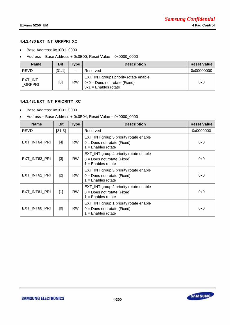
Samsung Confidential Exynos 5250_UM 4 Pad Control
4-300
4.4.1.430 EXT_INT_GRPPRI_XC
Base Address: 0x10D1_0000
Address = Base Address + 0x0B00, Reset Value = 0x0000_0000
Name Bit Type Description Reset Value
RSVD [31:1] – Reserved 0x00000000
EXT_INT
_GRPPRI [0] RW
EXT_INT groups priority rotate enable
0x0 = Does not rotate (Fixed)
0x1 = Enables rotate
0x0
4.4.1.431 EXT_INT_PRIORITY_XC
Base Address: 0x10D1_0000
Address = Base Address + 0x0B04, Reset Value = 0x0000_0000
Name Bit Type Description Reset Value
RSVD [31:5] – Reserved 0x0000000
EXT_INT64_PRI [4] RW
EXT_INT group 5 priority rotate enable
0 = Does not rotate (Fixed)
1 = Enables rotate
0x0
EXT_INT63_PRI [3] RW
EXT_INT group 4 priority rotate enable
0 = Does not rotate (Fixed)
1 = Enables rotate
0x0
EXT_INT62_PRI [2] RW
EXT_INT group 3 priority rotate enable
0 = Does not rotate (Fixed)
1 = Enables rotate
0x0
EXT_INT61_PRI [1] RW
EXT_INT group 2 priority rotate enable
0 = Does not rotate (Fixed)
1 = Enables rotate
0x0
EXT_INT60_PRI [0] RW
EXT_INT group 1 priority rotate enable
0 = Does not rotate (Fixed)
1 = Enables rotate
0x0

Samsung Confidential Exynos 5250_UM 4 Pad Control
4-301
4.4.1.432 EXT_INT_SERVICE_XC
Base Address: 0x10D1_0000
Address = Base Address + 0x0B08, Reset Value = 0x0000_0000
Name Bit Type Description Reset Value
RSVD [31:8] RW Reserved 0x0000000
SVC_Group
_Num [7:3] RW EXT_INT Service group number 0x00
SVC_Num [2:0] RW Services this Interrupt number 0x0
4.4.1.433 EXT_INT_SERVICE_PEND_XC
Base Address: 0x10D1_0000
Address = Base Address + 0x0B0C, Reset Value = 0x0000_0000
Name Bit Type Description Reset Value
RSVD [31:8] RW Reserved 0x0000000
SVC_PEND [7:0] RW 0x0 = Does not occur
0x1 = Interrupt occurs 0x00
4.4.1.434 EXT_INT_GRPFIXPRI_XC
Base Address: 0x10D1_0000
Address = Base Address + 0x0B10, Reset Value = 0x0000_0000
Name Bit Type Description Reset Value
RSVD [31:5] – Reserved 0x0000000
Highest_GRP
_NUM [4:0] RW
Group number of the highest priority when fixed group
priority mode: 1 to 25 0x00

Samsung Confidential Exynos 5250_UM 4 Pad Control
4-302
4.4.1.435 EXT_INT60_FIXPRI
Base Address: 0x10D1_0000
Address = Base Address + 0x0B14, Reset Value = 0x0000_0000
Name Bit Type Description Reset Value
RSVD [31:3] – Reserved 0x00000000
Highest_EINT
_NUM [2:0] RW
Interrupt number of the highest priority in External Interrupt
Group 1 (EXT_INT60) when fixed priority mode: 0 to 7 0x0
4.4.1.436 EXT_INT61_FIXPRI
Base Address: 0x10D1_0000
Address = Base Address + 0x0B18, Reset Value = 0x0000_0000
Name Bit Type Description Reset Value
RSVD [31:3] – Reserved 0x00000000
Highest_EINT
_NUM [2:0] RW
Interrupt number of the highest priority in External Interrupt
Group 2 (EXT_INT61) when fixed priority mode: 0 to 7 0x0
4.4.1.437 EXT_INT62_FIXPRI
Base Address: 0x10D1_0000
Address = Base Address + 0x0B1C, Reset Value = 0x0000_0000
Name Bit Type Description Reset Value
RSVD [31:3] – Reserved 0x00000000
Highest_EINT
_NUM [2:0] RW
Interrupt number of the highest priority in External Interrupt
Group 3 (EXT_INT62) when fixed priority mode: 0 to 7 0x0
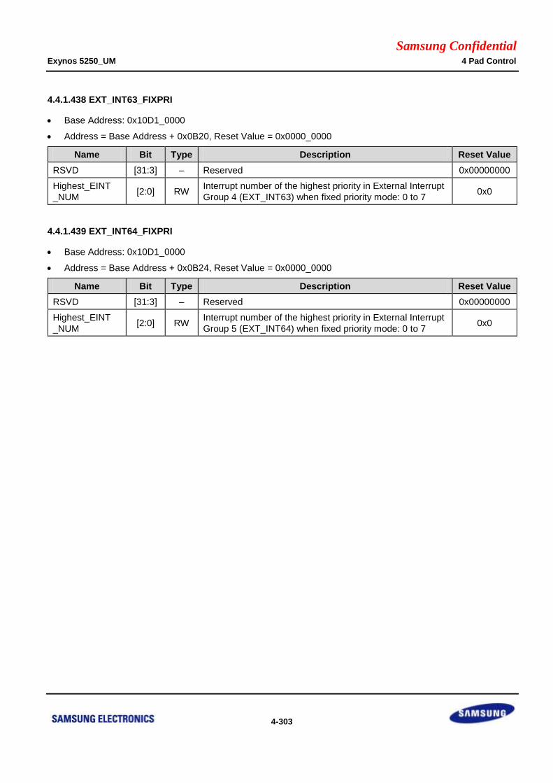
Samsung Confidential Exynos 5250_UM 4 Pad Control
4-303
4.4.1.438 EXT_INT63_FIXPRI
Base Address: 0x10D1_0000
Address = Base Address + 0x0B20, Reset Value = 0x0000_0000
Name Bit Type Description Reset Value
RSVD [31:3] – Reserved 0x00000000
Highest_EINT
_NUM [2:0] RW
Interrupt number of the highest priority in External Interrupt
Group 4 (EXT_INT63) when fixed priority mode: 0 to 7 0x0
4.4.1.439 EXT_INT64_FIXPRI
Base Address: 0x10D1_0000
Address = Base Address + 0x0B24, Reset Value = 0x0000_0000
Name Bit Type Description Reset Value
RSVD [31:3] – Reserved 0x00000000
Highest_EINT
_NUM [2:0] RW
Interrupt number of the highest priority in External Interrupt
Group 5 (EXT_INT64) when fixed priority mode: 0 to 7 0x0
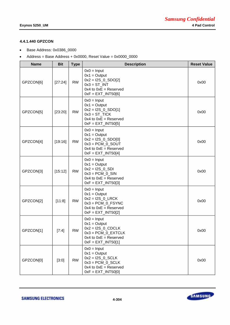
Samsung Confidential Exynos 5250_UM 4 Pad Control
4-304
4.4.1.440 GPZCON
Base Address: 0x0386_0000
Address = Base Address + 0x0000, Reset Value = 0x0000_0000
Name Bit Type Description Reset Value
GPZCON[6] [27:24] RW
0x0 = Input
0x1 = Output
0x2 = I2S_0_SDO[2]
0x3 = ST_INT
0x4 to 0xE = Reserved
0xF = EXT_INT50[6]
0x00
GPZCON[5] [23:20] RW
0x0 = Input
0x1 = Output
0x2 = I2S_0_SDO[1]
0x3 = ST_TICK
0x4 to 0xE = Reserved
0xF = EXT_INT50[5]
0x00
GPZCON[4] [19:16] RW
0x0 = Input
0x1 = Output
0x2 = I2S_0_SDO[0]
0x3 = PCM_0_SOUT
0x4 to 0xE = Reserved
0xF = EXT_INT50[4]
0x00
GPZCON[3] [15:12] RW
0x0 = Input
0x1 = Output
0x2 = I2S_0_SDI
0x3 = PCM_0_SIN
0x4 to 0xE = Reserved
0xF = EXT_INT50[3]
0x00
GPZCON[2] [11:8] RW
0x0 = Input
0x1 = Output
0x2 = I2S_0_LRCK
0x3 = PCM_0_FSYNC
0x4 to 0xE = Reserved
0xF = EXT_INT50[2]
0x00
GPZCON[1] [7:4] RW
0x0 = Input
0x1 = Output
0x2 = I2S_0_CDCLK
0x3 = PCM_0_EXTCLK
0x4 to 0xE = Reserved
0xF = EXT_INT50[1]
0x00
GPZCON[0] [3:0] RW
0x0 = Input
0x1 = Output
0x2 = I2S_0_SCLK
0x3 = PCM_0_SCLK
0x4 to 0xE = Reserved
0xF = EXT_INT50[0]
0x00

Samsung Confidential Exynos 5250_UM 4 Pad Control
4-305
4.4.1.441 GPZDAT
Base Address: 0x0386_0000
Address = Base Address + 0x0004, Reset Value = 0x00
Name Bit Type Description Reset Value
GPZDAT[6:0] [6:0] RWX
When you configure the port as input port, the
corresponding bit is the pin state. When you configure
the port as output port, the pin state is the same as the
corresponding bit. When you configure the port as
functional pin, the undefined value will be read.
0x00
4.4.1.442 GPZPUD
Base Address: 0x0386_0000
Address = Base Address + 0x0008, Reset Value = 0x1555
Name Bit Type Description Reset Value
GPZPUD[n] [2n + 1:2n]
n = 0 to 6 RW
0x0 = Disables Pull-up/down
0x1 = Enables Pull-down
0x2 = Reserved
0x3 = Enables Pull-up
0x1555
4.4.1.443 GPZDRV
Base Address: 0x0386_0000
Address = Base Address + 0x000C, Reset Value = 0x00_0000
Name Bit Type Description Reset Value
GPZDRV[n]
[2n + 1:2n]
N = 0 to 6 RW
0x0 = 1x
0x2 = 2x
0x1 = 3x
0x3 = 4x
0x00_0000
[n + 16:16]
n = 0 to 6 RW Reserved. Should be zero. 0x00_0000

Samsung Confidential Exynos 5250_UM 4 Pad Control
4-306
4.4.1.444 GPZCONPDN
Base Address: 0x0386_0000
Address = Base Address + 0x0010, Reset Value = 0x0000
Name Bit Type Description Reset Value
GPZ[n] [2n + 1:2n]
n = 0 to 6 RW
0x0 = Output 0
0x1 = Output 1
0x2 = Input
0x3 = Previous state
0x00
4.4.1.445 GPZPUDPDN
Base Address: 0x0386_0000
Address = Base Address + 0x0014, Reset Value = 0x0000
Name Bit Type Description Reset Value
GPZ[n] [2n + 1:2n]
n = 0 to 6 RW
0x0 = Disables Pull-up/down
0x1 = Enables Pull-down
0x2 = Reserved
0x3 = Enables Pull-up
0x00

Samsung Confidential Exynos 5250_UM 4 Pad Control
4-307
4.4.1.446 EXT_INT50CON
Base Address: 0x0386_0000
Address = Base Address + 0x0700, Reset Value = 0x0000_0000
Name Bit Type Description Reset Value
RSVD [31:28] – Reserved 0x0
RSVD [27] – Reserved 0x0
EXT_INT50
_CON[6] [26:24] RW
Setting the signaling method of EXT_INT50[6]
0x0 = Sets Low level
0x1 = Sets High level
0x2 = Triggers Falling edge
0x3 = Triggers Rising edge
0x4 = Triggers Both edge
0x5 to 0x7 = Reserved
0x0
RSVD [23] – Reserved 0x0
EXT_INT50
_CON[5] [22:20] RW
Setting the signaling method of EXT_INT50[5]
0x0 = Sets Low level
0x1 = Sets High level
0x2 = Triggers Falling edge
0x3 = Triggers Rising edge
0x4 = Triggers Both edge
0x5 to 0x7 = Reserved
0x0
RSVD [19] – Reserved 0x0
EXT_INT50
_CON[4] [18:16] RW
Setting the signaling method of EXT_INT50[4]
0x0 = Sets Low level
0x1 = Sets High level
0x2 = Triggers Falling edge
0x3 = Triggers Rising edge
0x4 = Triggers Both edge
0x5 to 0x7 = Reserved
0x0
RSVD [15] – Reserved 0x0
EXT_INT50
_CON[3] [14:12] RW
Setting the signaling method of EXT_INT50[3]
0x0 = Sets Low level
0x1 = Sets High level
0x2 = Triggers Falling edge
0x3 = Triggers Rising edge
0x4 = Triggers Both edge
0x5 to 0x7 = Reserved
0x0
RSVD [11] – Reserved 0x0
EXT_INT50
_CON[2] [10:8] RW
Setting the signaling method of EXT_INT50[2]
0x0 = Sets Low level
0x1 = Sets High level
0x2 = Triggers Falling edge
0x3 = Triggers Rising edge
0x4 = Triggers Both edge
0x5 to 0x7 = Reserved
0x0
RSVD [7] – Reserved 0x0

Samsung Confidential Exynos 5250_UM 4 Pad Control
4-308
Name Bit Type Description Reset Value
EXT_INT50
_CON[1] [6:4] RW
Setting the signaling method of EXT_INT50[1]
0x0 = Sets Low level
0x1 = Sets High level
0x2 = Triggers Falling edge
0x3 = Triggers Rising edge
0x4 = Triggers Both edge
0x5 to 0x7 = Reserved
0x0
RSVD [3] – Reserved 0x0
EXT_INT50
_CON[0] [2:0] RW
Setting the signaling method of EXT_INT50[0]
0x0 = Sets Low level
0x1 = Sets High level
0x2 = Triggers Falling edge
0x3 = Triggers Rising edge
0x4 = Triggers Both edge
0x5 to 0x7 = Reserved
0x0

Samsung Confidential Exynos 5250_UM 4 Pad Control
4-309
4.4.1.447 EXT_INT50_FLTCON0
Base Address: 0x0386_0000
Address = Base Address + 0x0800, Reset Value = 0x0000_0000
Name Bit Type Description Reset Value
FLTEN1[3] [31] RW
Enables Filter for EXT_INT50[3]
0x0 = Disables
0x1 = Enables
0x0
FLTWIDTH1[3] [30:24] RW Filtering width of EXT_INT50[3] 0x00
FLTEN1[2] [23] RW
Enables Filter for EXT_INT50[2]
0x0 = Disables
0x1 = Enables
0x0
FLTWIDTH1[2] [22:16] RW Filtering width of EXT_INT50[2] 0x00
FLTEN1[1] [15] RW
Enables Filter for EXT_INT50[1]
0x0 = Disables
0x1 = Enables
0x0
FLTWIDTH1[1] [14:8] RW Filtering width of EXT_INT50[1] 0x00
FLTEN1[0] [7] RW
Enables Filter for EXT_INT50[0]
0x0 = Disables
0x1 = Enables
0x0
FLTWIDTH1[0] [6:0] RW Filtering width of EXT_INT50[0] 0x00
4.4.1.448 EXT_INT50_FLTCON1
Base Address: 0x0386_0000
Address = Base Address + 0x0804, Reset Value = 0x0000_0000
Name Bit Type Description Reset Value
RSVD [31:24] – Reserved 0x00
FLTEN1[6] [23] RW
Enables Filter for EXT_INT50[6]
0x0 = Disables
0x1 = Enables
0x0
FLTWIDTH1[6] [22:16] RW Filtering width of EXT_INT50[6] 0x00
FLTEN1[5] [15] RW
Enables Filter for EXT_INT50[5]
0x0 = Disables
0x1 = Enables
0x0
FLTWIDTH1[5] [14:8] RW Filtering width of EXT_INT50[5] 0x00
FLTEN1[4] [7] RW
Enables Filter for EXT_INT50[4]
0x0 = Disables
0x1 = Enables
0x0
FLTWIDTH1[4] [6:0] RW Filtering width of EXT_INT50[4] 0x00

Samsung Confidential Exynos 5250_UM 4 Pad Control
4-310
4.4.1.449 EXT_INT50_MASK
Base Address: 0x0386_0000
Address = Base Address + 0x0900, Reset Value = 0x0000_007F
Name Bit Type Description Reset Value
RSVD [31:7] – Reserved 0x0000000
EXT_INT50
_MASK[6] [6] RW
0x0 = Enables Interrupt
0x1 = Masks Interrupt 0x1
EXT_INT50
_MASK[5] [5] RW
0x0 = Enables Interrupt
0x1 = Masks Interrupt 0x1
EXT_INT50
_MASK[4] [4] RW
0x0 = Enables Interrupt
0x1 = Masks Interrupt 0x1
EXT_INT50
_MASK[3] [3] RW
0x0 = Enables Interrupt
0x1 = Masks Interrupt 0x1
EXT_INT50
_MASK[2] [2] RW
0x0 = Enables Interrupt
0x1 = Masks Interrupt 0x1
EXT_INT50
_MASK[1] [1] RW
0x0 = Enables Interrupt
0x1 = Masks Interrupt 0x1
EXT_INT50
_MASK[0] [0] RW
0x0 = Enables Interrupt
0x1 = Masks Interrupt 0x1
4.4.1.450 EXT_INT50_PEND
Base Address: 0x0386_0000
Address = Base Address + 0x0A00, Reset Value = 0x0000_0000
Name Bit Type Description Reset Value
RSVD [31:7] – Reserved 0x0000000
EXT_INT50
_PEND[6] [6] RWX
0x0 = Does not occur
0x1 = Interrupt occurs 0x0
EXT_INT50
_PEND[5] [5] RWX
0x0 = Does not occur
0x1 = Interrupt occurs 0x0
EXT_INT50
_PEND[4] [4] RWX
0x0 = Does not occur
0x1 = Interrupt occurs 0x0
EXT_INT50
_PEND[3] [3] RWX
0x0 = Does not occur
0x1 = Interrupt occurs 0x0
EXT_INT50
_PEND[2] [2] RWX
0x0 = Does not occur
0x1 = Interrupt occurs 0x0
EXT_INT50
_PEND[1] [1] RWX
0x0 = Does not occur
0x1 = Interrupt occurs 0x0
EXT_INT50
_PEND[0] [0] RWX
0x0 = Does not occur
0x1 = Interrupt occurs 0x0
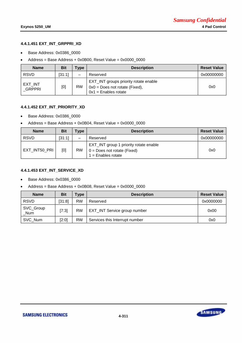
Samsung Confidential Exynos 5250_UM 4 Pad Control
4-311
4.4.1.451 EXT_INT_GRPPRI_XD
Base Address: 0x0386_0000
Address = Base Address + 0x0B00, Reset Value = 0x0000_0000
Name Bit Type Description Reset Value
RSVD [31:1] – Reserved 0x00000000
EXT_INT
_GRPPRI [0] RW
EXT_INT groups priority rotate enable
0x0 = Does not rotate (Fixed),
0x1 = Enables rotate
0x0
4.4.1.452 EXT_INT_PRIORITY_XD
Base Address: 0x0386_0000
Address = Base Address + 0x0B04, Reset Value = 0x0000_0000
Name Bit Type Description Reset Value
RSVD [31:1] – Reserved 0x00000000
EXT_INT50_PRI [0] RW
EXT_INT group 1 priority rotate enable
0 = Does not rotate (Fixed)
1 = Enables rotate
0x0
4.4.1.453 EXT_INT_SERVICE_XD
Base Address: 0x0386_0000
Address = Base Address + 0x0B08, Reset Value = 0x0000_0000
Name Bit Type Description Reset Value
RSVD [31:8] RW Reserved 0x0000000
SVC_Group
_Num [7:3] RW EXT_INT Service group number 0x00
SVC_Num [2:0] RW Services this Interrupt number 0x0
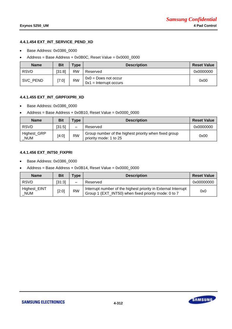
Samsung Confidential Exynos 5250_UM 4 Pad Control
4-312
4.4.1.454 EXT_INT_SERVICE_PEND_XD
Base Address: 0x0386_0000
Address = Base Address + 0x0B0C, Reset Value = 0x0000_0000
Name Bit Type Description Reset Value
RSVD [31:8] RW Reserved 0x0000000
SVC_PEND [7:0] RW 0x0 = Does not occur
0x1 = Interrupt occurs 0x00
4.4.1.455 EXT_INT_GRPFIXPRI_XD
Base Address: 0x0386_0000
Address = Base Address + 0x0B10, Reset Value = 0x0000_0000
Name Bit Type Description Reset Value
RSVD [31:5] – Reserved 0x0000000
Highest_GRP
_NUM [4:0] RW
Group number of the highest priority when fixed group
priority mode: 1 to 25 0x00
4.4.1.456 EXT_INT50_FIXPRI
Base Address: 0x0386_0000
Address = Base Address + 0x0B14, Reset Value = 0x0000_0000
Name Bit Type Description Reset Value
RSVD [31:3] – Reserved 0x00000000
Highest_EINT
_NUM [2:0] RW
Interrupt number of the highest priority in External Interrupt
Group 1 (EXT_INT50) when fixed priority mode: 0 to 7 0x0
Samsung Confidential Exynos 5250_UM 5 Clock Controller
5-1
5 Clock Controller
This chapter describes the Clock Management Units (CMUs) of Exynos 5250. These CMUs control Phase Locked
Loops (PLLs) and generate system clocks for CPU, buses, and function clocks for individual IPs in Exynos 5250.
They also communicate with Power Management Unit (PMU) to stop clocks before entering certain low power
mode. It results in reducing power consumption by minimizing clock toggling.
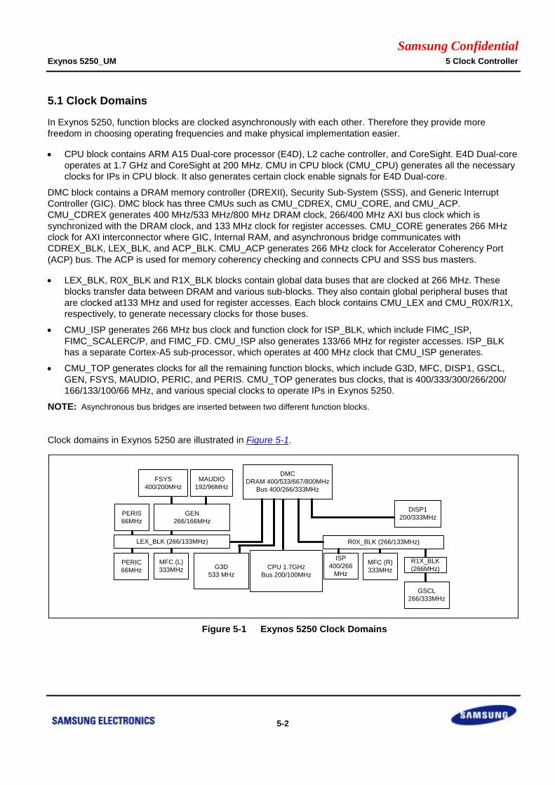
Samsung Confidential Exynos 5250_UM 5 Clock Controller
5-2
5.1 Clock Domains
In Exynos 5250, function blocks are clocked asynchronously with each other. Therefore they provide more
freedom in choosing operating frequencies and make physical implementation easier.
CPU block contains ARM A15 Dual-core processor (E4D), L2 cache controller, and CoreSight. E4D Dual-core
operates at 1.7 GHz and CoreSight at 200 MHz. CMU in CPU block (CMU_CPU) generates all the necessary
clocks for IPs in CPU block. It also generates certain clock enable signals for E4D Dual-core.
DMC block contains a DRAM memory controller (DREXII), Security Sub-System (SSS), and Generic Interrupt
Controller (GIC). DMC block has three CMUs such as CMU_CDREX, CMU_CORE, and CMU_ACP.
CMU_CDREX generates 400 MHz/533 MHz/800 MHz DRAM clock, 266/400 MHz AXI bus clock which is
synchronized with the DRAM clock, and 133 MHz clock for register accesses. CMU_CORE generates 266 MHz
clock for AXI interconnector where GIC, Internal RAM, and asynchronous bridge communicates with
CDREX_BLK, LEX_BLK, and ACP_BLK. CMU_ACP generates 266 MHz clock for Accelerator Coherency Port
(ACP) bus. The ACP is used for memory coherency checking and connects CPU and SSS bus masters.
LEX_BLK, R0X_BLK and R1X_BLK blocks contain global data buses that are clocked at 266 MHz. These
blocks transfer data between DRAM and various sub-blocks. They also contain global peripheral buses that
are clocked at133 MHz and used for register accesses. Each block contains CMU_LEX and CMU_R0X/R1X,
respectively, to generate necessary clocks for those buses.
CMU_ISP generates 266 MHz bus clock and function clock for ISP_BLK, which include FIMC_ISP,
FIMC_SCALERC/P, and FIMC_FD. CMU_ISP also generates 133/66 MHz for register accesses. ISP_BLK
has a separate Cortex-A5 sub-processor, which operates at 400 MHz clock that CMU_ISP generates.
CMU_TOP generates clocks for all the remaining function blocks, which include G3D, MFC, DISP1, GSCL,
GEN, FSYS, MAUDIO, PERIC, and PERIS. CMU_TOP generates bus clocks, that is 400/333/300/266/200/
166/133/100/66 MHz, and various special clocks to operate IPs in Exynos 5250.
NOTE: Asynchronous bus bridges are inserted between two different function blocks.
Clock domains in Exynos 5250 are illustrated in Figure 5-1.
LEX_BLK (266/133MHz) R0X_BLK (266/133MHz)
DMC
DRAM 400/533/667/800MHz
Bus 400/266/333MHz
CPU 1.7GHz
Bus 200/100MHz
PERIC
66MHz
MFC (L)
333MHz G3D
533 MHz
ISP
400/266
MHz
PERIS
66MHz
MFC (R)
333MHz
GSCL
266/333MHz
FSYS
400/200MHz
DISP1
200/333MHz
MAUDIO
192/96MHz
GEN
266/166MHz
R1X_BLK
(266MHz)
Figure 5-1 Exynos 5250 Clock Domains
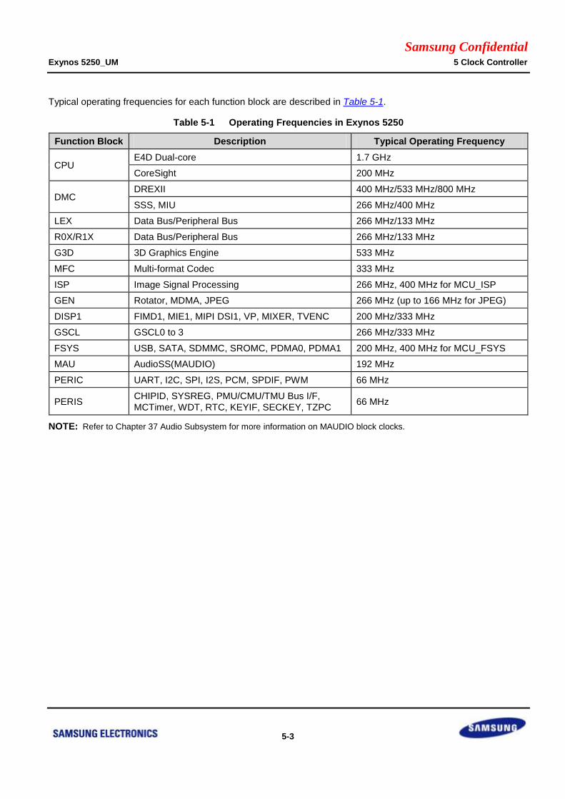
Samsung Confidential Exynos 5250_UM 5 Clock Controller
5-3
Typical operating frequencies for each function block are described in Table 5-1.
Table 5-1 Operating Frequencies in Exynos 5250
Function Block Description Typical Operating Frequency
CPU E4D Dual-core 1.7 GHz
CoreSight 200 MHz
DMC DREXII 400 MHz/533 MHz/800 MHz
SSS, MIU 266 MHz/400 MHz
LEX Data Bus/Peripheral Bus 266 MHz/133 MHz
R0X/R1X Data Bus/Peripheral Bus 266 MHz/133 MHz
G3D 3D Graphics Engine 533 MHz
MFC Multi-format Codec 333 MHz
ISP Image Signal Processing 266 MHz, 400 MHz for MCU_ISP
GEN Rotator, MDMA, JPEG 266 MHz (up to 166 MHz for JPEG)
DISP1 FIMD1, MIE1, MIPI DSI1, VP, MIXER, TVENC 200 MHz/333 MHz
GSCL GSCL0 to 3 266 MHz/333 MHz
FSYS USB, SATA, SDMMC, SROMC, PDMA0, PDMA1 200 MHz, 400 MHz for MCU_FSYS
MAU AudioSS(MAUDIO) 192 MHz
PERIC UART, I2C, SPI, I2S, PCM, SPDIF, PWM 66 MHz
PERIS CHIPID, SYSREG, PMU/CMU/TMU Bus I/F,
MCTimer, WDT, RTC, KEYIF, SECKEY, TZPC 66 MHz
NOTE: Refer to Chapter 37 Audio Subsystem for more information on MAUDIO block clocks.
Samsung Confidential Exynos 5250_UM 5 Clock Controller
5-4
5.2 Clock Declaration
The top-level clocks in Exynos 5250 are:
Clocks from clock pads, that is, XRTCXTI and XXTI.
Clocks from CMUs (for example, ARMCLK, ACLK, HCLK, and SCLK)
ARMCLK specifies clock for E4D Dual-core.
SCLK (special clock) specifies all the clocks except bus clocks and processor core clock.
Clocks from USB PHY
Clocks from GPIO pads
5.2.1 Clocks from Clock Pads
Clock pads provide these clocks.
XRTCXTI: Specifies a clock from 32.768 kHz crystal pad with XRTCXTI and XRTCXTO pins. RTC uses this
clock as the source of a real-time clock. The 10 M parallel resistance is required between XRTCXTI and
XRTCXTO.
XXTI: Specifies a clock from external oscillator with XXTI pins. XXTI use wide-range OSC pads. This clock is
supplied to APLL, MPLL, BPLL, CPLL, VPLL, EPLL, GPLL and USB PHY. Refer to Chapter 34
"USB2.0_HOST" and 35 "USB2.0_DEVICE" for more information on USB PHY clock. It is recommended to
use 24 MHz crystal because iROM was designed based on the 24 MHz input clock.
Samsung Confidential Exynos 5250_UM 5 Clock Controller
5-5
5.2.2 Clocks from CMU
CMUs generate internal clocks with intermediate frequencies using clocks from the clock pads (i.e., XRTCXTI and
XXTI), seven PLLs (i.e., APLL, MPLL, BPLL, CPLL, EPLL, GPLL and VPLL) and USB PHY and HDMI PHY
clocks. Some of these clocks can be selected, pre-scaled, and provided to the corresponding modules.
It is recommended to use 24 MHz input clock source for APLL, MPLL, BPLL, CPLL, EPLL, GPLL and VPLL.
In typical Exynos 5250 applications,
E4D Dual-core, CoreSight, and HPM use APLL
DRAM, System Bus clocks, and other peripheral clocks (for example Audio IPs and SPI) use MPLL and
EPLL.
Video clock uses VPLL
G3D uses GPLL as input clock source
MFC uses CPLL as input clock source
To generate internal clocks, these configurations are used:.
APLL uses XXTI as input and generate 22 MHz to 1.7GHz. This PLL generates 1.7 GHz clock to E4D Dual-
core CPU.
MPLL uses XXTI as input to generate 22 MHz to 1.6 GHz. This PLL generates 1.6 GHz clock to provide 400
MHz/533 MHz/800 MHz for DRAM memory controller, LPDDR Phy, and G3D. It provides 266 MHz for main
bus system.
BPLL uses XXTI as input to generate 22 MHz to 1.6 GHz. This PLL generates 1066 MHz clock to provide
533 MHz for DRAM memory controller.
CPLL uses XXTI as input to generate 333 MHz. This PLL generates 333 MHz clock to provide 333 MHz for
MFC, DISP1 and GSCLER.
EPLL uses XXTI as input to generate 22 MHz to 1.4 GHz. This PLL generates 192 MHz clock to Audio Sub-
System.
VPLL uses XXTI or SCLK_HDMI24M as input to generate 22 MHz to 1.4 GHz. This PLL generates
54 MHz video clock, 300 MHz clock to DISP1 and GSCALER.
GPLL use XXTI as input to generate 22 MHz to 1.4 GHz. This PLL generates 533 MHz to G3D.
USB Host and Device PHY use XXTI to generate 30 MHz and 48 MHz.
HDMI PHY uses XXTI to generate 54 MHz.
Clock controllers allow bypassing of PLLs for slow clock. Additionally, they can gate clocks in each block for power
reduction.
Samsung Confidential Exynos 5250_UM 5 Clock Controller
5-6
5.3 Clock Relationship
Clocks have these relationships:
CPU_BLK clocks
freq. (ARMCLK) = freq. (MOUTCPU)/n, where n = 1 to 64
freq. (ACLK_CPUD) = freq. (ARMCLK)/n, where n = 1 to 8
freq. (ACLK_ACP) = freq. (ARMCLK)/n, where n = 1 to 8
freq. (PERIPHCLK) = freq. (ARMCLK)/n, where n = 1 to 8
freq. (ATCLK) = freq. (MOUTCPU)/n, where n = 1 to 8
freq. (PCLK_DBG) = freq. (ATCLK)/n, where n = 1 to 8
DMC_BLK clocks
freq. (MCLK_CDREX) = freq. (MOUTMCLK_CDREX2)/n, where n = 1 to 8
freq. (ACLK_CDREX) = freq. (MCLK_CDREX)/n, where n = 1 to 8
freq. (MCLK_DPHY) = freq. (MOUTMCLK_DPHY)/n, where n = 1 to 8
freq. (C2C_CLK) = freq. (MOUTC2C_CLK_400)/n, where n = 1 to 8
freq. (ACLK_C2C) = freq. (C2C_CLK)/n, where n = 1 to 8
freq. (ACLK_CORED) = freq. (MOUTMPLL)/n, where n = 1 to 8
freq. (ACLK_COREP) = freq. (ACLK_CORED)/n, where n = 1 to 8
freq. (ACLK_ACP) = freq. (FOUTMPLL)/n, where n = 1 to 8
freq. (PCLK_ACP) = freq. (ACLK_ACP)/n, where n = 1 to 8
freq. (EFCLK_SYSLFT) = freq. (FOUTMPLL)/n, where n = 1 to 8
Caution: It should be guaranteed that the ratio between freq (MCLK_CDREX) and freq (ACLK_CDREX) is kept
as "2 to 1" all the time.
LEX_BLK clocks
freq. (ACLK_DLEX) = freq. (ACLK_266)/n, where n = 1 to 8
freq. (ACLK_PLEX) = freq. (ACLK_DLEX)/n, where n = 1 to 8
R0X/R1X_BLK clocks
freq. (ACLK_DR0X) = freq. (ACLK_266)/n, where n = 1 to 8
freq. (ACLK_PR0X) = freq. (ACLK_DR0X)/n, where n = 1 to 8
freq. (ACLK_DR1X) = freq. (ACLK_266)/n, where n = 1 to 8
freq. (ACLK_PR1X) = freq. (ACLK_DR1X)/n, where n = 1 to 8
Samsung Confidential Exynos 5250_UM 5 Clock Controller
5-7
CMU_TOP clocks
freq. (ACLK_400_G3D) = freq. (MOUTACLK_400_G3D)/n, where n = 1 to 8
freq. (ACLK_400_IOP) = freq. (MOUTACLK_400_IOP)/n, where n = 1 to 8
freq. (ACLK_400_ISP) = freq. (MOUTACLK_400_ISP)/n, where n = 1 to 8
freq. (ACLK_333) = freq. (MOUTACLK_333)/n, where n = 1 to 8
freq. (ACLK_300_DISP1) = freq. (MOUTACLK_300_DISP1)/n, where n = 1 to 8
freq. (ACLK_300_GSCL) = freq. (MOUTACLK_300_GSCL)/n, where n = 1 to 8
freq. (ACLK_266) = freq. (SCLKMPLL_USER)/n, where n = 1 to 8
freq. (ACLK_266_GSCL) = freq. (ACLK_266)
freq. (ACLK_266_ISP) = freq. (ACLK_266)
freq. (ACLK_200) = freq. (MOUTACLK_200)/n, where n = 1 to 8
freq. (ACLK_200_DISP1) = freq. (ACLK_200)
freq. (ACLK_MIPI_HSI_TXBASE) = freq. (MOUTACLK_MIPI_HSI_TXBASE)/n, where n = 1 to 8
freq. (ACLK_166) = freq. (MOUTACLK_166)/n, where n = 1 to 8
freq. (ACLK_66_pre) = freq. (MOUTMPLL_USER)/n, where n = 1 to 8
freq. (ACLK_66) = freq. (ACLK_66_pre)/n, where n = 1 to 8
MAU_BLK clocks
freq. (RP_CLK) = freq. (MOUTASS)/n, where n = 1 to 16
freq. (BUS_CLK) = freq. (MOUTRP)/n, where n = 1 to 16
NOTE: Clock names and clock tree diagram of MAUDIO_BLK are illustrated in Figure 34-3 of Chapter 34 Audio Subsystem.
Samsung Confidential Exynos 5250_UM 5 Clock Controller
5-8
Values for high-performance operation:
freq. (ARMCLK) = 1.7 GHz
freq. (ACLK_CPUD) = 450 MHz, 500 MHz
freq. (PERIPHCLK) = 169 MHz, 125 MHz
freq. (ATCLK) = 200 MHz
freq. (PCLK_DBG) = 100 MHz
freq. (MCLK_CDREX) = 800 MHz, 667 MHz, 533 MHz, 400 MHz
freq. (ACLK_CDREX) = 400 MHz, 333 MHz, 266 MHz, 200 MHz
freq. (PCLK_CDREX) = 133 MHz
freq. (ACLK_ACP) = 266 MHz
freq. (PCLK_ACP) = 133 MHz
freq. (ACLK_DLEX) = 266 MHz
freq. (ACLK_PLEX) = 133 MHz
freq. (ACLK_DR0X/R1X) = 266 MHz
freq. (ACLK_DR1X/R1X) = 133 MHz
freq. (ACLK_400) = 250 MHz
freq. (ACLK_400_IOP) = 400 MHz
freq. (ACLK_400_ISP) = 400 MHz
freq. (ACLK_333) = 333 MHz
freq. (ACLK_300_DISP1) = 333 MHz
freq. (ACLK_300_GSCL) = 333 MHz
freq. (ACLK_266) = 266 MHz
freq. (ACLK_266_GSCL) = 266 MHz
freq. (ACLK_266_ISP) = 266 MHz
freq. (ACLK_200) = 200 MHz
freq. (ACLK_200_DISP1) = 200 MHz
freq. (ACLK_MIPI_HSI_TXBASE) = 200 MHz
freq. (ACLK_166) = 166 MHz
freq. (ACLK_66) = 66 MHz

Samsung Confidential Exynos 5250_UM 5 Clock Controller
5-9
PLL
APLL primarily drives CPU_BLK clocks. It can generate up to 1.7 GHz.
MPLL primarily drives DMC_BLK, LEX_BLK, R0X_BLK, R1X_BLK and TOP block clocks. It can generate
up to 1.6 GHz. MPLL can also generate CPU_BLK clocks when APLL is blocked for locking during
Dynamic Voltage Frequency Scaling (DVFS).
BPLL is primarily used to generate 1066 MHz, providing 533 MHz to DMC_BLK.
CPLL is primarily used to generate 333 MHz, providing 333 MHz to MFC_BLK.
EPLL is primarily used to generate audio clock.
GPLL is primarily used to generate 533 MHz, providing 533 MHz to G3D_BLK.
VPLL is primarily used to generate video system operating clock. It uses 54 MHz and 300 MHz clock to
GSCALER_BLK and DISP1_BLK.
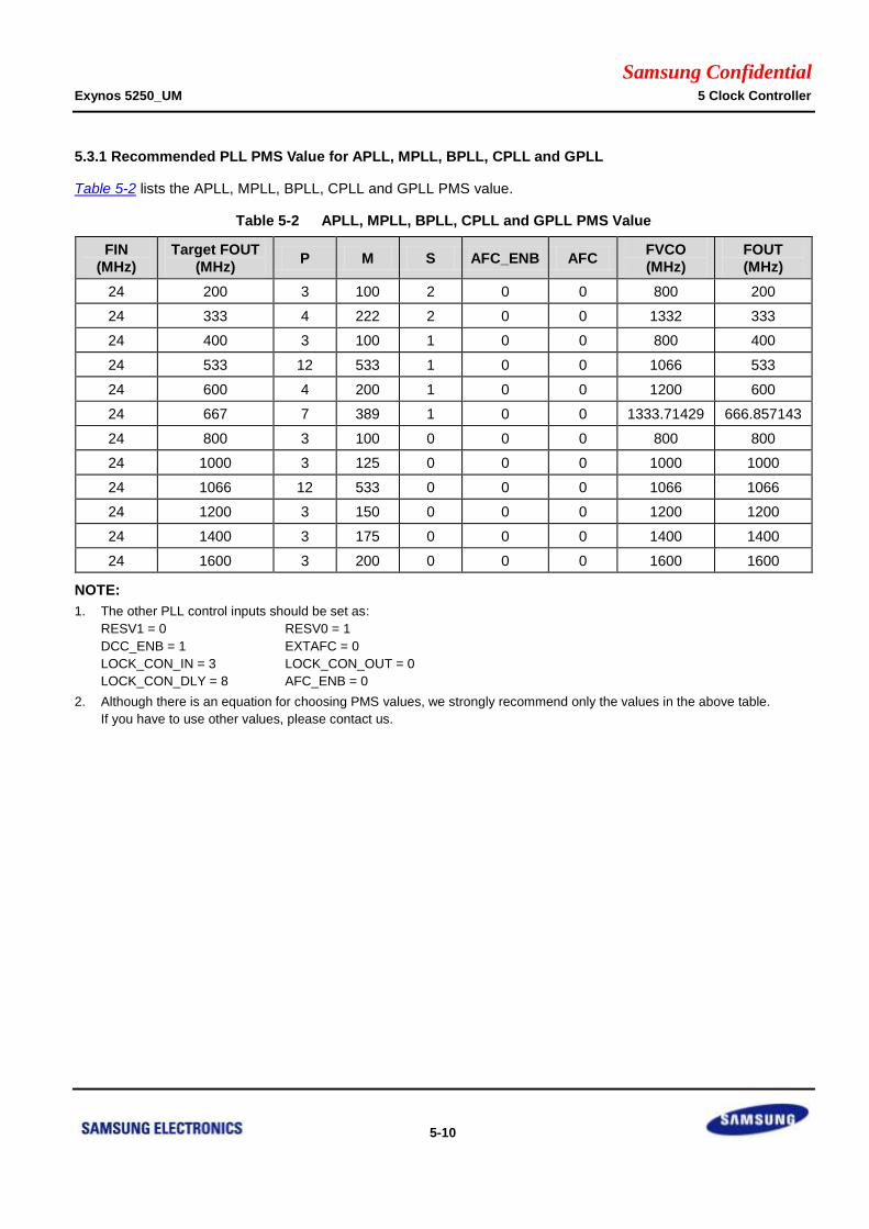
Samsung Confidential Exynos 5250_UM 5 Clock Controller
5-10
5.3.1 Recommended PLL PMS Value for APLL, MPLL, BPLL, CPLL and GPLL
Table 5-2 lists the APLL, MPLL, BPLL, CPLL and GPLL PMS value.
Table 5-2 APLL, MPLL, BPLL, CPLL and GPLL PMS Value
FIN
(MHz)
Target FOUT
(MHz) P M S AFC_ENB AFC
FVCO
(MHz)
FOUT
(MHz)
24 200 3 100 2 0 0 800 200
24 333 4 222 2 0 0 1332 333
24 400 3 100 1 0 0 800 400
24 533 12 533 1 0 0 1066 533
24 600 4 200 1 0 0 1200 600
24 667 7 389 1 0 0 1333.71429 666.857143
24 800 3 100 0 0 0 800 800
24 1000 3 125 0 0 0 1000 1000
24 1066 12 533 0 0 0 1066 1066
24 1200 3 150 0 0 0 1200 1200
24 1400 3 175 0 0 0 1400 1400
24 1600 3 200 0 0 0 1600 1600
NOTE:
1. The other PLL control inputs should be set as:
RESV1 = 0 RESV0 = 1
DCC_ENB = 1 EXTAFC = 0
LOCK_CON_IN = 3 LOCK_CON_OUT = 0
LOCK_CON_DLY = 8 AFC_ENB = 0
2. Although there is an equation for choosing PMS values, we strongly recommend only the values in the above table.
If you have to use other values, please contact us.
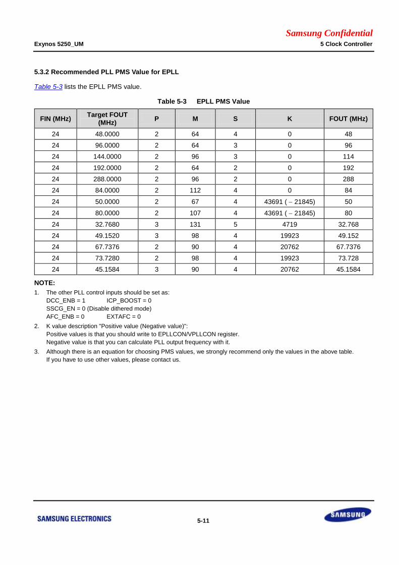
Samsung Confidential Exynos 5250_UM 5 Clock Controller
5-11
5.3.2 Recommended PLL PMS Value for EPLL
Table 5-3 lists the EPLL PMS value.
Table 5-3 EPLL PMS Value
FIN (MHz) Target FOUT
(MHz) P M S K FOUT (MHz)
24 48.0000 2 64 4 0 48
24 96.0000 2 64 3 0 96
24 144.0000 2 96 3 0 114
24 192.0000 2 64 2 0 192
24 288.0000 2 96 2 0 288
24 84.0000 2 112 4 0 84
24 50.0000 2 67 4 43691 ( 21845) 50
24 80.0000 2 107 4 43691 ( 21845) 80
24 32.7680 3 131 5 4719 32.768
24 49.1520 3 98 4 19923 49.152
24 67.7376 2 90 4 20762 67.7376
24 73.7280 2 98 4 19923 73.728
24 45.1584 3 90 4 20762 45.1584
NOTE:
1. The other PLL control inputs should be set as:
DCC_ENB = 1 ICP_BOOST = 0
SSCG_EN = 0 (Disable dithered mode)
AFC_ENB = 0 EXTAFC = 0
2. K value description "Positive value (Negative value)":
Positive values is that you should write to EPLLCON/VPLLCON register.
Negative value is that you can calculate PLL output frequency with it.
3. Although there is an equation for choosing PMS values, we strongly recommend only the values in the above table.
If you have to use other values, please contact us.
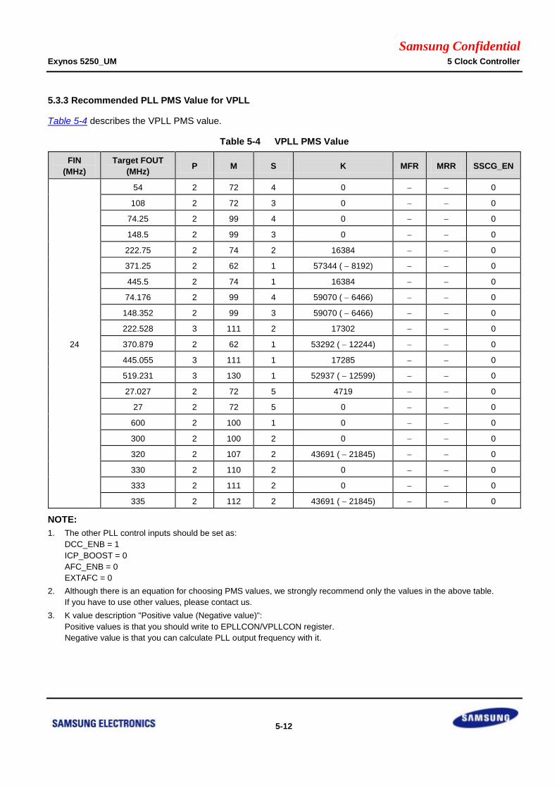
Samsung Confidential Exynos 5250_UM 5 Clock Controller
5-12
5.3.3 Recommended PLL PMS Value for VPLL
Table 5-4 describes the VPLL PMS value.
Table 5-4 VPLL PMS Value
FIN
(MHz)
Target FOUT
(MHz) P M S K MFR MRR SSCG_EN
24
54 2 72 4 0 0
108 2 72 3 0 0
74.25 2 99 4 0 0
148.5 2 99 3 0 0
222.75 2 74 2 16384 0
371.25 2 62 1 57344 ( 8192) 0
445.5 2 74 1 16384 0
74.176 2 99 4 59070 ( 6466) 0
148.352 2 99 3 59070 ( 6466) 0
222.528 3 111 2 17302 0
370.879 2 62 1 53292 ( 12244) 0
445.055 3 111 1 17285 0
519.231 3 130 1 52937 ( 12599) 0
27.027 2 72 5 4719 0
27 2 72 5 0 0
600 2 100 1 0 0
300 2 100 2 0 0
320 2 107 2 43691 ( 21845) 0
330 2 110 2 0 0
333 2 111 2 0 0
335 2 112 2 43691 ( 21845) 0
NOTE:
1. The other PLL control inputs should be set as:
DCC_ENB = 1
ICP_BOOST = 0
AFC_ENB = 0
EXTAFC = 0
2. Although there is an equation for choosing PMS values, we strongly recommend only the values in the above table.
If you have to use other values, please contact us.
3. K value description "Positive value (Negative value)":
Positive values is that you should write to EPLLCON/VPLLCON register.
Negative value is that you can calculate PLL output frequency with it.

Samsung Confidential Exynos 5250_UM 5 Clock Controller
5-13
5.4 Clock Generation
Figure 5-2 through Figure 5-5 illustrate block diagram of the clock generation logic. An external crystal clock is
connected to the oscillation amplifier. The PLL converts low input frequency to high-frequency clock that Exynos
5250 requires. The clock generator block also includes a built-in logic to stabilize the clock frequency after each
system reset, because clock takes time for stabilizing.
Figure 5-2 through Figure 5-5 also illustrates two types of clock mux. Clock mux in grey color represents glitch-
free clock mux, which is free of glitches while clock selection is changed. Clock mux in white color represents non-
glitch-free clock mux, which can suffer from glitches when changing clock sources. Care must be taken in using
each clock mux. For glitch-free mux, ensure to run all clock sources when clock selection is changed from one
mux to other mux. If the clock sources are not run, clock changing process is not finished. It might result in
unknown clock states.
For non-glitch-free clock mux, there is a possibility to have a glitch when clock selection is changed. To prevent
glitch signals, it is recommended to disable output of a non-glitch-free mux before trying to change clock sources.
After clock changing is completed, you can re-enable output of the non-glitch-free clock mux so that no glitches
will result from clock changes. Clock source mask control registers with prefix "CLK_SRC_MASK" handle
masking output of non-glitch free muxes.
Clock dividers illustrated in Figure 5-2 through Figure 5-5 indicate possible dividing value in parentheses. During
run-time, clock divider registers can change these dividing values. Some clock dividers may have only one
dividing value and user is not allowed to change the dividing value. For such dividers, that is denoted as "/2", there
is no corresponding field in clock divider registers.

Samsung Confidential Exynos 5250_UM 5 Clock Controller
5-14
Figure 5-2 and Figure 5-3 illustrate the Exynos 5250 clock generation circuit. (CPU, BUS, DRAM Clocks)
CMU_CDREX
CMU_COREMUXMPLL
MOUTMPLL
0
1
DIVRSVD3_CORE
(1~16)
MUXPWI
MOUTPWI
XXTI
XusbXTI
SCLK_HDMI27M
SCLK_DPTXPHY
SCLK_UHOSTPHYSCLK_HDMIPHY
SCLKMPLL
SCLKEPLL
SCLKVPLL
SCLKMPLL
FOUTMPLL
DIVRSVD1_CORE
(1~128)
DIVRSVD2_CORE
(1~128)
DIVCORED
(1~8)
DIVCOREP
(1~8)
ACLK_COREP
ACLK_CORED
CMU_CPU
APLL
(PLL3500)
0
1 DIVARM
(1~8) /1
0
1
XXTI
MUXAPLL
MUXCPU
MOUTCPU
FINPLL
MOUTAPLL
DIVATB
(1~8) /5
Clock stop request
When EAGLE(A15)
reset/isolation
DIVCOPY
(1~8) /8
SCLK_HPMDIVHPM
(1~8) /8DOUTCOPY
MOUTAPLL
FOUTAPLL
Voltage domain
crossing
Paired inverters are
added before/after
the line
0
1
0
1
glitch-free
mux
normal
mux
synchronous
clocks
ARM_CLK
PCLK_DBGDIVPCLK_DBG
(1~8) /2
MOUTAPLL
SCLKMPLL
DIVCPUD
(1~8) /2
ACLK_CPUD
0
1
DIVPERIPH
(1~8) /8PERIPHCLK
HCLK_CSSYS
CTMCLK
TRACECLK
ATCLKEN
DIVACP
(1~8) /8
OSCCLK
MUXHPM
MOUTHPM
DIVAPLL
(1~8) /2SCLK_APLL
PCLKEN_DBG
ATCLKE4D : PCLKDBG
CSSYS : ATCLK
E4D : PCLKENDBG → source clock = E4D : PCLKDBG
E4D : CLK
E4D : PERIPHCLKEN → source clock = E4D : CLK
CSSYS : PCLKDBG
SECJTAG : PCLK
ASYNCAXIS_EAGLE_CBX : ACLK
DIVARM2
(1~8) /1
OSCCLK RCLK_CDREX
RCLK_DREX2
BPLL
(PLL3500)DIV/2
(fixed)0
1
MUXBPLL_FOUT
MOUT_BPLL_FOUT
0
1
MUXBPLL
SCLKBPLL
MPLL
(PLL3500)DIV/2
(fixed)0
1
MUXMPLL_FOUT
MOUT_MPLL_FOUT
0
1
1600
800
DIVMCLK_CDREX
(1~8) (3)
DIVPCLK_CDREX
(1~8) (2)
PCLK_CDREX
MUXMCLK_CDREX
266 133
0
1
DIVMCLK_CDREX2
(1~8) (1)
DIVMCLK_DPHY
(1~8) (1)
MCLK_DPHYMCLK_DPHY0
MCLK_DPHY1
800
MUXMCLK_DPHY
MOUT_BPLL
MOUT_MCLK_CDREX
MOUT_MCLK_DPHY
DIVACLK_CDREX
(1~8) (2)
DIVACLK_SFRTZA
SCP
(1~8) (2)
ACLK_SFRTZASCP
200
400
800 MCLK_CDREX
ACLK_CDREX
MCLK_DREX2
synchronous
clocks
SCLKMPLL_LFT
MPLLFOUT_RGT
MPLLFOUT_RGT
800
800
CMU_ACP
PCLK_ACPDIVPCLK_ACP
(1~8) (2)
ACLK_ACP
synchronous
clocks
DIVACLK_ACP
(1~8) (3)
SCLKMPLL_LFT
DIVACLK_SYSLFT
(1~8) (2)
DIVPCLK_SYSLFT
(1~8) (2)
PCLK_SYSLFT
ACLK_SYSLFT
synchronous
clocks
DIVEFCLK_SYSLFT
(1~16) (4)
EFCLK_SYSLFT
266
133
400
200
200
DIVC2C_CLK_400
(1~8)
DIVACLK_C2C_200
(1~8)
ACLK_C2C
C2C_CLK
DIVACLK_R1BX
(1~8)
ACLK_R1BX
800
800 400
200
400
266
133
MPLL SFR is
in CMU_CORE
800
1000MHz
500MHz
1000MHz
500MHz
not used
not used
200MHz
100MHz
FOUTBPLL
not used
not used
not used
not used
Figure 5-2 Exynos 5250 Clock Generation Circuit (CPU, BUS, DRAM Clocks) 1
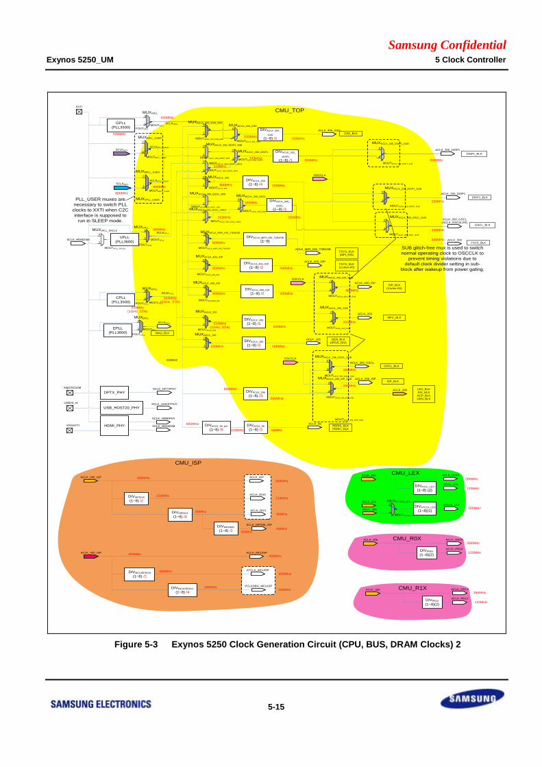
Samsung Confidential Exynos 5250_UM 5 Clock Controller
5-15
CMU_TOP
EPLL
(PLL3600)
0
1
DPTX_PHYSCLK_DPTXPHY
SCLKEPLL
MUXEPLL
MUXVPLL
FOUTEPLL
FOUTVPLL
0
1
MOUTACLK_300_DISP1_MID
MUXACLK_300_DISP1_MID
ACLK_300_DISP1DIVACLK_300_
DISP1
(1~8) /1
USB_HOST20_PHYSCLK_UHOSTPHY
DIVACLK_200
(1~8) /4
DIVACLK_266
(1~8) /3
ACLK_266
G3D_BLK
CMU_ISP
ACLK_ISP
DIVISPDIV0
(1~8) /2
ACLK_DIV0
MAU_BLK
MFC_BLK
GEN_BLK
(JPGX_DIV)
LEX_BLK
RIX_BLK
ACP_BLK
GEN_BLK
DIVACLK_66
(1~8) /2
ACLK_66PERIS_BLK
PERIC_BLK
CPLL
(PLL3500)
0
1
SCLKMPLL
0
1
MOUTACLK_333
MUXACLK_333
DIVACLK_333
(1~8) /1
DIVACLK_166
(1~8) /2
ACLK_166
FOUTCPLL
MUXCPLL
ACLK_266_ISP
200MHz
DIVISPDIV1
(1~8) /4
DIVMPWMIV
(1~8) /1
ACLK_DIV1
SCLK_MPWM_ISP
0
1
MUXACLK_166
0
1
MUXACLK_200
MOUTACLK_200
SCLKBPLL
DIVACLK_400_IOP
(1~8) /2
ACLK_400_IOPFSYS_BLK
(Cortex-A5)
0
1
MOUTACLK_400_IOP
DIVACLK_66_pre
(1~8) /6
DIVACLK_400_ISP
(1~8) /2
ISP_BLK
(Cortex-A5)0
1
MUXACLK_400_ISP
MOUTACLK400_ISP
DIVACLK_MIPI_HSI_TXBASE
(1~8)
ACLK_MIPI_HSI_TXBASEFSYS_BLK
(MPI_HIS)
0
1
MUXACLK_MIPI_HSI_TXBASE
MOUTACLK_MIPI_HSI_TXBASE
MUXACLK_400_IOP
0
1
MUXBPLL_USER
MOUTBPLL_USER
0
1
MUXMPLL_USER
MOUTMPLL_USER
PLL_USER muxes are
necessary to switch PLL
clocks to XXTI when C2C
interface is supposed to
run in SLEEP mode.
OSCCLK
DISP1_BLK
FSYS_BLK
ACLK_200_DISP10
1
MOUTACLK_200_DISP1_SUB
MUXACLK_200_DISP1_SUB
ACLK_200
ACLK_400_ISP0
1
MOUTACLK_400_ISP_SUB
MUXACLK_400_ISP_SUBOSCCLK
0
1
MUXACLK_333_SUB
MOUTACLK_333_SUB
ACLK_333
ACLK_266_GSCL0
1
MOUTACLK_266_GSCL_SUB
MUXACLK_266_GSCL_SUBOSCCLK
MOUTACLK_266_GPS_SUB
SUB glitch-free mux is used to switch
normal operating clock to OSCCLK to
prevent timing violations due to
default clock divider setting in sub-
block after wakeup from power gating.
GSCL_BLK
ISP_BLKACLK_266_ISP
0
1
MOUTACLK_266_ISP_SUB
MUXACLK_266_ISP_SUB
ACLK_MCUISP
DIVMCUISPDIV0
(1~8) /2
ATCLK_MCUISP
ACLK_400_ISP
DIVMCUISPDIV1
(1~8) /4
PCLKDBG_MCUISP
0
1DIVACLK_400_
G3D
(1~8) /1
ACLK_400_G3D
MUXACLK_400_G3D_MID
MOUTACLK_400_G3D_MID
0
1
MUXACLK_300_DISP1_SUB
0
1
MUXVPLL_USER
0
1
MOUTACLK_300_GSCL_SUB
MUXACLK_300_GSCL_SUB
DIVACLK_300_
GSCL
(1~8) /1
0
1
MUXACLK_300_GSCL_MID
MOUTACLK_300_GSCL_MID
GSCL_BLK
MUXACLK_300_DISP1
MOUTACLK_300_DISP1
ACLK_300_GSCL
(SCLK_GSCALER)
0
1
MUXACLK_300_GSCL
MOUTACLK_300_GSCL
MOUTACLK_300_DISP1_SUB
DISP1_BLK
USB20_XI
XdpOSC24M
0
1
GPLL
(PLL3500)
0
1
FOUTGPLL
MUXGPLL
MOUTACLK_400_G3D
MUXACLK_400_G3D
CMU_R0X
ACLK_PR0XDIVPR0X
(1~8)(2)
ACLK_DR0XACLK_266
CMU_R1X
ACLK_PR1XDIVPR1X
(1~8)(2)
ACLK_DR1XACLK_266
CMU_LEX
PCLK_LEXDIVPCLK_LEX
(1~8) (2)
ACLK_DLEXACLK_266
ATCLK_LEX
ACLK_200
DIVATCLK_LEX
(1~8)(1)
266MHz266MHz
133MHz
66MHz
66MHz
133MHz
66MHz
66MHz
400MHz400MHz
200MHz
100MHz
200MHz
100MHz
533MHz
533MHz
533MHz
800MHz
800MHz
300MHz
533MHz
333MHz333MHz
200MHz800MHz
333MHz
333MHz
800MHz
800MHz
800MHz
333MHz
(1GHz, STA)
333MHz
(1GHz, STA)
333MHz
(1GHz, STA)
333MHz 166MHz
333MHz
800MHz
800MHz
133MHz 66MHz
266MHz
400MHz
400MHz
200MHz
333MHz
200MHz
333MHz
400MHz
333MHz
266MHz
266MHz
0
1ACLK_266
266MHz
133MHz
266MHz
133MHz
200MHz
266MHz
133MHz
0
1 MOUTACLK_300_DISP1_MID1
MUXACLK_300_DISP1_MID1
0
1
MUXACLK_300_GSCL_MID1
MOUTACLK_300_GSCL_MID1
333MHz
333MHz
VPLL
(PLL3600)
0
1
0
1SCLK_HDMI24M
MUXVPLL_SRCLK
XXTI
SCLKBPLL_USER
SCLKMPLL_USER
MUXATCLK_LEX
MOUTATCLK_LEX
MOUTVPLL
MOUTGPLL
MOUTCPLL
MOUTEPLL
MOUTVPLL_SRCLK
SCLKVPLL
SCLKCPLL
SCLKGPLL
HDMI_PHY
SCLK_HDMIPHY
SCLK_HDMI24MXhdmiXTI
Figure 5-3 Exynos 5250 Clock Generation Circuit (CPU, BUS, DRAM Clocks) 2
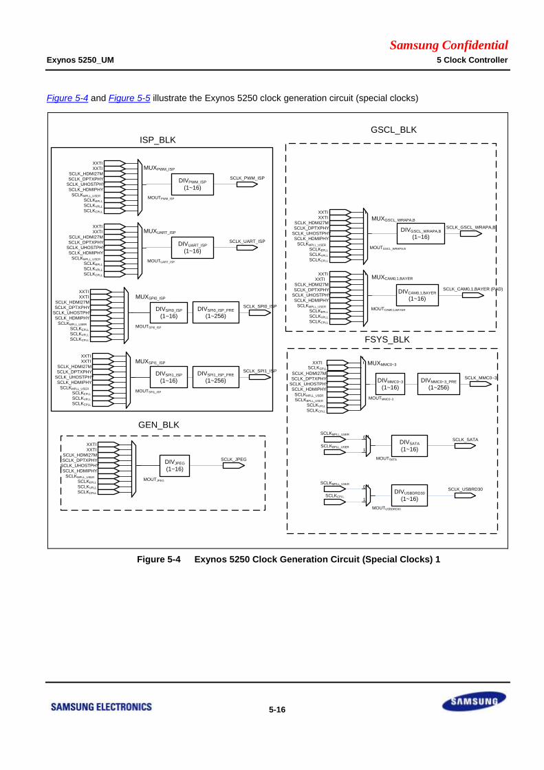
Samsung Confidential Exynos 5250_UM 5 Clock Controller
5-16
Figure 5-4 and Figure 5-5 illustrate the Exynos 5250 clock generation circuit (special clocks)
MUXMMC0~3
MOUTMMC0~3
FSYS_BLK
SCLK_MMC0~3DIVMMC0~3
(1~16)
DIVMMC0~3_PRE
(1~256)
XXTI
SCLK_HDMI27M
SCLK_DPTXPHY
SCLK_UHOSTPHY
SCLK_HDMIPHY
SCLKVPLL
SCLKCPLL
GEN_BLK
SCLKMPLL_USER
SCLKCPLL
0
1
DIVUSBDRD30
(1~16)
SCLK_USBRD30
MOUTUSBDRD30
ISP_BLK
DIVPWM_ISP
(1~16)
SCLK_PWM_ISP
MUXPWM_ISP
MOUTPWM_ISP
DIVUART_ISP
(1~16)
SCLK_UART_ISP
MUXUART_ISP
MOUTUART_ISP
DIVSPI1_ISP
(1~16)
SCLK_SPI1_ISP
MUXSPI1_ISP
MOUTSPI1_ISP
DIVSPI1_ISP_PRE
(1~256)
DIVSPI0_ISP
(1~16)
SCLK_SPI0_ISP
MUXSPI0_ISP
MOUTSPI0_ISP
DIVSPI0_ISP_PRE
(1~256)
SCLKMPLL_USER
DIVCAM0,1,BAYER
(1~16)
SCLK_CAM0,1,BAYER (PAD)
MUXCAM0,1,BAYER
MOUTCAM0,1,BAYER
DIVGSCL_WRAPA,B
(1~16)
SCLK_GSCL_WRAPA,B
MUXGSCL_WRAPA,B
MOUTGSCL_WRAPA,B
GSCL_BLK
XXTI
XXTI
SCLK_HDMI27M
SCLK_DPTXPHY
SCLK_UHOSTPHY
SCLK_HDMIPHY
SCLKEPLL
SCLKVPLL
SCLKCPLL
SCLKMPLL_USER
SCLKMPLL_USER
SCLKBPLL_USER
0
1
DIVSATA
(1~16)
SCLK_SATA
MOUTSATA
SCLKGPLL
XXTI
SCLK_HDMI27M
SCLK_DPTXPHY
SCLK_UHOSTPHY
SCLK_HDMIPHY
SCLKEPLL
SCLKVPLL
SCLKCPLL
SCLKMPLL_USER
XXTI
XXTI
SCLK_HDMI27M
SCLK_DPTXPHY
SCLK_UHOSTPHY
SCLK_HDMIPHY
SCLKEPLL
SCLKVPLL
SCLKCPLL
SCLKMPLL_USER
XXTI
XXTI
SCLK_HDMI27M
SCLK_DPTXPHY
SCLK_UHOSTPHY
SCLK_HDMIPHY
SCLKEPLL
SCLKVPLL
SCLKCPLL
SCLKMPLL_USER
XXTI
XXTI
SCLK_HDMI27M
SCLK_DPTXPHY
SCLK_UHOSTPHY
SCLK_HDMIPHY
SCLKEPLL
SCLKVPLL
SCLKCPLL
SCLKMPLL_USER
XXTI
XXTI
SCLK_HDMI27M
SCLK_DPTXPHY
SCLK_UHOSTPHY
SCLK_HDMIPHY
SCLKEPLL
SCLKVPLL
SCLKCPLL
SCLKMPLL_USER
XXTI
DIVJPEG
(1~16)
SCLK_JPEG
MOUTJPEG
XXTI
SCLK_HDMI27M
SCLK_DPTXPHY
SCLK_UHOSTPHY
SCLK_HDMIPHY
SCLKEPLL
SCLKVPLL
SCLKCPLL
SCLKMPLL_USER
XXTI
SCLKBPLL_USER
Figure 5-4 Exynos 5250 Clock Generation Circuit (Special Clocks) 1

Samsung Confidential Exynos 5250_UM 5 Clock Controller
5-17
DIVAUDIO0
(1~16)
SCLK_AUDIO0
MUXAUDIO0
DIVAUDIO1
(1~16)
SCLK_AUDIO1
MUXAUDIO1
DIVAUDIO2
(1~16)
SCLK_AUDIO2
MUXAUDIO2
MOUTAUDIO0
MOUTAUDIO1
MOUTAUDIO2
AUDIO_BLK
SCLK_HDMIDIVHDMI_PIXEL
(1~16)
SCLKVPLL0
1SCLK_HDMIPHY
MUXHDMI
SCLK_PIXEL
DIVPCM0~2
(1~256)
SCLK_PCM0~2SCLK_AUDIO0~2
SCLK_AUDIO0
SCLK_AUDIO1
SCLK_AUDIO2
SPDIF_EXTCLK
SCLK_SPDIFMUXSPDIF
DIVI2S1~2
(1~64)
SCLK_I2S1~2SCLK_AUDIO1~2
DISP1_BLK
DIVFIMD1
(1~16)
SCLK_FIMD1
MUXFIMD1
MOUTFIMCD1
DIVMIPI1
(1~16)
SCLK_MIPI1
MUXMIPI1
MOUTMIPI1
DIVMIPI1_PRE
(1~16)
SCLK_MIPIDPHY1
DIVEXT_MST_VID
(1~16)
SCLK_DP1_EXT_MST_VID
MUXDP1_EXT_MST_VID
MOUTDP1_EXT_MST_VID
DIVSPI0~2
(1~16)
SCLK_SPI0~2
DIVUART0~3
(1~16)
SCLK_UART0~3
MUXSPI0~2
MUXUART0~3
MOUTUART0~3
MOUTSPI0~2
PERI_BLK
DIVSPI0~2_PRE
(1~256)
XXTI
SCLK_HDMI27M
SCLK_DPTXPHY
SCLK_UHOSTPHY
SCLK_HDMIPHY
SCLKEPLL
SCLKVPLL
SCLKCPLL
SCLKMPLL_USER
XXTI
XXTI
SCLK_HDMI27M
SCLK_DPTXPHY
SCLK_UHOSTPHY
SCLK_HDMIPHY
SCLKEPLL
SCLKVPLL
SCLKCPLL
SCLKMPLL_USER
XXTI
XXTI
SCLK_HDMI27M
SCLK_DPTXPHY
SCLK_UHOSTPHY
SCLK_HDMIPHY
SCLKEPLL
SCLKVPLL
SCLKCPLL
SCLKMPLL_USER
XXTI
XXTI
SCLK_HDMI27M
SCLK_DPTXPHY
SCLK_UHOSTPHY
SCLK_HDMIPHY
SCLKEPLL
SCLKVPLL
SCLKCPLL
SCLKMPLL_USER
XXTI
XXTI
SCLK_HDMI27M
SCLK_DPTXPHY
SCLK_UHOSTPHY
SCLK_HDMIPHY
SCLKEPLL
SCLKVPLL
SCLKCPLL
SCLKMPLL_USER
XXTI
AUDIOCDCLK0
XXTI
SCLK_HDMI27M
SCLK_DPTXPHY
SCLK_UHOSTPHY
SCLKEPLL
SCLKVPLL
SCLKCPLL
SCLKMPLL_USER
XXTI
AUDIOCDCLK0
XXTI
SCLK_HDMI27M
SCLK_DPTXPHY
SCLK_UHOSTPHY
SCLKEPLL
SCLKVPLL
SCLKCPLL
SCLKMPLL_USER
XXTI
AUDIOCDCLK0
XXTI
SCLK_HDMI27M
SCLK_DPTXPHY
SCLK_UHOSTPHY
SCLKEPLL
SCLKVPLL
SCLKCPLL
SCLKMPLL_USER
XXTI
Figure 5-5 Exynos 5250 Clock Generation Circuit (Special Clocks) 2
Caution: In Figure 5-2 and Figure 5-5, muxes with grey color are glitch-free. For glitch-free clock muxes,
ensure that all clock sources are running when clock selection is changed.
For clock dividers, ensure that input clock is running when divider value is changed
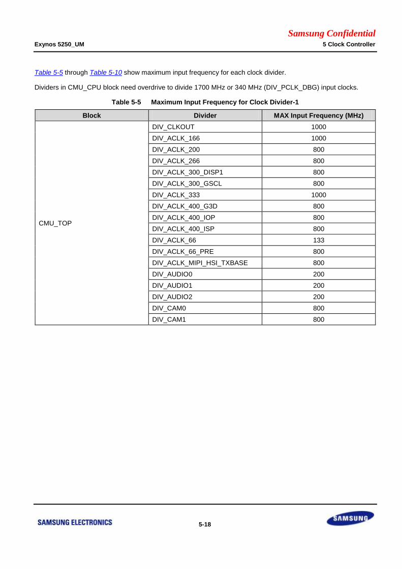
Samsung Confidential Exynos 5250_UM 5 Clock Controller
5-18
Table 5-5 through Table 5-10 show maximum input frequency for each clock divider.
Dividers in CMU_CPU block need overdrive to divide 1700 MHz or 340 MHz (DIV_PCLK_DBG) input clocks.
Table 5-5 Maximum Input Frequency for Clock Divider-1
Block Divider MAX Input Frequency (MHz)
CMU_TOP
DIV_CLKOUT 1000
DIV_ACLK_166 1000
DIV_ACLK_200 800
DIV_ACLK_266 800
DIV_ACLK_300_DISP1 800
DIV_ACLK_300_GSCL 800
DIV_ACLK_333 1000
DIV_ACLK_400_G3D 800
DIV_ACLK_400_IOP 800
DIV_ACLK_400_ISP 800
DIV_ACLK_66 133
DIV_ACLK_66_PRE 800
DIV_ACLK_MIPI_HSI_TXBASE 800
DIV_AUDIO0 200
DIV_AUDIO1 200
DIV_AUDIO2 200
DIV_CAM0 800
DIV_CAM1 800

Samsung Confidential Exynos 5250_UM 5 Clock Controller
5-19
Table 5-6 Maximum Input Frequency for Clock Divider-2
Block Divider MAX Input Frequency (MHz)
CMU_TOP
DIV_CAM_BAYER 800
DIV_DP1_EXT_MST_VID 900
DIV_FIMD1 900
DIV_GSCL_WRAP_A 800
DIV_GSCL_WRAP_B 800
DIV_HDMI_PIXEL 900
DIV_I2S1 100
DIV_I2S2 100
DIV_JPEG 333
DIV_MIPI1 920
DIV_MIPI1_PRE 115
DIV_MMC0 800
DIV_MMC0_PRE 800
DIV_MMC1 800
DIV_MMC1_PRE 800
DIV_MMC2 800
DIV_MMC2_PRE 800
DIV_MMC3 800
DIV_MMC3_PRE 800
DIV_PCM0 100
DIV_PCM1 100
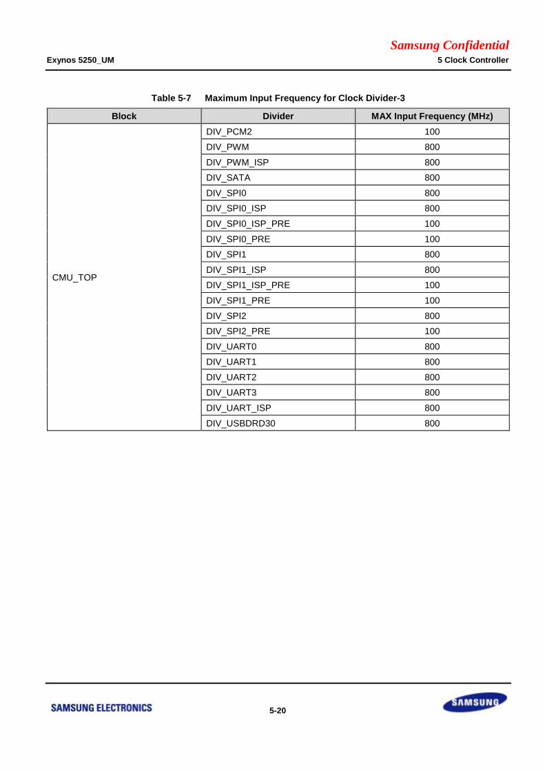
Samsung Confidential Exynos 5250_UM 5 Clock Controller
5-20
Table 5-7 Maximum Input Frequency for Clock Divider-3
Block Divider MAX Input Frequency (MHz)
CMU_TOP
DIV_PCM2 100
DIV_PWM 800
DIV_PWM_ISP 800
DIV_SATA 800
DIV_SPI0 800
DIV_SPI0_ISP 800
DIV_SPI0_ISP_PRE 100
DIV_SPI0_PRE 100
DIV_SPI1 800
DIV_SPI1_ISP 800
DIV_SPI1_ISP_PRE 100
DIV_SPI1_PRE 100
DIV_SPI2 800
DIV_SPI2_PRE 100
DIV_UART0 800
DIV_UART1 800
DIV_UART2 800
DIV_UART3 800
DIV_UART_ISP 800
DIV_USBDRD30 800

Samsung Confidential Exynos 5250_UM 5 Clock Controller
5-21
Table 5-8 Maximum Input Frequency for Clock Divider-4
Block Divider MAX Input Frequency (MHz)
CMU_CPU
DIV_CLKOUT 1265
DIV_ACP (not used) 1700
DIV_APLL 1700
DIV_ARM 1700
DIV_ARM2 1700
DIV_ATB 1700
DIV_COPY 800
DIV_CPUD 1700
DIV_HPM 800
DIV_PCLK_DBG 340
DIV_PERIPH (not used) 1700
CMU_ISP
DIV_CLKOUT 550
DIV_ISPDIV0 266
DIV_ISPDIV1 266
DIV_MPWMDIV 66
DIV_MCUISPDIV0 400
DIV_MCUISPDIV1 400
CMU_LEX
DIV_CLKOUT 266
DIV_ATLEX 266
DIV_PLEX 266
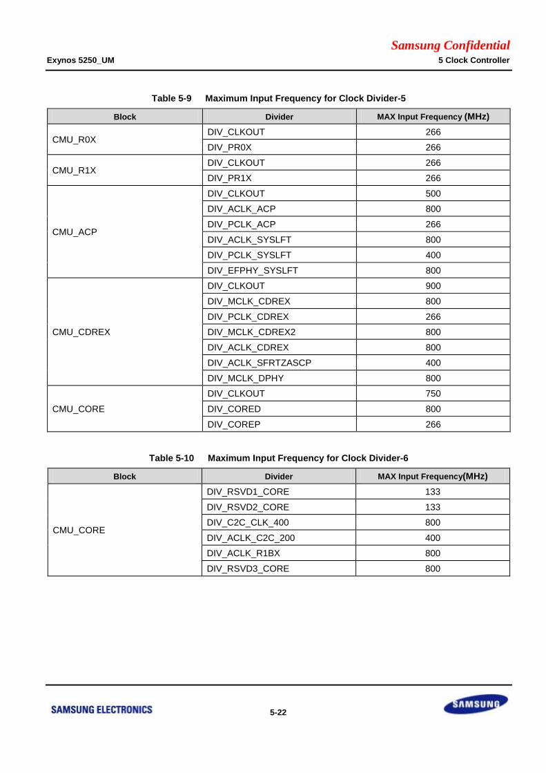
Samsung Confidential Exynos 5250_UM 5 Clock Controller
5-22
Table 5-9 Maximum Input Frequency for Clock Divider-5
Block Divider MAX Input Frequency (MHz)
CMU_R0X DIV_CLKOUT 266
DIV_PR0X 266
CMU_R1X DIV_CLKOUT 266
DIV_PR1X 266
CMU_ACP
DIV_CLKOUT 500
DIV_ACLK_ACP 800
DIV_PCLK_ACP 266
DIV_ACLK_SYSLFT 800
DIV_PCLK_SYSLFT 400
DIV_EFPHY_SYSLFT 800
CMU_CDREX
DIV_CLKOUT 900
DIV_MCLK_CDREX 800
DIV_PCLK_CDREX 266
DIV_MCLK_CDREX2 800
DIV_ACLK_CDREX 800
DIV_ACLK_SFRTZASCP 400
DIV_MCLK_DPHY 800
CMU_CORE
DIV_CLKOUT 750
DIV_CORED 800
DIV_COREP 266
Table 5-10 Maximum Input Frequency for Clock Divider-6
Block Divider MAX Input Frequency(MHz)
CMU_CORE
DIV_RSVD1_CORE 133
DIV_RSVD2_CORE 133
DIV_C2C_CLK_400 800
DIV_ACLK_C2C_200 400
DIV_ACLK_R1BX 800
DIV_RSVD3_CORE 800
Samsung Confidential Exynos 5250_UM 5 Clock Controller
5-23
5.5 Clock Configuration Procedure
You should follow these rules while changing clock configuration: You should run all inputs of a glitch-free
mux.
You should not select the output of PLL when a PLL is turned off.
Basic SFR Configuration Flows:
1. Change the system clock divider values as:
CLK_DIV_CPU0[31:0] = target value 0;
CLK_DIV_CORE0[31:0] = target value 1;
CLK_DIV_CDREX[31:0] = target value 2;
CLK_DIV_ACP[31:0] = target value 3;
CLK_DIV_ISP[31:0] = target value 4;
CLK_DIV_TOP[31:0] = target value 5;
CLK_DIV_LEX[31:0] = target value 6;
CLK_DIV_R0X[31:0] = target value 7;
CLK_DIV_R1X[31:0] = target value 8;
2. Change the divider values for special clocks by setting CLK_DIV_XXX SFRs in CMU_TOP
CLK_DIV_XXX[31:0] = target value;
3. Change PLL PMS values
Set PMS values:
// Set PDIV, MDIV, and SDIV values
(Refer to (A, M, B, C, E, G, V) PLL_CON0 SFRs for more
information)
4. Change other PLL control values
(A, M, B, C, E, G, V) PLL_CON1[31:0] = target value;
// Set K, AFC, MRR, and MFR values if necessary
(Refer to (A, M, B, C, E, G, V) PLL_CON1 SFRs for more
information)
Samsung Confidential Exynos 5250_UM 5 Clock Controller
5-24
5. Turn on a PLL
(A, M, B, C, E, G, V) PLL_CON0[31] = 1;
// Turn on a PLL (Refer to (A, M, B, C, E, G, V) PLL_CON0 SFRs
for more information)
wait_lock_time;
// Wait until the PLL is locked
MUX_(A, M, B, C, E, G, V) PLL_SEL = 1;
// After PLL output clock is stabilized, select the PLL output
clock instead of input reference clock. (Refer to CLK_SRC_CPU
SFR for APLL, CLK_SRC_CORE1 SFR for MPLL,
CLK_SRC_CDREX for BPLL, and CLK_SRC_TOP2 for CPLL,
GPLL, EPLL and VPLL for more information) When a PLL is
turned on,do not turn it off.
Samsung Confidential Exynos 5250_UM 5 Clock Controller
5-25
5.5.1 Clock Gating
Exynos 5250 can disable the clock operation of each IP if it is not required. Disabling the clock operation reduces
the dynamic power.
There are two types of clock gating control registers to Disable/Enable clock operation:
Clock gating control register for function block
Clock gating control register for IP
These two registers are AND operated together to generate a final clock gating enable signal. As a result, if either
of the two register field is turned OFF, the resulting clock is stopped. For example, to stop clocks that are provided
to MIXER module, you may set CLK_MIXER field in CLK_GATE_IP_DISP1 register to 0 or CLK_DISP1 field in
CLK_GATE_BLOCK register to 0.
NOTE: For latter case, all clocks in DISP1 block including MIXER clocks are turned off.
Caution: It should be guaranteed that S/W does not access IPs whose clock is gated. It may cause system
failure.
5.5.2 Clock Diving
Whenever clock divider control register is changed, it is recommended that you verify clock divider status registers
before using the new clock output. This guarantees the corresponding divider finishes changing to a new dividing
value before its output is used by other modules.
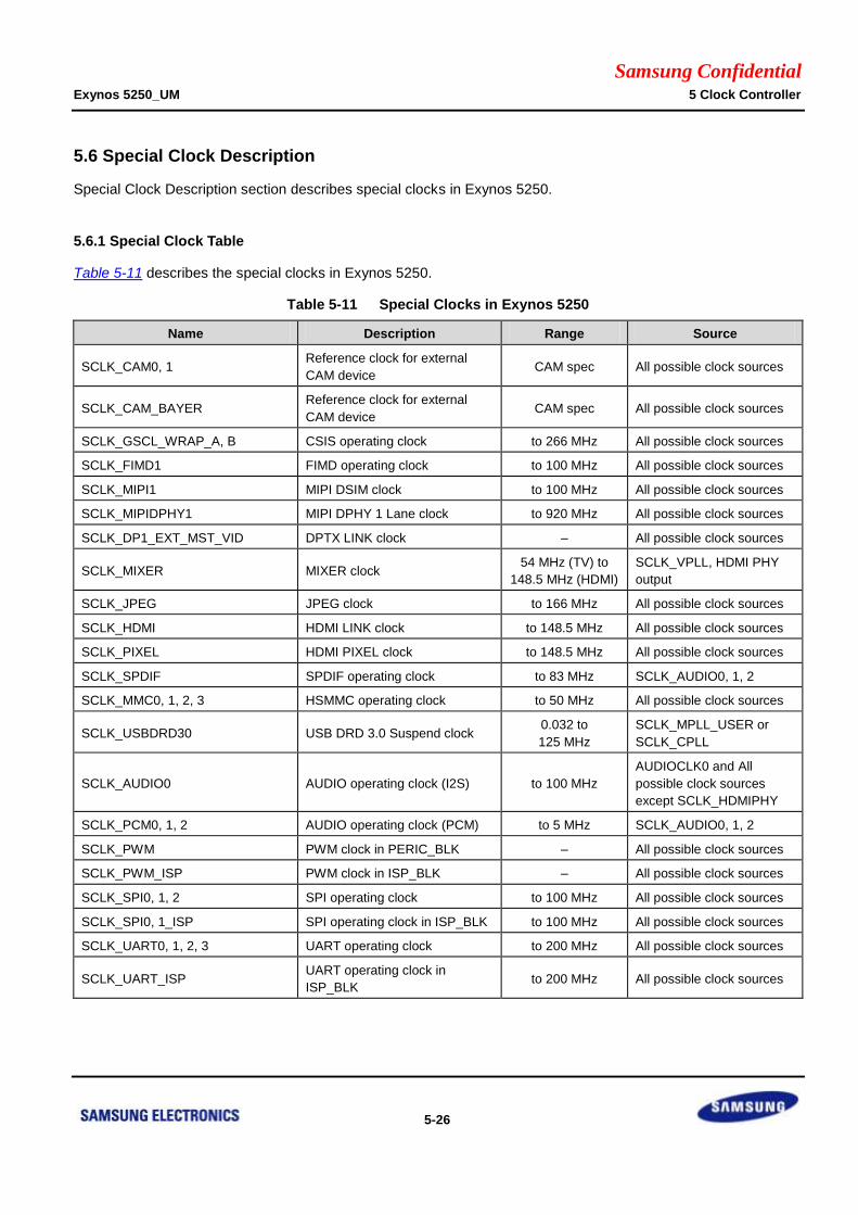
Samsung Confidential Exynos 5250_UM 5 Clock Controller
5-26
5.6 Special Clock Description
Special Clock Description section describes special clocks in Exynos 5250.
5.6.1 Special Clock Table
Table 5-11 describes the special clocks in Exynos 5250.
Table 5-11 Special Clocks in Exynos 5250
Name Description Range Source
SCLK_CAM0, 1 Reference clock for external
CAM device CAM spec All possible clock sources
SCLK_CAM_BAYER Reference clock for external
CAM device CAM spec All possible clock sources
SCLK_GSCL_WRAP_A, B CSIS operating clock to 266 MHz All possible clock sources
SCLK_FIMD1 FIMD operating clock to 100 MHz All possible clock sources
SCLK_MIPI1 MIPI DSIM clock to 100 MHz All possible clock sources
SCLK_MIPIDPHY1 MIPI DPHY 1 Lane clock to 920 MHz All possible clock sources
SCLK_DP1_EXT_MST_VID DPTX LINK clock – All possible clock sources
SCLK_MIXER MIXER clock 54 MHz (TV) to
148.5 MHz (HDMI)
SCLK_VPLL, HDMI PHY
output
SCLK_JPEG JPEG clock to 166 MHz All possible clock sources
SCLK_HDMI HDMI LINK clock to 148.5 MHz All possible clock sources
SCLK_PIXEL HDMI PIXEL clock to 148.5 MHz All possible clock sources
SCLK_SPDIF SPDIF operating clock to 83 MHz SCLK_AUDIO0, 1, 2
SCLK_MMC0, 1, 2, 3 HSMMC operating clock to 50 MHz All possible clock sources
SCLK_USBDRD30 USB DRD 3.0 Suspend clock 0.032 to
125 MHz
SCLK_MPLL_USER or
SCLK_CPLL
SCLK_AUDIO0 AUDIO operating clock (I2S) to 100 MHz
AUDIOCLK0 and All
possible clock sources
except SCLK_HDMIPHY
SCLK_PCM0, 1, 2 AUDIO operating clock (PCM) to 5 MHz SCLK_AUDIO0, 1, 2
SCLK_PWM PWM clock in PERIC_BLK – All possible clock sources
SCLK_PWM_ISP PWM clock in ISP_BLK – All possible clock sources
SCLK_SPI0, 1, 2 SPI operating clock to 100 MHz All possible clock sources
SCLK_SPI0, 1_ISP SPI operating clock in ISP_BLK to 100 MHz All possible clock sources
SCLK_UART0, 1, 2, 3 UART operating clock to 200 MHz All possible clock sources
SCLK_UART_ISP UART operating clock in
ISP_BLK to 200 MHz All possible clock sources
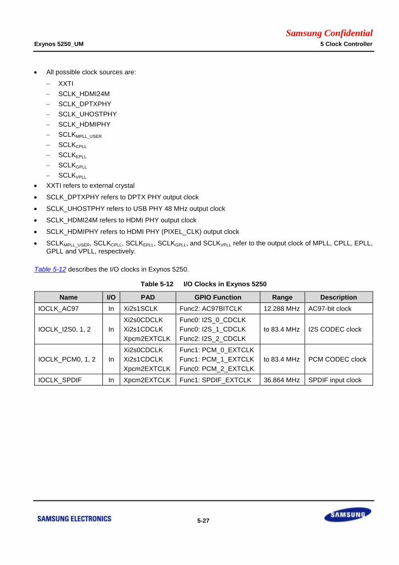
Samsung Confidential Exynos 5250_UM 5 Clock Controller
5-27
All possible clock sources are:
XXTI
SCLK_HDMI24M
SCLK_DPTXPHY
SCLK_UHOSTPHY
SCLK_HDMIPHY
SCLKMPLL_USER
SCLKCPLL
SCLKEPLL
SCLKGPLL
SCLKVPLL
XXTI refers to external crystal
SCLK_DPTXPHY refers to DPTX PHY output clock
SCLK_UHOSTPHY refers to USB PHY 48 MHz output clock
SCLK_HDMI24M refers to HDMI PHY output clock
SCLK_HDMIPHY refers to HDMI PHY (PIXEL_CLK) output clock
SCLKMPLL_USER, SCLKCPLL, SCLKEPLL, SCLKGPLL, and SCLKVPLL refer to the output clock of MPLL, CPLL, EPLL,
GPLL and VPLL, respectively.
Table 5-12 describes the I/O clocks in Exynos 5250.
Table 5-12 I/O Clocks in Exynos 5250
Name I/O PAD GPIO Function Range Description
IOCLK_AC97 In Xi2s1SCLK Func2: AC97BITCLK 12.288 MHz AC97-bit clock
IOCLK_I2S0, 1, 2 In
Xi2s0CDCLK
Xi2s1CDCLK
Xpcm2EXTCLK
Func0: I2S_0_CDCLK
Func0: I2S_1_CDCLK
Func2: I2S_2_CDCLK
to 83.4 MHz I2S CODEC clock
IOCLK_PCM0, 1, 2 In
Xi2s0CDCLK
Xi2s1CDCLK
Xpcm2EXTCLK
Func1: PCM_0_EXTCLK
Func1: PCM_1_EXTCLK
Func0: PCM_2_EXTCLK
to 83.4 MHz PCM CODEC clock
IOCLK_SPDIF In Xpcm2EXTCLK Func1: SPDIF_EXTCLK 36.864 MHz SPDIF input clock
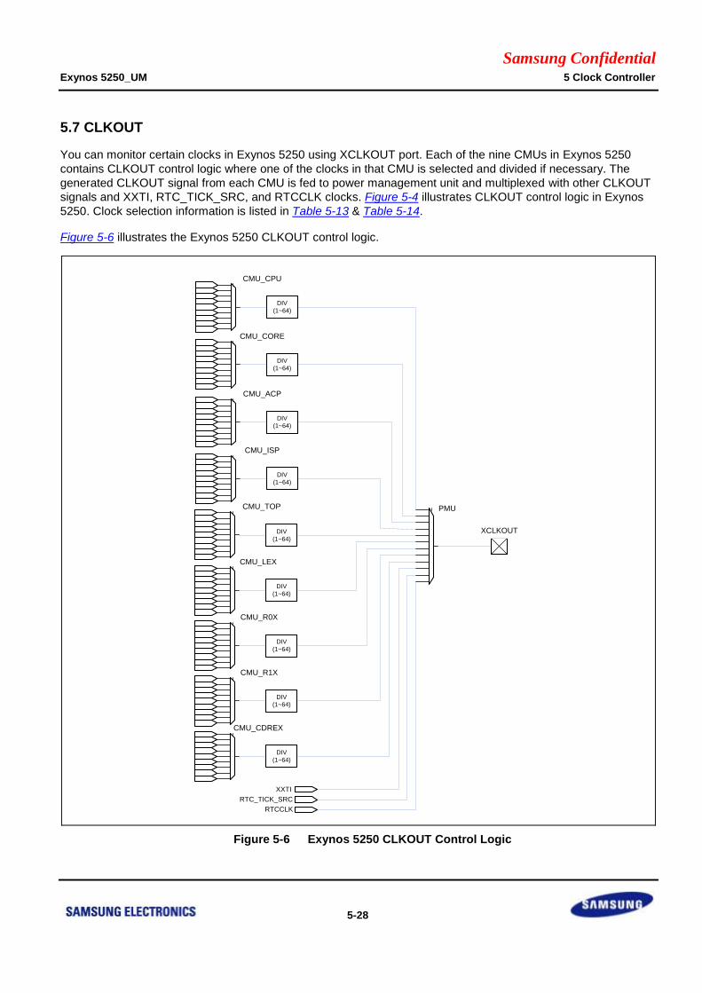
Samsung Confidential Exynos 5250_UM 5 Clock Controller
5-28
5.7 CLKOUT
You can monitor certain clocks in Exynos 5250 using XCLKOUT port. Each of the nine CMUs in Exynos 5250
contains CLKOUT control logic where one of the clocks in that CMU is selected and divided if necessary. The
generated CLKOUT signal from each CMU is fed to power management unit and multiplexed with other CLKOUT
signals and XXTI, RTC_TICK_SRC, and RTCCLK clocks. Figure 5-4 illustrates CLKOUT control logic in Exynos
5250. Clock selection information is listed in Table 5-13 & Table 5-14.
Figure 5-6 illustrates the Exynos 5250 CLKOUT control logic.
Figure 5-6 Exynos 5250 CLKOUT Control Logic
DIV
(1~64)
DIV
(1~64)
DIV
(1~64)
DIV
(1~64)
DIV
(1~64)
XXTI
RTC_TICK_SRC
RTCCLK
XCLKOUT
CMU_TOP
CMU_LEX
CMU_R0X
CMU_R1X
CMU_CDREX
PMU
DIV
(1~64)
CMU_ISP
DIV
(1~64)
CMU_ACP
DIV
(1~64)
CMU_CORE
DIV
(1~64)
CMU_CPU

Samsung Confidential Exynos 5250_UM 5 Clock Controller
5-29
Table 5-13 lists the CLKOUT input clock selection information.
Table 5-13 CLKOUT Input Clock Selection Information (Part 1)
NO CMU_CPU CMU_CORE CMU_CDREX CMU_ISP CMU_TOP PMU
0 APLL_FOUT MPLL_FOUT
_RGT MCLK_CDREX ACLK_266 EPLL_FOUT PMU_DEBUG
1 – – ACLK_CDREX ACLK_DIV0 VPLL_FOUT CMU_CDREX
2 – – PCLK_CDREX ACLK_DIV1 CPLL_FOUT CMU_CORE
3 – – RCLK_CDREX SCLK_MPWM
_ISP SCLK_HDMI24M CMU_ISP
4 ARMCLK – – – SCLK_DPTXPHY CMU_LEX
5 ACLK_CPUD ACLK_CORED – – SCLK_UHOSTPHY CMU_R0X
6 – ACLK_COREP – – SCLK_HDMIPHY CMU_R1X
7 ATCLK SCLK_RSVD3
_CORE – – AUDIOCDCLK0 CMU_TOP
8 PERIPHCLK ACLK_R1BX – – AUDIOCDCLK1 CMU_CPU
9 PCLK_DBG C2C_CLK – – AUDIOCDCLK2 CMU_ACP
10 SCLK_HPM – – – SPDIF_EXTCLK –
11 – – – – ACLK_400_G3D –
12 – – – – ACLK_333 –
13 – – – – ACLK_266 –
14 – – – – GPLL_FOUT –
15 – – – – ACLK_400_ISP –
16 – – – – ACLK_400_IOP XXTI
17 – – – – SCLK_JPEG –
18 – – – – RX_HALF_BYTE
_CLK_A
RTC_TICK
_SRC
19 – – – – RX_HALF_BYTE
_CLK_B RTCCLK
20 – – – – CAM_A_PCLK –
21 – – – – CAM_B_PCLK
22 – – – – S_RXBYTECLKHS0
_2L –
23 – – – – S_RXBYTECLKHS0
_4L –
24 – – – – ACLK_300_DISP1 –
25 – – – – ACLK_300_GSCL –
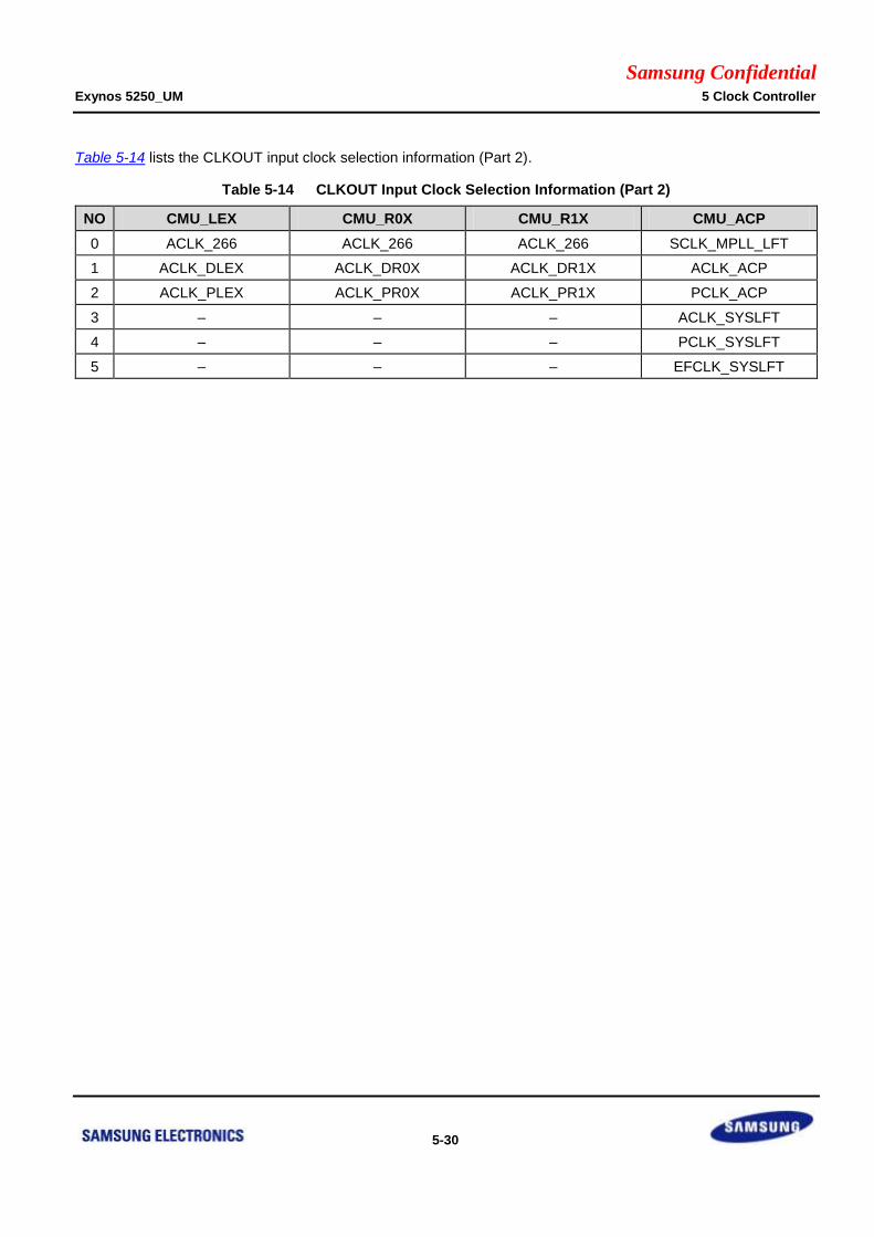
Samsung Confidential Exynos 5250_UM 5 Clock Controller
5-30
Table 5-14 lists the CLKOUT input clock selection information (Part 2).
Table 5-14 CLKOUT Input Clock Selection Information (Part 2)
NO CMU_LEX CMU_R0X CMU_R1X CMU_ACP
0 ACLK_266 ACLK_266 ACLK_266 SCLK_MPLL_LFT
1 ACLK_DLEX ACLK_DR0X ACLK_DR1X ACLK_ACP
2 ACLK_PLEX ACLK_PR0X ACLK_PR1X PCLK_ACP
3 – – – ACLK_SYSLFT
4 – – – PCLK_SYSLFT
5 – – – EFCLK_SYSLFT

Samsung Confidential Exynos 5250_UM 5 Clock Controller
5-31
5.8 I/O Description
Signal I/O Description Pad Type
XXTI Input External oscillator pad XXTI Dedicated
EPLLFILTER Input/Output Pad for EPLL loop Filter capacitor XEPLLFILTER Dedicated
VPLLFILTER Input/Output Pad for VPLL loop Filter capacitor XVPLLFILTER Dedicated
XCLKOUT Output Clock Out pad XCLKOUT Dedicated
Samsung Confidential Exynos 5250_UM 5 Clock Controller
5-32
5.9 Register Description
Clock controller controls PLLs and clock generation units. This section describes how to control these parts using
Special Functional Registers (SFRs) in the clock controller. Do not change any reserved area. Changing value of
reserved area may lead to unexpected behavior.
Figure 5-5 illustrates the address map of Exynos 5250 clock controller. There are nine CMUs in Exynos 5250 and
each CMU uses 16 KB address space for SFRs. The nine CMUs are CMU_CPU, CMU_CORE, CMU_ACP,
CMU_ISP, CMU_TOP, CMU_LEX, CMU_R0X, CMU_R1X, and CMU_CDREX. The internal structure of the
address space for each CMU is similar to all CMUs. This structure is illustrated in the right part of Figure 5-5. The
internal structure is divided into these categories:
0x000 to 0x1FF is used for PLL control: PLL lock time and control
0x200 to 0x4FF is used for mux control: Mux selection, output masking, and status
0x500 to 0x6FF is used for clock division: Divider ratio and status
0x700 to 0x8FF is reserved and user is not allowed to access the region.
0x900 to 0x9FF is used for clock gating control: Clock gating of IPs and function blocks
0xA00 to 0xAFF is used for CLKOUT: CLKOUT input clock selection and divider ratio
NOTE: For CMU_ACP, CMU_ISP, CMU_LEX and CMU_R0X/R1X, CLK_GATE_IP_XXX registers are located at 0x800.
Additionally, some CMUs use addresses beyond 0xAFF for other functions such as CPU in CMU_CPU. Refer to
register description for more information.
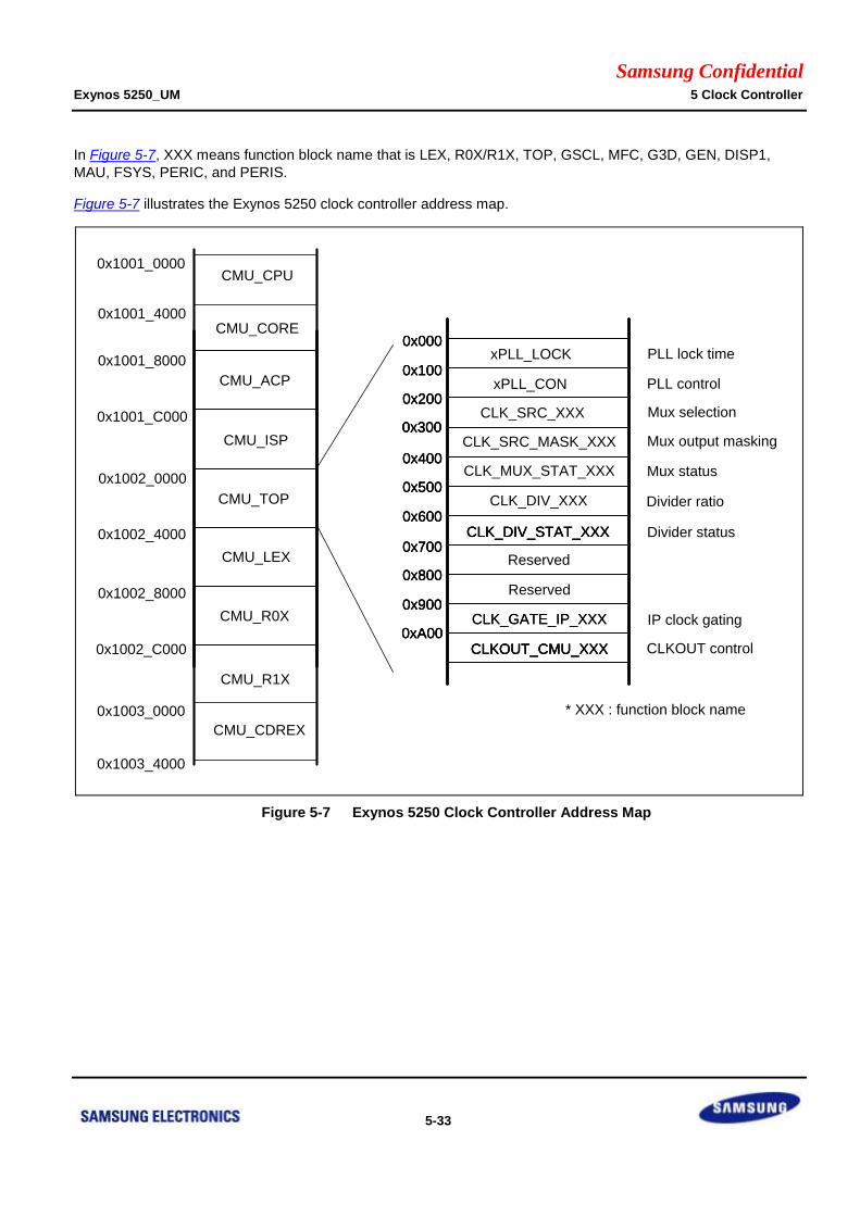
Samsung Confidential Exynos 5250_UM 5 Clock Controller
5-33
In Figure 5-7, XXX means function block name that is LEX, R0X/R1X, TOP, GSCL, MFC, G3D, GEN, DISP1,
MAU, FSYS, PERIC, and PERIS.
Figure 5-7 illustrates the Exynos 5250 clock controller address map.
0x1001_4000
0x1002_4000
CMU_ACP
CMU_ISP
CMU_TOP
CMU_LEX
0x1001_8000
0x1001_C000
0x1002_0000
0x1002_8000
0x000
Reserved
CLK_DIV_XXX
CLK_DIV_STAT_XXX
CLK_GATE_IP_XXX
CLKOUT_CMU_XXX
0x100
0x200
0x300
0x400
0x500
0x600
0x700
0x800
0x900
0xA00
0x000
CLK_DIV_STAT_XXX
CLK_GATE_IP_XXX
CLKOUT_CMU_XXX
0x100
0x200
0x300
0x400
0x500
0x600
0x700
0x800
0x900
0xA00
0x000
Reserved
CLK_DIV_STAT_XXX
CLKOUT_CMU_XXX
0x100
0x200
0x300
0x400
0x500
0x600
0x700
0x800
0x900
0xA00
Divider status
IP clock gating
CLKOUT control
CMU_R0X
xPLL_LOCK
CLK_SRC_XXX
CLK_MUX_STAT_XXX
xPLL_CON
CLK_SRC_MASK_XXX
Divider ratio
Mux selection
Mux output masking
Mux status
PLL lock time
PLL control
* XXX : function block name
CMU_R1X
0x1002_C000
CMU_CDREX
0x1003_4000
0x1003_0000
CMU_CORE
CMU_CPU0x1001_0000
Figure 5-7 Exynos 5250 Clock Controller Address Map
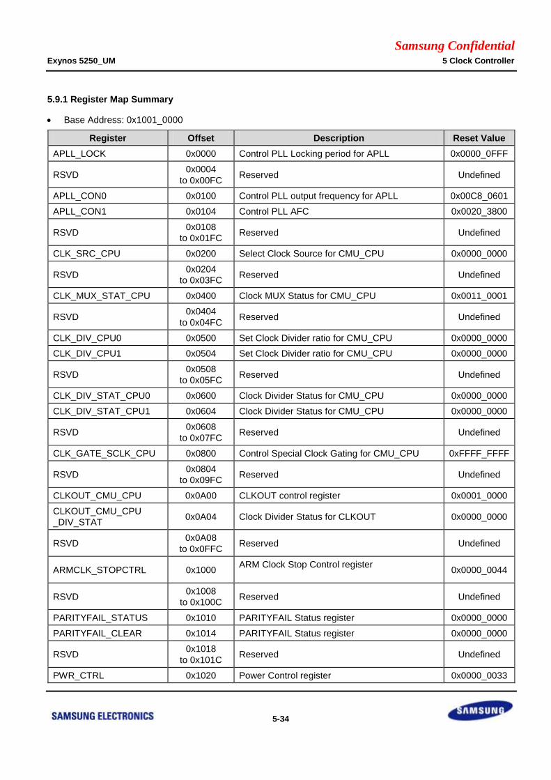
Samsung Confidential Exynos 5250_UM 5 Clock Controller
5-34
5.9.1 Register Map Summary
Base Address: 0x1001_0000
Register Offset Description Reset Value
APLL_LOCK 0x0000 Control PLL Locking period for APLL 0x0000_0FFF
RSVD 0x0004
to 0x00FC Reserved Undefined
APLL_CON0 0x0100 Control PLL output frequency for APLL 0x00C8_0601
APLL_CON1 0x0104 Control PLL AFC 0x0020_3800
RSVD 0x0108
to 0x01FC Reserved Undefined
CLK_SRC_CPU 0x0200 Select Clock Source for CMU_CPU 0x0000_0000
RSVD 0x0204
to 0x03FC Reserved Undefined
CLK_MUX_STAT_CPU 0x0400 Clock MUX Status for CMU_CPU 0x0011_0001
RSVD 0x0404
to 0x04FC Reserved Undefined
CLK_DIV_CPU0 0x0500 Set Clock Divider ratio for CMU_CPU 0x0000_0000
CLK_DIV_CPU1 0x0504 Set Clock Divider ratio for CMU_CPU 0x0000_0000
RSVD 0x0508
to 0x05FC Reserved Undefined
CLK_DIV_STAT_CPU0 0x0600 Clock Divider Status for CMU_CPU 0x0000_0000
CLK_DIV_STAT_CPU1 0x0604 Clock Divider Status for CMU_CPU 0x0000_0000
RSVD 0x0608
to 0x07FC Reserved Undefined
CLK_GATE_SCLK_CPU 0x0800 Control Special Clock Gating for CMU_CPU 0xFFFF_FFFF
RSVD 0x0804
to 0x09FC Reserved Undefined
CLKOUT_CMU_CPU 0x0A00 CLKOUT control register 0x0001_0000
CLKOUT_CMU_CPU
_DIV_STAT 0x0A04 Clock Divider Status for CLKOUT 0x0000_0000
RSVD 0x0A08
to 0x0FFC Reserved Undefined
ARMCLK_STOPCTRL 0x1000 ARM Clock Stop Control register
0x0000_0044
RSVD 0x1008
to 0x100C Reserved Undefined
PARITYFAIL_STATUS 0x1010 PARITYFAIL Status register 0x0000_0000
PARITYFAIL_CLEAR 0x1014 PARITYFAIL Status register 0x0000_0000
RSVD 0x1018
to 0x101C Reserved Undefined
PWR_CTRL 0x1020 Power Control register 0x0000_0033
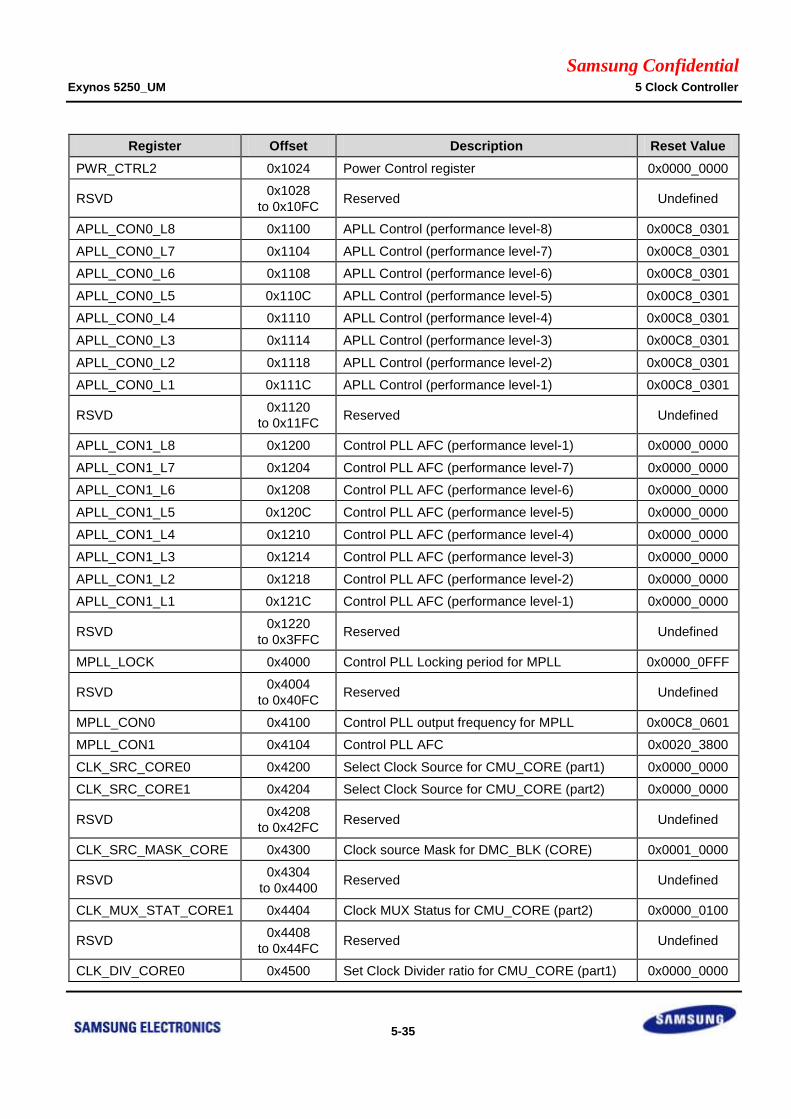
Samsung Confidential Exynos 5250_UM 5 Clock Controller
5-35
Register Offset Description Reset Value
PWR_CTRL2 0x1024 Power Control register 0x0000_0000
RSVD 0x1028
to 0x10FC Reserved Undefined
APLL_CON0_L8 0x1100 APLL Control (performance level-8) 0x00C8_0301
APLL_CON0_L7 0x1104 APLL Control (performance level-7) 0x00C8_0301
APLL_CON0_L6 0x1108 APLL Control (performance level-6) 0x00C8_0301
APLL_CON0_L5 0x110C APLL Control (performance level-5) 0x00C8_0301
APLL_CON0_L4 0x1110 APLL Control (performance level-4) 0x00C8_0301
APLL_CON0_L3 0x1114 APLL Control (performance level-3) 0x00C8_0301
APLL_CON0_L2 0x1118 APLL Control (performance level-2) 0x00C8_0301
APLL_CON0_L1 0x111C APLL Control (performance level-1) 0x00C8_0301
RSVD 0x1120
to 0x11FC Reserved Undefined
APLL_CON1_L8 0x1200 Control PLL AFC (performance level-1) 0x0000_0000
APLL_CON1_L7 0x1204 Control PLL AFC (performance level-7) 0x0000_0000
APLL_CON1_L6 0x1208 Control PLL AFC (performance level-6) 0x0000_0000
APLL_CON1_L5 0x120C Control PLL AFC (performance level-5) 0x0000_0000
APLL_CON1_L4 0x1210 Control PLL AFC (performance level-4) 0x0000_0000
APLL_CON1_L3 0x1214 Control PLL AFC (performance level-3) 0x0000_0000
APLL_CON1_L2 0x1218 Control PLL AFC (performance level-2) 0x0000_0000
APLL_CON1_L1 0x121C Control PLL AFC (performance level-1) 0x0000_0000
RSVD 0x1220
to 0x3FFC Reserved Undefined
MPLL_LOCK 0x4000 Control PLL Locking period for MPLL 0x0000_0FFF
RSVD 0x4004
to 0x40FC Reserved Undefined
MPLL_CON0 0x4100 Control PLL output frequency for MPLL 0x00C8_0601
MPLL_CON1 0x4104 Control PLL AFC 0x0020_3800
CLK_SRC_CORE0 0x4200 Select Clock Source for CMU_CORE (part1) 0x0000_0000
CLK_SRC_CORE1 0x4204 Select Clock Source for CMU_CORE (part2) 0x0000_0000
RSVD 0x4208
to 0x42FC Reserved Undefined
CLK_SRC_MASK_CORE 0x4300 Clock source Mask for DMC_BLK (CORE) 0x0001_0000
RSVD 0x4304
to 0x4400 Reserved Undefined
CLK_MUX_STAT_CORE1 0x4404 Clock MUX Status for CMU_CORE (part2) 0x0000_0100
RSVD 0x4408
to 0x44FC Reserved Undefined
CLK_DIV_CORE0 0x4500 Set Clock Divider ratio for CMU_CORE (part1) 0x0000_0000
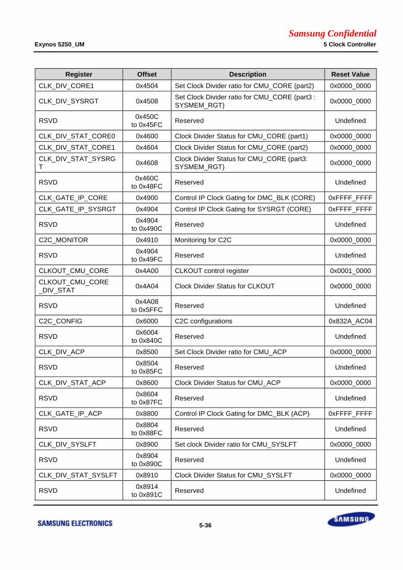
Samsung Confidential Exynos 5250_UM 5 Clock Controller
5-36
Register Offset Description Reset Value
CLK_DIV_CORE1 0x4504 Set Clock Divider ratio for CMU_CORE (part2) 0x0000_0000
CLK_DIV_SYSRGT 0x4508 Set Clock Divider ratio for CMU_CORE (part3 :
SYSMEM_RGT) 0x0000_0000
RSVD 0x450C
to 0x45FC Reserved Undefined
CLK_DIV_STAT_CORE0 0x4600 Clock Divider Status for CMU_CORE (part1) 0x0000_0000
CLK_DIV_STAT_CORE1 0x4604 Clock Divider Status for CMU_CORE (part2) 0x0000_0000
CLK_DIV_STAT_SYSRG
T 0x4608
Clock Divider Status for CMU_CORE (part3:
SYSMEM_RGT) 0x0000_0000
RSVD 0x460C
to 0x48FC Reserved Undefined
CLK_GATE_IP_CORE 0x4900 Control IP Clock Gating for DMC_BLK (CORE) 0xFFFF_FFFF
CLK_GATE_IP_SYSRGT 0x4904 Control IP Clock Gating for SYSRGT (CORE) 0xFFFF_FFFF
RSVD 0x4904
to 0x490C Reserved Undefined
C2C_MONITOR 0x4910 Monitoring for C2C 0x0000_0000
RSVD 0x4904
to 0x49FC Reserved Undefined
CLKOUT_CMU_CORE 0x4A00 CLKOUT control register 0x0001_0000
CLKOUT_CMU_CORE
_DIV_STAT 0x4A04 Clock Divider Status for CLKOUT 0x0000_0000
RSVD 0x4A08
to 0x5FFC Reserved Undefined
C2C_CONFIG 0x6000 C2C configurations 0x832A_AC04
RSVD 0x6004
to 0x840C Reserved Undefined
CLK_DIV_ACP 0x8500 Set Clock Divider ratio for CMU_ACP 0x0000_0000
RSVD 0x8504
to 0x85FC Reserved Undefined
CLK_DIV_STAT_ACP 0x8600 Clock Divider Status for CMU_ACP 0x0000_0000
RSVD 0x8604
to 0x87FC Reserved Undefined
CLK_GATE_IP_ACP 0x8800 Control IP Clock Gating for DMC_BLK (ACP) 0xFFFF_FFFF
RSVD 0x8804
to 0x88FC Reserved Undefined
CLK_DIV_SYSLFT 0x8900 Set clock Divider ratio for CMU_SYSLFT 0x0000_0000
RSVD 0x8904
to 0x890C Reserved Undefined
CLK_DIV_STAT_SYSLFT 0x8910 Clock Divider Status for CMU_SYSLFT 0x0000_0000
RSVD 0x8914
to 0x891C Reserved Undefined
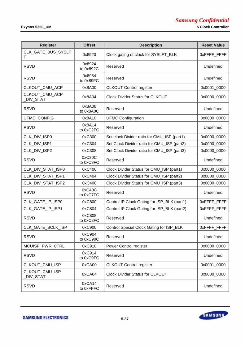
Samsung Confidential Exynos 5250_UM 5 Clock Controller
5-37
Register Offset Description Reset Value
CLK_GATE_BUS_SYSLF
T 0x8920 Clock gating of clock for SYSLFT_BLK 0xFFFF_FFFF
RSVD 0x8924
to 0x892C Reserved Undefined
RSVD 0x8934
to 0x89FC Reserved Undefined
CLKOUT_CMU_ACP 0x8A00 CLKOUT Control register 0x0001_0000
CLKOUT_CMU_ACP
_DIV_STAT 0x8A04 Clock Divider Status for CLKOUT 0x0000_0000
RSVD 0x8A08
to 0x8A0C Reserved Undefined
UFMC_CONFIG 0x8A10 UFMC Configuration 0x0000_0000
RSVD 0x8A14
to 0xC2FC Reserved Undefined
CLK_DIV_ISP0 0xC300 Set clock Divider ratio for CMU_ISP (part1) 0x0000_0000
CLK_DIV_ISP1 0xC304 Set Clock Divider ratio for CMU_ISP (part2) 0x0000_0000
CLK_DIV_ISP2 0xC308 Set Clock Divider ratio for CMU_ISP (part3) 0x0000_0000
RSVD 0xC30C
to 0xC3FC Reserved Undefined
CLK_DIV_STAT_ISP0 0xC400 Clock Divider Status for CMU_ISP (part1) 0x0000_0000
CLK_DIV_STAT_ISP1 0xC404 Clock Divider Status for CMU_ISP (part2) 0x0000_0000
CLK_DIV_STAT_ISP2 0xC408 Clock Divider Status for CMU_ISP (part3) 0x0000_0000
RSVD 0xC40C
to 0xC7FC Reserved Undefined
CLK_GATE_IP_ISP0 0xC800 Control IP Clock Gating for ISP_BLK (part1) 0xFFFF_FFFF
CLK_GATE_IP_ISP1 0xC804 Control IP Clock Gating for ISP_BLK (part2) 0xFFFF_FFFF
RSVD 0xC808
to 0xC8FC Reserved Undefined
CLK_GATE_SCLK_ISP 0xC900 Control Special Clock Gating for ISP_BLK 0xFFFF_FFFF
RSVD 0xC904
to 0xC90C Reserved Undefined
MCUISP_PWR_CTRL 0xC910 Power Control register 0x0000_0000
RSVD 0xC914
to 0xC9FC Reserved Undefined
CLKOUT_CMU_ISP 0xCA00 CLKOUT Control register 0x0001_0000
CLKOUT_CMU_ISP
_DIV_STAT 0xCA04 Clock Divider Status for CLKOUT 0x0000_0000
RSVD 0xCA14
to 0xFFFC Reserved Undefined
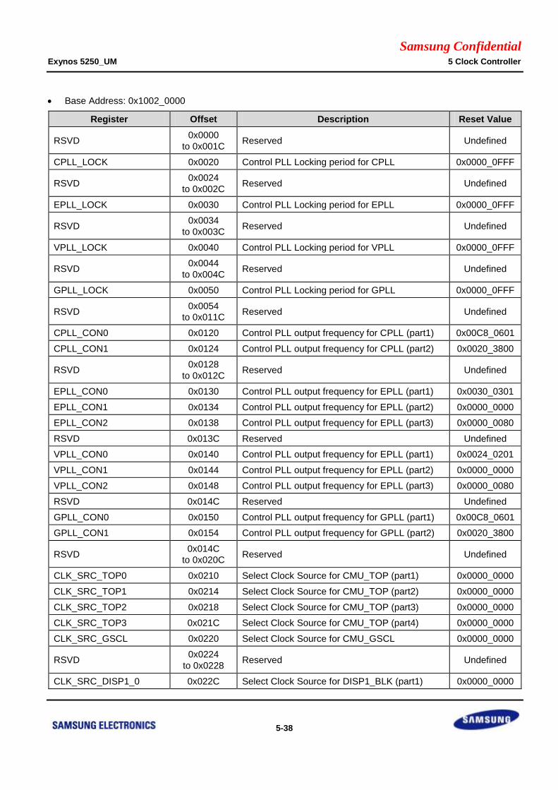
Samsung Confidential Exynos 5250_UM 5 Clock Controller
5-38
Base Address: 0x1002_0000
Register Offset Description Reset Value
RSVD 0x0000
to 0x001C Reserved Undefined
CPLL_LOCK 0x0020 Control PLL Locking period for CPLL 0x0000_0FFF
RSVD 0x0024
to 0x002C Reserved Undefined
EPLL_LOCK 0x0030 Control PLL Locking period for EPLL 0x0000_0FFF
RSVD 0x0034
to 0x003C Reserved Undefined
VPLL_LOCK 0x0040 Control PLL Locking period for VPLL 0x0000_0FFF
RSVD 0x0044
to 0x004C Reserved Undefined
GPLL_LOCK 0x0050 Control PLL Locking period for GPLL 0x0000_0FFF
RSVD 0x0054
to 0x011C Reserved Undefined
CPLL_CON0 0x0120 Control PLL output frequency for CPLL (part1) 0x00C8_0601
CPLL_CON1 0x0124 Control PLL output frequency for CPLL (part2) 0x0020_3800
RSVD 0x0128
to 0x012C Reserved Undefined
EPLL_CON0 0x0130 Control PLL output frequency for EPLL (part1) 0x0030_0301
EPLL_CON1 0x0134 Control PLL output frequency for EPLL (part2) 0x0000_0000
EPLL_CON2 0x0138 Control PLL output frequency for EPLL (part3) 0x0000_0080
RSVD 0x013C Reserved Undefined
VPLL_CON0 0x0140 Control PLL output frequency for EPLL (part1) 0x0024_0201
VPLL_CON1 0x0144 Control PLL output frequency for EPLL (part2) 0x0000_0000
VPLL_CON2 0x0148 Control PLL output frequency for EPLL (part3) 0x0000_0080
RSVD 0x014C Reserved Undefined
GPLL_CON0 0x0150 Control PLL output frequency for GPLL (part1) 0x00C8_0601
GPLL_CON1 0x0154 Control PLL output frequency for GPLL (part2) 0x0020_3800
RSVD 0x014C
to 0x020C Reserved Undefined
CLK_SRC_TOP0 0x0210 Select Clock Source for CMU_TOP (part1) 0x0000_0000
CLK_SRC_TOP1 0x0214 Select Clock Source for CMU_TOP (part2) 0x0000_0000
CLK_SRC_TOP2 0x0218 Select Clock Source for CMU_TOP (part3) 0x0000_0000
CLK_SRC_TOP3 0x021C Select Clock Source for CMU_TOP (part4) 0x0000_0000
CLK_SRC_GSCL 0x0220 Select Clock Source for CMU_GSCL 0x0000_0000
RSVD 0x0224
to 0x0228 Reserved Undefined
CLK_SRC_DISP1_0 0x022C Select Clock Source for DISP1_BLK (part1) 0x0000_0000
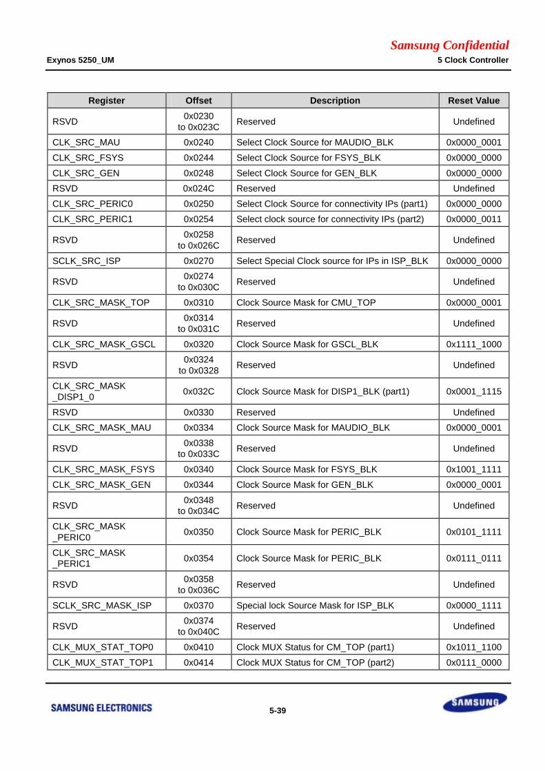
Samsung Confidential Exynos 5250_UM 5 Clock Controller
5-39
Register Offset Description Reset Value
RSVD 0x0230
to 0x023C Reserved Undefined
CLK_SRC_MAU 0x0240 Select Clock Source for MAUDIO_BLK 0x0000_0001
CLK_SRC_FSYS 0x0244 Select Clock Source for FSYS_BLK 0x0000_0000
CLK_SRC_GEN 0x0248 Select Clock Source for GEN_BLK 0x0000_0000
RSVD 0x024C Reserved Undefined
CLK_SRC_PERIC0 0x0250 Select Clock Source for connectivity IPs (part1) 0x0000_0000
CLK_SRC_PERIC1 0x0254 Select clock source for connectivity IPs (part2) 0x0000_0011
RSVD 0x0258
to 0x026C Reserved Undefined
SCLK_SRC_ISP 0x0270 Select Special Clock source for IPs in ISP_BLK 0x0000_0000
RSVD 0x0274
to 0x030C Reserved Undefined
CLK_SRC_MASK_TOP 0x0310 Clock Source Mask for CMU_TOP 0x0000_0001
RSVD 0x0314
to 0x031C Reserved Undefined
CLK_SRC_MASK_GSCL 0x0320 Clock Source Mask for GSCL_BLK 0x1111_1000
RSVD 0x0324
to 0x0328 Reserved Undefined
CLK_SRC_MASK
_DISP1_0 0x032C Clock Source Mask for DISP1_BLK (part1) 0x0001_1115
RSVD 0x0330 Reserved Undefined
CLK_SRC_MASK_MAU 0x0334 Clock Source Mask for MAUDIO_BLK 0x0000_0001
RSVD 0x0338
to 0x033C Reserved Undefined
CLK_SRC_MASK_FSYS 0x0340 Clock Source Mask for FSYS_BLK 0x1001_1111
CLK_SRC_MASK_GEN 0x0344 Clock Source Mask for GEN_BLK 0x0000_0001
RSVD 0x0348
to 0x034C Reserved Undefined
CLK_SRC_MASK
_PERIC0 0x0350 Clock Source Mask for PERIC_BLK 0x0101_1111
CLK_SRC_MASK
_PERIC1 0x0354 Clock Source Mask for PERIC_BLK 0x0111_0111
RSVD 0x0358
to 0x036C Reserved Undefined
SCLK_SRC_MASK_ISP 0x0370 Special lock Source Mask for ISP_BLK 0x0000_1111
RSVD 0x0374
to 0x040C Reserved Undefined
CLK_MUX_STAT_TOP0 0x0410 Clock MUX Status for CM_TOP (part1) 0x1011_1100
CLK_MUX_STAT_TOP1 0x0414 Clock MUX Status for CM_TOP (part2) 0x0111_0000
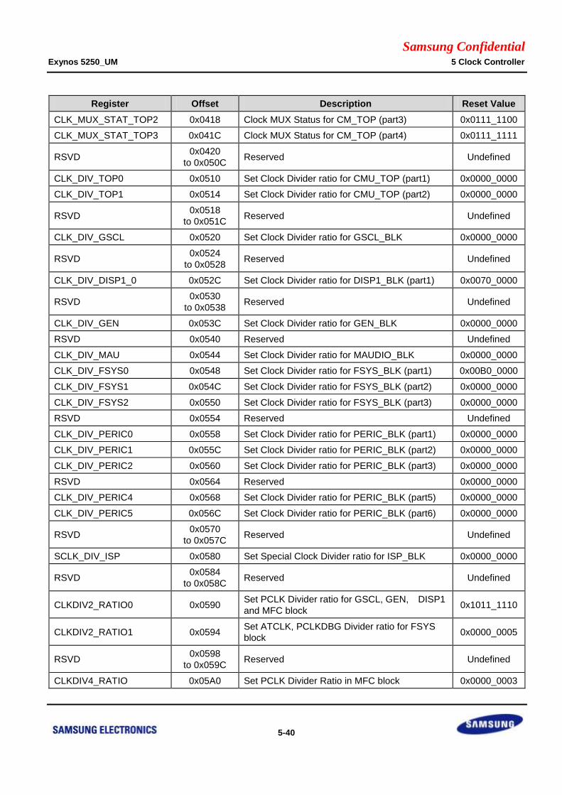
Samsung Confidential Exynos 5250_UM 5 Clock Controller
5-40
Register Offset Description Reset Value
CLK_MUX_STAT_TOP2 0x0418 Clock MUX Status for CM_TOP (part3) 0x0111_1100
CLK_MUX_STAT_TOP3 0x041C Clock MUX Status for CM_TOP (part4) 0x0111_1111
RSVD 0x0420
to 0x050C Reserved Undefined
CLK_DIV_TOP0 0x0510 Set Clock Divider ratio for CMU_TOP (part1) 0x0000_0000
CLK_DIV_TOP1 0x0514 Set Clock Divider ratio for CMU_TOP (part2) 0x0000_0000
RSVD 0x0518
to 0x051C Reserved Undefined
CLK_DIV_GSCL 0x0520 Set Clock Divider ratio for GSCL_BLK 0x0000_0000
RSVD 0x0524
to 0x0528 Reserved Undefined
CLK_DIV_DISP1_0 0x052C Set Clock Divider ratio for DISP1_BLK (part1) 0x0070_0000
RSVD 0x0530
to 0x0538 Reserved Undefined
CLK_DIV_GEN 0x053C Set Clock Divider ratio for GEN_BLK 0x0000_0000
RSVD 0x0540 Reserved Undefined
CLK_DIV_MAU 0x0544 Set Clock Divider ratio for MAUDIO_BLK 0x0000_0000
CLK_DIV_FSYS0 0x0548 Set Clock Divider ratio for FSYS_BLK (part1) 0x00B0_0000
CLK_DIV_FSYS1 0x054C Set Clock Divider ratio for FSYS_BLK (part2) 0x0000_0000
CLK_DIV_FSYS2 0x0550 Set Clock Divider ratio for FSYS_BLK (part3) 0x0000_0000
RSVD 0x0554 Reserved Undefined
CLK_DIV_PERIC0 0x0558 Set Clock Divider ratio for PERIC_BLK (part1) 0x0000_0000
CLK_DIV_PERIC1 0x055C Set Clock Divider ratio for PERIC_BLK (part2) 0x0000_0000
CLK_DIV_PERIC2 0x0560 Set Clock Divider ratio for PERIC_BLK (part3) 0x0000_0000
RSVD 0x0564 Reserved 0x0000_0000
CLK_DIV_PERIC4 0x0568 Set Clock Divider ratio for PERIC_BLK (part5) 0x0000_0000
CLK_DIV_PERIC5 0x056C Set Clock Divider ratio for PERIC_BLK (part6) 0x0000_0000
RSVD 0x0570
to 0x057C Reserved Undefined
SCLK_DIV_ISP 0x0580 Set Special Clock Divider ratio for ISP_BLK 0x0000_0000
RSVD 0x0584
to 0x058C Reserved Undefined
CLKDIV2_RATIO0 0x0590 Set PCLK Divider ratio for GSCL, GEN, DISP1
and MFC block 0x1011_1110
CLKDIV2_RATIO1 0x0594 Set ATCLK, PCLKDBG Divider ratio for FSYS
block 0x0000_0005
RSVD 0x0598
to 0x059C Reserved Undefined
CLKDIV4_RATIO 0x05A0 Set PCLK Divider Ratio in MFC block 0x0000_0003

Samsung Confidential Exynos 5250_UM 5 Clock Controller
5-41
Register Offset Description Reset Value
RSVD 0x05A4
to 0x060C Reserved Undefined
CLK_DIV_STAT_TOP0 0x0610 Clock Divider Status for CMU_TOP (part1) 0x0000_0000
CLK_DIV_STAT_TOP1 0x0614 Clock Divider Status for CMU_TOP (part2) 0x0000_0000
RSVD 0x0618
to 0x061C Reserved Undefined
CLK_DIV_STAT_GSCL 0x0620 Clock Divider Status for GSCL_BLK 0x0000_0000
RSVD 0x0624
to 0x0628 Reserved Undefined
CLK_DIV_STAT_DISP1_0 0x062C Clock Divider Status for DISP1_BLK (part1) 0x0000_0000
RSVD 0x0630
to 0x0638 Reserved Undefined
CLK_DIV_STAT_GEN 0x063C Clock Divider Status for GEN_BLK 0x0000_0000
RSVD 0x0640 Reserved Undefined
CLK_DIV_STAT_MAU 0x0644 Clock Divider Status for MAUDIO_BLK 0x0000_0000
CLK_DIV_STAT_FSYS0 0x0648 Clock Divider Status for FSYS_BLK (part1) 0x0000_0000
CLK_DIV_STAT_FSYS1 0x064C Clock Divider Status for FSYS_BLK (part2) 0x0000_0000
CLK_DIV_STAT_FSYS2 0x0650 Clock Divider Status for FSYS_BLK (part3) 0x0000_0000
RSVD 0x0654 Reserved Undefined
CLK_DIV_STAT_PERIC0 0x0658 Clock Divider Status for PERIC_BLK (part1) 0x0000_0000
CLK_DIV_STAT_PERIC1 0x065C Clock Divider Status for PERIC_BLK (part2) 0x0000_0000
CLK_DIV_STAT_PERIC2 0x0660 Clock Divider Status for PERIC_BLK (part3) 0x0000_0000
CLK_DIV_STAT_PERIC3 0x0664 Clock Divider Status for PERIC_BLK (part4) 0x0000_0000
CLK_DIV_STAT_PERIC4 0x0668 Clock Divider Status for PERIC_BLK (part5) 0x0000_0000
CLK_DIV_STAT_PERIC5 0x066C Clock Divider Status for PERIC_BLK (part6) 0x0000_0000
RSVD 0x0670
to 0x067C Reserved Undefined
SCLK_DIV_STAT_ISP 0x0680 Special Clock Divider Status for ISP_BLK 0x0000_0000
RSVD 0x0684
to 0x068C Reserved Undefined
CLKDIV2_STAT0 0x0690 PCLK Divider Status for GSCL, GEN, DISP1
and MFC block 0x0000_0000
CLKDIV2_STAT1 0x0694 ATCLK, PCLKDBG Divider Status for FSYS
block 0x0000_0000
RSVD 0x0698
to 0x069C Reserved Undefined
CLKDIV4_STAT 0x06A0 PCLK Divider Status for MFC block 0x0000_0000
RSVD 0x06A4
to 0x0820 Reserved Undefined
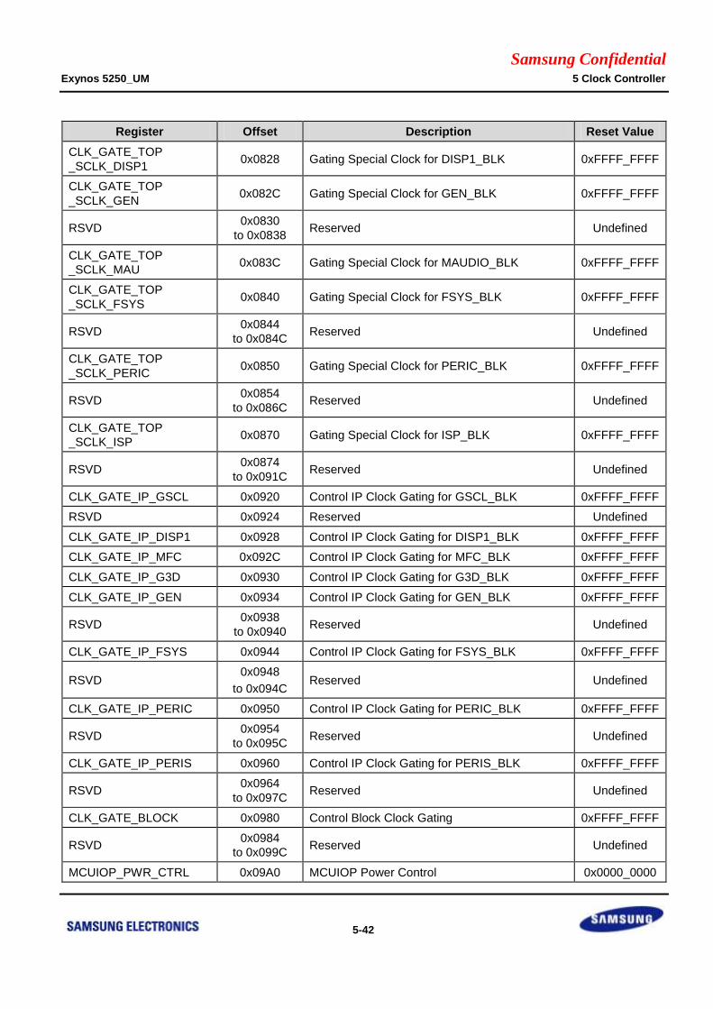
Samsung Confidential Exynos 5250_UM 5 Clock Controller
5-42
Register Offset Description Reset Value
CLK_GATE_TOP
_SCLK_DISP1 0x0828 Gating Special Clock for DISP1_BLK 0xFFFF_FFFF
CLK_GATE_TOP
_SCLK_GEN 0x082C Gating Special Clock for GEN_BLK 0xFFFF_FFFF
RSVD 0x0830
to 0x0838 Reserved Undefined
CLK_GATE_TOP
_SCLK_MAU 0x083C Gating Special Clock for MAUDIO_BLK 0xFFFF_FFFF
CLK_GATE_TOP
_SCLK_FSYS 0x0840 Gating Special Clock for FSYS_BLK 0xFFFF_FFFF
RSVD 0x0844
to 0x084C Reserved Undefined
CLK_GATE_TOP
_SCLK_PERIC 0x0850 Gating Special Clock for PERIC_BLK 0xFFFF_FFFF
RSVD 0x0854
to 0x086C Reserved Undefined
CLK_GATE_TOP
_SCLK_ISP 0x0870 Gating Special Clock for ISP_BLK 0xFFFF_FFFF
RSVD 0x0874
to 0x091C Reserved Undefined
CLK_GATE_IP_GSCL 0x0920 Control IP Clock Gating for GSCL_BLK 0xFFFF_FFFF
RSVD 0x0924 Reserved Undefined
CLK_GATE_IP_DISP1 0x0928 Control IP Clock Gating for DISP1_BLK 0xFFFF_FFFF
CLK_GATE_IP_MFC 0x092C Control IP Clock Gating for MFC_BLK 0xFFFF_FFFF
CLK_GATE_IP_G3D 0x0930 Control IP Clock Gating for G3D_BLK 0xFFFF_FFFF
CLK_GATE_IP_GEN 0x0934 Control IP Clock Gating for GEN_BLK 0xFFFF_FFFF
RSVD 0x0938
to 0x0940 Reserved Undefined
CLK_GATE_IP_FSYS 0x0944 Control IP Clock Gating for FSYS_BLK 0xFFFF_FFFF
RSVD 0x0948
to 0x094C Reserved Undefined
CLK_GATE_IP_PERIC 0x0950 Control IP Clock Gating for PERIC_BLK 0xFFFF_FFFF
RSVD 0x0954
to 0x095C Reserved Undefined
CLK_GATE_IP_PERIS 0x0960 Control IP Clock Gating for PERIS_BLK 0xFFFF_FFFF
RSVD 0x0964
to 0x097C Reserved Undefined
CLK_GATE_BLOCK 0x0980 Control Block Clock Gating 0xFFFF_FFFF
RSVD 0x0984
to 0x099C Reserved Undefined
MCUIOP_PWR_CTRL 0x09A0 MCUIOP Power Control 0x0000_0000
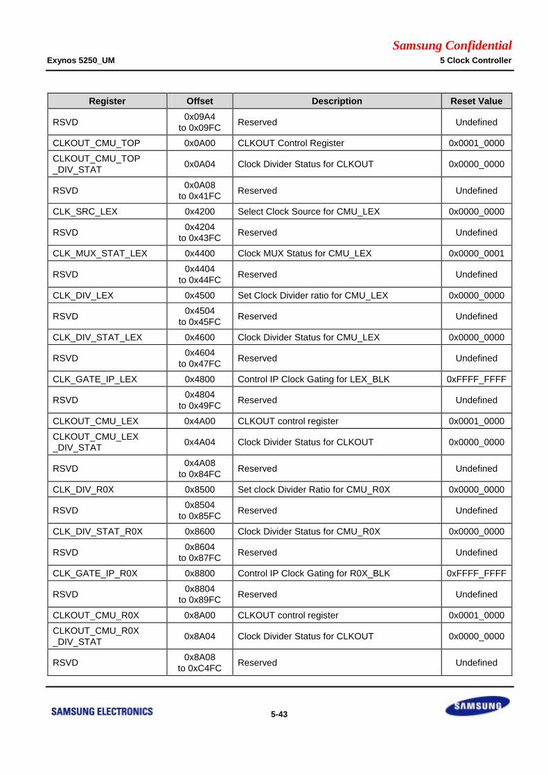
Samsung Confidential Exynos 5250_UM 5 Clock Controller
5-43
Register Offset Description Reset Value
RSVD 0x09A4
to 0x09FC Reserved Undefined
CLKOUT_CMU_TOP 0x0A00 CLKOUT Control Register 0x0001_0000
CLKOUT_CMU_TOP
_DIV_STAT 0x0A04 Clock Divider Status for CLKOUT 0x0000_0000
RSVD 0x0A08
to 0x41FC Reserved Undefined
CLK_SRC_LEX 0x4200 Select Clock Source for CMU_LEX 0x0000_0000
RSVD 0x4204
to 0x43FC Reserved Undefined
CLK_MUX_STAT_LEX 0x4400 Clock MUX Status for CMU_LEX 0x0000_0001
RSVD 0x4404
to 0x44FC Reserved Undefined
CLK_DIV_LEX 0x4500 Set Clock Divider ratio for CMU_LEX 0x0000_0000
RSVD 0x4504
to 0x45FC Reserved Undefined
CLK_DIV_STAT_LEX 0x4600 Clock Divider Status for CMU_LEX 0x0000_0000
RSVD 0x4604
to 0x47FC Reserved Undefined
CLK_GATE_IP_LEX 0x4800 Control IP Clock Gating for LEX_BLK 0xFFFF_FFFF
RSVD 0x4804
to 0x49FC Reserved Undefined
CLKOUT_CMU_LEX 0x4A00 CLKOUT control register 0x0001_0000
CLKOUT_CMU_LEX
_DIV_STAT 0x4A04 Clock Divider Status for CLKOUT 0x0000_0000
RSVD 0x4A08
to 0x84FC Reserved Undefined
CLK_DIV_R0X 0x8500 Set clock Divider Ratio for CMU_R0X 0x0000_0000
RSVD 0x8504
to 0x85FC Reserved Undefined
CLK_DIV_STAT_R0X 0x8600 Clock Divider Status for CMU_R0X 0x0000_0000
RSVD 0x8604
to 0x87FC Reserved Undefined
CLK_GATE_IP_R0X 0x8800 Control IP Clock Gating for R0X_BLK 0xFFFF_FFFF
RSVD 0x8804
to 0x89FC Reserved Undefined
CLKOUT_CMU_R0X 0x8A00 CLKOUT control register 0x0001_0000
CLKOUT_CMU_R0X
_DIV_STAT 0x8A04 Clock Divider Status for CLKOUT 0x0000_0000
RSVD 0x8A08
to 0xC4FC Reserved Undefined
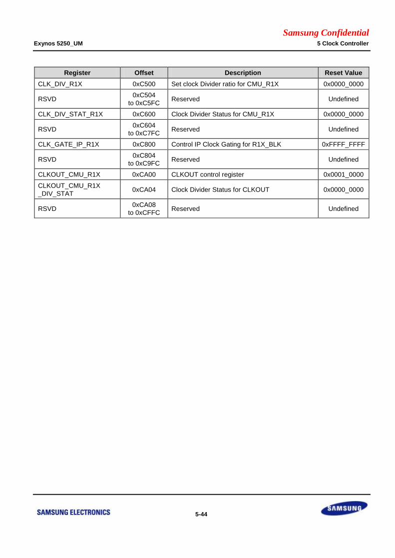
Samsung Confidential Exynos 5250_UM 5 Clock Controller
5-44
Register Offset Description Reset Value
CLK_DIV_R1X 0xC500 Set clock Divider ratio for CMU_R1X 0x0000_0000
RSVD 0xC504
to 0xC5FC Reserved Undefined
CLK_DIV_STAT_R1X 0xC600 Clock Divider Status for CMU_R1X 0x0000_0000
RSVD 0xC604
to 0xC7FC Reserved Undefined
CLK_GATE_IP_R1X 0xC800 Control IP Clock Gating for R1X_BLK 0xFFFF_FFFF
RSVD 0xC804
to 0xC9FC Reserved Undefined
CLKOUT_CMU_R1X 0xCA00 CLKOUT control register 0x0001_0000
CLKOUT_CMU_R1X
_DIV_STAT 0xCA04 Clock Divider Status for CLKOUT 0x0000_0000
RSVD 0xCA08
to 0xCFFC Reserved Undefined

Samsung Confidential Exynos 5250_UM 5 Clock Controller
5-45
Base Address: 0x1003_0000
Register Offset Description Reset Value
RSVD 0x0000
to 0x000C Reserved Undefined
BPLL_LOCK 0x0010 Control PLL Locking period of BPLL 0x0000_0FFF
RSVD 0x0014
to 0x010C Reserved Undefined
BPLL_CON0 0x0110 Control PLL output frequency for BPLL 0x00C8_0601
BPLL_CON1 0x0114 Control PLL AFC 0x0020_3800
RSVD 0x0118
to 0x01FC Reserved Undefined
CLK_SRC_CDREX 0x0200 Select Clock Source for CMU_CDREX 0x0000_0000
RSVD 0x0204
to 0x03FC Reserved Undefined
CLK_MUX_STAT
_CDREX 0x0400 Clock MUX Status for CMU_CDREX 0x0000_1111
RSVD 0x0404
to 0x04FC Reserved Undefined
CLK_DIV_CDREX 0x0500 Set Clock Divider ratio for CMU_CDREX 0x0000_0000
RSVD 0x0504
to 0x05FC Reserved Undefined
CLK_DIV_STAT
_CDREX 0x0600 Clock Divider Status for CMU_CDREX 0x0000_0000
RSVD 0x0604
to 0x08FC Reserved Undefined
CLK_GATE_IP_CDREX 0x0900 Control IP Clock Gating for DMC_BLK (CDREX) 0xFFFF_FFFF
RSVD 0x0904
to 0x090C Reserved Undefined
RSVD 0x0904
to 0x0910 Reserved Undefined
DMC_FREQ_CTRL 0x0914 DMC Frequency Control register 0x0000_0000
RSVD 0x0918
to 0x0918 Reserved Undefined
DREX2_PAUSE 0x091C Pause function for DREX2 0x7FFC_7FFF
RSVD 0x0920
to 0x09FC Reserved Undefined
CLKOUT_CMU
_CDREX 0x0A00 CLKOUT control register 0x0001_0000
CLKOUT_CMU
_CDREX_DIV_STAT 0x0A04 Clock Divider Status for CLKOUT 0x0000_0000
RSVD 0x0A08
to 0x0A0C Reserved Undefined

Samsung Confidential Exynos 5250_UM 5 Clock Controller
5-46
Register Offset Description Reset Value
LPDDR3PHY_CTRL 0x0A10 Reset for LPDDR3HPHY. This reset is used for
DDR3 memory 0x0000_0001
RSVD 0x0A14
to 0x0A1C Reserved Undefined
LPDDR3PHY_CON3 0x0A20 DREX ADDR pin Change 0x0000_0000
PLL_DIV2_SEL 0x0A24 Selection for PLL_FOUT 0x0000_0000
RSVD 0x0A28
to 0xFFFC Reserved Undefined
Samsung Confidential Exynos 5250_UM 5 Clock Controller
5-47
SFRs consist of nine parts.
The SFRs with address 0x1001_0000 to 0x1001_3FFF control clock-related logics for CPU block. They
control APLL, Clock Source Selection, and Clock Divider Ratio for CPU-related logics.
The SFRs with address 0x1001_4000 to 0x1001_7FFF control clock-related logics for DMC block (part 1).
They control MPLL, Clock Source Selection, Clock Divider Ratio, and Clock Gating for DMC peripheral sub-
block.
The SFRs with address 0x1001_8000 to 0x1001_BFFF control clock-related logics for DMC block (part 2).
They control Clock Source Selection, Clock Divider Ratio, and Clock Gating for ACP sub-block.
The SFRs with address 0x1001_C000 to 0x1001_FFFF control clock-related logics for ISP block.
They control Clock Source Selection, Clock Divider Ratio, and Clock Gating.
The SFRs with address 0x1002_0000 to 0x1002_3FFF control clock-related logics for MFC, G3D, DISP1,
GSCL, FSYS, PERIC, and PERIS blocks. They control CPLL, EPLL, GPLL and VPLL, Clock Source
Selection, Clock Divider Ratio, and Clock Gating.
The SFRs with address 0x1002_4000 to 0x1002_7FFF control clock-related logics for LEX block.
They control Clock Source Selection, Clock Divider Ratio, and Clock Gating.
The SFRs with address 0x1002_8000 to 0x1002_BFFF control clock-related logics for R0X block.
They control Clock Source Selection, Clock Divider Ratio, and Clock Gating.
The SFRs with address 0x1002_C000 to 0x1002_FFFF control clock-related logics for R1X block.
They control Clock Source Selection, Clock Divider Ratio, and Clock Gating.
The SFRs with address 0x1003_0000 to 0x1003_3FFF control clock-related logics for DMC block (part 3).
They control BPLL, Clock Source Selection, Clock Divider Ratio, and Clock Gating for DREXII in CDREX sub-
block.

Samsung Confidential Exynos 5250_UM 5 Clock Controller
5-48
5.9.1.1 APLL_LOCK
Base Address: 0x1001_0000
Address = Base Address + 0x0000, Reset Value = 0x0000_0FFF
Name Bit Type Description Reset Value
RSVD [31:20] – Reserved 0x0
PLL_LOCKTIME [19:0] RW
Required period(in cycles) to generate a stable
clock output
The maximum lock time can be up to 250 PDIV
cycles of PLL's FIN (XXTI).
0xF_FFFF

Samsung Confidential Exynos 5250_UM 5 Clock Controller
5-49
5.9.1.2 APLL_CON0
Base Address: 0x1001_0000
Address = Base Address + 0x0100, Reset Value = 0x00C8_0601
Name Bit Type Description Reset Value
ENABLE [31] RW
PLL Enable control
0 = Disables PLL
1 = Enables PLL
0x0
RSVD [30] – Reserved 0x0
LOCKED [29] R
PLL Locking indication
0 = Unlocks PLL
1 = Locks PLL
0x0
RSVD [28] – Reserved 0x0
FSEL [27] RW
Monitoring Frequency Select pin
0 = FVCO_OUT = FREF
1 = FVCO_OUT = FVCO
0x0
RSVD [26] – Reserved 0x0
MDIV [25:16] RW PLL M Divide value 0xC8
RSVD [15:14] – Reserved 0x0
PDIV [13:8] RW PLL P Divide value 0x6
RSVD [7:3] – Reserved 0x0
SDIV [2:0] RW PLL S Divide value 0x1
The reset value of APLL_CON0 generates 400 MHz output clock for the input clock frequency of 24 MHz.
Equation to calculate the output frequency is:
FOUT = MDIV FIN/(PDIV 2SDIV
)
MDIV, PDIV, SDIV for APLL should conform to these conditions:
PDIV: 1 PDIV 63
MDIV: 64 MDIV 1023
SDIV: 0 SDIV 5
Fref (= FIN/PDIV): 2 MHz Fref 12 MHz
FVCO (= MDIV FIN/PDIV): 700 MHz FVCO 1700 MHz
FOUT: 21.9 MHz FOUT 1700 MHz
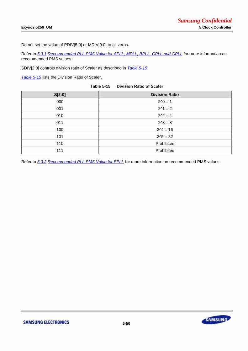
Samsung Confidential Exynos 5250_UM 5 Clock Controller
5-50
Do not set the value of PDIV[5:0] or MDIV[9:0] to all zeros.
Refer to 5.3.1 Recommended PLL PMS Value for APLL, MPLL, BPLL, CPLL and GPLL for more information on
recommended PMS values.
SDIV[2:0] controls division ratio of Scaler as described in Table 5-15.
Table 5-15 lists the Division Ratio of Scaler.
Table 5-15 Division Ratio of Scaler
S[2:0] Division Ratio
000 2^0 = 1
001 2^1 = 2
010 2^2 = 4
011 2^3 = 8
100 2^4 = 16
101 2^5 = 32
110 Prohibited
111 Prohibited
Refer to 5.3.2 Recommended PLL PMS Value for EPLL for more information on recommended PMS values.
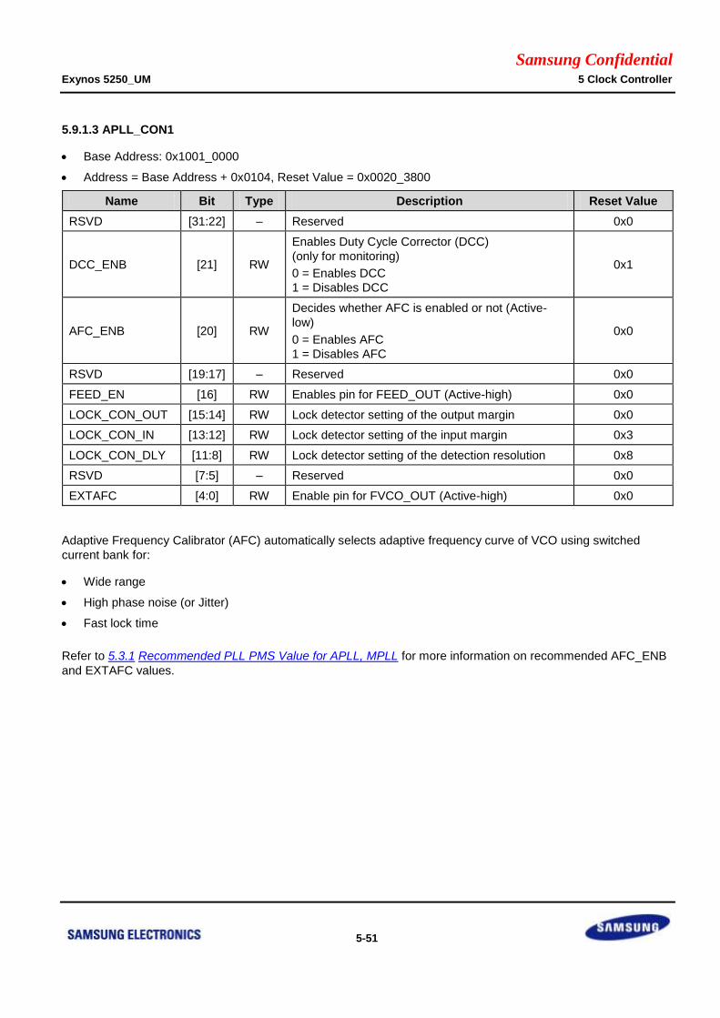
Samsung Confidential Exynos 5250_UM 5 Clock Controller
5-51
5.9.1.3 APLL_CON1
Base Address: 0x1001_0000
Address = Base Address + 0x0104, Reset Value = 0x0020_3800
Name Bit Type Description Reset Value
RSVD [31:22] – Reserved 0x0
DCC_ENB [21] RW
Enables Duty Cycle Corrector (DCC)
(only for monitoring)
0 = Enables DCC
1 = Disables DCC
0x1
AFC_ENB [20] RW
Decides whether AFC is enabled or not (Active-
low)
0 = Enables AFC
1 = Disables AFC
0x0
RSVD [19:17] – Reserved 0x0
FEED_EN [16] RW Enables pin for FEED_OUT (Active-high) 0x0
LOCK_CON_OUT [15:14] RW Lock detector setting of the output margin 0x0
LOCK_CON_IN [13:12] RW Lock detector setting of the input margin 0x3
LOCK_CON_DLY [11:8] RW Lock detector setting of the detection resolution 0x8
RSVD [7:5] – Reserved 0x0
EXTAFC [4:0] RW Enable pin for FVCO_OUT (Active-high) 0x0
Adaptive Frequency Calibrator (AFC) automatically selects adaptive frequency curve of VCO using switched
current bank for:
Wide range
High phase noise (or Jitter)
Fast lock time
Refer to 5.3.1 Recommended PLL PMS Value for APLL, MPLL for more information on recommended AFC_ENB
and EXTAFC values.
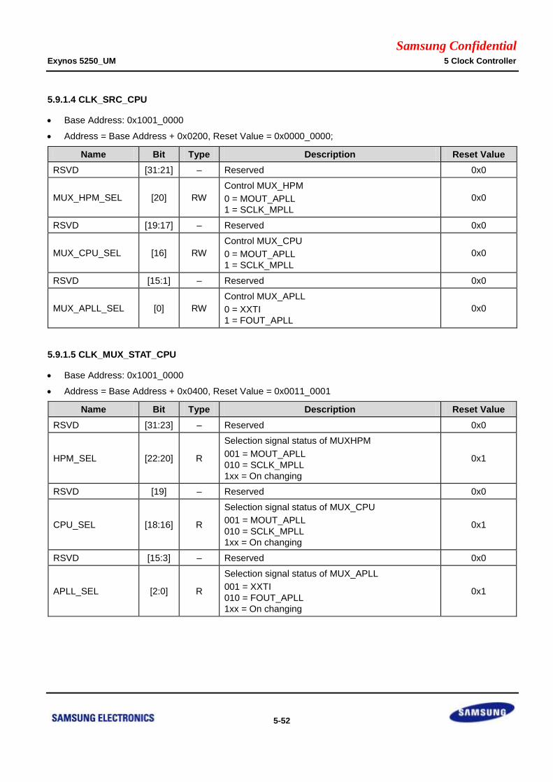
Samsung Confidential Exynos 5250_UM 5 Clock Controller
5-52
5.9.1.4 CLK_SRC_CPU
Base Address: 0x1001_0000
Address = Base Address + 0x0200, Reset Value = 0x0000_0000;
Name Bit Type Description Reset Value
RSVD [31:21] – Reserved 0x0
MUX_HPM_SEL [20] RW
Control MUX_HPM
0 = MOUT_APLL
1 = SCLK_MPLL
0x0
RSVD [19:17] – Reserved 0x0
MUX_CPU_SEL [16] RW
Control MUX_CPU
0 = MOUT_APLL
1 = SCLK_MPLL
0x0
RSVD [15:1] – Reserved 0x0
MUX_APLL_SEL [0] RW
Control MUX_APLL
0 = XXTI
1 = FOUT_APLL
0x0
5.9.1.5 CLK_MUX_STAT_CPU
Base Address: 0x1001_0000
Address = Base Address + 0x0400, Reset Value = 0x0011_0001
Name Bit Type Description Reset Value
RSVD [31:23] – Reserved 0x0
HPM_SEL [22:20] R
Selection signal status of MUXHPM
001 = MOUT_APLL
010 = SCLK_MPLL
1xx = On changing
0x1
RSVD [19] – Reserved 0x0
CPU_SEL [18:16] R
Selection signal status of MUX_CPU
001 = MOUT_APLL
010 = SCLK_MPLL
1xx = On changing
0x1
RSVD [15:3] – Reserved 0x0
APLL_SEL [2:0] R
Selection signal status of MUX_APLL
001 = XXTI
010 = FOUT_APLL
1xx = On changing
0x1
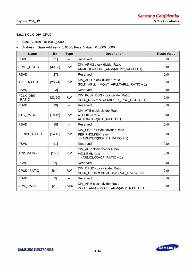
Samsung Confidential Exynos 5250_UM 5 Clock Controller
5-53
5.9.1.6 CLK_DIV_CPU0
Base Address: 0x1001_0000
Address = Base Address + 0x0500, Reset Value = 0x0000_0000
Name Bit Type Description Reset Value
RSVD [31] – Reserved 0x0
ARM2_RATIO [30:28] RW DIV_ARM2 clock divider Ratio
ARMCLK = DOUT_ARM/(ARM2_RATIO + 1) 0x0
RSVD [27] – Reserved 0x0
APLL_RATIO [26:24] RW DIV_APLL clock divider Ratio
SCLK_APLL = MOUT_APLL/(APLL_RATIO + 1) 0x0
RSVD [23] – Reserved 0x0
PCLK_DBG
_RATIO [22:20] RW
DIV_PCLK_DBG clock divider Ratio
PCLK_DBG = ATCLK/(PCLK_DBG_RATIO + 1) 0x0
RSVD [19] – Reserved 0x0
ATB_RATIO [18:16] RW
DIV_ATB clock divider Ratio
ATCLKEN ratio
=> ARMCLK/(ATB_RATIO + 1)
0x0
RSVD [15] – Reserved 0x0
PERIPH_RATIO [14:12] RW
DIV_PERIPH clock divider Ratio
PERIPHCLKEN ratio
=> ARMCLK/(PERIPH_RATIO + 1)
0x0
RSVD [11] – Reserved 0x0
ACP_RATIO [10:8] RW
DIV_ACP clock divider Ratio
ACLKENS ratio
=> ARMCLK/(ACP_RATIO + 1)
0x0
RSVD [7] – Reserved 0x0
CPUD_RATIO [6:4] RW DIV_CPUD clock divider Ratio
ACLK_CPUD = ARMCLK/(CPUD_RATIO + 1) 0x0
RSVD [3] – Reserved 0x0
ARM_RATIO [2:0] RWX DIV_ARM clock divider Ratio
DOUT_ARM = MOUT_ARM/(ARM_RATIO + 1) 0x0
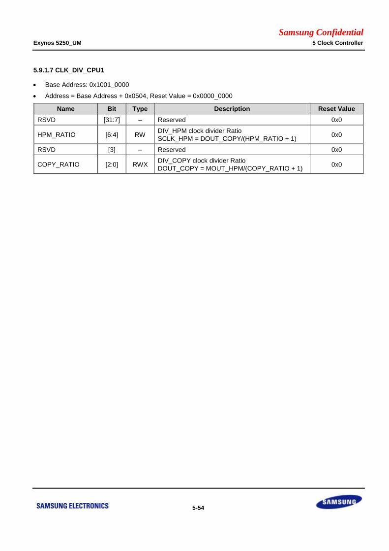
Samsung Confidential Exynos 5250_UM 5 Clock Controller
5-54
5.9.1.7 CLK_DIV_CPU1
Base Address: 0x1001_0000
Address = Base Address + 0x0504, Reset Value = 0x0000_0000
Name Bit Type Description Reset Value
RSVD [31:7] – Reserved 0x0
HPM_RATIO [6:4] RW DIV_HPM clock divider Ratio
SCLK_HPM = DOUT_COPY/(HPM_RATIO + 1) 0x0
RSVD [3] – Reserved 0x0
COPY_RATIO [2:0] RWX DIV_COPY clock divider Ratio
DOUT_COPY = MOUT_HPM/(COPY_RATIO + 1) 0x0
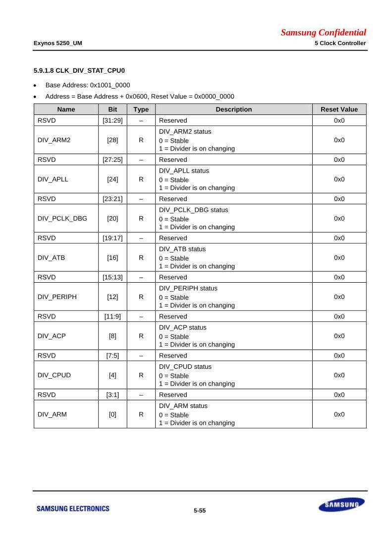
Samsung Confidential Exynos 5250_UM 5 Clock Controller
5-55
5.9.1.8 CLK_DIV_STAT_CPU0
Base Address: 0x1001_0000
Address = Base Address + 0x0600, Reset Value = 0x0000_0000
Name Bit Type Description Reset Value
RSVD [31:29] – Reserved 0x0
DIV_ARM2 [28] R
DIV_ARM2 status
0 = Stable
1 = Divider is on changing
0x0
RSVD [27:25] – Reserved 0x0
DIV_APLL [24] R
DIV_APLL status
0 = Stable
1 = Divider is on changing
0x0
RSVD [23:21] – Reserved 0x0
DIV_PCLK_DBG [20] R
DIV_PCLK_DBG status
0 = Stable
1 = Divider is on changing
0x0
RSVD [19:17] – Reserved 0x0
DIV_ATB [16] R
DIV_ATB status
0 = Stable
1 = Divider is on changing
0x0
RSVD [15:13] – Reserved 0x0
DIV_PERIPH [12] R
DIV_PERIPH status
0 = Stable
1 = Divider is on changing
0x0
RSVD [11:9] – Reserved 0x0
DIV_ACP [8] R
DIV_ACP status
0 = Stable
1 = Divider is on changing
0x0
RSVD [7:5] – Reserved 0x0
DIV_CPUD [4] R
DIV_CPUD status
0 = Stable
1 = Divider is on changing
0x0
RSVD [3:1] – Reserved 0x0
DIV_ARM [0] R
DIV_ARM status
0 = Stable
1 = Divider is on changing
0x0

Samsung Confidential Exynos 5250_UM 5 Clock Controller
5-56
5.9.1.9 CLK_DIV_STAT_CPU1
Base Address: 0x1001_0000
Address = 0x1004_4604, Reset Value = 0x0000_0000
Name Bit Type Description Reset Value
RSVD [31:5] – Reserved 0x0
DIV_HPM [4] R
DIV_HPM status
0 = Stable
1 = Divider is on changing
0x0
RSVD [3:1] – Reserved 0x0
DIV_COPY [0] R
DIV_COPY status
0 = Stable
1 = Divider is on changing
0x0
5.9.1.10 CLK_GATE_SCLK_CPU
Base Address: 0x1001_0000
Address = Base Address + 0x0800, Reset Value = 0xFFFF_FFFF
Name Bit Type Description Reset Value
RSVD [31:2] – Reserved 0x3FFF_FFFF
SCLK_HPM [1] RW
Gating Special Clock for HPM local clock
0 = Masks
1 = Passes
0x1
RSVD [0] – Reserved 0x1
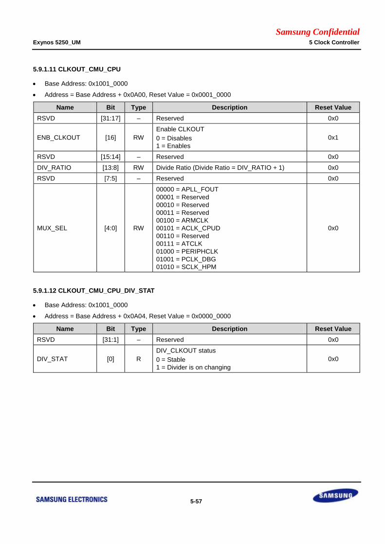
Samsung Confidential Exynos 5250_UM 5 Clock Controller
5-57
5.9.1.11 CLKOUT_CMU_CPU
Base Address: 0x1001_0000
Address = Base Address + 0x0A00, Reset Value = 0x0001_0000
Name Bit Type Description Reset Value
RSVD [31:17] – Reserved 0x0
ENB_CLKOUT [16] RW
Enable CLKOUT
0 = Disables
1 = Enables
0x1
RSVD [15:14] – Reserved 0x0
DIV_RATIO [13:8] RW Divide Ratio (Divide Ratio = DIV_RATIO + 1) 0x0
RSVD [7:5] – Reserved 0x0
MUX_SEL [4:0] RW
00000 = APLL_FOUT
00001 = Reserved
00010 = Reserved
00011 = Reserved
00100 = ARMCLK
00101 = ACLK_CPUD
00110 = Reserved
00111 = ATCLK
01000 = PERIPHCLK
01001 = PCLK_DBG
01010 = SCLK_HPM
0x0
5.9.1.12 CLKOUT_CMU_CPU_DIV_STAT
Base Address: 0x1001_0000
Address = Base Address + 0x0A04, Reset Value = 0x0000_0000
Name Bit Type Description Reset Value
RSVD [31:1] – Reserved 0x0
DIV_STAT [0] R
DIV_CLKOUT status
0 = Stable
1 = Divider is on changing
0x0
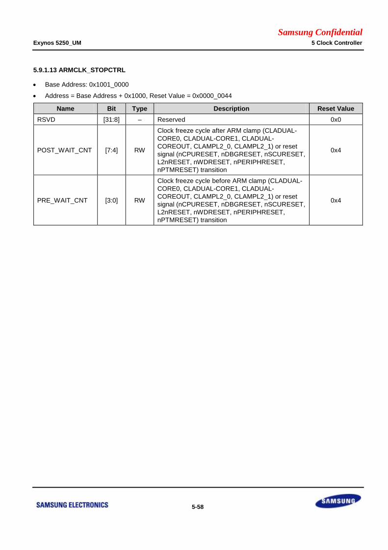
Samsung Confidential Exynos 5250_UM 5 Clock Controller
5-58
5.9.1.13 ARMCLK_STOPCTRL
Base Address: 0x1001_0000
Address = Base Address + 0x1000, Reset Value = 0x0000_0044
Name Bit Type Description Reset Value
RSVD [31:8] – Reserved 0x0
POST_WAIT_CNT [7:4] RW
Clock freeze cycle after ARM clamp (CLADUAL-
CORE0, CLADUAL-CORE1, CLADUAL-
COREOUT, CLAMPL2_0, CLAMPL2_1) or reset
signal (nCPURESET, nDBGRESET, nSCURESET,
L2nRESET, nWDRESET, nPERIPHRESET,
nPTMRESET) transition
0x4
PRE_WAIT_CNT [3:0] RW
Clock freeze cycle before ARM clamp (CLADUAL-
CORE0, CLADUAL-CORE1, CLADUAL-
COREOUT, CLAMPL2_0, CLAMPL2_1) or reset
signal (nCPURESET, nDBGRESET, nSCURESET,
L2nRESET, nWDRESET, nPERIPHRESET,
nPTMRESET) transition
0x4
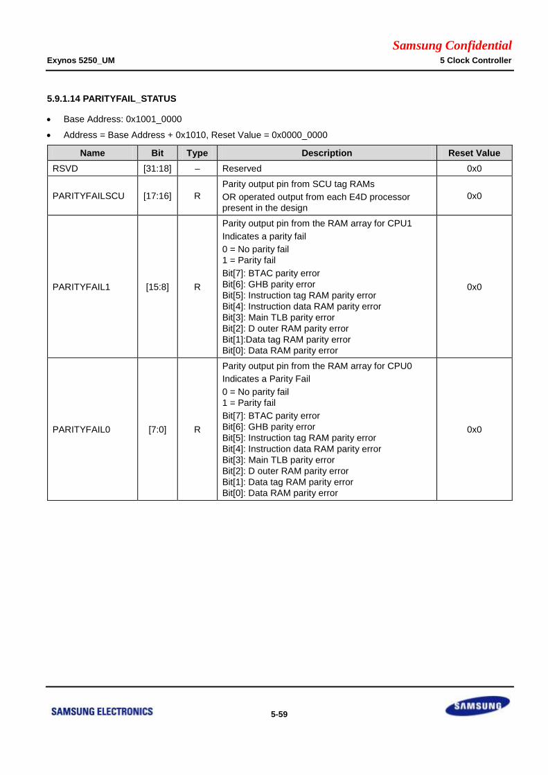
Samsung Confidential Exynos 5250_UM 5 Clock Controller
5-59
5.9.1.14 PARITYFAIL_STATUS
Base Address: 0x1001_0000
Address = Base Address + 0x1010, Reset Value = 0x0000_0000
Name Bit Type Description Reset Value
RSVD [31:18] – Reserved 0x0
PARITYFAILSCU [17:16] R
Parity output pin from SCU tag RAMs
OR operated output from each E4D processor
present in the design
0x0
PARITYFAIL1 [15:8] R
Parity output pin from the RAM array for CPU1
Indicates a parity fail
0 = No parity fail
1 = Parity fail
Bit[7]: BTAC parity error
Bit[6]: GHB parity error
Bit[5]: Instruction tag RAM parity error
Bit[4]: Instruction data RAM parity error
Bit[3]: Main TLB parity error
Bit[2]: D outer RAM parity error
Bit[1]:Data tag RAM parity error
Bit[0]: Data RAM parity error
0x0
PARITYFAIL0 [7:0] R
Parity output pin from the RAM array for CPU0
Indicates a Parity Fail
0 = No parity fail
1 = Parity fail
Bit[7]: BTAC parity error
Bit[6]: GHB parity error
Bit[5]: Instruction tag RAM parity error
Bit[4]: Instruction data RAM parity error
Bit[3]: Main TLB parity error
Bit[2]: D outer RAM parity error
Bit[1]: Data tag RAM parity error
Bit[0]: Data RAM parity error
0x0

Samsung Confidential Exynos 5250_UM 5 Clock Controller
5-60
5.9.1.15 PARITYFAIL_CLEAR
Base Address: 0x1001_0000
Address = Base Address + 0x1014, Reset Value = 0x0000_0000
Name Bit Type Description Reset Value
RSVD [31:18] – Reserved 0x0
PARITYFAILSCU [17:16] RWX
Parity output pin from SCU tag RAMs
OR operated output from each E4D processor
present in the design
0x0
PARITYFAIL1 [15:8] RWX
Parity output pin from the RAM array for CPU1
Indicates a Parity Fail
0 = No parity fail
1 = Parity fail
Bit[7]: BTAC parity error
Bit[6]: GHB parity error
Bit[5]: Instruction tag RAM parity error
Bit[4]: Instruction data RAM parity error
Bit[3]: Main TLB parity error
Bit[2]: D outer RAM parity error
Bit[1]: Data tag RAM parity error
Bit[0]: Data RAM parity error
0x0
PARITYFAIL0 [7:0] RWX
Parity output pin from the RAM array for CPU0
Indicates a parity fail
0 = No parity fail
1 = Parity fail
Bit[7]: BTAC parity error
Bit[6]: GHB parity error
Bit[5]: Instruction tag RAM parity error
Bit[4]: Instruction data RAM parity error
Bit[3]: Main TLB parity error
Bit[2]: D outer RAM parity error
Bit[1]: Data tag RAM parity error
Bit[0]: Data RAM parity error
0x0
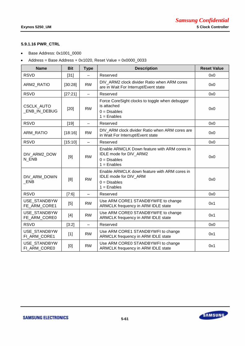
Samsung Confidential Exynos 5250_UM 5 Clock Controller
5-61
5.9.1.16 PWR_CTRL
Base Address: 0x1001_0000
Address = Base Address + 0x1020, Reset Value = 0x0000_0033
Name Bit Type Description Reset Value
RSVD [31] – Reserved 0x0
ARM2_RATIO [30:28] RW DIV_ARM2 clock divider Ratio when ARM cores
are in Wait For Interrupt/Event state 0x0
RSVD [27:21] – Reserved 0x0
CSCLK_AUTO
_ENB_IN_DEBUG [20] RW
Force CoreSight clocks to toggle when debugger
is attached
0 = Disables
1 = Enables
0x0
RSVD [19] – Reserved 0x0
ARM_RATIO [18:16] RW DIV_ARM clock divider Ratio when ARM cores are
in Wait For Interrupt/Event state 0x0
RSVD [15:10] – Reserved 0x0
DIV_ARM2_DOW
N_ENB [9] RW
Enable ARMCLK Down feature with ARM cores in
IDLE mode for DIV_ARM2
0 = Disables
1 = Enables
0x0
DIV_ARM_DOWN
_ENB [8] RW
Enable ARMCLK down feature with ARM cores in
IDLE mode for DIV_ARM
0 = Disables
1 = Enables
0x0
RSVD [7:6] – Reserved 0x0
USE_STANDBYW
FE_ARM_CORE1 [5] RW
Use ARM CORE1 STANDBYWFE to change
ARMCLK frequency in ARM IDLE state 0x1
USE_STANDBYW
FE_ARM_CORE0 [4] RW
Use ARM CORE0 STANDBYWFE to change
ARMCLK frequency in ARM IDLE state 0x1
RSVD [3:2] – Reserved 0x0
USE_STANDBYW
FI_ARM_CORE1 [1] RW
Use ARM CORE1 STANDBYWFI to change
ARMCLK frequency in ARM IDLE state 0x1
USE_STANDBYW
FI_ARM_CORE0 [0] RW
Use ARM CORE0 STANDBYWFI to change
ARMCLK frequency in ARM IDLE state 0x1
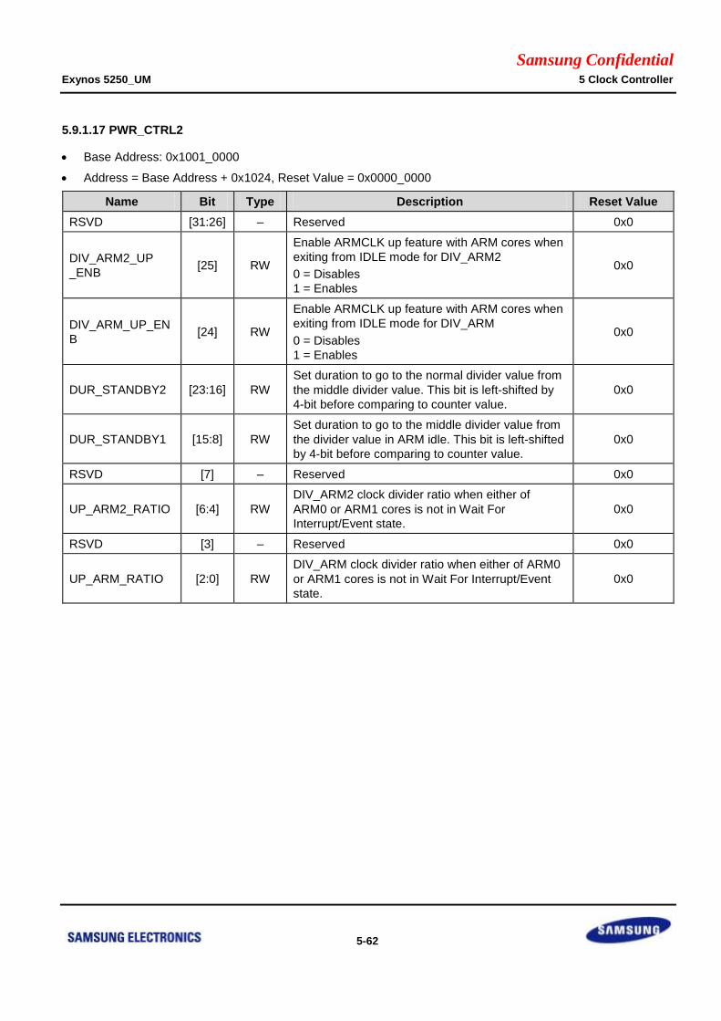
Samsung Confidential Exynos 5250_UM 5 Clock Controller
5-62
5.9.1.17 PWR_CTRL2
Base Address: 0x1001_0000
Address = Base Address + 0x1024, Reset Value = 0x0000_0000
Name Bit Type Description Reset Value
RSVD [31:26] – Reserved 0x0
DIV_ARM2_UP
_ENB [25] RW
Enable ARMCLK up feature with ARM cores when
exiting from IDLE mode for DIV_ARM2
0 = Disables
1 = Enables
0x0
DIV_ARM_UP_EN
B [24] RW
Enable ARMCLK up feature with ARM cores when
exiting from IDLE mode for DIV_ARM
0 = Disables
1 = Enables
0x0
DUR_STANDBY2 [23:16] RW
Set duration to go to the normal divider value from
the middle divider value. This bit is left-shifted by
4-bit before comparing to counter value.
0x0
DUR_STANDBY1 [15:8] RW
Set duration to go to the middle divider value from
the divider value in ARM idle. This bit is left-shifted
by 4-bit before comparing to counter value.
0x0
RSVD [7] – Reserved 0x0
UP_ARM2_RATIO [6:4] RW
DIV_ARM2 clock divider ratio when either of
ARM0 or ARM1 cores is not in Wait For
Interrupt/Event state.
0x0
RSVD [3] – Reserved 0x0
UP_ARM_RATIO [2:0] RW
DIV_ARM clock divider ratio when either of ARM0
or ARM1 cores is not in Wait For Interrupt/Event
state.
0x0
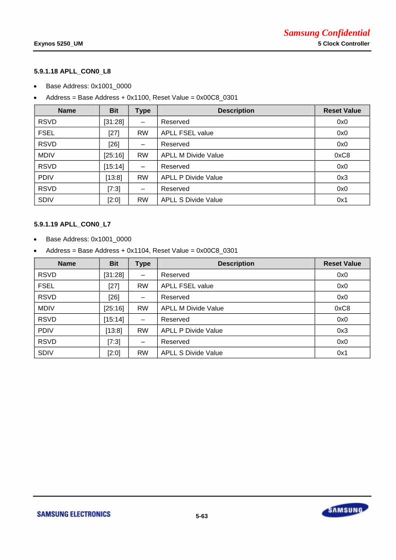
Samsung Confidential Exynos 5250_UM 5 Clock Controller
5-63
5.9.1.18 APLL_CON0_L8
Base Address: 0x1001_0000
Address = Base Address + 0x1100, Reset Value = 0x00C8_0301
Name Bit Type Description Reset Value
RSVD [31:28] – Reserved 0x0
FSEL [27] RW APLL FSEL value 0x0
RSVD [26] – Reserved 0x0
MDIV [25:16] RW APLL M Divide Value 0xC8
RSVD [15:14] – Reserved 0x0
PDIV [13:8] RW APLL P Divide Value 0x3
RSVD [7:3] – Reserved 0x0
SDIV [2:0] RW APLL S Divide Value 0x1
5.9.1.19 APLL_CON0_L7
Base Address: 0x1001_0000
Address = Base Address + 0x1104, Reset Value = 0x00C8_0301
Name Bit Type Description Reset Value
RSVD [31:28] – Reserved 0x0
FSEL [27] RW APLL FSEL value 0x0
RSVD [26] – Reserved 0x0
MDIV [25:16] RW APLL M Divide Value 0xC8
RSVD [15:14] – Reserved 0x0
PDIV [13:8] RW APLL P Divide Value 0x3
RSVD [7:3] – Reserved 0x0
SDIV [2:0] RW APLL S Divide Value 0x1

Samsung Confidential Exynos 5250_UM 5 Clock Controller
5-64
5.9.1.20 APLL_CON0_L6
Base Address: 0x1001_0000
Address = Base Address + 0x1108, Reset Value = 0x00C8_0301
Name Bit Type Description Reset Value
RSVD [31:28] – Reserved 0x0
FSEL [27] RW APLL FSEL value 0x0
RSVD [26] – Reserved 0x0
MDIV [25:16] RW APLL M Divide Value 0xC8
RSVD [15:14] – Reserved 0x0
PDIV [13:8] RW APLL P Divide Value 0x3
RSVD [7:3] – Reserved 0x0
SDIV [2:0] RW APLL S Divide Value 0x1
5.9.1.21 APLL_CON0_L5
Base Address: 0x1001_0000
Address = Base Address + 0x110C, Reset Value = 0x00C8_0301
Name Bit Type Description Reset Value
RSVD [31:28] – Reserved 0x0
FSEL [27] RW APLL FSEL value 0x0
RSVD [26] – Reserved 0x0
MDIV [25:16] RW APLL M Divide Value 0xC8
RSVD [15:14] – Reserved 0x0
PDIV [13:8] RW APLL P Divide Value 0x3
RSVD [7:3] – Reserved 0x0
SDIV [2:0] RW APLL S Divide Value 0x1

Samsung Confidential Exynos 5250_UM 5 Clock Controller
5-65
5.9.1.22 APLL_CON0_L4
Base Address: 0x1001_0000
Address = Base Address + 0x1110, Reset Value = 0x00C8_0301
Name Bit Type Description Reset Value
RSVD [31:28] – Reserved 0x0
FSEL [27] RW APLL FSEL value 0x0
RSVD [26] – Reserved 0x0
MDIV [25:16] RW APLL M Divide Value 0xC8
RSVD [15:14] – Reserved 0x0
PDIV [13:8] RW APLL P Divide Value 0x3
RSVD [7:3] – Reserved 0x0
SDIV [2:0] RW APLL S Divide Value 0x1
5.9.1.23 APLL_CON0_L3
Base Address: 0x1001_0000
Address = Base Address + 0x1114, Reset Value = 0x00C8_0301
Name Bit Type Description Reset Value
RSVD [31:28] – Reserved 0x0
FSEL [27] RW APLL FSEL value 0x0
RSVD [26] – Reserved 0x0
MDIV [25:16] RW APLL M Divide Value 0xC8
RSVD [15:14] – Reserved 0x0
PDIV [13:8] RW APLL P Divide Value 0x3
RSVD [7:3] – Reserved 0x0
SDIV [2:0] RW APLL S Divide Value 0x1

Samsung Confidential Exynos 5250_UM 5 Clock Controller
5-66
5.9.1.24 APLL_CON0_L2
Base Address: 0x1001_0000
Address = Base Address + 0x1118, Reset Value = 0x00C8_0301
Name Bit Type Description Reset Value
RSVD [31:28] – Reserved 0x0
FSEL [27] RW APLL FSEL value 0x0
RSVD [26] – Reserved 0x0
MDIV [25:16] RW APLL M Divide Value 0xC8
RSVD [15:14] – Reserved 0x0
PDIV [13:8] RW APLL P Divide Value 0x3
RSVD [7:3] – Reserved 0x0
SDIV [2:0] RW APLL S Divide Value 0x1
5.9.1.25 APLL_CON0_L1
Base Address: 0x1001_0000
Address = Base Address + 0x111C, Reset Value = 0x00C8_0301
Name Bit Type Description Reset Value
RSVD [31:28] – Reserved 0x0
FSEL [27] RW APLL FSEL value 0x0
RSVD [26] – Reserved 0x0
MDIV [25:16] RW APLL M Divide Value 0xC8
RSVD [15:14] – Reserved 0x0
PDIV [13:8] RW APLL P Divide Value 0x3
RSVD [7:3] – Reserved 0x0
SDIV [2:0] RW APLL S Divide Value 0x1
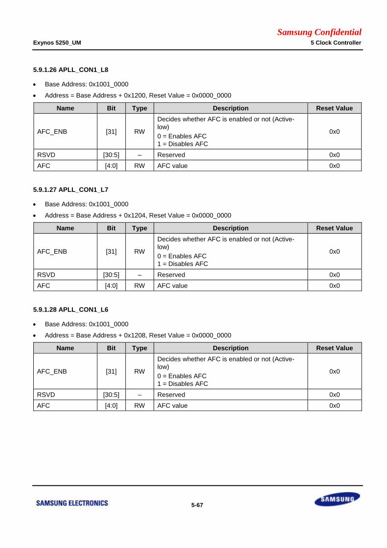
Samsung Confidential Exynos 5250_UM 5 Clock Controller
5-67
5.9.1.26 APLL_CON1_L8
Base Address: 0x1001_0000
Address = Base Address + 0x1200, Reset Value = 0x0000_0000
Name Bit Type Description Reset Value
AFC_ENB [31] RW
Decides whether AFC is enabled or not (Active-
low)
0 = Enables AFC
1 = Disables AFC
0x0
RSVD [30:5] – Reserved 0x0
AFC [4:0] RW AFC value 0x0
5.9.1.27 APLL_CON1_L7
Base Address: 0x1001_0000
Address = Base Address + 0x1204, Reset Value = 0x0000_0000
Name Bit Type Description Reset Value
AFC_ENB [31] RW
Decides whether AFC is enabled or not (Active-
low)
0 = Enables AFC
1 = Disables AFC
0x0
RSVD [30:5] – Reserved 0x0
AFC [4:0] RW AFC value 0x0
5.9.1.28 APLL_CON1_L6
Base Address: 0x1001_0000
Address = Base Address + 0x1208, Reset Value = 0x0000_0000
Name Bit Type Description Reset Value
AFC_ENB [31] RW
Decides whether AFC is enabled or not (Active-
low)
0 = Enables AFC
1 = Disables AFC
0x0
RSVD [30:5] – Reserved 0x0
AFC [4:0] RW AFC value 0x0
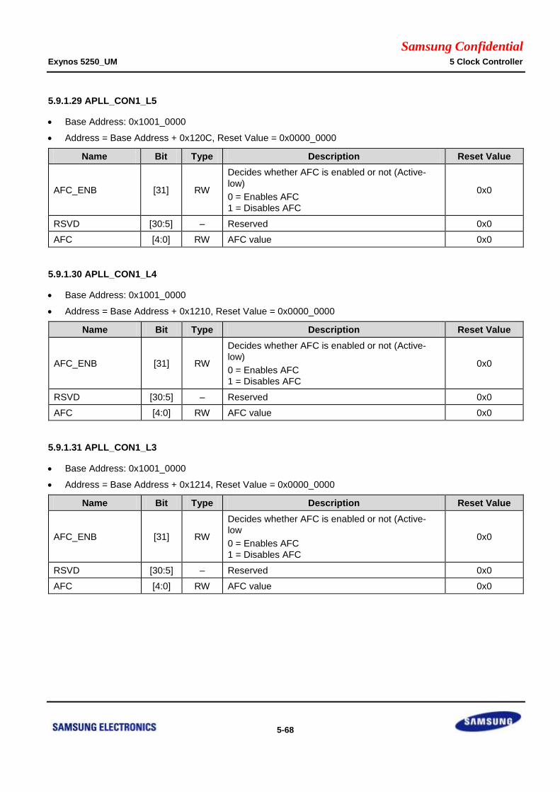
Samsung Confidential Exynos 5250_UM 5 Clock Controller
5-68
5.9.1.29 APLL_CON1_L5
Base Address: 0x1001_0000
Address = Base Address + 0x120C, Reset Value = 0x0000_0000
Name Bit Type Description Reset Value
AFC_ENB [31] RW
Decides whether AFC is enabled or not (Active-
low)
0 = Enables AFC
1 = Disables AFC
0x0
RSVD [30:5] – Reserved 0x0
AFC [4:0] RW AFC value 0x0
5.9.1.30 APLL_CON1_L4
Base Address: 0x1001_0000
Address = Base Address + 0x1210, Reset Value = 0x0000_0000
Name Bit Type Description Reset Value
AFC_ENB [31] RW
Decides whether AFC is enabled or not (Active-
low)
0 = Enables AFC
1 = Disables AFC
0x0
RSVD [30:5] – Reserved 0x0
AFC [4:0] RW AFC value 0x0
5.9.1.31 APLL_CON1_L3
Base Address: 0x1001_0000
Address = Base Address + 0x1214, Reset Value = 0x0000_0000
Name Bit Type Description Reset Value
AFC_ENB [31] RW
Decides whether AFC is enabled or not (Active-
low
0 = Enables AFC
1 = Disables AFC
0x0
RSVD [30:5] – Reserved 0x0
AFC [4:0] RW AFC value 0x0
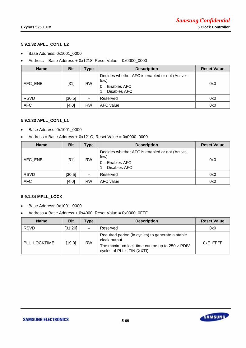
Samsung Confidential Exynos 5250_UM 5 Clock Controller
5-69
5.9.1.32 APLL_CON1_L2
Base Address: 0x1001_0000
Address = Base Address + 0x1218, Reset Value = 0x0000_0000
Name Bit Type Description Reset Value
AFC_ENB [31] RW
Decides whether AFC is enabled or not (Active-
low)
0 = Enables AFC
1 = Disables AFC
0x0
RSVD [30:5] – Reserved 0x0
AFC [4:0] RW AFC value 0x0
5.9.1.33 APLL_CON1_L1
Base Address: 0x1001_0000
Address = Base Address + 0x121C, Reset Value = 0x0000_0000
Name Bit Type Description Reset Value
AFC_ENB [31] RW
Decides whether AFC is enabled or not (Active-
low)
0 = Enables AFC
1 = Disables AFC
0x0
RSVD [30:5] – Reserved 0x0
AFC [4:0] RW AFC value 0x0
5.9.1.34 MPLL_LOCK
Base Address: 0x1001_0000
Address = Base Address + 0x4000, Reset Value = 0x0000_0FFF
Name Bit Type Description Reset Value
RSVD [31:20] – Reserved 0x0
PLL_LOCKTIME [19:0] RW
Required period (in cycles) to generate a stable
clock output
The maximum lock time can be up to 250 PDIV
cycles of PLL's FIN (XXTI).
0xF_FFFF
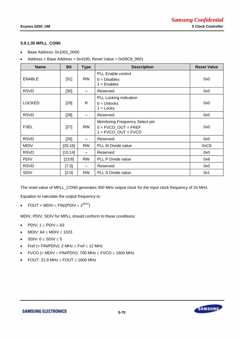
Samsung Confidential Exynos 5250_UM 5 Clock Controller
5-70
5.9.1.35 MPLL_CON0
Base Address: 0x1001_0000
Address = Base Address + 0x4100, Reset Value = 0x00C8_0601
Name Bit Type Description Reset Value
ENABLE [31] RW
PLL Enable control
0 = Disables
1 = Enables
0x0
RSVD [30] – Reserved 0x0
LOCKED [29] R
PLL Locking indication
0 = Unlocks
1 = Locks
0x0
RSVD [28] – Reserved 0x0
FSEL [27] RW
Monitoring Frequency Select pin
0 = FVCO_OUT = FREF
1 = FVCO_OUT = FVCO
0x0
RSVD [26] – Reserved 0x0
MDIV [25:16] RW PLL M Divide value 0xC8
RSVD [15:14] – Reserved 0x0
PDIV [13:8] RW PLL P Divide value 0x6
RSVD [7:3] – Reserved 0x0
SDIV [2:0] RW PLL S Divide value 0x1
The reset value of MPLL_CON0 generates 400 MHz output clock for the input clock frequency of 24 MHz.
Equation to calculate the output frequency is:
FOUT = MDIV FIN/(PDIV 2SDIV
)
MDIV, PDIV, SDIV for MPLL should conform to these conditions:
PDIV: 1 PDIV 63
MDIV: 64 MDIV 1023
SDIV: 0 SDIV 5
Fref (= FIN/PDIV): 2 MHz Fref 12 MHz
FVCO (= MDIV FIN/PDIV): 700 MHz FVCO 1600 MHz
FOUT: 21.9 MHz FOUT 1600 MHz
Samsung Confidential Exynos 5250_UM 5 Clock Controller
5-71
Do not set the value of PDIV[5:0] or MDIV[9:0] to all zeros
Refer to 5.3.1 Recommended PLL PMS Value for APLL, MPLL for more information on recommended PMS
values.
SDIV[2:0] controls division ratio of Scaler as described in Table 5-15.

Samsung Confidential Exynos 5250_UM 5 Clock Controller
5-72
5.9.1.36 MPLL_CON1
Base Address: 0x1001_0000
Address = Base Address + 0x4104, Reset Value = 0x0020_3800
Name Bit Type Description Reset Value
RSVD [31:22] – Reserved 0x0
DCC_ENB [21] RW
Enables Duty Cycle Corrector
(only for monitoring)
0 = Enables DCC
1 = Disables DCC
0x1
AFC_ENB [20] RW
Decides whether AFC is enabled or not (Active-
low)
0 = Enables AFC
1 = Disables AFC
0x0
RSVD [19:17] – Reserved 0x0
FEED_EN [16] RW Enable pin for FEED_OUT (Active-high) 0x0
LOCK_CON_OUT [15:14] RW Lock detector setting of the output margin 0x0
LOCK_CON_IN [13:12] RW Lock detector setting of the input margin 0x3
LOCK_CON_DLY [11:8] RW Lock detector setting of the detection resolution 0x8
RSVD [7:5] – Reserved 0x0
EXTAFC [4:0] RW Enable pin for FVCO_OUT (Active-high) 0x0
AFC automatically selects adaptive frequency curve of VCO using switched current bank for:
Wide range
High phase noise (or Jitter)
Fast lock time
Refer to 5.3.1 Recommended PLL PMS Value for APLL, MPLL, BPLL, CPLL and GPLL for more information on
recommended AFC_ENB and EXTAFC values.
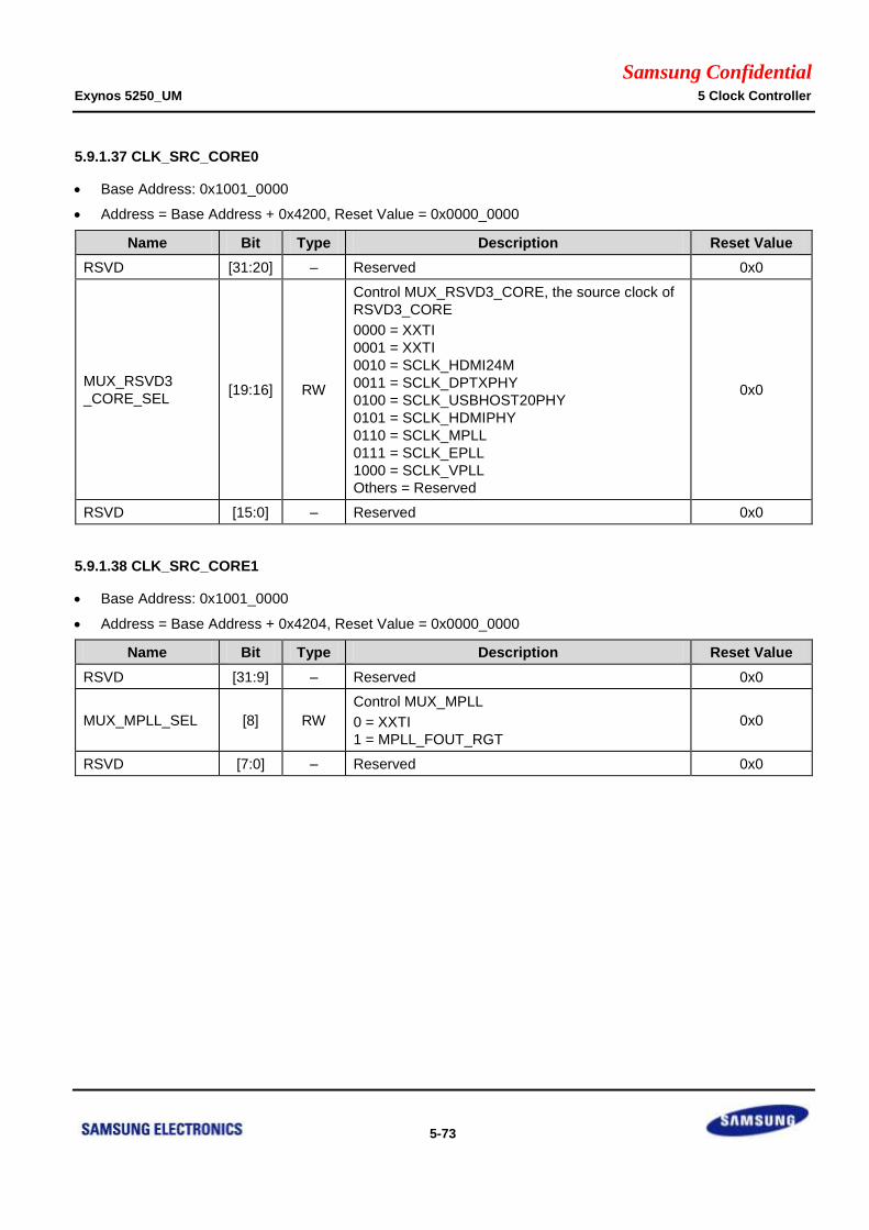
Samsung Confidential Exynos 5250_UM 5 Clock Controller
5-73
5.9.1.37 CLK_SRC_CORE0
Base Address: 0x1001_0000
Address = Base Address + 0x4200, Reset Value = 0x0000_0000
Name Bit Type Description Reset Value
RSVD [31:20] – Reserved 0x0
MUX_RSVD3
_CORE_SEL [19:16] RW
Control MUX_RSVD3_CORE, the source clock of
RSVD3_CORE
0000 = XXTI
0001 = XXTI
0010 = SCLK_HDMI24M
0011 = SCLK_DPTXPHY
0100 = SCLK_USBHOST20PHY
0101 = SCLK_HDMIPHY
0110 = SCLK_MPLL
0111 = SCLK_EPLL
1000 = SCLK_VPLL
Others = Reserved
0x0
RSVD [15:0] – Reserved 0x0
5.9.1.38 CLK_SRC_CORE1
Base Address: 0x1001_0000
Address = Base Address + 0x4204, Reset Value = 0x0000_0000
Name Bit Type Description Reset Value
RSVD [31:9] – Reserved 0x0
MUX_MPLL_SEL [8] RW
Control MUX_MPLL
0 = XXTI
1 = MPLL_FOUT_RGT
0x0
RSVD [7:0] – Reserved 0x0
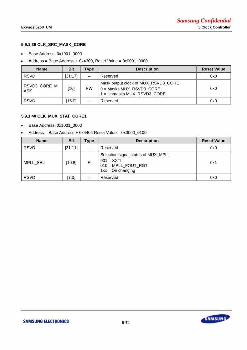
Samsung Confidential Exynos 5250_UM 5 Clock Controller
5-74
5.9.1.39 CLK_SRC_MASK_CORE
Base Address: 0x1001_0000
Address = Base Address + 0x4300, Reset Value = 0x0001_0000
Name Bit Type Description Reset Value
RSVD [31:17] – Reserved 0x0
RSVD3_CORE_M
ASK [16] RW
Mask output clock of MUX_RSVD3_CORE
0 = Masks MUX_RSVD3_CORE
1 = Unmasks MUX_RSVD3_CORE
0x0
RSVD [15:0] – Reserved 0x0
5.9.1.40 CLK_MUX_STAT_CORE1
Base Address: 0x1001_0000
Address = Base Address + 0x4404 Reset Value = 0x0000_0100
Name Bit Type Description Reset Value
RSVD [31:11] – Reserved 0x0
MPLL_SEL [10:8] R
Selection signal status of MUX_MPLL
001 = XXTI
010 = MPLL_FOUT_RGT
1xx = On changing
0x1
RSVD [7:0] – Reserved 0x0
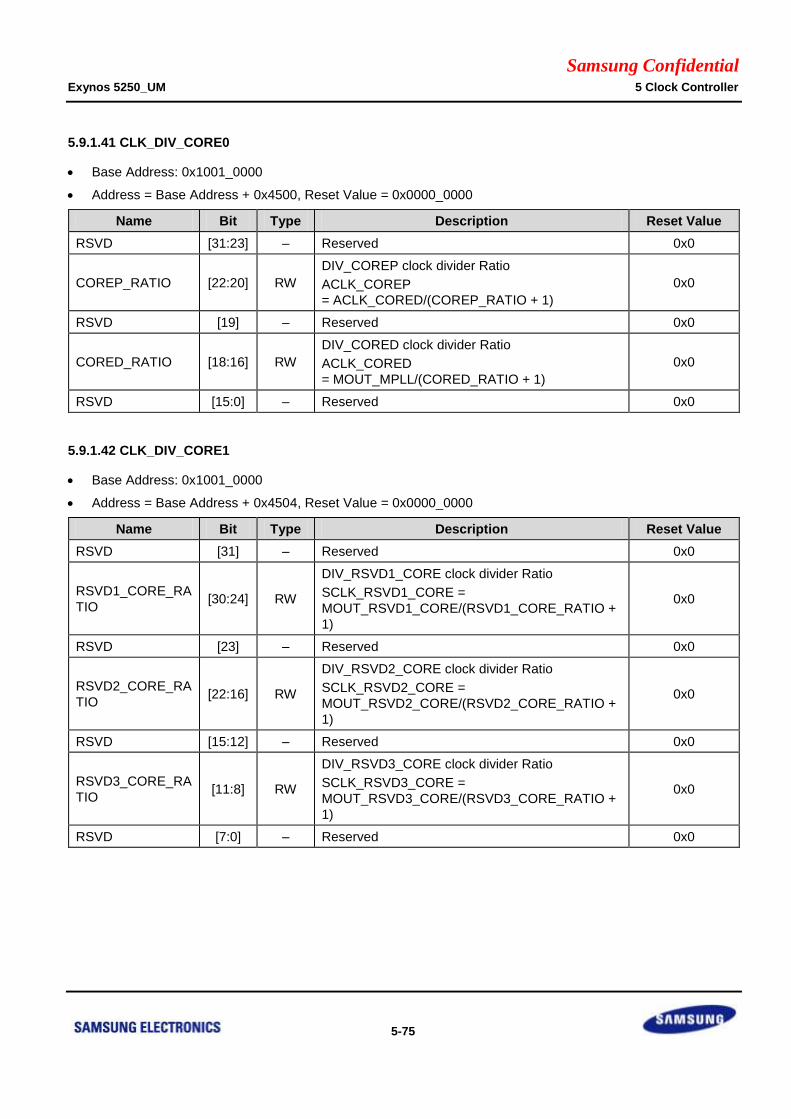
Samsung Confidential Exynos 5250_UM 5 Clock Controller
5-75
5.9.1.41 CLK_DIV_CORE0
Base Address: 0x1001_0000
Address = Base Address + 0x4500, Reset Value = 0x0000_0000
Name Bit Type Description Reset Value
RSVD [31:23] – Reserved 0x0
COREP_RATIO [22:20] RW
DIV_COREP clock divider Ratio
ACLK_COREP
= ACLK_CORED/(COREP_RATIO + 1)
0x0
RSVD [19] – Reserved 0x0
CORED_RATIO [18:16] RW
DIV_CORED clock divider Ratio
ACLK_CORED
= MOUT_MPLL/(CORED_RATIO + 1)
0x0
RSVD [15:0] – Reserved 0x0
5.9.1.42 CLK_DIV_CORE1
Base Address: 0x1001_0000
Address = Base Address + 0x4504, Reset Value = 0x0000_0000
Name Bit Type Description Reset Value
RSVD [31] – Reserved 0x0
RSVD1_CORE_RA
TIO [30:24] RW
DIV_RSVD1_CORE clock divider Ratio
SCLK_RSVD1_CORE =
MOUT_RSVD1_CORE/(RSVD1_CORE_RATIO +
1)
0x0
RSVD [23] – Reserved 0x0
RSVD2_CORE_RA
TIO [22:16] RW
DIV_RSVD2_CORE clock divider Ratio
SCLK_RSVD2_CORE =
MOUT_RSVD2_CORE/(RSVD2_CORE_RATIO +
1)
0x0
RSVD [15:12] – Reserved 0x0
RSVD3_CORE_RA
TIO [11:8] RW
DIV_RSVD3_CORE clock divider Ratio
SCLK_RSVD3_CORE =
MOUT_RSVD3_CORE/(RSVD3_CORE_RATIO +
1)
0x0
RSVD [7:0] – Reserved 0x0
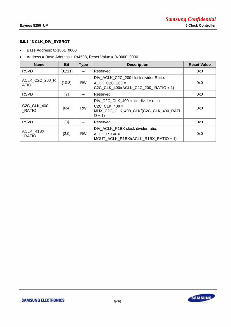
Samsung Confidential Exynos 5250_UM 5 Clock Controller
5-76
5.9.1.43 CLK_DIV_SYSRGT
Base Address: 0x1001_0000
Address = Base Address + 0x4508, Reset Value = 0x0000_0000
Name Bit Type Description Reset Value
RSVD [31:11] – Reserved 0x0
ACLK_C2C_200_R
ATIO [10:8] RW
DIV_ACLK_C2C_200 clock divider Ratio.
ACLK_C2C_200 =
C2C_CLK_400/(ACLK_C2C_200_ RATIO + 1)
0x0
RSVD [7] – Reserved 0x0
C2C_CLK_400
_RATIO [6:4] RW
DIV_C2C_CLK_400 clock divider ratio,
C2C_CLK_400 =
MUX_C2C_CLK_400_CLK/(C2C_CLK_400_RATI
O + 1)
0x0
RSVD [3] – Reserved 0x0
ACLK_R1BX
_RATIO [2:0] RW
DIV_ACLK_R1BX clock divider ratio,
ACLK_R1BX =
MOUT_ACLK_R1BX/(ACLK_R1BX_RATIO + 1)
0x0
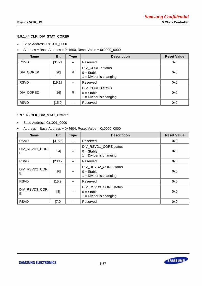
Samsung Confidential Exynos 5250_UM 5 Clock Controller
5-77
5.9.1.44 CLK_DIV_STAT_CORE0
Base Address: 0x1001_0000
Address = Base Address + 0x4600, Reset Value = 0x0000_0000
Name Bit Type Description Reset Value
RSVD [31:21] – Reserved 0x0
DIV_COREP [20] R
DIV_COREP status
0 = Stable
1 = Divider is changing
0x0
RSVD [19:17] – Reserved 0x0
DIV_CORED [16] R
DIV_CORED status
0 = Stable
1 = Divider is changing
0x0
RSVD [15:0] – Reserved 0x0
5.9.1.45 CLK_DIV_STAT_CORE1
Base Address: 0x1001_0000
Address = Base Address + 0x4604, Reset Value = 0x0000_0000
Name Bit Type Description Reset Value
RSVD [31:25] – Reserved 0x0
DIV_RSVD1_COR
E [24] –
DIV_RSVD1_CORE status
0 = Stable
1 = Divider is changing
0x0
RSVD [23:17] – Reserved 0x0
DIV_RSVD2_COR
E [16] –
DIV_RSVD2_CORE status
0 = Stable
1 = Divider is changing
0x0
RSVD [15:9] – Reserved 0x0
DIV_RSVD3_COR
E [8] –
DIV_RSVD3_CORE status
0 = Stable
1 = Divider is changing
0x0
RSVD [7:0] – Reserved 0x0
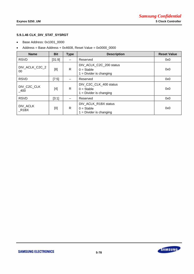
Samsung Confidential Exynos 5250_UM 5 Clock Controller
5-78
5.9.1.46 CLK_DIV_STAT_SYSRGT
Base Address: 0x1001_0000
Address = Base Address + 0x4608, Reset Value = 0x0000_0000
Name Bit Type Description Reset Value
RSVD [31:9] – Reserved 0x0
DIV_ACLK_C2C_2
00 [8] R
DIV_ACLK_C2C_200 status
0 = Stable
1 = Divider is changing
0x0
RSVD [7:5] – Reserved 0x0
DIV_C2C_CLK
_400 [4] R
DIV_C2C_CLK_400 status
0 = Stable
1 = Divider is changing
0x0
RSVD [3:1] – Reserved 0x0
DIV_ACLK
_R1BX [0] R
DIV_ACLK_R1BX status
0 = Stable
1 = Divider is changing
0x0
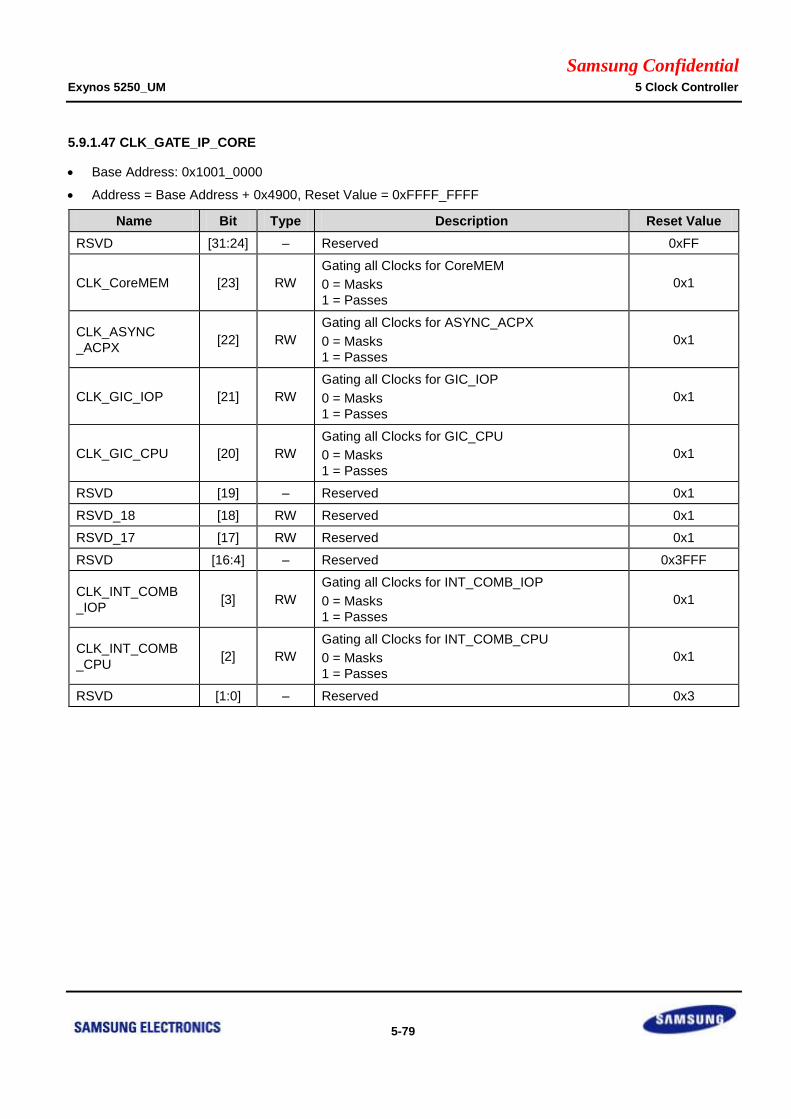
Samsung Confidential Exynos 5250_UM 5 Clock Controller
5-79
5.9.1.47 CLK_GATE_IP_CORE
Base Address: 0x1001_0000
Address = Base Address + 0x4900, Reset Value = 0xFFFF_FFFF
Name Bit Type Description Reset Value
RSVD [31:24] – Reserved 0xFF
CLK_CoreMEM [23] RW
Gating all Clocks for CoreMEM
0 = Masks
1 = Passes
0x1
CLK_ASYNC
_ACPX [22] RW
Gating all Clocks for ASYNC_ACPX
0 = Masks
1 = Passes
0x1
CLK_GIC_IOP [21] RW
Gating all Clocks for GIC_IOP
0 = Masks
1 = Passes
0x1
CLK_GIC_CPU [20] RW
Gating all Clocks for GIC_CPU
0 = Masks
1 = Passes
0x1
RSVD [19] – Reserved 0x1
RSVD_18 [18] RW Reserved 0x1
RSVD_17 [17] RW Reserved 0x1
RSVD [16:4] – Reserved 0x3FFF
CLK_INT_COMB
_IOP [3] RW
Gating all Clocks for INT_COMB_IOP
0 = Masks
1 = Passes
0x1
CLK_INT_COMB
_CPU [2] RW
Gating all Clocks for INT_COMB_CPU
0 = Masks
1 = Passes
0x1
RSVD [1:0] – Reserved 0x3
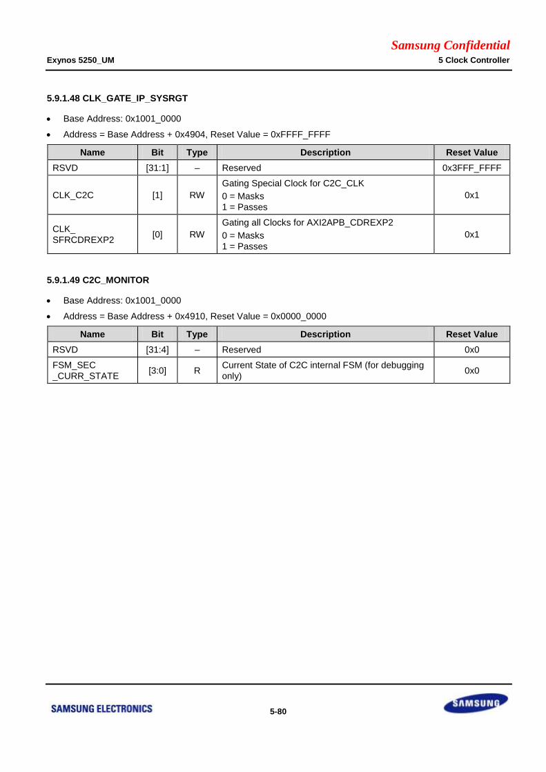
Samsung Confidential Exynos 5250_UM 5 Clock Controller
5-80
5.9.1.48 CLK_GATE_IP_SYSRGT
Base Address: 0x1001_0000
Address = Base Address + 0x4904, Reset Value = 0xFFFF_FFFF
Name Bit Type Description Reset Value
RSVD [31:1] – Reserved 0x3FFF_FFFF
CLK_C2C [1] RW
Gating Special Clock for C2C_CLK
0 = Masks
1 = Passes
0x1
CLK_
SFRCDREXP2 [0] RW
Gating all Clocks for AXI2APB_CDREXP2
0 = Masks
1 = Passes
0x1
5.9.1.49 C2C_MONITOR
Base Address: 0x1001_0000
Address = Base Address + 0x4910, Reset Value = 0x0000_0000
Name Bit Type Description Reset Value
RSVD [31:4] – Reserved 0x0
FSM_SEC
_CURR_STATE [3:0] R
Current State of C2C internal FSM (for debugging
only) 0x0
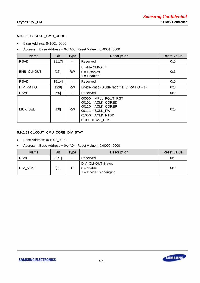
Samsung Confidential Exynos 5250_UM 5 Clock Controller
5-81
5.9.1.50 CLKOUT_CMU_CORE
Base Address: 0x1001_0000
Address = Base Address + 0x4A00, Reset Value = 0x0001_0000
Name Bit Type Description Reset Value
RSVD [31:17] – Reserved 0x0
ENB_CLKOUT [16] RW
Enable CLKOUT
0 = Disables
1 = Enables
0x1
RSVD [15:14] – Reserved 0x0
DIV_RATIO [13:8] RW Divide Ratio (Divide ratio = DIV_RATIO + 1) 0x0
RSVD [7:5] – Reserved 0x0
MUX_SEL [4:0] RW
00000 = MPLL_FOUT_RGT
00101 = ACLK_CORED
00110 = ACLK_COREP
00111 = SCLK_PWI
01000 = ACLK_R1BX
01001 = C2C_CLK
0x0
5.9.1.51 CLKOUT_CMU_CORE_DIV_STAT
Base Address: 0x1001_0000
Address = Base Address + 0x4A04, Reset Value = 0x0000_0000
Name Bit Type Description Reset Value
RSVD [31:1] – Reserved 0x0
DIV_STAT [0] R
DIV_CLKOUT Status
0 = Stable
1 = Divider is changing
0x0
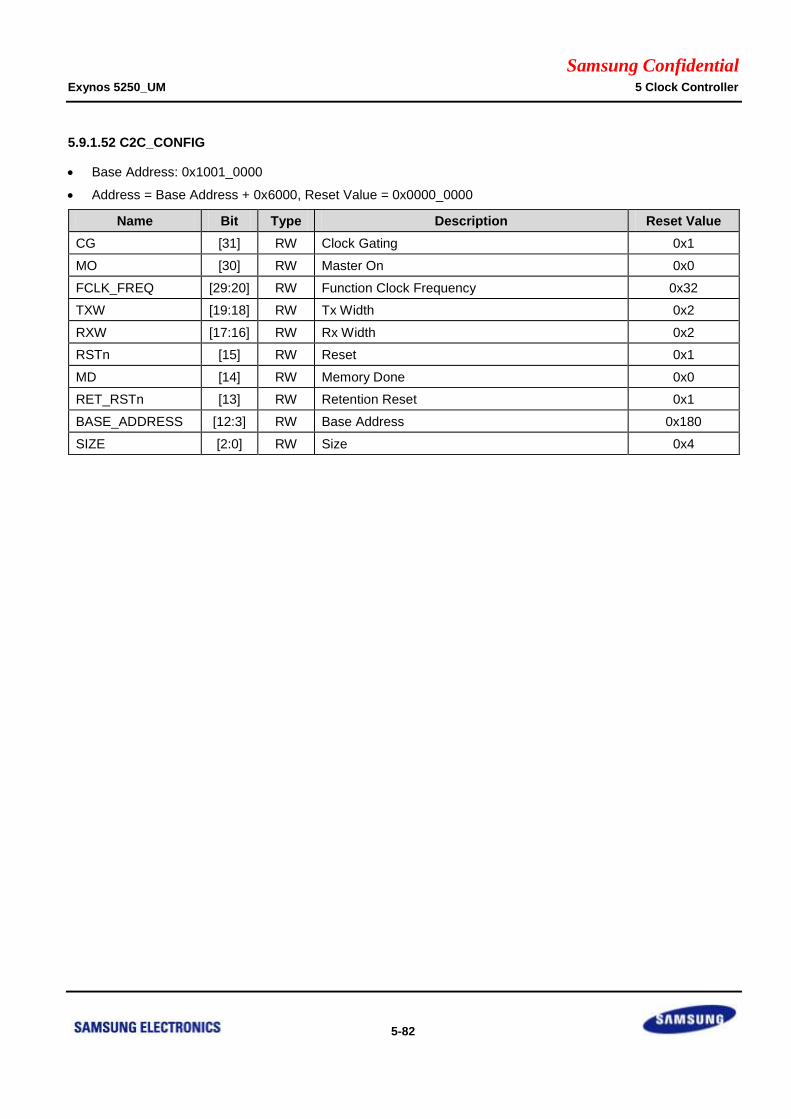
Samsung Confidential Exynos 5250_UM 5 Clock Controller
5-82
5.9.1.52 C2C_CONFIG
Base Address: 0x1001_0000
Address = Base Address + 0x6000, Reset Value = 0x0000_0000
Name Bit Type Description Reset Value
CG [31] RW Clock Gating 0x1
MO [30] RW Master On 0x0
FCLK_FREQ [29:20] RW Function Clock Frequency 0x32
TXW [19:18] RW Tx Width 0x2
RXW [17:16] RW Rx Width 0x2
RSTn [15] RW Reset 0x1
MD [14] RW Memory Done 0x0
RET_RSTn [13] RW Retention Reset 0x1
BASE_ADDRESS [12:3] RW Base Address 0x180
SIZE [2:0] RW Size 0x4
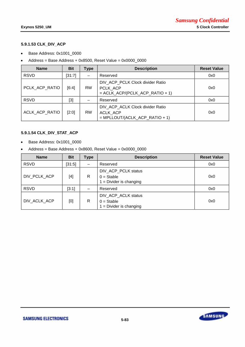
Samsung Confidential Exynos 5250_UM 5 Clock Controller
5-83
5.9.1.53 CLK_DIV_ACP
Base Address: 0x1001_0000
Address = Base Address + 0x8500, Reset Value = 0x0000_0000
Name Bit Type Description Reset Value
RSVD [31:7] – Reserved 0x0
PCLK_ACP_RATIO [6:4] RW
DIV_ACP_PCLK Clock divider Ratio
PCLK_ACP
= ACLK_ACP/(PCLK_ACP_RATIO + 1)
0x0
RSVD [3] – Reserved 0x0
ACLK_ACP_RATIO [2:0] RW
DIV_ACP_ACLK Clock divider Ratio
ACLK_ACP
= MPLLOUT/(ACLK_ACP_RATIO + 1)
0x0
5.9.1.54 CLK_DIV_STAT_ACP
Base Address: 0x1001_0000
Address = Base Address + 0x8600, Reset Value = 0x0000_0000
Name Bit Type Description Reset Value
RSVD [31:5] – Reserved 0x0
DIV_PCLK_ACP [4] R
DIV_ACP_PCLK status
0 = Stable
1 = Divider is changing
0x0
RSVD [3:1] – Reserved 0x0
DIV_ACLK_ACP [0] R
DIV_ACP_ACLK status
0 = Stable
1 = Divider is changing
0x0
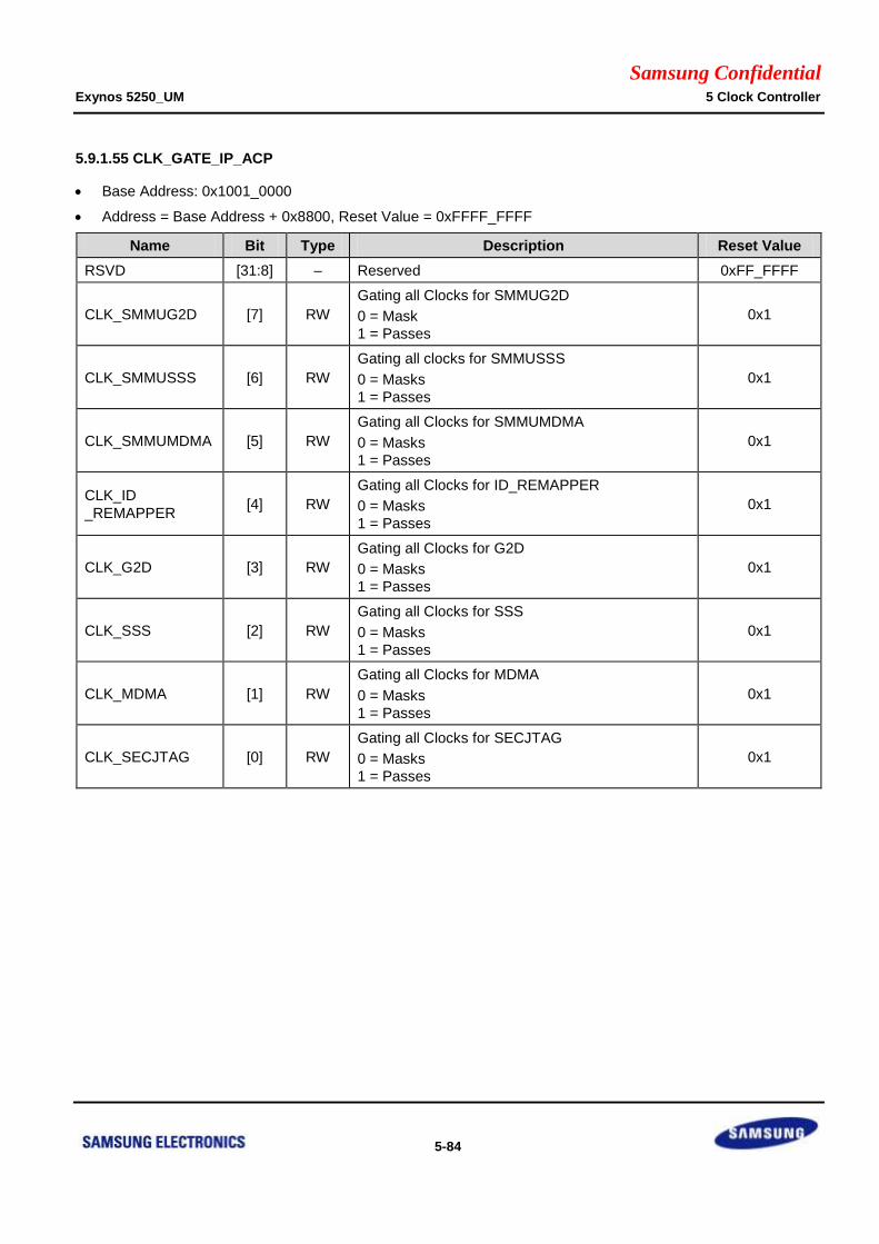
Samsung Confidential Exynos 5250_UM 5 Clock Controller
5-84
5.9.1.55 CLK_GATE_IP_ACP
Base Address: 0x1001_0000
Address = Base Address + 0x8800, Reset Value = 0xFFFF_FFFF
Name Bit Type Description Reset Value
RSVD [31:8] – Reserved 0xFF_FFFF
CLK_SMMUG2D [7] RW
Gating all Clocks for SMMUG2D
0 = Mask
1 = Passes
0x1
CLK_SMMUSSS [6] RW
Gating all clocks for SMMUSSS
0 = Masks
1 = Passes
0x1
CLK_SMMUMDMA [5] RW
Gating all Clocks for SMMUMDMA
0 = Masks
1 = Passes
0x1
CLK_ID
_REMAPPER [4] RW
Gating all Clocks for ID_REMAPPER
0 = Masks
1 = Passes
0x1
CLK_G2D [3] RW
Gating all Clocks for G2D
0 = Masks
1 = Passes
0x1
CLK_SSS [2] RW
Gating all Clocks for SSS
0 = Masks
1 = Passes
0x1
CLK_MDMA [1] RW
Gating all Clocks for MDMA
0 = Masks
1 = Passes
0x1
CLK_SECJTAG [0] RW
Gating all Clocks for SECJTAG
0 = Masks
1 = Passes
0x1
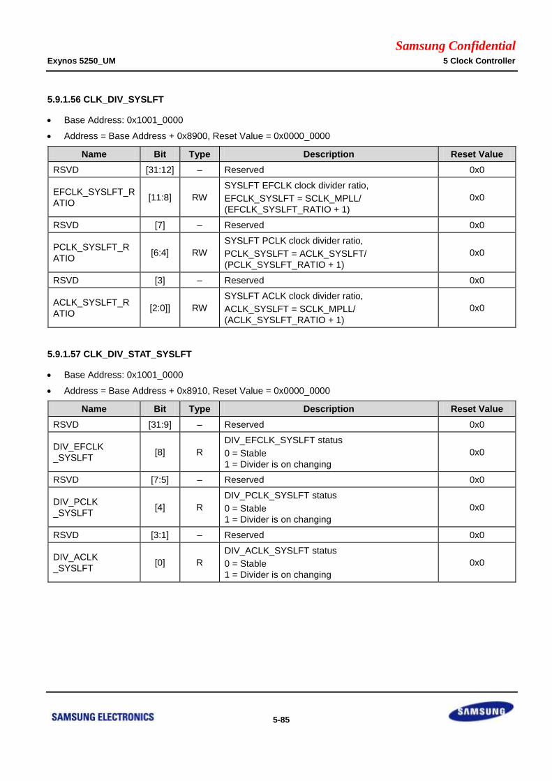
Samsung Confidential Exynos 5250_UM 5 Clock Controller
5-85
5.9.1.56 CLK_DIV_SYSLFT
Base Address: 0x1001_0000
Address = Base Address + 0x8900, Reset Value = 0x0000_0000
Name Bit Type Description Reset Value
RSVD [31:12] – Reserved 0x0
EFCLK_SYSLFT_R
ATIO [11:8] RW
SYSLFT EFCLK clock divider ratio,
EFCLK_SYSLFT = SCLK_MPLL/
(EFCLK_SYSLFT_RATIO + 1)
0x0
RSVD [7] – Reserved 0x0
PCLK_SYSLFT_R
ATIO [6:4] RW
SYSLFT PCLK clock divider ratio,
PCLK_SYSLFT = ACLK_SYSLFT/
(PCLK_SYSLFT_RATIO + 1)
0x0
RSVD [3] – Reserved 0x0
ACLK_SYSLFT_R
ATIO [2:0]] RW
SYSLFT ACLK clock divider ratio,
ACLK_SYSLFT = SCLK_MPLL/
(ACLK_SYSLFT_RATIO + 1)
0x0
5.9.1.57 CLK_DIV_STAT_SYSLFT
Base Address: 0x1001_0000
Address = Base Address + 0x8910, Reset Value = 0x0000_0000
Name Bit Type Description Reset Value
RSVD [31:9] – Reserved 0x0
DIV_EFCLK
_SYSLFT [8] R
DIV_EFCLK_SYSLFT status
0 = Stable
1 = Divider is on changing
0x0
RSVD [7:5] – Reserved 0x0
DIV_PCLK
_SYSLFT [4] R
DIV_PCLK_SYSLFT status
0 = Stable
1 = Divider is on changing
0x0
RSVD [3:1] – Reserved 0x0
DIV_ACLK
_SYSLFT [0] R
DIV_ACLK_SYSLFT status
0 = Stable
1 = Divider is on changing
0x0
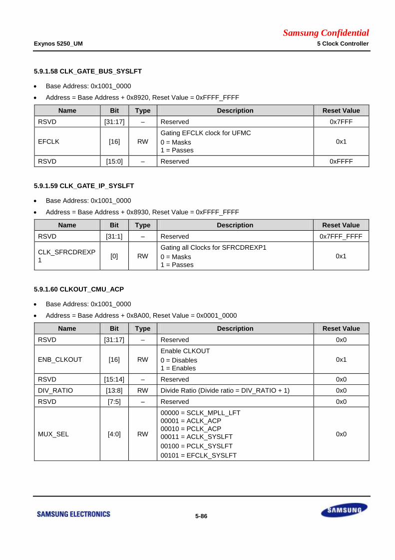
Samsung Confidential Exynos 5250_UM 5 Clock Controller
5-86
5.9.1.58 CLK_GATE_BUS_SYSLFT
Base Address: 0x1001_0000
Address = Base Address + 0x8920, Reset Value = 0xFFFF_FFFF
Name Bit Type Description Reset Value
RSVD [31:17] – Reserved 0x7FFF
EFCLK [16] RW
Gating EFCLK clock for UFMC
0 = Masks
1 = Passes
0x1
RSVD [15:0] – Reserved 0xFFFF
5.9.1.59 CLK_GATE_IP_SYSLFT
Base Address: 0x1001_0000
Address = Base Address + 0x8930, Reset Value = 0xFFFF_FFFF
Name Bit Type Description Reset Value
RSVD [31:1] – Reserved 0x7FFF_FFFF
CLK_SFRCDREXP
1 [0] RW
Gating all Clocks for SFRCDREXP1
0 = Masks
1 = Passes
0x1
5.9.1.60 CLKOUT_CMU_ACP
Base Address: 0x1001_0000
Address = Base Address + 0x8A00, Reset Value = 0x0001_0000
Name Bit Type Description Reset Value
RSVD [31:17] – Reserved 0x0
ENB_CLKOUT [16] RW
Enable CLKOUT
0 = Disables
1 = Enables
0x1
RSVD [15:14] – Reserved 0x0
DIV_RATIO [13:8] RW Divide Ratio (Divide ratio = DIV_RATIO + 1) 0x0
RSVD [7:5] – Reserved 0x0
MUX_SEL [4:0] RW
00000 = SCLK_MPLL_LFT
00001 = ACLK_ACP
00010 = PCLK_ACP
00011 = ACLK_SYSLFT
00100 = PCLK_SYSLFT
00101 = EFCLK_SYSLFT
0x0
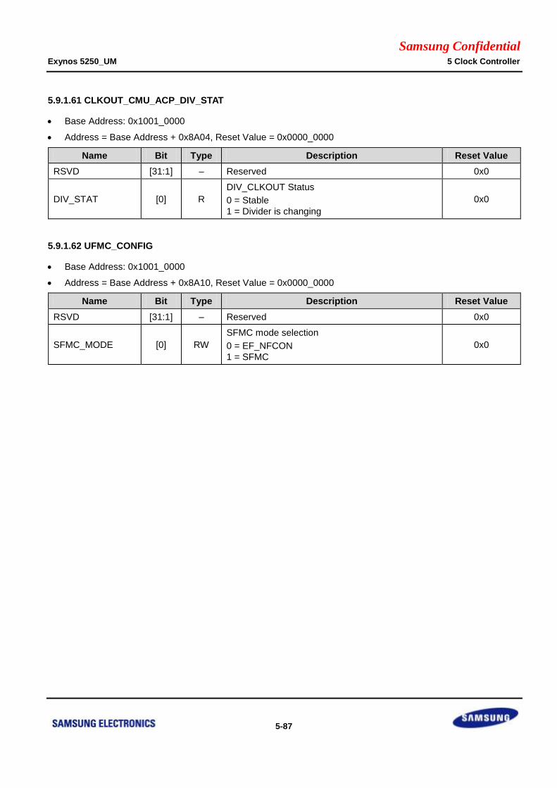
Samsung Confidential Exynos 5250_UM 5 Clock Controller
5-87
5.9.1.61 CLKOUT_CMU_ACP_DIV_STAT
Base Address: 0x1001_0000
Address = Base Address + 0x8A04, Reset Value = 0x0000_0000
Name Bit Type Description Reset Value
RSVD [31:1] – Reserved 0x0
DIV_STAT [0] R
DIV_CLKOUT Status
0 = Stable
1 = Divider is changing
0x0
5.9.1.62 UFMC_CONFIG
Base Address: 0x1001_0000
Address = Base Address + 0x8A10, Reset Value = 0x0000_0000
Name Bit Type Description Reset Value
RSVD [31:1] – Reserved 0x0
SFMC_MODE [0] RW
SFMC mode selection
0 = EF_NFCON
1 = SFMC
0x0
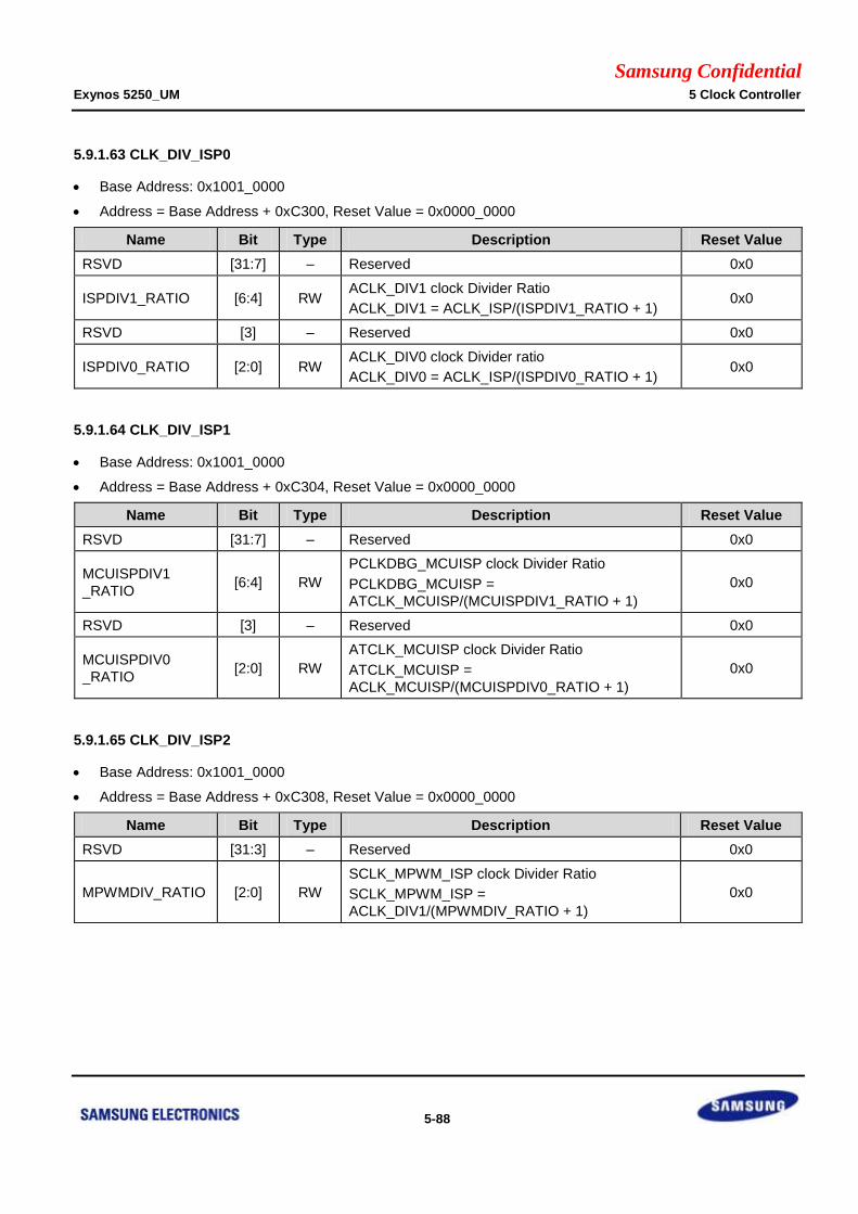
Samsung Confidential Exynos 5250_UM 5 Clock Controller
5-88
5.9.1.63 CLK_DIV_ISP0
Base Address: 0x1001_0000
Address = Base Address + 0xC300, Reset Value = 0x0000_0000
Name Bit Type Description Reset Value
RSVD [31:7] – Reserved 0x0
ISPDIV1_RATIO [6:4] RW ACLK_DIV1 clock Divider Ratio
ACLK_DIV1 = ACLK_ISP/(ISPDIV1_RATIO + 1) 0x0
RSVD [3] – Reserved 0x0
ISPDIV0_RATIO [2:0] RW ACLK_DIV0 clock Divider ratio
ACLK_DIV0 = ACLK_ISP/(ISPDIV0_RATIO + 1) 0x0
5.9.1.64 CLK_DIV_ISP1
Base Address: 0x1001_0000
Address = Base Address + 0xC304, Reset Value = 0x0000_0000
Name Bit Type Description Reset Value
RSVD [31:7] – Reserved 0x0
MCUISPDIV1
_RATIO [6:4] RW
PCLKDBG_MCUISP clock Divider Ratio
PCLKDBG_MCUISP =
ATCLK_MCUISP/(MCUISPDIV1_RATIO + 1)
0x0
RSVD [3] – Reserved 0x0
MCUISPDIV0
_RATIO [2:0] RW
ATCLK_MCUISP clock Divider Ratio
ATCLK_MCUISP =
ACLK_MCUISP/(MCUISPDIV0_RATIO + 1)
0x0
5.9.1.65 CLK_DIV_ISP2
Base Address: 0x1001_0000
Address = Base Address + 0xC308, Reset Value = 0x0000_0000
Name Bit Type Description Reset Value
RSVD [31:3] – Reserved 0x0
MPWMDIV_RATIO [2:0] RW
SCLK_MPWM_ISP clock Divider Ratio
SCLK_MPWM_ISP =
ACLK_DIV1/(MPWMDIV_RATIO + 1)
0x0

Samsung Confidential Exynos 5250_UM 5 Clock Controller
5-89
5.9.1.66 CLK_DIV_STAT_ISP0
Base Address: 0x1001_0000
Address = Base Address + 0xC400, Reset Value = 0x0000_0000
Name Bit Type Description Reset Value
RSVD [31:5] – Reserved 0x0
DIV_ISPDIV1 [4] R
DIV_ISPDIV1 status
0 = Stable
1 = Divider is changing
0x0
RSVD [3:1] – Reserved 0x0
DIV_ISPDIV0 [0] R
DIV_ISPDIV0 status
0 = Stable
1 = Divider is changing
0x0
5.9.1.67 CLK_DIV_STAT_ISP1
Base Address: 0x1001_0000
Address = Base Address + 0xC404, Reset Value = 0x0000_0000
Name Bit Type Description Reset Value
RSVD [31:5] – Reserved 0x0
DIV_MCUISPDIV1 [4] R
DIV_MCUISPDIV1 status
0 = Stable
1 = Divider is changing
0x0
RSVD [3:1] – Reserved 0x0
DIV_MCUISPDIV0 [0] R
DIV_MCUISPDIV0 status
0 = Stable
1 = Divider is changing
0x0
5.9.1.68 CLK_DIV_STAT_ISP2
Base Address: 0x1001_0000
Address = Base Address + 0xC408, Reset Value = 0x0000_0000
Name Bit Type Description Reset Value
RSVD [31:1] – Reserved 0x0
DIV_MPWMIDV [0] R
DIV_MPWMDIV status
0 = Stable
1 = Divider is changing
0x0

Samsung Confidential Exynos 5250_UM 5 Clock Controller
5-90
5.9.1.69 CLK_GATE_IP_ISP0
Base Address: 0x1001_0000
Address = Base Address + 0xC800, Reset Value = 0xFFFF_FFFF
Name Bit Type Description Reset Value
CLK_UART_ISP [31] RW
Gating all Clocks for UART_ISP
0 = Masks
1 = Passes
0x1
CLK_WDT_ISP [30] RW
Gating all Clocks for WDT_ISP
0 = Masks
1 = Passes
0x1
RSVD [29] – Reserved 0x1
CLK_PWM_ISP [28] RW
Gating all Clocks for PWM_ISP
0 = Masks
1 = Passes
0x1
CLK_MTCADC
_ISP [27] RW
Gating all Clocks for MTCADC_ISP
0 = Masks
1 = Passes
0x1
CLK_I2C1_ISP [26] RW
Gating all Clocks for I2C1_ISP
0 = Masks
1 = Passes
0x1
CLK_I2C0_ISP [25] RW
Gating all Clocks for I2C0_ISP
0 = Masks
1 = Passes
0x1
CLK_MPWM_ISP [24] RW
Gating all Clocks for MPWM_ISP
0 = Masks
1 = Passes
0x1
CLK_MCUCTL
_ISP [23] RW
Gating all Clocks for MCUCTL_ISP
0 = Masks
1 = Passes
0x1
CLK_INT_COMB
_ISP [22] RW
Gating all Clocks for INT_COMB_ISP
0 = Masks
1 = Passes
0x1
RSVD [21:14] – Reserved 0xFF
CLK_SMMU
_MCUISP [13] RW
Gating all Clocks for SMMU_MCUISP
0 = Masks
1 = Passes
0x1
CLK_SMMU
_SCALERP [12] RW
Gating all Clocks for SMMU_SCALERP
0 = Masks
1 = Passes
0x1
CLK_SMMU
_SCALERC [11] RW
Gating all Clocks for SMMU_SCALERC
0 = Masks
1 = Passes
0x1
CLK_SMMU_FD [10] RW Gating all Clocks for SMMU_FD 0x1
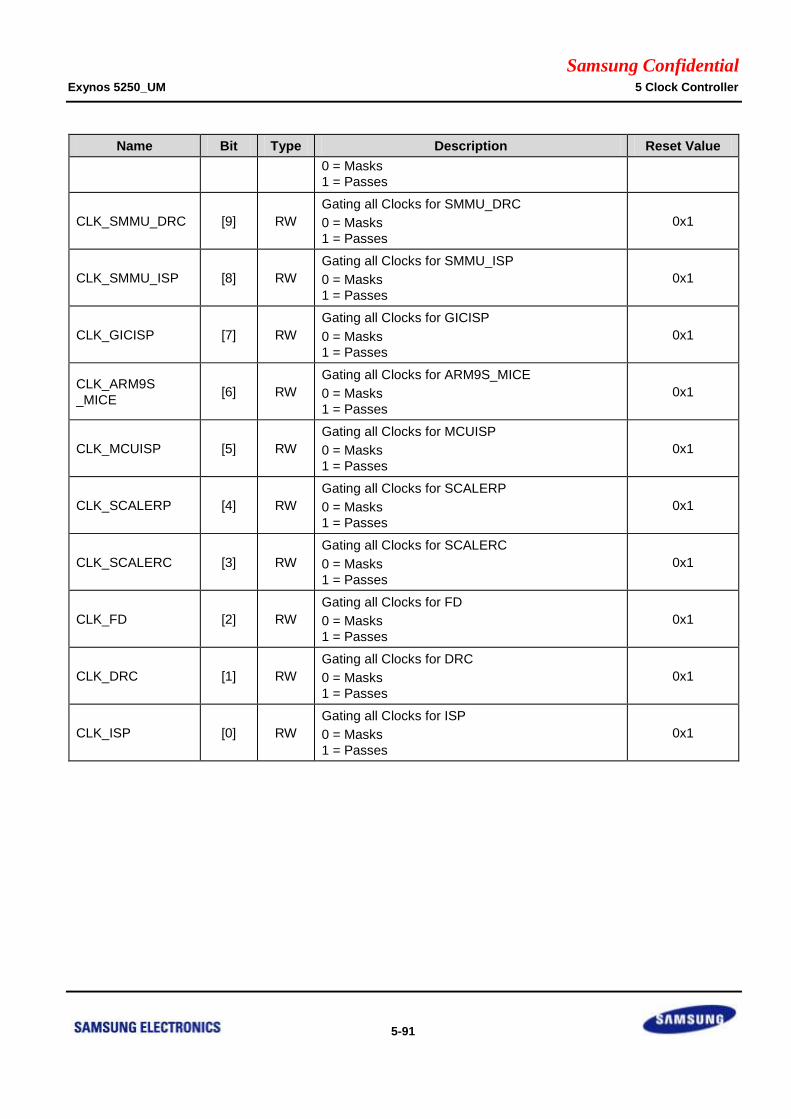
Samsung Confidential Exynos 5250_UM 5 Clock Controller
5-91
Name Bit Type Description Reset Value
0 = Masks
1 = Passes
CLK_SMMU_DRC [9] RW
Gating all Clocks for SMMU_DRC
0 = Masks
1 = Passes
0x1
CLK_SMMU_ISP [8] RW
Gating all Clocks for SMMU_ISP
0 = Masks
1 = Passes
0x1
CLK_GICISP [7] RW
Gating all Clocks for GICISP
0 = Masks
1 = Passes
0x1
CLK_ARM9S
_MICE [6] RW
Gating all Clocks for ARM9S_MICE
0 = Masks
1 = Passes
0x1
CLK_MCUISP [5] RW
Gating all Clocks for MCUISP
0 = Masks
1 = Passes
0x1
CLK_SCALERP [4] RW
Gating all Clocks for SCALERP
0 = Masks
1 = Passes
0x1
CLK_SCALERC [3] RW
Gating all Clocks for SCALERC
0 = Masks
1 = Passes
0x1
CLK_FD [2] RW
Gating all Clocks for FD
0 = Masks
1 = Passes
0x1
CLK_DRC [1] RW
Gating all Clocks for DRC
0 = Masks
1 = Passes
0x1
CLK_ISP [0] RW
Gating all Clocks for ISP
0 = Masks
1 = Passes
0x1

Samsung Confidential Exynos 5250_UM 5 Clock Controller
5-92
5.9.1.70 CLK_GATE_IP_ISP1
Base Address: 0x1001_0000
Address = Base Address + 0xC804, Reset Value = 0xFFFF_FFFF
Name Bit Type Description Reset Value
RSVD [31:14] RW Reserved 0x3_FFFF
CLK_SPI1_ISP [13] RW
Gating all Clocks for SPI1_ISP
0 = Masks
1 = Passes
0x1
CLK_SPI0_ISP [12] RW
Gating all Clocks for SPI0_ISP
0 = Masks
1 = Passes
0x1
RSVD [11:8] – Reserved 0xF
CLK_SMMU3DNR [7] RW
Gating all Clocks for SMMU3DNR
0 = Masks
1 = Passes
0x1
CLK_SMMUDIS1 [6] RW
Gating all Clocks for SMMUDIS1
0 = Masks
1 = Passes
0x1
CLK_SMMUDIS0 [5] RW
Gating all Clocks for SMMUDIS0
0 = Masks
1 = Passes
0x1
CLK_SMMUODC [4] RW
Gating all Clocks for SMMUODC
0 = Masks
1 = Passes
0x1
RSVD [3] RW Reserved 0x1
CLK_3DNR [2] RW
Gating all Clocks for 3DNR
0 = Masks
1 = Passes
0x1
CLK_DIS [1] RW
Gating all Clocks for DIS
0 = Masks
1 = Passes
0x1
CLK_ODC [0] RW
Gating all Clocks for ODC
0 = Masks
1 = Passes
0x1
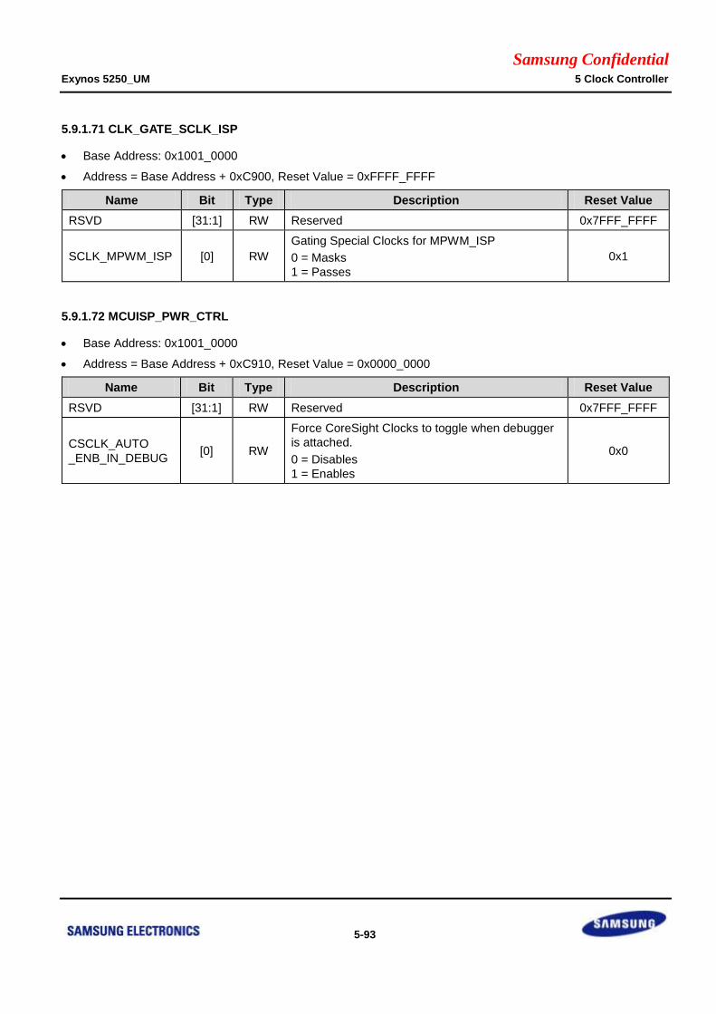
Samsung Confidential Exynos 5250_UM 5 Clock Controller
5-93
5.9.1.71 CLK_GATE_SCLK_ISP
Base Address: 0x1001_0000
Address = Base Address + 0xC900, Reset Value = 0xFFFF_FFFF
Name Bit Type Description Reset Value
RSVD [31:1] RW Reserved 0x7FFF_FFFF
SCLK_MPWM_ISP [0] RW
Gating Special Clocks for MPWM_ISP
0 = Masks
1 = Passes
0x1
5.9.1.72 MCUISP_PWR_CTRL
Base Address: 0x1001_0000
Address = Base Address + 0xC910, Reset Value = 0x0000_0000
Name Bit Type Description Reset Value
RSVD [31:1] RW Reserved 0x7FFF_FFFF
CSCLK_AUTO
_ENB_IN_DEBUG [0] RW
Force CoreSight Clocks to toggle when debugger
is attached.
0 = Disables
1 = Enables
0x0
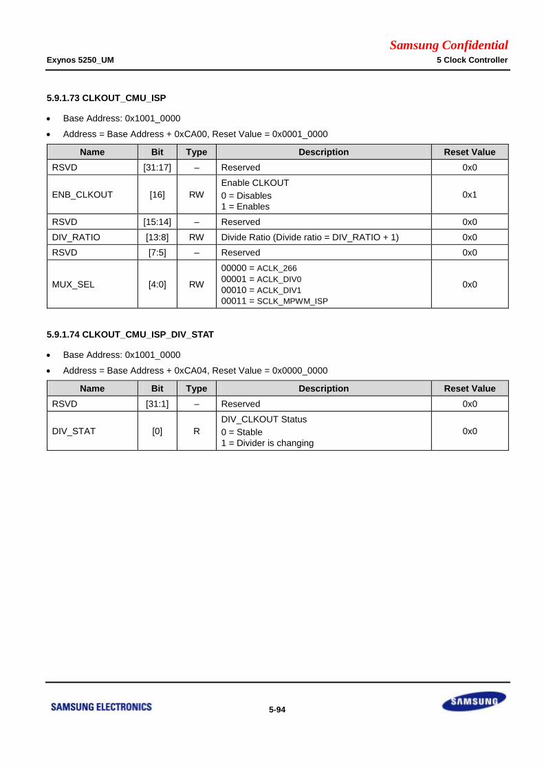
Samsung Confidential Exynos 5250_UM 5 Clock Controller
5-94
5.9.1.73 CLKOUT_CMU_ISP
Base Address: 0x1001_0000
Address = Base Address + 0xCA00, Reset Value = 0x0001_0000
Name Bit Type Description Reset Value
RSVD [31:17] – Reserved 0x0
ENB_CLKOUT [16] RW
Enable CLKOUT
0 = Disables
1 = Enables
0x1
RSVD [15:14] – Reserved 0x0
DIV_RATIO [13:8] RW Divide Ratio (Divide ratio = DIV_RATIO + 1) 0x0
RSVD [7:5] – Reserved 0x0
MUX_SEL [4:0] RW
00000 = ACLK_266
00001 = ACLK_DIV0
00010 = ACLK_DIV1
00011 = SCLK_MPWM_ISP
0x0
5.9.1.74 CLKOUT_CMU_ISP_DIV_STAT
Base Address: 0x1001_0000
Address = Base Address + 0xCA04, Reset Value = 0x0000_0000
Name Bit Type Description Reset Value
RSVD [31:1] – Reserved 0x0
DIV_STAT [0] R
DIV_CLKOUT Status
0 = Stable
1 = Divider is changing
0x0
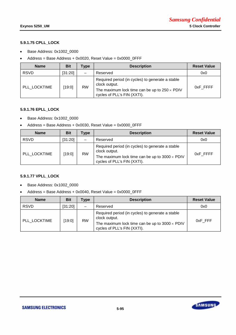
Samsung Confidential Exynos 5250_UM 5 Clock Controller
5-95
5.9.1.75 CPLL_LOCK
Base Address: 0x1002_0000
Address = Base Address + 0x0020, Reset Value = 0x0000_0FFF
Name Bit Type Description Reset Value
RSVD [31:20] – Reserved 0x0
PLL_LOCKTIME [19:0] RW
Required period (in cycles) to generate a stable
clock output.
The maximum lock time can be up to 250 PDIV
cycles of PLL's FIN (XXTI).
0xF_FFFF
5.9.1.76 EPLL_LOCK
Base Address: 0x1002_0000
Address = Base Address + 0x0030, Reset Value = 0x0000_0FFF
Name Bit Type Description Reset Value
RSVD [31:20] – Reserved 0x0
PLL_LOCKTIME [19:0] RW
Required period (in cycles) to generate a stable
clock output.
The maximum lock time can be up to 3000 PDIV
cycles of PLL's FIN (XXTI).
0xF_FFFF
5.9.1.77 VPLL_LOCK
Base Address: 0x1002_0000
Address = Base Address + 0x0040, Reset Value = 0x0000_0FFF
Name Bit Type Description Reset Value
RSVD [31:20] – Reserved 0x0
PLL_LOCKTIME [19:0] RW
Required period (in cycles) to generate a stable
clock output.
The maximum lock time can be up to 3000 PDIV
cycles of PLL's FIN (XXTI).
0xF_FFF
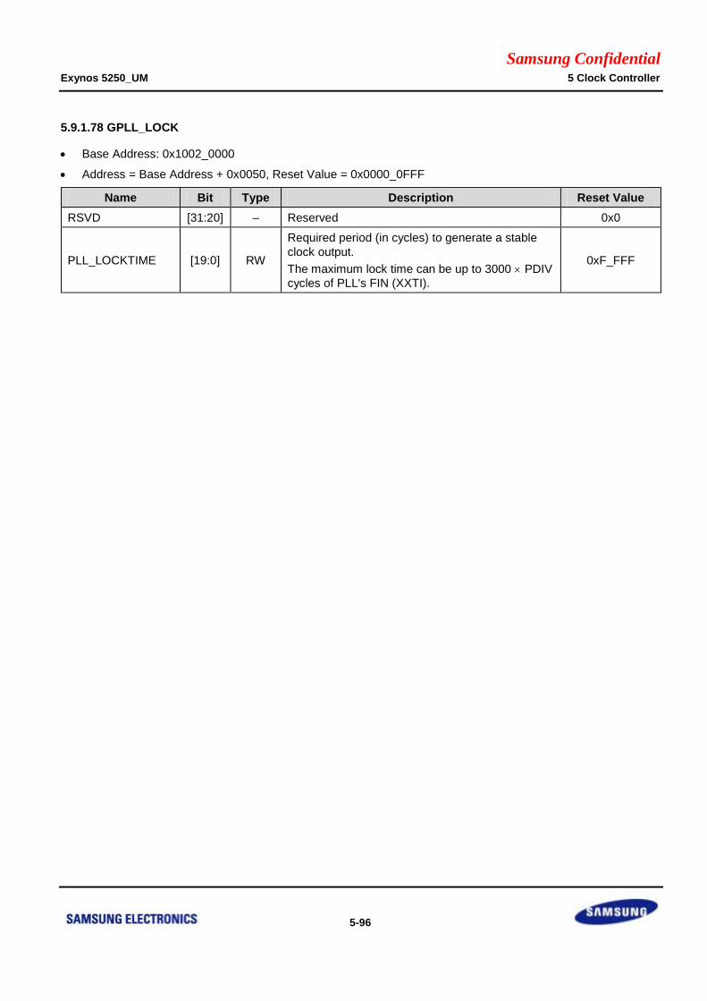
Samsung Confidential Exynos 5250_UM 5 Clock Controller
5-96
5.9.1.78 GPLL_LOCK
Base Address: 0x1002_0000
Address = Base Address + 0x0050, Reset Value = 0x0000_0FFF
Name Bit Type Description Reset Value
RSVD [31:20] – Reserved 0x0
PLL_LOCKTIME [19:0] RW
Required period (in cycles) to generate a stable
clock output.
The maximum lock time can be up to 3000 PDIV
cycles of PLL's FIN (XXTI).
0xF_FFF
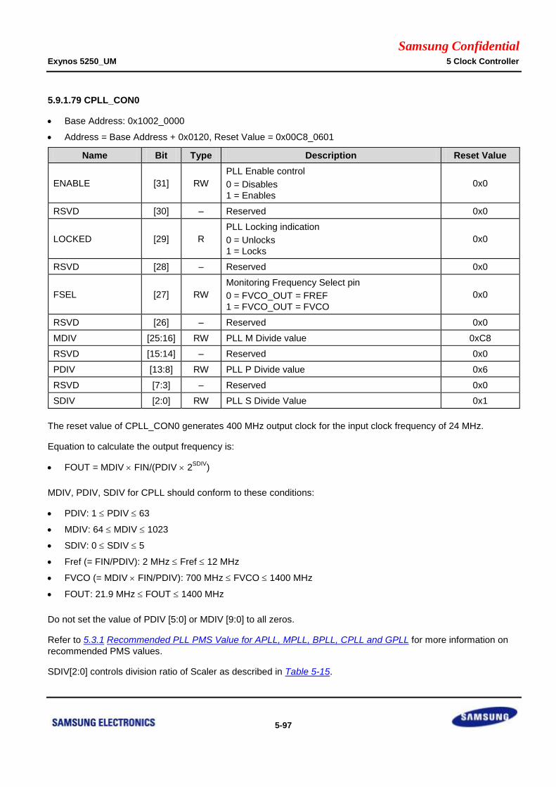
Samsung Confidential Exynos 5250_UM 5 Clock Controller
5-97
5.9.1.79 CPLL_CON0
Base Address: 0x1002_0000
Address = Base Address + 0x0120, Reset Value = 0x00C8_0601
Name Bit Type Description Reset Value
ENABLE [31] RW
PLL Enable control
0 = Disables
1 = Enables
0x0
RSVD [30] – Reserved 0x0
LOCKED [29] R
PLL Locking indication
0 = Unlocks
1 = Locks
0x0
RSVD [28] – Reserved 0x0
FSEL [27] RW
Monitoring Frequency Select pin
0 = FVCO_OUT = FREF
1 = FVCO_OUT = FVCO
0x0
RSVD [26] – Reserved 0x0
MDIV [25:16] RW PLL M Divide value 0xC8
RSVD [15:14] – Reserved 0x0
PDIV [13:8] RW PLL P Divide value 0x6
RSVD [7:3] – Reserved 0x0
SDIV [2:0] RW PLL S Divide Value 0x1
The reset value of CPLL_CON0 generates 400 MHz output clock for the input clock frequency of 24 MHz.
Equation to calculate the output frequency is:
FOUT = MDIV FIN/(PDIV 2SDIV
)
MDIV, PDIV, SDIV for CPLL should conform to these conditions:
PDIV: 1 PDIV 63
MDIV: 64 MDIV 1023
SDIV: 0 SDIV 5
Fref (= FIN/PDIV): 2 MHz Fref 12 MHz
FVCO (= MDIV FIN/PDIV): 700 MHz FVCO 1400 MHz
FOUT: 21.9 MHz FOUT 1400 MHz
Do not set the value of PDIV [5:0] or MDIV [9:0] to all zeros.
Refer to 5.3.1 Recommended PLL PMS Value for APLL, MPLL, BPLL, CPLL and GPLL for more information on
recommended PMS values.
SDIV[2:0] controls division ratio of Scaler as described in Table 5-15.
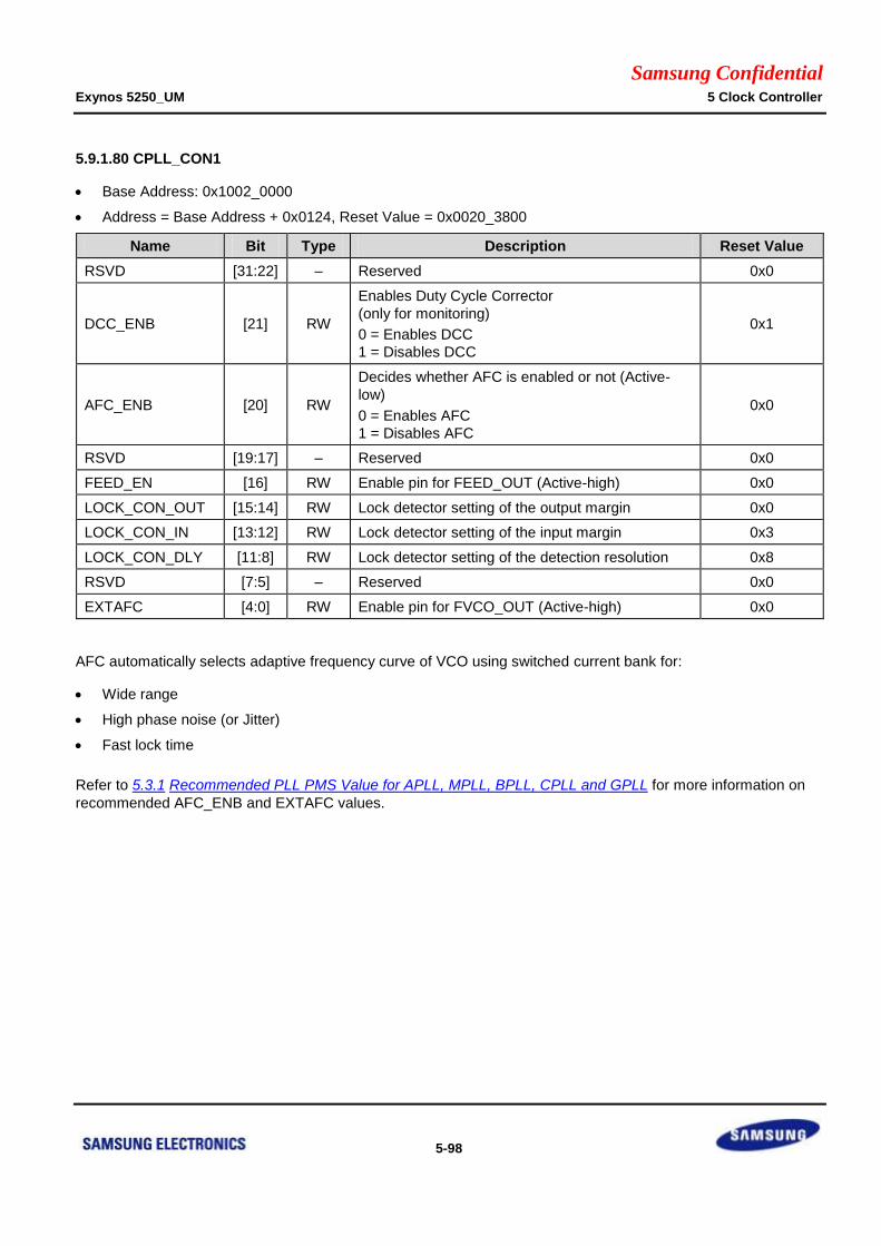
Samsung Confidential Exynos 5250_UM 5 Clock Controller
5-98
5.9.1.80 CPLL_CON1
Base Address: 0x1002_0000
Address = Base Address + 0x0124, Reset Value = 0x0020_3800
Name Bit Type Description Reset Value
RSVD [31:22] – Reserved 0x0
DCC_ENB [21] RW
Enables Duty Cycle Corrector
(only for monitoring)
0 = Enables DCC
1 = Disables DCC
0x1
AFC_ENB [20] RW
Decides whether AFC is enabled or not (Active-
low)
0 = Enables AFC
1 = Disables AFC
0x0
RSVD [19:17] – Reserved 0x0
FEED_EN [16] RW Enable pin for FEED_OUT (Active-high) 0x0
LOCK_CON_OUT [15:14] RW Lock detector setting of the output margin 0x0
LOCK_CON_IN [13:12] RW Lock detector setting of the input margin 0x3
LOCK_CON_DLY [11:8] RW Lock detector setting of the detection resolution 0x8
RSVD [7:5] – Reserved 0x0
EXTAFC [4:0] RW Enable pin for FVCO_OUT (Active-high) 0x0
AFC automatically selects adaptive frequency curve of VCO using switched current bank for:
Wide range
High phase noise (or Jitter)
Fast lock time
Refer to 5.3.1 Recommended PLL PMS Value for APLL, MPLL, BPLL, CPLL and GPLL for more information on
recommended AFC_ENB and EXTAFC values.

Samsung Confidential Exynos 5250_UM 5 Clock Controller
5-99
5.9.1.81 EPLL_CON0
Base Address: 0x1002_0000
Address = Base Address + 0x0130, Reset Value = 0x0030_0301
Name Bit Type Description Reset Value
ENABLE [31] RW
PLL Enable control
0 = Disables
1 = Enables
0x0
RSVD [30] – Reserved 0x0
LOCKED [29] R
PLL locking indication
0 = Unlocks
1 = Locks
0x0
RSVD [28:25] – Reserved 0x0
MDIV [24:16] RW PLL M Divide Value 0x30
RSVD [15:14] – Reserved 0x0
PDIV [13:8] RW PLL P Divide Value 0x3
RSVD [7:3] – Reserved 0x0
SDIV [2:0] RW PLL S Divide Value 0x1
The reset value of EPLL_CON0 generates 192 MHz output clock for the input clock frequency of 24 MHz.
Equation to calculate the output frequency is:
FOUT = (MDIV + K/65536) FIN/(PDIV 2SDIV
)
MDIV, PDIV, SDIV for EPLL should conform to these conditions:
PDIV: 1 PDIV 63
MDIV: 64 MDIV 511
SDIV: 0 SDIV 5
K: – 32768 K 32767 (K[15:0] is a two's complement integer)
Fref (= FIN/PDIV): 2 MHz Fref 30 MHz
FVCO (= (MDIV + K/65536) FIN/PDIV): 700 MHz FVCO 1400 MHz
FOUT: 22 MHz FOUT 1400 MHz
Do not set the value PDIV or MDIV to all zeros.
SDIV[2:0] controls division ratio of Scaler as described in Table 5-15.
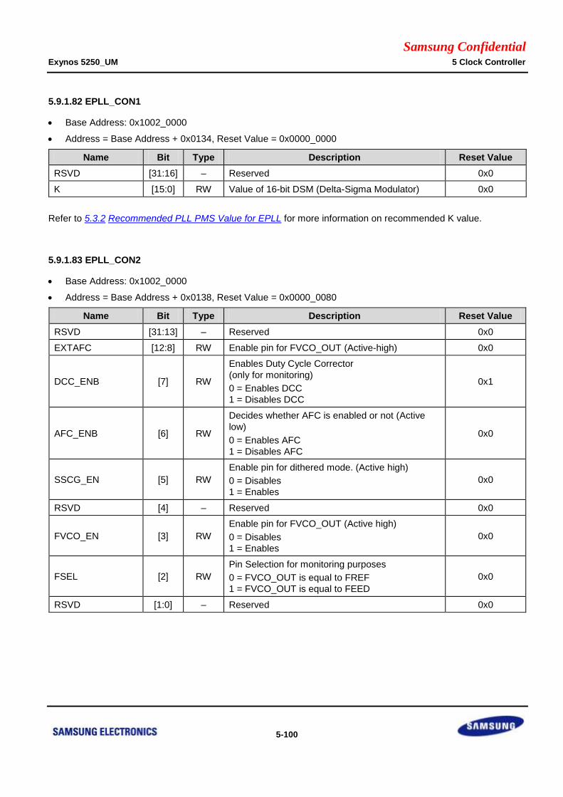
Samsung Confidential Exynos 5250_UM 5 Clock Controller
5-100
5.9.1.82 EPLL_CON1
Base Address: 0x1002_0000
Address = Base Address + 0x0134, Reset Value = 0x0000_0000
Name Bit Type Description Reset Value
RSVD [31:16] – Reserved 0x0
K [15:0] RW Value of 16-bit DSM (Delta-Sigma Modulator) 0x0
Refer to 5.3.2 Recommended PLL PMS Value for EPLL for more information on recommended K value.
5.9.1.83 EPLL_CON2
Base Address: 0x1002_0000
Address = Base Address + 0x0138, Reset Value = 0x0000_0080
Name Bit Type Description Reset Value
RSVD [31:13] – Reserved 0x0
EXTAFC [12:8] RW Enable pin for FVCO_OUT (Active-high) 0x0
DCC_ENB [7] RW
Enables Duty Cycle Corrector
(only for monitoring)
0 = Enables DCC
1 = Disables DCC
0x1
AFC_ENB [6] RW
Decides whether AFC is enabled or not (Active
low)
0 = Enables AFC
1 = Disables AFC
0x0
SSCG_EN [5] RW
Enable pin for dithered mode. (Active high)
0 = Disables
1 = Enables
0x0
RSVD [4] – Reserved 0x0
FVCO_EN [3] RW
Enable pin for FVCO_OUT (Active high)
0 = Disables
1 = Enables
0x0
FSEL [2] RW
Pin Selection for monitoring purposes
0 = FVCO_OUT is equal to FREF
1 = FVCO_OUT is equal to FEED
0x0
RSVD [1:0] – Reserved 0x0
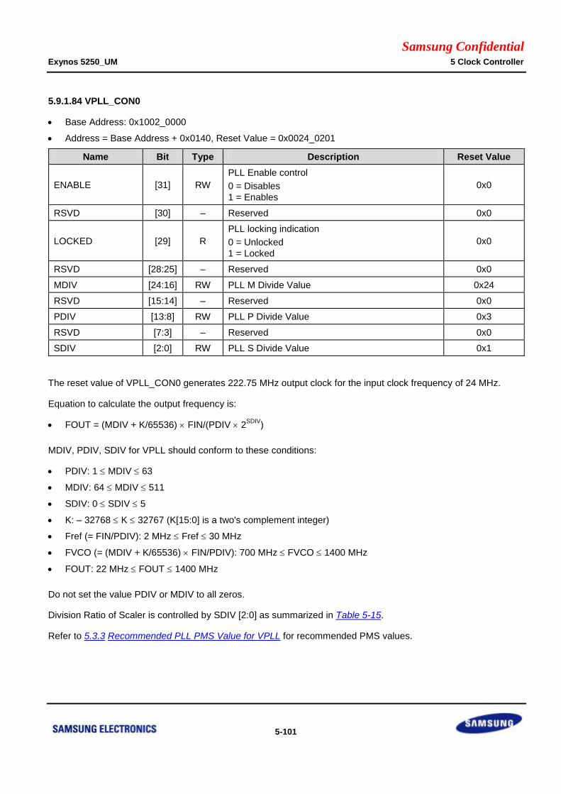
Samsung Confidential Exynos 5250_UM 5 Clock Controller
5-101
5.9.1.84 VPLL_CON0
Base Address: 0x1002_0000
Address = Base Address + 0x0140, Reset Value = 0x0024_0201
Name Bit Type Description Reset Value
ENABLE [31] RW
PLL Enable control
0 = Disables
1 = Enables
0x0
RSVD [30] – Reserved 0x0
LOCKED [29] R
PLL locking indication
0 = Unlocked
1 = Locked
0x0
RSVD [28:25] – Reserved 0x0
MDIV [24:16] RW PLL M Divide Value 0x24
RSVD [15:14] – Reserved 0x0
PDIV [13:8] RW PLL P Divide Value 0x3
RSVD [7:3] – Reserved 0x0
SDIV [2:0] RW PLL S Divide Value 0x1
The reset value of VPLL_CON0 generates 222.75 MHz output clock for the input clock frequency of 24 MHz.
Equation to calculate the output frequency is:
FOUT = (MDIV + K/65536) FIN/(PDIV 2SDIV
)
MDIV, PDIV, SDIV for VPLL should conform to these conditions:
PDIV: 1 MDIV 63
MDIV: 64 MDIV 511
SDIV: 0 SDIV 5
K: – 32768 K 32767 (K[15:0] is a two's complement integer)
Fref (= FIN/PDIV): 2 MHz Fref 30 MHz
FVCO (= (MDIV + K/65536) FIN/PDIV): 700 MHz FVCO 1400 MHz
FOUT: 22 MHz FOUT 1400 MHz
Do not set the value PDIV or MDIV to all zeros.
Division Ratio of Scaler is controlled by SDIV [2:0] as summarized in Table 5-15.
Refer to 5.3.3 Recommended PLL PMS Value for VPLL for recommended PMS values.
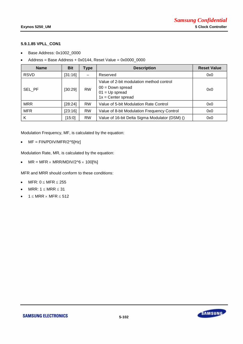
Samsung Confidential Exynos 5250_UM 5 Clock Controller
5-102
5.9.1.85 VPLL_CON1
Base Address: 0x1002_0000
Address = Base Address + 0x0144, Reset Value = 0x0000_0000
Name Bit Type Description Reset Value
RSVD [31:16] – Reserved 0x0
SEL_PF [30:29] RW
Value of 2-bit modulation method control
00 = Down spread
01 = Up spread
1x = Center spread
0x0
MRR [28:24] RW Value of 5-bit Modulation Rate Control 0x0
MFR [23:16] RW Value of 8-bit Modulation Frequency Control 0x0
K [15:0] RW Value of 16-bit Delta Sigma Modulator (DSM) () 0x0
Modulation Frequency, MF, is calculated by the equation:
MF = FIN/PDIV/MFR/2^5[Hz]
Modulation Rate, MR, is calculated by the equation:
MR = MFR MRR/MDIV/2^6 100[%]
MFR and MRR should conform to these conditions:
MFR: 0 MFR 255
MRR: 1 MRR 31
1 MRR MFR 512
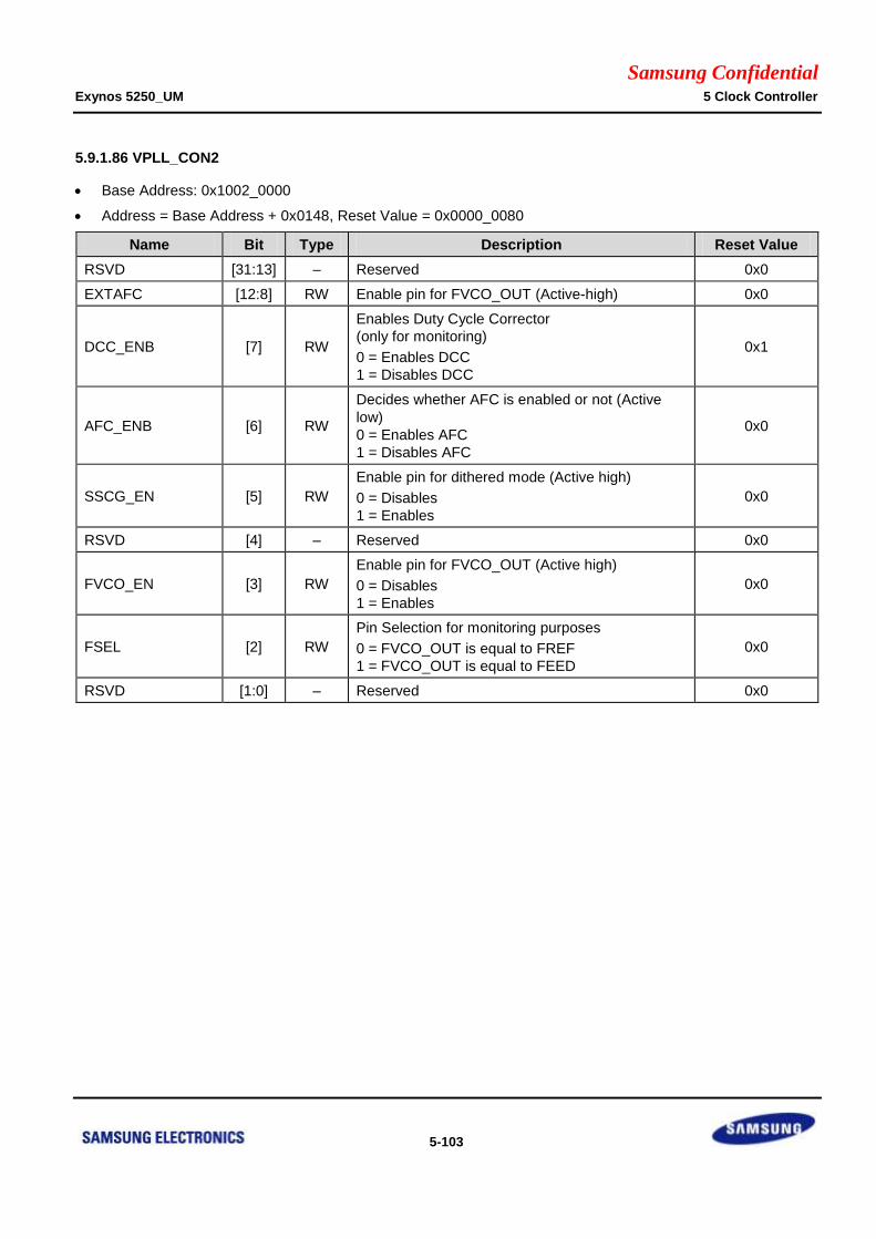
Samsung Confidential Exynos 5250_UM 5 Clock Controller
5-103
5.9.1.86 VPLL_CON2
Base Address: 0x1002_0000
Address = Base Address + 0x0148, Reset Value = 0x0000_0080
Name Bit Type Description Reset Value
RSVD [31:13] – Reserved 0x0
EXTAFC [12:8] RW Enable pin for FVCO_OUT (Active-high) 0x0
DCC_ENB [7] RW
Enables Duty Cycle Corrector
(only for monitoring)
0 = Enables DCC
1 = Disables DCC
0x1
AFC_ENB [6] RW
Decides whether AFC is enabled or not (Active
low)
0 = Enables AFC
1 = Disables AFC
0x0
SSCG_EN [5] RW
Enable pin for dithered mode (Active high)
0 = Disables
1 = Enables
0x0
RSVD [4] – Reserved 0x0
FVCO_EN [3] RW
Enable pin for FVCO_OUT (Active high)
0 = Disables
1 = Enables
0x0
FSEL [2] RW
Pin Selection for monitoring purposes
0 = FVCO_OUT is equal to FREF
1 = FVCO_OUT is equal to FEED
0x0
RSVD [1:0] – Reserved 0x0
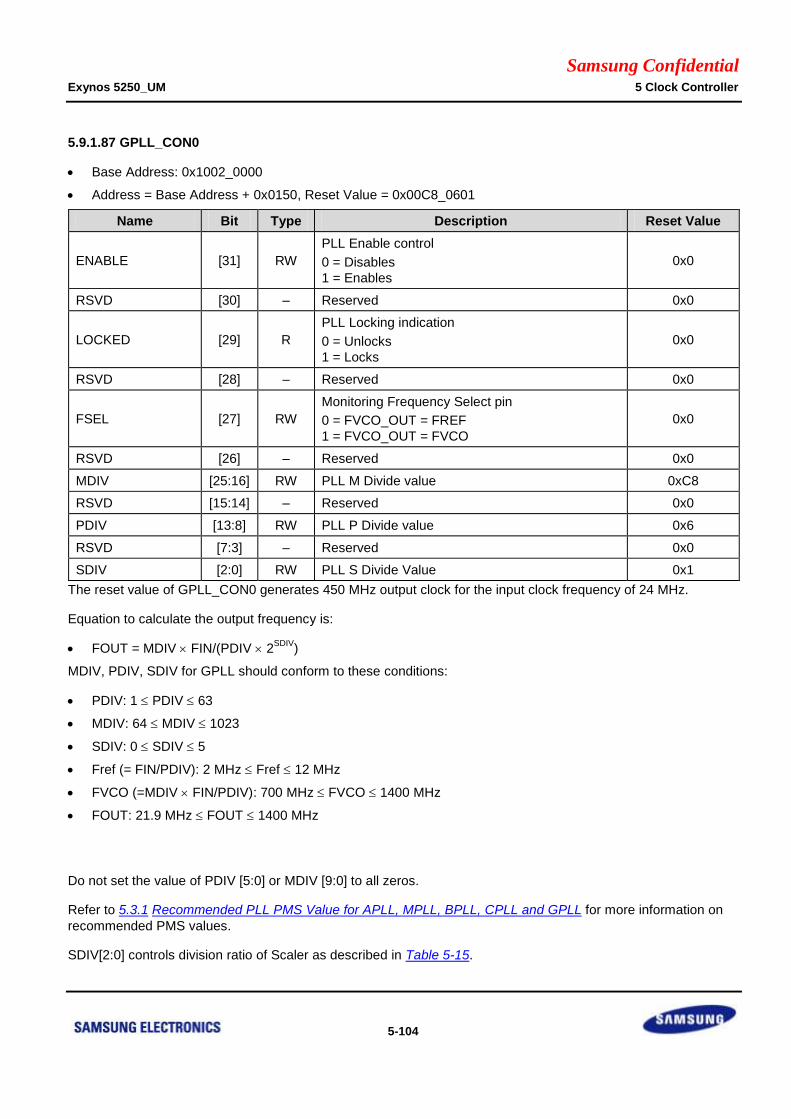
Samsung Confidential Exynos 5250_UM 5 Clock Controller
5-104
5.9.1.87 GPLL_CON0
Base Address: 0x1002_0000
Address = Base Address + 0x0150, Reset Value = 0x00C8_0601
Name Bit Type Description Reset Value
ENABLE [31] RW
PLL Enable control
0 = Disables
1 = Enables
0x0
RSVD [30] – Reserved 0x0
LOCKED [29] R
PLL Locking indication
0 = Unlocks
1 = Locks
0x0
RSVD [28] – Reserved 0x0
FSEL [27] RW
Monitoring Frequency Select pin
0 = FVCO_OUT = FREF
1 = FVCO_OUT = FVCO
0x0
RSVD [26] – Reserved 0x0
MDIV [25:16] RW PLL M Divide value 0xC8
RSVD [15:14] – Reserved 0x0
PDIV [13:8] RW PLL P Divide value 0x6
RSVD [7:3] – Reserved 0x0
SDIV [2:0] RW PLL S Divide Value 0x1
The reset value of GPLL_CON0 generates 450 MHz output clock for the input clock frequency of 24 MHz.
Equation to calculate the output frequency is:
FOUT = MDIV FIN/(PDIV 2SDIV
)
MDIV, PDIV, SDIV for GPLL should conform to these conditions:
PDIV: 1 PDIV 63
MDIV: 64 MDIV 1023
SDIV: 0 SDIV 5
Fref (= FIN/PDIV): 2 MHz Fref 12 MHz
FVCO (=MDIV FIN/PDIV): 700 MHz FVCO 1400 MHz
FOUT: 21.9 MHz FOUT 1400 MHz
Do not set the value of PDIV [5:0] or MDIV [9:0] to all zeros.
Refer to 5.3.1 Recommended PLL PMS Value for APLL, MPLL, BPLL, CPLL and GPLL for more information on
recommended PMS values.
SDIV[2:0] controls division ratio of Scaler as described in Table 5-15.

Samsung Confidential Exynos 5250_UM 5 Clock Controller
5-105
5.9.1.88 GPLL_CON1
Base Address: 0x1002_0000
Address = Base Address + 0x0154, Reset Value = 0x0020_3800
Name Bit Type Description Reset Value
RSVD [31:22] – Reserved 0x0
DCC_ENB [21] RW
Enables Duty Cycle Corrector
(only for monitoring)
0 = Enables DCC
1 = Disables DCC
0x1
AFC_ENB [20] RW
Decides whether AFC is enabled or not (Active-
low)
0 = Enables AFC
1 = Disables AFC
0x0
RSVD [19:17] – Reserved 0x0
FEED_EN [16] RW Enable pin for FEED_OUT (Active-high) 0x0
LOCK_CON_OUT [15:14] RW Lock detector setting of the output margin 0x0
LOCK_CON_IN [13:12] RW Lock detector setting of the input margin 0x3
LOCK_CON_DLY [11:8] RW Lock detector setting of the detection resolution 0x8
RSVD [7:5] – Reserved 0x0
EXTAFC [4:0] RW Enable pin for FVCO_OUT (Active-high) 0x0
AFC automatically selects adaptive frequency curve of VCO using switched current bank for:
Wide range
High phase noise (or Jitter)
Fast lock time
Refer to 5.3.1 Recommended PLL PMS Value for APLL, MPLL, BPLL, CPLL and GPLL for more information on
recommended AFC_ENB and EXTAFC values.
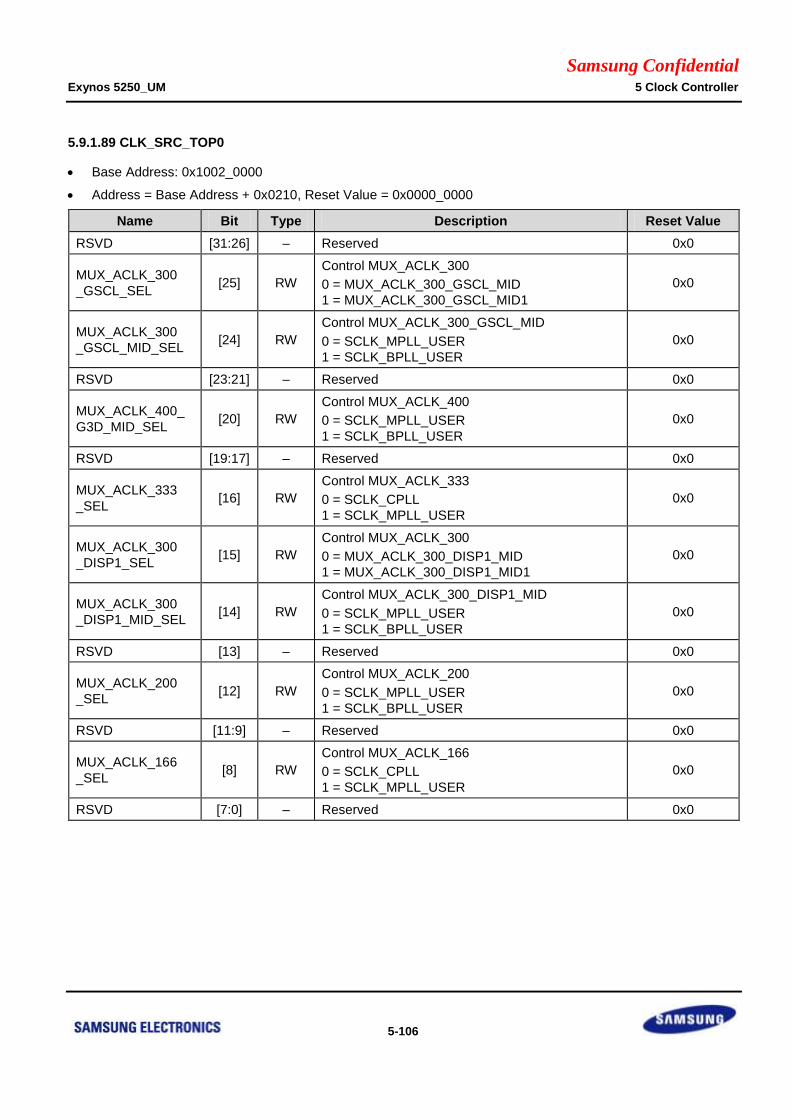
Samsung Confidential Exynos 5250_UM 5 Clock Controller
5-106
5.9.1.89 CLK_SRC_TOP0
Base Address: 0x1002_0000
Address = Base Address + 0x0210, Reset Value = 0x0000_0000
Name Bit Type Description Reset Value
RSVD [31:26] – Reserved 0x0
MUX_ACLK_300
_GSCL_SEL [25] RW
Control MUX_ACLK_300
0 = MUX_ACLK_300_GSCL_MID
1 = MUX_ACLK_300_GSCL_MID1
0x0
MUX_ACLK_300
_GSCL_MID_SEL [24] RW
Control MUX_ACLK_300_GSCL_MID
0 = SCLK_MPLL_USER
1 = SCLK_BPLL_USER
0x0
RSVD [23:21] – Reserved 0x0
MUX_ACLK_400_
G3D_MID_SEL [20] RW
Control MUX_ACLK_400
0 = SCLK_MPLL_USER
1 = SCLK_BPLL_USER
0x0
RSVD [19:17] – Reserved 0x0
MUX_ACLK_333
_SEL [16] RW
Control MUX_ACLK_333
0 = SCLK_CPLL
1 = SCLK_MPLL_USER
0x0
MUX_ACLK_300
_DISP1_SEL [15] RW
Control MUX_ACLK_300
0 = MUX_ACLK_300_DISP1_MID
1 = MUX_ACLK_300_DISP1_MID1
0x0
MUX_ACLK_300
_DISP1_MID_SEL [14] RW
Control MUX_ACLK_300_DISP1_MID
0 = SCLK_MPLL_USER
1 = SCLK_BPLL_USER
0x0
RSVD [13] – Reserved 0x0
MUX_ACLK_200
_SEL [12] RW
Control MUX_ACLK_200
0 = SCLK_MPLL_USER
1 = SCLK_BPLL_USER
0x0
RSVD [11:9] – Reserved 0x0
MUX_ACLK_166
_SEL [8] RW
Control MUX_ACLK_166
0 = SCLK_CPLL
1 = SCLK_MPLL_USER
0x0
RSVD [7:0] – Reserved 0x0
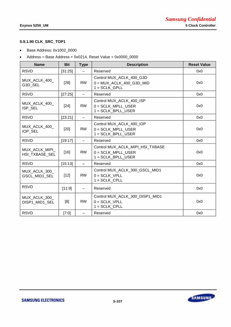
Samsung Confidential Exynos 5250_UM 5 Clock Controller
5-107
5.9.1.90 CLK_SRC_TOP1
Base Address: 0x1002_0000
Address = Base Address + 0x0214, Reset Value = 0x0000_0000
Name Bit Type Description Reset Value
RSVD [31:25] – Reserved 0x0
MUX_ACLK_400_
G3D_SEL [28] RW
Control MUX_ACLK_400_G3D
0 = MUX_ACLK_400_G3D_MID
1 = SCLK_GPLL
0x0
RSVD [27:25] – Reserved 0x0
MUX_ACLK_400_
ISP_SEL [24] RW
Control MUX_ACLK_400_ISP
0 = SCLK_MPLL_USER
1 = SCLK_BPLL_USER
0x0
RSVD [23:21] – Reserved 0x0
MUX_ACLK_400_
IOP_SEL [20] RW
Control MUX_ACLK_400_IOP
0 = SCLK_MPLL_USER
1 = SCLK_BPLL_USER
0x0
RSVD [19:17] – Reserved 0x0
MUX_ACLK_MIPI_
HSI_TXBASE_SEL [16] RW
Control MUX_ACLK_MIPI_HSI_TXBASE
0 = SCLK_MPLL_USER
1 = SCLK_BPLL_USER
0x0
RSVD [15:13] – Reserved 0x0
MUX_ACLK_300_
GSCL_MID1_SEL [12] RW
Control MUX_ACLK_300_GSCL_MID1
0 = SCLK_VPLL
1 = SCLK_CPLL
0x0
RSVD [11:9] – Reserved 0x0
MUX_ACLK_300_
DISP1_MID1_SEL [8] RW
Control MUX_ACLK_300_DISP1_MID1
0 = SCLK_VPLL
1 = SCLK_CPLL
0x0
RSVD [7:0] – Reserved 0x0

Samsung Confidential Exynos 5250_UM 5 Clock Controller
5-108
5.9.1.91 CLK_SRC_TOP2
Base Address: 0x1002_0000
Address = Base Address + 0x0218, Reset Value = 0x0000_0000
Name Bit Type Description Reset Value
RSVD [31:29] – Reserved 0x0
MUX_GPLL _SEL [28] RW
Control MUX_GPLL_USER
0 = XXTI
1 = FOUT_GPLL
0x0
RSVD [27:25] – Reserved 0x0
MUX_BPLL_USER
_SEL [24] RW
Control MUX_BPLL_USER
0 = XXTI
1 = MOUT_BPLL
0x0
RSVD [23:21] – Reserved 0x0
MUX_MPLL_USER
_SEL [20] RW
Control MUX_MPLL_USER
0 = XXTI
1 = MOUT_MPLL
0x0
RSVD [19:17] – Reserved 0x0
MUX_VPLL_SEL [16] RW
Control MUX_VPLL
0 = XXTI
1 = FOUT_VPLL
0x0
RSVD [15:13] – Reserved 0x0
MUX_EPLL_SEL [12] RW
Control MUX_EPLL
0 = XXTI
1 = FOUT_EPLL
0x0
RSVD [11:9] – Reserved 0x0
MUX_CPLL_SEL [8] RW
Control MUX_CPLL
0 = XXTI
1 = FOUT_CPLL
0x0
RSVD [7:1] – Reserved 0x0
VPLLSRC_SEL [0] RW
Control MUX_VPLLSRC
0 = XXTI
1 = SCLK_HDMI24M
0x0
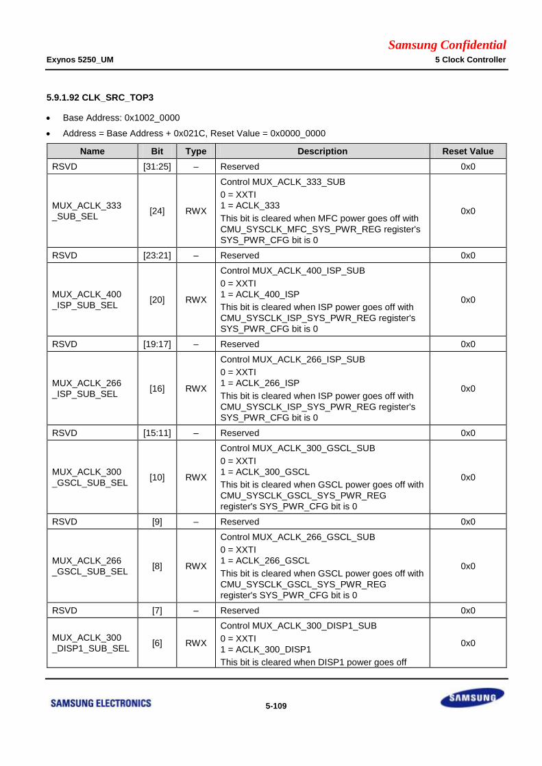
Samsung Confidential Exynos 5250_UM 5 Clock Controller
5-109
5.9.1.92 CLK_SRC_TOP3
Base Address: 0x1002_0000
Address = Base Address + 0x021C, Reset Value = 0x0000_0000
Name Bit Type Description Reset Value
RSVD [31:25] – Reserved 0x0
MUX_ACLK_333
_SUB_SEL [24] RWX
Control MUX_ACLK_333_SUB
0 = XXTI
1 = ACLK_333
This bit is cleared when MFC power goes off with
CMU_SYSCLK_MFC_SYS_PWR_REG register's
SYS_PWR_CFG bit is 0
0x0
RSVD [23:21] – Reserved 0x0
MUX_ACLK_400
_ISP_SUB_SEL [20] RWX
Control MUX_ACLK_400_ISP_SUB
0 = XXTI
1 = ACLK_400_ISP
This bit is cleared when ISP power goes off with
CMU_SYSCLK_ISP_SYS_PWR_REG register's
SYS_PWR_CFG bit is 0
0x0
RSVD [19:17] – Reserved 0x0
MUX_ACLK_266
_ISP_SUB_SEL [16] RWX
Control MUX_ACLK_266_ISP_SUB
0 = XXTI
1 = ACLK_266_ISP
This bit is cleared when ISP power goes off with
CMU_SYSCLK_ISP_SYS_PWR_REG register's
SYS_PWR_CFG bit is 0
0x0
RSVD [15:11] – Reserved 0x0
MUX_ACLK_300
_GSCL_SUB_SEL [10] RWX
Control MUX_ACLK_300_GSCL_SUB
0 = XXTI
1 = ACLK_300_GSCL
This bit is cleared when GSCL power goes off with
CMU_SYSCLK_GSCL_SYS_PWR_REG
register's SYS_PWR_CFG bit is 0
0x0
RSVD [9] – Reserved 0x0
MUX_ACLK_266
_GSCL_SUB_SEL [8] RWX
Control MUX_ACLK_266_GSCL_SUB
0 = XXTI
1 = ACLK_266_GSCL
This bit is cleared when GSCL power goes off with
CMU_SYSCLK_GSCL_SYS_PWR_REG
register's SYS_PWR_CFG bit is 0
0x0
RSVD [7] – Reserved 0x0
MUX_ACLK_300
_DISP1_SUB_SEL [6] RWX
Control MUX_ACLK_300_DISP1_SUB
0 = XXTI
1 = ACLK_300_DISP1
This bit is cleared when DISP1 power goes off
0x0
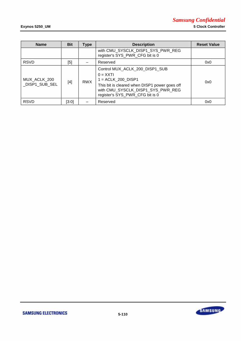
Samsung Confidential Exynos 5250_UM 5 Clock Controller
5-110
Name Bit Type Description Reset Value
with CMU_SYSCLK_DISP1_SYS_PWR_REG
register's SYS_PWR_CFG bit is 0
RSVD [5] – Reserved 0x0
MUX_ACLK_200
_DISP1_SUB_SEL [4] RWX
Control MUX_ACLK_200_DISP1_SUB
0 = XXTI
1 = ACLK_200_DISP1
This bit is cleared when DISP1 power goes off
with CMU_SYSCLK_DISP1_SYS_PWR_REG
register's SYS_PWR_CFG bit is 0
0x0
RSVD [3:0] – Reserved 0x0
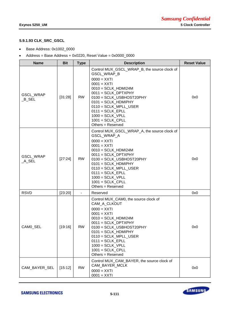
Samsung Confidential Exynos 5250_UM 5 Clock Controller
5-111
5.9.1.93 CLK_SRC_GSCL
Base Address: 0x1002_0000
Address = Base Address + 0x0220, Reset Value = 0x0000_0000
Name Bit Type Description Reset Value
GSCL_WRAP
_B_SEL [31:28] RW
Control MUX_GSCL_WRAP_B, the source clock of
GSCL_WRAP_B
0000 = XXTI
0001 = XXTI
0010 = SCLK_HDMI24M
0011 = SCLK_DPTXPHY
0100 = SCLK_USBHOST20PHY
0101 = SCLK_HDMIPHY
0110 = SCLK_MPLL_USER
0111 = SCLK_EPLL
1000 = SCLK_VPLL
1001 = SCLK_CPLL
Others = Reserved
0x0
GSCL_WRAP
_A_SEL [27:24] RW
Control MUX_GSCL_WRAP_A, the source clock of
GSCL_WRAP_A
0000 = XXTI
0001 = XXTI
0010 = SCLK_HDMI24M
0011 = SCLK_DPTXPHY
0100 = SCLK_USBHOST20PHY
0101 = SCLK_HDMIPHY
0110 = SCLK_MPLL_USER
0111 = SCLK_EPLL
1000 = SCLK_VPLL
1001 = SCLK_CPLL
Others = Reserved
0x0
RSVD [23:20] - Reserved 0x0
CAM0_SEL [19:16] RW
Control MUX_CAM0, the source clock of
CAM_A_CLKOUT
0000 = XXTI
0001 = XXTI
0010 = SCLK_HDMI24M
0011 = SCLK_DPTXPHY
0100 = SCLK_USBHOST20PHY
0101 = SCLK_HDMIPHY
0110 = SCLK_MPLL_USER
0111 = SCLK_EPLL
1000 = SCLK_VPLL
1001 = SCLK_CPLL
Others = Reserved
0x0
CAM_BAYER_SEL [15:12] RW
Control MUX_CAM_BAYER, the source clock of
CAM_BAYER_MCLK
0000 = XXTI
0001 = XXTI
0x0
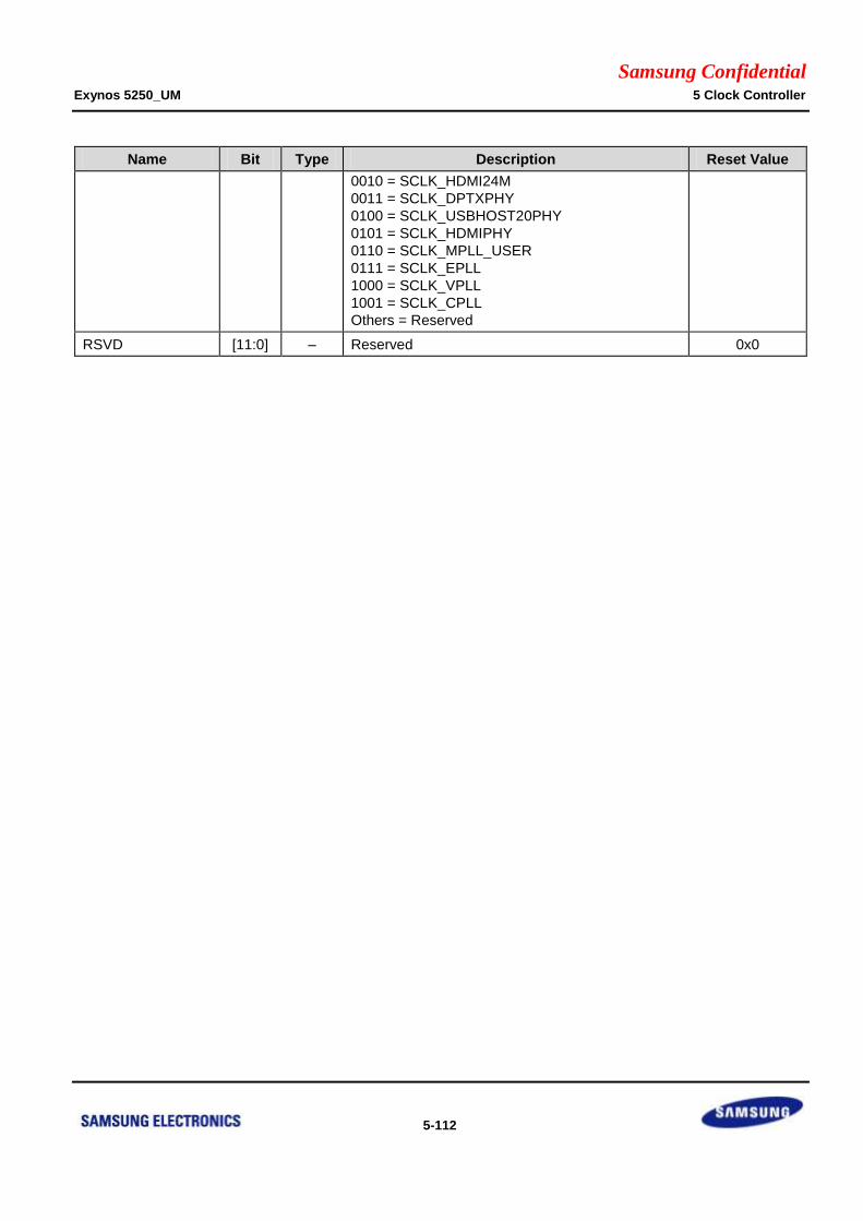
Samsung Confidential Exynos 5250_UM 5 Clock Controller
5-112
Name Bit Type Description Reset Value
0010 = SCLK_HDMI24M
0011 = SCLK_DPTXPHY
0100 = SCLK_USBHOST20PHY
0101 = SCLK_HDMIPHY
0110 = SCLK_MPLL_USER
0111 = SCLK_EPLL
1000 = SCLK_VPLL
1001 = SCLK_CPLL
Others = Reserved
RSVD [11:0] – Reserved 0x0

Samsung Confidential Exynos 5250_UM 5 Clock Controller
5-113
5.9.1.94 CLK_SRC_DISP1_0
Base Address: 0x1002_0000
Address = Base Address + 0x022C, Reset Value = 0x0000_0000
Name Bit Type Description Reset Value
RSVD [31:21] – Reserved 0x0
HDMI_SEL [20] RW
Control MUX_HDMI, the source clock of HDMI link
0 = SCLK_PIXEL
1 = SCLK_HDMIPHY
0x0
DP1_EXT_MST
_VID_SEL [19:16] RW
Control MUX_DP1_EXT_MST_VID, the source
clock of DP1_EXT_MST_VID
0000 = XXTI
0001 = XXTI
0010 = SCLK_HDMI24M
0011 = SCLK_DPTXPHY
0100 = SCLK_USBHOST20PHY
0101 = SCLK_HDMIPHY
0110 = SCLK_MPLL_USER
0111 = SCLK_EPLL
1000 = SCLK_VPLL
1001 = SCLK_CPLL
Others = Reserved
0x0
MIPI1_SEL [15:12] RW
Control MUX_MIPI1, the source clock of
MIPI_DSIM1
0000 = XXTI
0001 = XXTI
0010 = SCLK_HDMI24M
0011 = SCLK_DPTXPHY
0100 = SCLK_USBHOST20PHY
0101 = SCLK_HDMIPHY
0110 = SCLK_MPLL_USER
0111 = SCLK_EPLL
1000 = SCLK_VPLL
1001 = SCLK_CPLL
Others = Reserved
0x0
RSVD [11:4] – Reserved 0x0
FIMD1_SEL [3:0] RW
Control MUX_FIMD1, the source clock of FIMD1
0000 = XXTI
0001 = XXTI
0010 = SCLK_HDMI24M
0011 = SCLK_DPTXPHY
0100 = SCLK_USBHOST20PHY
0101 = SCLK_HDMIPHY
0110 = SCLK_MPLL_USER
0111 = SCLK_EPLL
1000 = SCLK_VPLL
1001 = SCLK_CPLL
Others = Reserved
0x0
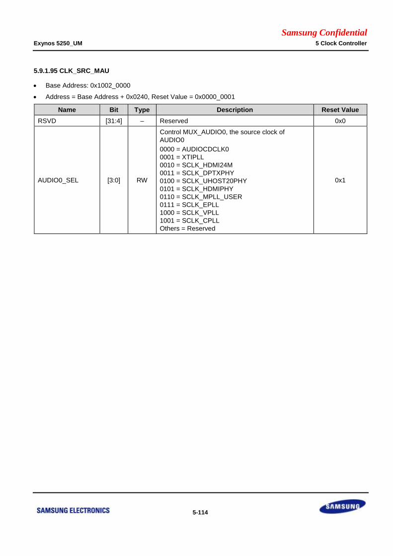
Samsung Confidential Exynos 5250_UM 5 Clock Controller
5-114
5.9.1.95 CLK_SRC_MAU
Base Address: 0x1002_0000
Address = Base Address + 0x0240, Reset Value = 0x0000_0001
Name Bit Type Description Reset Value
RSVD [31:4] – Reserved 0x0
AUDIO0_SEL [3:0] RW
Control MUX_AUDIO0, the source clock of
AUDIO0
0000 = AUDIOCDCLK0
0001 = XTIPLL
0010 = SCLK_HDMI24M
0011 = SCLK_DPTXPHY
0100 = SCLK_UHOST20PHY
0101 = SCLK_HDMIPHY
0110 = SCLK_MPLL_USER
0111 = SCLK_EPLL
1000 = SCLK_VPLL
1001 = SCLK_CPLL
Others = Reserved
0x1
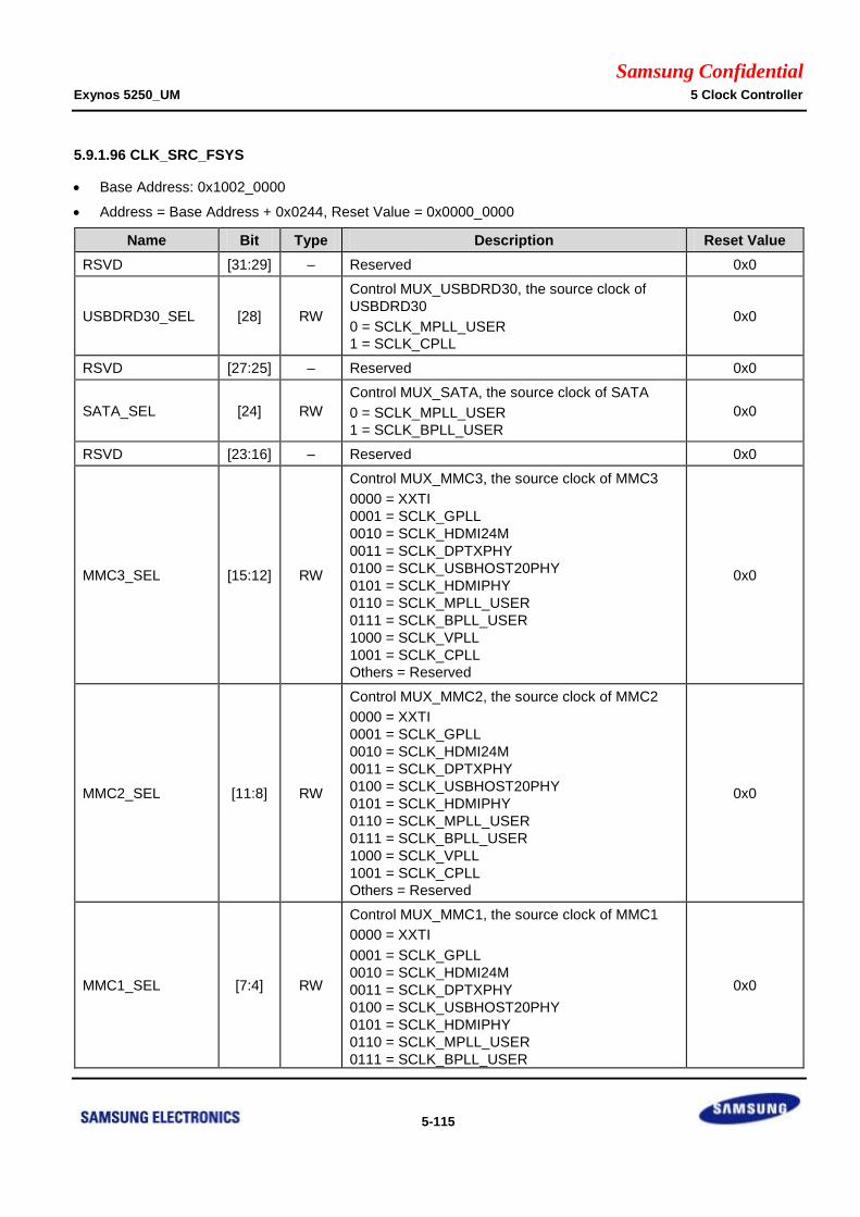
Samsung Confidential Exynos 5250_UM 5 Clock Controller
5-115
5.9.1.96 CLK_SRC_FSYS
Base Address: 0x1002_0000
Address = Base Address + 0x0244, Reset Value = 0x0000_0000
Name Bit Type Description Reset Value
RSVD [31:29] – Reserved 0x0
USBDRD30_SEL [28] RW
Control MUX_USBDRD30, the source clock of
USBDRD30
0 = SCLK_MPLL_USER
1 = SCLK_CPLL
0x0
RSVD [27:25] – Reserved 0x0
SATA_SEL [24] RW
Control MUX_SATA, the source clock of SATA
0 = SCLK_MPLL_USER
1 = SCLK_BPLL_USER
0x0
RSVD [23:16] – Reserved 0x0
MMC3_SEL [15:12] RW
Control MUX_MMC3, the source clock of MMC3
0000 = XXTI
0001 = SCLK_GPLL
0010 = SCLK_HDMI24M
0011 = SCLK_DPTXPHY
0100 = SCLK_USBHOST20PHY
0101 = SCLK_HDMIPHY
0110 = SCLK_MPLL_USER
0111 = SCLK_BPLL_USER
1000 = SCLK_VPLL
1001 = SCLK_CPLL
Others = Reserved
0x0
MMC2_SEL [11:8] RW
Control MUX_MMC2, the source clock of MMC2
0000 = XXTI
0001 = SCLK_GPLL
0010 = SCLK_HDMI24M
0011 = SCLK_DPTXPHY
0100 = SCLK_USBHOST20PHY
0101 = SCLK_HDMIPHY
0110 = SCLK_MPLL_USER
0111 = SCLK_BPLL_USER
1000 = SCLK_VPLL
1001 = SCLK_CPLL
Others = Reserved
0x0
MMC1_SEL [7:4] RW
Control MUX_MMC1, the source clock of MMC1
0000 = XXTI
0001 = SCLK_GPLL
0010 = SCLK_HDMI24M
0011 = SCLK_DPTXPHY
0100 = SCLK_USBHOST20PHY
0101 = SCLK_HDMIPHY
0110 = SCLK_MPLL_USER
0111 = SCLK_BPLL_USER
0x0

Samsung Confidential Exynos 5250_UM 5 Clock Controller
5-116
Name Bit Type Description Reset Value
1000 = SCLK_VPLL
1001 = SCLK_CPLL
Others = Reserved
MMC0_SEL [3:0] RW
Control MUX_MMC0, the source clock of MMC0
0000 = XXTI
0001 = SCLK_GPLL
0010 = SCLK_HDMI24M
0011 = SCLK_DPTXPHY
0100 = SCLK_USBHOST20PHY
0101 = SCLK_HDMIPHY
0110 = SCLK_MPLL_USER
0111 = SCLK_BPLL_USER
1000 = SCLK_VPLL
1001 = SCLK_CPLL
Others = Reserved
0x0
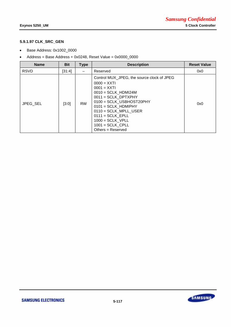
Samsung Confidential Exynos 5250_UM 5 Clock Controller
5-117
5.9.1.97 CLK_SRC_GEN
Base Address: 0x1002_0000
Address = Base Address + 0x0248, Reset Value = 0x0000_0000
Name Bit Type Description Reset Value
RSVD [31:4] – Reserved 0x0
JPEG_SEL [3:0] RW
Control MUX_JPEG, the source clock of JPEG
0000 = XXTI
0001 = XXTI
0010 = SCLK_HDMI24M
0011 = SCLK_DPTXPHY
0100 = SCLK_USBHOST20PHY
0101 = SCLK_HDMIPHY
0110 = SCLK_MPLL_USER
0111 = SCLK_EPLL
1000 = SCLK_VPLL
1001 = SCLK_CPLL
Others = Reserved
0x0
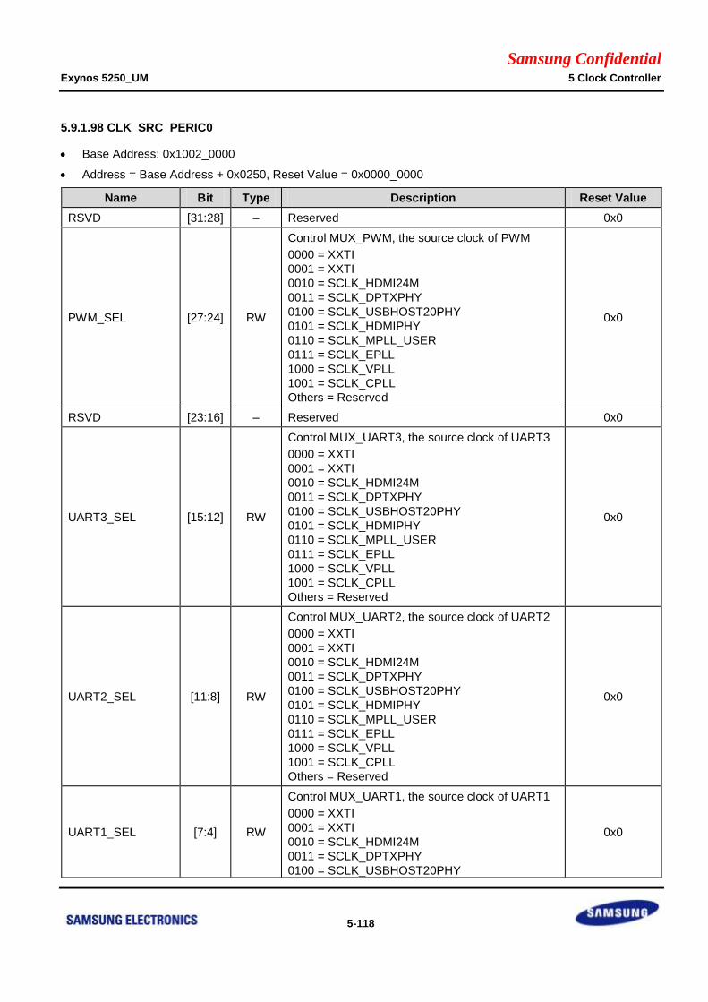
Samsung Confidential Exynos 5250_UM 5 Clock Controller
5-118
5.9.1.98 CLK_SRC_PERIC0
Base Address: 0x1002_0000
Address = Base Address + 0x0250, Reset Value = 0x0000_0000
Name Bit Type Description Reset Value
RSVD [31:28] – Reserved 0x0
PWM_SEL [27:24] RW
Control MUX_PWM, the source clock of PWM
0000 = XXTI
0001 = XXTI
0010 = SCLK_HDMI24M
0011 = SCLK_DPTXPHY
0100 = SCLK_USBHOST20PHY
0101 = SCLK_HDMIPHY
0110 = SCLK_MPLL_USER
0111 = SCLK_EPLL
1000 = SCLK_VPLL
1001 = SCLK_CPLL
Others = Reserved
0x0
RSVD [23:16] – Reserved 0x0
UART3_SEL [15:12] RW
Control MUX_UART3, the source clock of UART3
0000 = XXTI
0001 = XXTI
0010 = SCLK_HDMI24M
0011 = SCLK_DPTXPHY
0100 = SCLK_USBHOST20PHY
0101 = SCLK_HDMIPHY
0110 = SCLK_MPLL_USER
0111 = SCLK_EPLL
1000 = SCLK_VPLL
1001 = SCLK_CPLL
Others = Reserved
0x0
UART2_SEL [11:8] RW
Control MUX_UART2, the source clock of UART2
0000 = XXTI
0001 = XXTI
0010 = SCLK_HDMI24M
0011 = SCLK_DPTXPHY
0100 = SCLK_USBHOST20PHY
0101 = SCLK_HDMIPHY
0110 = SCLK_MPLL_USER
0111 = SCLK_EPLL
1000 = SCLK_VPLL
1001 = SCLK_CPLL
Others = Reserved
0x0
UART1_SEL [7:4] RW
Control MUX_UART1, the source clock of UART1
0000 = XXTI
0001 = XXTI
0010 = SCLK_HDMI24M
0011 = SCLK_DPTXPHY
0100 = SCLK_USBHOST20PHY
0x0

Samsung Confidential Exynos 5250_UM 5 Clock Controller
5-119
Name Bit Type Description Reset Value
0101 = SCLK_HDMIPHY
0110 = SCLK_MPLL_USER
0111 = SCLK_EPLL
1000 = SCLK_VPLL
1001 = SCLK_CPLL
Others = Reserved
UART0_SEL [3:0] RW
Control MUX_UART0, the source clock of UART0
0000 = XXTI
0001 = XXTI
0010 = SCLK_HDMI24M
0011 = SCLK_DPTXPHY
0100 = SCLK_USBHOST20PHY
0101 = SCLK_HDMIPHY
0110 = SCLK_MPLL_USER
0111 = SCLK_EPLL
1000 = SCLK_VPLL
1001 = SCLK_CPLL
Others = Reserved
0x0
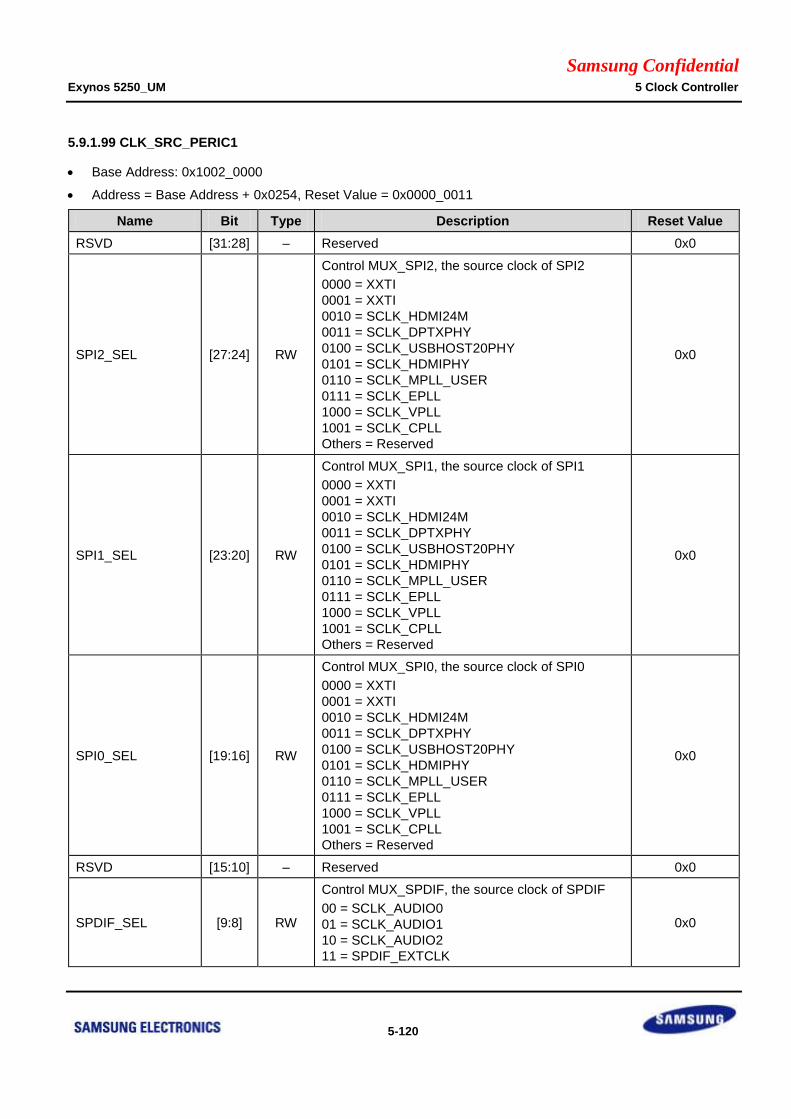
Samsung Confidential Exynos 5250_UM 5 Clock Controller
5-120
5.9.1.99 CLK_SRC_PERIC1
Base Address: 0x1002_0000
Address = Base Address + 0x0254, Reset Value = 0x0000_0011
Name Bit Type Description Reset Value
RSVD [31:28] – Reserved 0x0
SPI2_SEL [27:24] RW
Control MUX_SPI2, the source clock of SPI2
0000 = XXTI
0001 = XXTI
0010 = SCLK_HDMI24M
0011 = SCLK_DPTXPHY
0100 = SCLK_USBHOST20PHY
0101 = SCLK_HDMIPHY
0110 = SCLK_MPLL_USER
0111 = SCLK_EPLL
1000 = SCLK_VPLL
1001 = SCLK_CPLL
Others = Reserved
0x0
SPI1_SEL [23:20] RW
Control MUX_SPI1, the source clock of SPI1
0000 = XXTI
0001 = XXTI
0010 = SCLK_HDMI24M
0011 = SCLK_DPTXPHY
0100 = SCLK_USBHOST20PHY
0101 = SCLK_HDMIPHY
0110 = SCLK_MPLL_USER
0111 = SCLK_EPLL
1000 = SCLK_VPLL
1001 = SCLK_CPLL
Others = Reserved
0x0
SPI0_SEL [19:16] RW
Control MUX_SPI0, the source clock of SPI0
0000 = XXTI
0001 = XXTI
0010 = SCLK_HDMI24M
0011 = SCLK_DPTXPHY
0100 = SCLK_USBHOST20PHY
0101 = SCLK_HDMIPHY
0110 = SCLK_MPLL_USER
0111 = SCLK_EPLL
1000 = SCLK_VPLL
1001 = SCLK_CPLL
Others = Reserved
0x0
RSVD [15:10] – Reserved 0x0
SPDIF_SEL [9:8] RW
Control MUX_SPDIF, the source clock of SPDIF
00 = SCLK_AUDIO0
01 = SCLK_AUDIO1
10 = SCLK_AUDIO2
11 = SPDIF_EXTCLK
0x0
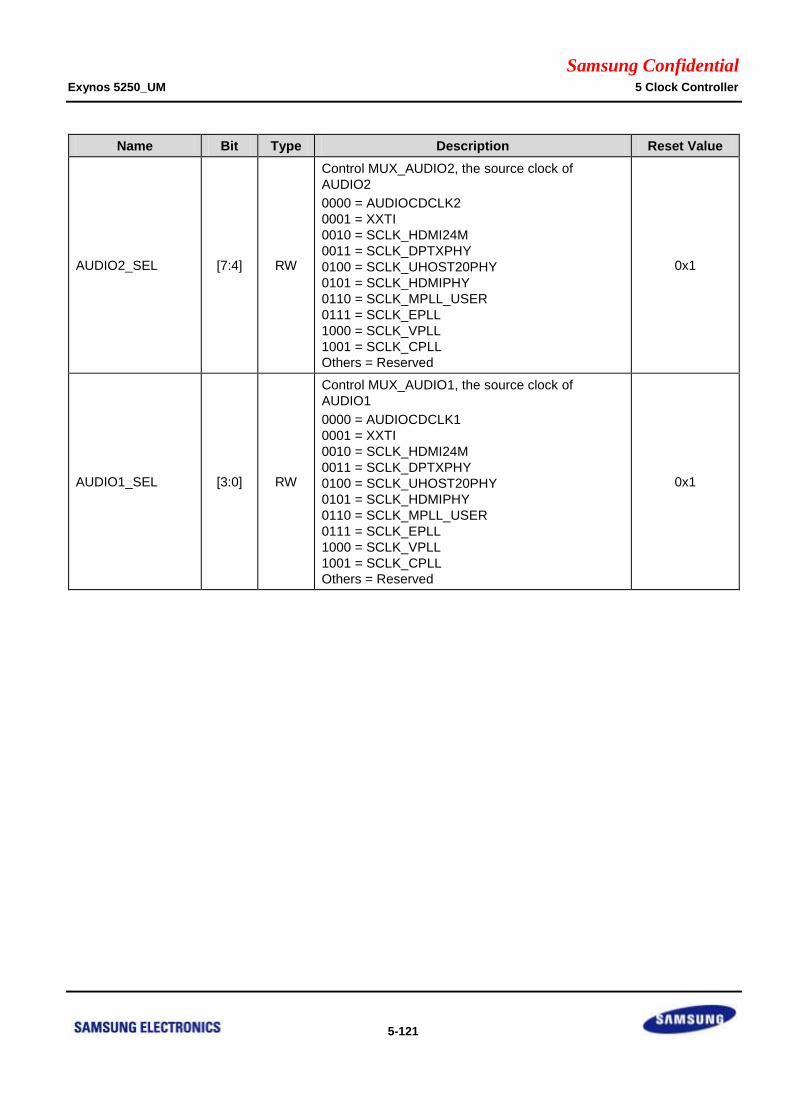
Samsung Confidential Exynos 5250_UM 5 Clock Controller
5-121
Name Bit Type Description Reset Value
AUDIO2_SEL [7:4] RW
Control MUX_AUDIO2, the source clock of
AUDIO2
0000 = AUDIOCDCLK2
0001 = XXTI
0010 = SCLK_HDMI24M
0011 = SCLK_DPTXPHY
0100 = SCLK_UHOST20PHY
0101 = SCLK_HDMIPHY
0110 = SCLK_MPLL_USER
0111 = SCLK_EPLL
1000 = SCLK_VPLL
1001 = SCLK_CPLL
Others = Reserved
0x1
AUDIO1_SEL [3:0] RW
Control MUX_AUDIO1, the source clock of
AUDIO1
0000 = AUDIOCDCLK1
0001 = XXTI
0010 = SCLK_HDMI24M
0011 = SCLK_DPTXPHY
0100 = SCLK_UHOST20PHY
0101 = SCLK_HDMIPHY
0110 = SCLK_MPLL_USER
0111 = SCLK_EPLL
1000 = SCLK_VPLL
1001 = SCLK_CPLL
Others = Reserved
0x1

Samsung Confidential Exynos 5250_UM 5 Clock Controller
5-122
5.9.1.100 SCLK_SRC_ISP
Base Address: 0x1002_0000
Address = Base Address + 0x0270, Reset Value = 0x0000_0000
Name Bit Type Description Reset Value
RSVD [31:16] – Reserved 0x0
PWM_ISP_SEL [15:12] RW
Control MUX_PWM_ISP, the source clock of
PWM_ISP
0000 = XXTI
0001 = XXTI
0010 = SCLK_HDMI24M
0011 = SCLK_DPTXPHY
0100 = SCLK_USBHOST20PHY
0101 = SCLK_HDMIPHY
0110 = SCLK_MPLL_USER
0111 = SCLK_EPLL
1000 = SCLK_VPLL
1001 = SCLK_CPLL
Others = Reserved
0x0
UART_ISP_SEL [11:8] RW
Control MUX_UART_ISP, the source clock of
UART_ISP
0000 = XXTI
0001 = XXTI
0010 = SCLK_HDMI24M
0011 = SCLK_DPTXPHY
0100 = SCLK_USBHOST20PHY
0101 = SCLK_HDMIPHY
0110 = SCLK_MPLL_USER
0111 = SCLK_EPLL
1000 = SCLK_VPLL
1001 = SCLK_CPLL
Others = Reserved
0x0
SPI1_ISP_SEL [7:4] RW
Control MUX_SPI1, the source clock of SPI1
0000 = XXTI
0001 = XXTI
0010 = SCLK_HDMI24M
0011 = SCLK_DPTXPHY
0100 = SCLK_USBHOST20PHY
0101 = SCLK_HDMIPHY
0110 = SCLK_MPLL_USER
0111 = SCLK_EPLL
1000 = SCLK_VPLL
1001 = SCLK_CPLL
Others = Reserved
0x0
SPI0_ISP_SEL [7:4] RW
Control MUX_SPI0, the source clock of SPI0
0000 = XXTI
0001 = XXTI
0010 = SCLK_HDMI24M
0011 = SCLK_DPTXPHY
0x0
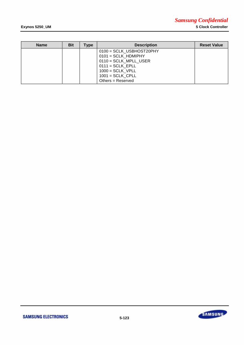
Samsung Confidential Exynos 5250_UM 5 Clock Controller
5-123
Name Bit Type Description Reset Value
0100 = SCLK_USBHOST20PHY
0101 = SCLK_HDMIPHY
0110 = SCLK_MPLL_USER
0111 = SCLK_EPLL
1000 = SCLK_VPLL
1001 = SCLK_CPLL
Others = Reserved
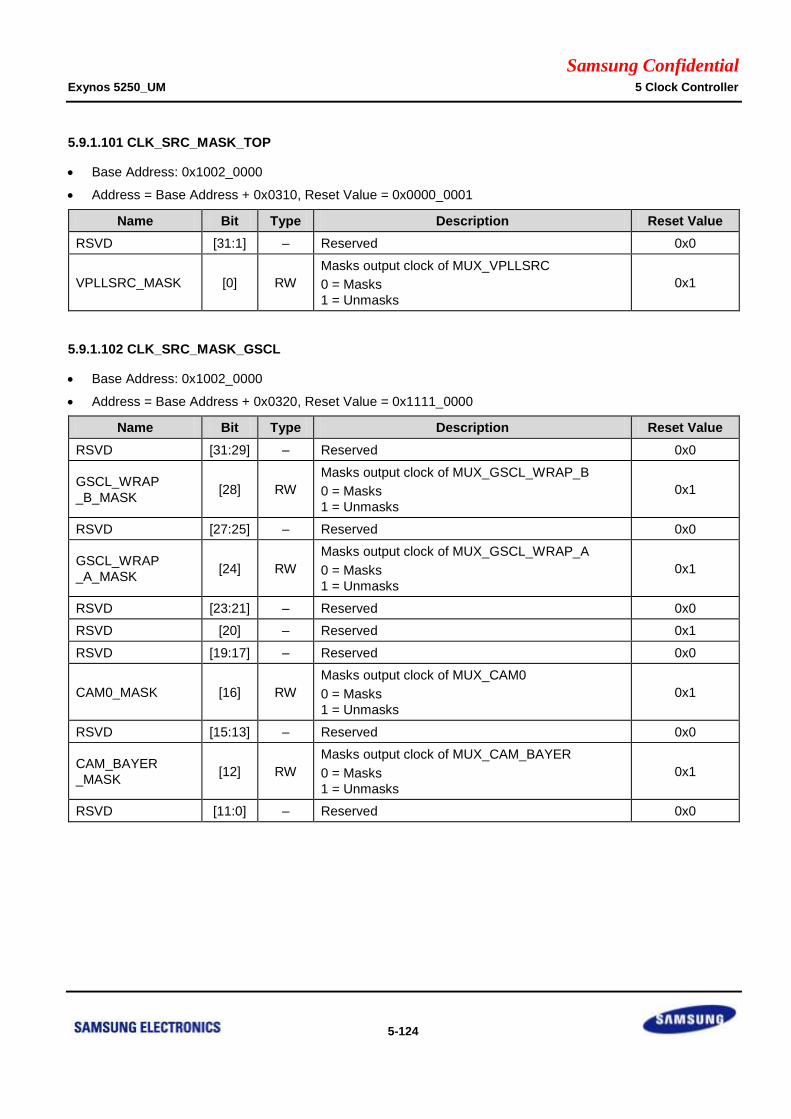
Samsung Confidential Exynos 5250_UM 5 Clock Controller
5-124
5.9.1.101 CLK_SRC_MASK_TOP
Base Address: 0x1002_0000
Address = Base Address + 0x0310, Reset Value = 0x0000_0001
Name Bit Type Description Reset Value
RSVD [31:1] – Reserved 0x0
VPLLSRC_MASK [0] RW
Masks output clock of MUX_VPLLSRC
0 = Masks
1 = Unmasks
0x1
5.9.1.102 CLK_SRC_MASK_GSCL
Base Address: 0x1002_0000
Address = Base Address + 0x0320, Reset Value = 0x1111_0000
Name Bit Type Description Reset Value
RSVD [31:29] – Reserved 0x0
GSCL_WRAP
_B_MASK [28] RW
Masks output clock of MUX_GSCL_WRAP_B
0 = Masks
1 = Unmasks
0x1
RSVD [27:25] – Reserved 0x0
GSCL_WRAP
_A_MASK [24] RW
Masks output clock of MUX_GSCL_WRAP_A
0 = Masks
1 = Unmasks
0x1
RSVD [23:21] – Reserved 0x0
RSVD [20] – Reserved 0x1
RSVD [19:17] – Reserved 0x0
CAM0_MASK [16] RW
Masks output clock of MUX_CAM0
0 = Masks
1 = Unmasks
0x1
RSVD [15:13] – Reserved 0x0
CAM_BAYER
_MASK [12] RW
Masks output clock of MUX_CAM_BAYER
0 = Masks
1 = Unmasks
0x1
RSVD [11:0] – Reserved 0x0
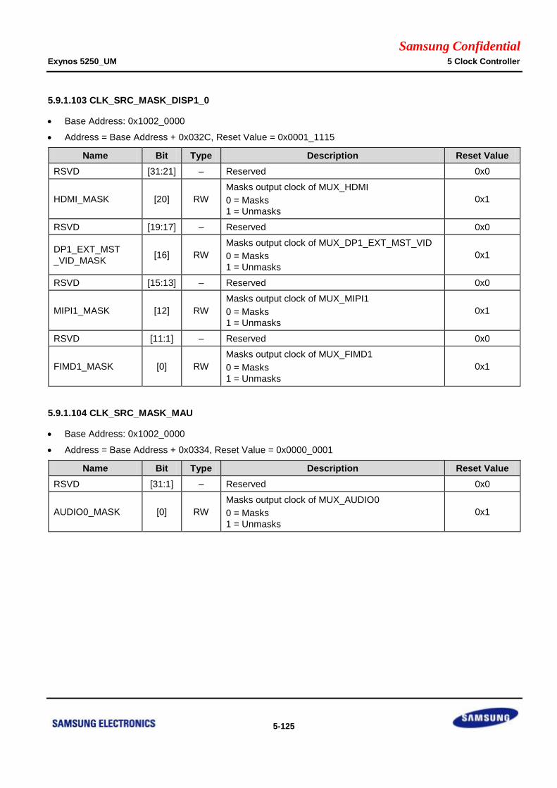
Samsung Confidential Exynos 5250_UM 5 Clock Controller
5-125
5.9.1.103 CLK_SRC_MASK_DISP1_0
Base Address: 0x1002_0000
Address = Base Address + 0x032C, Reset Value = 0x0001_1115
Name Bit Type Description Reset Value
RSVD [31:21] – Reserved 0x0
HDMI_MASK [20] RW
Masks output clock of MUX_HDMI
0 = Masks
1 = Unmasks
0x1
RSVD [19:17] – Reserved 0x0
DP1_EXT_MST
_VID_MASK [16] RW
Masks output clock of MUX_DP1_EXT_MST_VID
0 = Masks
1 = Unmasks
0x1
RSVD [15:13] – Reserved 0x0
MIPI1_MASK [12] RW
Masks output clock of MUX_MIPI1
0 = Masks
1 = Unmasks
0x1
RSVD [11:1] – Reserved 0x0
FIMD1_MASK [0] RW
Masks output clock of MUX_FIMD1
0 = Masks
1 = Unmasks
0x1
5.9.1.104 CLK_SRC_MASK_MAU
Base Address: 0x1002_0000
Address = Base Address + 0x0334, Reset Value = 0x0000_0001
Name Bit Type Description Reset Value
RSVD [31:1] – Reserved 0x0
AUDIO0_MASK [0] RW
Masks output clock of MUX_AUDIO0
0 = Masks
1 = Unmasks
0x1
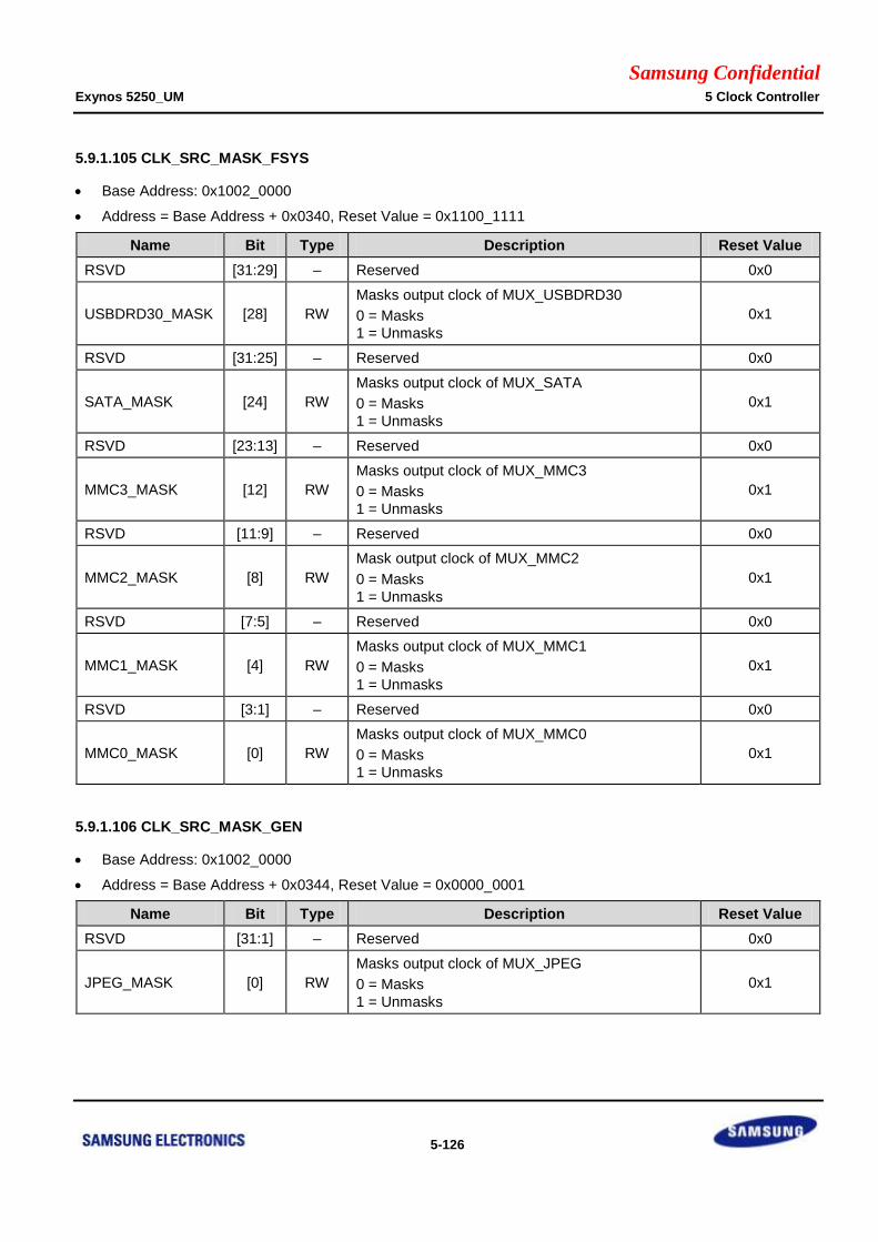
Samsung Confidential Exynos 5250_UM 5 Clock Controller
5-126
5.9.1.105 CLK_SRC_MASK_FSYS
Base Address: 0x1002_0000
Address = Base Address + 0x0340, Reset Value = 0x1100_1111
Name Bit Type Description Reset Value
RSVD [31:29] – Reserved 0x0
USBDRD30_MASK [28] RW
Masks output clock of MUX_USBDRD30
0 = Masks
1 = Unmasks
0x1
RSVD [31:25] – Reserved 0x0
SATA_MASK [24] RW
Masks output clock of MUX_SATA
0 = Masks
1 = Unmasks
0x1
RSVD [23:13] – Reserved 0x0
MMC3_MASK [12] RW
Masks output clock of MUX_MMC3
0 = Masks
1 = Unmasks
0x1
RSVD [11:9] – Reserved 0x0
MMC2_MASK [8] RW
Mask output clock of MUX_MMC2
0 = Masks
1 = Unmasks
0x1
RSVD [7:5] – Reserved 0x0
MMC1_MASK [4] RW
Masks output clock of MUX_MMC1
0 = Masks
1 = Unmasks
0x1
RSVD [3:1] – Reserved 0x0
MMC0_MASK [0] RW
Masks output clock of MUX_MMC0
0 = Masks
1 = Unmasks
0x1
5.9.1.106 CLK_SRC_MASK_GEN
Base Address: 0x1002_0000
Address = Base Address + 0x0344, Reset Value = 0x0000_0001
Name Bit Type Description Reset Value
RSVD [31:1] – Reserved 0x0
JPEG_MASK [0] RW
Masks output clock of MUX_JPEG
0 = Masks
1 = Unmasks
0x1
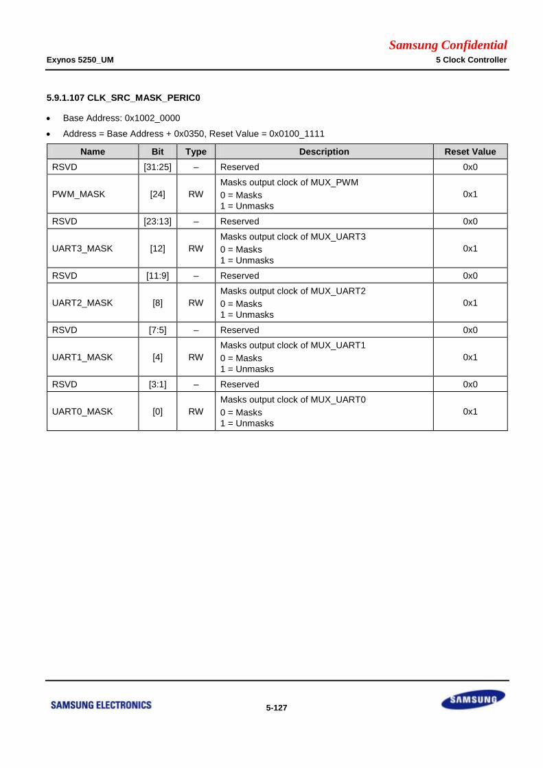
Samsung Confidential Exynos 5250_UM 5 Clock Controller
5-127
5.9.1.107 CLK_SRC_MASK_PERIC0
Base Address: 0x1002_0000
Address = Base Address + 0x0350, Reset Value = 0x0100_1111
Name Bit Type Description Reset Value
RSVD [31:25] – Reserved 0x0
PWM_MASK [24] RW
Masks output clock of MUX_PWM
0 = Masks
1 = Unmasks
0x1
RSVD [23:13] – Reserved 0x0
UART3_MASK [12] RW
Masks output clock of MUX_UART3
0 = Masks
1 = Unmasks
0x1
RSVD [11:9] – Reserved 0x0
UART2_MASK [8] RW
Masks output clock of MUX_UART2
0 = Masks
1 = Unmasks
0x1
RSVD [7:5] – Reserved 0x0
UART1_MASK [4] RW
Masks output clock of MUX_UART1
0 = Masks
1 = Unmasks
0x1
RSVD [3:1] – Reserved 0x0
UART0_MASK [0] RW
Masks output clock of MUX_UART0
0 = Masks
1 = Unmasks
0x1
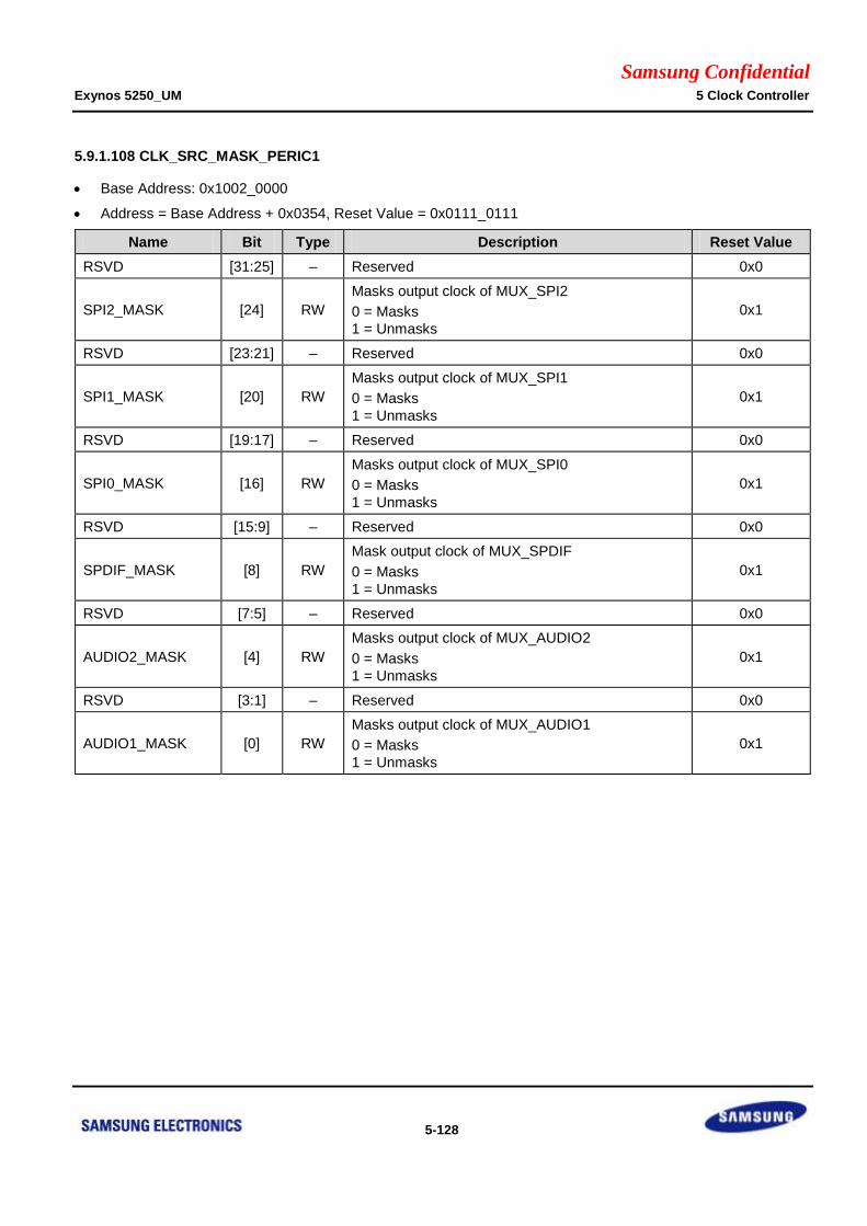
Samsung Confidential Exynos 5250_UM 5 Clock Controller
5-128
5.9.1.108 CLK_SRC_MASK_PERIC1
Base Address: 0x1002_0000
Address = Base Address + 0x0354, Reset Value = 0x0111_0111
Name Bit Type Description Reset Value
RSVD [31:25] – Reserved 0x0
SPI2_MASK [24] RW
Masks output clock of MUX_SPI2
0 = Masks
1 = Unmasks
0x1
RSVD [23:21] – Reserved 0x0
SPI1_MASK [20] RW
Masks output clock of MUX_SPI1
0 = Masks
1 = Unmasks
0x1
RSVD [19:17] – Reserved 0x0
SPI0_MASK [16] RW
Masks output clock of MUX_SPI0
0 = Masks
1 = Unmasks
0x1
RSVD [15:9] – Reserved 0x0
SPDIF_MASK [8] RW
Mask output clock of MUX_SPDIF
0 = Masks
1 = Unmasks
0x1
RSVD [7:5] – Reserved 0x0
AUDIO2_MASK [4] RW
Masks output clock of MUX_AUDIO2
0 = Masks
1 = Unmasks
0x1
RSVD [3:1] – Reserved 0x0
AUDIO1_MASK [0] RW
Masks output clock of MUX_AUDIO1
0 = Masks
1 = Unmasks
0x1
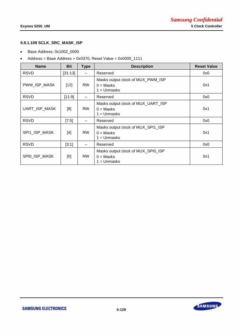
Samsung Confidential Exynos 5250_UM 5 Clock Controller
5-129
5.9.1.109 SCLK_SRC_MASK_ISP
Base Address: 0x1002_0000
Address = Base Address + 0x0370, Reset Value = 0x0000_1111
Name Bit Type Description Reset Value
RSVD [31:13] – Reserved 0x0
PWM_ISP_MASK [12] RW
Masks output clock of MUX_PWM_ISP
0 = Masks
1 = Unmasks
0x1
RSVD [11:9] – Reserved 0x0
UART_ISP_MASK [8] RW
Masks output clock of MUX_UART_ISP
0 = Masks
1 = Unmasks
0x1
RSVD [7:5] – Reserved 0x0
SPI1_ISP_MASK [4] RW
Masks output clock of MUX_SPI1_ISP
0 = Masks
1 = Unmasks
0x1
RSVD [3:1] – Reserved 0x0
SPI0_ISP_MASK [0] RW
Masks output clock of MUX_SPI0_ISP
0 = Masks
1 = Unmasks
0x1
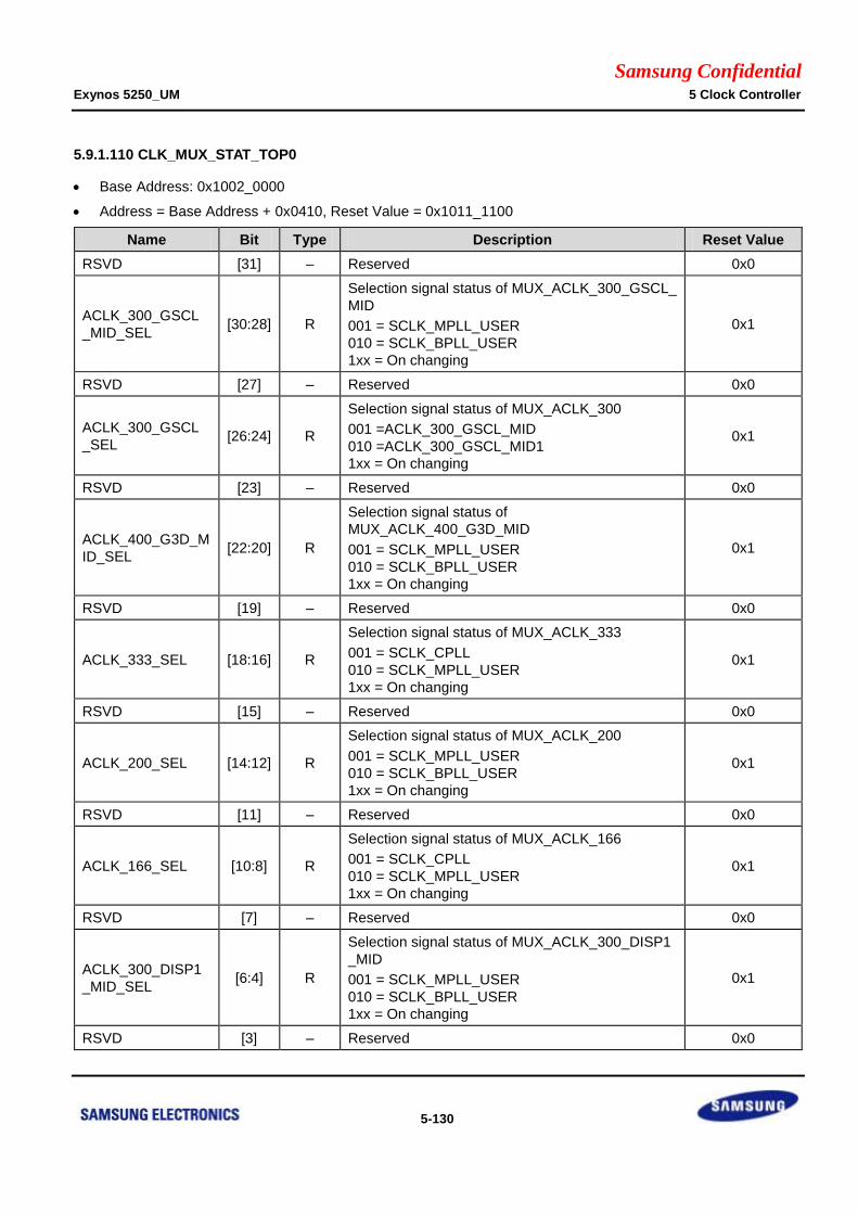
Samsung Confidential Exynos 5250_UM 5 Clock Controller
5-130
5.9.1.110 CLK_MUX_STAT_TOP0
Base Address: 0x1002_0000
Address = Base Address + 0x0410, Reset Value = 0x1011_1100
Name Bit Type Description Reset Value
RSVD [31] – Reserved 0x0
ACLK_300_GSCL
_MID_SEL [30:28] R
Selection signal status of MUX_ACLK_300_GSCL_
MID
001 = SCLK_MPLL_USER
010 = SCLK_BPLL_USER
1xx = On changing
0x1
RSVD [27] – Reserved 0x0
ACLK_300_GSCL
_SEL [26:24] R
Selection signal status of MUX_ACLK_300
001 =ACLK_300_GSCL_MID
010 =ACLK_300_GSCL_MID1
1xx = On changing
0x1
RSVD [23] – Reserved 0x0
ACLK_400_G3D_M
ID_SEL [22:20] R
Selection signal status of
MUX_ACLK_400_G3D_MID
001 = SCLK_MPLL_USER
010 = SCLK_BPLL_USER
1xx = On changing
0x1
RSVD [19] – Reserved 0x0
ACLK_333_SEL [18:16] R
Selection signal status of MUX_ACLK_333
001 = SCLK_CPLL
010 = SCLK_MPLL_USER
1xx = On changing
0x1
RSVD [15] – Reserved 0x0
ACLK_200_SEL [14:12] R
Selection signal status of MUX_ACLK_200
001 = SCLK_MPLL_USER
010 = SCLK_BPLL_USER
1xx = On changing
0x1
RSVD [11] – Reserved 0x0
ACLK_166_SEL [10:8] R
Selection signal status of MUX_ACLK_166
001 = SCLK_CPLL
010 = SCLK_MPLL_USER
1xx = On changing
0x1
RSVD [7] – Reserved 0x0
ACLK_300_DISP1
_MID_SEL [6:4] R
Selection signal status of MUX_ACLK_300_DISP1
_MID
001 = SCLK_MPLL_USER
010 = SCLK_BPLL_USER
1xx = On changing
0x1
RSVD [3] – Reserved 0x0
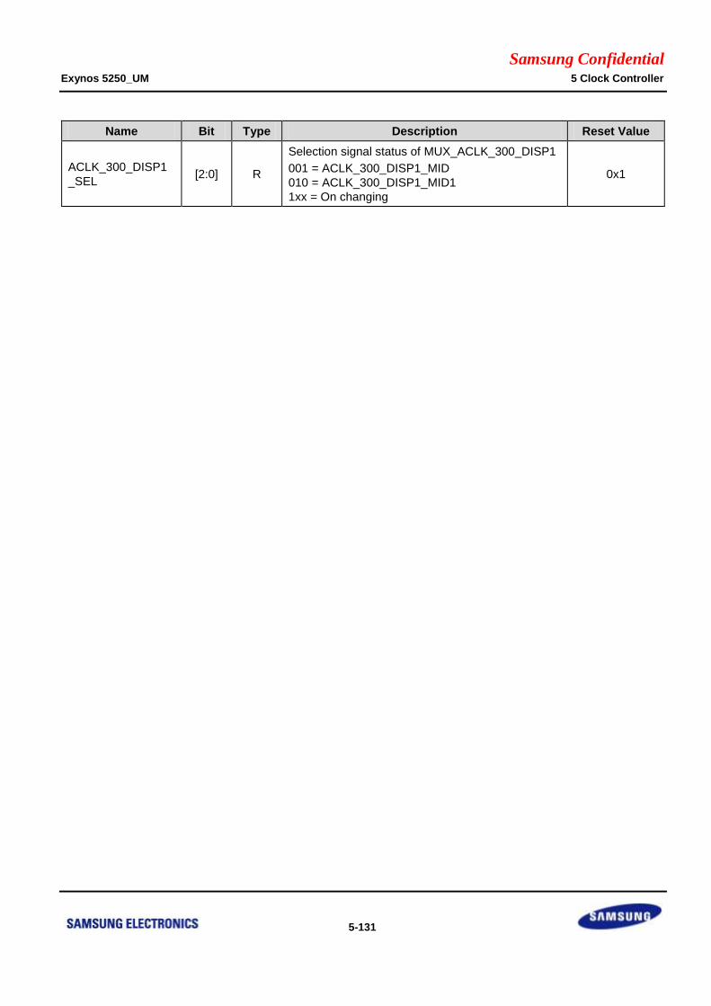
Samsung Confidential Exynos 5250_UM 5 Clock Controller
5-131
Name Bit Type Description Reset Value
ACLK_300_DISP1
_SEL [2:0] R
Selection signal status of MUX_ACLK_300_DISP1
001 = ACLK_300_DISP1_MID
010 = ACLK_300_DISP1_MID1
1xx = On changing
0x1
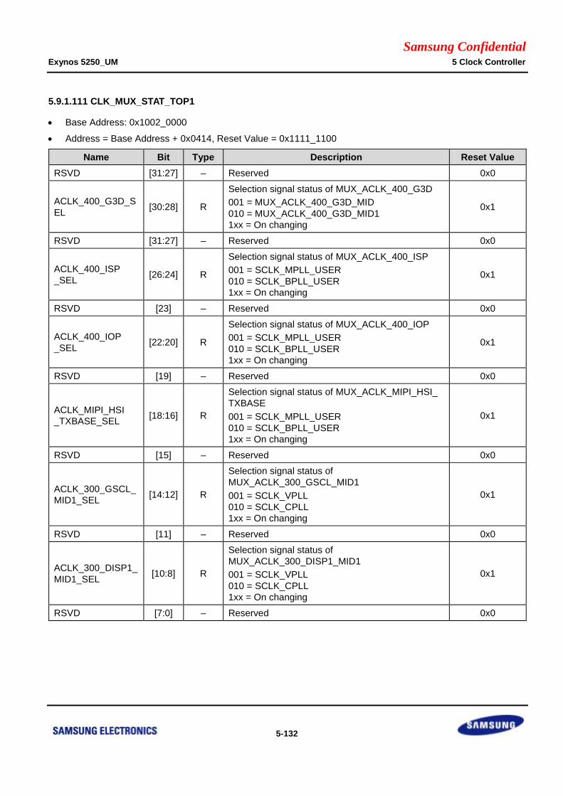
Samsung Confidential Exynos 5250_UM 5 Clock Controller
5-132
5.9.1.111 CLK_MUX_STAT_TOP1
Base Address: 0x1002_0000
Address = Base Address + 0x0414, Reset Value = 0x1111_1100
Name Bit Type Description Reset Value
RSVD [31:27] – Reserved 0x0
ACLK_400_G3D_S
EL [30:28] R
Selection signal status of MUX_ACLK_400_G3D
001 = MUX_ACLK_400_G3D_MID
010 = MUX_ACLK_400_G3D_MID1
1xx = On changing
0x1
RSVD [31:27] – Reserved 0x0
ACLK_400_ISP
_SEL [26:24] R
Selection signal status of MUX_ACLK_400_ISP
001 = SCLK_MPLL_USER
010 = SCLK_BPLL_USER
1xx = On changing
0x1
RSVD [23] – Reserved 0x0
ACLK_400_IOP
_SEL [22:20] R
Selection signal status of MUX_ACLK_400_IOP
001 = SCLK_MPLL_USER
010 = SCLK_BPLL_USER
1xx = On changing
0x1
RSVD [19] – Reserved 0x0
ACLK_MIPI_HSI
_TXBASE_SEL [18:16] R
Selection signal status of MUX_ACLK_MIPI_HSI_
TXBASE
001 = SCLK_MPLL_USER
010 = SCLK_BPLL_USER
1xx = On changing
0x1
RSVD [15] – Reserved 0x0
ACLK_300_GSCL_
MID1_SEL [14:12] R
Selection signal status of
MUX_ACLK_300_GSCL_MID1
001 = SCLK_VPLL
010 = SCLK_CPLL
1xx = On changing
0x1
RSVD [11] – Reserved 0x0
ACLK_300_DISP1_
MID1_SEL [10:8] R
Selection signal status of
MUX_ACLK_300_DISP1_MID1
001 = SCLK_VPLL
010 = SCLK_CPLL
1xx = On changing
0x1
RSVD [7:0] – Reserved 0x0
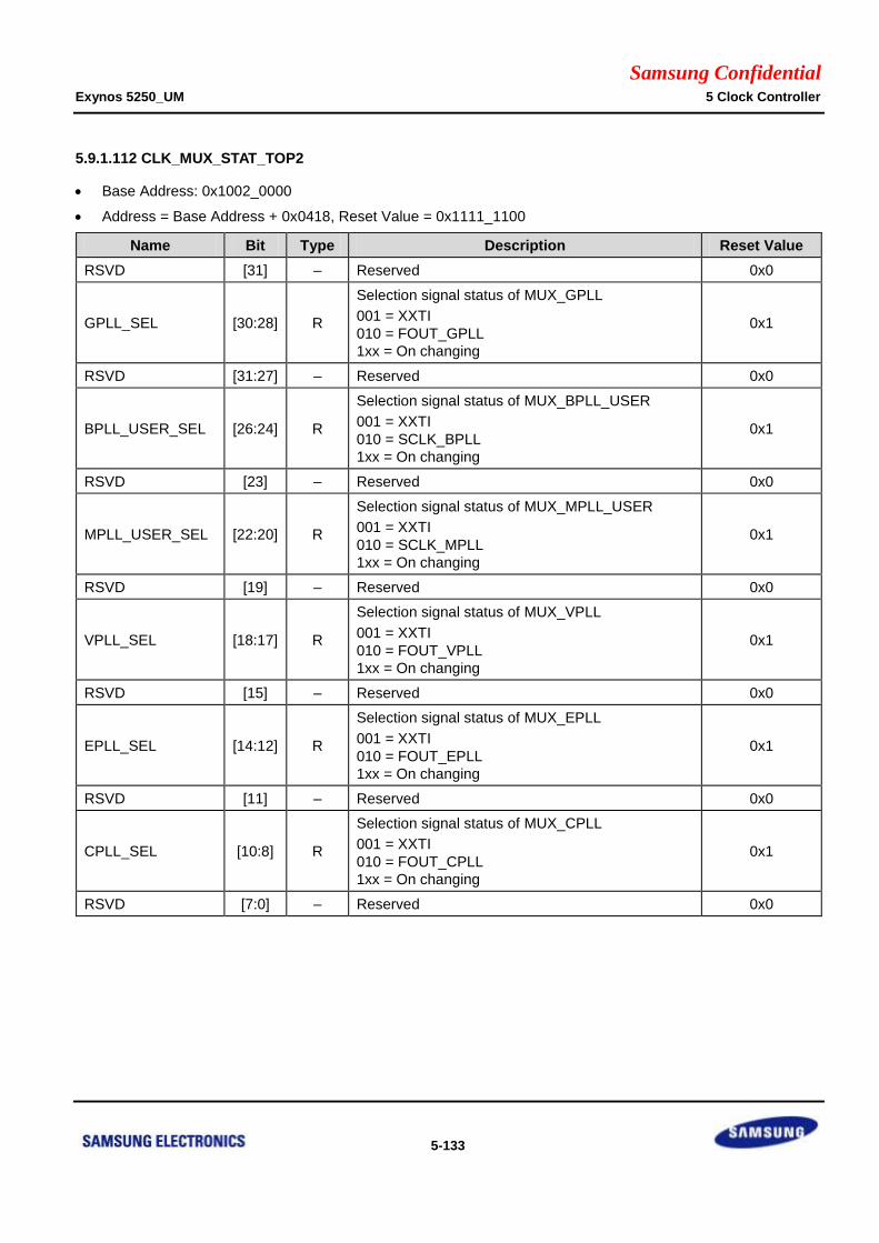
Samsung Confidential Exynos 5250_UM 5 Clock Controller
5-133
5.9.1.112 CLK_MUX_STAT_TOP2
Base Address: 0x1002_0000
Address = Base Address + 0x0418, Reset Value = 0x1111_1100
Name Bit Type Description Reset Value
RSVD [31] – Reserved 0x0
GPLL_SEL [30:28] R
Selection signal status of MUX_GPLL
001 = XXTI
010 = FOUT_GPLL
1xx = On changing
0x1
RSVD [31:27] – Reserved 0x0
BPLL_USER_SEL [26:24] R
Selection signal status of MUX_BPLL_USER
001 = XXTI
010 = SCLK_BPLL
1xx = On changing
0x1
RSVD [23] – Reserved 0x0
MPLL_USER_SEL [22:20] R
Selection signal status of MUX_MPLL_USER
001 = XXTI
010 = SCLK_MPLL
1xx = On changing
0x1
RSVD [19] – Reserved 0x0
VPLL_SEL [18:17] R
Selection signal status of MUX_VPLL
001 = XXTI
010 = FOUT_VPLL
1xx = On changing
0x1
RSVD [15] – Reserved 0x0
EPLL_SEL [14:12] R
Selection signal status of MUX_EPLL
001 = XXTI
010 = FOUT_EPLL
1xx = On changing
0x1
RSVD [11] – Reserved 0x0
CPLL_SEL [10:8] R
Selection signal status of MUX_CPLL
001 = XXTI
010 = FOUT_CPLL
1xx = On changing
0x1
RSVD [7:0] – Reserved 0x0
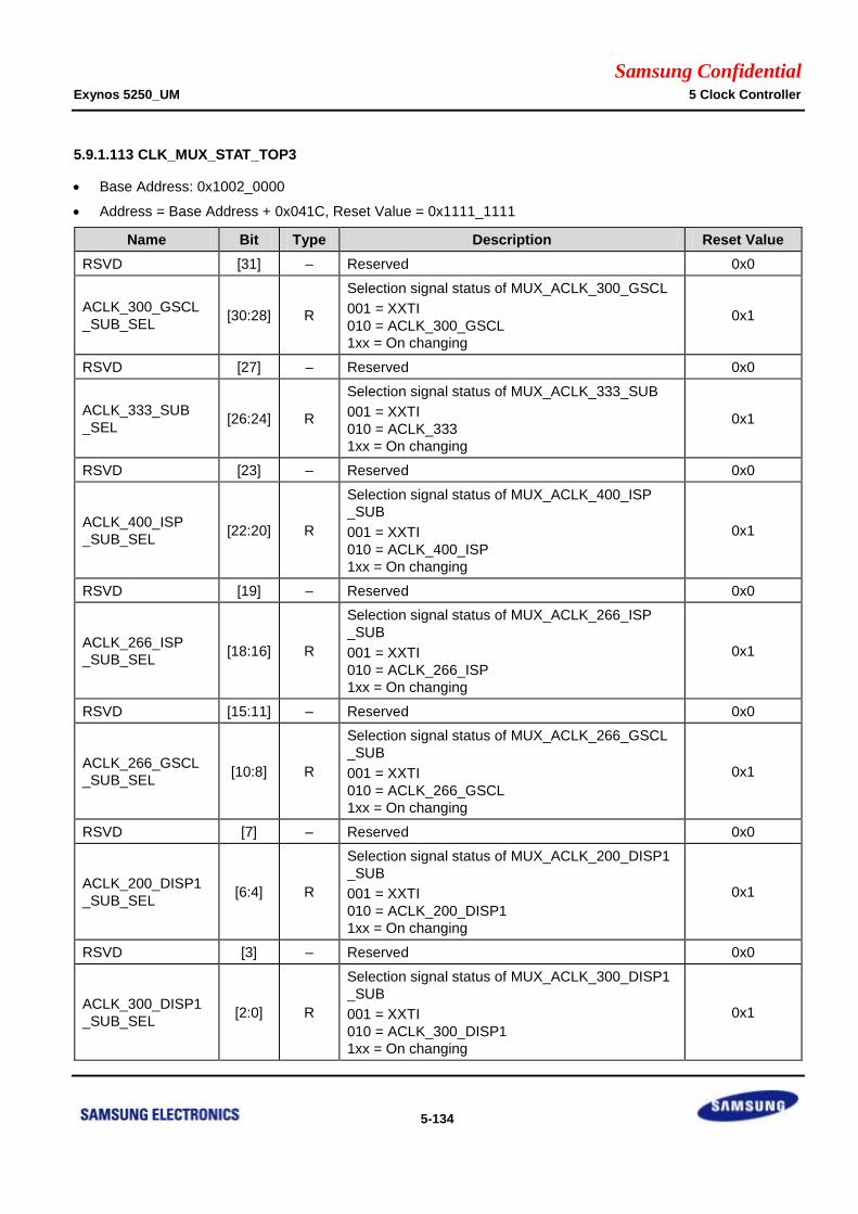
Samsung Confidential Exynos 5250_UM 5 Clock Controller
5-134
5.9.1.113 CLK_MUX_STAT_TOP3
Base Address: 0x1002_0000
Address = Base Address + 0x041C, Reset Value = 0x1111_1111
Name Bit Type Description Reset Value
RSVD [31] – Reserved 0x0
ACLK_300_GSCL
_SUB_SEL [30:28] R
Selection signal status of MUX_ACLK_300_GSCL
001 = XXTI
010 = ACLK_300_GSCL
1xx = On changing
0x1
RSVD [27] – Reserved 0x0
ACLK_333_SUB
_SEL [26:24] R
Selection signal status of MUX_ACLK_333_SUB
001 = XXTI
010 = ACLK_333
1xx = On changing
0x1
RSVD [23] – Reserved 0x0
ACLK_400_ISP
_SUB_SEL [22:20] R
Selection signal status of MUX_ACLK_400_ISP
_SUB
001 = XXTI
010 = ACLK_400_ISP
1xx = On changing
0x1
RSVD [19] – Reserved 0x0
ACLK_266_ISP
_SUB_SEL [18:16] R
Selection signal status of MUX_ACLK_266_ISP
_SUB
001 = XXTI
010 = ACLK_266_ISP
1xx = On changing
0x1
RSVD [15:11] – Reserved 0x0
ACLK_266_GSCL
_SUB_SEL [10:8] R
Selection signal status of MUX_ACLK_266_GSCL
_SUB
001 = XXTI
010 = ACLK_266_GSCL
1xx = On changing
0x1
RSVD [7] – Reserved 0x0
ACLK_200_DISP1
_SUB_SEL [6:4] R
Selection signal status of MUX_ACLK_200_DISP1
_SUB
001 = XXTI
010 = ACLK_200_DISP1
1xx = On changing
0x1
RSVD [3] – Reserved 0x0
ACLK_300_DISP1
_SUB_SEL [2:0] R
Selection signal status of MUX_ACLK_300_DISP1
_SUB
001 = XXTI
010 = ACLK_300_DISP1
1xx = On changing
0x1

Samsung Confidential Exynos 5250_UM 5 Clock Controller
5-135
5.9.1.114 CLK_DIV_TOP0
Base Address: 0x1002_0000
Address = Base Address + 0x0510, Reset Value = 0x0000_0000
Name Bit Type Description Reset Value
RSVD [31] – Reserved 0x0
ACLK_300_DISP1_
RATIO [30:28] RW
DIV_ACLK_300_DISP1 clock divider Ratio
ACLK_300_DISP1
=
MOUT_ACLK_300_DISP1/(ACLK_300_DISP1_RA
TIO + 1)
0x0
RSVD [27] – Reserved 0x0
ACLK_400_G3D_R
ATIO [26:24] RW
DIV_ACLK_400_G3D clock divider Ratio
ACLK_400_G3D
=
MOUT_ACLK_400_G3D/(ACLK_400_G3D_RATIO
+ 1)
0x0
RSVD [23] – Reserved 0x0
ACLK_333_RATIO [22:20] RW
DIV_ACLK_333 clock divider Ratio
ACLK_333
= MOUT_ACLK_333/(ACLK_333_RATIO + 1)
0x0
RSVD [19] – Reserved 0x0
ACLK_266_RATIO [18:16] RW
DIV_ACLK_266 clock divider Ratio
ACLK_266
= MOUT_MPLL_USER/(ACLK_266_RATIO + 1)
0x0
RSVD [15] – Reserved 0x0
ACLK_200_RATIO [14:12] RW
DIV_ACLK_200 clock divider Ratio
ACLK_200
= MOUT_ACLK_200/(ACLK_200_RATIO + 1)
0x0
RSVD [11] – Reserved 0x0
ACLK_166_RATIO [10:8] RW
DIV_ACLK_166 clock divider Ratio
ACLK166
= MOUT_ACLK_166/(ACLK_166_RATIO + 1)
0x0
RSVD [7:3] – Reserved 0x0
ACLK_66_RATIO [2:0] RW
DIV_ACLK_66 clock divider Ratio
ACLK_66
= DOUT_ACLK_66_PRE/(ACLK_66_RATIO + 1)
0x0
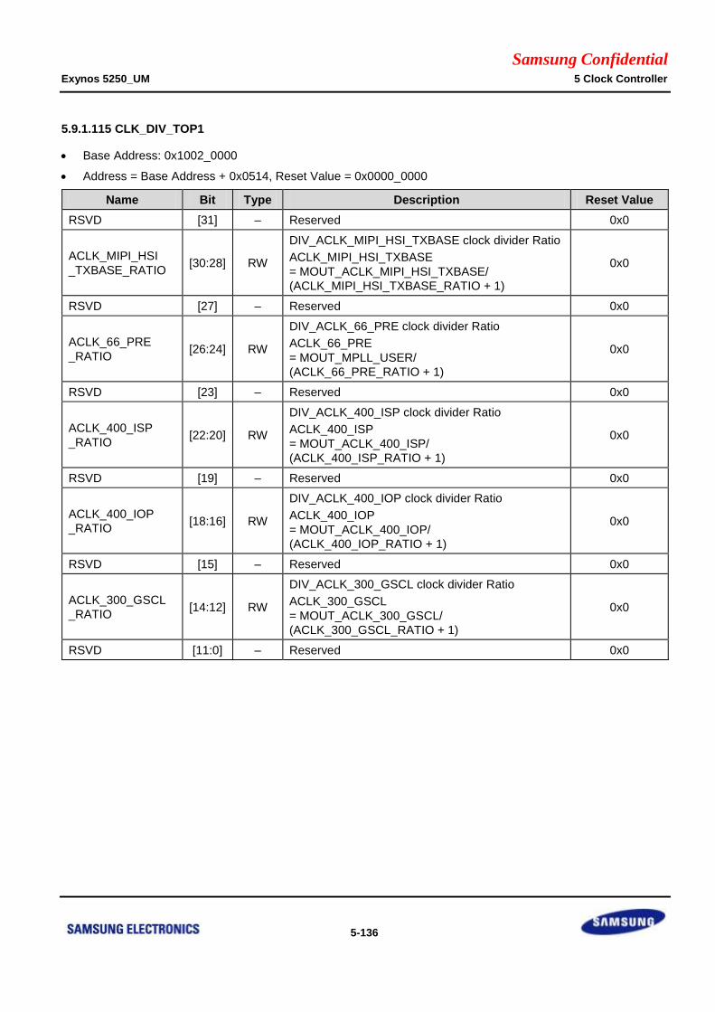
Samsung Confidential Exynos 5250_UM 5 Clock Controller
5-136
5.9.1.115 CLK_DIV_TOP1
Base Address: 0x1002_0000
Address = Base Address + 0x0514, Reset Value = 0x0000_0000
Name Bit Type Description Reset Value
RSVD [31] – Reserved 0x0
ACLK_MIPI_HSI
_TXBASE_RATIO [30:28] RW
DIV_ACLK_MIPI_HSI_TXBASE clock divider Ratio
ACLK_MIPI_HSI_TXBASE
= MOUT_ACLK_MIPI_HSI_TXBASE/
(ACLK_MIPI_HSI_TXBASE_RATIO + 1)
0x0
RSVD [27] – Reserved 0x0
ACLK_66_PRE
_RATIO [26:24] RW
DIV_ACLK_66_PRE clock divider Ratio
ACLK_66_PRE
= MOUT_MPLL_USER/
(ACLK_66_PRE_RATIO + 1)
0x0
RSVD [23] – Reserved 0x0
ACLK_400_ISP
_RATIO [22:20] RW
DIV_ACLK_400_ISP clock divider Ratio
ACLK_400_ISP
= MOUT_ACLK_400_ISP/
(ACLK_400_ISP_RATIO + 1)
0x0
RSVD [19] – Reserved 0x0
ACLK_400_IOP
_RATIO [18:16] RW
DIV_ACLK_400_IOP clock divider Ratio
ACLK_400_IOP
= MOUT_ACLK_400_IOP/
(ACLK_400_IOP_RATIO + 1)
0x0
RSVD [15] – Reserved 0x0
ACLK_300_GSCL
_RATIO [14:12] RW
DIV_ACLK_300_GSCL clock divider Ratio
ACLK_300_GSCL
= MOUT_ACLK_300_GSCL/
(ACLK_300_GSCL_RATIO + 1)
0x0
RSVD [11:0] – Reserved 0x0
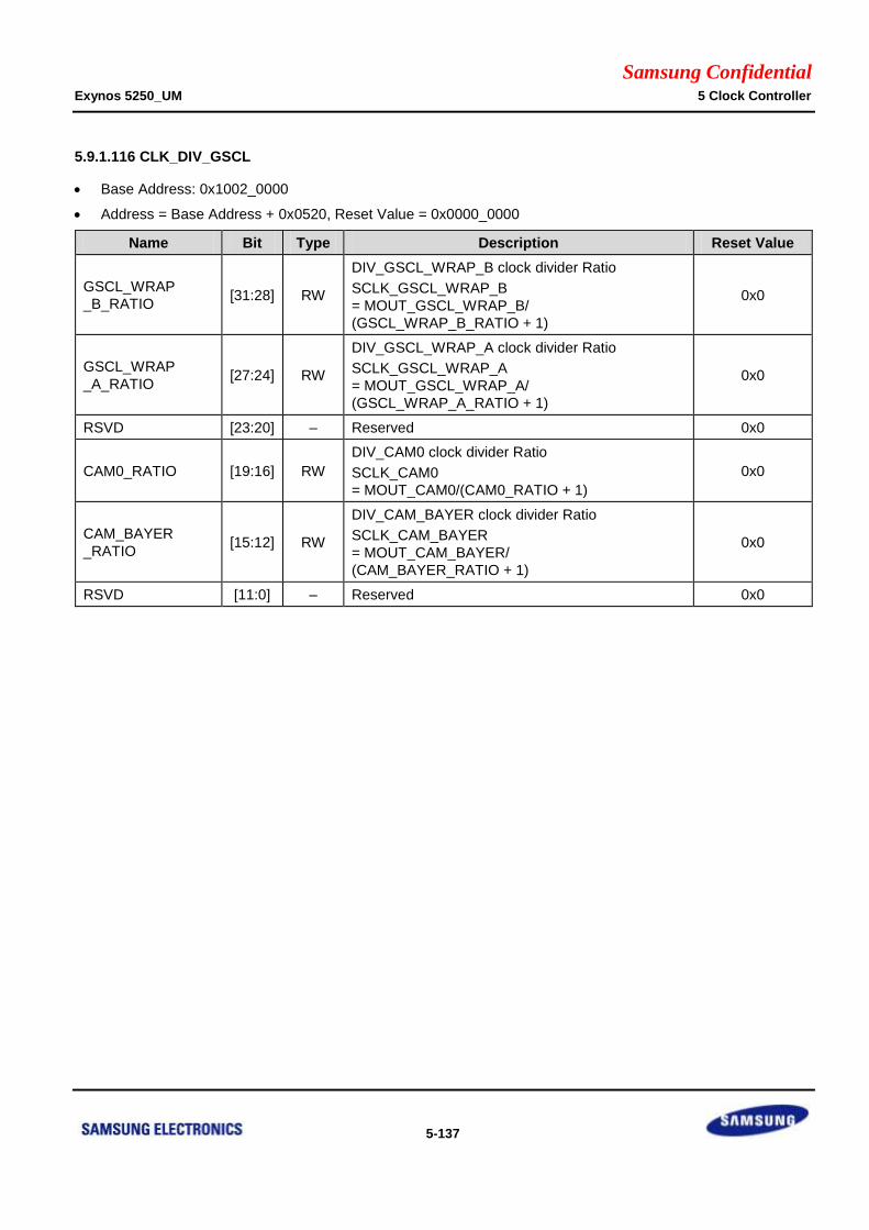
Samsung Confidential Exynos 5250_UM 5 Clock Controller
5-137
5.9.1.116 CLK_DIV_GSCL
Base Address: 0x1002_0000
Address = Base Address + 0x0520, Reset Value = 0x0000_0000
Name Bit Type Description Reset Value
GSCL_WRAP
_B_RATIO [31:28] RW
DIV_GSCL_WRAP_B clock divider Ratio
SCLK_GSCL_WRAP_B
= MOUT_GSCL_WRAP_B/
(GSCL_WRAP_B_RATIO + 1)
0x0
GSCL_WRAP
_A_RATIO [27:24] RW
DIV_GSCL_WRAP_A clock divider Ratio
SCLK_GSCL_WRAP_A
= MOUT_GSCL_WRAP_A/
(GSCL_WRAP_A_RATIO + 1)
0x0
RSVD [23:20] – Reserved 0x0
CAM0_RATIO [19:16] RW
DIV_CAM0 clock divider Ratio
SCLK_CAM0
= MOUT_CAM0/(CAM0_RATIO + 1)
0x0
CAM_BAYER
_RATIO [15:12] RW
DIV_CAM_BAYER clock divider Ratio
SCLK_CAM_BAYER
= MOUT_CAM_BAYER/
(CAM_BAYER_RATIO + 1)
0x0
RSVD [11:0] – Reserved 0x0
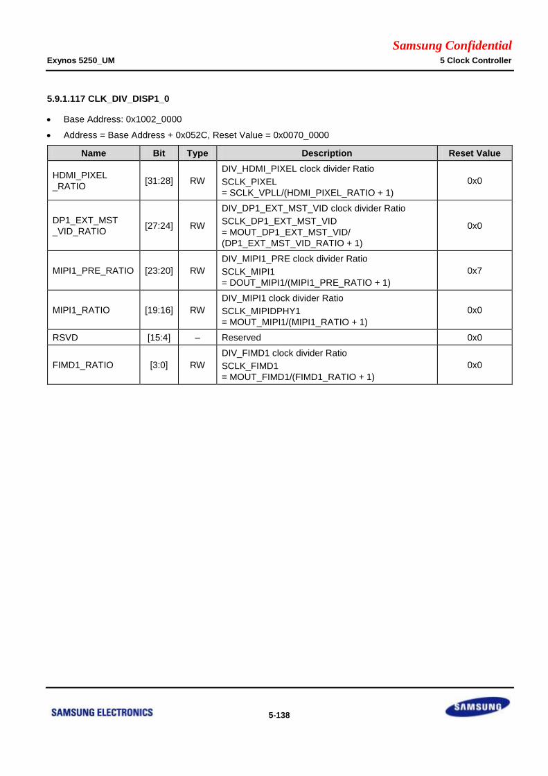
Samsung Confidential Exynos 5250_UM 5 Clock Controller
5-138
5.9.1.117 CLK_DIV_DISP1_0
Base Address: 0x1002_0000
Address = Base Address + 0x052C, Reset Value = 0x0070_0000
Name Bit Type Description Reset Value
HDMI_PIXEL
_RATIO [31:28] RW
DIV_HDMI_PIXEL clock divider Ratio
SCLK_PIXEL
= SCLK_VPLL/(HDMI_PIXEL_RATIO + 1)
0x0
DP1_EXT_MST
_VID_RATIO [27:24] RW
DIV_DP1_EXT_MST_VID clock divider Ratio
SCLK_DP1_EXT_MST_VID
= MOUT_DP1_EXT_MST_VID/
(DP1_EXT_MST_VID_RATIO + 1)
0x0
MIPI1_PRE_RATIO [23:20] RW
DIV_MIPI1_PRE clock divider Ratio
SCLK_MIPI1
= DOUT_MIPI1/(MIPI1_PRE_RATIO + 1)
0x7
MIPI1_RATIO [19:16] RW
DIV_MIPI1 clock divider Ratio
SCLK_MIPIDPHY1
= MOUT_MIPI1/(MIPI1_RATIO + 1)
0x0
RSVD [15:4] – Reserved 0x0
FIMD1_RATIO [3:0] RW
DIV_FIMD1 clock divider Ratio
SCLK_FIMD1
= MOUT_FIMD1/(FIMD1_RATIO + 1)
0x0
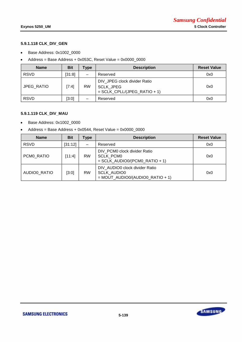
Samsung Confidential Exynos 5250_UM 5 Clock Controller
5-139
5.9.1.118 CLK_DIV_GEN
Base Address: 0x1002_0000
Address = Base Address + 0x053C, Reset Value = 0x0000_0000
Name Bit Type Description Reset Value
RSVD [31:8] – Reserved 0x0
JPEG_RATIO [7:4] RW
DIV_JPEG clock divider Ratio
SCLK_JPEG
= SCLK_CPLL/(JPEG_RATIO + 1)
0x0
RSVD [3:0] – Reserved 0x0
5.9.1.119 CLK_DIV_MAU
Base Address: 0x1002_0000
Address = Base Address + 0x0544, Reset Value = 0x0000_0000
Name Bit Type Description Reset Value
RSVD [31:12] – Reserved 0x0
PCM0_RATIO [11:4] RW
DIV_PCM0 clock divider Ratio
SCLK_PCM0
= SCLK_AUDIO0/(PCM0_RATIO + 1)
0x0
AUDIO0_RATIO [3:0] RW
DIV_AUDIO0 clock divider Ratio
SCLK_AUDIO0
= MOUT_AUDIO0/(AUDIO0_RATIO + 1)
0x0
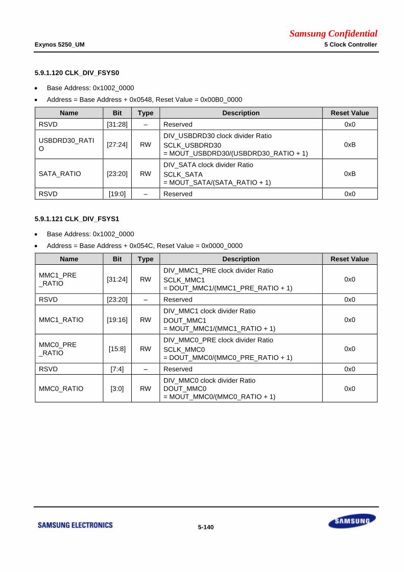
Samsung Confidential Exynos 5250_UM 5 Clock Controller
5-140
5.9.1.120 CLK_DIV_FSYS0
Base Address: 0x1002_0000
Address = Base Address + 0x0548, Reset Value = 0x00B0_0000
Name Bit Type Description Reset Value
RSVD [31:28] – Reserved 0x0
USBDRD30_RATI
O [27:24] RW
DIV_USBDRD30 clock divider Ratio
SCLK_USBDRD30
= MOUT_USBDRD30/(USBDRD30_RATIO + 1)
0xB
SATA_RATIO [23:20] RW
DIV_SATA clock divider Ratio
SCLK_SATA
= MOUT_SATA/(SATA_RATIO + 1)
0xB
RSVD [19:0] – Reserved 0x0
5.9.1.121 CLK_DIV_FSYS1
Base Address: 0x1002_0000
Address = Base Address + 0x054C, Reset Value = 0x0000_0000
Name Bit Type Description Reset Value
MMC1_PRE
_RATIO [31:24] RW
DIV_MMC1_PRE clock divider Ratio
SCLK_MMC1
= DOUT_MMC1/(MMC1_PRE_RATIO + 1)
0x0
RSVD [23:20] – Reserved 0x0
MMC1_RATIO [19:16] RW
DIV_MMC1 clock divider Ratio
DOUT_MMC1
= MOUT_MMC1/(MMC1_RATIO + 1)
0x0
MMC0_PRE
_RATIO [15:8] RW
DIV_MMC0_PRE clock divider Ratio
SCLK_MMC0
= DOUT_MMC0/(MMC0_PRE_RATIO + 1)
0x0
RSVD [7:4] – Reserved 0x0
MMC0_RATIO [3:0] RW
DIV_MMC0 clock divider Ratio
DOUT_MMC0
= MOUT_MMC0/(MMC0_RATIO + 1)
0x0

Samsung Confidential Exynos 5250_UM 5 Clock Controller
5-141
5.9.1.122 CLK_DIV_FSYS2
Base Address: 0x1002_0000
Address = Base Address + 0x0550, Reset Value = 0x0000_0000
Name Bit Type Description Reset Value
MMC3_PRE
_RATIO [31:24] RW
DIV_MMC3_PRE clock divider Ratio
SCLK_MMC3
= DOUT_MMC3/(MMC3_PRE_RATIO + 1)
0x0
RSVD [23:20] – Reserved 0x0
MMC3_RATIO [19:16] RW
DIV_MMC3 clock divider Ratio
DOUT_MMC3
= MOUT_MMC3/(MMC3_RATIO + 1)
0x0
MMC2_PRE
_RATIO [15:8] RW
DIV_MMC2_PRE clock divider Ratio
SCLK_MMC2
= DOUT_MMC2/MMC2_PRE_RATIO + 1)
0x0
RSVD [7:4] – Reserved 0x0
MMC2_RATIO [3:0] RW
DIV_MMC2 clock divider Ratio
DOUT_MMC2
= MOUT_MMC2/(MMC2_RATIO + 1)
0x0
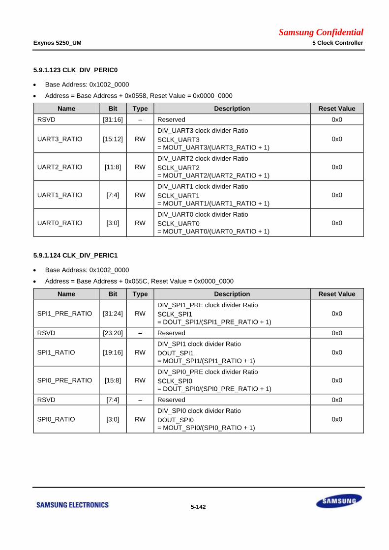
Samsung Confidential Exynos 5250_UM 5 Clock Controller
5-142
5.9.1.123 CLK_DIV_PERIC0
Base Address: 0x1002_0000
Address = Base Address + 0x0558, Reset Value = 0x0000_0000
Name Bit Type Description Reset Value
RSVD [31:16] – Reserved 0x0
UART3_RATIO [15:12] RW
DIV_UART3 clock divider Ratio
SCLK_UART3
= MOUT_UART3/(UART3_RATIO + 1)
0x0
UART2_RATIO [11:8] RW
DIV_UART2 clock divider Ratio
SCLK_UART2
= MOUT_UART2/(UART2_RATIO + 1)
0x0
UART1_RATIO [7:4] RW
DIV_UART1 clock divider Ratio
SCLK_UART1
= MOUT_UART1/(UART1_RATIO + 1)
0x0
UART0_RATIO [3:0] RW
DIV_UART0 clock divider Ratio
SCLK_UART0
= MOUT_UART0/(UART0_RATIO + 1)
0x0
5.9.1.124 CLK_DIV_PERIC1
Base Address: 0x1002_0000
Address = Base Address + 0x055C, Reset Value = 0x0000_0000
Name Bit Type Description Reset Value
SPI1_PRE_RATIO [31:24] RW
DIV_SPI1_PRE clock divider Ratio
SCLK_SPI1
= DOUT_SPI1/(SPI1_PRE_RATIO + 1)
0x0
RSVD [23:20] – Reserved 0x0
SPI1_RATIO [19:16] RW
DIV_SPI1 clock divider Ratio
DOUT_SPI1
= MOUT_SPI1/(SPI1_RATIO + 1)
0x0
SPI0_PRE_RATIO [15:8] RW
DIV_SPI0_PRE clock divider Ratio
SCLK_SPI0
= DOUT_SPI0/(SPI0_PRE_RATIO + 1)
0x0
RSVD [7:4] – Reserved 0x0
SPI0_RATIO [3:0] RW
DIV_SPI0 clock divider Ratio
DOUT_SPI0
= MOUT_SPI0/(SPI0_RATIO + 1)
0x0
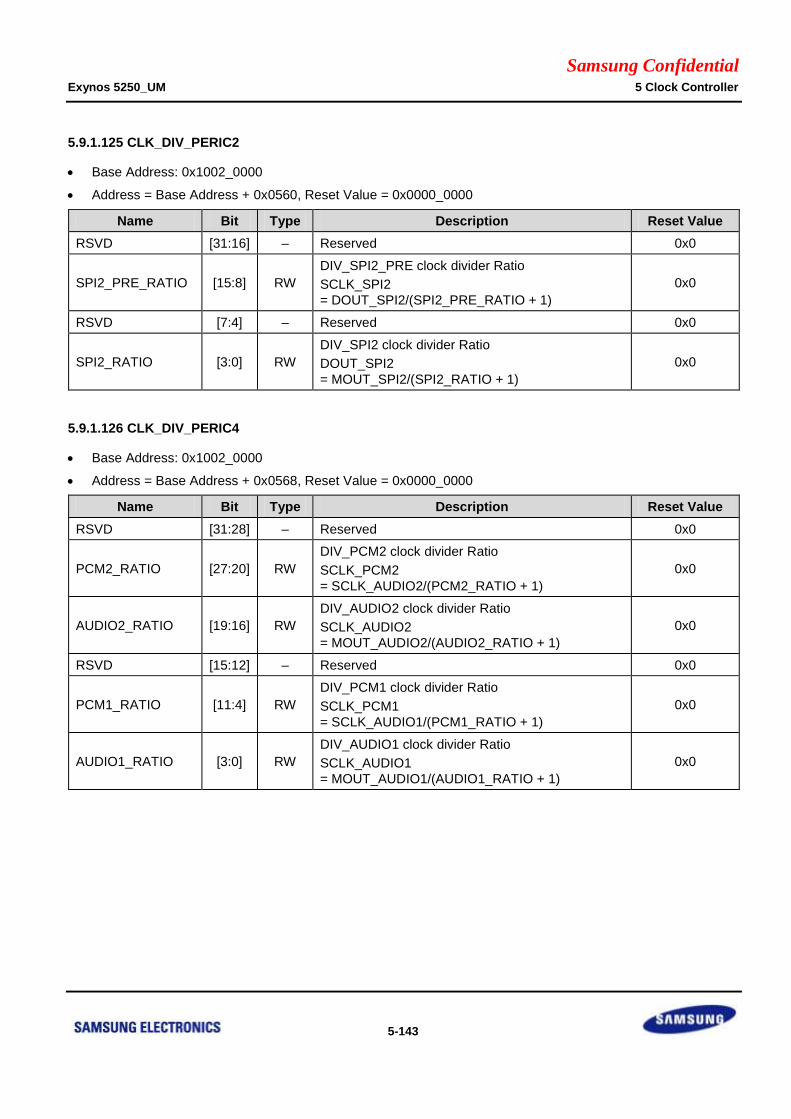
Samsung Confidential Exynos 5250_UM 5 Clock Controller
5-143
5.9.1.125 CLK_DIV_PERIC2
Base Address: 0x1002_0000
Address = Base Address + 0x0560, Reset Value = 0x0000_0000
Name Bit Type Description Reset Value
RSVD [31:16] – Reserved 0x0
SPI2_PRE_RATIO [15:8] RW
DIV_SPI2_PRE clock divider Ratio
SCLK_SPI2
= DOUT_SPI2/(SPI2_PRE_RATIO + 1)
0x0
RSVD [7:4] – Reserved 0x0
SPI2_RATIO [3:0] RW
DIV_SPI2 clock divider Ratio
DOUT_SPI2
= MOUT_SPI2/(SPI2_RATIO + 1)
0x0
5.9.1.126 CLK_DIV_PERIC4
Base Address: 0x1002_0000
Address = Base Address + 0x0568, Reset Value = 0x0000_0000
Name Bit Type Description Reset Value
RSVD [31:28] – Reserved 0x0
PCM2_RATIO [27:20] RW
DIV_PCM2 clock divider Ratio
SCLK_PCM2
= SCLK_AUDIO2/(PCM2_RATIO + 1)
0x0
AUDIO2_RATIO [19:16] RW
DIV_AUDIO2 clock divider Ratio
SCLK_AUDIO2
= MOUT_AUDIO2/(AUDIO2_RATIO + 1)
0x0
RSVD [15:12] – Reserved 0x0
PCM1_RATIO [11:4] RW
DIV_PCM1 clock divider Ratio
SCLK_PCM1
= SCLK_AUDIO1/(PCM1_RATIO + 1)
0x0
AUDIO1_RATIO [3:0] RW
DIV_AUDIO1 clock divider Ratio
SCLK_AUDIO1
= MOUT_AUDIO1/(AUDIO1_RATIO + 1)
0x0
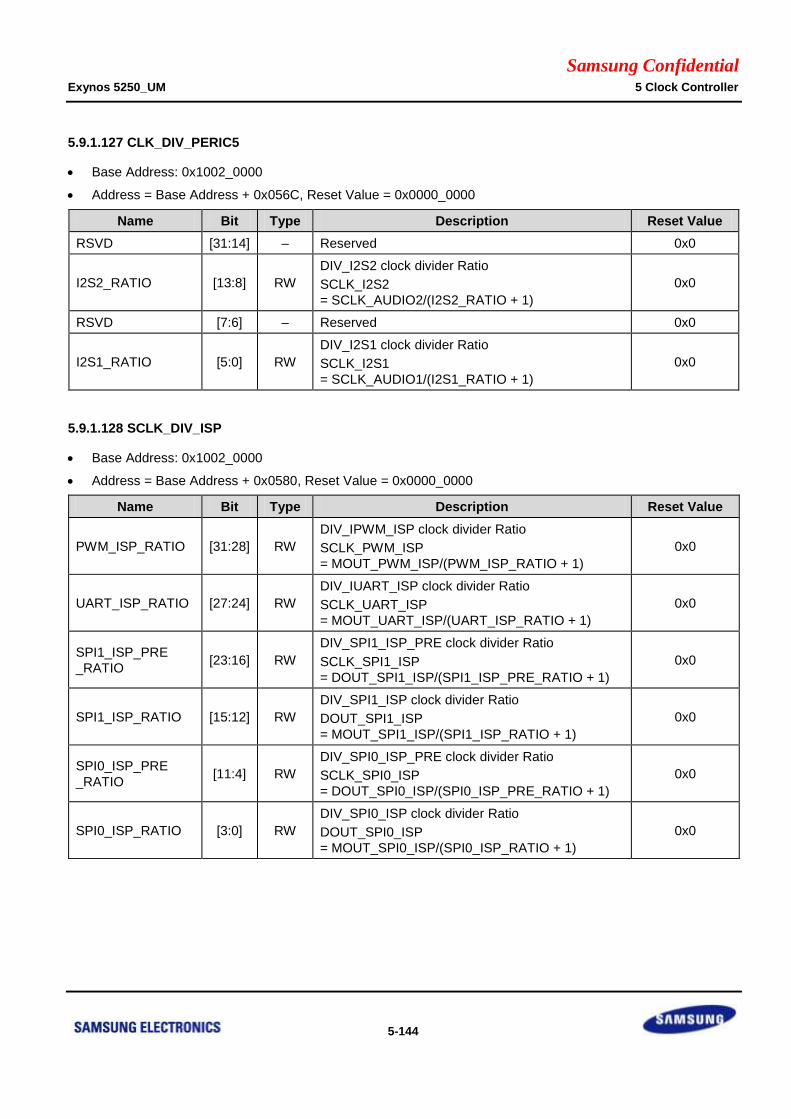
Samsung Confidential Exynos 5250_UM 5 Clock Controller
5-144
5.9.1.127 CLK_DIV_PERIC5
Base Address: 0x1002_0000
Address = Base Address + 0x056C, Reset Value = 0x0000_0000
Name Bit Type Description Reset Value
RSVD [31:14] – Reserved 0x0
I2S2_RATIO [13:8] RW
DIV_I2S2 clock divider Ratio
SCLK_I2S2
= SCLK_AUDIO2/(I2S2_RATIO + 1)
0x0
RSVD [7:6] – Reserved 0x0
I2S1_RATIO [5:0] RW
DIV_I2S1 clock divider Ratio
SCLK_I2S1
= SCLK_AUDIO1/(I2S1_RATIO + 1)
0x0
5.9.1.128 SCLK_DIV_ISP
Base Address: 0x1002_0000
Address = Base Address + 0x0580, Reset Value = 0x0000_0000
Name Bit Type Description Reset Value
PWM_ISP_RATIO [31:28] RW
DIV_IPWM_ISP clock divider Ratio
SCLK_PWM_ISP
= MOUT_PWM_ISP/(PWM_ISP_RATIO + 1)
0x0
UART_ISP_RATIO [27:24] RW
DIV_IUART_ISP clock divider Ratio
SCLK_UART_ISP
= MOUT_UART_ISP/(UART_ISP_RATIO + 1)
0x0
SPI1_ISP_PRE
_RATIO [23:16] RW
DIV_SPI1_ISP_PRE clock divider Ratio
SCLK_SPI1_ISP
= DOUT_SPI1_ISP/(SPI1_ISP_PRE_RATIO + 1)
0x0
SPI1_ISP_RATIO [15:12] RW
DIV_SPI1_ISP clock divider Ratio
DOUT_SPI1_ISP
= MOUT_SPI1_ISP/(SPI1_ISP_RATIO + 1)
0x0
SPI0_ISP_PRE
_RATIO [11:4] RW
DIV_SPI0_ISP_PRE clock divider Ratio
SCLK_SPI0_ISP
= DOUT_SPI0_ISP/(SPI0_ISP_PRE_RATIO + 1)
0x0
SPI0_ISP_RATIO [3:0] RW
DIV_SPI0_ISP clock divider Ratio
DOUT_SPI0_ISP
= MOUT_SPI0_ISP/(SPI0_ISP_RATIO + 1)
0x0
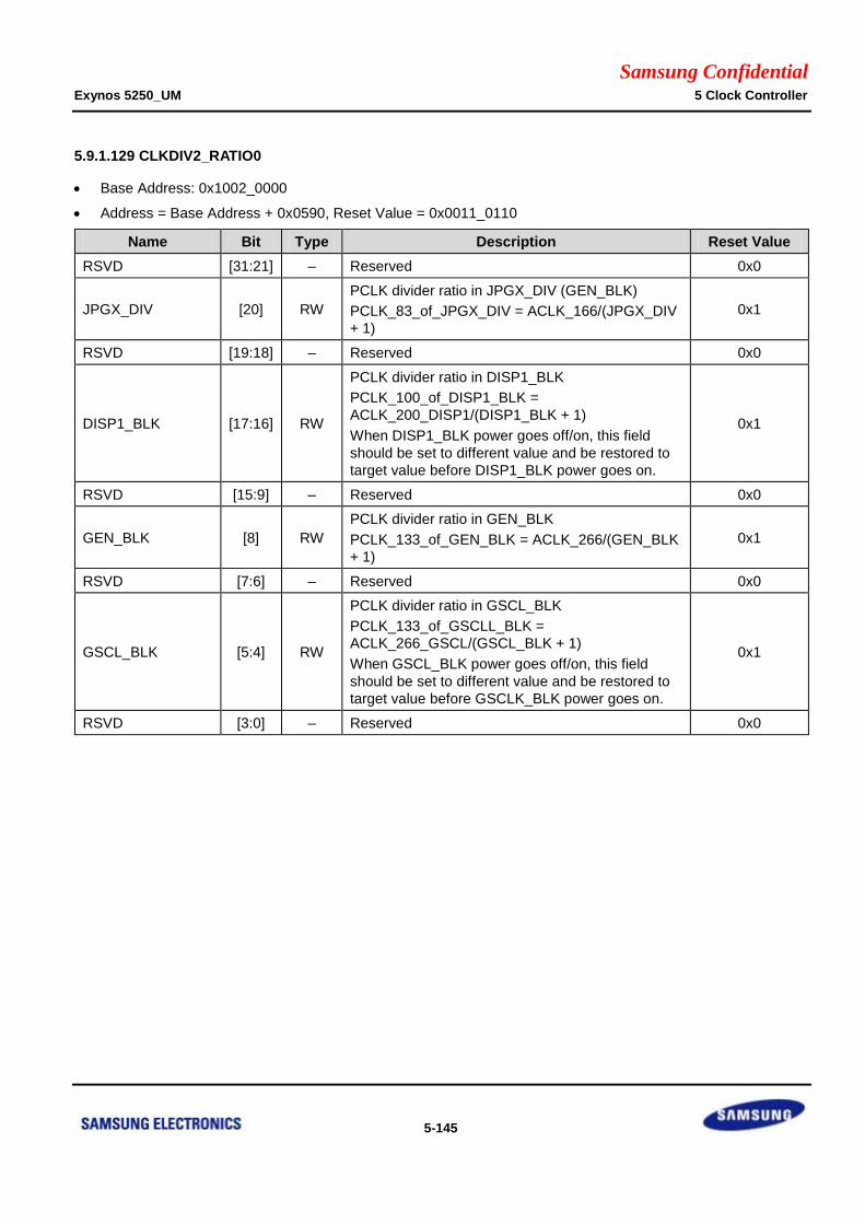
Samsung Confidential Exynos 5250_UM 5 Clock Controller
5-145
5.9.1.129 CLKDIV2_RATIO0
Base Address: 0x1002_0000
Address = Base Address + 0x0590, Reset Value = 0x0011_0110
Name Bit Type Description Reset Value
RSVD [31:21] – Reserved 0x0
JPGX_DIV [20] RW
PCLK divider ratio in JPGX_DIV (GEN_BLK)
PCLK_83_of_JPGX_DIV = ACLK_166/(JPGX_DIV
+ 1)
0x1
RSVD [19:18] – Reserved 0x0
DISP1_BLK [17:16] RW
PCLK divider ratio in DISP1_BLK
PCLK_100_of_DISP1_BLK =
ACLK_200_DISP1/(DISP1_BLK + 1)
When DISP1_BLK power goes off/on, this field
should be set to different value and be restored to
target value before DISP1_BLK power goes on.
0x1
RSVD [15:9] – Reserved 0x0
GEN_BLK [8] RW
PCLK divider ratio in GEN_BLK
PCLK_133_of_GEN_BLK = ACLK_266/(GEN_BLK
+ 1)
0x1
RSVD [7:6] – Reserved 0x0
GSCL_BLK [5:4] RW
PCLK divider ratio in GSCL_BLK
PCLK_133_of_GSCLL_BLK =
ACLK_266_GSCL/(GSCL_BLK + 1)
When GSCL_BLK power goes off/on, this field
should be set to different value and be restored to
target value before GSCLK_BLK power goes on.
0x1
RSVD [3:0] – Reserved 0x0

Samsung Confidential Exynos 5250_UM 5 Clock Controller
5-146
5.9.1.130 CLKDIV2_RATIO1
Base Address: 0x1002_0000
Address = Base Address + 0x0594, Reset Value = 0x0000_0105
Name Bit Type Description Reset Value
RSVD [31:10] – Reserved 0x0
G3D_BLK_PCLK [9:8] RW
PCLK divider ratio in G3D_BLK
PCLK_of_G3D_BLK =
ACLK_400_G3D/(G3D_BLK_PCLK + 1)
0x1
RSVD [7:4] – Reserved 0x0
FSYS_PCLKDBG [3:2] RW
PCLKDBG divider ratio in FSYS_BLK
PCLKDBG_of_FSYS_BLK =
ATCLK_of_FSYS_BLK/(FSYS_PCLKDBG + 1)
0x1
FSYS_ATCLK [1:0] RW
ATCLK divider ratio in FSYS_BLK
ATCLK_of_FSYS_BLK =
ACLK_400_IOP/(FSYS_ATCLK + 1)
0x1
5.9.1.131 CLKDIV4_RATIO
Base Address: 0x1002_0000
Address = Base Address + 0x05A0, Reset Value = 0x0000_0003
Name Bit Type Description Reset Value
RSVD [31:2] – Reserved 0x0
MFC_BLK [1:0] RW
PCLK divider ratio in MFC_BLK
PCLK_83_of_MFC_BLK = ACLK_333/(MFC_BLK
+ 1)
When MFC power goes off/on, this field should be
set to different value and be restored to target
value before MFC power goes on.
0x3
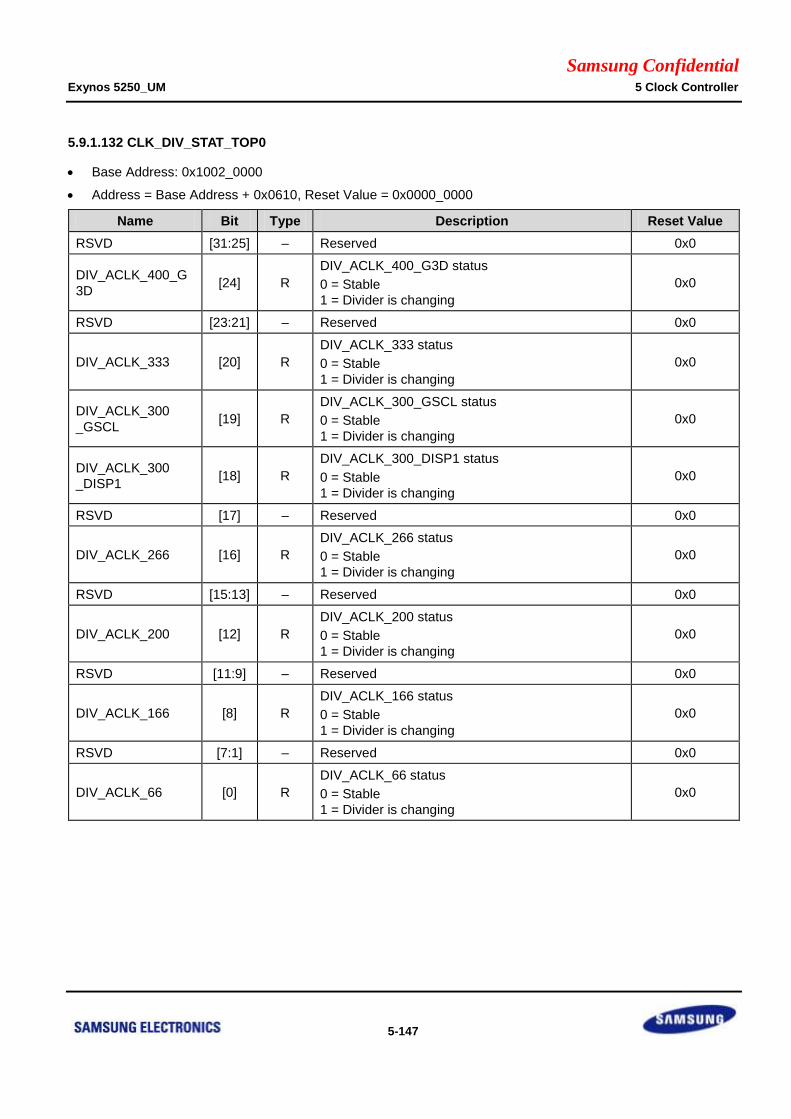
Samsung Confidential Exynos 5250_UM 5 Clock Controller
5-147
5.9.1.132 CLK_DIV_STAT_TOP0
Base Address: 0x1002_0000
Address = Base Address + 0x0610, Reset Value = 0x0000_0000
Name Bit Type Description Reset Value
RSVD [31:25] – Reserved 0x0
DIV_ACLK_400_G
3D [24] R
DIV_ACLK_400_G3D status
0 = Stable
1 = Divider is changing
0x0
RSVD [23:21] – Reserved 0x0
DIV_ACLK_333 [20] R
DIV_ACLK_333 status
0 = Stable
1 = Divider is changing
0x0
DIV_ACLK_300
_GSCL [19] R
DIV_ACLK_300_GSCL status
0 = Stable
1 = Divider is changing
0x0
DIV_ACLK_300
_DISP1 [18] R
DIV_ACLK_300_DISP1 status
0 = Stable
1 = Divider is changing
0x0
RSVD [17] – Reserved 0x0
DIV_ACLK_266 [16] R
DIV_ACLK_266 status
0 = Stable
1 = Divider is changing
0x0
RSVD [15:13] – Reserved 0x0
DIV_ACLK_200 [12] R
DIV_ACLK_200 status
0 = Stable
1 = Divider is changing
0x0
RSVD [11:9] – Reserved 0x0
DIV_ACLK_166 [8] R
DIV_ACLK_166 status
0 = Stable
1 = Divider is changing
0x0
RSVD [7:1] – Reserved 0x0
DIV_ACLK_66 [0] R
DIV_ACLK_66 status
0 = Stable
1 = Divider is changing
0x0
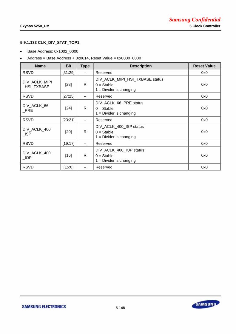
Samsung Confidential Exynos 5250_UM 5 Clock Controller
5-148
5.9.1.133 CLK_DIV_STAT_TOP1
Base Address: 0x1002_0000
Address = Base Address + 0x0614, Reset Value = 0x0000_0000
Name Bit Type Description Reset Value
RSVD [31:29] – Reserved 0x0
DIV_ACLK_MIPI
_HSI_TXBASE [28] R
DIV_ACLK_MIPI_HSI_TXBASE status
0 = Stable
1 = Divider is changing
0x0
RSVD [27:25] – Reserved 0x0
DIV_ACLK_66
_PRE [24] R
DIV_ACLK_66_PRE status
0 = Stable
1 = Divider is changing
0x0
RSVD [23:21] – Reserved 0x0
DIV_ACLK_400
_ISP [20] R
DIV_ACLK_400_ISP status
0 = Stable
1 = Divider is changing
0x0
RSVD [19:17] – Reserved 0x0
DIV_ACLK_400
_IOP [16] R
DIV_ACLK_400_IOP status
0 = Stable
1 = Divider is changing
0x0
RSVD [15:0] – Reserved 0x0
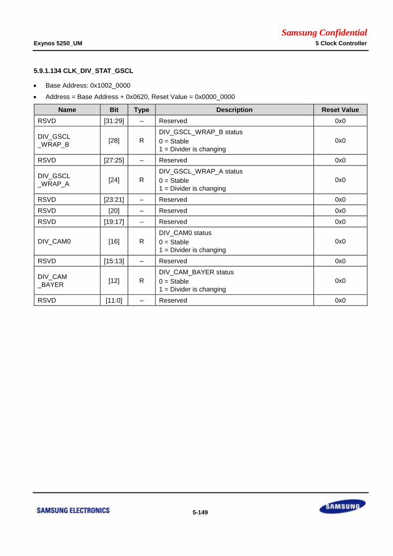
Samsung Confidential Exynos 5250_UM 5 Clock Controller
5-149
5.9.1.134 CLK_DIV_STAT_GSCL
Base Address: 0x1002_0000
Address = Base Address + 0x0620, Reset Value = 0x0000_0000
Name Bit Type Description Reset Value
RSVD [31:29] – Reserved 0x0
DIV_GSCL
_WRAP_B [28] R
DIV_GSCL_WRAP_B status
0 = Stable
1 = Divider is changing
0x0
RSVD [27:25] – Reserved 0x0
DIV_GSCL
_WRAP_A [24] R
DIV_GSCL_WRAP_A status
0 = Stable
1 = Divider is changing
0x0
RSVD [23:21] – Reserved 0x0
RSVD [20] – Reserved 0x0
RSVD [19:17] – Reserved 0x0
DIV_CAM0 [16] R
DIV_CAM0 status
0 = Stable
1 = Divider is changing
0x0
RSVD [15:13] – Reserved 0x0
DIV_CAM
_BAYER [12] R
DIV_CAM_BAYER status
0 = Stable
1 = Divider is changing
0x0
RSVD [11:0] – Reserved 0x0
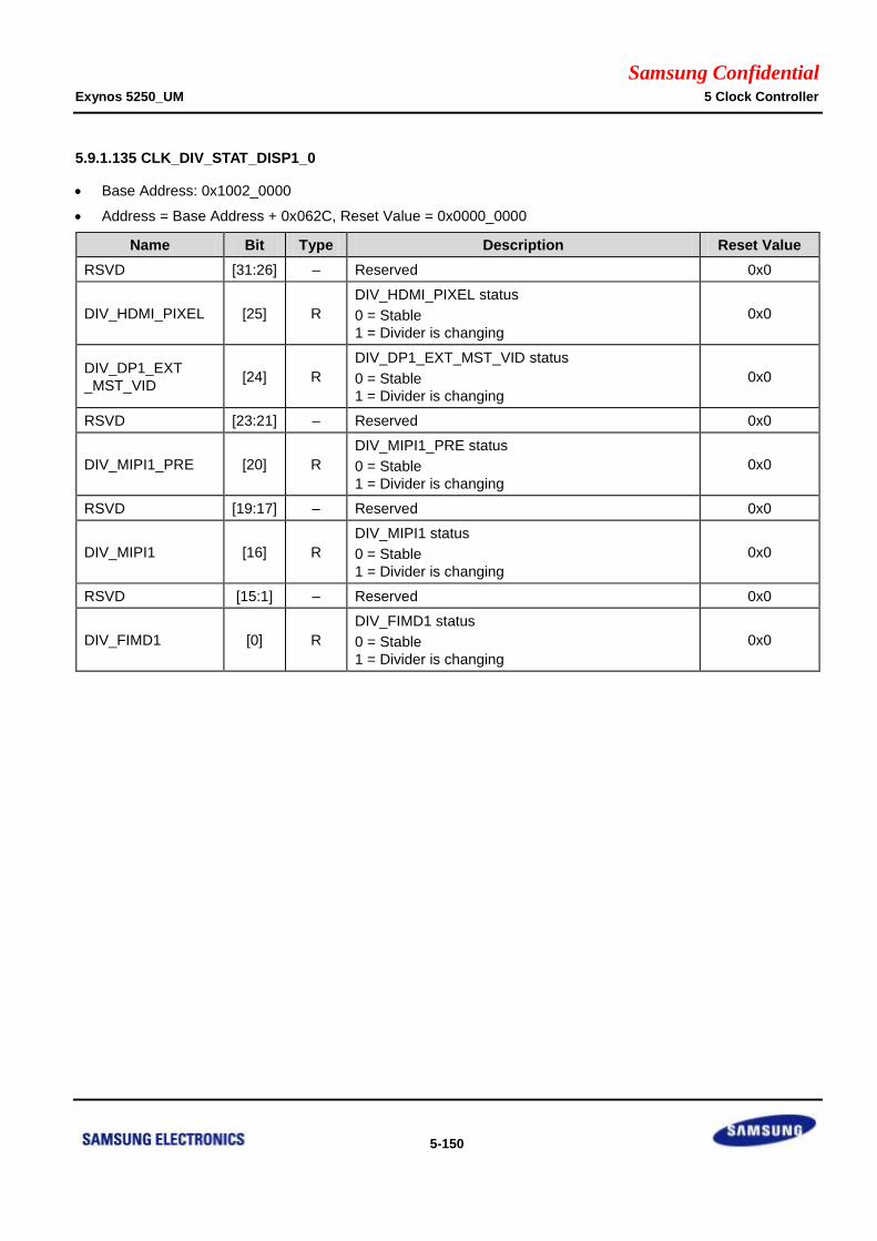
Samsung Confidential Exynos 5250_UM 5 Clock Controller
5-150
5.9.1.135 CLK_DIV_STAT_DISP1_0
Base Address: 0x1002_0000
Address = Base Address + 0x062C, Reset Value = 0x0000_0000
Name Bit Type Description Reset Value
RSVD [31:26] – Reserved 0x0
DIV_HDMI_PIXEL [25] R
DIV_HDMI_PIXEL status
0 = Stable
1 = Divider is changing
0x0
DIV_DP1_EXT
_MST_VID [24] R
DIV_DP1_EXT_MST_VID status
0 = Stable
1 = Divider is changing
0x0
RSVD [23:21] – Reserved 0x0
DIV_MIPI1_PRE [20] R
DIV_MIPI1_PRE status
0 = Stable
1 = Divider is changing
0x0
RSVD [19:17] – Reserved 0x0
DIV_MIPI1 [16] R
DIV_MIPI1 status
0 = Stable
1 = Divider is changing
0x0
RSVD [15:1] – Reserved 0x0
DIV_FIMD1 [0] R
DIV_FIMD1 status
0 = Stable
1 = Divider is changing
0x0
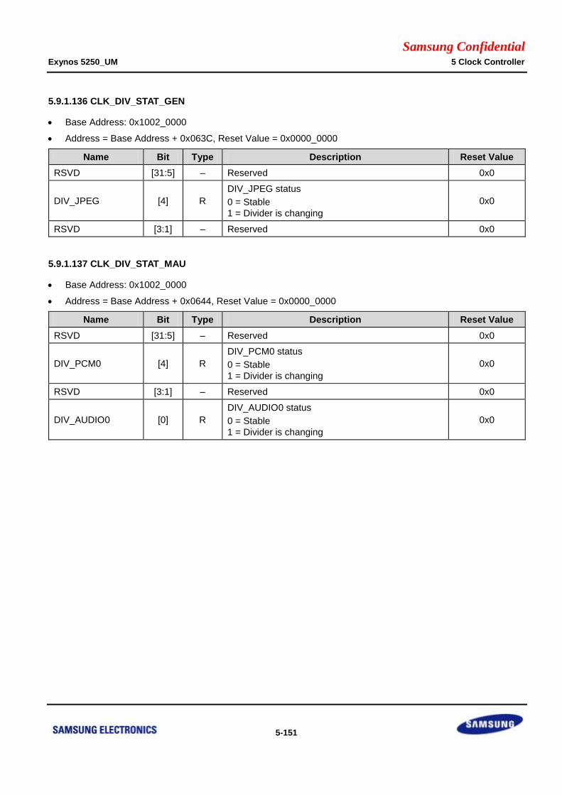
Samsung Confidential Exynos 5250_UM 5 Clock Controller
5-151
5.9.1.136 CLK_DIV_STAT_GEN
Base Address: 0x1002_0000
Address = Base Address + 0x063C, Reset Value = 0x0000_0000
Name Bit Type Description Reset Value
RSVD [31:5] – Reserved 0x0
DIV_JPEG [4] R
DIV_JPEG status
0 = Stable
1 = Divider is changing
0x0
RSVD [3:1] – Reserved 0x0
5.9.1.137 CLK_DIV_STAT_MAU
Base Address: 0x1002_0000
Address = Base Address + 0x0644, Reset Value = 0x0000_0000
Name Bit Type Description Reset Value
RSVD [31:5] – Reserved 0x0
DIV_PCM0 [4] R
DIV_PCM0 status
0 = Stable
1 = Divider is changing
0x0
RSVD [3:1] – Reserved 0x0
DIV_AUDIO0 [0] R
DIV_AUDIO0 status
0 = Stable
1 = Divider is changing
0x0
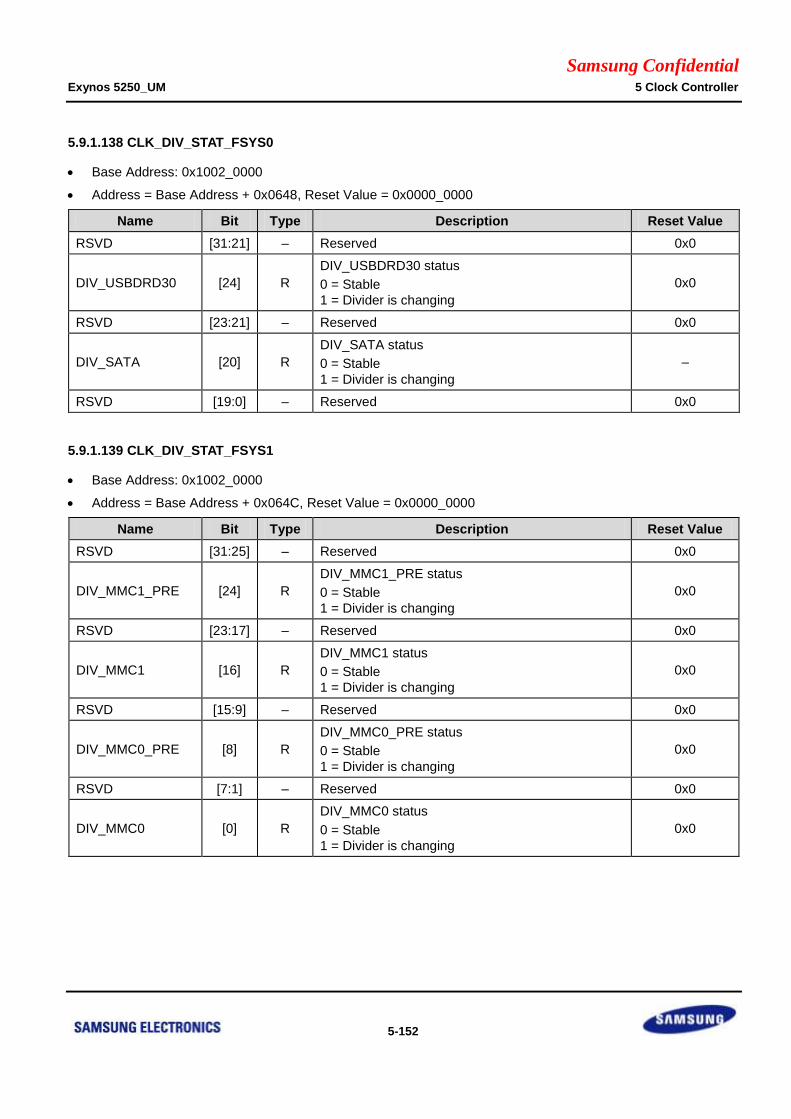
Samsung Confidential Exynos 5250_UM 5 Clock Controller
5-152
5.9.1.138 CLK_DIV_STAT_FSYS0
Base Address: 0x1002_0000
Address = Base Address + 0x0648, Reset Value = 0x0000_0000
Name Bit Type Description Reset Value
RSVD [31:21] – Reserved 0x0
DIV_USBDRD30 [24] R
DIV_USBDRD30 status
0 = Stable
1 = Divider is changing
0x0
RSVD [23:21] – Reserved 0x0
DIV_SATA [20] R
DIV_SATA status
0 = Stable
1 = Divider is changing
–
RSVD [19:0] – Reserved 0x0
5.9.1.139 CLK_DIV_STAT_FSYS1
Base Address: 0x1002_0000
Address = Base Address + 0x064C, Reset Value = 0x0000_0000
Name Bit Type Description Reset Value
RSVD [31:25] – Reserved 0x0
DIV_MMC1_PRE [24] R
DIV_MMC1_PRE status
0 = Stable
1 = Divider is changing
0x0
RSVD [23:17] – Reserved 0x0
DIV_MMC1 [16] R
DIV_MMC1 status
0 = Stable
1 = Divider is changing
0x0
RSVD [15:9] – Reserved 0x0
DIV_MMC0_PRE [8] R
DIV_MMC0_PRE status
0 = Stable
1 = Divider is changing
0x0
RSVD [7:1] – Reserved 0x0
DIV_MMC0 [0] R
DIV_MMC0 status
0 = Stable
1 = Divider is changing
0x0

Samsung Confidential Exynos 5250_UM 5 Clock Controller
5-153
5.9.1.140 CLK_DIV_STAT_FSYS2
Base Address: 0x1002_0000
Address = Base Address + 0x0650, Reset Value = 0x0000_0000
Name Bit Type Description Reset Value
RSVD [31:25] – Reserved 0x0
DIV_MMC3_PRE [24] R
DIV_MMC3_PRE status
0 = Stable
1 = Divider is changing
0x0
RSVD [23:17] – Reserved 0x0
DIV_MMC3 [16] R
DIV_MMC3 status
0 = Stable
1 = Divider is changing
0x0
RSVD [15:9] – Reserved 0x0
DIV_MMC2_PRE [8] R
DIV_MMC2_PRE status
0 = Stable
1 = Divider is changing
0x0
RSVD [7:1] – Reserved 0x0
DIV_MMC2 [0] R
DIV_MMC2 status
0 = Stable
1 = Divider is changing
0x0

Samsung Confidential Exynos 5250_UM 5 Clock Controller
5-154
5.9.1.141 CLK_DIV_STAT_PERIC0
Base Address: 0x1002_0000
Address = Base Address + 0x0658, Reset Value = 0x0000_0000
Name Bit Type Description Reset Value
RSVD [31:13] – Reserved 0x0
DIV_UART3 [12] R
DIV_UART3 status
0 = Stable
1 = Divider is changing
0x0
RSVD [11:9] – Reserved 0x0
DIV_UART2 [8] R
DIV_UART2 status
0 = Stable
1 = Divider is changing
0x0
RSVD [7:5] – Reserved 0x0
DIV_UART1 [4] R
DIV_UART1 status
0 = Stable
1 = Divider is changing
0x0
RSVD [3:1] – Reserved 0x0
DIV_UART0 [0] R
DIV_UART0 status
0 = Stable
1 = Divider is changing
0x0
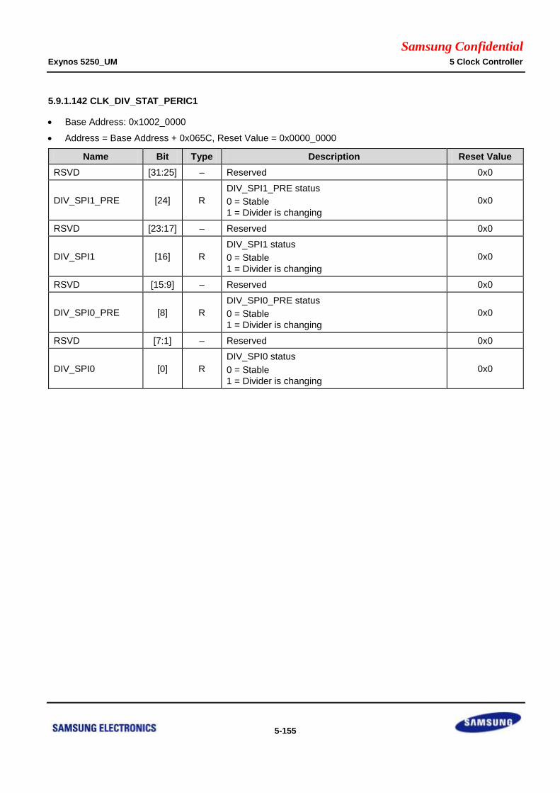
Samsung Confidential Exynos 5250_UM 5 Clock Controller
5-155
5.9.1.142 CLK_DIV_STAT_PERIC1
Base Address: 0x1002_0000
Address = Base Address + 0x065C, Reset Value = 0x0000_0000
Name Bit Type Description Reset Value
RSVD [31:25] – Reserved 0x0
DIV_SPI1_PRE [24] R
DIV_SPI1_PRE status
0 = Stable
1 = Divider is changing
0x0
RSVD [23:17] – Reserved 0x0
DIV_SPI1 [16] R
DIV_SPI1 status
0 = Stable
1 = Divider is changing
0x0
RSVD [15:9] – Reserved 0x0
DIV_SPI0_PRE [8] R
DIV_SPI0_PRE status
0 = Stable
1 = Divider is changing
0x0
RSVD [7:1] – Reserved 0x0
DIV_SPI0 [0] R
DIV_SPI0 status
0 = Stable
1 = Divider is changing
0x0
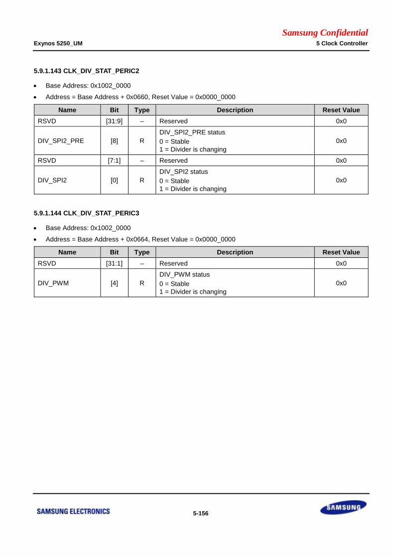
Samsung Confidential Exynos 5250_UM 5 Clock Controller
5-156
5.9.1.143 CLK_DIV_STAT_PERIC2
Base Address: 0x1002_0000
Address = Base Address + 0x0660, Reset Value = 0x0000_0000
Name Bit Type Description Reset Value
RSVD [31:9] – Reserved 0x0
DIV_SPI2_PRE [8] R
DIV_SPI2_PRE status
0 = Stable
1 = Divider is changing
0x0
RSVD [7:1] – Reserved 0x0
DIV_SPI2 [0] R
DIV_SPI2 status
0 = Stable
1 = Divider is changing
0x0
5.9.1.144 CLK_DIV_STAT_PERIC3
Base Address: 0x1002_0000
Address = Base Address + 0x0664, Reset Value = 0x0000_0000
Name Bit Type Description Reset Value
RSVD [31:1] – Reserved 0x0
DIV_PWM [4] R
DIV_PWM status
0 = Stable
1 = Divider is changing
0x0
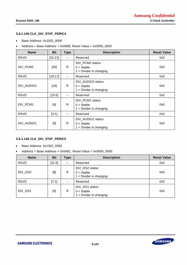
Samsung Confidential Exynos 5250_UM 5 Clock Controller
5-157
5.9.1.145 CLK_DIV_STAT_PERIC4
Base Address: 0x1002_0000
Address = Base Address + 0x0668, Reset Value = 0x0000_0000
Name Bit Type Description Reset Value
RSVD [31:21] – Reserved 0x0
DIV_PCM2 [20] R
DIV_PCM2 status
0 = Stable
1 = Divider is changing
0x0
RSVD [19:17] – Reserved 0x0
DIV_AUDIO2 [16] R
DIV_AUDIO2 status
0 = Stable
1 = Divider is changing
0x0
RSVD [15:5] – Reserved 0x0
DIV_PCM1 [4] R
DIV_PCM1 status
0 = Stable
1 = Divider is changing
0x0
RSVD [3:1] – Reserved 0x0
DIV_AUDIO1 [0] R
DIV_AUDIO1 status
0 = Stable
1 = Divider is changing
0x0
5.9.1.146 CLK_DIV_STAT_PERIC5
Base Address: 0x1002_0000
Address = Base Address + 0x066C, Reset Value = 0x0000_0000
Name Bit Type Description Reset Value
RSVD [31:9] – Reserved 0x0
DIV_I2S2 [8] R
DIV_I2S2 status
0 = Stable
1 = Divider is changing
0x0
RSVD [7:1] – Reserved 0x0
DIV_I2S1 [0] R
DIV_I2S1 status
0 = Stable
1 = Divider is changing
0x0
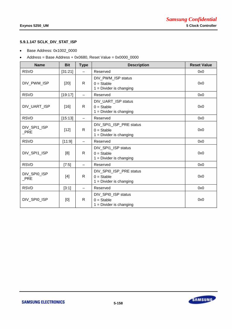
Samsung Confidential Exynos 5250_UM 5 Clock Controller
5-158
5.9.1.147 SCLK_DIV_STAT_ISP
Base Address: 0x1002_0000
Address = Base Address + 0x0680, Reset Value = 0x0000_0000
Name Bit Type Description Reset Value
RSVD [31:21] – Reserved 0x0
DIV_PWM_ISP [20] R
DIV_PWM_ISP status
0 = Stable
1 = Divider is changing
0x0
RSVD [19:17] – Reserved 0x0
DIV_UART_ISP [16] R
DIV_UART_ISP status
0 = Stable
1 = Divider is changing
0x0
RSVD [15:13] – Reserved 0x0
DIV_SPI1_ISP
_PRE [12] R
DIV_SPI1_ISP_PRE status
0 = Stable
1 = Divider is changing
0x0
RSVD [11:9] – Reserved 0x0
DIV_SPI1_ISP [8] R
DIV_SPI1_ISP status
0 = Stable
1 = Divider is changing
0x0
RSVD [7:5] – Reserved 0x0
DIV_SPI0_ISP
_PRE [4] R
DIV_SPI0_ISP_PRE status
0 = Stable
1 = Divider is changing
0x0
RSVD [3:1] – Reserved 0x0
DIV_SPI0_ISP [0] R
DIV_SPI0_ISP status
0 = Stable
1 = Divider is changing
0x0
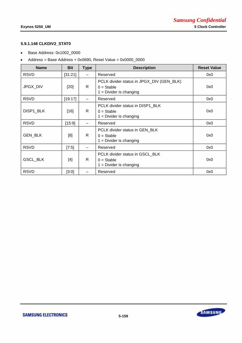
Samsung Confidential Exynos 5250_UM 5 Clock Controller
5-159
5.9.1.148 CLKDIV2_STAT0
Base Address: 0x1002_0000
Address = Base Address + 0x0690, Reset Value = 0x0000_0000
Name Bit Type Description Reset Value
RSVD [31:21] – Reserved 0x0
JPGX_DIV [20] R
PCLK divider status in JPGX_DIV (GEN_BLK)
0 = Stable
1 = Divider is changing
0x0
RSVD [19:17] – Reserved 0x0
DISP1_BLK [16] R
PCLK divider status in DISP1_BLK
0 = Stable
1 = Divider is changing
0x0
RSVD [15:9] – Reserved 0x0
GEN_BLK [8] R
PCLK divider status in GEN_BLK
0 = Stable
1 = Divider is changing
0x0
RSVD [7:5] – Reserved 0x0
GSCL_BLK [4] R
PCLK divider status in GSCL_BLK
0 = Stable
1 = Divider is changing
0x0
RSVD [3:0] – Reserved 0x0
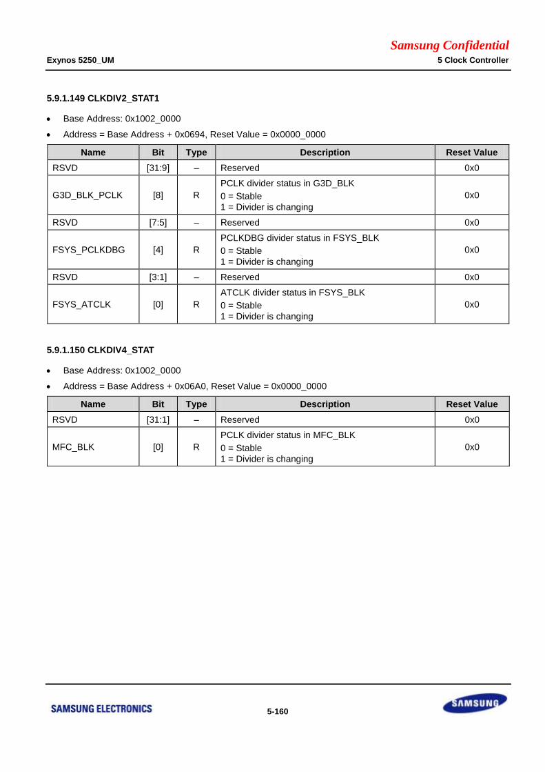
Samsung Confidential Exynos 5250_UM 5 Clock Controller
5-160
5.9.1.149 CLKDIV2_STAT1
Base Address: 0x1002_0000
Address = Base Address + 0x0694, Reset Value = 0x0000_0000
Name Bit Type Description Reset Value
RSVD [31:9] – Reserved 0x0
G3D_BLK_PCLK [8] R
PCLK divider status in G3D_BLK
0 = Stable
1 = Divider is changing
0x0
RSVD [7:5] – Reserved 0x0
FSYS_PCLKDBG [4] R
PCLKDBG divider status in FSYS_BLK
0 = Stable
1 = Divider is changing
0x0
RSVD [3:1] – Reserved 0x0
FSYS_ATCLK [0] R
ATCLK divider status in FSYS_BLK
0 = Stable
1 = Divider is changing
0x0
5.9.1.150 CLKDIV4_STAT
Base Address: 0x1002_0000
Address = Base Address + 0x06A0, Reset Value = 0x0000_0000
Name Bit Type Description Reset Value
RSVD [31:1] – Reserved 0x0
MFC_BLK [0] R
PCLK divider status in MFC_BLK
0 = Stable
1 = Divider is changing
0x0
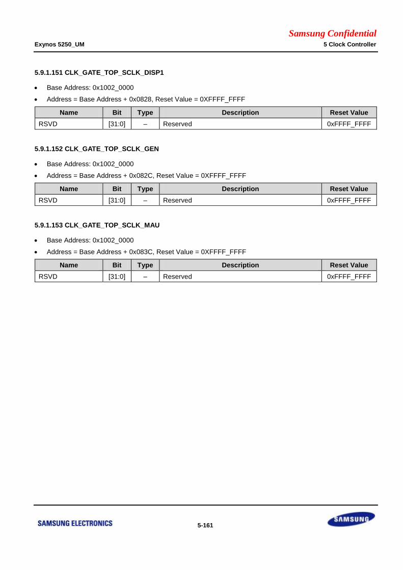
Samsung Confidential Exynos 5250_UM 5 Clock Controller
5-161
5.9.1.151 CLK_GATE_TOP_SCLK_DISP1
Base Address: 0x1002_0000
Address = Base Address + 0x0828, Reset Value = 0XFFFF_FFFF
Name Bit Type Description Reset Value
RSVD [31:0] – Reserved 0xFFFF_FFFF
5.9.1.152 CLK_GATE_TOP_SCLK_GEN
Base Address: 0x1002_0000
Address = Base Address + 0x082C, Reset Value = 0XFFFF_FFFF
Name Bit Type Description Reset Value
RSVD [31:0] – Reserved 0xFFFF_FFFF
5.9.1.153 CLK_GATE_TOP_SCLK_MAU
Base Address: 0x1002_0000
Address = Base Address + 0x083C, Reset Value = 0XFFFF_FFFF
Name Bit Type Description Reset Value
RSVD [31:0] – Reserved 0xFFFF_FFFF
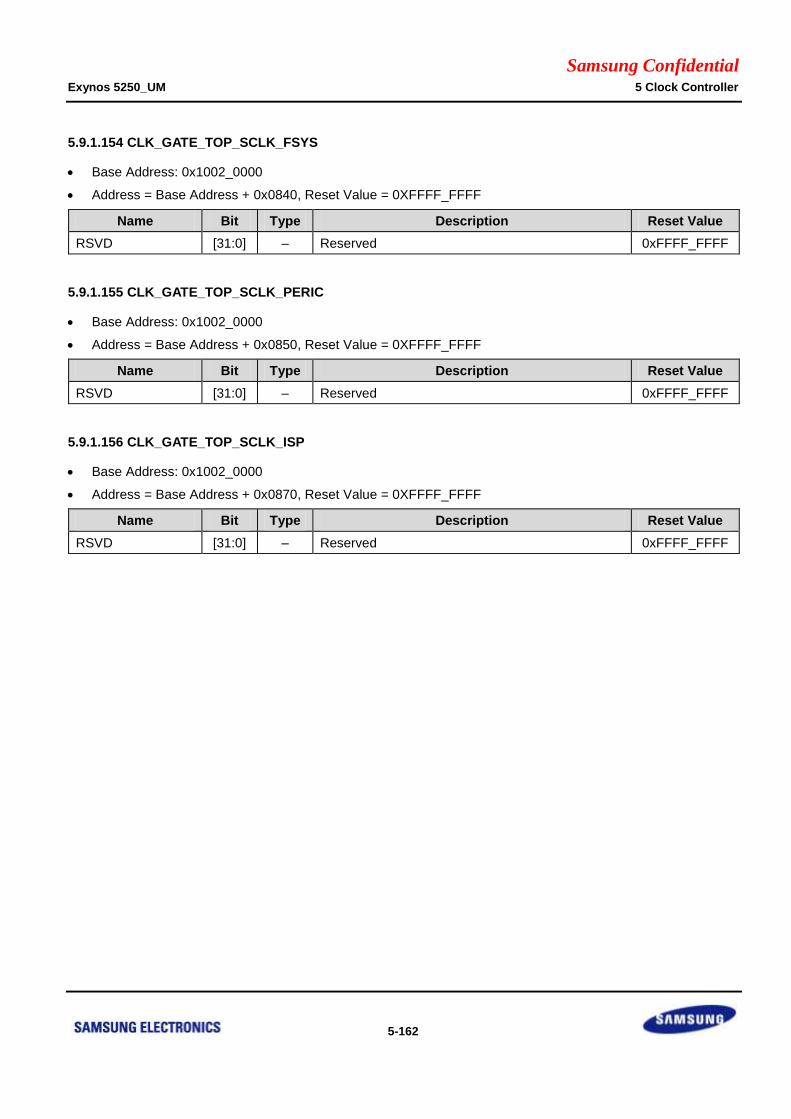
Samsung Confidential Exynos 5250_UM 5 Clock Controller
5-162
5.9.1.154 CLK_GATE_TOP_SCLK_FSYS
Base Address: 0x1002_0000
Address = Base Address + 0x0840, Reset Value = 0XFFFF_FFFF
Name Bit Type Description Reset Value
RSVD [31:0] – Reserved 0xFFFF_FFFF
5.9.1.155 CLK_GATE_TOP_SCLK_PERIC
Base Address: 0x1002_0000
Address = Base Address + 0x0850, Reset Value = 0XFFFF_FFFF
Name Bit Type Description Reset Value
RSVD [31:0] – Reserved 0xFFFF_FFFF
5.9.1.156 CLK_GATE_TOP_SCLK_ISP
Base Address: 0x1002_0000
Address = Base Address + 0x0870, Reset Value = 0XFFFF_FFFF
Name Bit Type Description Reset Value
RSVD [31:0] – Reserved 0xFFFF_FFFF
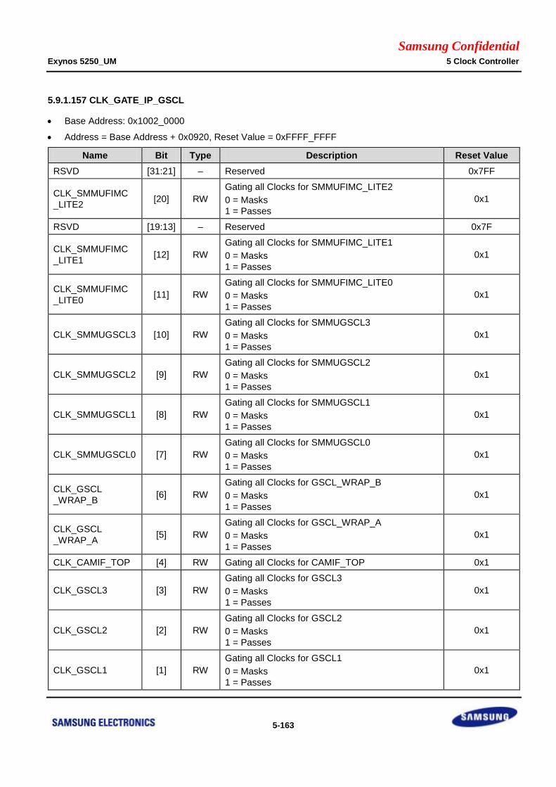
Samsung Confidential Exynos 5250_UM 5 Clock Controller
5-163
5.9.1.157 CLK_GATE_IP_GSCL
Base Address: 0x1002_0000
Address = Base Address + 0x0920, Reset Value = 0xFFFF_FFFF
Name Bit Type Description Reset Value
RSVD [31:21] – Reserved 0x7FF
CLK_SMMUFIMC
_LITE2 [20] RW
Gating all Clocks for SMMUFIMC_LITE2
0 = Masks
1 = Passes
0x1
RSVD [19:13] – Reserved 0x7F
CLK_SMMUFIMC
_LITE1 [12] RW
Gating all Clocks for SMMUFIMC_LITE1
0 = Masks
1 = Passes
0x1
CLK_SMMUFIMC
_LITE0 [11] RW
Gating all Clocks for SMMUFIMC_LITE0
0 = Masks
1 = Passes
0x1
CLK_SMMUGSCL3 [10] RW
Gating all Clocks for SMMUGSCL3
0 = Masks
1 = Passes
0x1
CLK_SMMUGSCL2 [9] RW
Gating all Clocks for SMMUGSCL2
0 = Masks
1 = Passes
0x1
CLK_SMMUGSCL1 [8] RW
Gating all Clocks for SMMUGSCL1
0 = Masks
1 = Passes
0x1
CLK_SMMUGSCL0 [7] RW
Gating all Clocks for SMMUGSCL0
0 = Masks
1 = Passes
0x1
CLK_GSCL
_WRAP_B [6] RW
Gating all Clocks for GSCL_WRAP_B
0 = Masks
1 = Passes
0x1
CLK_GSCL
_WRAP_A [5] RW
Gating all Clocks for GSCL_WRAP_A
0 = Masks
1 = Passes
0x1
CLK_CAMIF_TOP [4] RW Gating all Clocks for CAMIF_TOP 0x1
CLK_GSCL3 [3] RW
Gating all Clocks for GSCL3
0 = Masks
1 = Passes
0x1
CLK_GSCL2 [2] RW
Gating all Clocks for GSCL2
0 = Masks
1 = Passes
0x1
CLK_GSCL1 [1] RW
Gating all Clocks for GSCL1
0 = Masks
1 = Passes
0x1
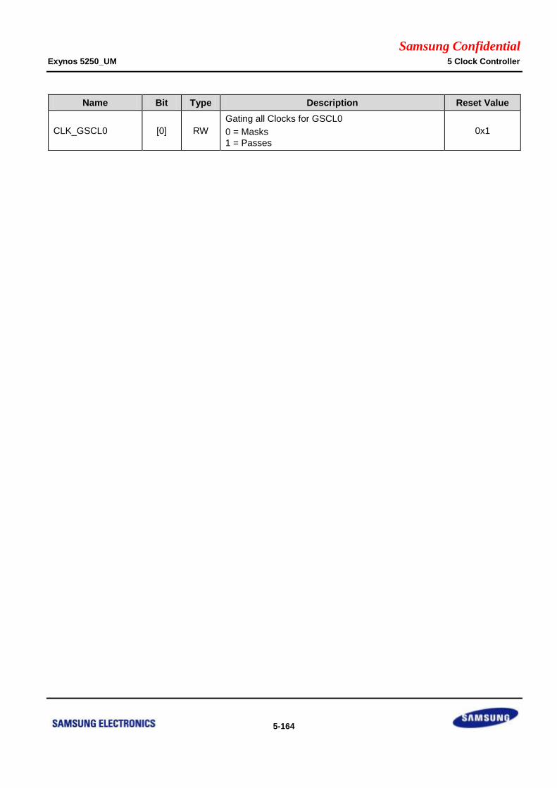
Samsung Confidential Exynos 5250_UM 5 Clock Controller
5-164
Name Bit Type Description Reset Value
CLK_GSCL0 [0] RW
Gating all Clocks for GSCL0
0 = Masks
1 = Passes
0x1
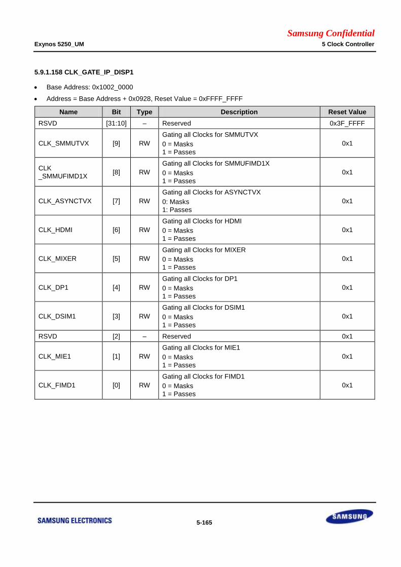
Samsung Confidential Exynos 5250_UM 5 Clock Controller
5-165
5.9.1.158 CLK_GATE_IP_DISP1
Base Address: 0x1002_0000
Address = Base Address + 0x0928, Reset Value = 0xFFFF_FFFF
Name Bit Type Description Reset Value
RSVD [31:10] – Reserved 0x3F_FFFF
CLK_SMMUTVX [9] RW
Gating all Clocks for SMMUTVX
0 = Masks
1 = Passes
0x1
CLK
_SMMUFIMD1X [8] RW
Gating all Clocks for SMMUFIMD1X
0 = Masks
1 = Passes
0x1
CLK_ASYNCTVX [7] RW
Gating all Clocks for ASYNCTVX
0: Masks
1: Passes
0x1
CLK_HDMI [6] RW
Gating all Clocks for HDMI
0 = Masks
1 = Passes
0x1
CLK_MIXER [5] RW
Gating all Clocks for MIXER
0 = Masks
1 = Passes
0x1
CLK_DP1 [4] RW
Gating all Clocks for DP1
0 = Masks
1 = Passes
0x1
CLK_DSIM1 [3] RW
Gating all Clocks for DSIM1
0 = Masks
1 = Passes
0x1
RSVD [2] – Reserved 0x1
CLK_MIE1 [1] RW
Gating all Clocks for MIE1
0 = Masks
1 = Passes
0x1
CLK_FIMD1 [0] RW
Gating all Clocks for FIMD1
0 = Masks
1 = Passes
0x1
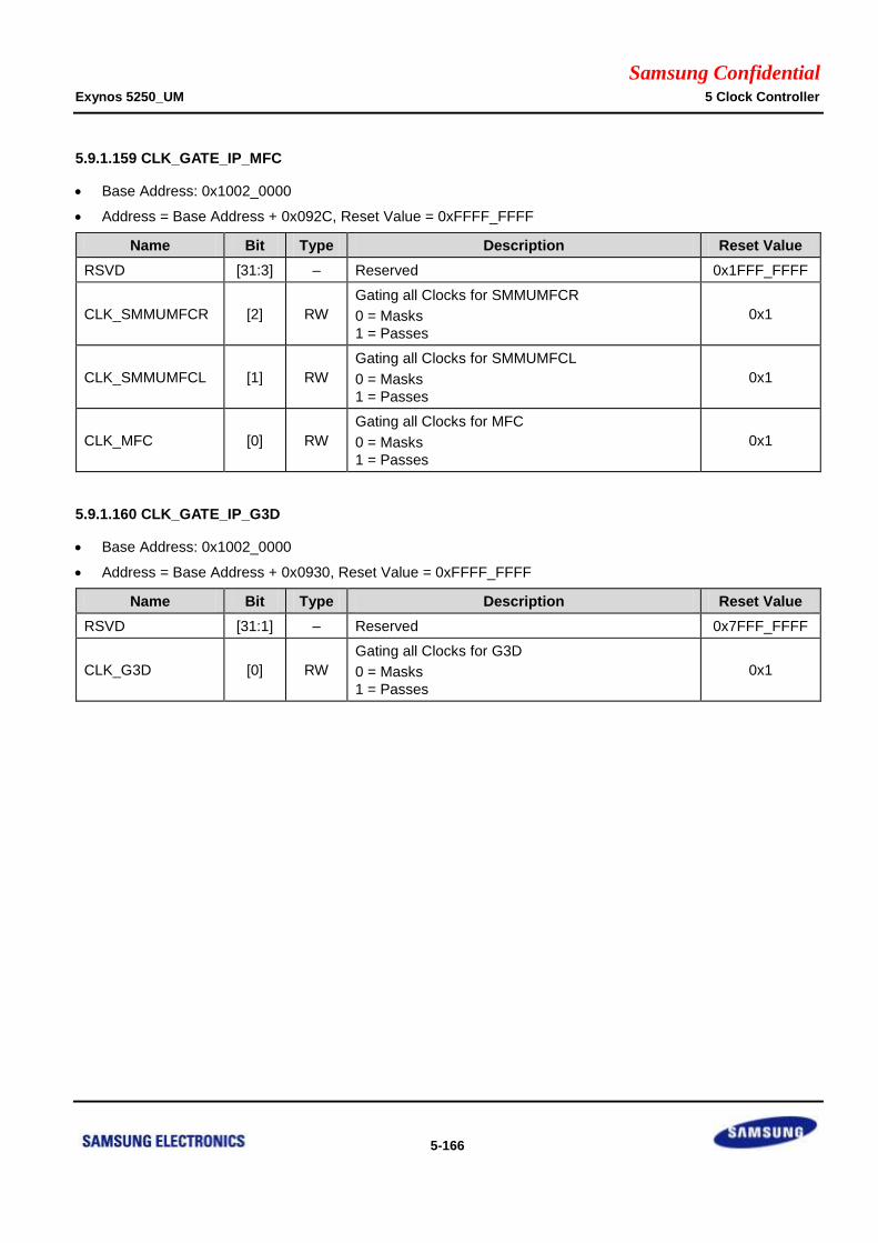
Samsung Confidential Exynos 5250_UM 5 Clock Controller
5-166
5.9.1.159 CLK_GATE_IP_MFC
Base Address: 0x1002_0000
Address = Base Address + 0x092C, Reset Value = 0xFFFF_FFFF
Name Bit Type Description Reset Value
RSVD [31:3] – Reserved 0x1FFF_FFFF
CLK_SMMUMFCR [2] RW
Gating all Clocks for SMMUMFCR
0 = Masks
1 = Passes
0x1
CLK_SMMUMFCL [1] RW
Gating all Clocks for SMMUMFCL
0 = Masks
1 = Passes
0x1
CLK_MFC [0] RW
Gating all Clocks for MFC
0 = Masks
1 = Passes
0x1
5.9.1.160 CLK_GATE_IP_G3D
Base Address: 0x1002_0000
Address = Base Address + 0x0930, Reset Value = 0xFFFF_FFFF
Name Bit Type Description Reset Value
RSVD [31:1] – Reserved 0x7FFF_FFFF
CLK_G3D [0] RW
Gating all Clocks for G3D
0 = Masks
1 = Passes
0x1

Samsung Confidential Exynos 5250_UM 5 Clock Controller
5-167
5.9.1.161 CLK_GATE_IP_GEN
Base Address: 0x1002_0000
Address = Base Address + 0x0934, Reset Value = 0xFFFF_FFFF
Name Bit Type Description Reset Value
RSVD [31:10] – Reserved 0x3F_FFFF
CLK
_SMMUMDMA1 [9] RW
Gating all Clocks for SMMUMDMA1
0 = Masks
1 = Passes
0x1
RSVD [8] – Reserved 0x1
CLK_SMMUJPEG [7] RW
Gating all Clocks for SMMUJPEG
0 = Masks
1 = Passes
0x1
CLK
_SMMUROTATOR [6] RW
Gating all Clocks for SMMUROTATOR
0 = Masks
1 = Passes
0x1
RSVD [5] – Reserved 0x1
CLK_MDMA1 [4] RW
Gating all Clocks for MDMA1
0 = Masks
1 = Passes
0x1
RSVD [3] – Reserved 0x1
CLK_JPEG [2] RW
Gating all Clocks for JPEG
0 = Masks
1 = Passes
0x1
CLK_ROTATOR [1] RW
Gating all Clocks for ROTATOR
0 = Masks
1 = Passes
0x1
RSVD [0] – Reserved 0x1
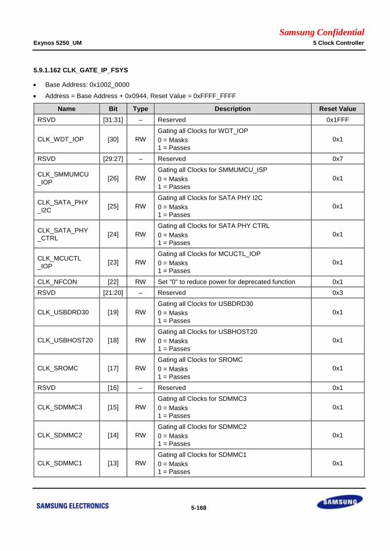
Samsung Confidential Exynos 5250_UM 5 Clock Controller
5-168
5.9.1.162 CLK_GATE_IP_FSYS
Base Address: 0x1002_0000
Address = Base Address + 0x0944, Reset Value = 0xFFFF_FFFF
Name Bit Type Description Reset Value
RSVD [31:31] – Reserved 0x1FFF
CLK_WDT_IOP [30] RW
Gating all Clocks for WDT_IOP
0 = Masks
1 = Passes
0x1
RSVD [29:27] – Reserved 0x7
CLK_SMMUMCU
_IOP [26] RW
Gating all Clocks for SMMUMCU_ISP
0 = Masks
1 = Passes
0x1
CLK_SATA_PHY
_I2C [25] RW
Gating all Clocks for SATA PHY I2C
0 = Masks
1 = Passes
0x1
CLK_SATA_PHY
_CTRL [24] RW
Gating all Clocks for SATA PHY CTRL
0 = Masks
1 = Passes
0x1
CLK_MCUCTL
_IOP [23] RW
Gating all Clocks for MCUCTL_IOP
0 = Masks
1 = Passes
0x1
CLK_NFCON [22] RW Set "0" to reduce power for deprecated function 0x1
RSVD [21:20] – Reserved 0x3
CLK_USBDRD30 [19] RW
Gating all Clocks for USBDRD30
0 = Masks
1 = Passes
0x1
CLK_USBHOST20 [18] RW
Gating all Clocks for USBHOST20
0 = Masks
1 = Passes
0x1
CLK_SROMC [17] RW
Gating all Clocks for SROMC
0 = Masks
1 = Passes
0x1
RSVD [16] – Reserved 0x1
CLK_SDMMC3 [15] RW
Gating all Clocks for SDMMC3
0 = Masks
1 = Passes
0x1
CLK_SDMMC2 [14] RW
Gating all Clocks for SDMMC2
0 = Masks
1 = Passes
0x1
CLK_SDMMC1 [13] RW
Gating all Clocks for SDMMC1
0 = Masks
1 = Passes
0x1
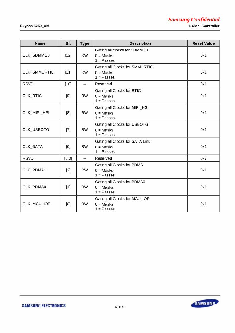
Samsung Confidential Exynos 5250_UM 5 Clock Controller
5-169
Name Bit Type Description Reset Value
CLK_SDMMC0 [12] RW
Gating all clocks for SDMMC0
0 = Masks
1 = Passes
0x1
CLK_SMMURTIC [11] RW
Gating all Clocks for SMMURTIC
0 = Masks
1 = Passes
0x1
RSVD [10] – Reserved 0x1
CLK_RTIC [9] RW
Gating all Clocks for RTIC
0 = Masks
1 = Passes
0x1
CLK_MIPI_HSI [8] RW
Gating all Clocks for MIPI_HSI
0 = Masks
1 = Passes
0x1
CLK_USBOTG [7] RW
Gating all Clocks for USBOTG
0 = Masks
1 = Passes
0x1
CLK_SATA [6] RW
Gating all Clocks for SATA Link
0 = Masks
1 = Passes
0x1
RSVD [5:3] – Reserved 0x7
CLK_PDMA1 [2] RW
Gating all Clocks for PDMA1
0 = Masks
1 = Passes
0x1
CLK_PDMA0 [1] RW
Gating all Clocks for PDMA0
0 = Masks
1 = Passes
0x1
CLK_MCU_IOP [0] RW
Gating all Clocks for MCU_IOP
0 = Masks
1 = Passes
0x1
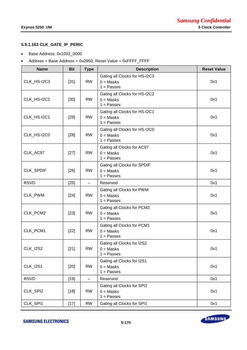
Samsung Confidential Exynos 5250_UM 5 Clock Controller
5-170
5.9.1.163 CLK_GATE_IP_PERIC
Base Address: 0x1002_0000
Address = Base Address + 0x0950, Reset Value = 0xFFFF_FFFF
Name Bit Type Description Reset Value
CLK_HS-I2C3 [31] RW
Gating all Clocks for HS-I2C3
0 = Masks
1 = Passes
0x1
CLK_HS-I2C2 [30] RW
Gating all Clocks for HS-I2C2
0 = Masks
1 = Passes
0x1
CLK_HS-I2C1 [29] RW
Gating all Clocks for HS-I2C1
0 = Masks
1 = Passes
0x1
CLK_HS-I2C0 [28] RW
Gating all Clocks for HS-I2C0
0 = Masks
1 = Passes
0x1
CLK_AC97 [27] RW
Gating all Clocks for AC97
0 = Masks
1 = Passes
0x1
CLK_SPDIF [26] RW
Gating all Clocks for SPDIF
0 = Masks
1 = Passes
0x1
RSVD [25] – Reserved 0x1
CLK_PWM [24] RW
Gating all Clocks for PWM
0 = Masks
1 = Passes
0x1
CLK_PCM2 [23] RW
Gating all Clocks for PCM2
0 = Masks
1 = Passes
0x1
CLK_PCM1 [22] RW
Gating all Clocks for PCM1
0 = Masks
1 = Passes
0x1
CLK_I2S2 [21] RW
Gating all Clocks for I2S2
0 = Masks
1 = Passes
0x1
CLK_I2S1 [20] RW
Gating all Clocks for I2S1
0 = Masks
1 = Passes
0x1
RSVD [19] – Reserved 0x1
CLK_SPI2 [18] RW
Gating all Clocks for SPI2
0 = Masks
1 = Passes
0x1
CLK_SPI1 [17] RW Gating all Clocks for SPI1 0x1
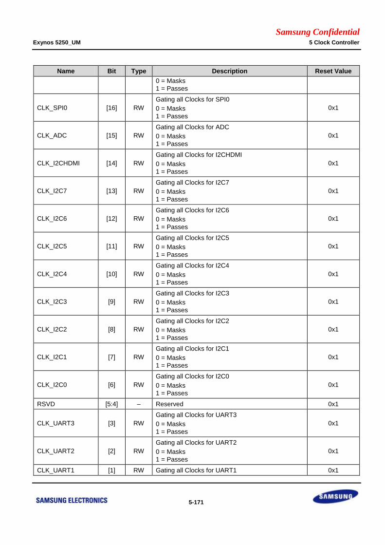
Samsung Confidential Exynos 5250_UM 5 Clock Controller
5-171
Name Bit Type Description Reset Value
0 = Masks
1 = Passes
CLK_SPI0 [16] RW
Gating all Clocks for SPI0
0 = Masks
1 = Passes
0x1
CLK_ADC [15] RW
Gating all Clocks for ADC
0 = Masks
1 = Passes
0x1
CLK_I2CHDMI [14] RW
Gating all Clocks for I2CHDMI
0 = Masks
1 = Passes
0x1
CLK_I2C7 [13] RW
Gating all Clocks for I2C7
0 = Masks
1 = Passes
0x1
CLK_I2C6 [12] RW
Gating all Clocks for I2C6
0 = Masks
1 = Passes
0x1
CLK_I2C5 [11] RW
Gating all Clocks for I2C5
0 = Masks
1 = Passes
0x1
CLK_I2C4 [10] RW
Gating all Clocks for I2C4
0 = Masks
1 = Passes
0x1
CLK_I2C3 [9] RW
Gating all Clocks for I2C3
0 = Masks
1 = Passes
0x1
CLK_I2C2 [8] RW
Gating all Clocks for I2C2
0 = Masks
1 = Passes
0x1
CLK_I2C1 [7] RW
Gating all Clocks for I2C1
0 = Masks
1 = Passes
0x1
CLK_I2C0 [6] RW
Gating all Clocks for I2C0
0 = Masks
1 = Passes
0x1
RSVD [5:4] – Reserved 0x1
CLK_UART3 [3] RW
Gating all Clocks for UART3
0 = Masks
1 = Passes
0x1
CLK_UART2 [2] RW
Gating all Clocks for UART2
0 = Masks
1 = Passes
0x1
CLK_UART1 [1] RW Gating all Clocks for UART1 0x1
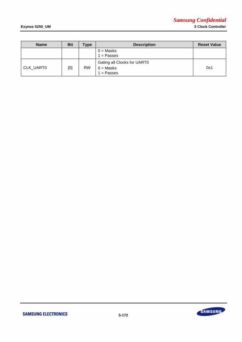
Samsung Confidential Exynos 5250_UM 5 Clock Controller
5-172
Name Bit Type Description Reset Value
0 = Masks
1 = Passes
CLK_UART0 [0] RW
Gating all Clocks for UART0
0 = Masks
1 = Passes
0x1

Samsung Confidential Exynos 5250_UM 5 Clock Controller
5-173
5.9.1.164 CLK_GATE_IP_PERIS
Base Address: 0x1002_0000
Address = Base Address + 0x0960, Reset Value = 0xFFFF_FFFF
Name Bit Type Description Reset Value
RSVD [31:25] – Reserved 0x3FFF
CLK_MONOCNT [24] RW
Gating all Clocks for Monotonic Counter
0 = Masks
1 = Passes
0x1
CLK_PKEY1 [23] RW
Gating all Clocks for Provision key 1
0 = Masks
1 = Passes
0x1
CLK_PKEY0 [22] RW
Gating all Clocks for Provision key 0
0 = Masks
1 = Passes
0x1
CLK_TMU_APBIF [21] RW
Gating all Clocks for TMU_APBIF
0 = Masks
1 = Passes
0x1
CLK_RTC [20] RW
Gating all Clocks for RTC
0 = Masks
1 = Passes
0x1
CLK_WDT [19] RW
Gating all Clocks for WDT
0 = Masks
1 = Passes
0x1
CLK_ST [18] RW
Gating all Clocks for ST
0 = Masks
1 = Passes
0x1
CLK_SECKEY
_APBIF [17] RW
Gating all Clocks for SECKEY_APBIF
0 = Masks
1 = Passes
0x1
CLK_HDMI_CEC [16] RW
Gating all Clocks for HDMI_CEC
0 = Masks
1 = Passes
0x1
CLK_TZPC9 [15] RW
Gating all Clocks for TZPC9
0 = Masks
1 = Passes
0x1
CLK_TZPC8 [14] RW
Gating all Clocks for TZPC8
0 = Masks
1 = Passes
0x1
CLK_TZPC7 [13] RW
Gating all Clocks for TZPC7
0 = Masks
1 = Passes
0x1
CLK_TZPC6 [12] RW Gating all Clocks for TZPC6
0 = Masks 0x1
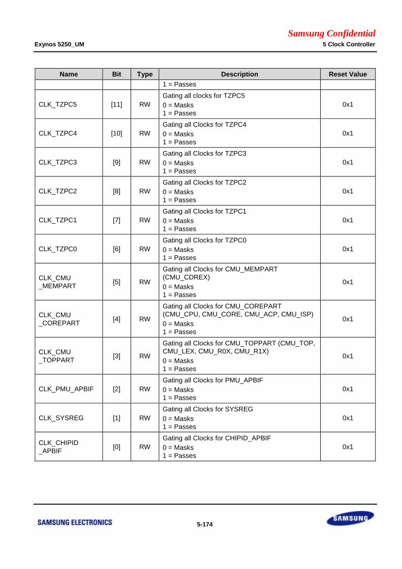
Samsung Confidential Exynos 5250_UM 5 Clock Controller
5-174
Name Bit Type Description Reset Value
1 = Passes
CLK_TZPC5 [11] RW
Gating all clocks for TZPC5
0 = Masks
1 = Passes
0x1
CLK_TZPC4 [10] RW
Gating all Clocks for TZPC4
0 = Masks
1 = Passes
0x1
CLK_TZPC3 [9] RW
Gating all Clocks for TZPC3
0 = Masks
1 = Passes
0x1
CLK_TZPC2 [8] RW
Gating all Clocks for TZPC2
0 = Masks
1 = Passes
0x1
CLK_TZPC1 [7] RW
Gating all Clocks for TZPC1
0 = Masks
1 = Passes
0x1
CLK_TZPC0 [6] RW
Gating all Clocks for TZPC0
0 = Masks
1 = Passes
0x1
CLK_CMU
_MEMPART [5] RW
Gating all Clocks for CMU_MEMPART
(CMU_CDREX)
0 = Masks
1 = Passes
0x1
CLK_CMU
_COREPART [4] RW
Gating all Clocks for CMU_COREPART
(CMU_CPU, CMU_CORE, CMU_ACP, CMU_ISP)
0 = Masks
1 = Passes
0x1
CLK_CMU
_TOPPART [3] RW
Gating all Clocks for CMU_TOPPART (CMU_TOP,
CMU_LEX, CMU_R0X, CMU_R1X)
0 = Masks
1 = Passes
0x1
CLK_PMU_APBIF [2] RW
Gating all Clocks for PMU_APBIF
0 = Masks
1 = Passes
0x1
CLK_SYSREG [1] RW
Gating all Clocks for SYSREG
0 = Masks
1 = Passes
0x1
CLK_CHIPID
_APBIF [0] RW
Gating all Clocks for CHIPID_APBIF
0 = Masks
1 = Passes
0x1
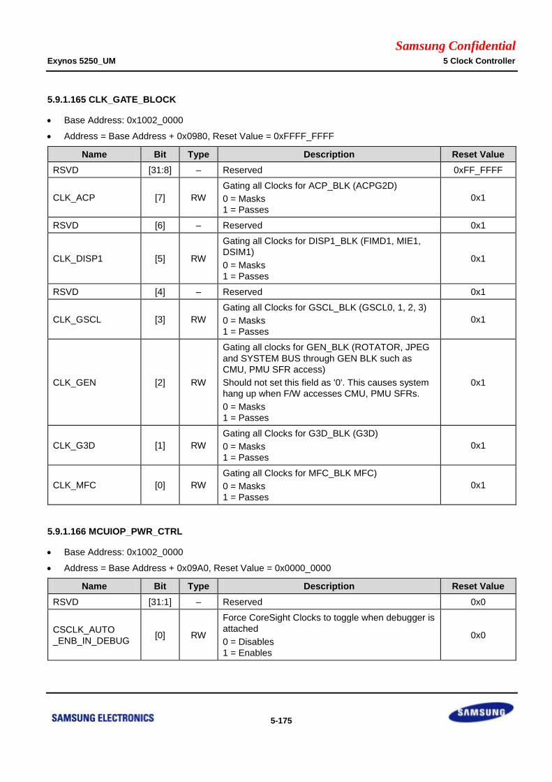
Samsung Confidential Exynos 5250_UM 5 Clock Controller
5-175
5.9.1.165 CLK_GATE_BLOCK
Base Address: 0x1002_0000
Address = Base Address + 0x0980, Reset Value = 0xFFFF_FFFF
Name Bit Type Description Reset Value
RSVD [31:8] – Reserved 0xFF_FFFF
CLK_ACP [7] RW
Gating all Clocks for ACP_BLK (ACPG2D)
0 = Masks
1 = Passes
0x1
RSVD [6] – Reserved 0x1
CLK_DISP1 [5] RW
Gating all Clocks for DISP1_BLK (FIMD1, MIE1,
DSIM1)
0 = Masks
1 = Passes
0x1
RSVD [4] – Reserved 0x1
CLK_GSCL [3] RW
Gating all Clocks for GSCL_BLK (GSCL0, 1, 2, 3)
0 = Masks
1 = Passes
0x1
CLK_GEN [2] RW
Gating all clocks for GEN_BLK (ROTATOR, JPEG
and SYSTEM BUS through GEN BLK such as
CMU, PMU SFR access)
Should not set this field as '0'. This causes system
hang up when F/W accesses CMU, PMU SFRs.
0 = Masks
1 = Passes
0x1
CLK_G3D [1] RW
Gating all Clocks for G3D_BLK (G3D)
0 = Masks
1 = Passes
0x1
CLK_MFC [0] RW
Gating all Clocks for MFC_BLK MFC)
0 = Masks
1 = Passes
0x1
5.9.1.166 MCUIOP_PWR_CTRL
Base Address: 0x1002_0000
Address = Base Address + 0x09A0, Reset Value = 0x0000_0000
Name Bit Type Description Reset Value
RSVD [31:1] – Reserved 0x0
CSCLK_AUTO
_ENB_IN_DEBUG [0] RW
Force CoreSight Clocks to toggle when debugger is
attached
0 = Disables
1 = Enables
0x0
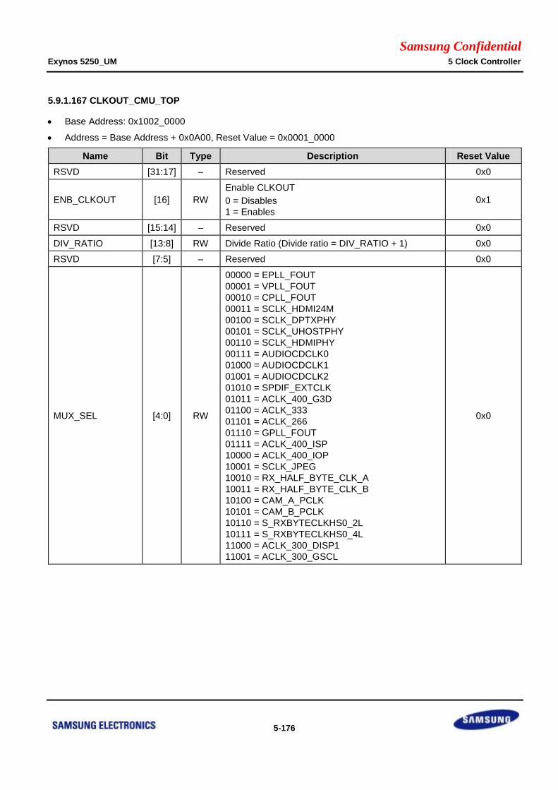
Samsung Confidential Exynos 5250_UM 5 Clock Controller
5-176
5.9.1.167 CLKOUT_CMU_TOP
Base Address: 0x1002_0000
Address = Base Address + 0x0A00, Reset Value = 0x0001_0000
Name Bit Type Description Reset Value
RSVD [31:17] – Reserved 0x0
ENB_CLKOUT [16] RW
Enable CLKOUT
0 = Disables
1 = Enables
0x1
RSVD [15:14] – Reserved 0x0
DIV_RATIO [13:8] RW Divide Ratio (Divide ratio = DIV_RATIO + 1) 0x0
RSVD [7:5] – Reserved 0x0
MUX_SEL [4:0] RW
00000 = EPLL_FOUT
00001 = VPLL_FOUT
00010 = CPLL_FOUT
00011 = SCLK_HDMI24M
00100 = SCLK_DPTXPHY
00101 = SCLK_UHOSTPHY
00110 = SCLK_HDMIPHY
00111 = AUDIOCDCLK0
01000 = AUDIOCDCLK1
01001 = AUDIOCDCLK2
01010 = SPDIF_EXTCLK
01011 = ACLK_400_G3D
01100 = ACLK_333
01101 = ACLK_266
01110 = GPLL_FOUT
01111 = ACLK_400_ISP
10000 = ACLK_400_IOP
10001 = SCLK_JPEG
10010 = RX_HALF_BYTE_CLK_A
10011 = RX_HALF_BYTE_CLK_B
10100 = CAM_A_PCLK
10101 = CAM_B_PCLK
10110 = S_RXBYTECLKHS0_2L
10111 = S_RXBYTECLKHS0_4L
11000 = ACLK_300_DISP1
11001 = ACLK_300_GSCL
0x0
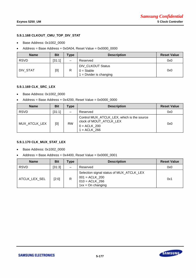
Samsung Confidential Exynos 5250_UM 5 Clock Controller
5-177
5.9.1.168 CLKOUT_CMU_TOP_DIV_STAT
Base Address: 0x1002_0000
Address = Base Address + 0x0A04, Reset Value = 0x0000_0000
Name Bit Type Description Reset Value
RSVD [31:1] – Reserved 0x0
DIV_STAT [0] R
DIV_CLKOUT Status
0 = Stable
1 = Divider is changing
0x0
5.9.1.169 CLK_SRC_LEX
Base Address: 0x1002_0000
Address = Base Address + 0x4200, Reset Value = 0x0000_0000
Name Bit Type Description Reset Value
RSVD [31:1] – Reserved 0x0
MUX_ATCLK_LEX [0] RW
Control MUX_ATCLK_LEX, which is the source
clock of MOUT_ATCLK_LEX
0 = ACLK_200
1 = ACLK_266
0x0
5.9.1.170 CLK_MUX_STAT_LEX
Base Address: 0x1002_0000
Address = Base Address + 0x4400, Reset Value = 0x0000_0001
Name Bit Type Description Reset Value
RSVD [31:3] – Reserved 0x0
ATCLK_LEX_SEL [2:0] R
Selection signal status of MUX_ATCLK_LEX
001 = ACLK_200
010 = ACLK_266
1xx = On changing
0x1
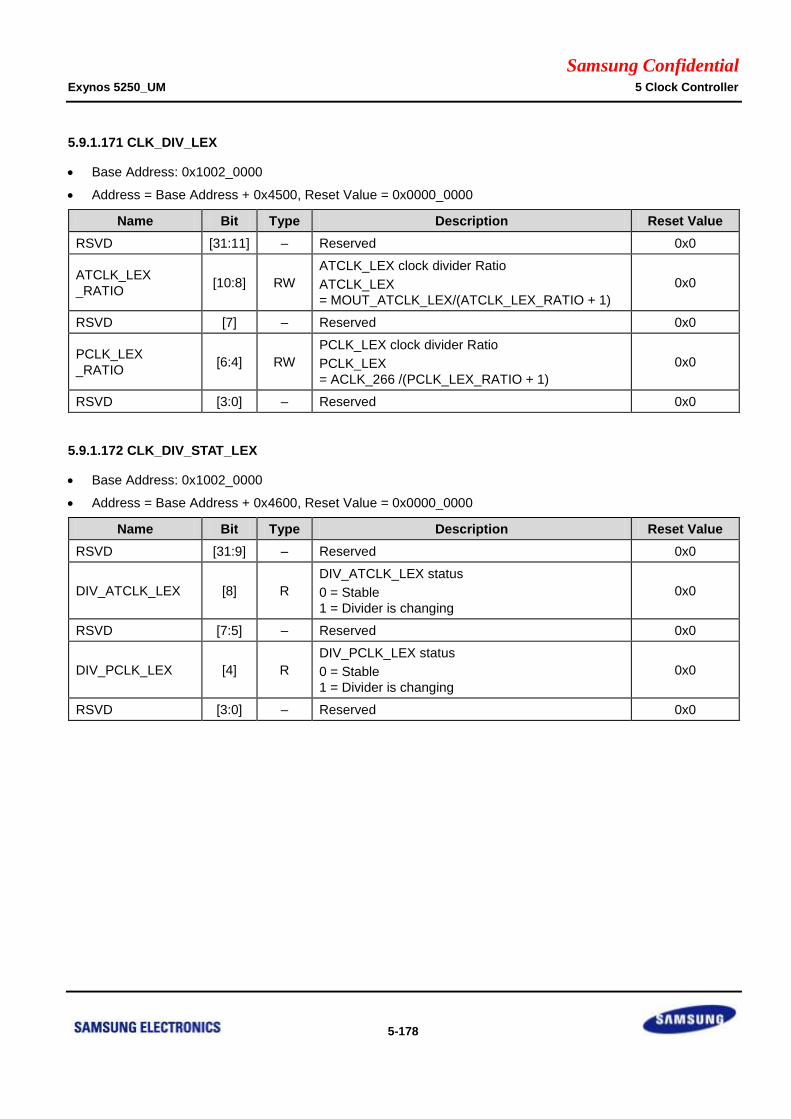
Samsung Confidential Exynos 5250_UM 5 Clock Controller
5-178
5.9.1.171 CLK_DIV_LEX
Base Address: 0x1002_0000
Address = Base Address + 0x4500, Reset Value = 0x0000_0000
Name Bit Type Description Reset Value
RSVD [31:11] – Reserved 0x0
ATCLK_LEX
_RATIO [10:8] RW
ATCLK_LEX clock divider Ratio
ATCLK_LEX
= MOUT_ATCLK_LEX/(ATCLK_LEX_RATIO + 1)
0x0
RSVD [7] – Reserved 0x0
PCLK_LEX
_RATIO [6:4] RW
PCLK_LEX clock divider Ratio
PCLK_LEX
= ACLK_266 /(PCLK_LEX_RATIO + 1)
0x0
RSVD [3:0] – Reserved 0x0
5.9.1.172 CLK_DIV_STAT_LEX
Base Address: 0x1002_0000
Address = Base Address + 0x4600, Reset Value = 0x0000_0000
Name Bit Type Description Reset Value
RSVD [31:9] – Reserved 0x0
DIV_ATCLK_LEX [8] R
DIV_ATCLK_LEX status
0 = Stable
1 = Divider is changing
0x0
RSVD [7:5] – Reserved 0x0
DIV_PCLK_LEX [4] R
DIV_PCLK_LEX status
0 = Stable
1 = Divider is changing
0x0
RSVD [3:0] – Reserved 0x0
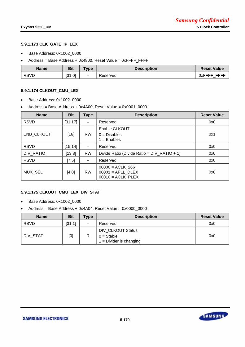
Samsung Confidential Exynos 5250_UM 5 Clock Controller
5-179
5.9.1.173 CLK_GATE_IP_LEX
Base Address: 0x1002_0000
Address = Base Address + 0x4800, Reset Value = 0xFFFF_FFFF
Name Bit Type Description Reset Value
RSVD [31:0] – Reserved 0xFFFF_FFFF
5.9.1.174 CLKOUT_CMU_LEX
Base Address: 0x1002_0000
Address = Base Address + 0x4A00, Reset Value = 0x0001_0000
Name Bit Type Description Reset Value
RSVD [31:17] – Reserved 0x0
ENB_CLKOUT [16] RW
Enable CLKOUT
0 = Disables
1 = Enables
0x1
RSVD [15:14] – Reserved 0x0
DIV_RATIO [13:8] RW Divide Ratio (Divide Ratio = DIV_RATIO + 1) 0x0
RSVD [7:5] – Reserved 0x0
MUX_SEL [4:0] RW
00000 = ACLK_266
00001 = APLL_DLEX
00010 = ACLK_PLEX
0x0
5.9.1.175 CLKOUT_CMU_LEX_DIV_STAT
Base Address: 0x1002_0000
Address = Base Address + 0x4A04, Reset Value = 0x0000_0000
Name Bit Type Description Reset Value
RSVD [31:1] – Reserved 0x0
DIV_STAT [0] R
DIV_CLKOUT Status
0 = Stable
1 = Divider is changing
0x0

Samsung Confidential Exynos 5250_UM 5 Clock Controller
5-180
5.9.1.176 CLK_DIV_R0X
Base Address: 0x1002_0000
Address = Base Address + 0x8500, Reset Value = 0x0000_0000
Name Bit Type Description Reset Value
RSVD [31:23] – Reserved 0x0
PCLK_R0X_RATIO [6:4] RW
DIV_PR0X Clock divider Ratio
PCLK_R0X
= ACLK_266/(PCLK_R0X_RATIO + 1)
0x0
RSVD [3:0] – Reserved 0x0
5.9.1.177 CLK_DIV_STAT_R0X
Base Address: 0x1002_0000
Address = Base Address + 0x8600, Reset Value = 0x0000_0000
Name Bit Type Description Reset Value
RSVD [31:5] – Reserved 0x0
DIV_PCLK_R0X [4] R
DIV_PR0X status
0 = Stable
1 = Divider is changing
0x0
RSVD [3:0] – Reserved 0x0
5.9.1.178 CLK_GATE_IP_R0X
Base Address: 0x1002_0000
Address = Base Address + 0x8800, Reset Value = 0xFFFF_FFFF
Name Bit Type Description Reset Value
RSVD [31:0] – Reserved 0xFFFF_FFFF
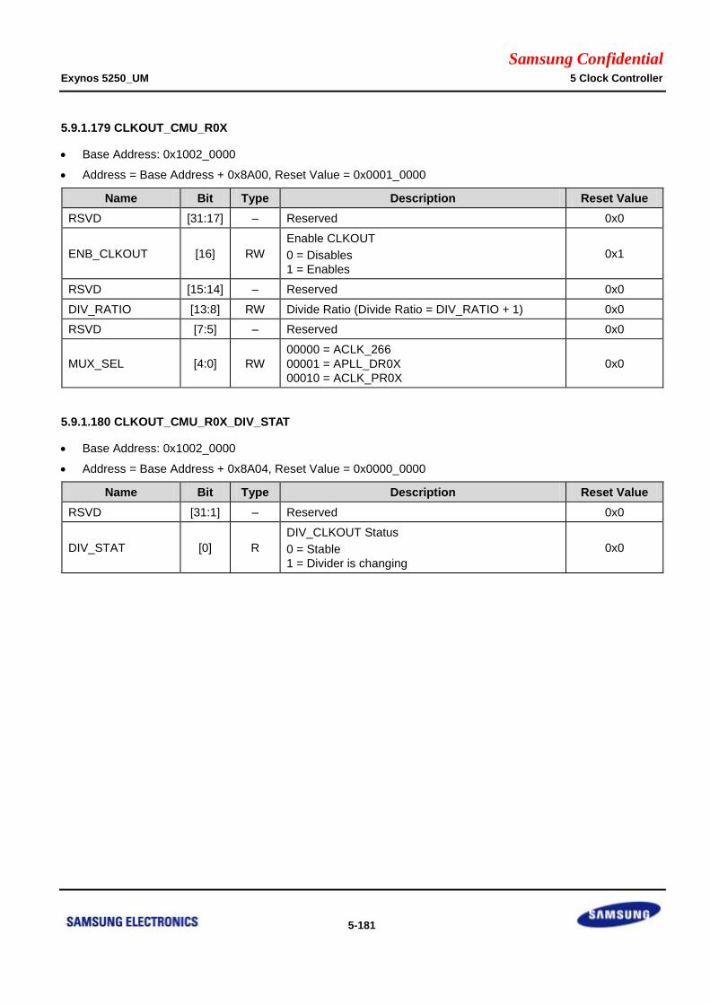
Samsung Confidential Exynos 5250_UM 5 Clock Controller
5-181
5.9.1.179 CLKOUT_CMU_R0X
Base Address: 0x1002_0000
Address = Base Address + 0x8A00, Reset Value = 0x0001_0000
Name Bit Type Description Reset Value
RSVD [31:17] – Reserved 0x0
ENB_CLKOUT [16] RW
Enable CLKOUT
0 = Disables
1 = Enables
0x1
RSVD [15:14] – Reserved 0x0
DIV_RATIO [13:8] RW Divide Ratio (Divide Ratio = DIV_RATIO + 1) 0x0
RSVD [7:5] – Reserved 0x0
MUX_SEL [4:0] RW
00000 = ACLK_266
00001 = APLL_DR0X
00010 = ACLK_PR0X
0x0
5.9.1.180 CLKOUT_CMU_R0X_DIV_STAT
Base Address: 0x1002_0000
Address = Base Address + 0x8A04, Reset Value = 0x0000_0000
Name Bit Type Description Reset Value
RSVD [31:1] – Reserved 0x0
DIV_STAT [0] R
DIV_CLKOUT Status
0 = Stable
1 = Divider is changing
0x0
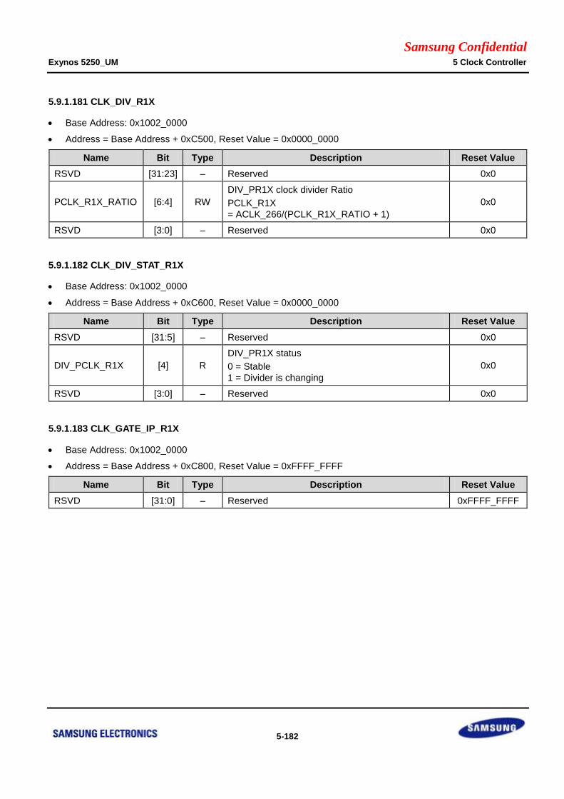
Samsung Confidential Exynos 5250_UM 5 Clock Controller
5-182
5.9.1.181 CLK_DIV_R1X
Base Address: 0x1002_0000
Address = Base Address + 0xC500, Reset Value = 0x0000_0000
Name Bit Type Description Reset Value
RSVD [31:23] – Reserved 0x0
PCLK_R1X_RATIO [6:4] RW
DIV_PR1X clock divider Ratio
PCLK_R1X
= ACLK_266/(PCLK_R1X_RATIO + 1)
0x0
RSVD [3:0] – Reserved 0x0
5.9.1.182 CLK_DIV_STAT_R1X
Base Address: 0x1002_0000
Address = Base Address + 0xC600, Reset Value = 0x0000_0000
Name Bit Type Description Reset Value
RSVD [31:5] – Reserved 0x0
DIV_PCLK_R1X [4] R
DIV_PR1X status
0 = Stable
1 = Divider is changing
0x0
RSVD [3:0] – Reserved 0x0
5.9.1.183 CLK_GATE_IP_R1X
Base Address: 0x1002_0000
Address = Base Address + 0xC800, Reset Value = 0xFFFF_FFFF
Name Bit Type Description Reset Value
RSVD [31:0] – Reserved 0xFFFF_FFFF
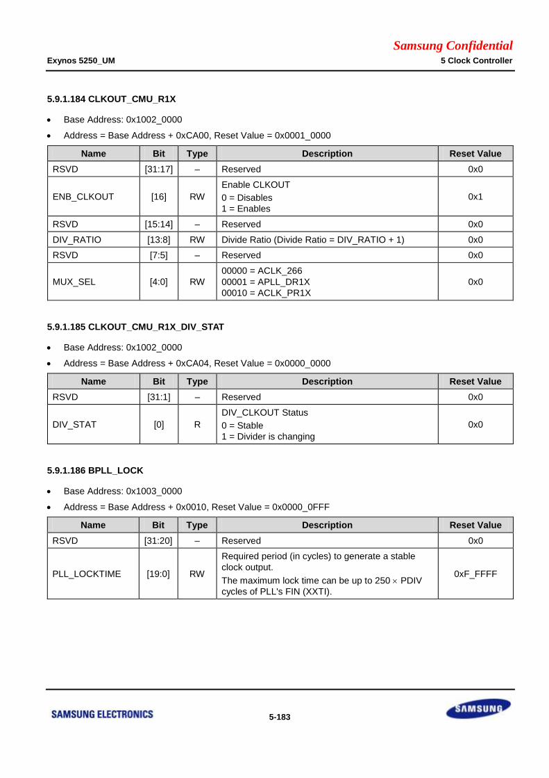
Samsung Confidential Exynos 5250_UM 5 Clock Controller
5-183
5.9.1.184 CLKOUT_CMU_R1X
Base Address: 0x1002_0000
Address = Base Address + 0xCA00, Reset Value = 0x0001_0000
Name Bit Type Description Reset Value
RSVD [31:17] – Reserved 0x0
ENB_CLKOUT [16] RW
Enable CLKOUT
0 = Disables
1 = Enables
0x1
RSVD [15:14] – Reserved 0x0
DIV_RATIO [13:8] RW Divide Ratio (Divide Ratio = DIV_RATIO + 1) 0x0
RSVD [7:5] – Reserved 0x0
MUX_SEL [4:0] RW
00000 = ACLK_266
00001 = APLL_DR1X
00010 = ACLK_PR1X
0x0
5.9.1.185 CLKOUT_CMU_R1X_DIV_STAT
Base Address: 0x1002_0000
Address = Base Address + 0xCA04, Reset Value = 0x0000_0000
Name Bit Type Description Reset Value
RSVD [31:1] – Reserved 0x0
DIV_STAT [0] R
DIV_CLKOUT Status
0 = Stable
1 = Divider is changing
0x0
5.9.1.186 BPLL_LOCK
Base Address: 0x1003_0000
Address = Base Address + 0x0010, Reset Value = 0x0000_0FFF
Name Bit Type Description Reset Value
RSVD [31:20] – Reserved 0x0
PLL_LOCKTIME [19:0] RW
Required period (in cycles) to generate a stable
clock output.
The maximum lock time can be up to 250 PDIV
cycles of PLL's FIN (XXTI).
0xF_FFFF
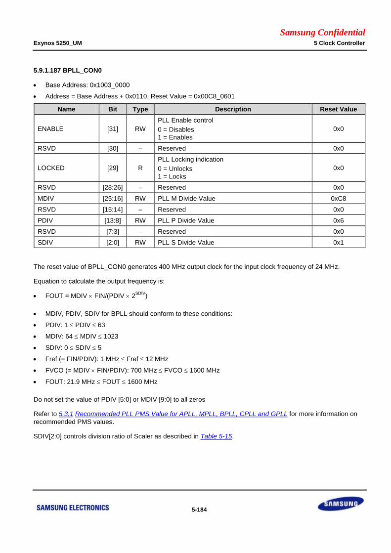
Samsung Confidential Exynos 5250_UM 5 Clock Controller
5-184
5.9.1.187 BPLL_CON0
Base Address: 0x1003_0000
Address = Base Address + 0x0110, Reset Value = 0x00C8_0601
Name Bit Type Description Reset Value
ENABLE [31] RW
PLL Enable control
0 = Disables
1 = Enables
0x0
RSVD [30] – Reserved 0x0
LOCKED [29] R
PLL Locking indication
0 = Unlocks
1 = Locks
0x0
RSVD [28:26] – Reserved 0x0
MDIV [25:16] RW PLL M Divide Value 0xC8
RSVD [15:14] – Reserved 0x0
PDIV [13:8] RW PLL P Divide Value 0x6
RSVD [7:3] – Reserved 0x0
SDIV [2:0] RW PLL S Divide Value 0x1
The reset value of BPLL_CON0 generates 400 MHz output clock for the input clock frequency of 24 MHz.
Equation to calculate the output frequency is:
FOUT = MDIV FIN/(PDIV 2SDIV
)
MDIV, PDIV, SDIV for BPLL should conform to these conditions:
PDIV: 1 PDIV 63
MDIV: 64 MDIV 1023
SDIV: 0 SDIV 5
Fref (= FIN/PDIV): 1 MHz Fref 12 MHz
FVCO (= MDIV FIN/PDIV): 700 MHz FVCO 1600 MHz
FOUT: 21.9 MHz FOUT 1600 MHz
Do not set the value of PDIV [5:0] or MDIV [9:0] to all zeros
Refer to 5.3.1 Recommended PLL PMS Value for APLL, MPLL, BPLL, CPLL and GPLL for more information on
recommended PMS values.
SDIV[2:0] controls division ratio of Scaler as described in Table 5-15.
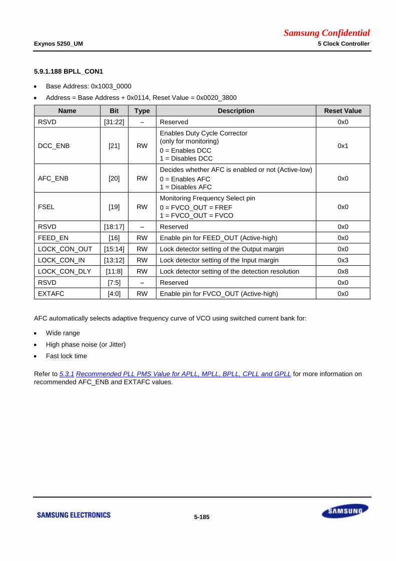
Samsung Confidential Exynos 5250_UM 5 Clock Controller
5-185
5.9.1.188 BPLL_CON1
Base Address: 0x1003_0000
Address = Base Address + 0x0114, Reset Value = 0x0020_3800
Name Bit Type Description Reset Value
RSVD [31:22] – Reserved 0x0
DCC_ENB [21] RW
Enables Duty Cycle Corrector
(only for monitoring)
0 = Enables DCC
1 = Disables DCC
0x1
AFC_ENB [20] RW
Decides whether AFC is enabled or not (Active-low)
0 = Enables AFC
1 = Disables AFC
0x0
FSEL [19] RW
Monitoring Frequency Select pin
0 = FVCO_OUT = FREF
1 = FVCO_OUT = FVCO
0x0
RSVD [18:17] – Reserved 0x0
FEED_EN [16] RW Enable pin for FEED_OUT (Active-high) 0x0
LOCK_CON_OUT [15:14] RW Lock detector setting of the Output margin 0x0
LOCK_CON_IN [13:12] RW Lock detector setting of the Input margin 0x3
LOCK_CON_DLY [11:8] RW Lock detector setting of the detection resolution 0x8
RSVD [7:5] – Reserved 0x0
EXTAFC [4:0] RW Enable pin for FVCO_OUT (Active-high) 0x0
AFC automatically selects adaptive frequency curve of VCO using switched current bank for:
Wide range
High phase noise (or Jitter)
Fast lock time
Refer to 5.3.1 Recommended PLL PMS Value for APLL, MPLL, BPLL, CPLL and GPLL for more information on
recommended AFC_ENB and EXTAFC values.
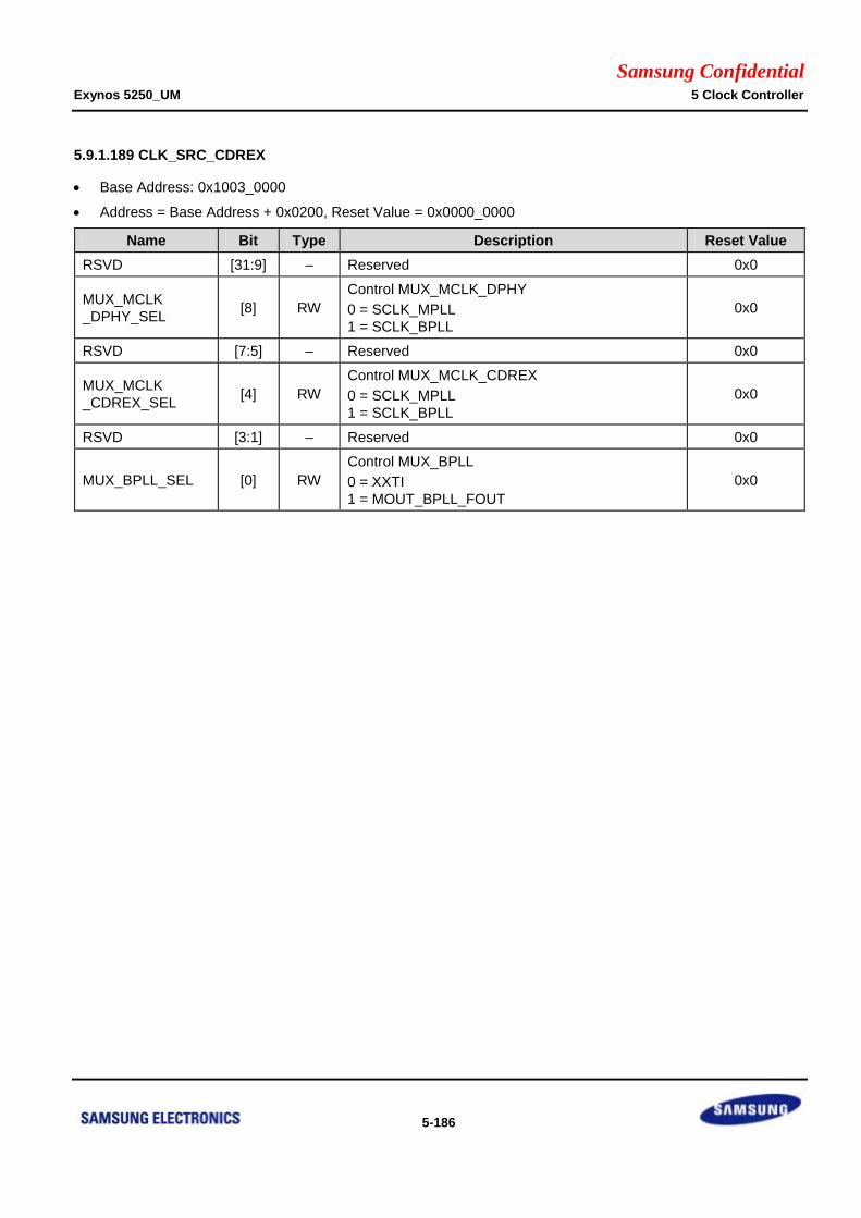
Samsung Confidential Exynos 5250_UM 5 Clock Controller
5-186
5.9.1.189 CLK_SRC_CDREX
Base Address: 0x1003_0000
Address = Base Address + 0x0200, Reset Value = 0x0000_0000
Name Bit Type Description Reset Value
RSVD [31:9] – Reserved 0x0
MUX_MCLK
_DPHY_SEL [8] RW
Control MUX_MCLK_DPHY
0 = SCLK_MPLL
1 = SCLK_BPLL
0x0
RSVD [7:5] – Reserved 0x0
MUX_MCLK
_CDREX_SEL [4] RW
Control MUX_MCLK_CDREX
0 = SCLK_MPLL
1 = SCLK_BPLL
0x0
RSVD [3:1] – Reserved 0x0
MUX_BPLL_SEL [0] RW
Control MUX_BPLL
0 = XXTI
1 = MOUT_BPLL_FOUT
0x0
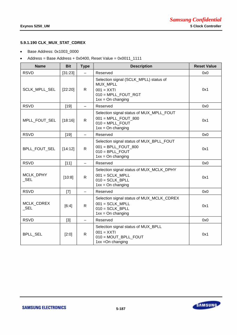
Samsung Confidential Exynos 5250_UM 5 Clock Controller
5-187
5.9.1.190 CLK_MUX_STAT_CDREX
Base Address: 0x1003_0000
Address = Base Address + 0x0400, Reset Value = 0x0011_1111
Name Bit Type Description Reset Value
RSVD [31:23] – Reserved 0x0
SCLK_MPLL_SEL [22:20] R
Selection signal (SCLK_MPLL) status of
MUX_MPLL
001 = XXTI
010 = MPLL_FOUT_RGT
1xx = On changing
0x1
RSVD [19] – Reserved 0x0
MPLL_FOUT_SEL [18:16] R
Selection signal status of MUX_MPLL_FOUT
001 = MPLL_FOUT_800
010 = MPLL_FOUT
1xx = On changing
0x1
RSVD [19] – Reserved 0x0
BPLL_FOUT_SEL [14:12] R
Selection signal status of MUX_BPLL_FOUT
001 = BPLL_FOUT_800
010 = BPLL_FOUT
1xx = On changing
0x1
RSVD [11] – Reserved 0x0
MCLK_DPHY
_SEL [10:8] R
Selection signal status of MUX_MCLK_DPHY
001 = SCLK_MPLL
010 = SCLK_BPLL
1xx = On changing
0x1
RSVD [7] – Reserved 0x0
MCLK_CDREX
_SEL [6:4] R
Selection signal status of MUX_MCLK_CDREX
001 = SCLK_MPLL
010 = SCLK_BPLL
1xx = On changing
0x1
RSVD [3] – Reserved 0x0
BPLL_SEL [2:0] R
Selection signal status of MUX_BPLL
001 = XXTI
010 = MOUT_BPLL_FOUT
1xx =On changing
0x1
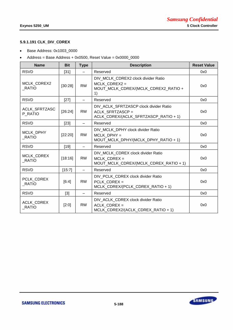
Samsung Confidential Exynos 5250_UM 5 Clock Controller
5-188
5.9.1.191 CLK_DIV_CDREX
Base Address: 0x1003_0000
Address = Base Address + 0x0500, Reset Value = 0x0000_0000
Name Bit Type Description Reset Value
RSVD [31] – Reserved 0x0
MCLK_CDREX2
_RATIO [30:28] RW
DIV_MCLK_CDREX2 clock divider Ratio
MCLK_CDREX2 =
MOUT_MCLK_CDREX/(MCLK_CDREX2_RATIO +
1)
0x0
RSVD [27] – Reserved 0x0
ACLK_SFRTZASC
P_RATIO [26:24] RW
DIV_ACLK_SFRTZASCP clock divider Ratio
ACLK_SFRTZASCP =
ACLK_CDREX/(ACLK_SFRTZASCP_RATIO + 1)
0x0
RSVD [23] – Reserved 0x0
MCLK_DPHY
_RATIO [22:20] RW
DIV_MCLK_DPHY clock divider Ratio
MCLK_DPHY =
MOUT_MCLK_DPHY/(MCLK_DPHY_RATIO + 1)
0x0
RSVD [19] – Reserved 0x0
MCLK_CDREX
_RATIO [18:16] RW
DIV_MCLK_CDREX clock divider Ratio
MCLK_CDREX =
MOUT_MCLK_CDREX/(MCLK_CDREX_RATIO + 1)
0x0
RSVD [15:7] – Reserved 0x0
PCLK_CDREX
_RATIO [6:4] RW
DIV_PCLK_CDREX clock divider Ratio
PCLK_CDREX =
MCLK_CDREX/(PCLK_CDREX_RATIO + 1)
0x0
RSVD [3] – Reserved 0x0
ACLK_CDREX
_RATIO [2:0] RW
DIV_ACLK_CDREX clock divider Ratio
ACLK_CDREX =
MCLK_CDREX2/(ACLK_CDREX_RATIO + 1)
0x0
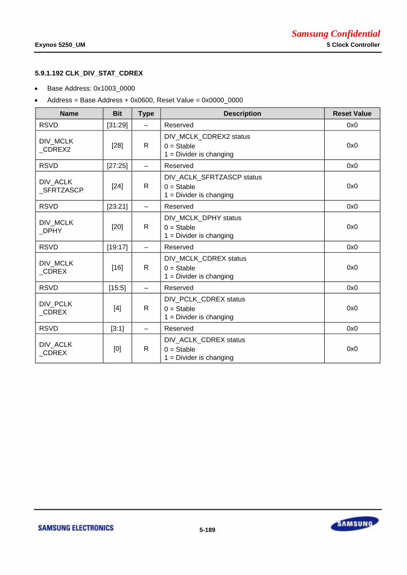
Samsung Confidential Exynos 5250_UM 5 Clock Controller
5-189
5.9.1.192 CLK_DIV_STAT_CDREX
Base Address: 0x1003_0000
Address = Base Address + 0x0600, Reset Value = 0x0000_0000
Name Bit Type Description Reset Value
RSVD [31:29] – Reserved 0x0
DIV_MCLK
_CDREX2 [28] R
DIV_MCLK_CDREX2 status
0 = Stable
1 = Divider is changing
0x0
RSVD [27:25] – Reserved 0x0
DIV_ACLK
_SFRTZASCP [24] R
DIV_ACLK_SFRTZASCP status
0 = Stable
1 = Divider is changing
0x0
RSVD [23:21] – Reserved 0x0
DIV_MCLK
_DPHY [20] R
DIV_MCLK_DPHY status
0 = Stable
1 = Divider is changing
0x0
RSVD [19:17] – Reserved 0x0
DIV_MCLK
_CDREX [16] R
DIV_MCLK_CDREX status
0 = Stable
1 = Divider is changing
0x0
RSVD [15:5] – Reserved 0x0
DIV_PCLK
_CDREX [4] R
DIV_PCLK_CDREX status
0 = Stable
1 = Divider is changing
0x0
RSVD [3:1] – Reserved 0x0
DIV_ACLK
_CDREX [0] R
DIV_ACLK_CDREX status
0 = Stable
1 = Divider is changing
0x0

Samsung Confidential Exynos 5250_UM 5 Clock Controller
5-190
5.9.1.193 CLK_GATE_IP_CDREX
Base Address: 0x1003_0000
Address = Base Address + 0x0900, Reset Value = 0xFFFF_FFFF
Name Bit Type Description Reset Value
RSVD [31:26] – Reserved 0x3F
CLK_TZASC
_CBXW [25] RW
Gating AXI Clock for TZASC_XCBXW and DRAM
controller port1
0 = Masks
1 = Passes
0x1
CLK_TZASC
_CBXR [24] RW
Gating AXI Clock for TZASC_XCBXR
0 = Masks
1 = Passes
0x1
CLK_TZASC
_DRBXW [23] RW
Gating AXI Clock for TZASC_XDRBXW and DRAM
controller port3
0 = Masks
1 = Passes
0x1
CLK_TZASC
_DRBXR [22] RW
Gating AXI Clock for TZASC_XDRBXR
0 = Masks
1 = Passes
0x1
CLK_TZASC
_XLBXW [21] RW
Gating AXI clock for TZASC_XLBXW and DRAM
controller port0
0 = Masks
1 = Passes
0x1
CLK_TZASC
_XLBXR [20] RW
Gating AXI clock for TZASC_XLBXR
0 = Masks
1 = Passes
0x1
CLK_TZASC
_XR1BXW [19] RW
Gating AXI clock for TZASC_XR1BXW and DRAM
controller port2
0 = Masks
1 = Passes
0x1
CLK_TZASC
_XR1BXR [18] RW
Gating AXI clock for TZASC_XR1BXR
0 = Masks
1 = Passes
0x1
RSVD [17:7] – Reserved 0x1FFF
CLK
_SFRTZASCP [6] RW
Gating all Clocks for AXI2APB_TZASCP and
AXI_CNVSX
0 = Masks
1 = Passes
0x1
CLK_DPHY1 [5] RW
Gating DLL Clocks for LPDDRHPHY1
0 = Masks
1 = Passes
0x1
CLK_DPHY0 [4] RW
Gating DLL Clocks for LPDDRHPHY0
0 = Masks
1 = Passes
0x1
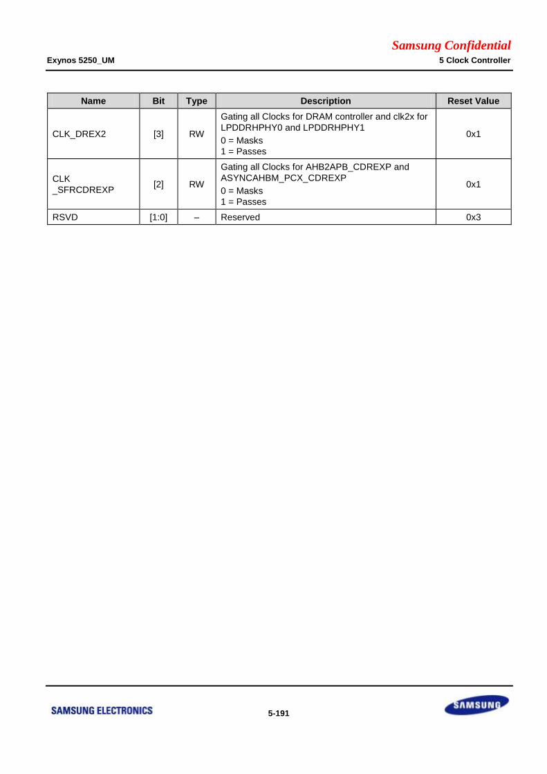
Samsung Confidential Exynos 5250_UM 5 Clock Controller
5-191
Name Bit Type Description Reset Value
CLK_DREX2 [3] RW
Gating all Clocks for DRAM controller and clk2x for
LPDDRHPHY0 and LPDDRHPHY1
0 = Masks
1 = Passes
0x1
CLK
_SFRCDREXP [2] RW
Gating all Clocks for AHB2APB_CDREXP and
ASYNCAHBM_PCX_CDREXP
0 = Masks
1 = Passes
0x1
RSVD [1:0] – Reserved 0x3
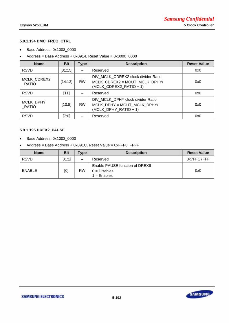
Samsung Confidential Exynos 5250_UM 5 Clock Controller
5-192
5.9.1.194 DMC_FREQ_CTRL
Base Address: 0x1003_0000
Address = Base Address + 0x0914, Reset Value = 0x0000_0000
Name Bit Type Description Reset Value
RSVD [31:15] – Reserved 0x0
MCLK_CDREX2
_RATIO [14:12] RW
DIV_MCLK_CDREX2 clock divider Ratio
MCLK_CDREX2 = MOUT_MCLK_DPHY/
(MCLK_CDREX2_RATIO + 1)
0x0
RSVD [11] – Reserved 0x0
MCLK_DPHY
_RATIO [10:8] RW
DIV_MCLK_DPHY clock divider Ratio
MCLK_DPHY = MOUT_MCLK_DPHY/
(MCLK_DPHY_RATIO + 1)
0x0
RSVD [7:0] – Reserved 0x0
5.9.1.195 DREX2_PAUSE
Base Address: 0x1003_0000
Address = Base Address + 0x091C, Reset Value = 0xFFF8_FFFF
Name Bit Type Description Reset Value
RSVD [31:1] – Reserved 0x7FFC7FFF
ENABLE [0] RW
Enable PAUSE function of DREXII
0 = Disables
1 = Enables
0x0
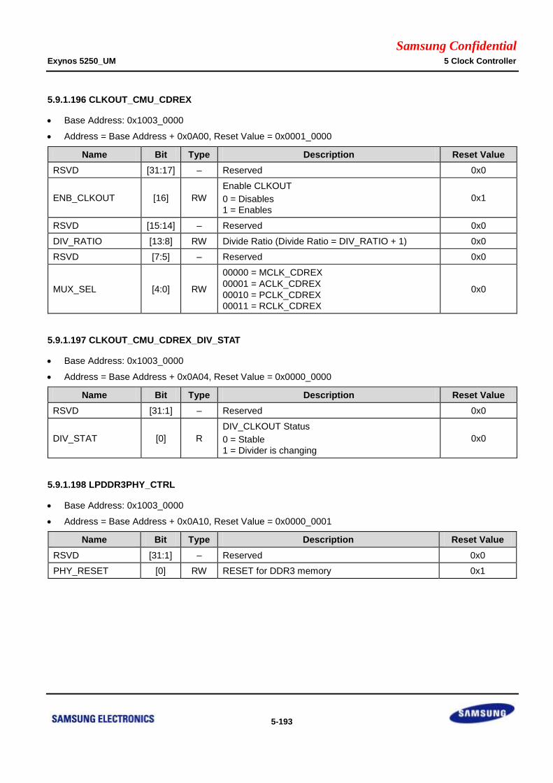
Samsung Confidential Exynos 5250_UM 5 Clock Controller
5-193
5.9.1.196 CLKOUT_CMU_CDREX
Base Address: 0x1003_0000
Address = Base Address + 0x0A00, Reset Value = 0x0001_0000
Name Bit Type Description Reset Value
RSVD [31:17] – Reserved 0x0
ENB_CLKOUT [16] RW
Enable CLKOUT
0 = Disables
1 = Enables
0x1
RSVD [15:14] – Reserved 0x0
DIV_RATIO [13:8] RW Divide Ratio (Divide Ratio = DIV_RATIO + 1) 0x0
RSVD [7:5] – Reserved 0x0
MUX_SEL [4:0] RW
00000 = MCLK_CDREX
00001 = ACLK_CDREX
00010 = PCLK_CDREX
00011 = RCLK_CDREX
0x0
5.9.1.197 CLKOUT_CMU_CDREX_DIV_STAT
Base Address: 0x1003_0000
Address = Base Address + 0x0A04, Reset Value = 0x0000_0000
Name Bit Type Description Reset Value
RSVD [31:1] – Reserved 0x0
DIV_STAT [0] R
DIV_CLKOUT Status
0 = Stable
1 = Divider is changing
0x0
5.9.1.198 LPDDR3PHY_CTRL
Base Address: 0x1003_0000
Address = Base Address + 0x0A10, Reset Value = 0x0000_0001
Name Bit Type Description Reset Value
RSVD [31:1] – Reserved 0x0
PHY_RESET [0] RW RESET for DDR3 memory 0x1
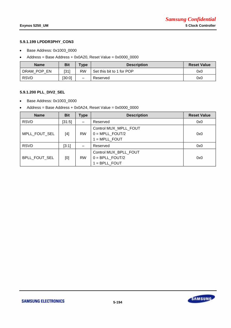
Samsung Confidential Exynos 5250_UM 5 Clock Controller
5-194
5.9.1.199 LPDDR3PHY_CON3
Base Address: 0x1003_0000
Address = Base Address + 0x0A20, Reset Value = 0x0000_0000
Name Bit Type Description Reset Value
DRAM_POP_EN [31] RW Set this bit to 1 for POP 0x0
RSVD [30:0] – Reserved 0x0
5.9.1.200 PLL_DIV2_SEL
Base Address: 0x1003_0000
Address = Base Address + 0x0A24, Reset Value = 0x0000_0000
Name Bit Type Description Reset Value
RSVD [31:5] – Reserved 0x0
MPLL_FOUT_SEL [4] RW
Control MUX_MPLL_FOUT
0 = MPLL_FOUT/2
1 = MPLL_FOUT
0x0
RSVD [3:1] – Reserved 0x0
BPLL_FOUT_SEL [0] RW
Control MUX_BPLL_FOUT
0 = BPLL_FOUT/2
1 = BPLL_FOUT
0x0
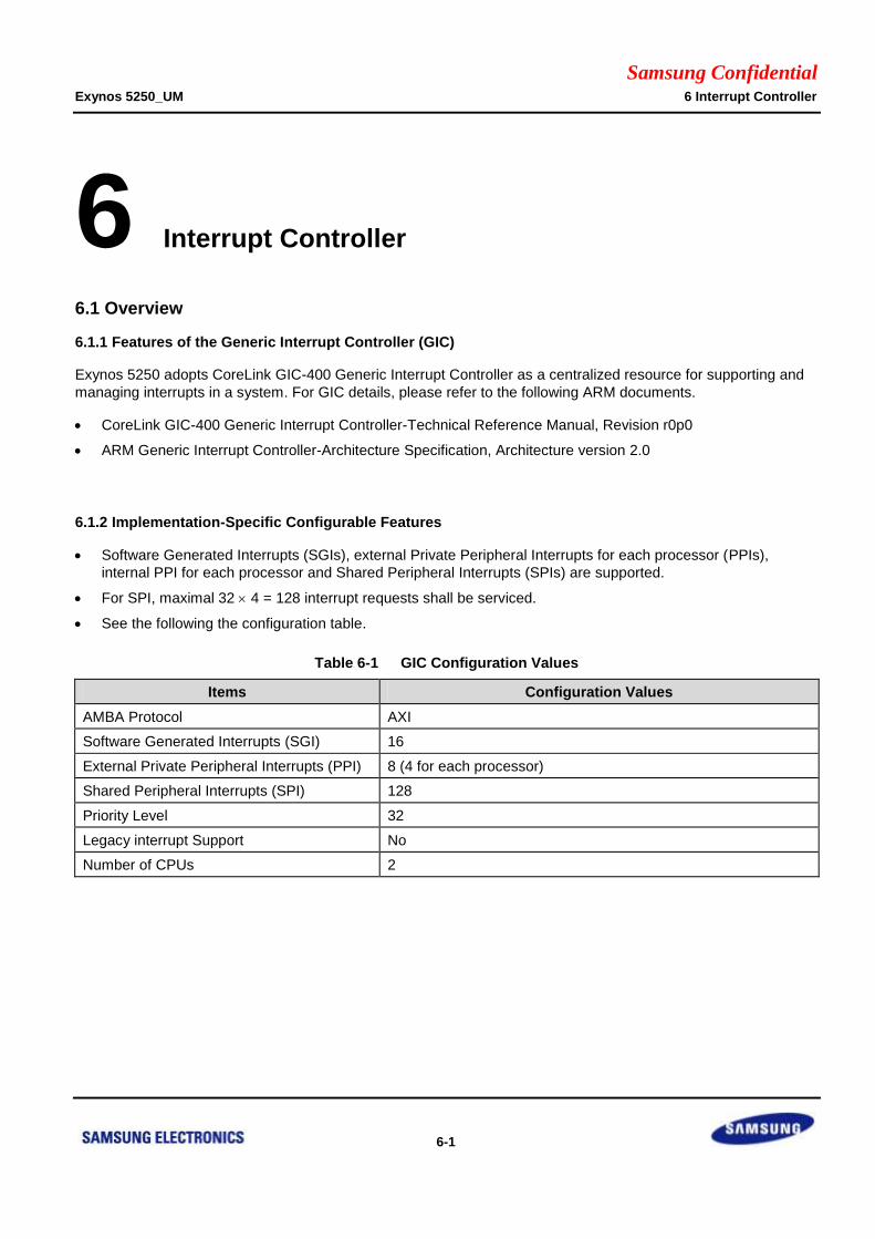
Samsung Confidential Exynos 5250_UM 6 Interrupt Controller
6-1
6 Interrupt Controller
6.1 Overview
6.1.1 Features of the Generic Interrupt Controller (GIC)
Exynos 5250 adopts CoreLink GIC-400 Generic Interrupt Controller as a centralized resource for supporting and
managing interrupts in a system. For GIC details, please refer to the following ARM documents.
CoreLink GIC-400 Generic Interrupt Controller-Technical Reference Manual, Revision r0p0
ARM Generic Interrupt Controller-Architecture Specification, Architecture version 2.0
6.1.2 Implementation-Specific Configurable Features
Software Generated Interrupts (SGIs), external Private Peripheral Interrupts for each processor (PPIs),
internal PPI for each processor and Shared Peripheral Interrupts (SPIs) are supported.
For SPI, maximal 32 4 = 128 interrupt requests shall be serviced.
See the following the configuration table.
Table 6-1 GIC Configuration Values
Items Configuration Values
AMBA Protocol AXI
Software Generated Interrupts (SGI) 16
External Private Peripheral Interrupts (PPI) 8 (4 for each processor)
Shared Peripheral Interrupts (SPI) 128
Priority Level 32
Legacy interrupt Support No
Number of CPUs 2
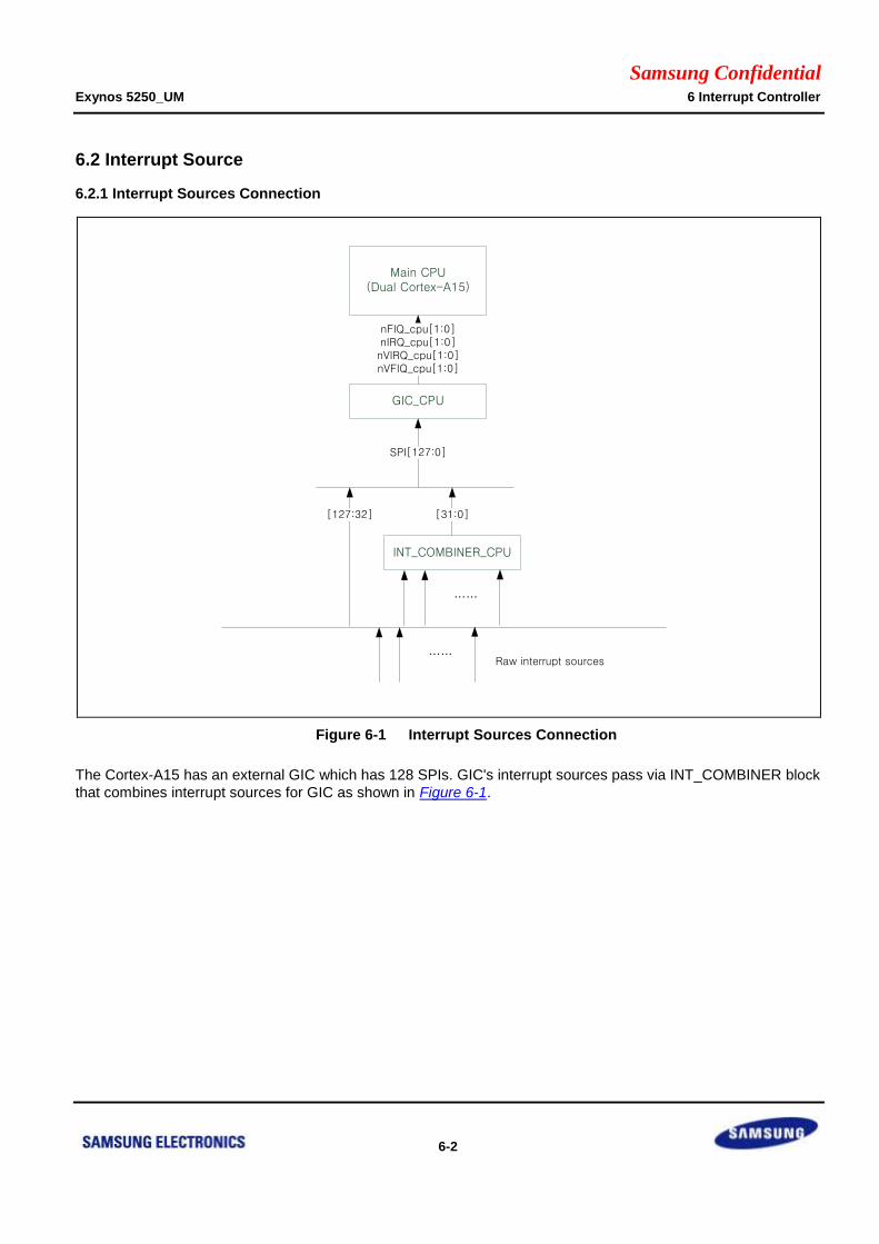
Samsung Confidential Exynos 5250_UM 6 Interrupt Controller
6-2
6.2 Interrupt Source
6.2.1 Interrupt Sources Connection
Main CPU(Dual Cortex-A15)
GIC_CPU
INT_COMBINER_CPU
nFIQ_cpu[1:0]nIRQ_cpu[1:0]nVIRQ_cpu[1:0]nVFIQ_cpu[1:0]
[31:0]
……
[127:32]
SPI[127:0]
…… Raw interrupt sources
Figure 6-1 Interrupt Sources Connection
The Cortex-A15 has an external GIC which has 128 SPIs. GIC's interrupt sources pass via INT_COMBINER block
that combines interrupt sources for GIC as shown in Figure 6-1.
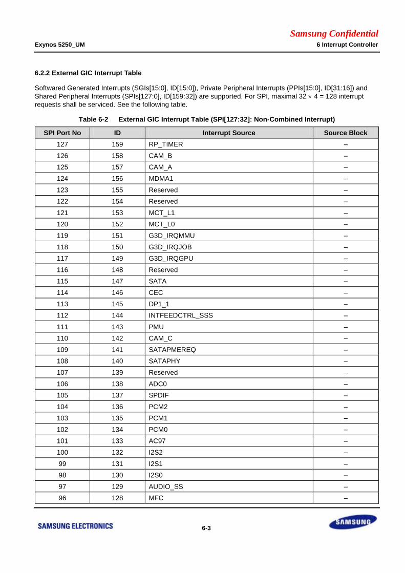
Samsung Confidential Exynos 5250_UM 6 Interrupt Controller
6-3
6.2.2 External GIC Interrupt Table
Softwared Generated Interrupts (SGIs[15:0], ID[15:0]), Private Peripheral Interrupts (PPIs[15:0], ID[31:16]) and
Shared Peripheral Interrupts (SPIs[127:0], ID[159:32]) are supported. For SPI, maximal 32 4 = 128 interrupt
requests shall be serviced. See the following table.
Table 6-2 External GIC Interrupt Table (SPI[127:32]: Non-Combined Interrupt)
SPI Port No ID Interrupt Source Source Block
127 159 RP_TIMER –
126 158 CAM_B –
125 157 CAM_A –
124 156 MDMA1 –
123 155 Reserved –
122 154 Reserved –
121 153 MCT_L1 –
120 152 MCT_L0 –
119 151 G3D_IRQMMU –
118 150 G3D_IRQJOB –
117 149 G3D_IRQGPU –
116 148 Reserved –
115 147 SATA –
114 146 CEC –
113 145 DP1_1 –
112 144 INTFEEDCTRL_SSS –
111 143 PMU –
110 142 CAM_C –
109 141 SATAPMEREQ –
108 140 SATAPHY –
107 139 Reserved –
106 138 ADC0 –
105 137 SPDIF –
104 136 PCM2 –
103 135 PCM1 –
102 134 PCM0 –
101 133 AC97 –
100 132 I2S2 –
99 131 I2S1 –
98 130 I2S0 –
97 129 AUDIO_SS –
96 128 MFC –

Samsung Confidential Exynos 5250_UM 6 Interrupt Controller
6-4
SPI Port No ID Interrupt Source Source Block
95 127 HDMI –
94 126 MIXER –
93 125 EFNFCON_1 –
92 124 EFNFCON_0 –
91 123 G2D –
90 122 EFNFCON_DMA –
89 121 JPEG –
88 120 GSCL3 –
87 119 GSCL2 –
86 118 GSCL1 –
85 117 GSCL0 –
84 116 ROTATOR –
83 115 WDT_IOP –
82 114 MIPI_DSI_4LANE –
81 113 EFNFCON_DMA_ABORT –
80 112 MIPI_CSI_B –
79 111 MIPI_CSI_A –
78 110 SDMMC3 –
77 109 SDMMC2 –
76 108 SDMMC1 –
75 107 SDMMC0 –
74 106 USBOTG –
73 105 MIPI_HSI –
72 104 USB_DRD30 –
71 103 USB_HOST20 –
70 102 SPI2 –
69 101 SPI1 –
68 100 SPI0 –
67 99 CPU_nFIQ[1] –
66 98 CPU_nFIQ[0] –
65 97 TMU –
64 96 I2C HDMI –
63 95 I2C7 –
62 94 I2C6 –
61 93 I2C5 –
60 92 I2C4 –
59 91 I2C3/USI3 –
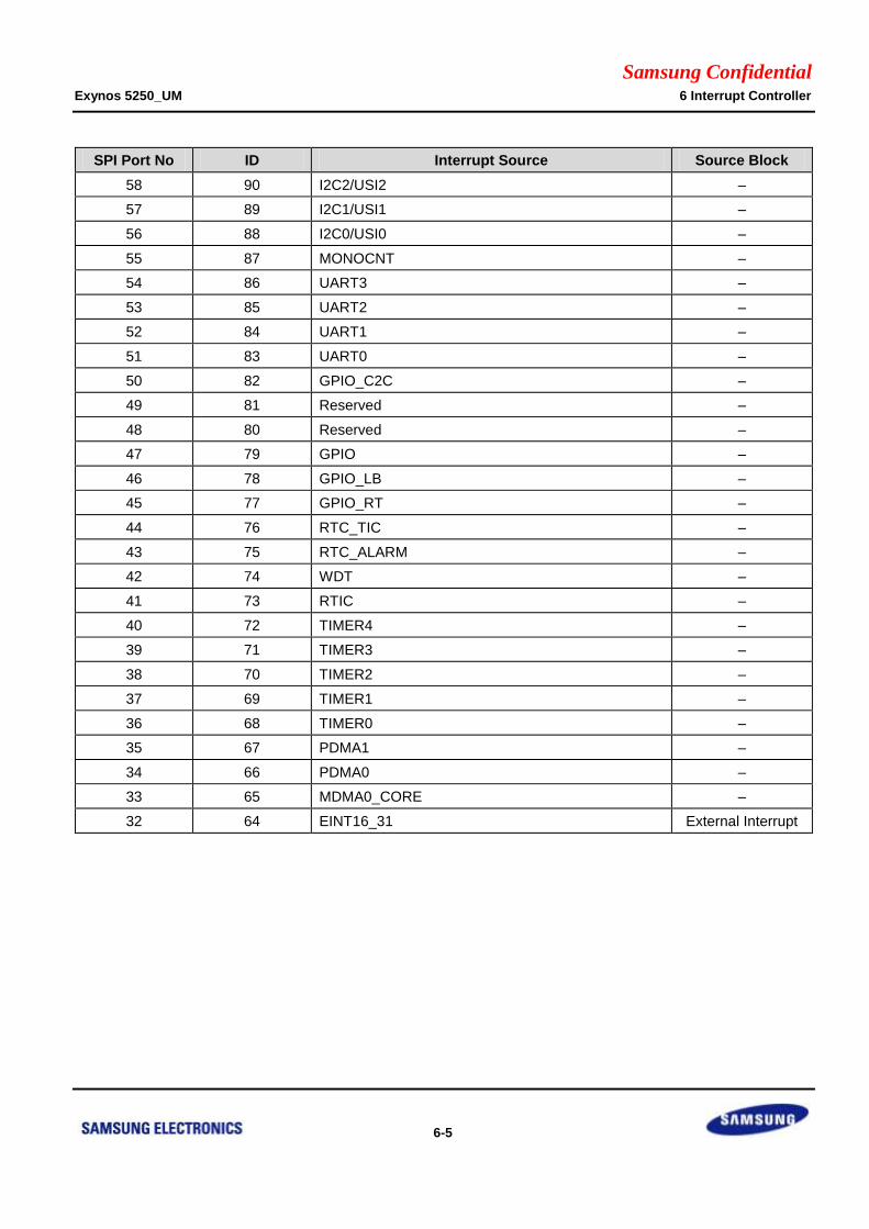
Samsung Confidential Exynos 5250_UM 6 Interrupt Controller
6-5
SPI Port No ID Interrupt Source Source Block
58 90 I2C2/USI2 –
57 89 I2C1/USI1 –
56 88 I2C0/USI0 –
55 87 MONOCNT –
54 86 UART3 –
53 85 UART2 –
52 84 UART1 –
51 83 UART0 –
50 82 GPIO_C2C –
49 81 Reserved –
48 80 Reserved –
47 79 GPIO –
46 78 GPIO_LB –
45 77 GPIO_RT –
44 76 RTC_TIC –
43 75 RTC_ALARM –
42 74 WDT –
41 73 RTIC –
40 72 TIMER4 –
39 71 TIMER3 –
38 70 TIMER2 –
37 69 TIMER1 –
36 68 TIMER0 –
35 67 PDMA1 –
34 66 PDMA0 –
33 65 MDMA0_CORE –
32 64 EINT16_31 External Interrupt
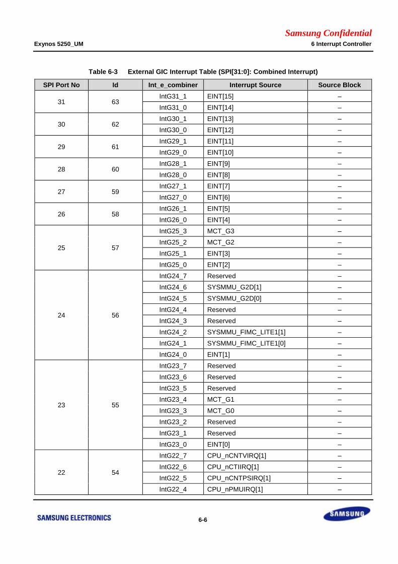
Samsung Confidential Exynos 5250_UM 6 Interrupt Controller
6-6
Table 6-3 External GIC Interrupt Table (SPI[31:0]: Combined Interrupt)
SPI Port No Id Int_e_combiner Interrupt Source Source Block
31 63 IntG31_1 EINT[15] –
IntG31_0 EINT[14] –
30 62 IntG30_1 EINT[13] –
IntG30_0 EINT[12] –
29 61 IntG29_1 EINT[11] –
IntG29_0 EINT[10] –
28 60 IntG28_1 EINT[9] –
IntG28_0 EINT[8] –
27 59 IntG27_1 EINT[7] –
IntG27_0 EINT[6] –
26 58 IntG26_1 EINT[5] –
IntG26_0 EINT[4] –
25 57
IntG25_3 MCT_G3 –
IntG25_2 MCT_G2 –
IntG25_1 EINT[3] –
IntG25_0 EINT[2] –
24 56
IntG24_7 Reserved –
IntG24_6 SYSMMU_G2D[1] –
IntG24_5 SYSMMU_G2D[0] –
IntG24_4 Reserved –
IntG24_3 Reserved –
IntG24_2 SYSMMU_FIMC_LITE1[1] –
IntG24_1 SYSMMU_FIMC_LITE1[0] –
IntG24_0 EINT[1] –
23 55
IntG23_7 Reserved –
IntG23_6 Reserved –
IntG23_5 Reserved –
IntG23_4 MCT_G1 –
IntG23_3 MCT_G0 –
IntG23_2 Reserved –
IntG23_1 Reserved –
IntG23_0 EINT[0] –
22 54
IntG22_7 CPU_nCNTVIRQ[1] –
IntG22_6 CPU_nCTIIRQ[1] –
IntG22_5 CPU_nCNTPSIRQ[1] –
IntG22_4 CPU_nPMUIRQ[1] –
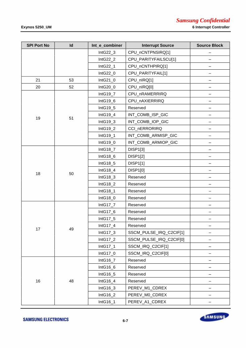
Samsung Confidential Exynos 5250_UM 6 Interrupt Controller
6-7
SPI Port No Id Int_e_combiner Interrupt Source Source Block
IntG22_3 CPU_nCNTPNSIRQ[1] –
IntG22_2 CPU_PARITYFAILSCU[1] –
IntG22_1 CPU_nCNTHPIRQ[1] –
IntG22_0 CPU_PARITYFAIL[1] –
21 53 IntG21_0 CPU_nIRQ[1] –
20 52 IntG20_0 CPU_nIRQ[0] –
19 51
IntG19_7 CPU_nRAMERRIRQ –
IntG19_6 CPU_nAXIERRIRQ –
IntG19_5 Reserved –
IntG19_4 INT_COMB_ISP_GIC –
IntG19_3 INT_COMB_IOP_GIC –
IntG19_2 CCI_nERRORIRQ –
IntG19_1 INT_COMB_ARMISP_GIC –
IntG19_0 INT_COMB_ARMIOP_GIC –
18 50
IntG18_7 DISP1[3] –
IntG18_6 DISP1[2] –
IntG18_5 DISP1[1] –
IntG18_4 DISP1[0] –
IntG18_3 Reserved –
IntG18_2 Reserved –
IntG18_1 Reserved –
IntG18_0 Reserved –
17 49
IntG17_7 Reserved –
IntG17_6 Reserved –
IntG17_5 Reserved –
IntG17_4 Reserved –
IntG17_3 SSCM_PULSE_IRQ_C2CIF[1] –
IntG17_2 SSCM_PULSE_IRQ_C2CIF[0] –
IntG17_1 SSCM_IRQ_C2CIF[1] –
IntG17_0 SSCM_IRQ_C2CIF[0] –
16 48
IntG16_7 Reserved –
IntG16_6 Reserved –
IntG16_5 Reserved –
IntG16_4 Reserved –
IntG16_3 PEREV_M1_CDREX –
IntG16_2 PEREV_M0_CDREX –
IntG16_1 PEREV_A1_CDREX –
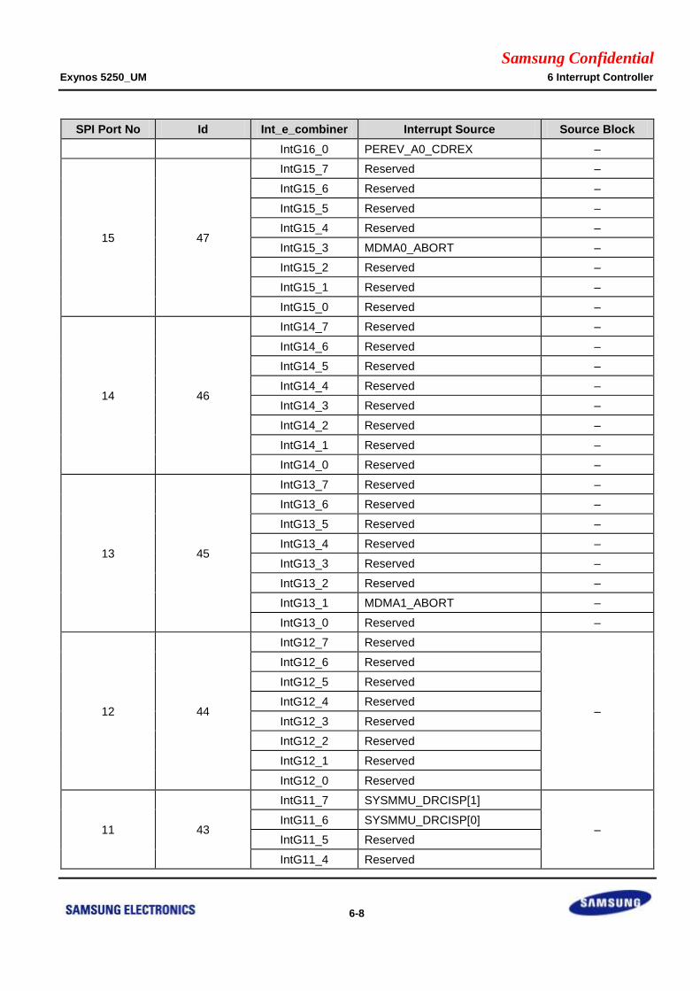
Samsung Confidential Exynos 5250_UM 6 Interrupt Controller
6-8
SPI Port No Id Int_e_combiner Interrupt Source Source Block
IntG16_0 PEREV_A0_CDREX –
15 47
IntG15_7 Reserved –
IntG15_6 Reserved –
IntG15_5 Reserved –
IntG15_4 Reserved –
IntG15_3 MDMA0_ABORT –
IntG15_2 Reserved –
IntG15_1 Reserved –
IntG15_0 Reserved –
14 46
IntG14_7 Reserved –
IntG14_6 Reserved –
IntG14_5 Reserved –
IntG14_4 Reserved –
IntG14_3 Reserved –
IntG14_2 Reserved –
IntG14_1 Reserved –
IntG14_0 Reserved –
13 45
IntG13_7 Reserved –
IntG13_6 Reserved –
IntG13_5 Reserved –
IntG13_4 Reserved –
IntG13_3 Reserved –
IntG13_2 Reserved –
IntG13_1 MDMA1_ABORT –
IntG13_0 Reserved –
12 44
IntG12_7 Reserved
–
IntG12_6 Reserved
IntG12_5 Reserved
IntG12_4 Reserved
IntG12_3 Reserved
IntG12_2 Reserved
IntG12_1 Reserved
IntG12_0 Reserved
11 43
IntG11_7 SYSMMU_DRCISP[1]
– IntG11_6 SYSMMU_DRCISP[0]
IntG11_5 Reserved
IntG11_4 Reserved
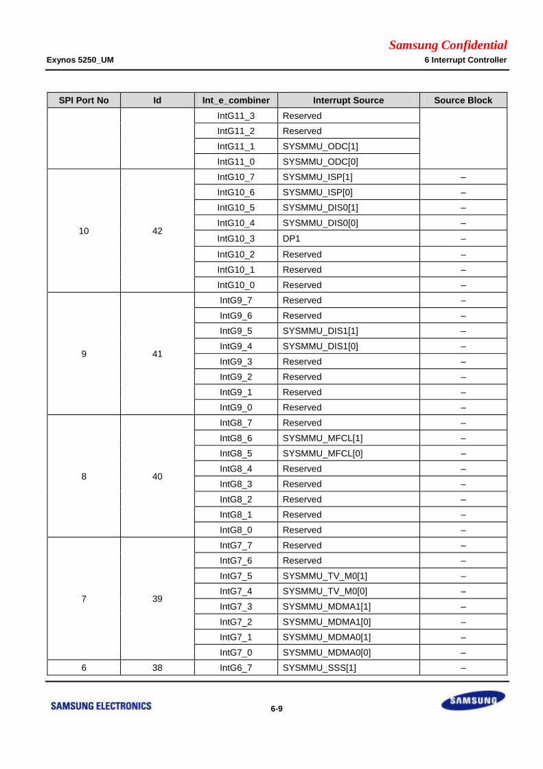
Samsung Confidential Exynos 5250_UM 6 Interrupt Controller
6-9
SPI Port No Id Int_e_combiner Interrupt Source Source Block
IntG11_3 Reserved
IntG11_2 Reserved
IntG11_1 SYSMMU_ODC[1]
IntG11_0 SYSMMU_ODC[0]
10 42
IntG10_7 SYSMMU_ISP[1] –
IntG10_6 SYSMMU_ISP[0] –
IntG10_5 SYSMMU_DIS0[1] –
IntG10_4 SYSMMU_DIS0[0] –
IntG10_3 DP1 –
IntG10_2 Reserved –
IntG10_1 Reserved –
IntG10_0 Reserved –
9 41
IntG9_7 Reserved –
IntG9_6 Reserved –
IntG9_5 SYSMMU_DIS1[1] –
IntG9_4 SYSMMU_DIS1[0] –
IntG9_3 Reserved –
IntG9_2 Reserved –
IntG9_1 Reserved –
IntG9_0 Reserved –
8 40
IntG8_7 Reserved –
IntG8_6 SYSMMU_MFCL[1] –
IntG8_5 SYSMMU_MFCL[0] –
IntG8_4 Reserved –
IntG8_3 Reserved –
IntG8_2 Reserved –
IntG8_1 Reserved –
IntG8_0 Reserved –
7 39
IntG7_7 Reserved –
IntG7_6 Reserved –
IntG7_5 SYSMMU_TV_M0[1] –
IntG7_4 SYSMMU_TV_M0[0] –
IntG7_3 SYSMMU_MDMA1[1] –
IntG7_2 SYSMMU_MDMA1[0] –
IntG7_1 SYSMMU_MDMA0[1] –
IntG7_0 SYSMMU_MDMA0[0] –
6 38 IntG6_7 SYSMMU_SSS[1] –
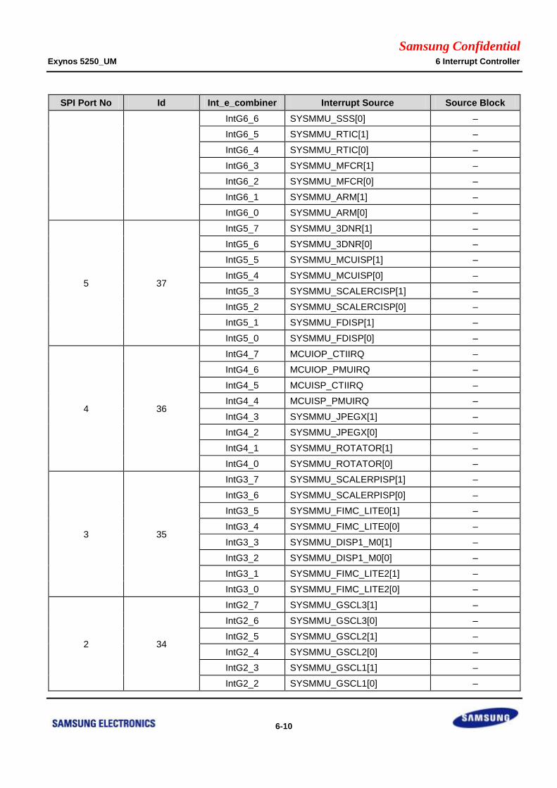
Samsung Confidential Exynos 5250_UM 6 Interrupt Controller
6-10
SPI Port No Id Int_e_combiner Interrupt Source Source Block
IntG6_6 SYSMMU_SSS[0] –
IntG6_5 SYSMMU_RTIC[1] –
IntG6_4 SYSMMU_RTIC[0] –
IntG6_3 SYSMMU_MFCR[1] –
IntG6_2 SYSMMU_MFCR[0] –
IntG6_1 SYSMMU_ARM[1] –
IntG6_0 SYSMMU_ARM[0] –
5 37
IntG5_7 SYSMMU_3DNR[1] –
IntG5_6 SYSMMU_3DNR[0] –
IntG5_5 SYSMMU_MCUISP[1] –
IntG5_4 SYSMMU_MCUISP[0] –
IntG5_3 SYSMMU_SCALERCISP[1] –
IntG5_2 SYSMMU_SCALERCISP[0] –
IntG5_1 SYSMMU_FDISP[1] –
IntG5_0 SYSMMU_FDISP[0] –
4 36
IntG4_7 MCUIOP_CTIIRQ –
IntG4_6 MCUIOP_PMUIRQ –
IntG4_5 MCUISP_CTIIRQ –
IntG4_4 MCUISP_PMUIRQ –
IntG4_3 SYSMMU_JPEGX[1] –
IntG4_2 SYSMMU_JPEGX[0] –
IntG4_1 SYSMMU_ROTATOR[1] –
IntG4_0 SYSMMU_ROTATOR[0] –
3 35
IntG3_7 SYSMMU_SCALERPISP[1] –
IntG3_6 SYSMMU_SCALERPISP[0] –
IntG3_5 SYSMMU_FIMC_LITE0[1] –
IntG3_4 SYSMMU_FIMC_LITE0[0] –
IntG3_3 SYSMMU_DISP1_M0[1] –
IntG3_2 SYSMMU_DISP1_M0[0] –
IntG3_1 SYSMMU_FIMC_LITE2[1] –
IntG3_0 SYSMMU_FIMC_LITE2[0] –
2 34
IntG2_7 SYSMMU_GSCL3[1] –
IntG2_6 SYSMMU_GSCL3[0] –
IntG2_5 SYSMMU_GSCL2[1] –
IntG2_4 SYSMMU_GSCL2[0] –
IntG2_3 SYSMMU_GSCL1[1] –
IntG2_2 SYSMMU_GSCL1[0] –
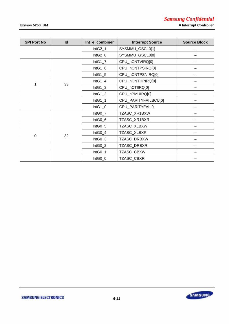
Samsung Confidential Exynos 5250_UM 6 Interrupt Controller
6-11
SPI Port No Id Int_e_combiner Interrupt Source Source Block
IntG2_1 SYSMMU_GSCL0[1] –
IntG2_0 SYSMMU_GSCL0[0] –
1 33
IntG1_7 CPU_nCNTVIRQ[0] –
IntG1_6 CPU_nCNTPSIRQ[0] –
IntG1_5 CPU_nCNTPSNIRQ[0] –
IntG1_4 CPU_nCNTHPIRQ[0] –
IntG1_3 CPU_nCTIIRQ[0] –
IntG1_2 CPU_nPMUIRQ[0] –
IntG1_1 CPU_PARITYFAILSCU[0] –
IntG1_0 CPU_PARITYFAIL0 –
0 32
IntG0_7 TZASC_XR1BXW –
IntG0_6 TZASC_XR1BXR –
IntG0_5 TZASC_XLBXW –
IntG0_4 TZASC_XLBXR –
IntG0_3 TZASC_DRBXW –
IntG0_2 TZASC_DRBXR –
IntG0_1 TZASC_CBXW –
IntG0_0 TZASC_CBXR –
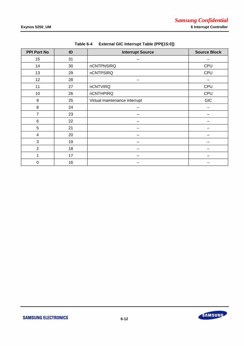
Samsung Confidential Exynos 5250_UM 6 Interrupt Controller
6-12
Table 6-4 External GIC Interrupt Table (PPI[15:0])
PPI Port No ID Interrupt Source Source Block
15 31 – –
14 30 nCNTPNSIRQ CPU
13 29 nCNTPSIRQ CPU
12 28 – –
11 27 nCNTVIRQ CPU
10 26 nCNTHPIRQ CPU
9 25 Virtual maintenance interrupt GIC
8 24 – –
7 23 – –
6 22 – –
5 21 – –
4 20 – –
3 19 – –
2 18 – –
1 17 – –
0 16 – –
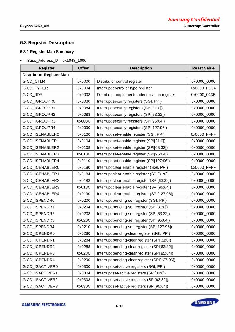
Samsung Confidential Exynos 5250_UM 6 Interrupt Controller
6-13
6.3 Register Description
6.3.1 Register Map Summary
Base_Address_D = 0x1048_1000
Register Offset Description Reset Value
Distributor Register Map
GICD_CTLR 0x0000 Distributor control register 0x0000_0000
GICD_TYPER 0x0004 Interrupt controller type register 0x0000_FC24
GICD_IIDR 0x0008 Distributor implementer identification register 0x0200_043B
GICD_IGROUPR0 0x0080 Interrupt security registers (SGI, PPI) 0x0000_0000
GICD_IGROUPR1 0x0084 Interrupt security registers (SPI[31:0]) 0x0000_0000
GICD_IGROUPR2 0x0088 Interrupt security registers (SPI[63:32]) 0x0000_0000
GICD_IGROUPR3 0x008C Interrupt security registers (SPI[95:64]) 0x0000_0000
GICD_IGROUPR4 0x0090 Interrupt security registers (SPI[127:96]) 0x0000_0000
GICD_ISENABLER0 0x0100 Interrupt set-enable register (SGI, PPI) 0x0000_FFFF
GICD_ISENABLER1 0x0104 Interrupt set-enable register (SPI[31:0]) 0x0000_0000
GICD_ISENABLER2 0x0108 Interrupt set-enable register (SPI[63:32]) 0x0000_0000
GICD_ISENABLER3 0x010C Interrupt set-enable register (SPI[95:64]) 0x0000_0000
GICD_ISENABLER4 0x0110 Interrupt set-enable register (SPI[127:96]) 0x0000_0000
GICD_ICENABLER0 0x0180 Interrupt clear-enable register (SGI, PPI) 0x0000_FFFF
GICD_ICENABLER1 0x0184 Interrupt clear-enable register (SPI[31:0]) 0x0000_0000
GICD_ICENABLER2 0x0188 Interrupt clear-enable register (SPI[63:32]) 0x0000_0000
GICD_ICENABLER3 0x018C Interrupt clear-enable register (SPI[95:64]) 0x0000_0000
GICD_ICENABLER4 0x0190 Interrupt clear-enable register (SPI[127:96]) 0x0000_0000
GICD_ISPENDR0 0x0200 Interrupt pending-set register (SGI, PPI) 0x0000_0000
GICD_ISPENDR1 0x0204 Interrupt pending-set register (SPI[31:0]) 0x0000_0000
GICD_ISPENDR2 0x0208 Interrupt pending-set register (SPI[63:32]) 0x0000_0000
GICD_ISPENDR3 0x020C Interrupt pending-set register (SPI[95:64]) 0x0000_0000
GICD_ISPENDR4 0x0210 Interrupt pending-set register (SPI[127:96]) 0x0000_0000
GICD_ICPENDR0 0x0280 Interrupt pending-clear register (SGI, PPI) 0x0000_0000
GICD_ICPENDR1 0x0284 Interrupt pending-clear register (SPI[31:0]) 0x0000_0000
GICD_ICPENDR2 0x0288 Interrupt pending-clear register (SPI[63:32]) 0x0000_0000
GICD_ICPENDR3 0x028C Interrupt pending-clear register (SPI[95:64]) 0x0000_0000
GICD_ICPENDR4 0x0290 Interrupt pending-clear register (SPI[127:96]) 0x0000_0000
GICD_ISACTIVER0 0x0300 Interrupt set-active registers (SGI, PPI) 0x0000_0000
GICD_ISACTIVER1 0x0304 Interrupt set-active registers (SPI[31:0]) 0x0000_0000
GICD_ISACTIVER2 0x0308 Interrupt set-active registers (SPI[63:32]) 0x0000_0000
GICD_ISACTIVER3 0x030C Interrupt set-active registers (SPI[95:64]) 0x0000_0000
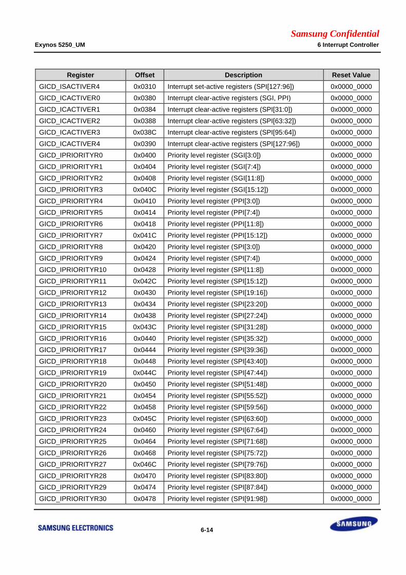
Samsung Confidential Exynos 5250_UM 6 Interrupt Controller
6-14
Register Offset Description Reset Value
GICD_ISACTIVER4 0x0310 Interrupt set-active registers (SPI[127:96]) 0x0000_0000
GICD_ICACTIVER0 0x0380 Interrupt clear-active registers (SGI, PPI) 0x0000_0000
GICD_ICACTIVER1 0x0384 Interrupt clear-active registers (SPI[31:0]) 0x0000_0000
GICD_ICACTIVER2 0x0388 Interrupt clear-active registers (SPI[63:32]) 0x0000_0000
GICD_ICACTIVER3 0x038C Interrupt clear-active registers (SPI[95:64]) 0x0000_0000
GICD_ICACTIVER4 0x0390 Interrupt clear-active registers (SPI[127:96]) 0x0000_0000
GICD_IPRIORITYR0 0x0400 Priority level register (SGI[3:0]) 0x0000_0000
GICD_IPRIORITYR1 0x0404 Priority level register (SGI[7:4]) 0x0000_0000
GICD_IPRIORITYR2 0x0408 Priority level register (SGI[11:8]) 0x0000_0000
GICD_IPRIORITYR3 0x040C Priority level register (SGI[15:12]) 0x0000_0000
GICD_IPRIORITYR4 0x0410 Priority level register (PPI[3:0]) 0x0000_0000
GICD_IPRIORITYR5 0x0414 Priority level register (PPI[7:4]) 0x0000_0000
GICD_IPRIORITYR6 0x0418 Priority level register (PPI[11:8]) 0x0000_0000
GICD_IPRIORITYR7 0x041C Priority level register (PPI[15:12]) 0x0000_0000
GICD_IPRIORITYR8 0x0420 Priority level register (SPI[3:0]) 0x0000_0000
GICD_IPRIORITYR9 0x0424 Priority level register (SPI[7:4]) 0x0000_0000
GICD_IPRIORITYR10 0x0428 Priority level register (SPI[11:8]) 0x0000_0000
GICD_IPRIORITYR11 0x042C Priority level register (SPI[15:12]) 0x0000_0000
GICD_IPRIORITYR12 0x0430 Priority level register (SPI[19:16]) 0x0000_0000
GICD_IPRIORITYR13 0x0434 Priority level register (SPI[23:20]) 0x0000_0000
GICD_IPRIORITYR14 0x0438 Priority level register (SPI[27:24]) 0x0000_0000
GICD_IPRIORITYR15 0x043C Priority level register (SPI[31:28]) 0x0000_0000
GICD_IPRIORITYR16 0x0440 Priority level register (SPI[35:32]) 0x0000_0000
GICD_IPRIORITYR17 0x0444 Priority level register (SPI[39:36]) 0x0000_0000
GICD_IPRIORITYR18 0x0448 Priority level register (SPI[43:40]) 0x0000_0000
GICD_IPRIORITYR19 0x044C Priority level register (SPI[47:44]) 0x0000_0000
GICD_IPRIORITYR20 0x0450 Priority level register (SPI[51:48]) 0x0000_0000
GICD_IPRIORITYR21 0x0454 Priority level register (SPI[55:52]) 0x0000_0000
GICD_IPRIORITYR22 0x0458 Priority level register (SPI[59:56]) 0x0000_0000
GICD_IPRIORITYR23 0x045C Priority level register (SPI[63:60]) 0x0000_0000
GICD_IPRIORITYR24 0x0460 Priority level register (SPI[67:64]) 0x0000_0000
GICD_IPRIORITYR25 0x0464 Priority level register (SPI[71:68]) 0x0000_0000
GICD_IPRIORITYR26 0x0468 Priority level register (SPI[75:72]) 0x0000_0000
GICD_IPRIORITYR27 0x046C Priority level register (SPI[79:76]) 0x0000_0000
GICD_IPRIORITYR28 0x0470 Priority level register (SPI[83:80]) 0x0000_0000
GICD_IPRIORITYR29 0x0474 Priority level register (SPI[87:84]) 0x0000_0000
GICD_IPRIORITYR30 0x0478 Priority level register (SPI[91:98]) 0x0000_0000
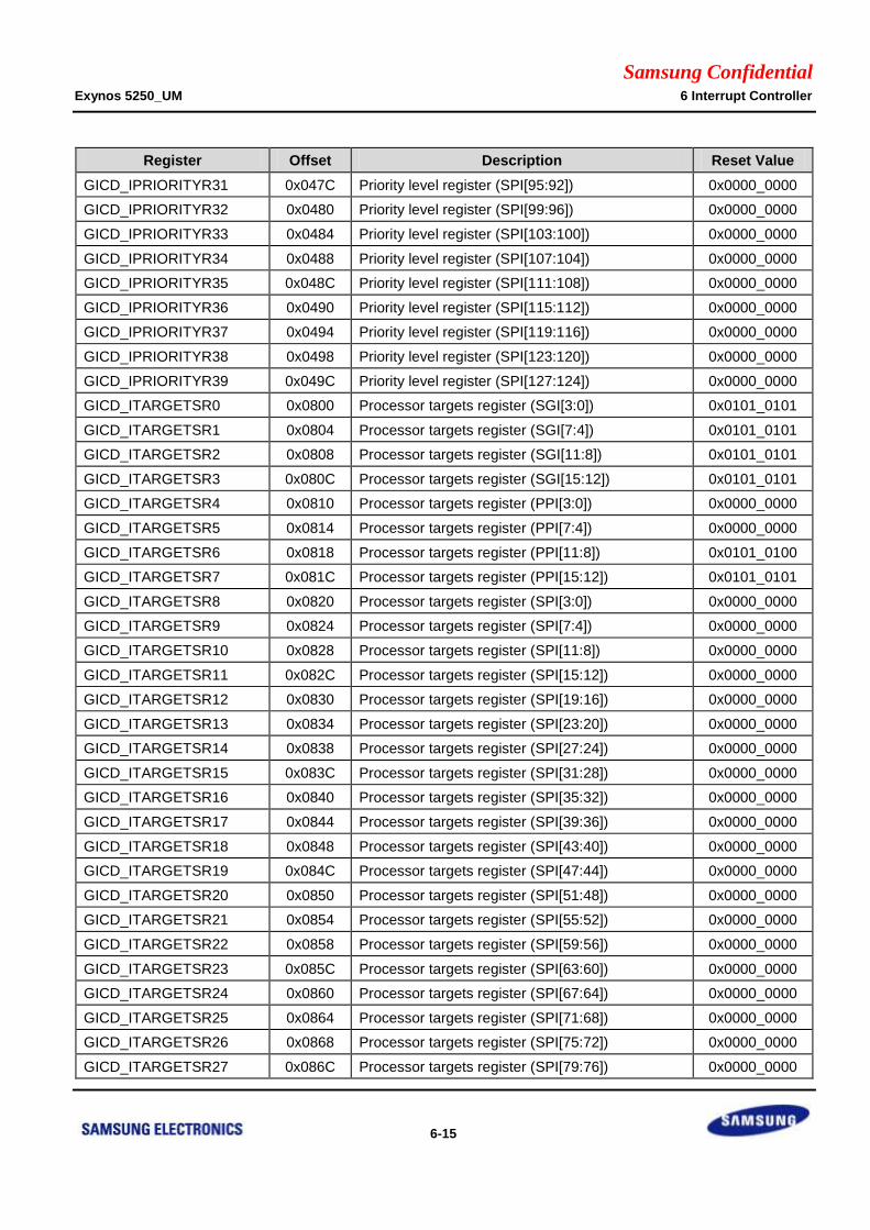
Samsung Confidential Exynos 5250_UM 6 Interrupt Controller
6-15
Register Offset Description Reset Value
GICD_IPRIORITYR31 0x047C Priority level register (SPI[95:92]) 0x0000_0000
GICD_IPRIORITYR32 0x0480 Priority level register (SPI[99:96]) 0x0000_0000
GICD_IPRIORITYR33 0x0484 Priority level register (SPI[103:100]) 0x0000_0000
GICD_IPRIORITYR34 0x0488 Priority level register (SPI[107:104]) 0x0000_0000
GICD_IPRIORITYR35 0x048C Priority level register (SPI[111:108]) 0x0000_0000
GICD_IPRIORITYR36 0x0490 Priority level register (SPI[115:112]) 0x0000_0000
GICD_IPRIORITYR37 0x0494 Priority level register (SPI[119:116]) 0x0000_0000
GICD_IPRIORITYR38 0x0498 Priority level register (SPI[123:120]) 0x0000_0000
GICD_IPRIORITYR39 0x049C Priority level register (SPI[127:124]) 0x0000_0000
GICD_ITARGETSR0 0x0800 Processor targets register (SGI[3:0]) 0x0101_0101
GICD_ITARGETSR1 0x0804 Processor targets register (SGI[7:4]) 0x0101_0101
GICD_ITARGETSR2 0x0808 Processor targets register (SGI[11:8]) 0x0101_0101
GICD_ITARGETSR3 0x080C Processor targets register (SGI[15:12]) 0x0101_0101
GICD_ITARGETSR4 0x0810 Processor targets register (PPI[3:0]) 0x0000_0000
GICD_ITARGETSR5 0x0814 Processor targets register (PPI[7:4]) 0x0000_0000
GICD_ITARGETSR6 0x0818 Processor targets register (PPI[11:8]) 0x0101_0100
GICD_ITARGETSR7 0x081C Processor targets register (PPI[15:12]) 0x0101_0101
GICD_ITARGETSR8 0x0820 Processor targets register (SPI[3:0]) 0x0000_0000
GICD_ITARGETSR9 0x0824 Processor targets register (SPI[7:4]) 0x0000_0000
GICD_ITARGETSR10 0x0828 Processor targets register (SPI[11:8]) 0x0000_0000
GICD_ITARGETSR11 0x082C Processor targets register (SPI[15:12]) 0x0000_0000
GICD_ITARGETSR12 0x0830 Processor targets register (SPI[19:16]) 0x0000_0000
GICD_ITARGETSR13 0x0834 Processor targets register (SPI[23:20]) 0x0000_0000
GICD_ITARGETSR14 0x0838 Processor targets register (SPI[27:24]) 0x0000_0000
GICD_ITARGETSR15 0x083C Processor targets register (SPI[31:28]) 0x0000_0000
GICD_ITARGETSR16 0x0840 Processor targets register (SPI[35:32]) 0x0000_0000
GICD_ITARGETSR17 0x0844 Processor targets register (SPI[39:36]) 0x0000_0000
GICD_ITARGETSR18 0x0848 Processor targets register (SPI[43:40]) 0x0000_0000
GICD_ITARGETSR19 0x084C Processor targets register (SPI[47:44]) 0x0000_0000
GICD_ITARGETSR20 0x0850 Processor targets register (SPI[51:48]) 0x0000_0000
GICD_ITARGETSR21 0x0854 Processor targets register (SPI[55:52]) 0x0000_0000
GICD_ITARGETSR22 0x0858 Processor targets register (SPI[59:56]) 0x0000_0000
GICD_ITARGETSR23 0x085C Processor targets register (SPI[63:60]) 0x0000_0000
GICD_ITARGETSR24 0x0860 Processor targets register (SPI[67:64]) 0x0000_0000
GICD_ITARGETSR25 0x0864 Processor targets register (SPI[71:68]) 0x0000_0000
GICD_ITARGETSR26 0x0868 Processor targets register (SPI[75:72]) 0x0000_0000
GICD_ITARGETSR27 0x086C Processor targets register (SPI[79:76]) 0x0000_0000
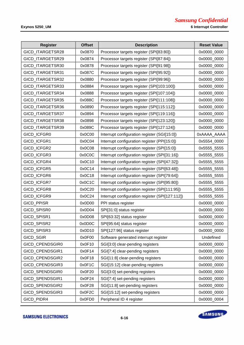
Samsung Confidential Exynos 5250_UM 6 Interrupt Controller
6-16
Register Offset Description Reset Value
GICD_ITARGETSR28 0x0870 Processor targets register (SPI[83:80]) 0x0000_0000
GICD_ITARGETSR29 0x0874 Processor targets register (SPI[87:84]) 0x0000_0000
GICD_ITARGETSR30 0x0878 Processor targets register (SPI[91:98]) 0x0000_0000
GICD_ITARGETSR31 0x087C Processor targets register (SPI[95:92]) 0x0000_0000
GICD_ITARGETSR32 0x0880 Processor targets register (SPI[99:96]) 0x0000_0000
GICD_ITARGETSR33 0x0884 Processor targets register (SPI[103:100]) 0x0000_0000
GICD_ITARGETSR34 0x0888 Processor targets register (SPI[107:104]) 0x0000_0000
GICD_ITARGETSR35 0x088C Processor targets register (SPI[111:108]) 0x0000_0000
GICD_ITARGETSR36 0x0890 Processor targets register (SPI[115:112]) 0x0000_0000
GICD_ITARGETSR37 0x0894 Processor targets register (SPI[119:116]) 0x0000_0000
GICD_ITARGETSR38 0x0898 Processor targets register (SPI[123:120]) 0x0000_0000
GICD_ITARGETSR39 0x089C Processor targets register (SPI[127:124]) 0x0000_0000
GICD_ICFGR0 0x0C00 Interrupt configuration register (SGI[15:0]) 0xAAAA_AAAA
GICD_ICFGR1 0x0C04 Interrupt configuration register (PPI[15:0]) 0x5554_0000
GICD_ICFGR2 0x0C08 Interrupt configuration register (SPI[15:0]) 0x5555_5555
GICD_ICFGR3 0x0C0C Interrupt configuration register (SPI[31:16]) 0x5555_5555
GICD_ICFGR4 0x0C10 Interrupt configuration register (SPI[47:32]) 0x5555_5555
GICD_ICFGR5 0x0C14 Interrupt configuration register (SPI[63:48]) 0x5555_5555
GICD_ICFGR6 0x0C18 Interrupt configuration register (SPI[79:64]) 0x5555_5555
GICD_ICFGR7 0x0C1C Interrupt configuration register (SPI[95:80]) 0x5555_5555
GICD_ICFGR8 0x0C20 Interrupt configuration register (SPI[111:95]) 0x5555_5555
GICD_ICFGR9 0x0C24 Interrupt configuration register (SPI[127:112]) 0x5555_5555
GICD_PPISR 0x0D00 PPI status register 0x0000_0000
GICD_SPISR0 0x0D04 SPI[31:0] status register 0x0000_0000
GICD_SPISR1 0x0D08 SPI[63:32] status register 0x0000_0000
GICD_SPISR2 0x0D0C SPI[95:64] status register 0x0000_0000
GICD_SPISR3 0x0D10 SPI[127:96] status register 0x0000_0000
GICD_SGIR 0x0F00 Software generated interrupt register Undefined
GICD_CPENDSGIR0 0x0F10 SGI[3:0] clear-pending registers 0x0000_0000
GICD_CPENDSGIR1 0x0F14 SGI[7:4] clear-pending registers 0x0000_0000
GICD_CPENDSGIR2 0x0F18 SGI[11:8] clear-pending registers 0x0000_0000
GICD_CPENDSGIR3 0x0F1C SGI[15:12] clear-pending registers 0x0000_0000
GICD_SPENDSGIR0 0x0F20 SGI[3:0] set-pending registers 0x0000_0000
GICD_SPENDSGIR1 0x0F24 SGI[7:4] set-pending registers 0x0000_0000
GICD_SPENDSGIR2 0x0F28 SGI[11:8] set-pending registers 0x0000_0000
GICD_SPENDSGIR3 0x0F2C SGI[15:12] set-pending registers 0x0000_0000
GICD_PIDR4 0x0FD0 Peripheral ID 4 register 0x0000_0004
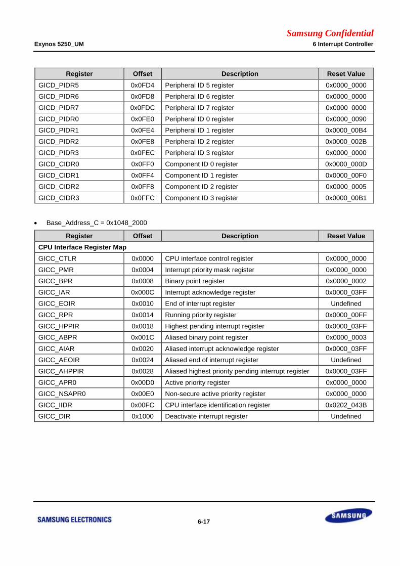
Samsung Confidential Exynos 5250_UM 6 Interrupt Controller
6-17
Register Offset Description Reset Value
GICD_PIDR5 0x0FD4 Peripheral ID 5 register 0x0000_0000
GICD_PIDR6 0x0FD8 Peripheral ID 6 register 0x0000_0000
GICD_PIDR7 0x0FDC Peripheral ID 7 register 0x0000_0000
GICD_PIDR0 0x0FE0 Peripheral ID 0 register 0x0000_0090
GICD_PIDR1 0x0FE4 Peripheral ID 1 register 0x0000_00B4
GICD_PIDR2 0x0FE8 Peripheral ID 2 register 0x0000_002B
GICD_PIDR3 0x0FEC Peripheral ID 3 register 0x0000_0000
GICD_CIDR0 0x0FF0 Component ID 0 register 0x0000_000D
GICD_CIDR1 0x0FF4 Component ID 1 register 0x0000_00F0
GICD_CIDR2 0x0FF8 Component ID 2 register 0x0000_0005
GICD_CIDR3 0x0FFC Component ID 3 register 0x0000_00B1
Base_Address_C = 0x1048_2000
Register Offset Description Reset Value
CPU Interface Register Map
GICC_CTLR 0x0000 CPU interface control register 0x0000_0000
GICC_PMR 0x0004 Interrupt priority mask register 0x0000_0000
GICC_BPR 0x0008 Binary point register 0x0000_0002
GICC_IAR 0x000C Interrupt acknowledge register 0x0000_03FF
GICC_EOIR 0x0010 End of interrupt register Undefined
GICC_RPR 0x0014 Running priority register 0x0000_00FF
GICC_HPPIR 0x0018 Highest pending interrupt register 0x0000_03FF
GICC_ABPR 0x001C Aliased binary point register 0x0000_0003
GICC_AIAR 0x0020 Aliased interrupt acknowledge register 0x0000_03FF
GICC_AEOIR 0x0024 Aliased end of interrupt register Undefined
GICC_AHPPIR 0x0028 Aliased highest priority pending interrupt register 0x0000_03FF
GICC_APR0 0x00D0 Active priority register 0x0000_0000
GICC_NSAPR0 0x00E0 Non-secure active priority register 0x0000_0000
GICC_IIDR 0x00FC CPU interface identification register 0x0202_043B
GICC_DIR 0x1000 Deactivate interrupt register Undefined
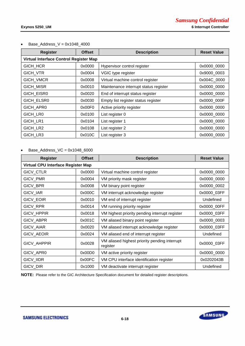
Samsung Confidential Exynos 5250_UM 6 Interrupt Controller
6-18
Base_Address_V = 0x1048_4000
Register Offset Description Reset Value
Virtual Interface Control Register Map
GICH_HCR 0x0000 Hypervisor control register 0x0000_0000
GICH_VTR 0x0004 VGIC type register 0x9000_0003
GICH_VMCR 0x0008 Virtual machine control register 0x004C_0000
GICH_MISR 0x0010 Maintenance interrupt status register 0x0000_0000
GICH_EISR0 0x0020 End of interrupt status register 0x0000_0000
GICH_ELSR0 0x0030 Empty list register status register 0x0000_000F
GICH_APR0 0x00F0 Active priority register 0x0000_0000
GICH_LR0 0x0100 List register 0 0x0000_0000
GICH_LR1 0x0104 List register 1 0x0000_0000
GICH_LR2 0x0108 List register 2 0x0000_0000
GICH_LR3 0x010C List register 3 0x0000_0000
Base_Address_VC = 0x1048_6000
Register Offset Description Reset Value
Virtual CPU Interface Register Map
GICV_CTLR 0x0000 Virtual machine control register 0x0000_0000
GICV_PMR 0x0004 VM priority mask register 0x0000_0000
GICV_BPR 0x0008 VM binary point register 0x0000_0002
GICV_IAR 0x000C VM interrupt acknowledge register 0x0000_03FF
GICV_EOIR 0x0010 VM end of interrupt register Undefined
GICV_RPR 0x0014 VM running priority register 0x0000_00FF
GICV_HPPIR 0x0018 VM highest priority pending interrupt register 0x0000_03FF
GICV_ABPR 0x001C VM aliased binary point register 0x0000_0003
GICV_AIAR 0x0020 VM aliased interrupt acknowledge register 0x0000_03FF
GICV_AEOIR 0x0024 VM aliased end of interrupt register Undefined
GICV_AHPPIR 0x0028 VM aliased highest priority pending interrupt
register 0x0000_03FF
GICV_APR0 0x00D0 VM active priority register 0x0000_0000
GICV_IIDR 0x00FC VM CPU interface identification register 0x0202043B
GICV_DIR 0x1000 VM deactivate interrupt register Undefined
NOTE: Please refer to the GIC Architecture Specification document for detailed register descriptions.
Samsung Confidential Exynos 5250_UM 7 Interrupt Combiner
7-1
7 Interrupt Combiner
7.1 Overview
The interrupt controller subsystem in Exynos 5250 consists of generic interrupt controllers and interrupt
combiners. Some interrupt sources are grouped in Exynos 5250. The interrupt combiner combines several
interrupt sources as a group. Several interrupt requests in a group, create a group interrupt request, which
produces a single request signal. Therefore, the interrupt input sources of the generic interrupt controller consists
of the group interrupt requests from the interrupt combiner and uncombined interrupt sources.
7.2 Features
The features for interrupt combiner are:
Supports 32 group interrupt outputs for the interrupt combiner
Provides Enable/Mask of each interrupt source in a group
Provides Status of each interrupt source in a group before interrupt masking
Provides Status of each interrupt source in a group after interrupt masking
Provides Status of each group interrupt output after interrupt masking and combining
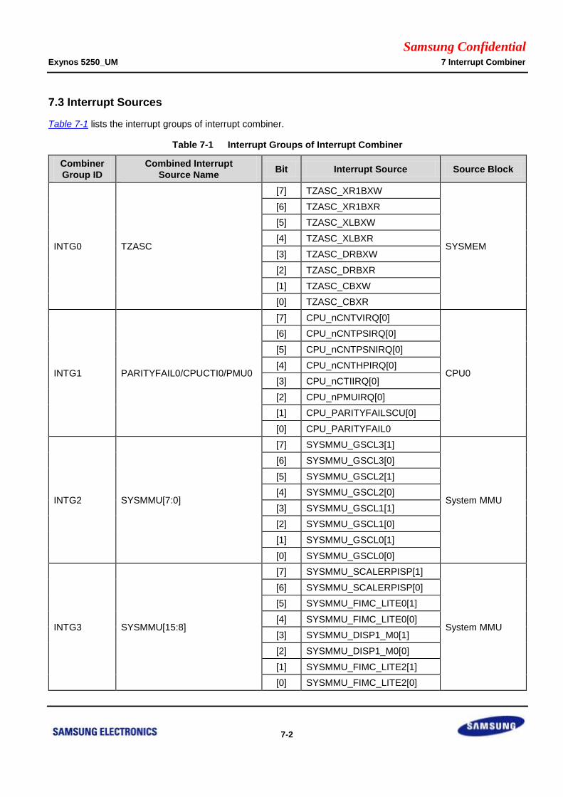
Samsung Confidential Exynos 5250_UM 7 Interrupt Combiner
7-2
7.3 Interrupt Sources
Table 7-1 lists the interrupt groups of interrupt combiner.
Table 7-1 Interrupt Groups of Interrupt Combiner
Combiner
Group ID
Combined Interrupt
Source Name Bit Interrupt Source Source Block
INTG0 TZASC
[7] TZASC_XR1BXW
SYSMEM
[6] TZASC_XR1BXR
[5] TZASC_XLBXW
[4] TZASC_XLBXR
[3] TZASC_DRBXW
[2] TZASC_DRBXR
[1] TZASC_CBXW
[0] TZASC_CBXR
INTG1 PARITYFAIL0/CPUCTI0/PMU0
[7] CPU_nCNTVIRQ[0]
CPU0
[6] CPU_nCNTPSIRQ[0]
[5] CPU_nCNTPSNIRQ[0]
[4] CPU_nCNTHPIRQ[0]
[3] CPU_nCTIIRQ[0]
[2] CPU_nPMUIRQ[0]
[1] CPU_PARITYFAILSCU[0]
[0] CPU_PARITYFAIL0
INTG2 SYSMMU[7:0]
[7] SYSMMU_GSCL3[1]
System MMU
[6] SYSMMU_GSCL3[0]
[5] SYSMMU_GSCL2[1]
[4] SYSMMU_GSCL2[0]
[3] SYSMMU_GSCL1[1]
[2] SYSMMU_GSCL1[0]
[1] SYSMMU_GSCL0[1]
[0] SYSMMU_GSCL0[0]
INTG3 SYSMMU[15:8]
[7] SYSMMU_SCALERPISP[1]
System MMU
[6] SYSMMU_SCALERPISP[0]
[5] SYSMMU_FIMC_LITE0[1]
[4] SYSMMU_FIMC_LITE0[0]
[3] SYSMMU_DISP1_M0[1]
[2] SYSMMU_DISP1_M0[0]
[1] SYSMMU_FIMC_LITE2[1]
[0] SYSMMU_FIMC_LITE2[0]
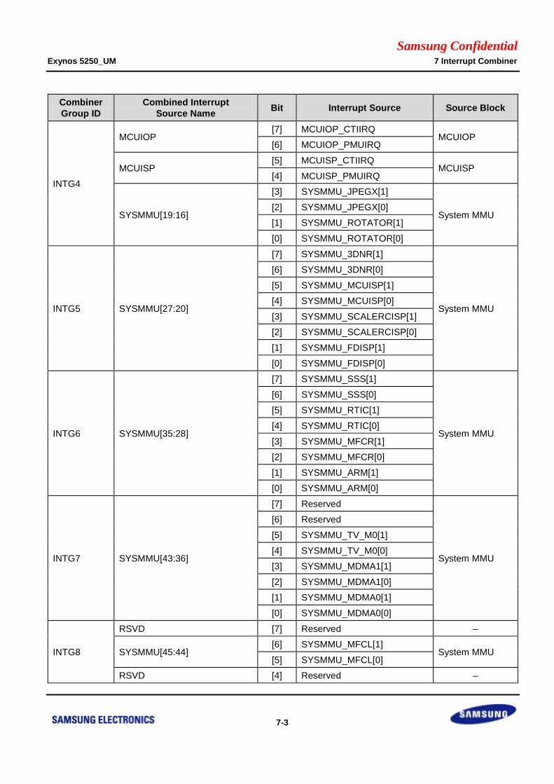
Samsung Confidential Exynos 5250_UM 7 Interrupt Combiner
7-3
Combiner
Group ID
Combined Interrupt
Source Name Bit Interrupt Source Source Block
INTG4
MCUIOP [7] MCUIOP_CTIIRQ
MCUIOP [6] MCUIOP_PMUIRQ
MCUISP [5] MCUISP_CTIIRQ
MCUISP [4] MCUISP_PMUIRQ
SYSMMU[19:16]
[3] SYSMMU_JPEGX[1]
System MMU [2] SYSMMU_JPEGX[0]
[1] SYSMMU_ROTATOR[1]
[0] SYSMMU_ROTATOR[0]
INTG5 SYSMMU[27:20]
[7] SYSMMU_3DNR[1]
System MMU
[6] SYSMMU_3DNR[0]
[5] SYSMMU_MCUISP[1]
[4] SYSMMU_MCUISP[0]
[3] SYSMMU_SCALERCISP[1]
[2] SYSMMU_SCALERCISP[0]
[1] SYSMMU_FDISP[1]
[0] SYSMMU_FDISP[0]
INTG6 SYSMMU[35:28]
[7] SYSMMU_SSS[1]
System MMU
[6] SYSMMU_SSS[0]
[5] SYSMMU_RTIC[1]
[4] SYSMMU_RTIC[0]
[3] SYSMMU_MFCR[1]
[2] SYSMMU_MFCR[0]
[1] SYSMMU_ARM[1]
[0] SYSMMU_ARM[0]
INTG7 SYSMMU[43:36]
[7] Reserved
System MMU
[6] Reserved
[5] SYSMMU_TV_M0[1]
[4] SYSMMU_TV_M0[0]
[3] SYSMMU_MDMA1[1]
[2] SYSMMU_MDMA1[0]
[1] SYSMMU_MDMA0[1]
[0] SYSMMU_MDMA0[0]
INTG8
RSVD [7] Reserved –
SYSMMU[45:44] [6] SYSMMU_MFCL[1]
System MMU [5] SYSMMU_MFCL[0]
RSVD [4] Reserved –
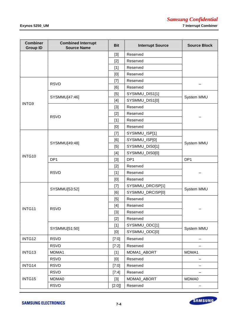
Samsung Confidential Exynos 5250_UM 7 Interrupt Combiner
7-4
Combiner
Group ID
Combined Interrupt
Source Name Bit Interrupt Source Source Block
[3] Reserved
[2] Reserved
[1] Reserved
[0] Reserved
INTG9
RSVD [7] Reserved
– [6] Reserved
SYSMMU[47:46] [5] SYSMMU_DIS1[1]
System MMU [4] SYSMMU_DIS1[0]
RSVD
[3] Reserved
– [2] Reserved
[1] Reserved
[0] Reserved
INTG10
SYSMMU[49:48]
[7] SYSMMU_ISP[1]
System MMU [6] SYSMMU_ISP[0]
[5] SYSMMU_DIS0[1]
[4] SYSMMU_DIS0[0]
DP1 [3] DP1 DP1
RSVD
[2] Reserved
– [1] Reserved
[0] Reserved
INTG11
SYSMMU[53:52] [7] SYSMMU_DRCISP[1]
System MMU [6] SYSMMU_DRCISP[0]
RSVD
[5] Reserved
– [4] Reserved
[3] Reserved
[2] Reserved
SYSMMU[51:50] [1] SYSMMU_ODC[1]
System MMU [0] SYSMMU_ODC[0]
INTG12 RSVD [7:0] Reserved –
INTG13
RSVD [7:2] Reserved –
MDMA1 [1] MDMA1_ABORT MDMA1
RSVD [0] Reserved –
INTG14 RSVD [7:0] Reserved –
INTG15
RSVD [7:4] Reserved –
MDMA0 [3] MDMA0_ABORT MDMA0
RSVD [2:0]] Reserved –
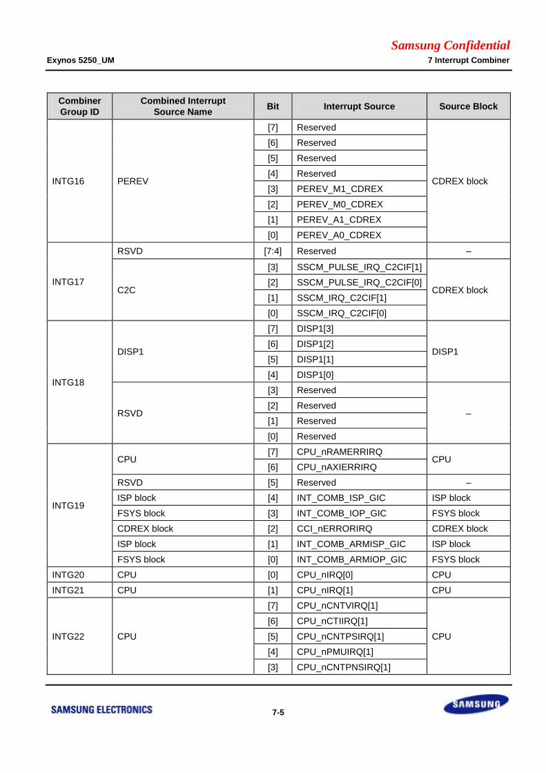
Samsung Confidential Exynos 5250_UM 7 Interrupt Combiner
7-5
Combiner
Group ID
Combined Interrupt
Source Name Bit Interrupt Source Source Block
INTG16 PEREV
[7] Reserved
CDREX block
[6] Reserved
[5] Reserved
[4] Reserved
[3] PEREV_M1_CDREX
[2] PEREV_M0_CDREX
[1] PEREV_A1_CDREX
[0] PEREV_A0_CDREX
INTG17
RSVD [7:4] Reserved –
C2C
[3] SSCM_PULSE_IRQ_C2CIF[1]
CDREX block [2] SSCM_PULSE_IRQ_C2CIF[0]
[1] SSCM_IRQ_C2CIF[1]
[0] SSCM_IRQ_C2CIF[0]
INTG18
DISP1
[7] DISP1[3]
DISP1 [6] DISP1[2]
[5] DISP1[1]
[4] DISP1[0]
RSVD
[3] Reserved
– [2] Reserved
[1] Reserved
[0] Reserved
INTG19
CPU [7] CPU_nRAMERRIRQ
CPU [6] CPU_nAXIERRIRQ
RSVD [5] Reserved –
ISP block [4] INT_COMB_ISP_GIC ISP block
FSYS block [3] INT_COMB_IOP_GIC FSYS block
CDREX block [2] CCI_nERRORIRQ CDREX block
ISP block [1] INT_COMB_ARMISP_GIC ISP block
FSYS block [0] INT_COMB_ARMIOP_GIC FSYS block
INTG20 CPU [0] CPU_nIRQ[0] CPU
INTG21 CPU [1] CPU_nIRQ[1] CPU
INTG22 CPU
[7] CPU_nCNTVIRQ[1]
CPU
[6] CPU_nCTIIRQ[1]
[5] CPU_nCNTPSIRQ[1]
[4] CPU_nPMUIRQ[1]
[3] CPU_nCNTPNSIRQ[1]
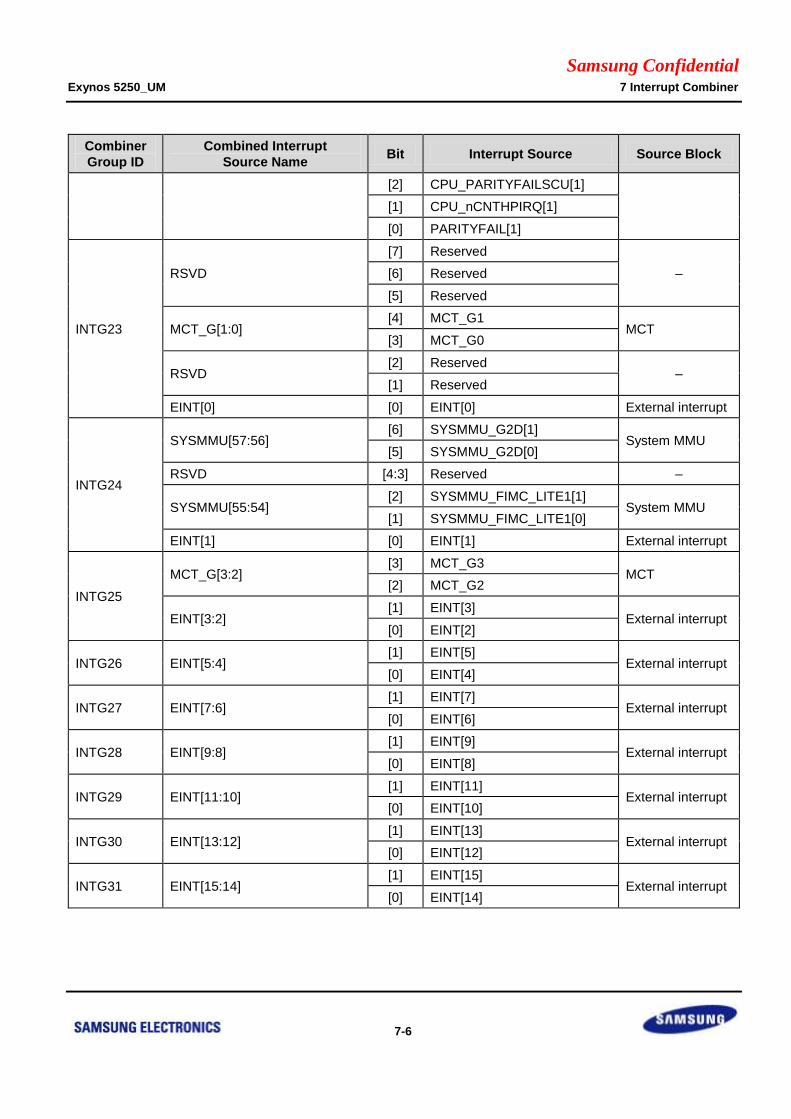
Samsung Confidential Exynos 5250_UM 7 Interrupt Combiner
7-6
Combiner
Group ID
Combined Interrupt
Source Name Bit Interrupt Source Source Block
[2] CPU_PARITYFAILSCU[1]
[1] CPU_nCNTHPIRQ[1]
[0] PARITYFAIL[1]
INTG23
RSVD
[7] Reserved
– [6] Reserved
[5] Reserved
MCT_G[1:0] [4] MCT_G1
MCT [3] MCT_G0
RSVD [2] Reserved
– [1] Reserved
EINT[0] [0] EINT[0] External interrupt
INTG24
SYSMMU[57:56] [6] SYSMMU_G2D[1]
System MMU [5] SYSMMU_G2D[0]
RSVD [4:3] Reserved –
SYSMMU[55:54] [2] SYSMMU_FIMC_LITE1[1]
System MMU [1] SYSMMU_FIMC_LITE1[0]
EINT[1] [0] EINT[1] External interrupt
INTG25
MCT_G[3:2] [3] MCT_G3
MCT [2] MCT_G2
EINT[3:2] [1] EINT[3]
External interrupt [0] EINT[2]
INTG26 EINT[5:4] [1] EINT[5]
External interrupt [0] EINT[4]
INTG27 EINT[7:6] [1] EINT[7]
External interrupt [0] EINT[6]
INTG28 EINT[9:8] [1] EINT[9]
External interrupt [0] EINT[8]
INTG29 EINT[11:10] [1] EINT[11]
External interrupt [0] EINT[10]
INTG30 EINT[13:12] [1] EINT[13]
External interrupt [0] EINT[12]
INTG31 EINT[15:14] [1] EINT[15]
External interrupt [0] EINT[14]

Samsung Confidential Exynos 5250_UM 7 Interrupt Combiner
7-7
7.4 Functional Description
An interrupt enable bit controls an interrupt source in an interrupt group. IESRn registers and IECRn registers
control the interrupt enable bits. IESRn register can toggle an interrupt bit to "1". If you write "1" to a bit position on
IESRn, the corresponding bit on the interrupt enable bits are set to "1". Alternatively, IECRn register can toggle an
interrupt enable bit to "0". If you write "1" to a bit position on IECRn, the corresponding bit on the interrupt enable
bits is cleared to "0". This feature eases the addressing of resource sharing issues in a multi-processor system.
There are several interrupt sources in an interrupt group. If an interrupt enable bit is "0", the corresponding
interrupt is masked. All the interrupt sources in an interrupt group including masked interrupt sources are ORed to
form a combined interrupt request signal. This combined group interrupt request output signal is connected to an
input of a GIC.
ISTRn register reads each interrupt source status before an interrupt enable-bit masks it. The combined group
interrupt request output signal can be shown by reading CIPSR0 register.
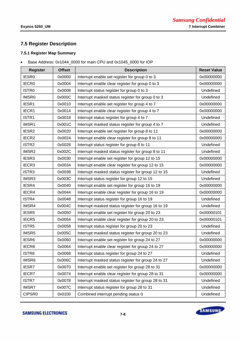
Samsung Confidential Exynos 5250_UM 7 Interrupt Combiner
7-8
7.5 Register Description
7.5.1 Register Map Summary
Base Address: 0x1044_0000 for main CPU and 0x1045_0000 for IOP
Register Offset Description Reset Value
IESR0 0x0000 Interrupt enable set register for group 0 to 3 0x00000000
IECR0 0x0004 Interrupt enable clear register for group 0 to 3 0x00000000
ISTR0 0x0008 Interrupt status register for group 0 to 3 Undefined
IMSR0 0x000C Interrupt masked status register for group 0 to 3 Undefined
IESR1 0x0010 Interrupt enable set register for group 4 to 7 0x00000000
IECR1 0x0014 Interrupt enable clear register for group 4 to 7 0x00000000
ISTR1 0x0018 Interrupt status register for group 4 to 7 Undefined
IMSR1 0x001C Interrupt masked status register for group 4 to 7 Undefined
IESR2 0x0020 Interrupt enable set register for group 8 to 11 0x00000000
IECR2 0x0024 Interrupt enable clear register for group 8 to 11 0x00000000
ISTR2 0x0028 Interrupt status register for group 8 to 11 Undefined
IMSR2 0x002C Interrupt masked status register for group 8 to 11 Undefined
IESR3 0x0030 Interrupt enable set register for group 12 to 15 0x00000000
IECR3 0x0034 Interrupt enable clear register for group 12 to 15 0x00000000
ISTR3 0x0038 Interrupt masked status register for group 12 to 15 Undefined
IMSR3 0x003C Interrupt status register for group 12 to 15 Undefined
IESR4 0x0040 Interrupt enable set register for group 16 to 19 0x00000000
IECR4 0x0044 Interrupt enable clear register for group 16 to 19 0x00000000
ISTR4 0x0048 Interrupt status register for group 16 to 19 Undefined
IMSR4 0x004C Interrupt masked status register for group 16 to 19 Undefined
IESR5 0x0050 Interrupt enable set register for group 20 to 23 0x00000101
IECR5 0x0054 Interrupt enable clear register for group 20 to 23 0x00000101
ISTR5 0x0058 Interrupt status register for group 20 to 23 Undefined
IMSR5 0x005C Interrupt masked status register for group 20 to 23 Undefined
IESR6 0x0060 Interrupt enable set register for group 24 to 27 0x00000000
IECR6 0x0064 Interrupt enable clear register for group 24 to 27 0x00000000
ISTR6 0x0068 Interrupt status register for group 24 to 27 Undefined
IMSR6 0x006C Interrupt masked status register for group 24 to 27 Undefined
IESR7 0x0070 Interrupt enable set register for group 28 to 31 0x00000000
IECR7 0x0074 Interrupt enable clear register for group 28 to 31 0x00000000
ISTR7 0x0078 Interrupt masked status register for group 28 to 31 Undefined
IMSR7 0x007C Interrupt status register for group 28 to 31 Undefined
CIPSR0 0x0100 Combined interrupt pending status 0 Undefined
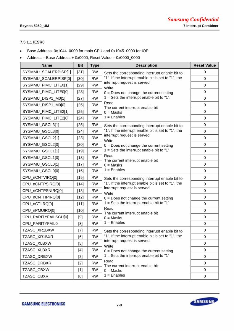
Samsung Confidential Exynos 5250_UM 7 Interrupt Combiner
7-9
7.5.1.1 IESR0
Base Address: 0x1044_0000 for main CPU and 0x1045_0000 for IOP
Address = Base Address + 0x0000, Reset Value = 0x0000_0000
Name Bit Type Description Reset Value
SYSMMU_SCALERPISP[1] [31] RW Sets the corresponding interrupt enable bit to
"1". If the interrupt enable bit is set to "1", the
interrupt request is served.
Write
0 = Does not change the current setting
1 = Sets the interrupt enable bit to "1".
Read
The current interrupt enable bit
0 = Masks
1 = Enables
0
SYSMMU_SCALERPISP[0] [30] RW 0
SYSMMU_FIMC_LITE0[1] [29] RW 0
SYSMMU_FIMC_LITE0[0] [28] RW 0
SYSMMU_DISP1_M0[1] [27] RW 0
SYSMMU_DISP1_M0[0] [26] RW 0
SYSMMU_FIMC_LITE2[1] [25] RW 0
SYSMMU_FIMC_LITE2[0] [24] RW 0
SYSMMU_GSCL3[1] [25] RW Sets the corresponding interrupt enable bit to
"1". If the interrupt enable bit is set to "1", the
interrupt request is served.
Write
0 = Does not change the current setting
1 = Sets the interrupt enable bit to "1"
Read
The current interrupt enable bit
0 = Masks
1 = Enables
0
SYSMMU_GSCL3[0] [24] RW 0
SYSMMU_GSCL2[1] [23] RW 0
SYSMMU_GSCL2[0] [20] RW 0
SYSMMU_GSCL1[1] [19] RW 0
SYSMMU_GSCL1[0] [18] RW 0
SYSMMU_GSCL0[1] [17] RW 0
SYSMMU_GSCL0[0] [16] RW 0
CPU_nCNTVIRQ[0] [15] RW Sets the corresponding interrupt enable bit to
"1". If the interrupt enable bit is set to "1", the
interrupt request is served.
Write
0 = Does not change the current setting
1 = Sets the interrupt enable bit to "1"
Read
The current interrupt enable bit
0 = Masks
1 = Enables
0
CPU_nCNTPSIRQ[0] [14] RW 0
CPU_nCNTPSNIRQ[0] [13] RW 0
CPU_nCNTHPIRQ[0] [12] RW 0
CPU_nCTIIRQ[0] [11] RW 0
CPU_nPMUIRQ[0] [10] RW 0
CPU_PARITYFAILSCU[0] [9] RW 0
CPU_PARITYFAIL0 [8] RW 0
TZASC_XR1BXW [7] RW Sets the corresponding interrupt enable bit to
"1". If the interrupt enable bit is set to "1", the
interrupt request is served.
Write
0 = Does not change the current setting
1 = Sets the interrupt enable bit to "1"
Read
The current interrupt enable bit
0 = Masks
1 = Enables
0
TZASC_XR1BXR [6] RW 0
TZASC_XLBXW [5] RW 0
TZASC_XLBXR [4] RW 0
TZASC_DRBXW [3] RW 0
TZASC_DRBXR [2] RW 0
TZASC_CBXW [1] RW 0
TZASC_CBXR [0] RW 0
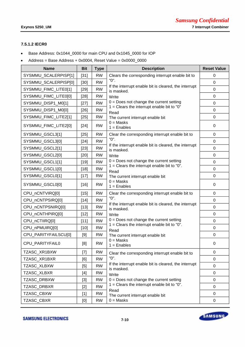
Samsung Confidential Exynos 5250_UM 7 Interrupt Combiner
7-10
7.5.1.2 IECR0
Base Address: 0x1044_0000 for main CPU and 0x1045_0000 for IOP
Address = Base Address + 0x0004, Reset Value = 0x0000_0000
Name Bit Type Description Reset Value
SYSMMU_SCALERPISP[1] [31] RW Clears the corresponding interrupt enable bit to
"0".
If the interrupt enable bit is cleared, the interrupt
is masked.
Write
0 = Does not change the current setting
1 = Clears the interrupt enable bit to "0"
Read
The current interrupt enable bit
0 = Masks
1 = Enables
0
SYSMMU_SCALERPISP[0] [30] RW 0
SYSMMU_FIMC_LITE0[1] [29] RW 0
SYSMMU_FIMC_LITE0[0] [28] RW 0
SYSMMU_DISP1_M0[1] [27] RW 0
SYSMMU_DISP1_M0[0] [26] RW 0
SYSMMU_FIMC_LITE2[1] [25] RW 0
SYSMMU_FIMC_LITE2[0] [24] RW 0
SYSMMU_GSCL3[1] [25] RW Clear the corresponding interrupt enable bit to
"0".
If the interrupt enable bit is cleared, the interrupt
is masked.
Write
0 = Does not change the current setting
1 = Clears the interrupt enable bit to "0".
Read
The current interrupt enable bit
0 = Masks
1 = Enables
0
SYSMMU_GSCL3[0] [24] RW 0
SYSMMU_GSCL2[1] [23] RW 0
SYSMMU_GSCL2[0] [20] RW 0
SYSMMU_GSCL1[1] [19] RW 0
SYSMMU_GSCL1[0] [18] RW 0
SYSMMU_GSCL0[1] [17] RW 0
SYSMMU_GSCL0[0] [16] RW 0
CPU_nCNTVIRQ[0] [15] RW Clear the corresponding interrupt enable bit to
"0".
If the interrupt enable bit is cleared, the interrupt
is masked.
Write
0 = Does not change the current setting
1 = Clears the interrupt enable bit to "0".
Read
The current interrupt enable bit
0 = Masks
1 = Enables
0
CPU_nCNTPSIRQ[0] [14] RW 0
CPU_nCNTPSNIRQ[0] [13] RW 0
CPU_nCNTHPIRQ[0] [12] RW 0
CPU_nCTIIRQ[0] [11] RW 0
CPU_nPMUIRQ[0] [10] RW 0
CPU_PARITYFAILSCU[0] [9] RW 0
CPU_PARITYFAIL0 [8] RW 0
TZASC_XR1BXW [7] RW Clear the corresponding interrupt enable bit to
"0".
If the interrupt enable bit is cleared, the interrupt
is masked.
Write
0 = Does not change the current setting
1 = Clears the interrupt enable bit to "0".
Read
The current interrupt enable bit
0 = Masks
0
TZASC_XR1BXR [6] RW 0
TZASC_XLBXW [5] RW 0
TZASC_XLBXR [4] RW 0
TZASC_DRBXW [3] RW 0
TZASC_DRBXR [2] RW 0
TZASC_CBXW [1] RW 0
TZASC_CBXR [0] RW 0

Samsung Confidential Exynos 5250_UM 7 Interrupt Combiner
7-11
Name Bit Type Description Reset Value
1 = Enables
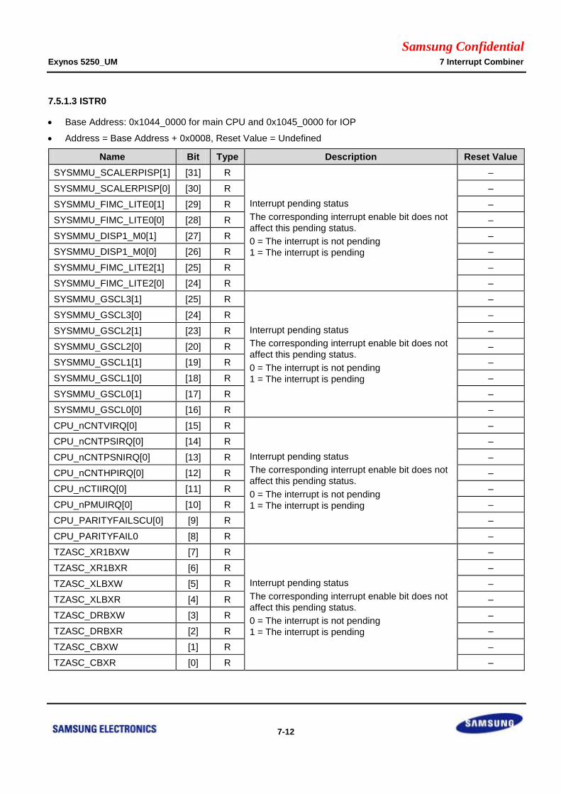
Samsung Confidential Exynos 5250_UM 7 Interrupt Combiner
7-12
7.5.1.3 ISTR0
Base Address: 0x1044_0000 for main CPU and 0x1045_0000 for IOP
Address = Base Address + 0x0008, Reset Value = Undefined
Name Bit Type Description Reset Value
SYSMMU_SCALERPISP[1] [31] R
Interrupt pending status
The corresponding interrupt enable bit does not
affect this pending status.
0 = The interrupt is not pending
1 = The interrupt is pending
–
SYSMMU_SCALERPISP[0] [30] R –
SYSMMU_FIMC_LITE0[1] [29] R –
SYSMMU_FIMC_LITE0[0] [28] R –
SYSMMU_DISP1_M0[1] [27] R –
SYSMMU_DISP1_M0[0] [26] R –
SYSMMU_FIMC_LITE2[1] [25] R –
SYSMMU_FIMC_LITE2[0] [24] R –
SYSMMU_GSCL3[1] [25] R
Interrupt pending status
The corresponding interrupt enable bit does not
affect this pending status.
0 = The interrupt is not pending
1 = The interrupt is pending
–
SYSMMU_GSCL3[0] [24] R –
SYSMMU_GSCL2[1] [23] R –
SYSMMU_GSCL2[0] [20] R –
SYSMMU_GSCL1[1] [19] R –
SYSMMU_GSCL1[0] [18] R –
SYSMMU_GSCL0[1] [17] R –
SYSMMU_GSCL0[0] [16] R –
CPU_nCNTVIRQ[0] [15] R
Interrupt pending status
The corresponding interrupt enable bit does not
affect this pending status.
0 = The interrupt is not pending
1 = The interrupt is pending
–
CPU_nCNTPSIRQ[0] [14] R –
CPU_nCNTPSNIRQ[0] [13] R –
CPU_nCNTHPIRQ[0] [12] R –
CPU_nCTIIRQ[0] [11] R –
CPU_nPMUIRQ[0] [10] R –
CPU_PARITYFAILSCU[0] [9] R –
CPU_PARITYFAIL0 [8] R –
TZASC_XR1BXW [7] R
Interrupt pending status
The corresponding interrupt enable bit does not
affect this pending status.
0 = The interrupt is not pending
1 = The interrupt is pending
–
TZASC_XR1BXR [6] R –
TZASC_XLBXW [5] R –
TZASC_XLBXR [4] R –
TZASC_DRBXW [3] R –
TZASC_DRBXR [2] R –
TZASC_CBXW [1] R –
TZASC_CBXR [0] R –
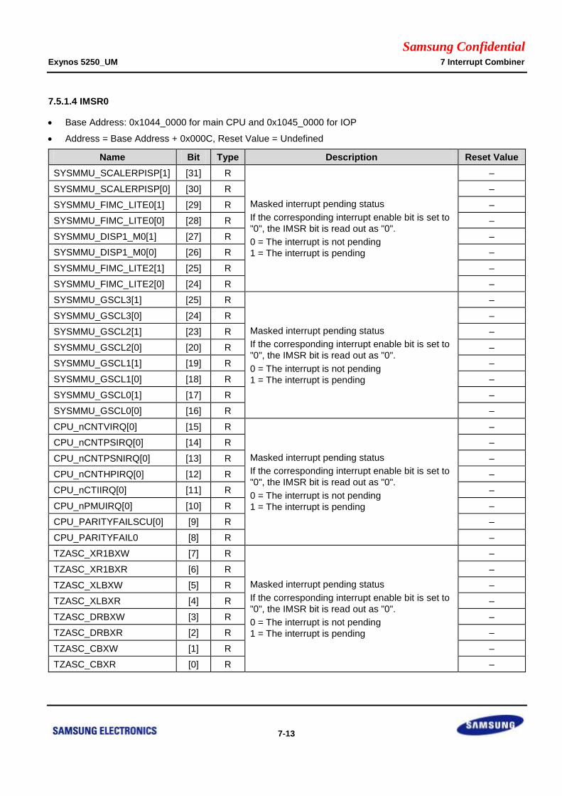
Samsung Confidential Exynos 5250_UM 7 Interrupt Combiner
7-13
7.5.1.4 IMSR0
Base Address: 0x1044_0000 for main CPU and 0x1045_0000 for IOP
Address = Base Address + 0x000C, Reset Value = Undefined
Name Bit Type Description Reset Value
SYSMMU_SCALERPISP[1] [31] R
Masked interrupt pending status
If the corresponding interrupt enable bit is set to
"0", the IMSR bit is read out as "0".
0 = The interrupt is not pending
1 = The interrupt is pending
–
SYSMMU_SCALERPISP[0] [30] R –
SYSMMU_FIMC_LITE0[1] [29] R –
SYSMMU_FIMC_LITE0[0] [28] R –
SYSMMU_DISP1_M0[1] [27] R –
SYSMMU_DISP1_M0[0] [26] R –
SYSMMU_FIMC_LITE2[1] [25] R –
SYSMMU_FIMC_LITE2[0] [24] R –
SYSMMU_GSCL3[1] [25] R
Masked interrupt pending status
If the corresponding interrupt enable bit is set to
"0", the IMSR bit is read out as "0".
0 = The interrupt is not pending
1 = The interrupt is pending
–
SYSMMU_GSCL3[0] [24] R –
SYSMMU_GSCL2[1] [23] R –
SYSMMU_GSCL2[0] [20] R –
SYSMMU_GSCL1[1] [19] R –
SYSMMU_GSCL1[0] [18] R –
SYSMMU_GSCL0[1] [17] R –
SYSMMU_GSCL0[0] [16] R –
CPU_nCNTVIRQ[0] [15] R
Masked interrupt pending status
If the corresponding interrupt enable bit is set to
"0", the IMSR bit is read out as "0".
0 = The interrupt is not pending
1 = The interrupt is pending
–
CPU_nCNTPSIRQ[0] [14] R –
CPU_nCNTPSNIRQ[0] [13] R –
CPU_nCNTHPIRQ[0] [12] R –
CPU_nCTIIRQ[0] [11] R –
CPU_nPMUIRQ[0] [10] R –
CPU_PARITYFAILSCU[0] [9] R –
CPU_PARITYFAIL0 [8] R –
TZASC_XR1BXW [7] R
Masked interrupt pending status
If the corresponding interrupt enable bit is set to
"0", the IMSR bit is read out as "0".
0 = The interrupt is not pending
1 = The interrupt is pending
–
TZASC_XR1BXR [6] R –
TZASC_XLBXW [5] R –
TZASC_XLBXR [4] R –
TZASC_DRBXW [3] R –
TZASC_DRBXR [2] R –
TZASC_CBXW [1] R –
TZASC_CBXR [0] R –
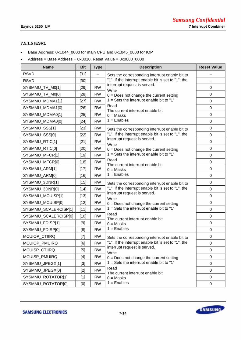
Samsung Confidential Exynos 5250_UM 7 Interrupt Combiner
7-14
7.5.1.5 IESR1
Base Address: 0x1044_0000 for main CPU and 0x1045_0000 for IOP
Address = Base Address + 0x0010, Reset Value = 0x0000_0000
Name Bit Type Description Reset Value
RSVD [31] – Sets the corresponding interrupt enable bit to
"1". If the interrupt enable bit is set to "1", the
interrupt request is served.
Write
0 = Does not change the current setting
1 = Sets the interrupt enable bit to "1"
Read
The current interrupt enable bit
0 = Masks
1 = Enables
–
RSVD [30] – –
SYSMMU_TV_M0[1] [29] RW 0
SYSMMU_TV_M0[0] [28] RW 0
SYSMMU_MDMA1[1] [27] RW 0
SYSMMU_MDMA1[0] [26] RW 0
SYSMMU_MDMA0[1] [25] RW 0
SYSMMU_MDMA0[0] [24] RW 0
SYSMMU_SSS[1] [23] RW Sets the corresponding interrupt enable bit to
"1". If the interrupt enable bit is set to "1", the
interrupt request is served.
Write
0 = Does not change the current setting
1 = Sets the interrupt enable bit to "1"
Read
The current interrupt enable bit
0 = Masks
1 = Enables
0
SYSMMU_SSS[0] [22] RW 0
SYSMMU_RTIC[1] [21] RW 0
SYSMMU_RTIC[0] [20] RW 0
SYSMMU_MFCR[1] [19] RW 0
SYSMMU_MFCR[0] [18] RW 0
SYSMMU_ARM[1] [17] RW 0
SYSMMU_ARM[0] [16] RW 0
SYSMMU_3DNR[1] [15] RW Sets the corresponding interrupt enable bit to
"1". If the interrupt enable bit is set to "1", the
interrupt request is served.
Write
0 = Does not change the current setting
1 = Sets the interrupt enable bit to "1"
Read
The current interrupt enable bit
0 = Masks
1 = Enables
0
SYSMMU_3DNR[0] [14] RW 0
SYSMMU_MCUISP[1] [13] RW 0
SYSMMU_MCUISP[0] [12] RW 0
SYSMMU_SCALERCISP[1] [11] RW 0
SYSMMU_SCALERCISP[0] [10] RW 0
SYSMMU_FDISP[1] [9] RW 0
SYSMMU_FDISP[0] [8] RW 0
MCUIOP_CTIIRQ [7] RW Sets the corresponding interrupt enable bit to
"1". If the interrupt enable bit is set to "1", the
interrupt request is served.
Write
0 = Does not change the current setting
1 = Sets the interrupt enable bit to "1"
Read
The current interrupt enable bit
0 = Masks
1 = Enables
0
MCUIOP_PMUIRQ [6] RW 0
MCUISP_CTIIRQ [5] RW 0
MCUISP_PMUIRQ [4] RW 0
SYSMMU_JPEGX[1] [3] RW 0
SYSMMU_JPEGX[0] [2] RW 0
SYSMMU_ROTATOR[1] [1] RW 0
SYSMMU_ROTATOR[0] [0] RW 0

Samsung Confidential Exynos 5250_UM 7 Interrupt Combiner
7-15
7.5.1.6 IECR1
Base Address: 0x1044_0000 for main CPU and 0x1045_0000 for IOP
Address = Base Address + 0x0014, Reset Value = 0x0000_0000
Name Bit Type Description Reset Value
RSVD [31] – Clear the corresponding interrupt enable bit to
"0". If the interrupt enable bit is cleared, the
interrupt is masked.
Write
0 = Does not change the current setting
1 = Clears the interrupt enable bit to "0"
Read
The current interrupt enable bit
0 = Masks
1 = Enables
–
RSVD [30] – –
SYSMMU_TV_M0[1] [29] RW 0
SYSMMU_TV_M0[0] [28] RW 0
SYSMMU_MDMA1[1] [27] RW 0
SYSMMU_MDMA1[0] [26] RW 0
SYSMMU_MDMA0[1] [25] RW 0
SYSMMU_MDMA0[0] [24] RW 0
SYSMMU_SSS[1] [23] RW Clear the corresponding interrupt enable bit to
"0". If the interrupt enable bit is cleared, the
interrupt is masked.
Write
0 = Does not change the current setting
1 = Clears the interrupt enable bit to "0"
Read
The current interrupt enable bit
0 = Masks
1 = Enabled
0
SYSMMU_SSS[0] [22] RW 0
SYSMMU_RTIC[1] [21] RW 0
SYSMMU_RTIC[0] [20] RW 0
SYSMMU_MFCR[1] [19] RW 0
SYSMMU_MFCR[0] [18] RW 0
SYSMMU_ARM[1] [17] RW 0
SYSMMU_ARM[0] [16] RW 0
SYSMMU_3DNR[1] [15] RW Clear the corresponding interrupt enable bit to
"0". If the interrupt enable bit is cleared, the
interrupt is masked.
Write
0 = Does not change the current setting
1 = Clears the interrupt enable bit to "0"
Read
The current interrupt enable bit
0 = Masks
1 = Enabled
0
SYSMMU_3DNR[0] [14] RW 0
SYSMMU_MCUISP[1] [13] RW 0
SYSMMU_MCUISP[0] [12] RW 0
SYSMMU_SCALERCISP[1] [11] RW 0
SYSMMU_SCALERCISP[0] [10] RW 0
SYSMMU_FDISP[1] [9] RW 0
SYSMMU_FDISP[0] [8] RW 0
MCUIOP_CTIIRQ [7] RW Clear the corresponding interrupt enable bit to
"0". If the interrupt enable bit is cleared, the
interrupt is masked.
Write
0 = Does not change the current setting
1 = Clears the interrupt enable bit to "0"
Read
The current interrupt enable bit
0 = Masks
1 = Enabled
0
MCUIOP_PMUIRQ [6] RW 0
MCUISP_CTIIRQ [5] RW 0
MCUISP_PMUIRQ [4] RW 0
SYSMMU_JPEGX[1] [3] RW 0
SYSMMU_JPEGX[0] [2] RW 0
SYSMMU_ROTATOR[1] [1] RW 0
SYSMMU_ROTATOR[0] [0] RW 0

Samsung Confidential Exynos 5250_UM 7 Interrupt Combiner
7-16
7.5.1.7 ISTR1
Base Address: 0x1044_0000 for main CPU and 0x1045_0000 for IOP
Address = Base Address + 0x0018, Reset Value = Undefined
Name Bit Type Description Reset Value
RSVD [31] –
Interrupt pending status
The corresponding interrupt enable bit does not
affect this pending status.
0 = The interrupt is not pending
1 = The interrupt is pending
–
RSVD [30] – –
SYSMMU_TV_M0[1] [29] R –
SYSMMU_TV_M0[0] [28] R –
SYSMMU_MDMA1[1] [27] R –
SYSMMU_MDMA1[0] [26] R –
SYSMMU_MDMA0[1] [25] R –
SYSMMU_MDMA0[0] [24] R –
SYSMMU_SSS[1] [23] R
Interrupt pending status
The corresponding interrupt enable bit does not
affect this pending status.
0 = The interrupt is not pending
1 = The interrupt is pending
–
SYSMMU_SSS[0] [22] R –
SYSMMU_RTIC[1] [21] R –
SYSMMU_RTIC[0] [20] R –
SYSMMU_MFCR[1] [19] R –
SYSMMU_MFCR[0] [18] R –
SYSMMU_ARM[1] [17] R –
SYSMMU_ARM[0] [16] R –
SYSMMU_3DNR[1] [15] R
Interrupt pending status
The corresponding interrupt enable bit does not
affect this pending status.
0 = The interrupt is not pending
1 = The interrupt is pending
–
SYSMMU_3DNR[0] [14] R –
SYSMMU_MCUISP[1] [13] R –
SYSMMU_MCUISP[0] [12] R –
SYSMMU_SCALERCISP[1] [11] R –
SYSMMU_SCALERCISP[0] [10] R –
SYSMMU_FDISP[1] [9] R –
SYSMMU_FDISP[0] [8] R –
MCUIOP_CTIIRQ [7] R
Interrupt pending status
The corresponding interrupt enable bit does not
affect this pending status.
0 = The interrupt is not pending
1 = The interrupt is pending
–
MCUIOP_PMUIRQ [6] R –
MCUISP_CTIIRQ [5] R –
MCUISP_PMUIRQ [4] R –
SYSMMU_JPEGX[1] [3] R –
SYSMMU_JPEGX[0] [2] R –
SYSMMU_ROTATOR[1] [1] R –
SYSMMU_ROTATOR[0] [0] R –
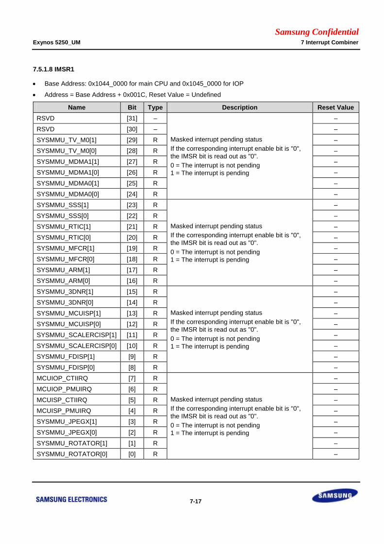
Samsung Confidential Exynos 5250_UM 7 Interrupt Combiner
7-17
7.5.1.8 IMSR1
Base Address: 0x1044_0000 for main CPU and 0x1045_0000 for IOP
Address = Base Address + 0x001C, Reset Value = Undefined
Name Bit Type Description Reset Value
RSVD [31] –
Masked interrupt pending status
If the corresponding interrupt enable bit is "0",
the IMSR bit is read out as "0".
0 = The interrupt is not pending
1 = The interrupt is pending
–
RSVD [30] – –
SYSMMU_TV_M0[1] [29] R –
SYSMMU_TV_M0[0] [28] R –
SYSMMU_MDMA1[1] [27] R –
SYSMMU_MDMA1[0] [26] R –
SYSMMU_MDMA0[1] [25] R –
SYSMMU_MDMA0[0] [24] R –
SYSMMU_SSS[1] [23] R
Masked interrupt pending status
If the corresponding interrupt enable bit is "0",
the IMSR bit is read out as "0".
0 = The interrupt is not pending
1 = The interrupt is pending
–
SYSMMU_SSS[0] [22] R –
SYSMMU_RTIC[1] [21] R –
SYSMMU_RTIC[0] [20] R –
SYSMMU_MFCR[1] [19] R –
SYSMMU_MFCR[0] [18] R –
SYSMMU_ARM[1] [17] R –
SYSMMU_ARM[0] [16] R –
SYSMMU_3DNR[1] [15] R
Masked interrupt pending status
If the corresponding interrupt enable bit is "0",
the IMSR bit is read out as "0".
0 = The interrupt is not pending
1 = The interrupt is pending
–
SYSMMU_3DNR[0] [14] R –
SYSMMU_MCUISP[1] [13] R –
SYSMMU_MCUISP[0] [12] R –
SYSMMU_SCALERCISP[1] [11] R –
SYSMMU_SCALERCISP[0] [10] R –
SYSMMU_FDISP[1] [9] R –
SYSMMU_FDISP[0] [8] R –
MCUIOP_CTIIRQ [7] R
Masked interrupt pending status
If the corresponding interrupt enable bit is "0",
the IMSR bit is read out as "0".
0 = The interrupt is not pending
1 = The interrupt is pending
–
MCUIOP_PMUIRQ [6] R –
MCUISP_CTIIRQ [5] R –
MCUISP_PMUIRQ [4] R –
SYSMMU_JPEGX[1] [3] R –
SYSMMU_JPEGX[0] [2] R –
SYSMMU_ROTATOR[1] [1] R –
SYSMMU_ROTATOR[0] [0] R –
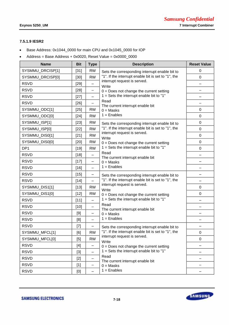
Samsung Confidential Exynos 5250_UM 7 Interrupt Combiner
7-18
7.5.1.9 IESR2
Base Address: 0x1044_0000 for main CPU and 0x1045_0000 for IOP
Address = Base Address + 0x0020, Reset Value = 0x0000_0000
Name Bit Type Description Reset Value
SYSMMU_DRCISP[1] [31] RW Sets the corresponding interrupt enable bit to
"1". If the interrupt enable bit is set to "1", the
interrupt request is served.
Write
0 = Does not change the current setting
1 = Sets the interrupt enable bit to "1"
Read
The current interrupt enable bit
0 = Masks
1 = Enables
0
SYSMMU_DRCISP[0] [30] RW 0
RSVD [29] – –
RSVD [28] – –
RSVD [27] – –
RSVD [26] – –
SYSMMU_ODC[1] [25] RW 0
SYSMMU_ODC[0] [24] RW 0
SYSMMU_ISP[1] [23] RW Sets the corresponding interrupt enable bit to
"1". If the interrupt enable bit is set to "1", the
interrupt request is served.
Write
0 = Does not change the current setting
1 = Sets the interrupt enable bit to "1"
Read
The current interrupt enable bit
0 = Masks
1 = Enables
0
SYSMMU_ISP[0] [22] RW 0
SYSMMU_DIS0[1] [21] RW 0
SYSMMU_DIS0[0] [20] RW 0
DP1 [19] RW 0
RSVD [18] – –
RSVD [17] – –
RSVD [16] – –
RSVD [15] – Sets the corresponding interrupt enable bit to
"1". If the interrupt enable bit is set to "1", the
interrupt request is served.
Write
0 = Does not change the current setting
1 = Sets the interrupt enable bit to "1"
Read
The current interrupt enable bit
0 = Masks
1 = Enables
–
RSVD [14] – –
SYSMMU_DIS1[1] [13] RW 0
SYSMMU_DIS1[0] [12] RW 0
RSVD [11] – –
RSVD [10] – –
RSVD [9] – –
RSVD [8] – –
RSVD [7] – Sets the corresponding interrupt enable bit to
"1". If the interrupt enable bit is set to "1", the
interrupt request is served.
Write
0 = Does not change the current setting
1 = Sets the interrupt enable bit to "1"
Read
The current interrupt enable bit
0 = Masks
1 = Enables
–
SYSMMU_MFCL[1] [6] RW 0
SYSMMU_MFCL[0] [5] RW 0
RSVD [4] – –
RSVD [3] – –
RSVD [2] – –
RSVD [1] – –
RSVD [0] – –
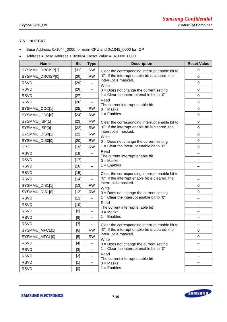
Samsung Confidential Exynos 5250_UM 7 Interrupt Combiner
7-19
7.5.1.10 IECR2
Base Address: 0x1044_0000 for main CPU and 0x1045_0000 for IOP
Address = Base Address + 0x0024, Reset Value = 0x0000_0000
Name Bit Type Description Reset Value
SYSMMU_DRCISP[1] [31] RW Clear the corresponding interrupt enable bit to
"0". If the interrupt enable bit is cleared, the
interrupt is masked.
Write
0 = Does not change the current setting
1 = Clear the interrupt enable bit to "0"
Read
The current interrupt enable bit
0 = Masks
1 = Enables
0
SYSMMU_DRCISP[0] [30] RW 0
RSVD [29] – 0
RSVD [28] – 0
RSVD [27] – 0
RSVD [26] – 0
SYSMMU_ODC[1] [25] RW 0
SYSMMU_ODC[0] [24] RW 0
SYSMMU_ISP[1] [23] RW Clear the corresponding interrupt enable bit to
"0". If the interrupt enable bit is cleared, the
interrupt is masked.
Write
0 = Does not change the current setting
1 = Clear the interrupt enable bit to "0"
Read
The current interrupt enable bit
0 = Masks
1 = Enables
0
SYSMMU_ISP[0] [22] RW 0
SYSMMU_DIS0[1] [21] RW 0
SYSMMU_DIS0[0] [20] RW 0
DP1 [19] RW 0
RSVD [18] – –
RSVD [17] – –
RSVD [16] – –
RSVD [15] – Clear the corresponding interrupt enable bit to
"0". If the interrupt enable bit is cleared, the
interrupt is masked.
Write
0 = Does not change the current setting
1 = Clear the interrupt enable bit to "0"
Read
The current interrupt enable bit
0 = Masks
1 = Enables
–
RSVD [14] – –
SYSMMU_DIS1[1] [13] RW 0
SYSMMU_DIS1[0] [12] RW 0
RSVD [11] – –
RSVD [10] – –
RSVD [9] – –
RSVD [8] – –
RSVD [7] – Clear the corresponding interrupt enable bit to
"0". If the interrupt enable bit is cleared, the
interrupt is masked.
Write
0 = Does not change the current setting
1 = Clear the interrupt enable bit to "0"
Read
The current interrupt enable bit
0 = Masks
1 = Enables
–
SYSMMU_MFCL[1] [6] RW 0
SYSMMU_MFCL[0] [5] RW 0
RSVD [4] – –
RSVD [3] – –
RSVD [2] – –
RSVD [1] – –
RSVD [0] – –
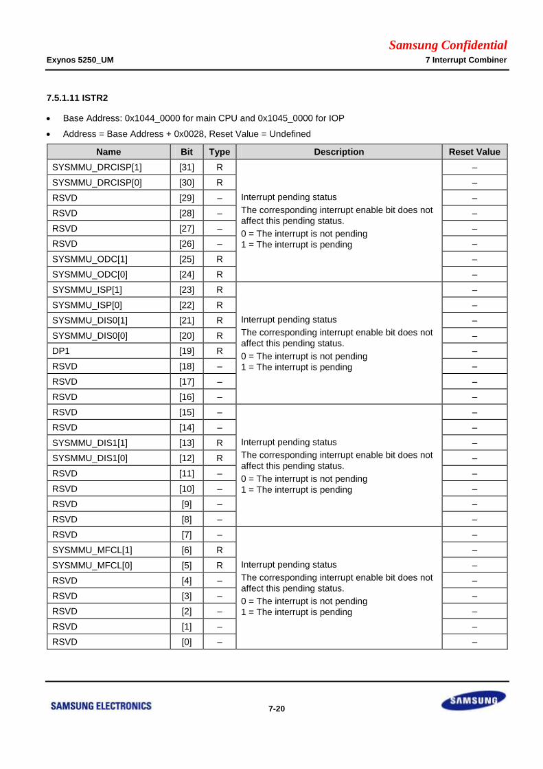
Samsung Confidential Exynos 5250_UM 7 Interrupt Combiner
7-20
7.5.1.11 ISTR2
Base Address: 0x1044_0000 for main CPU and 0x1045_0000 for IOP
Address = Base Address + 0x0028, Reset Value = Undefined
Name Bit Type Description Reset Value
SYSMMU_DRCISP[1] [31] R
Interrupt pending status
The corresponding interrupt enable bit does not
affect this pending status.
0 = The interrupt is not pending
1 = The interrupt is pending
–
SYSMMU_DRCISP[0] [30] R –
RSVD [29] – –
RSVD [28] – –
RSVD [27] – –
RSVD [26] – –
SYSMMU_ODC[1] [25] R –
SYSMMU_ODC[0] [24] R –
SYSMMU_ISP[1] [23] R
Interrupt pending status
The corresponding interrupt enable bit does not
affect this pending status.
0 = The interrupt is not pending
1 = The interrupt is pending
–
SYSMMU_ISP[0] [22] R –
SYSMMU_DIS0[1] [21] R –
SYSMMU_DIS0[0] [20] R –
DP1 [19] R –
RSVD [18] – –
RSVD [17] – –
RSVD [16] – –
RSVD [15] –
Interrupt pending status
The corresponding interrupt enable bit does not
affect this pending status.
0 = The interrupt is not pending
1 = The interrupt is pending
–
RSVD [14] – –
SYSMMU_DIS1[1] [13] R –
SYSMMU_DIS1[0] [12] R –
RSVD [11] – –
RSVD [10] – –
RSVD [9] – –
RSVD [8] – –
RSVD [7] –
Interrupt pending status
The corresponding interrupt enable bit does not
affect this pending status.
0 = The interrupt is not pending
1 = The interrupt is pending
–
SYSMMU_MFCL[1] [6] R –
SYSMMU_MFCL[0] [5] R –
RSVD [4] – –
RSVD [3] – –
RSVD [2] – –
RSVD [1] – –
RSVD [0] – –
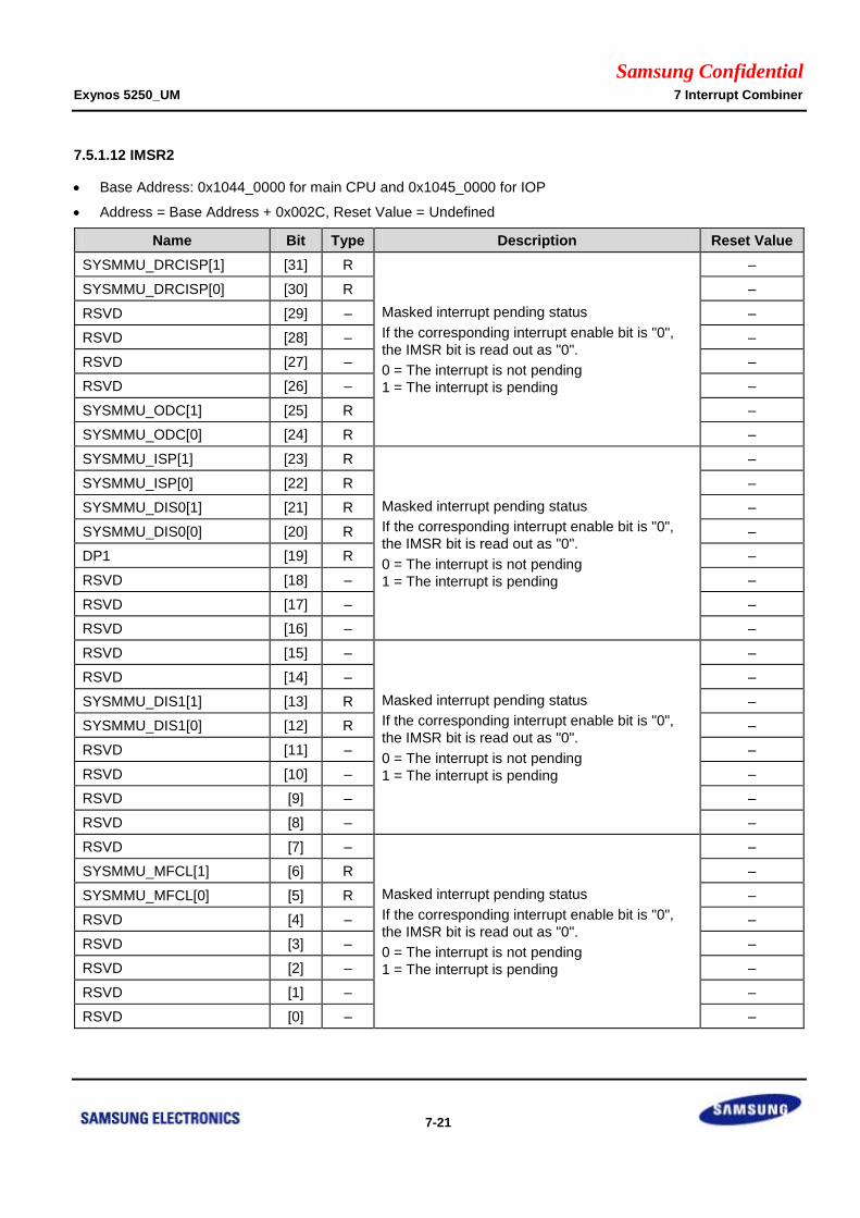
Samsung Confidential Exynos 5250_UM 7 Interrupt Combiner
7-21
7.5.1.12 IMSR2
Base Address: 0x1044_0000 for main CPU and 0x1045_0000 for IOP
Address = Base Address + 0x002C, Reset Value = Undefined
Name Bit Type Description Reset Value
SYSMMU_DRCISP[1] [31] R
Masked interrupt pending status
If the corresponding interrupt enable bit is "0",
the IMSR bit is read out as "0".
0 = The interrupt is not pending
1 = The interrupt is pending
–
SYSMMU_DRCISP[0] [30] R –
RSVD [29] – –
RSVD [28] – –
RSVD [27] – –
RSVD [26] – –
SYSMMU_ODC[1] [25] R –
SYSMMU_ODC[0] [24] R –
SYSMMU_ISP[1] [23] R
Masked interrupt pending status
If the corresponding interrupt enable bit is "0",
the IMSR bit is read out as "0".
0 = The interrupt is not pending
1 = The interrupt is pending
–
SYSMMU_ISP[0] [22] R –
SYSMMU_DIS0[1] [21] R –
SYSMMU_DIS0[0] [20] R –
DP1 [19] R –
RSVD [18] – –
RSVD [17] – –
RSVD [16] – –
RSVD [15] –
Masked interrupt pending status
If the corresponding interrupt enable bit is "0",
the IMSR bit is read out as "0".
0 = The interrupt is not pending
1 = The interrupt is pending
–
RSVD [14] – –
SYSMMU_DIS1[1] [13] R –
SYSMMU_DIS1[0] [12] R –
RSVD [11] – –
RSVD [10] – –
RSVD [9] – –
RSVD [8] – –
RSVD [7] –
Masked interrupt pending status
If the corresponding interrupt enable bit is "0",
the IMSR bit is read out as "0".
0 = The interrupt is not pending
1 = The interrupt is pending
–
SYSMMU_MFCL[1] [6] R –
SYSMMU_MFCL[0] [5] R –
RSVD [4] – –
RSVD [3] – –
RSVD [2] – –
RSVD [1] – –
RSVD [0] – –
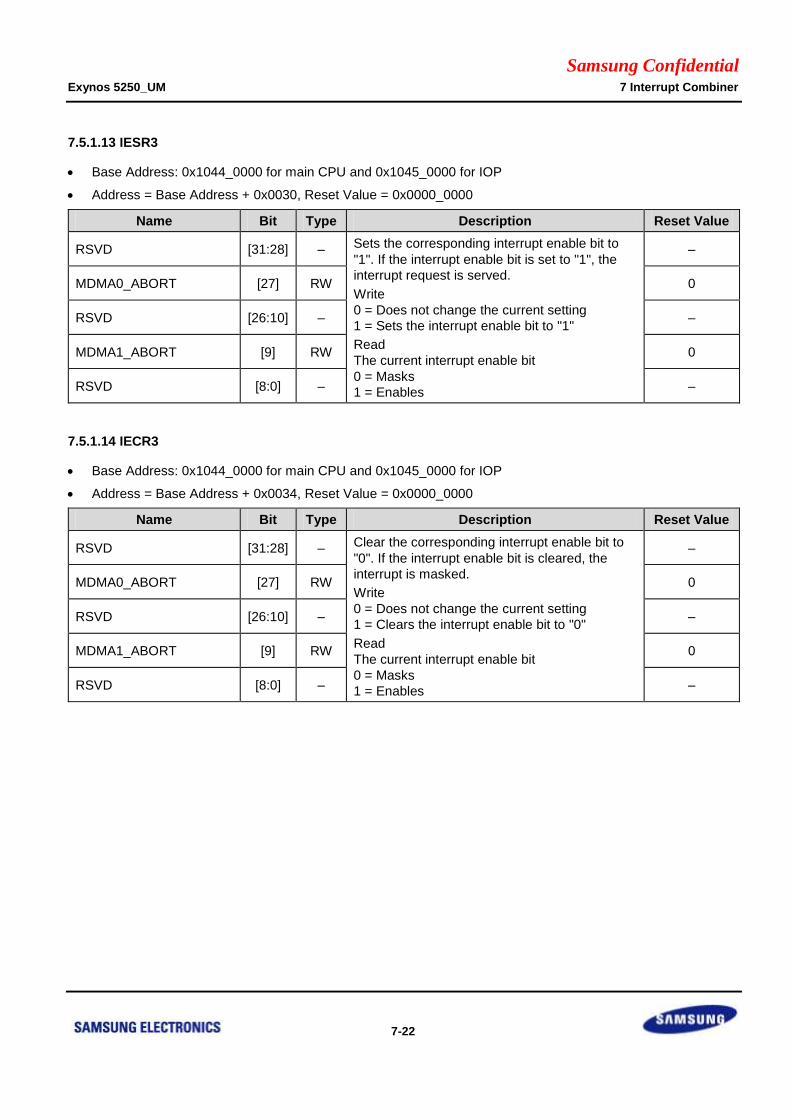
Samsung Confidential Exynos 5250_UM 7 Interrupt Combiner
7-22
7.5.1.13 IESR3
Base Address: 0x1044_0000 for main CPU and 0x1045_0000 for IOP
Address = Base Address + 0x0030, Reset Value = 0x0000_0000
Name Bit Type Description Reset Value
RSVD [31:28] – Sets the corresponding interrupt enable bit to
"1". If the interrupt enable bit is set to "1", the
interrupt request is served.
Write
0 = Does not change the current setting
1 = Sets the interrupt enable bit to "1"
Read
The current interrupt enable bit
0 = Masks
1 = Enables
–
MDMA0_ABORT [27] RW 0
RSVD [26:10] – –
MDMA1_ABORT [9] RW 0
RSVD [8:0] – –
7.5.1.14 IECR3
Base Address: 0x1044_0000 for main CPU and 0x1045_0000 for IOP
Address = Base Address + 0x0034, Reset Value = 0x0000_0000
Name Bit Type Description Reset Value
RSVD [31:28] – Clear the corresponding interrupt enable bit to
"0". If the interrupt enable bit is cleared, the
interrupt is masked.
Write
0 = Does not change the current setting
1 = Clears the interrupt enable bit to "0"
Read
The current interrupt enable bit
0 = Masks
1 = Enables
–
MDMA0_ABORT [27] RW 0
RSVD [26:10] – –
MDMA1_ABORT [9] RW 0
RSVD [8:0] – –

Samsung Confidential Exynos 5250_UM 7 Interrupt Combiner
7-23
7.5.1.15 ISTR3
Base Address: 0x1044_0000 for main CPU and 0x1045_0000 for IOP
Address = Base Address + 0x0038, Reset Value = Undefined
Name Bit Type Description Reset Value
RSVD [31:28] – Interrupt pending status
The corresponding interrupt enable bit does not
affect this pending status.
0 = The interrupt is not pending
1 = The interrupt is pending
–
MDMA0_ABORT [27] R –
RSVD [26:10] – –
MDMA1_ABORT [9] R –
RSVD [8:0] – –
7.5.1.16 IMSR3
Base Address: 0x1044_0000 for main CPU and 0x1045_0000 for IOP
Address = Base Address + 0x003C, Reset Value = Undefined
Name Bit Type Description Reset Value
RSVD [31:28] – Masked interrupt pending status
If the corresponding interrupt enable bit is "0",
the IMSR bit is read out as "0".
0 = The interrupt is not pending
1 = The interrupt is pending
–
MDMA0_ABORT [27] R –
RSVD [26:10] – –
MDMA1_ABORT [9] R –
RSVD [8:0] – –

Samsung Confidential Exynos 5250_UM 7 Interrupt Combiner
7-24
7.5.1.17 IESR4
Base Address: 0x1044_0000 for main CPU and 0x1045_0000 for IOP
Address = Base Address + 0x0040, Reset Value = 0x0000_0000
Name Bit Type Description Reset Value
CPU_nRAMERRIRQ [31] RW Sets the corresponding interrupt enable bit to
"1". If the interrupt enable bit is set to "1", the
interrupt request is served.
Write
0 = Does not change the current setting
1 = Sets the interrupt enable bit to "1"
Read
The current interrupt enable bit
0 = Masks
1 = Enables
0
CPU_nAXIERRIRQ [30] RW 0
RSVD [29] – –
INT_COMB_ISP_GIC [28] RW 0
INT_COMB_IOP_GIC [27] RW 0
CCI_nERRORIRQ [26] RW 0
INT_COMB_ARMISP_GIC [25] RW 0
INT_COMB_ARMIOP_GIC [24] RW 0
DISP1[3] [23] RW Sets the corresponding interrupt enable bit to
"1". If the interrupt enable bit is set to "1", the
interrupt request is served.
Write
0 = Does not change the current setting
1 = Sets the interrupt enable bit to "1"
Read
The current interrupt enable bit
0 = Masks
1 = Enables
0
DISP1[2] [22] RW 0
DISP1[1] [21] RW 0
DISP1[0] [20] RW 0
RSVD [19] – –
RSVD [18] – –
RSVD [17] – –
RSVD [16] – –
RSVD [15:12] – Sets the corresponding interrupt enable bit to
"1". If the interrupt enable bit is set to "1", the
interrupt request is served.
Write
0 = Does not change the current setting
1 = Sets the interrupt enable bit to "1"
Read
The current interrupt enable bit
0 = Masks
1 = Enables
–
SSCM_PLUSE_IRQ
_C2CIF[1] [11] RW 0
SSCM_PULSE_IRQ
_C2CIF[0] [10] RW 0
SSCM_IRQ_C2CIF[1] [9] RW 0
SSCM_IRQ_C2CIF[0] [8] RW 0
RSVD [7] – Sets the corresponding interrupt enable bit to
"1". If the interrupt enable bit is set to "1", the
interrupt request is served.
Write
0 = Does not change the current setting
1 = Sets the interrupt enable bit to "1"
Read
The current interrupt enable bit
0 = Masks
1 = Enables
–
RSVD [6] – –
RSVD [5] – –
RSVD [4] – –
PEREV_M1_CDREX [3] RW 0
PEREV_M0_CDREX [2] RW 0
PEREV_A1_CDREX [1] RW 0
PEREV_A0_CDREX [0] RW 0
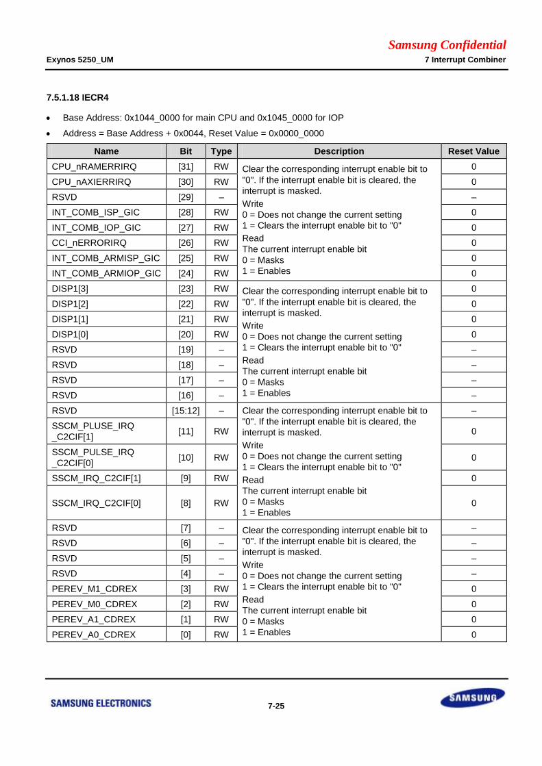
Samsung Confidential Exynos 5250_UM 7 Interrupt Combiner
7-25
7.5.1.18 IECR4
Base Address: 0x1044_0000 for main CPU and 0x1045_0000 for IOP
Address = Base Address + 0x0044, Reset Value = 0x0000_0000
Name Bit Type Description Reset Value
CPU_nRAMERRIRQ [31] RW Clear the corresponding interrupt enable bit to
"0". If the interrupt enable bit is cleared, the
interrupt is masked.
Write
0 = Does not change the current setting
1 = Clears the interrupt enable bit to "0"
Read
The current interrupt enable bit
0 = Masks
1 = Enables
0
CPU_nAXIERRIRQ [30] RW 0
RSVD [29] – –
INT_COMB_ISP_GIC [28] RW 0
INT_COMB_IOP_GIC [27] RW 0
CCI_nERRORIRQ [26] RW 0
INT_COMB_ARMISP_GIC [25] RW 0
INT_COMB_ARMIOP_GIC [24] RW 0
DISP1[3] [23] RW Clear the corresponding interrupt enable bit to
"0". If the interrupt enable bit is cleared, the
interrupt is masked.
Write
0 = Does not change the current setting
1 = Clears the interrupt enable bit to "0"
Read
The current interrupt enable bit
0 = Masks
1 = Enables
0
DISP1[2] [22] RW 0
DISP1[1] [21] RW 0
DISP1[0] [20] RW 0
RSVD [19] – –
RSVD [18] – –
RSVD [17] – –
RSVD [16] – –
RSVD [15:12] – Clear the corresponding interrupt enable bit to
"0". If the interrupt enable bit is cleared, the
interrupt is masked.
Write
0 = Does not change the current setting
1 = Clears the interrupt enable bit to "0"
Read
The current interrupt enable bit
0 = Masks
1 = Enables
–
SSCM_PLUSE_IRQ
_C2CIF[1] [11] RW 0
SSCM_PULSE_IRQ
_C2CIF[0] [10] RW 0
SSCM_IRQ_C2CIF[1] [9] RW 0
SSCM_IRQ_C2CIF[0] [8] RW 0
RSVD [7] – Clear the corresponding interrupt enable bit to
"0". If the interrupt enable bit is cleared, the
interrupt is masked.
Write
0 = Does not change the current setting
1 = Clears the interrupt enable bit to "0"
Read
The current interrupt enable bit
0 = Masks
1 = Enables
–
RSVD [6] – –
RSVD [5] – –
RSVD [4] – –
PEREV_M1_CDREX [3] RW 0
PEREV_M0_CDREX [2] RW 0
PEREV_A1_CDREX [1] RW 0
PEREV_A0_CDREX [0] RW 0
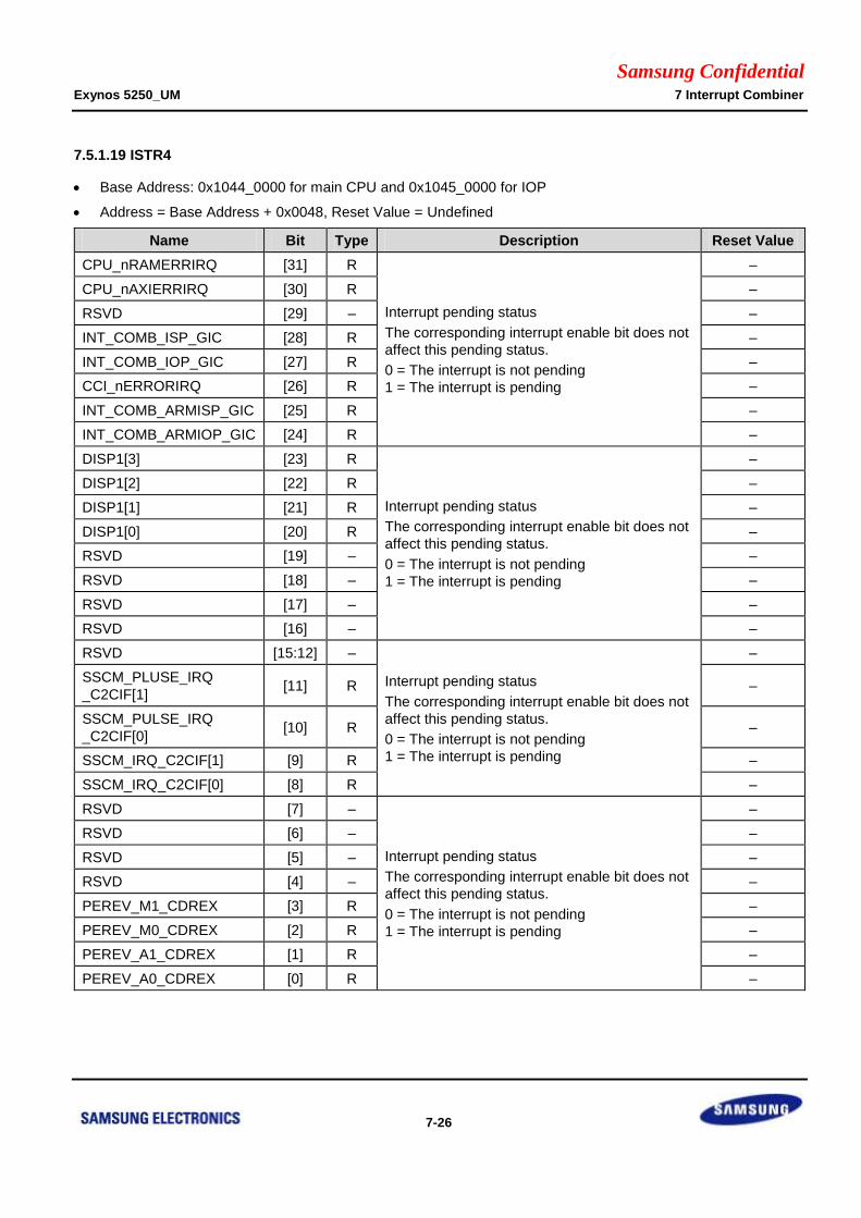
Samsung Confidential Exynos 5250_UM 7 Interrupt Combiner
7-26
7.5.1.19 ISTR4
Base Address: 0x1044_0000 for main CPU and 0x1045_0000 for IOP
Address = Base Address + 0x0048, Reset Value = Undefined
Name Bit Type Description Reset Value
CPU_nRAMERRIRQ [31] R
Interrupt pending status
The corresponding interrupt enable bit does not
affect this pending status.
0 = The interrupt is not pending
1 = The interrupt is pending
–
CPU_nAXIERRIRQ [30] R –
RSVD [29] – –
INT_COMB_ISP_GIC [28] R –
INT_COMB_IOP_GIC [27] R –
CCI_nERRORIRQ [26] R –
INT_COMB_ARMISP_GIC [25] R –
INT_COMB_ARMIOP_GIC [24] R –
DISP1[3] [23] R
Interrupt pending status
The corresponding interrupt enable bit does not
affect this pending status.
0 = The interrupt is not pending
1 = The interrupt is pending
–
DISP1[2] [22] R –
DISP1[1] [21] R –
DISP1[0] [20] R –
RSVD [19] – –
RSVD [18] – –
RSVD [17] – –
RSVD [16] – –
RSVD [15:12] –
Interrupt pending status
The corresponding interrupt enable bit does not
affect this pending status.
0 = The interrupt is not pending
1 = The interrupt is pending
–
SSCM_PLUSE_IRQ
_C2CIF[1] [11] R –
SSCM_PULSE_IRQ
_C2CIF[0] [10] R –
SSCM_IRQ_C2CIF[1] [9] R –
SSCM_IRQ_C2CIF[0] [8] R –
RSVD [7] –
Interrupt pending status
The corresponding interrupt enable bit does not
affect this pending status.
0 = The interrupt is not pending
1 = The interrupt is pending
–
RSVD [6] – –
RSVD [5] – –
RSVD [4] – –
PEREV_M1_CDREX [3] R –
PEREV_M0_CDREX [2] R –
PEREV_A1_CDREX [1] R –
PEREV_A0_CDREX [0] R –
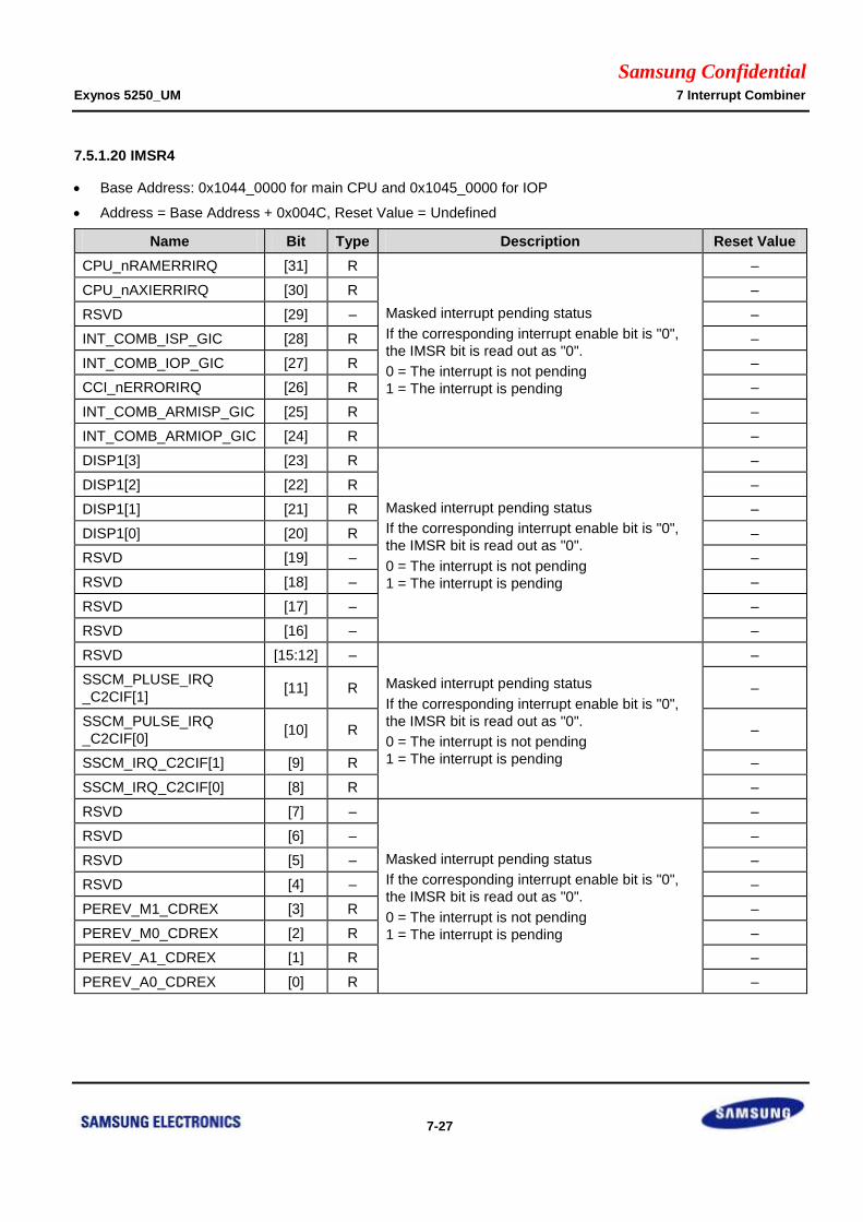
Samsung Confidential Exynos 5250_UM 7 Interrupt Combiner
7-27
7.5.1.20 IMSR4
Base Address: 0x1044_0000 for main CPU and 0x1045_0000 for IOP
Address = Base Address + 0x004C, Reset Value = Undefined
Name Bit Type Description Reset Value
CPU_nRAMERRIRQ [31] R
Masked interrupt pending status
If the corresponding interrupt enable bit is "0",
the IMSR bit is read out as "0".
0 = The interrupt is not pending
1 = The interrupt is pending
–
CPU_nAXIERRIRQ [30] R –
RSVD [29] – –
INT_COMB_ISP_GIC [28] R –
INT_COMB_IOP_GIC [27] R –
CCI_nERRORIRQ [26] R –
INT_COMB_ARMISP_GIC [25] R –
INT_COMB_ARMIOP_GIC [24] R –
DISP1[3] [23] R
Masked interrupt pending status
If the corresponding interrupt enable bit is "0",
the IMSR bit is read out as "0".
0 = The interrupt is not pending
1 = The interrupt is pending
–
DISP1[2] [22] R –
DISP1[1] [21] R –
DISP1[0] [20] R –
RSVD [19] – –
RSVD [18] – –
RSVD [17] – –
RSVD [16] – –
RSVD [15:12] –
Masked interrupt pending status
If the corresponding interrupt enable bit is "0",
the IMSR bit is read out as "0".
0 = The interrupt is not pending
1 = The interrupt is pending
–
SSCM_PLUSE_IRQ
_C2CIF[1] [11] R –
SSCM_PULSE_IRQ
_C2CIF[0] [10] R –
SSCM_IRQ_C2CIF[1] [9] R –
SSCM_IRQ_C2CIF[0] [8] R –
RSVD [7] –
Masked interrupt pending status
If the corresponding interrupt enable bit is "0",
the IMSR bit is read out as "0".
0 = The interrupt is not pending
1 = The interrupt is pending
–
RSVD [6] – –
RSVD [5] – –
RSVD [4] – –
PEREV_M1_CDREX [3] R –
PEREV_M0_CDREX [2] R –
PEREV_A1_CDREX [1] R –
PEREV_A0_CDREX [0] R –
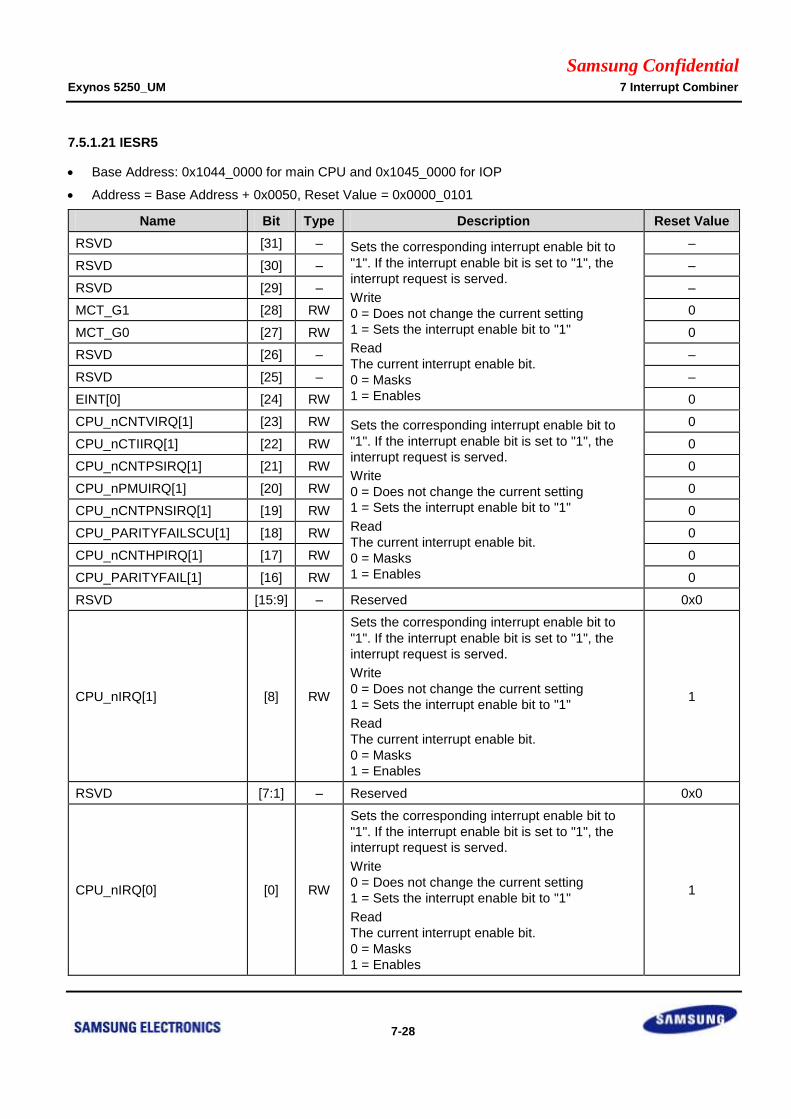
Samsung Confidential Exynos 5250_UM 7 Interrupt Combiner
7-28
7.5.1.21 IESR5
Base Address: 0x1044_0000 for main CPU and 0x1045_0000 for IOP
Address = Base Address + 0x0050, Reset Value = 0x0000_0101
Name Bit Type Description Reset Value
RSVD [31] – Sets the corresponding interrupt enable bit to
"1". If the interrupt enable bit is set to "1", the
interrupt request is served.
Write
0 = Does not change the current setting
1 = Sets the interrupt enable bit to "1"
Read
The current interrupt enable bit.
0 = Masks
1 = Enables
–
RSVD [30] – –
RSVD [29] – –
MCT_G1 [28] RW 0
MCT_G0 [27] RW 0
RSVD [26] – –
RSVD [25] – –
EINT[0] [24] RW 0
CPU_nCNTVIRQ[1] [23] RW Sets the corresponding interrupt enable bit to
"1". If the interrupt enable bit is set to "1", the
interrupt request is served.
Write
0 = Does not change the current setting
1 = Sets the interrupt enable bit to "1"
Read
The current interrupt enable bit.
0 = Masks
1 = Enables
0
CPU_nCTIIRQ[1] [22] RW 0
CPU_nCNTPSIRQ[1] [21] RW 0
CPU_nPMUIRQ[1] [20] RW 0
CPU_nCNTPNSIRQ[1] [19] RW 0
CPU_PARITYFAILSCU[1] [18] RW 0
CPU_nCNTHPIRQ[1] [17] RW 0
CPU_PARITYFAIL[1] [16] RW 0
RSVD [15:9] – Reserved 0x0
CPU_nIRQ[1] [8] RW
Sets the corresponding interrupt enable bit to
"1". If the interrupt enable bit is set to "1", the
interrupt request is served.
Write
0 = Does not change the current setting
1 = Sets the interrupt enable bit to "1"
Read
The current interrupt enable bit.
0 = Masks
1 = Enables
1
RSVD [7:1] – Reserved 0x0
CPU_nIRQ[0] [0] RW
Sets the corresponding interrupt enable bit to
"1". If the interrupt enable bit is set to "1", the
interrupt request is served.
Write
0 = Does not change the current setting
1 = Sets the interrupt enable bit to "1"
Read
The current interrupt enable bit.
0 = Masks
1 = Enables
1
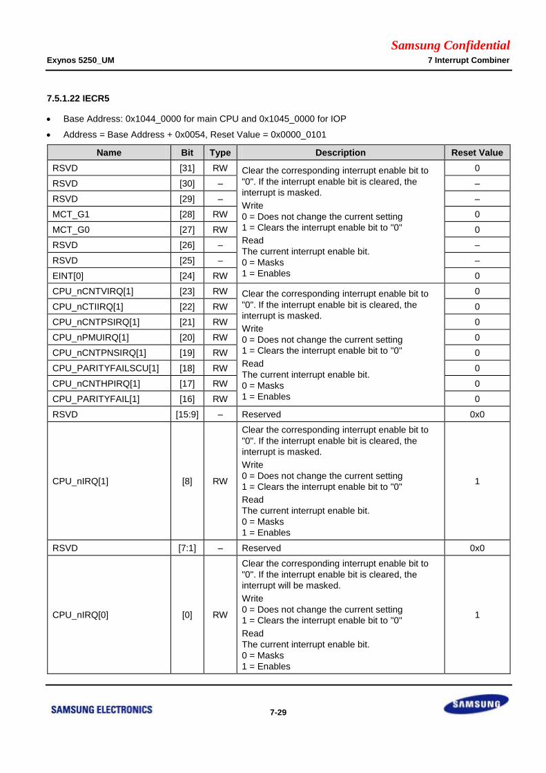
Samsung Confidential Exynos 5250_UM 7 Interrupt Combiner
7-29
7.5.1.22 IECR5
Base Address: 0x1044_0000 for main CPU and 0x1045_0000 for IOP
Address = Base Address + 0x0054, Reset Value = 0x0000_0101
Name Bit Type Description Reset Value
RSVD [31] RW Clear the corresponding interrupt enable bit to
"0". If the interrupt enable bit is cleared, the
interrupt is masked.
Write
0 = Does not change the current setting
1 = Clears the interrupt enable bit to "0"
Read
The current interrupt enable bit.
0 = Masks
1 = Enables
0
RSVD [30] – –
RSVD [29] – –
MCT_G1 [28] RW 0
MCT_G0 [27] RW 0
RSVD [26] – –
RSVD [25] – –
EINT[0] [24] RW 0
CPU_nCNTVIRQ[1] [23] RW Clear the corresponding interrupt enable bit to
"0". If the interrupt enable bit is cleared, the
interrupt is masked.
Write
0 = Does not change the current setting
1 = Clears the interrupt enable bit to "0"
Read
The current interrupt enable bit.
0 = Masks
1 = Enables
0
CPU_nCTIIRQ[1] [22] RW 0
CPU_nCNTPSIRQ[1] [21] RW 0
CPU_nPMUIRQ[1] [20] RW 0
CPU_nCNTPNSIRQ[1] [19] RW 0
CPU_PARITYFAILSCU[1] [18] RW 0
CPU_nCNTHPIRQ[1] [17] RW 0
CPU_PARITYFAIL[1] [16] RW 0
RSVD [15:9] – Reserved 0x0
CPU_nIRQ[1] [8] RW
Clear the corresponding interrupt enable bit to
"0". If the interrupt enable bit is cleared, the
interrupt is masked.
Write
0 = Does not change the current setting
1 = Clears the interrupt enable bit to "0"
Read
The current interrupt enable bit.
0 = Masks
1 = Enables
1
RSVD [7:1] – Reserved 0x0
CPU_nIRQ[0] [0] RW
Clear the corresponding interrupt enable bit to
"0". If the interrupt enable bit is cleared, the
interrupt will be masked.
Write
0 = Does not change the current setting
1 = Clears the interrupt enable bit to "0"
Read
The current interrupt enable bit.
0 = Masks
1 = Enables
1
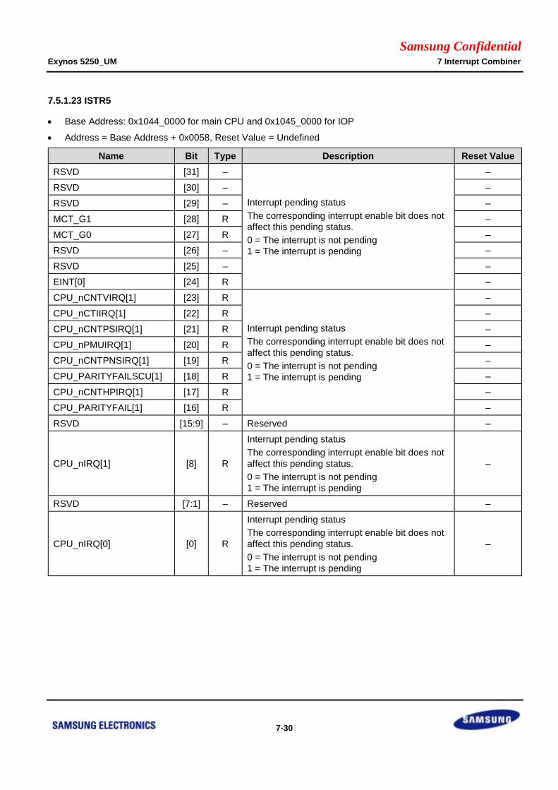
Samsung Confidential Exynos 5250_UM 7 Interrupt Combiner
7-30
7.5.1.23 ISTR5
Base Address: 0x1044_0000 for main CPU and 0x1045_0000 for IOP
Address = Base Address + 0x0058, Reset Value = Undefined
Name Bit Type Description Reset Value
RSVD [31] –
Interrupt pending status
The corresponding interrupt enable bit does not
affect this pending status.
0 = The interrupt is not pending
1 = The interrupt is pending
–
RSVD [30] – –
RSVD [29] – –
MCT_G1 [28] R –
MCT_G0 [27] R –
RSVD [26] – –
RSVD [25] – –
EINT[0] [24] R –
CPU_nCNTVIRQ[1] [23] R
Interrupt pending status
The corresponding interrupt enable bit does not
affect this pending status.
0 = The interrupt is not pending
1 = The interrupt is pending
–
CPU_nCTIIRQ[1] [22] R –
CPU_nCNTPSIRQ[1] [21] R –
CPU_nPMUIRQ[1] [20] R –
CPU_nCNTPNSIRQ[1] [19] R –
CPU_PARITYFAILSCU[1] [18] R –
CPU_nCNTHPIRQ[1] [17] R –
CPU_PARITYFAIL[1] [16] R –
RSVD [15:9] – Reserved –
CPU_nIRQ[1] [8] R
Interrupt pending status
The corresponding interrupt enable bit does not
affect this pending status.
0 = The interrupt is not pending
1 = The interrupt is pending
–
RSVD [7:1] – Reserved –
CPU_nIRQ[0] [0] R
Interrupt pending status
The corresponding interrupt enable bit does not
affect this pending status.
0 = The interrupt is not pending
1 = The interrupt is pending
–

Samsung Confidential Exynos 5250_UM 7 Interrupt Combiner
7-31
7.5.1.24 IMSR5
Base Address: 0x1044_0000 for main CPU and 0x1045_0000 for IOP
Address = Base Address + 0x005C, Reset Value = Undefined
Name Bit Type Description Reset Value
RSVD [31] –
Masked interrupt pending status
If the corresponding interrupt enable bit is "0",
the IMSR bit is read out as "0".
0 = The interrupt is not pending
1 = The interrupt is pending
–
RSVD [30] – –
RSVD [29] – –
MCT_G1 [28] R –
MCT_G0 [27] R –
RSVD [26] – –
RSVD [25] – –
EINT[0] [24] R –
CPU_nCNTVIRQ[1] [23] R
Masked interrupt pending status
If the corresponding interrupt enable bit is "0",
the IMSR bit is read out as "0".
0 = The interrupt is not pending
1 = The interrupt is pending
–
CPU_nCTIIRQ[1] [22] R –
CPU_nCNTPSIRQ[1] [21] R –
CPU_nPMUIRQ[1] [20] R –
CPU_nCNTPNSIRQ[1] [19] R –
CPU_PARITYFAILSCU[1] [18] R –
CPU_nCNTHPIRQ[1] [17] R –
CPU_PARITYFAIL[1] [16] R –
RSVD [15:9] – Reserved –
CPU_nIRQ[1] [8] R
Masked interrupt pending status
If the corresponding interrupt enable bit is "0",
the IMSR bit is read out as "0".
0 = The interrupt is not pending
1 = The interrupt is pending
–
RSVD [7:1] – Reserved –
CPU_nIRQ[0] [0] R
Masked interrupt pending status
If the corresponding interrupt enable bit is "0",
the IMSR bit is read out as "0".
0 = The interrupt is not pending
1 = The interrupt is pending
–
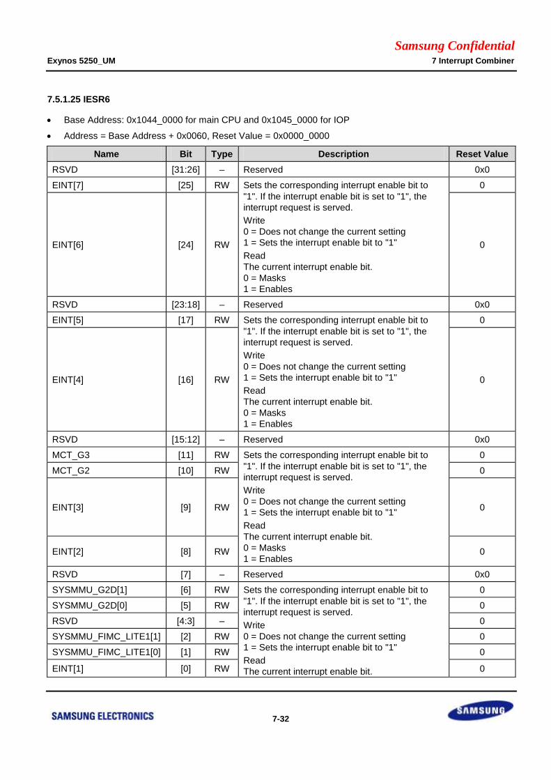
Samsung Confidential Exynos 5250_UM 7 Interrupt Combiner
7-32
7.5.1.25 IESR6
Base Address: 0x1044_0000 for main CPU and 0x1045_0000 for IOP
Address = Base Address + 0x0060, Reset Value = 0x0000_0000
Name Bit Type Description Reset Value
RSVD [31:26] – Reserved 0x0
EINT[7] [25] RW Sets the corresponding interrupt enable bit to
"1". If the interrupt enable bit is set to "1", the
interrupt request is served.
Write
0 = Does not change the current setting
1 = Sets the interrupt enable bit to "1"
Read
The current interrupt enable bit.
0 = Masks
1 = Enables
0
EINT[6] [24] RW 0
RSVD [23:18] – Reserved 0x0
EINT[5] [17] RW Sets the corresponding interrupt enable bit to
"1". If the interrupt enable bit is set to "1", the
interrupt request is served.
Write
0 = Does not change the current setting
1 = Sets the interrupt enable bit to "1"
Read
The current interrupt enable bit.
0 = Masks
1 = Enables
0
EINT[4] [16] RW 0
RSVD [15:12] – Reserved 0x0
MCT_G3 [11] RW Sets the corresponding interrupt enable bit to
"1". If the interrupt enable bit is set to "1", the
interrupt request is served.
Write
0 = Does not change the current setting
1 = Sets the interrupt enable bit to "1"
Read
The current interrupt enable bit.
0 = Masks
1 = Enables
0
MCT_G2 [10] RW 0
EINT[3] [9] RW 0
EINT[2] [8] RW 0
RSVD [7] – Reserved 0x0
SYSMMU_G2D[1] [6] RW Sets the corresponding interrupt enable bit to
"1". If the interrupt enable bit is set to "1", the
interrupt request is served.
Write
0 = Does not change the current setting
1 = Sets the interrupt enable bit to "1"
Read
The current interrupt enable bit.
0
SYSMMU_G2D[0] [5] RW 0
RSVD [4:3] – 0
SYSMMU_FIMC_LITE1[1] [2] RW 0
SYSMMU_FIMC_LITE1[0] [1] RW 0
EINT[1] [0] RW 0
Samsung Confidential Exynos 5250_UM 7 Interrupt Combiner
7-33
Name Bit Type Description Reset Value
0 = Masks
1 = Enables
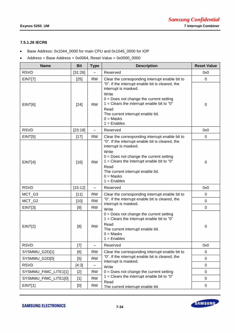
Samsung Confidential Exynos 5250_UM 7 Interrupt Combiner
7-34
7.5.1.26 IECR6
Base Address: 0x1044_0000 for main CPU and 0x1045_0000 for IOP
Address = Base Address + 0x0064, Reset Value = 0x0000_0000
Name Bit Type Description Reset Value
RSVD [31:26] – Reserved 0x0
EINT[7] [25] RW Clear the corresponding interrupt enable bit to
"0". If the interrupt enable bit is cleared, the
interrupt is masked.
Write
0 = Does not change the current setting
1 = Clears the interrupt enable bit to "0"
Read
The current interrupt enable bit.
0 = Masks
1 = Enables
0
EINT[6] [24] RW 0
RSVD [23:18] – Reserved 0x0
EINT[5] [17] RW Clear the corresponding interrupt enable bit to
"0". If the interrupt enable bit is cleared, the
interrupt is masked.
Write
0 = Does not change the current setting
1 = Clears the interrupt enable bit to "0"
Read
The current interrupt enable bit.
0 = Masks
1 = Enables
0
EINT[4] [16] RW 0
RSVD [15:12] – Reserved 0x0
MCT_G3 [11] RW Clear the corresponding interrupt enable bit to
"0". If the interrupt enable bit is cleared, the
interrupt is masked.
Write
0 = Does not change the current setting
1 = Clears the interrupt enable bit to "0"
Read
The current interrupt enable bit.
0 = Masks
1 = Enables
0
MCT_G2 [10] RW 0
EINT[3] [9] RW 0
EINT[2] [8] RW 0
RSVD [7] – Reserved 0x0
SYSMMU_G2D[1] [6] RW Clear the corresponding interrupt enable bit to
"0". If the interrupt enable bit is cleared, the
interrupt is masked.
Write
0 = Does not change the current setting
1 = Clears the interrupt enable bit to "0"
Read
The current interrupt enable bit.
0
SYSMMU_G2D[0] [5] RW 0
RSVD [4:3] – 0
SYSMMU_FIMC_LITE1[1] [2] RW 0
SYSMMU_FIMC_LITE1[0] [1] RW 0
EINT[1] [0] RW 0

Samsung Confidential Exynos 5250_UM 7 Interrupt Combiner
7-35
Name Bit Type Description Reset Value
0 = Masks
1 = Enables
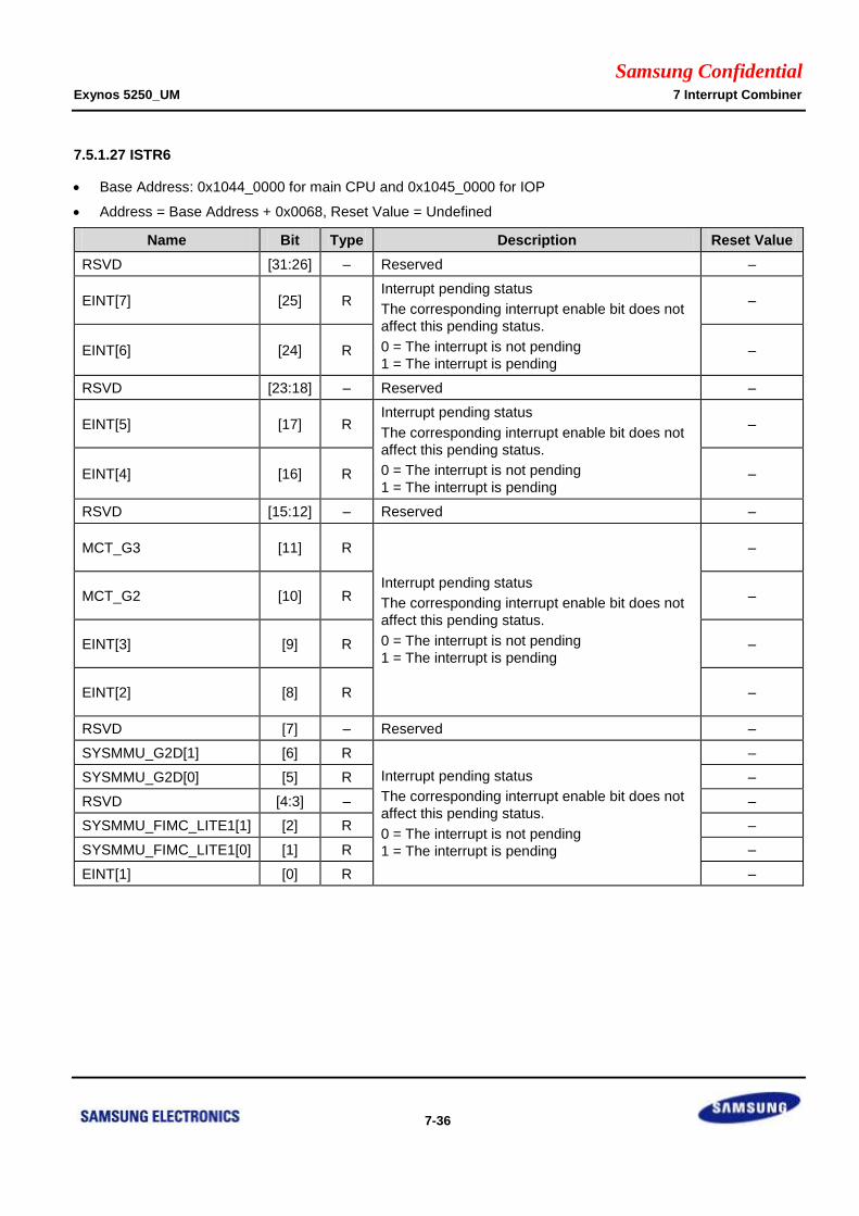
Samsung Confidential Exynos 5250_UM 7 Interrupt Combiner
7-36
7.5.1.27 ISTR6
Base Address: 0x1044_0000 for main CPU and 0x1045_0000 for IOP
Address = Base Address + 0x0068, Reset Value = Undefined
Name Bit Type Description Reset Value
RSVD [31:26] – Reserved –
EINT[7] [25] R Interrupt pending status
The corresponding interrupt enable bit does not
affect this pending status.
0 = The interrupt is not pending
1 = The interrupt is pending
–
EINT[6] [24] R –
RSVD [23:18] – Reserved –
EINT[5] [17] R Interrupt pending status
The corresponding interrupt enable bit does not
affect this pending status.
0 = The interrupt is not pending
1 = The interrupt is pending
–
EINT[4] [16] R –
RSVD [15:12] – Reserved –
MCT_G3 [11] R
Interrupt pending status
The corresponding interrupt enable bit does not
affect this pending status.
0 = The interrupt is not pending
1 = The interrupt is pending
–
MCT_G2 [10] R –
EINT[3] [9] R –
EINT[2] [8] R –
RSVD [7] – Reserved –
SYSMMU_G2D[1] [6] R
Interrupt pending status
The corresponding interrupt enable bit does not
affect this pending status.
0 = The interrupt is not pending
1 = The interrupt is pending
–
SYSMMU_G2D[0] [5] R –
RSVD [4:3] – –
SYSMMU_FIMC_LITE1[1] [2] R –
SYSMMU_FIMC_LITE1[0] [1] R –
EINT[1] [0] R –
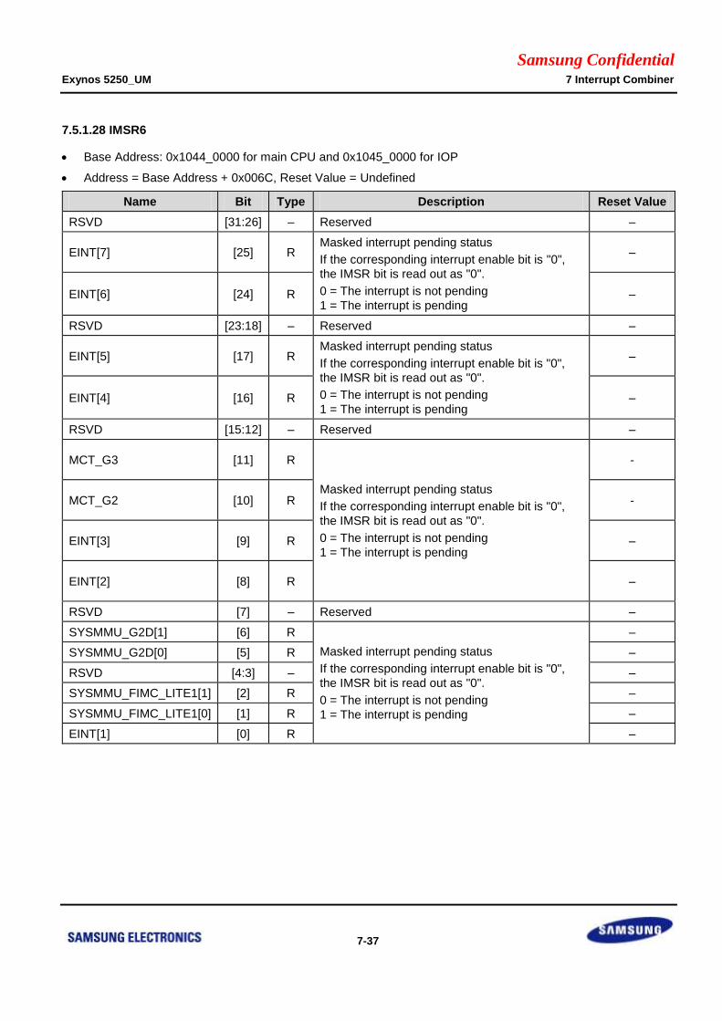
Samsung Confidential Exynos 5250_UM 7 Interrupt Combiner
7-37
7.5.1.28 IMSR6
Base Address: 0x1044_0000 for main CPU and 0x1045_0000 for IOP
Address = Base Address + 0x006C, Reset Value = Undefined
Name Bit Type Description Reset Value
RSVD [31:26] – Reserved –
EINT[7] [25] R Masked interrupt pending status
If the corresponding interrupt enable bit is "0",
the IMSR bit is read out as "0".
0 = The interrupt is not pending
1 = The interrupt is pending
–
EINT[6] [24] R –
RSVD [23:18] – Reserved –
EINT[5] [17] R Masked interrupt pending status
If the corresponding interrupt enable bit is "0",
the IMSR bit is read out as "0".
0 = The interrupt is not pending
1 = The interrupt is pending
–
EINT[4] [16] R –
RSVD [15:12] – Reserved –
MCT_G3 [11] R
Masked interrupt pending status
If the corresponding interrupt enable bit is "0",
the IMSR bit is read out as "0".
0 = The interrupt is not pending
1 = The interrupt is pending
-
MCT_G2 [10] R -
EINT[3] [9] R –
EINT[2] [8] R –
RSVD [7] – Reserved –
SYSMMU_G2D[1] [6] R
Masked interrupt pending status
If the corresponding interrupt enable bit is "0",
the IMSR bit is read out as "0".
0 = The interrupt is not pending
1 = The interrupt is pending
–
SYSMMU_G2D[0] [5] R –
RSVD [4:3] – –
SYSMMU_FIMC_LITE1[1] [2] R –
SYSMMU_FIMC_LITE1[0] [1] R –
EINT[1] [0] R –
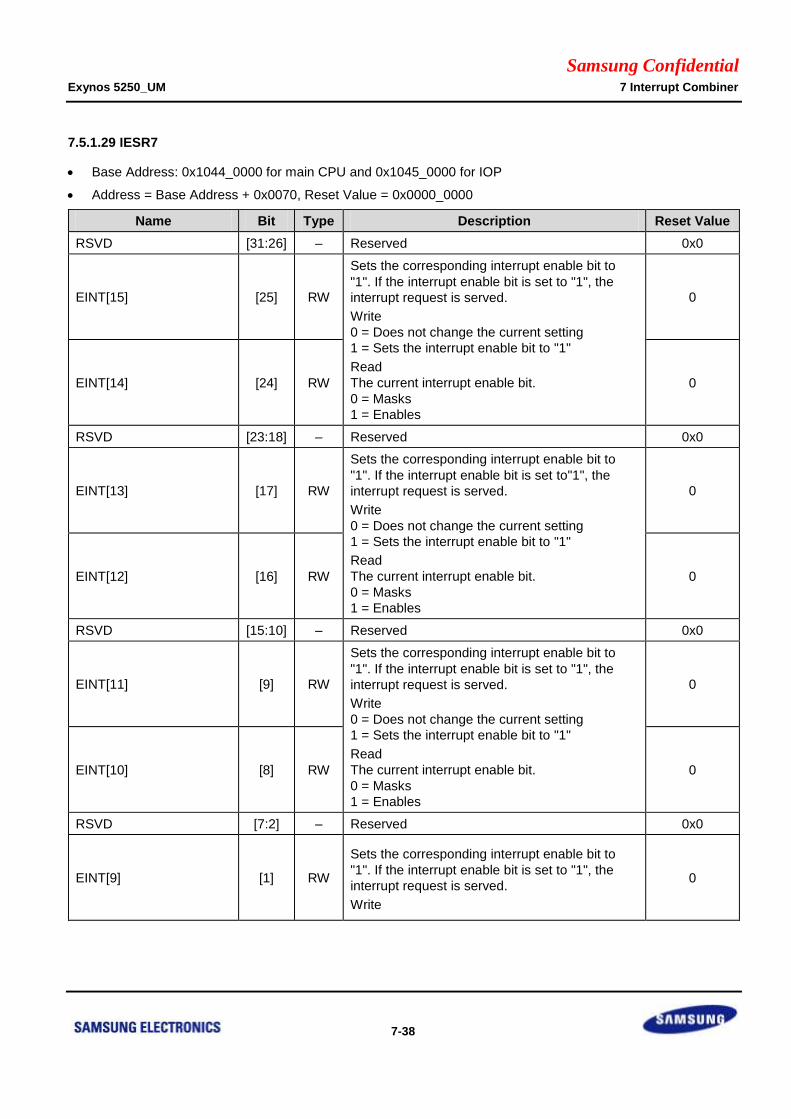
Samsung Confidential Exynos 5250_UM 7 Interrupt Combiner
7-38
7.5.1.29 IESR7
Base Address: 0x1044_0000 for main CPU and 0x1045_0000 for IOP
Address = Base Address + 0x0070, Reset Value = 0x0000_0000
Name Bit Type Description Reset Value
RSVD [31:26] – Reserved 0x0
EINT[15] [25] RW
Sets the corresponding interrupt enable bit to
"1". If the interrupt enable bit is set to "1", the
interrupt request is served.
Write
0 = Does not change the current setting
1 = Sets the interrupt enable bit to "1"
Read
The current interrupt enable bit.
0 = Masks
1 = Enables
0
EINT[14] [24] RW 0
RSVD [23:18] – Reserved 0x0
EINT[13] [17] RW
Sets the corresponding interrupt enable bit to
"1". If the interrupt enable bit is set to"1", the
interrupt request is served.
Write
0 = Does not change the current setting
1 = Sets the interrupt enable bit to "1"
Read
The current interrupt enable bit.
0 = Masks
1 = Enables
0
EINT[12] [16] RW 0
RSVD [15:10] – Reserved 0x0
EINT[11] [9] RW
Sets the corresponding interrupt enable bit to
"1". If the interrupt enable bit is set to "1", the
interrupt request is served.
Write
0 = Does not change the current setting
1 = Sets the interrupt enable bit to "1"
Read
The current interrupt enable bit.
0 = Masks
1 = Enables
0
EINT[10] [8] RW 0
RSVD [7:2] – Reserved 0x0
EINT[9] [1] RW
Sets the corresponding interrupt enable bit to
"1". If the interrupt enable bit is set to "1", the
interrupt request is served.
Write
0

Samsung Confidential Exynos 5250_UM 7 Interrupt Combiner
7-39
Name Bit Type Description Reset Value
EINT[8] [0] RW
0 = Does not change the current setting
1 = Sets the interrupt enable bit to "1"
Read
The current interrupt enable bit.
0 = Masks
1 = Enables
0

Samsung Confidential Exynos 5250_UM 7 Interrupt Combiner
7-40
7.5.1.30 IECR7
Base Address: 0x1044_0000 for main CPU and 0x1045_0000 for IOP
Address = Base Address + 0x0074, Reset Value = 0x0000_0000
Name Bit Type Description Reset Value
RSVD [31:26] – Reserved 0x0
EINT[15] [25] RW
Clear the corresponding interrupt enable bit to
"0". If the interrupt enable bit is cleared, the
interrupt is masked.
Write
0 = Does not change the current setting
1 = Clears the interrupt enable bit to "0"
Read
The current interrupt enable bit.
0 = Masks
1 = Enables
0
EINT[14] [24] RW 0
RSVD [23:18] – Reserved 0x0
EINT[13] [17] RW
Clear the corresponding interrupt enable bit to
"0". If the interrupt enable bit is cleared, the
interrupt is masked.
Write
0 = Does not change the current setting
1 = Clears the interrupt enable bit to "0"
Read
The current interrupt enable bit.
0 = Masks
1 = Enables
0
EINT[12] [16] RW 0
RSVD [15:10] – Reserved 0x0
EINT[11] [9] RW
Clear the corresponding interrupt enable bit to
"0". If the interrupt enable bit is cleared, the
interrupt is masked.
Write
0 = Does not change the current setting
1 = Clears the interrupt enable bit to "0"
Read
The current interrupt enable bit.
0 = Masks
1 = Enables
0
EINT[10] [8] RW 0
RSVD [7:2] – Reserved 0x0
EINT[9] [1] RW
Clear the corresponding interrupt enable bit to
"0". If the interrupt enable bit is cleared, the
interrupt is masked.
Write
0
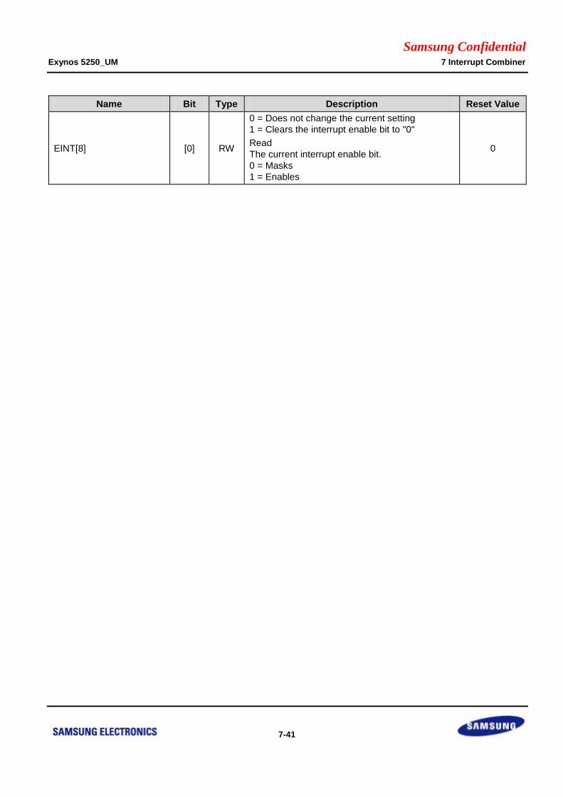
Samsung Confidential Exynos 5250_UM 7 Interrupt Combiner
7-41
Name Bit Type Description Reset Value
EINT[8] [0] RW
0 = Does not change the current setting
1 = Clears the interrupt enable bit to "0"
Read
The current interrupt enable bit.
0 = Masks
1 = Enables
0

Samsung Confidential Exynos 5250_UM 7 Interrupt Combiner
7-42
7.5.1.31 ISTR7
Base Address: 0x1044_0000 for main CPU and 0x1045_0000 for IOP
Address = Base Address + 0x0078, Reset Value = Undefined
Name Bit Type Description Reset Value
RSVD [31:26] – Reserved –
EINT[15] [25] R Interrupt pending status
The corresponding interrupt enable bit does not
affect this pending status.
0 = The interrupt is not pending
1 = The interrupt is pending
–
EINT[14] [24] R –
RSVD [23:18] – Reserved –
EINT[13] [17] R Interrupt pending status
The corresponding interrupt enable bit does not
affect this pending status.
0 = The interrupt is not pending
1 = The interrupt is pending
–
EINT[12] [16] R –
RSVD [15:10] – Reserved –
EINT[11] [9] R Interrupt pending status
The corresponding interrupt enable bit does not
affect this pending status.
0 = The interrupt is not pending
1 = The interrupt is pending
–
EINT[10] [8] R –
RSVD [7:2] – Reserved –
EINT[9] [1] R Interrupt pending status
The corresponding interrupt enable bit does not
affect this pending status.
0 = The interrupt is not pending
1 = The interrupt is pending
–
EINT[8] [0] R –
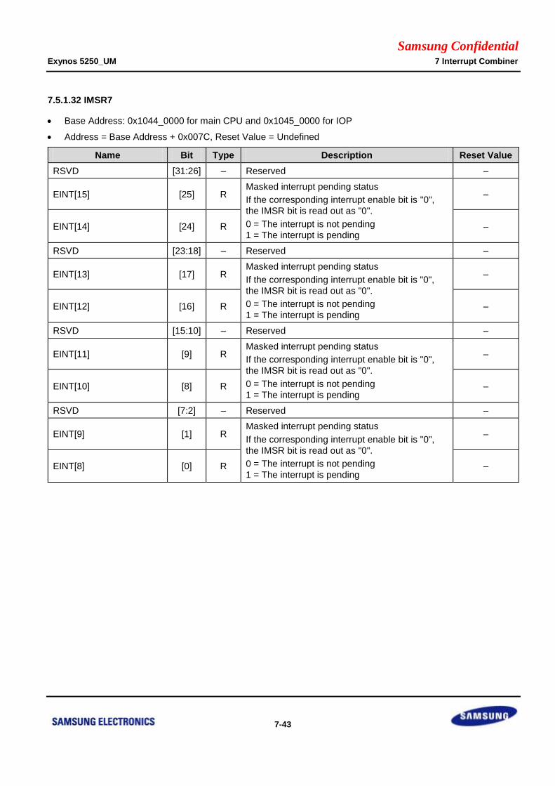
Samsung Confidential Exynos 5250_UM 7 Interrupt Combiner
7-43
7.5.1.32 IMSR7
Base Address: 0x1044_0000 for main CPU and 0x1045_0000 for IOP
Address = Base Address + 0x007C, Reset Value = Undefined
Name Bit Type Description Reset Value
RSVD [31:26] – Reserved –
EINT[15] [25] R Masked interrupt pending status
If the corresponding interrupt enable bit is "0",
the IMSR bit is read out as "0".
0 = The interrupt is not pending
1 = The interrupt is pending
–
EINT[14] [24] R –
RSVD [23:18] – Reserved –
EINT[13] [17] R Masked interrupt pending status
If the corresponding interrupt enable bit is "0",
the IMSR bit is read out as "0".
0 = The interrupt is not pending
1 = The interrupt is pending
–
EINT[12] [16] R –
RSVD [15:10] – Reserved –
EINT[11] [9] R Masked interrupt pending status
If the corresponding interrupt enable bit is "0",
the IMSR bit is read out as "0".
0 = The interrupt is not pending
1 = The interrupt is pending
–
EINT[10] [8] R –
RSVD [7:2] – Reserved –
EINT[9] [1] R Masked interrupt pending status
If the corresponding interrupt enable bit is "0",
the IMSR bit is read out as "0".
0 = The interrupt is not pending
1 = The interrupt is pending
–
EINT[8] [0] R –

Samsung Confidential Exynos 5250_UM 7 Interrupt Combiner
7-44
7.5.1.33 CIPSR0
Base Address: 0x1044_0000 for main CPU and 0x1045_0000 for IOP
Address = Base Address + 0x0100, Reset Value = Undefined
Name Bit Type Description Reset Value
INTG31 [31] R
Combined interrupt pending status
0 = The combined interrupt is not pending.
1 = The combined interrupt is pending. This
indicates that the corresponding interrupt request
to the GIC is asserted.
–
INTG30 [30] R –
INTG29 [29] R –
INTG28 [28] R –
INTG27 [27] R –
INTG26 [26] R –
INTG25 [25] R –
INTG24 [24] R –
INTG23 [23] R –
INTG22 [22] R –
INTG21 [21] R –
INTG20 [20] R –
INTG19 [19] R –
INTG18 [18] R –
INTG17 [17] R –
INTG16 [16] R –
INTG15 [15] R –
INTG14 [14] R –
INTG13 [13] R –
INTG12 [12] R –
INTG11 [11] R –
INTG10 [10] R –
INTG9 [9] R –
INTG8 [8] R –
INTG7 [7] R –
INTG6 [6] R –
INTG5 [5] R –
INTG4 [4] R –
INTG3 [3] R –
INTG2 [2] R –
INTG1 [1] R –
INTG0 [0] R –

Samsung Confidential Exynos 5250_UM 8 DMA (Direct Memory Access) Controller
8-1
8 DMA (Direct Memory Access) Controller
8.1 Overview
Exynos 5250 has three DMA controller:
Two DMA controller transfers from Memory to Memory. (MDMA0, MDMA1)
One DMA controller transfers Peripheral-to-Memory and vice-versa. (PDMA)
The MDMA Controller consists of one DMA330 and a few logics. The PDMA Controller consists of two DMA330
(PDMA0 and PDMA1) and dma_mapper.
Figure 8-1 illustrates the two type of DMA controller.
PDMA0 (DMA330r1p1) PDMA1 (DMA330r1p1)
dma_mapper
REQ from IPs
IRQ to
Interrupt Controller
IRQ to
Interrupt Controller
PDMA
MDMA0 (DMA330r1p1)
IRQ to
Interrupt Controller
MDMA1 (DMA330r1p1)
IRQ to
Interrupt Controller
Figure 8-1 Two type of DMA Controller
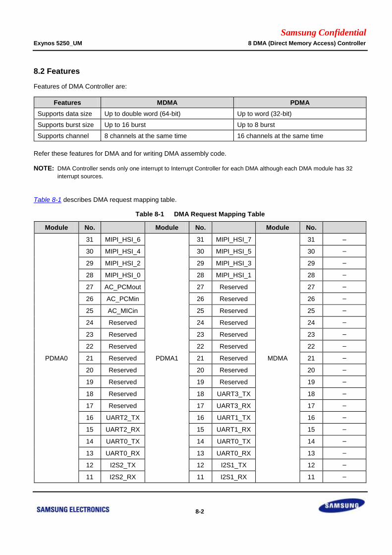
Samsung Confidential Exynos 5250_UM 8 DMA (Direct Memory Access) Controller
8-2
8.2 Features
Features of DMA Controller are:
Features MDMA PDMA
Supports data size Up to double word (64-bit) Up to word (32-bit)
Supports burst size Up to 16 burst Up to 8 burst
Supports channel 8 channels at the same time 16 channels at the same time
Refer these features for DMA and for writing DMA assembly code.
NOTE: DMA Controller sends only one interrupt to Interrupt Controller for each DMA although each DMA module has 32
interrupt sources.
Table 8-1 describes DMA request mapping table.
Table 8-1 DMA Request Mapping Table
Module No.
Module No.
Module No.
PDMA0
31 MIPI_HSI_6
PDMA1
31 MIPI_HSI_7
MDMA
31 –
30 MIPI_HSI_4 30 MIPI_HSI_5 30 –
29 MIPI_HSI_2 29 MIPI_HSI_3 29 –
28 MIPI_HSI_0 28 MIPI_HSI_1 28 –
27 AC_PCMout 27 Reserved 27 –
26 AC_PCMin 26 Reserved 26 –
25 AC_MICin 25 Reserved 25 –
24 Reserved 24 Reserved 24 –
23 Reserved 23 Reserved 23 –
22 Reserved 22 Reserved 22 –
21 Reserved 21 Reserved 21 –
20 Reserved 20 Reserved 20 –
19 Reserved 19 Reserved 19 –
18 Reserved 18 UART3_TX 18 –
17 Reserved 17 UART3_RX 17 –
16 UART2_TX 16 UART1_TX 16 –
15 UART2_RX 15 UART1_RX 15 –
14 UART0_TX 14 UART0_TX 14 –
13 UART0_RX 13 UART0_RX 13 –
12 I2S2_TX 12 I2S1_TX 12 –
11 I2S2_RX 11 I2S1_RX 11 –
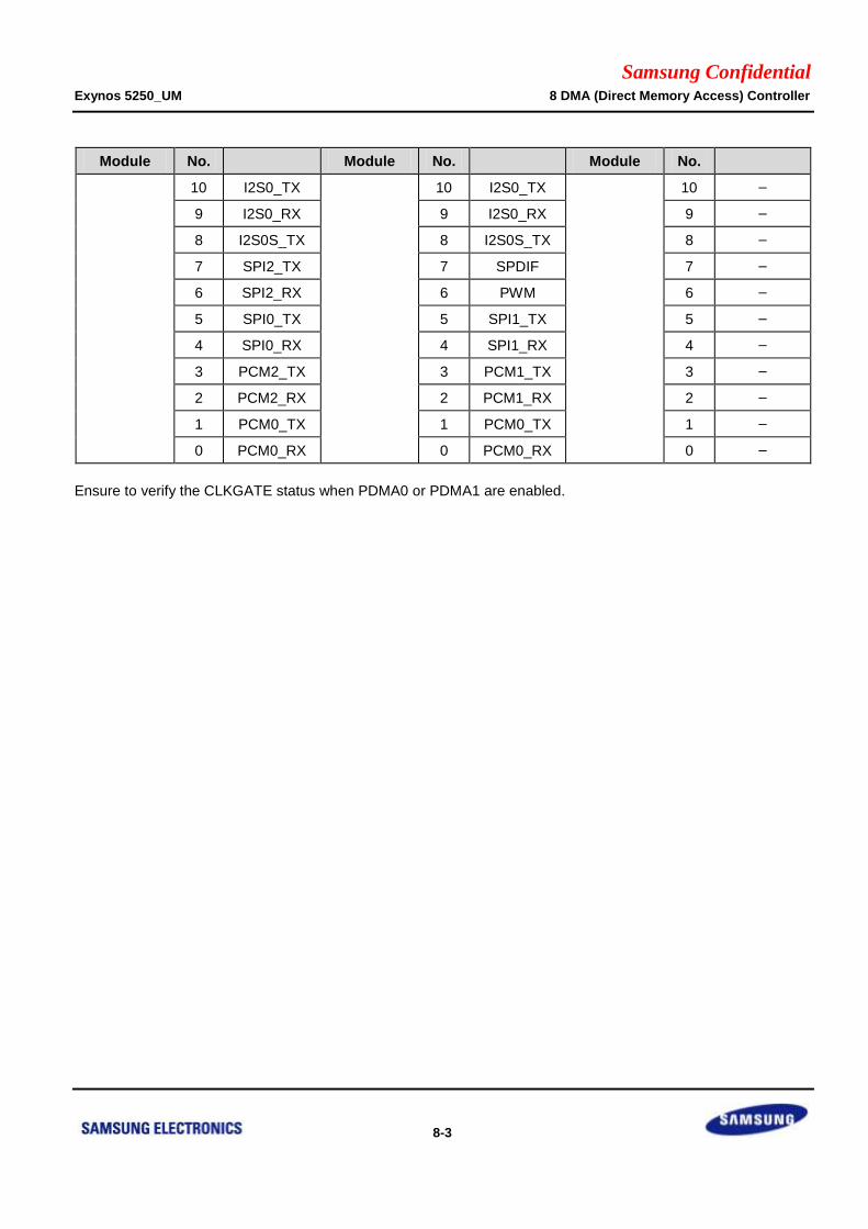
Samsung Confidential Exynos 5250_UM 8 DMA (Direct Memory Access) Controller
8-3
Module No.
Module No.
Module No.
10 I2S0_TX 10 I2S0_TX 10 –
9 I2S0_RX 9 I2S0_RX 9 –
8 I2S0S_TX 8 I2S0S_TX 8 –
7 SPI2_TX 7 SPDIF 7 –
6 SPI2_RX 6 PWM 6 –
5 SPI0_TX 5 SPI1_TX 5 –
4 SPI0_RX 4 SPI1_RX 4 –
3 PCM2_TX 3 PCM1_TX 3 –
2 PCM2_RX 2 PCM1_RX 2 –
1 PCM0_TX 1 PCM0_TX 1 –
0 PCM0_RX 0 PCM0_RX 0 –
Ensure to verify the CLKGATE status when PDMA0 or PDMA1 are enabled.
Samsung Confidential Exynos 5250_UM 8 DMA (Direct Memory Access) Controller
8-4
8.3 Functional Description
8.3.1 Instruction
Please refer to the PL330 TRM, "AMBA DMA Controller DMA-330 technical reference manual revision r1p1" from
ARM®.
8.3.1.1 Security Scheme
MDMA controller and PDMA controller run in the non-secure mode only.
8.3.1.2 Summary
Configuring DMAC:
You can configure DMAC with up to eight DMA channels. Each channel is capable of supporting a single
concurrent thread of DMA operation. Additionally, there is a single DMA manager thread to initialize the DMA
channel thread.
Channel thread:
Each channel thread can operate DMA. Ensure to write the assembly code accordingly. When you require a
number of independent DMA channels, you must write a number of assembly codes for each channel.
Assemble these channels, link them into one file, and load this file into memory.
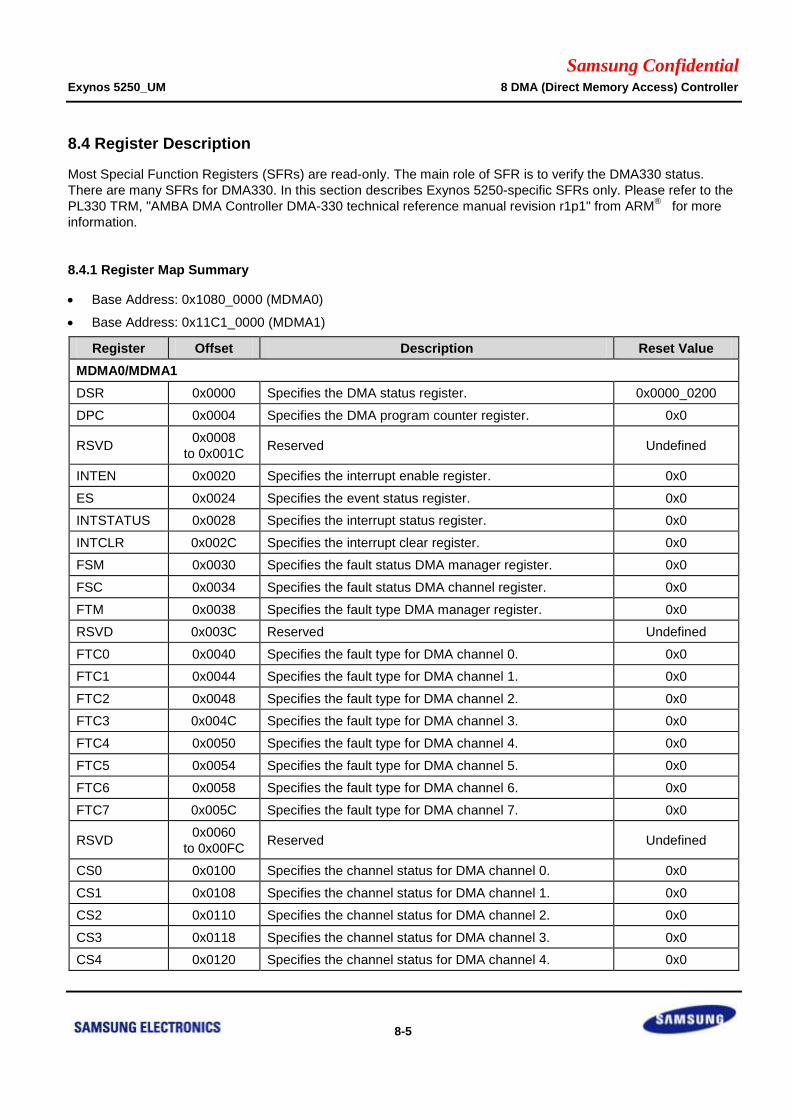
Samsung Confidential Exynos 5250_UM 8 DMA (Direct Memory Access) Controller
8-5
8.4 Register Description
Most Special Function Registers (SFRs) are read-only. The main role of SFR is to verify the DMA330 status.
There are many SFRs for DMA330. In this section describes Exynos 5250-specific SFRs only. Please refer to the
PL330 TRM, "AMBA DMA Controller DMA-330 technical reference manual revision r1p1" from ARM®
for more
information.
8.4.1 Register Map Summary
Base Address: 0x1080_0000 (MDMA0)
Base Address: 0x11C1_0000 (MDMA1)
Register Offset Description Reset Value
MDMA0/MDMA1
DSR 0x0000 Specifies the DMA status register. 0x0000_0200
DPC 0x0004 Specifies the DMA program counter register. 0x0
RSVD 0x0008
to 0x001C Reserved Undefined
INTEN 0x0020 Specifies the interrupt enable register. 0x0
ES 0x0024 Specifies the event status register. 0x0
INTSTATUS 0x0028 Specifies the interrupt status register. 0x0
INTCLR 0x002C Specifies the interrupt clear register. 0x0
FSM 0x0030 Specifies the fault status DMA manager register. 0x0
FSC 0x0034 Specifies the fault status DMA channel register. 0x0
FTM 0x0038 Specifies the fault type DMA manager register. 0x0
RSVD 0x003C Reserved Undefined
FTC0 0x0040 Specifies the fault type for DMA channel 0. 0x0
FTC1 0x0044 Specifies the fault type for DMA channel 1. 0x0
FTC2 0x0048 Specifies the fault type for DMA channel 2. 0x0
FTC3 0x004C Specifies the fault type for DMA channel 3. 0x0
FTC4 0x0050 Specifies the fault type for DMA channel 4. 0x0
FTC5 0x0054 Specifies the fault type for DMA channel 5. 0x0
FTC6 0x0058 Specifies the fault type for DMA channel 6. 0x0
FTC7 0x005C Specifies the fault type for DMA channel 7. 0x0
RSVD 0x0060
to 0x00FC Reserved Undefined
CS0 0x0100 Specifies the channel status for DMA channel 0. 0x0
CS1 0x0108 Specifies the channel status for DMA channel 1. 0x0
CS2 0x0110 Specifies the channel status for DMA channel 2. 0x0
CS3 0x0118 Specifies the channel status for DMA channel 3. 0x0
CS4 0x0120 Specifies the channel status for DMA channel 4. 0x0
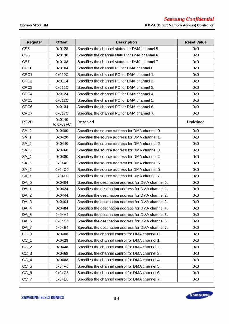
Samsung Confidential Exynos 5250_UM 8 DMA (Direct Memory Access) Controller
8-6
Register Offset Description Reset Value
CS5 0x0128 Specifies the channel status for DMA channel 5. 0x0
CS6 0x0130 Specifies the channel status for DMA channel 6. 0x0
CS7 0x0138 Specifies the channel status for DMA channel 7. 0x0
CPC0 0x0104 Specifies the channel PC for DMA channel 0. 0x0
CPC1 0x010C Specifies the channel PC for DMA channel 1. 0x0
CPC2 0x0114 Specifies the channel PC for DMA channel 2. 0x0
CPC3 0x011C Specifies the channel PC for DMA channel 3. 0x0
CPC4 0x0124 Specifies the channel PC for DMA channel 4. 0x0
CPC5 0x012C Specifies the channel PC for DMA channel 5. 0x0
CPC6 0x0134 Specifies the channel PC for DMA channel 6. 0x0
CPC7 0x013C Specifies the channel PC for DMA channel 7. 0x0
RSVD 0x0140
to 0x03FC Reserved Undefined
SA_0 0x0400 Specifies the source address for DMA channel 0. 0x0
SA_1 0x0420 Specifies the source address for DMA channel 1. 0x0
SA_2 0x0440 Specifies the source address for DMA channel 2. 0x0
SA_3 0x0460 Specifies the source address for DMA channel 3. 0x0
SA_4 0x0480 Specifies the source address for DMA channel 4. 0x0
SA_5 0x04A0 Specifies the source address for DMA channel 5. 0x0
SA_6 0x04C0 Specifies the source address for DMA channel 6. 0x0
SA_7 0x04E0 Specifies the source address for DMA channel 7. 0x0
DA_0 0x0404 Specifies the destination address for DMA channel 0. 0x0
DA_1 0x0424 Specifies the destination address for DMA channel 1. 0x0
DA_2 0x0444 Specifies the destination address for DMA channel 2. 0x0
DA_3 0x0464 Specifies the destination address for DMA channel 3. 0x0
DA_4 0x0484 Specifies the destination address for DMA channel 4. 0x0
DA_5 0x04A4 Specifies the destination address for DMA channel 5. 0x0
DA_6 0x04C4 Specifies the destination address for DMA channel 6. 0x0
DA_7 0x04E4 Specifies the destination address for DMA channel 7. 0x0
CC_0 0x0408 Specifies the channel control for DMA channel 0. 0x0
CC_1 0x0428 Specifies the channel control for DMA channel 1. 0x0
CC_2 0x0448 Specifies the channel control for DMA channel 2. 0x0
CC_3 0x0468 Specifies the channel control for DMA channel 3. 0x0
CC_4 0x0488 Specifies the channel control for DMA channel 4. 0x0
CC_5 0x04A8 Specifies the channel control for DMA channel 5. 0x0
CC_6 0x04C8 Specifies the channel control for DMA channel 6. 0x0
CC_7 0x04E8 Specifies the channel control for DMA channel 7. 0x0
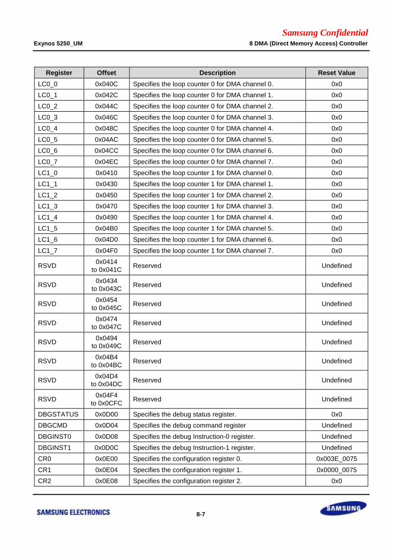
Samsung Confidential Exynos 5250_UM 8 DMA (Direct Memory Access) Controller
8-7
Register Offset Description Reset Value
LC0_0 0x040C Specifies the loop counter 0 for DMA channel 0. 0x0
LC0_1 0x042C Specifies the loop counter 0 for DMA channel 1. 0x0
LC0_2 0x044C Specifies the loop counter 0 for DMA channel 2. 0x0
LC0_3 0x046C Specifies the loop counter 0 for DMA channel 3. 0x0
LC0_4 0x048C Specifies the loop counter 0 for DMA channel 4. 0x0
LC0_5 0x04AC Specifies the loop counter 0 for DMA channel 5. 0x0
LC0_6 0x04CC Specifies the loop counter 0 for DMA channel 6. 0x0
LC0_7 0x04EC Specifies the loop counter 0 for DMA channel 7. 0x0
LC1_0 0x0410 Specifies the loop counter 1 for DMA channel 0. 0x0
LC1_1 0x0430 Specifies the loop counter 1 for DMA channel 1. 0x0
LC1_2 0x0450 Specifies the loop counter 1 for DMA channel 2. 0x0
LC1_3 0x0470 Specifies the loop counter 1 for DMA channel 3. 0x0
LC1_4 0x0490 Specifies the loop counter 1 for DMA channel 4. 0x0
LC1_5 0x04B0 Specifies the loop counter 1 for DMA channel 5. 0x0
LC1_6 0x04D0 Specifies the loop counter 1 for DMA channel 6. 0x0
LC1_7 0x04F0 Specifies the loop counter 1 for DMA channel 7. 0x0
RSVD 0x0414
to 0x041C Reserved Undefined
RSVD 0x0434
to 0x043C Reserved Undefined
RSVD 0x0454
to 0x045C Reserved Undefined
RSVD 0x0474
to 0x047C Reserved Undefined
RSVD 0x0494
to 0x049C Reserved Undefined
RSVD 0x04B4
to 0x04BC Reserved Undefined
RSVD 0x04D4
to 0x04DC Reserved Undefined
RSVD 0x04F4
to 0x0CFC Reserved Undefined
DBGSTATUS 0x0D00 Specifies the debug status register. 0x0
DBGCMD 0x0D04 Specifies the debug command register Undefined
DBGINST0 0x0D08 Specifies the debug Instruction-0 register. Undefined
DBGINST1 0x0D0C Specifies the debug Instruction-1 register. Undefined
CR0 0x0E00 Specifies the configuration register 0. 0x003E_0075
CR1 0x0E04 Specifies the configuration register 1. 0x0000_0075
CR2 0x0E08 Specifies the configuration register 2. 0x0

Samsung Confidential Exynos 5250_UM 8 DMA (Direct Memory Access) Controller
8-8
Register Offset Description Reset Value
CR3 0x0E0C Specifies the configuration register 3. 0xFFFF_FFFF
CR4 0x0E10 Specifies the configuration register 4. 0x0000_0001
CRDn 0x0E14 Specifies the configuration register Dn. 0x03F7_3733
RSVD 0x0E18
to 0x0E7C Reserved Undefined
WD 0x0E80 Watchdog register. 0x0
periph_id_n 0x0FE0
to 0x0FEC Specifies the peripheral Identification registers 0-3.
Configuration-
dependent
pcell_id_n 0x0FF0
to 0x0FFC Specifies the prime cell Identification registers 0-3.
Configuration-
dependent
NOTE: The SFR description shows only the restricted and fixed part of some SFR. PL330 TRM shows detailed information of
other parts and other SFRs.
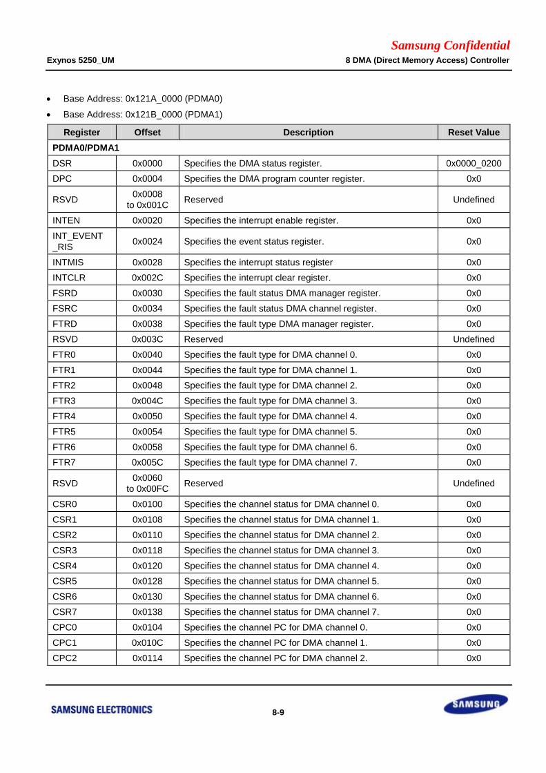
Samsung Confidential Exynos 5250_UM 8 DMA (Direct Memory Access) Controller
8-9
Base Address: 0x121A_0000 (PDMA0)
Base Address: 0x121B_0000 (PDMA1)
Register Offset Description Reset Value
PDMA0/PDMA1
DSR 0x0000 Specifies the DMA status register. 0x0000_0200
DPC 0x0004 Specifies the DMA program counter register. 0x0
RSVD 0x0008
to 0x001C Reserved Undefined
INTEN 0x0020 Specifies the interrupt enable register. 0x0
INT_EVENT
_RIS 0x0024 Specifies the event status register. 0x0
INTMIS 0x0028 Specifies the interrupt status register 0x0
INTCLR 0x002C Specifies the interrupt clear register. 0x0
FSRD 0x0030 Specifies the fault status DMA manager register. 0x0
FSRC 0x0034 Specifies the fault status DMA channel register. 0x0
FTRD 0x0038 Specifies the fault type DMA manager register. 0x0
RSVD 0x003C Reserved Undefined
FTR0 0x0040 Specifies the fault type for DMA channel 0. 0x0
FTR1 0x0044 Specifies the fault type for DMA channel 1. 0x0
FTR2 0x0048 Specifies the fault type for DMA channel 2. 0x0
FTR3 0x004C Specifies the fault type for DMA channel 3. 0x0
FTR4 0x0050 Specifies the fault type for DMA channel 4. 0x0
FTR5 0x0054 Specifies the fault type for DMA channel 5. 0x0
FTR6 0x0058 Specifies the fault type for DMA channel 6. 0x0
FTR7 0x005C Specifies the fault type for DMA channel 7. 0x0
RSVD 0x0060
to 0x00FC Reserved Undefined
CSR0 0x0100 Specifies the channel status for DMA channel 0. 0x0
CSR1 0x0108 Specifies the channel status for DMA channel 1. 0x0
CSR2 0x0110 Specifies the channel status for DMA channel 2. 0x0
CSR3 0x0118 Specifies the channel status for DMA channel 3. 0x0
CSR4 0x0120 Specifies the channel status for DMA channel 4. 0x0
CSR5 0x0128 Specifies the channel status for DMA channel 5. 0x0
CSR6 0x0130 Specifies the channel status for DMA channel 6. 0x0
CSR7 0x0138 Specifies the channel status for DMA channel 7. 0x0
CPC0 0x0104 Specifies the channel PC for DMA channel 0. 0x0
CPC1 0x010C Specifies the channel PC for DMA channel 1. 0x0
CPC2 0x0114 Specifies the channel PC for DMA channel 2. 0x0

Samsung Confidential Exynos 5250_UM 8 DMA (Direct Memory Access) Controller
8-10
Register Offset Description Reset Value
CPC3 0x011C Specifies the channel PC for DMA channel 3. 0x0
CPC4 0x0124 Specifies the channel PC for DMA channel 4. 0x0
CPC5 0x012C Specifies the channel PC for DMA channel 5. 0x0
CPC6 0x0134 Specifies the channel PC for DMA channel 6. 0x0
CPC7 0x013C Specifies the channel PC for DMA channel 7. 0x0
RSVD 0x0140
to 0x03FC Reserved Undefined
SAR_0 0x0400 Specifies the source address for DMA channel 0. 0x0
SAR_1 0x0420 Specifies the source address for DMA channel 1. 0x0
SAR_2 0x0440 Specifies the source address for DMA channel 2. 0x0
SAR_3 0x0460 Specifies the source address for DMA channel 3. 0x0
SAR_4 0x0480 Specifies the source address For DMA channel 4. 0x0
SAR_5 0x04A0 Specifies the source address for DMA channel 5. 0x0
SAR_6 0x04C0 Specifies the Source address for DMA channel 6. 0x0
SAR_7 0x04E0 Specifies the source address for DMA channel 7. 0x0
DAR_0 0x0404 Specifies the destination address for DMA channel 0. 0x0
DAR_1 0x0424 Specifies the destination address for DMA channel 1. 0x0
DAR_2 0x0444 Specifies the destination address for DMA channel 2. 0x0
DAR_3 0x0464 Specifies the destination address for DMA channel 3. 0x0
DAR_4 0x0484 Specifies the destination address for DMA channel 4. 0x0
DAR_5 0x04A4 Specifies the destination address for DMA channel 5. 0x0
DAR_6 0x04C4 Specifies the destination address for DMA channel 6. 0x0
DAR_7 0x04E4 Specifies the destination address for DMA channel 7. 0x0
CCR_0 0x0408 Specifies the channel control for DMA channel 0. 0x0
CCR_1 0x0428 Specifies the channel control for DMA channel 1. 0x0
CCR_2 0x0448 Specifies the channel control for DMA channel 2. 0x0
CCR_3 0x0468 Specifies the channel control for DMA channel 3. 0x0
CCR_4 0x0488 Specifies the channel control for DMA channel 4. 0x0
CCR_5 0x04A8 Specifies the channel control for DMA channel 5. 0x0
CCR_6 0x04C8 Specifies the channel control for DMA channel 6. 0x0
CCR_7 0x04E8 Specifies the channel control for DMA channel 7. 0x0
LC0_0 0x040C Specifies the loop counter 0 for DMA channel 0. 0x0
LC0_1 0x042C Specifies the loop counter 0 for DMA channel 1. 0x0
LC0_2 0x044C Specifies the loop counter 0 for DMA channel 2. 0x0
LC0_3 0x046C Specifies the loop counter 0 for DMA channel 3. 0x0
LC0_4 0x048C Specifies the loop counter 0 for DMA channel 4. 0x0
LC0_5 0x04AC Specifies the loop counter 0 for DMA channel 5. 0x0
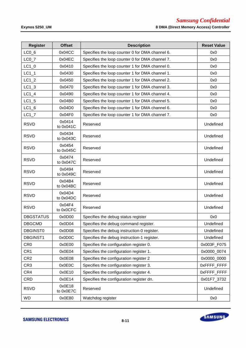
Samsung Confidential Exynos 5250_UM 8 DMA (Direct Memory Access) Controller
8-11
Register Offset Description Reset Value
LC0_6 0x04CC Specifies the loop counter 0 for DMA channel 6. 0x0
LC0_7 0x04EC Specifies the loop counter 0 for DMA channel 7. 0x0
LC1_0 0x0410 Specifies the loop counter 1 for DMA channel 0. 0x0
LC1_1 0x0430 Specifies the loop counter 1 for DMA channel 1. 0x0
LC1_2 0x0450 Specifies the loop counter 1 for DMA channel 2. 0x0
LC1_3 0x0470 Specifies the loop counter 1 for DMA channel 3. 0x0
LC1_4 0x0490 Specifies the loop counter 1 for DMA channel 4. 0x0
LC1_5 0x04B0 Specifies the loop counter 1 for DMA channel 5. 0x0
LC1_6 0x04D0 Specifies the loop counter 1 for DMA channel 6. 0x0
LC1_7 0x04F0 Specifies the loop counter 1 for DMA channel 7. 0x0
RSVD 0x0414
to 0x041C Reserved Undefined
RSVD 0x0434
to 0x043C Reserved Undefined
RSVD 0x0454
to 0x045C Reserved Undefined
RSVD 0x0474
to 0x047C Reserved Undefined
RSVD 0x0494
to 0x049C Reserved Undefined
RSVD 0x04B4
to 0x04BC Reserved Undefined
RSVD 0x04D4
to 0x04DC Reserved Undefined
RSVD 0x04F4
to 0x0CFC Reserved Undefined
DBGSTATUS 0x0D00 Specifies the debug status register 0x0
DBGCMD 0x0D04 Specifies the debug command register. Undefined
DBGINST0 0x0D08 Specifies the debug instruction-0 register. Undefined
DBGINST1 0x0D0C Specifies the debug instruction-1 register. Undefined
CR0 0x0E00 Specifies the configuration register 0. 0x003F_F075
CR1 0x0E04 Specifies the configuration register 1. 0x0000_0074
CR2 0x0E08 Specifies the configuration register 2 0x0000_0000
CR3 0x0E0C Specifies the configuration register 3. 0xFFFF_FFFF
CR4 0x0E10 Specifies the configuration register 4. 0xFFFF_FFFF
CRD 0x0E14 Specifies the configuration register dn. 0x01F7_3732
RSVD 0x0E18
to 0x0E7C Reserved Undefined
WD 0x0E80 Watchdog register 0x0

Samsung Confidential Exynos 5250_UM 8 DMA (Direct Memory Access) Controller
8-12
Register Offset Description Reset Value
periph_id_n 0x0FE0
to 0x0FEC Specifies the peripheral identification registers 0-3.
Configuration-
dependent
pcell_id_n 0x0FF0
to 0x0FFC Specifies the prime cell identification registers 0-3.
Configuration-
dependent
NOTE: The SFR provides description for only the restricted and fixed part of some SFR. DMA330 TRM provides detailed
information of other parts and other SFRs.
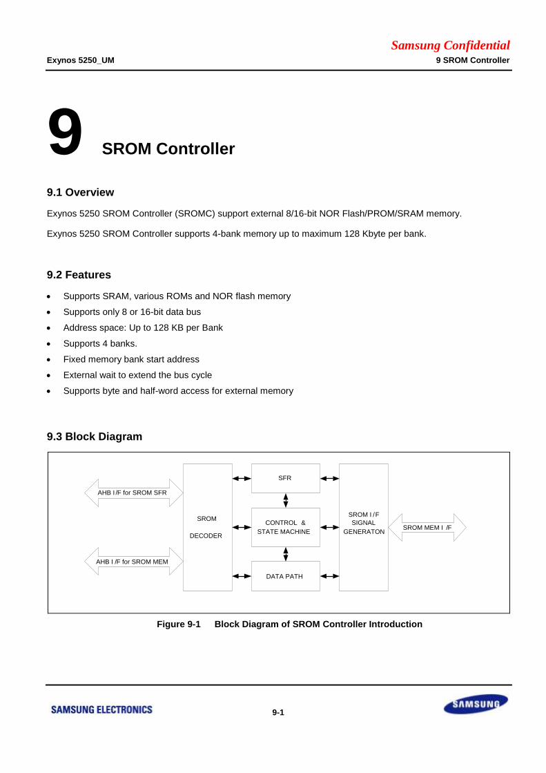
Samsung Confidential Exynos 5250_UM 9 SROM Controller
9-1
9 SROM Controller
9.1 Overview
Exynos 5250 SROM Controller (SROMC) support external 8/16-bit NOR Flash/PROM/SRAM memory.
Exynos 5250 SROM Controller supports 4-bank memory up to maximum 128 Kbyte per bank.
9.2 Features
Supports SRAM, various ROMs and NOR flash memory
Supports only 8 or 16-bit data bus
Address space: Up to 128 KB per Bank
Supports 4 banks.
Fixed memory bank start address
External wait to extend the bus cycle
Supports byte and half-word access for external memory
9.3 Block Diagram
Figure 9-1 Block Diagram of SROM Controller Introduction
SROM
DECODER
SFR
CONTROL &
STATE MACHINE
SROM I /F
SIGNAL
GENERATON
AHB I /F for SROM SFR
AHB I /F for SROM MEM
SROM MEM I /F
DATA PATH
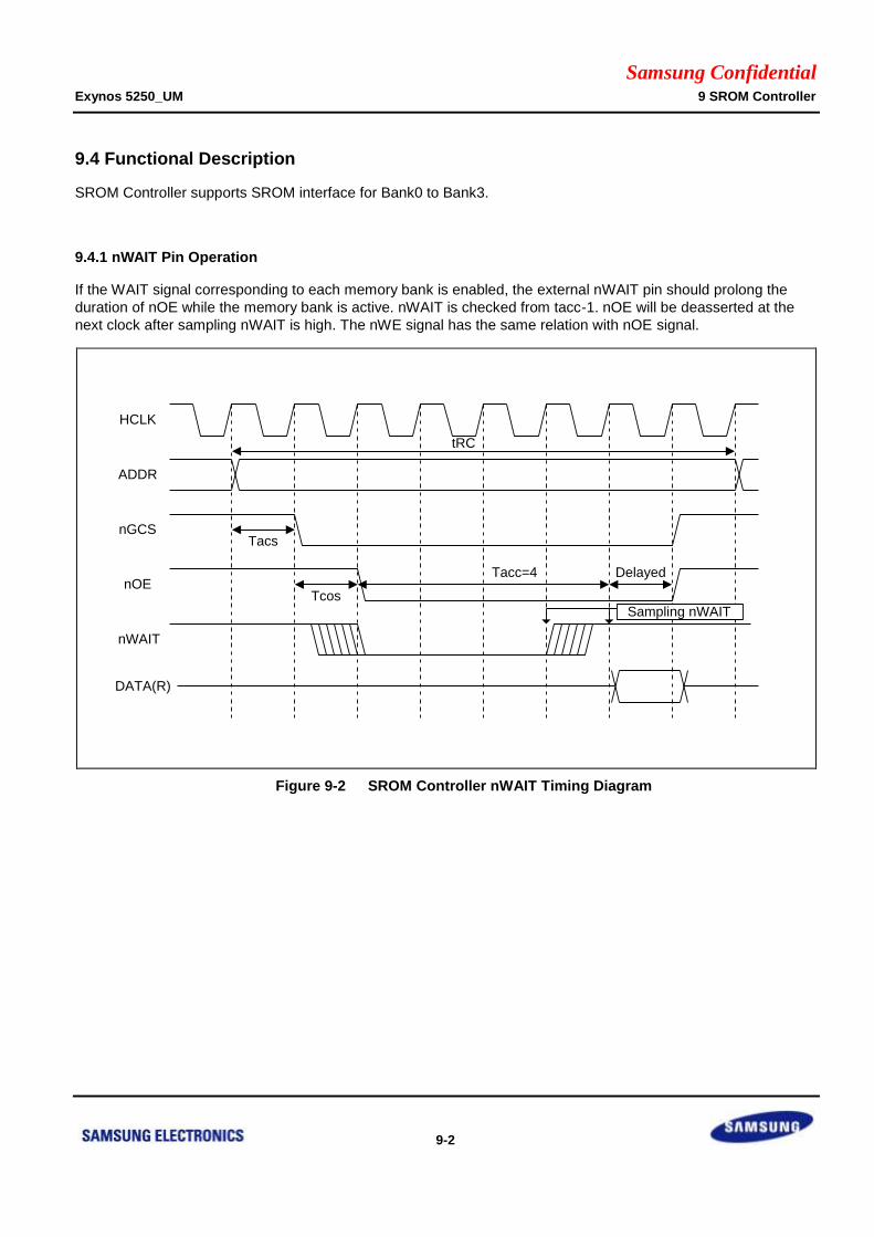
Samsung Confidential Exynos 5250_UM 9 SROM Controller
9-2
9.4 Functional Description
SROM Controller supports SROM interface for Bank0 to Bank3.
9.4.1 nWAIT Pin Operation
If the WAIT signal corresponding to each memory bank is enabled, the external nWAIT pin should prolong the
duration of nOE while the memory bank is active. nWAIT is checked from tacc-1. nOE will be deasserted at the
next clock after sampling nWAIT is high. The nWE signal has the same relation with nOE signal.
Figure 9-2 SROM Controller nWAIT Timing Diagram
tRC
Tacs
Tcos
Tacc=4
HCLK
ADDR
nGCS
nOE
nWAIT
DATA(R)
Delayed
Sampling nWAIT
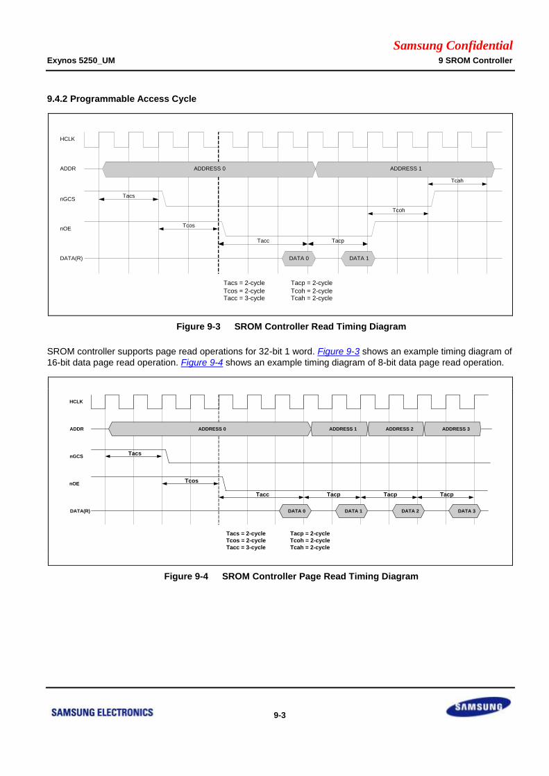
Samsung Confidential Exynos 5250_UM 9 SROM Controller
9-3
9.4.2 Programmable Access Cycle
Figure 9-3 SROM Controller Read Timing Diagram
SROM controller supports page read operations for 32-bit 1 word. Figure 9-3 shows an example timing diagram of
16-bit data page read operation. Figure 9-4 shows an example timing diagram of 8-bit data page read operation.
HCLK
ADDR
nGCS
DATA(R)
Tacs
Tacc
ADDRESS 0
DATA 0
nOETcos
Tacp
DATA 1
ADDRESS 1
Tacs = 2-cycle Tacp = 2-cycle
Tcos = 2-cycle Tcoh = 2-cycle
Tacc = 3-cycle Tcah = 2-cycle
Tacp
DATA 2
Tacp
DATA 3
ADDRESS 2 ADDRESS 3
Figure 9-4 SROM Controller Page Read Timing Diagram
HCLK
ADDR
nGCS
DATA(R)
Tacs
Tacc
Tcoh
Tcah
ADDRESS 0
DATA 0
nOETcos
Tacp
DATA 1
ADDRESS 1
Tacs = 2-cycle Tacp = 2-cycle
Tcos = 2-cycle Tcoh = 2-cycleTacc = 3-cycle Tcah = 2-cycle
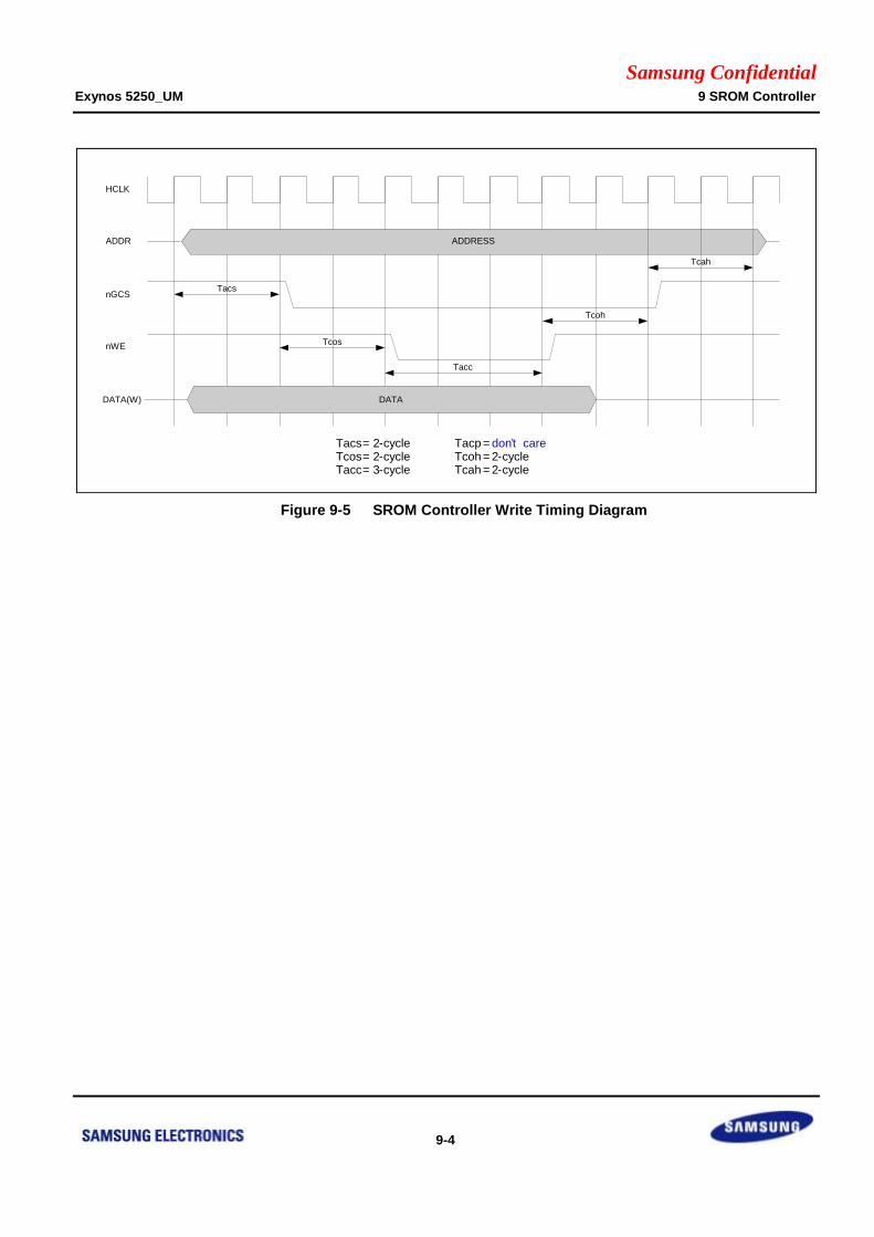
Samsung Confidential Exynos 5250_UM 9 SROM Controller
9-4
Figure 9-5 SROM Controller Write Timing Diagram
HCLK
ADDR
nGCS
DATA(W)
Tacs
Tacc
Tcoh
Tcah
ADDRESS
nWETcos
DATA
Tacs= 2-cycle Tacp = don’t careTcos= 2-cycle Tcoh = 2-cycleTacc= 3-cycle Tcah = 2-cycle
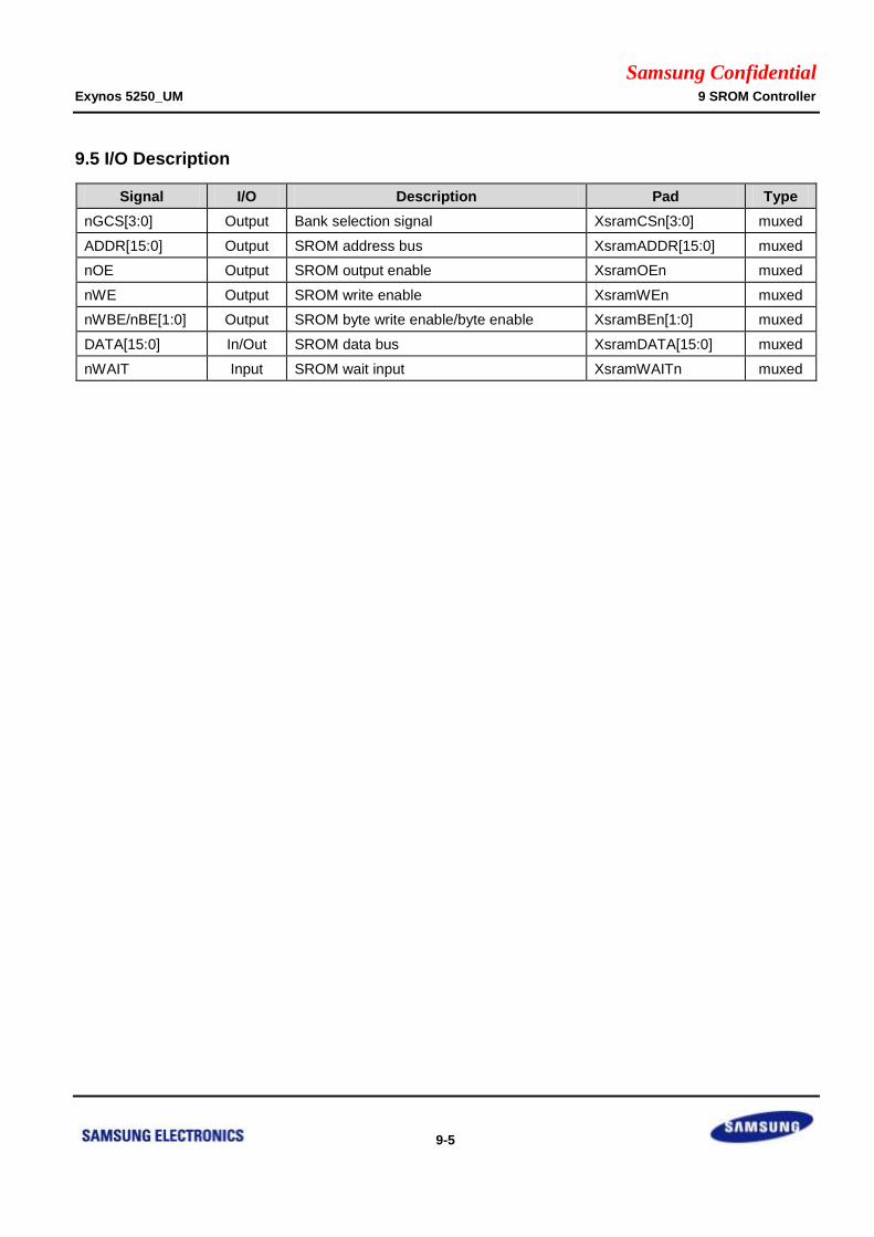
Samsung Confidential Exynos 5250_UM 9 SROM Controller
9-5
9.5 I/O Description
Signal I/O Description Pad Type
nGCS[3:0] Output Bank selection signal XsramCSn[3:0] muxed
ADDR[15:0] Output SROM address bus XsramADDR[15:0] muxed
nOE Output SROM output enable XsramOEn muxed
nWE Output SROM write enable XsramWEn muxed
nWBE/nBE[1:0] Output SROM byte write enable/byte enable XsramBEn[1:0] muxed
DATA[15:0] In/Out SROM data bus XsramDATA[15:0] muxed
nWAIT Input SROM wait input XsramWAITn muxed
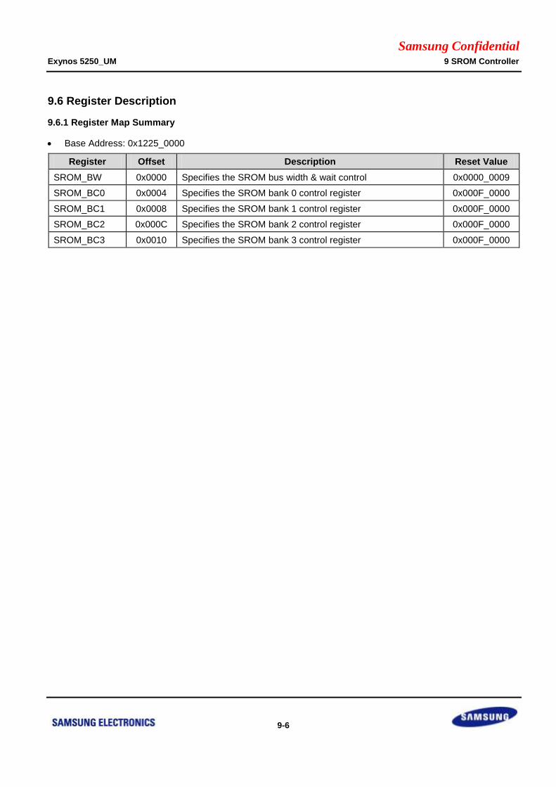
Samsung Confidential Exynos 5250_UM 9 SROM Controller
9-6
9.6 Register Description
9.6.1 Register Map Summary
Base Address: 0x1225_0000
Register Offset Description Reset Value
SROM_BW 0x0000 Specifies the SROM bus width & wait control 0x0000_0009
SROM_BC0 0x0004 Specifies the SROM bank 0 control register 0x000F_0000
SROM_BC1 0x0008 Specifies the SROM bank 1 control register 0x000F_0000
SROM_BC2 0x000C Specifies the SROM bank 2 control register 0x000F_0000
SROM_BC3 0x0010 Specifies the SROM bank 3 control register 0x000F_0000
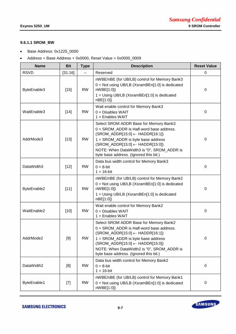
Samsung Confidential Exynos 5250_UM 9 SROM Controller
9-7
9.6.1.1 SROM_BW
Base Address: 0x1225_0000
Address = Base Address + 0x0000, Reset Value = 0x0000_0009
Name Bit Type Description Reset Value
RSVD [31:16] – Reserved 0
ByteEnable3 [15] RW
nWBE/nBE (for UB/LB) control for Memory Bank3
0 = Not using UB/LB (XsramBEn[1:0] is dedicated
nWBE[1:0])
1 = Using UB/LB (XsramBEn[1:0] is dedicated
nBE[1:0])
0
WaitEnable3 [14] RW
Wait enable control for Memory Bank3
0 = Disables WAIT
1 = Enables WAIT
0
AddrMode3 [13] RW
Select SROM ADDR Base for Memory Bank3
0 = SROM_ADDR is Half-word base address.
(SROM_ADDR[15:0] HADDR[16:1])
1 = SROM_ADDR is byte base address
(SROM_ADDR[15:0] HADDR[15:0])
NOTE: When DataWidth3 is "0", SROM_ADDR is
byte base address. (Ignored this bit.)
0
DataWidth3 [12] RW
Data bus width control for Memory Bank3
0 = 8-bit
1 = 16-bit
0
ByteEnable2 [11] RW
nWBE/nBE (for UB/LB) control for Memory Bank2
0 = Not using UB/LB (XsramBEn[1:0] is dedicated
nWBE[1:0])
1 = Using UB/LB (XsramBEn[1:0] is dedicated
nBE[1:0])
0
WaitEnable2 [10] RW
Wait enable control for Memory Bank2
0 = Disables WAIT
1 = Enables WAIT
0
AddrMode2 [9] RW
Select SROM ADDR Base for Memory Bank2
0 = SROM_ADDR is Half-word base address.
(SROM_ADDR[15:0] HADDR[16:1])
1 = SROM_ADDR is byte base address
(SROM_ADDR[15:0] HADDR[15:0])
NOTE: When DataWidth2 is "0", SROM_ADDR is
byte base address. (Ignored this bit.)
0
DataWidth2 [8] RW
Data bus width control for Memory Bank2
0 = 8-bit
1 = 16-bit
0
ByteEnable1 [7] RW
nWBE/nBE (for UB/LB) control for Memory Bank1
0 = Not using UB/LB (XsramBEn[1:0] is dedicated
nWBE[1:0])
0
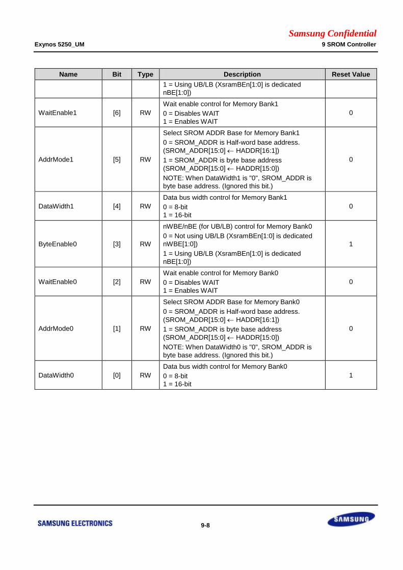
Samsung Confidential Exynos 5250_UM 9 SROM Controller
9-8
Name Bit Type Description Reset Value
1 = Using UB/LB (XsramBEn[1:0] is dedicated
nBE[1:0])
WaitEnable1 [6] RW
Wait enable control for Memory Bank1
0 = Disables WAIT
1 = Enables WAIT
0
AddrMode1 [5] RW
Select SROM ADDR Base for Memory Bank1
0 = SROM_ADDR is Half-word base address.
(SROM_ADDR[15:0] HADDR[16:1])
1 = SROM_ADDR is byte base address
(SROM_ADDR[15:0] HADDR[15:0])
NOTE: When DataWidth1 is "0", SROM_ADDR is
byte base address. (Ignored this bit.)
0
DataWidth1 [4] RW
Data bus width control for Memory Bank1
0 = 8-bit
1 = 16-bit
0
ByteEnable0 [3] RW
nWBE/nBE (for UB/LB) control for Memory Bank0
0 = Not using UB/LB (XsramBEn[1:0] is dedicated
nWBE[1:0])
1 = Using UB/LB (XsramBEn[1:0] is dedicated
nBE[1:0])
1
WaitEnable0 [2] RW
Wait enable control for Memory Bank0
0 = Disables WAIT
1 = Enables WAIT
0
AddrMode0 [1] RW
Select SROM ADDR Base for Memory Bank0
0 = SROM_ADDR is Half-word base address.
(SROM_ADDR[15:0] HADDR[16:1])
1 = SROM_ADDR is byte base address
(SROM_ADDR[15:0] HADDR[15:0])
NOTE: When DataWidth0 is "0", SROM_ADDR is
byte base address. (Ignored this bit.)
0
DataWidth0 [0] RW
Data bus width control for Memory Bank0
0 = 8-bit
1 = 16-bit
1
Samsung Confidential Exynos 5250_UM 9 SROM Controller
9-9
9.6.1.2 SROM_BCn (n = 0 to 3)
Base Address: 0x1225_0000
Address = Base Address + 0x0004, 0x0008, 0x000C, 0x0010, Reset Value = 0x000F_0000
Name Bit Type Description Reset Value
Tacs [31:28] RW
Address set-up before nGCS
0000 = 0 Clock
0001 = 1 Clocks
0010 = 2 Clocks
0011 = 3 Clocks
………….
1100 = 12 Clocks
1101 = 13 Clocks
1110 = 14 Clocks
1111 = 15 Clocks
NOTE: More 1 – 2 cycles according to bus i/f status
0000
Tcos [27:24] RW
Chip selection set-up before nOE
0000 = 0 Clock
0001 = 1 Clocks
0010 = 2 Clocks
0011 = 3 Clocks
………….
1100 = 12 Clocks
1101 = 13 Clocks
1110 = 14 Clocks
1111 = 15 Clocks
0000
RSVD [23:21] – Reserved 000
Tacc [20:16] RW
Access cycle
00000 = 1 Clock
00001 = 2 Clocks
00001 = 3 Clocks
00010 = 4 Clocks
………….
11100 = 29 Clocks
11101 = 30 Clocks
11110 = 31 Clocks
11111 = 32 Clocks
01111
Tcoh [15:12] RW
Chip selection hold on nOE
0000 = 0 Clock
0001 = 1 Clocks
0010 = 2 Clocks
0011 = 3 Clocks
………….
1100 = 12 Clocks
1101 = 13 Clocks
1110 = 14 Clocks
1111 = 15 Clocks
0000
Samsung Confidential Exynos 5250_UM 9 SROM Controller
9-10
Name Bit Type Description Reset Value
Tcah [11:8] RW
Address holding time after nGCSn
0000 = 0 Clock
0001 = 1 Clocks
0010 = 2 Clocks
0011 = 3 Clocks
………….
1100 = 12 Clocks
1101 = 13 Clocks
1110 = 14 Clocks
1111 = 15 Clocks
NOTE: More 1 – 2 cycles according to bus I/F status
0000
Tacp [7:4] RW
Page mode access cycle @ Page mode
0000 = 0 Clock
0001 = 1 Clocks
0010 = 2 Clocks
0011 = 3 Clocks
………….
1100 = 12 Clocks
1101 = 13 Clocks
1110 = 14 Clocks
1111 = 15 Clocks
0000
RSVD [3:2] – Reserved –
PMC [1:0] RW
Page mode configuration
00 = Normal (1 Data)
01 = 4 Data
10 = Reserved
11 = Reserved
00
Samsung Confidential Exynos 5250_UM 10 Pulse Width Modulation Timer
10-1
10 Pulse Width Modulation Timer
10.1 Overview
The Exynos 5250 has five 32-bit Pulse Width Modulation (PWM) timers. These Timers generate internal interrupts
for the ARM subsystem. Additionally, Timers 0, 1, 2 and 3 include a PWM function that drives an external I/O
signal. The PWM in Timer 0 has an optional dead-zone generator capability to support a large current device.
Timer 4 is internal timer without output pins.
The Timers use the APB-PCLK as source clock. Timers 0 and 1 share a programmable 8-bit prescaler that
provides the first level of division for the PCLK. Timers 2, 3, and 4 share a different 8-bit prescaler. Each timer has
its own private clock-divider that provides a second level of clock division (prescaler divided by 2, 4, 8, or 16).
Each Timer has its own 32-bit down-counter which is driven by the timer clock. The down-counter is initially
loaded from the Timer Count Buffer register (TCNTBn). When the down-counter reaches zero, the timer interrupt
request is generated to inform the CPU that the Timer operation is complete. When the Timer down-counter
reaches zero, the value of corresponding TCNTBn automatically reloads into the down-counter to start the next
cycle. However, when the Timer stops, for example, by clearing the timer enable bit of TCONn during the Timer
running mode, the value of TCNTBn is not reloaded into the counter.
The PWM function uses the value of the TCMPBn register. The Timer Control Logic changes the output level if
down-counter value matches the value of the compare register in Timer Control Logic. Therefore, the compare
register determines the turn-on time or turn-off time of a PWM output.
The TCNTBn and TCMPBn registers are double buffered so that it allows the Timer parameters to be updated in
the middle of a cycle. The new values do not take effect until the current Timer cycle is completed.
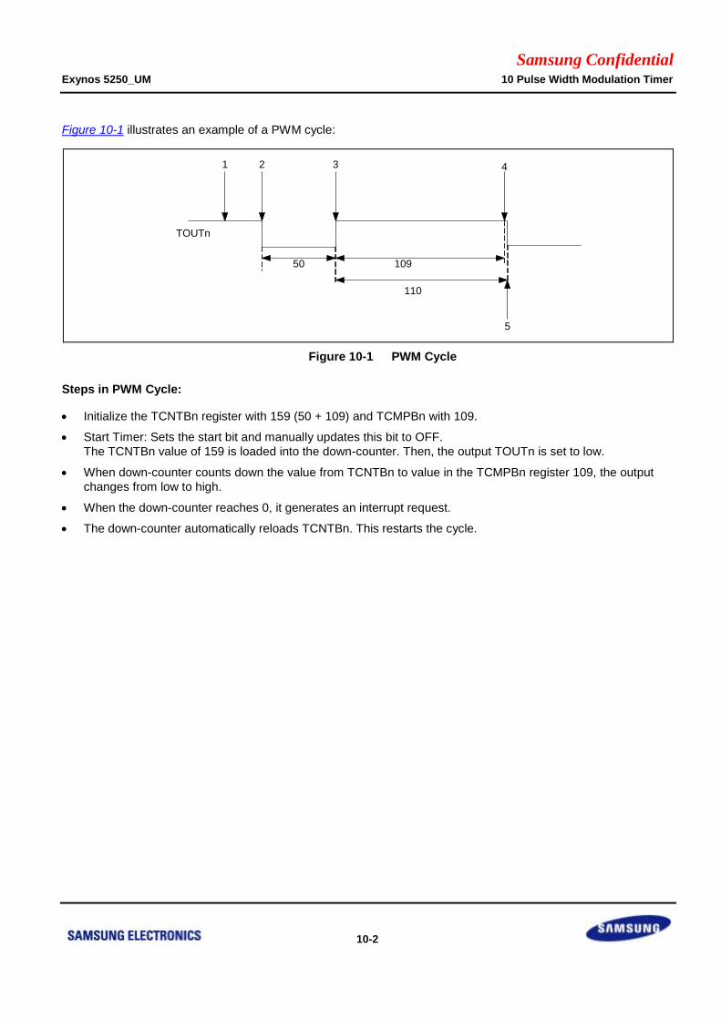
Samsung Confidential Exynos 5250_UM 10 Pulse Width Modulation Timer
10-2
Figure 10-1 illustrates an example of a PWM cycle:
Figure 10-1 PWM Cycle
Steps in PWM Cycle:
Initialize the TCNTBn register with 159 (50 + 109) and TCMPBn with 109.
Start Timer: Sets the start bit and manually updates this bit to OFF.
The TCNTBn value of 159 is loaded into the down-counter. Then, the output TOUTn is set to low.
When down-counter counts down the value from TCNTBn to value in the TCMPBn register 109, the output
changes from low to high.
When the down-counter reaches 0, it generates an interrupt request.
The down-counter automatically reloads TCNTBn. This restarts the cycle.
TOUTn
1 2 3 4
5
50 109
110
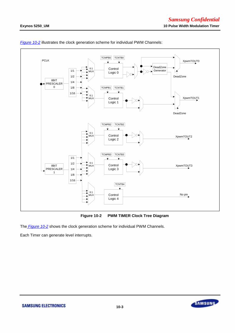
Samsung Confidential Exynos 5250_UM 10 Pulse Width Modulation Timer
10-3
Figure 10-2 illustrates the clock generation scheme for individual PWM Channels:
6:1
MUXControl
Logic 0
Control
Logic 4
Control
Logic 3
Control
Logic 2
Control
Logic 1
8BIT
PRESCALER
0
DeadZone
Generator
TCNTB0TCMPB0
TCNTB1TCMPB1
TCNTB2TCMPB2
TCNTB3TCMPB3
TCNTB4
8BIT
PRESCALER
1
6:1
MUX
6:1
MUX
6:1
MUX
6:1
MUX
PCLK XpwmTOUT0
No pin
DeadZone
1/1
1/2
1/16
1/8
1/4
1/1
1/2
1/16
1/8
1/4
DeadZone
XpwmTOUT1
XpwmTOUT3
XpwmTOUT2
Figure 10-2 PWM TIMER Clock Tree Diagram
The Figure 10-2 shows the clock generation scheme for individual PWM Channels.
Each Timer can generate level interrupts.
Samsung Confidential Exynos 5250_UM 10 Pulse Width Modulation Timer
10-4
10.2 Features
PWM supports these features:
Five 32-bit Timers
Two 8-bit Clock Prescalers that provide first level of division for the PCLK, and five Clock Dividers and
Multiplexers that provide second level of division for the Prescaler clock
Programmable Clock Select Logic for individual PWM Channels
Four Independent PWM Channels with Programmable Duty Control and Polarity
Static Configuration: PWM is stopped
Dynamic Configuration: PWM is running
Auto-Reload and One-Shot Pulse Mode
Dead Zone Generator on two PWM Outputs
Level Interrupt Generation
The PWM has two modes of operation:
Auto-Reload Mode: In this mode, continuous PWM pulses are generated based on Programmed Duty Cycle
and Polarity.
One-Shot Pulse Mode: In this mode, only one PWM pulse is generated based on Programmed Duty Cycle
and Polarity.
To control the functionality of PWM, 18 special function registers are provided. The PWM is a programmable
output and a clock input AMBA slave module. It connects to the Advanced Peripheral Bus (APB). These 18
special function registers within PWM are accessed through APB transactions.
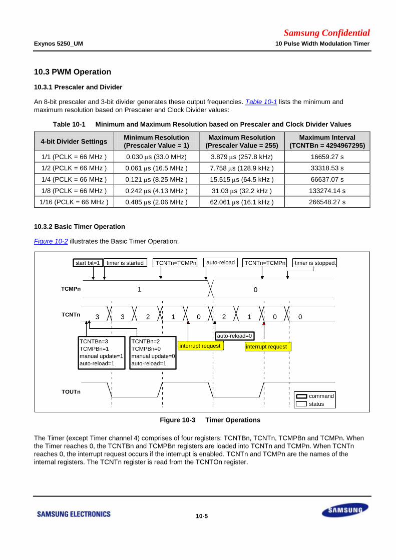
Samsung Confidential Exynos 5250_UM 10 Pulse Width Modulation Timer
10-5
10.3 PWM Operation
10.3.1 Prescaler and Divider
An 8-bit prescaler and 3-bit divider generates these output frequencies. Table 10-1 lists the minimum and
maximum resolution based on Prescaler and Clock Divider values:
Table 10-1 Minimum and Maximum Resolution based on Prescaler and Clock Divider Values
4-bit Divider Settings Minimum Resolution
(Prescaler Value = 1)
Maximum Resolution
(Prescaler Value = 255)
Maximum Interval
(TCNTBn = 4294967295)
1/1 (PCLK = 66 MHz ) 0.030 s (33.0 MHz) 3.879 s (257.8 kHz) 16659.27 s
1/2 (PCLK = 66 MHz ) 0.061 s (16.5 MHz ) 7.758 s (128.9 kHz ) 33318.53 s
1/4 (PCLK = 66 MHz ) 0.121 s (8.25 MHz ) 15.515 s (64.5 kHz ) 66637.07 s
1/8 (PCLK = 66 MHz ) 0.242 s (4.13 MHz ) 31.03 s (32.2 kHz ) 133274.14 s
1/16 (PCLK = 66 MHz ) 0.485 s (2.06 MHz ) 62.061 s (16.1 kHz ) 266548.27 s
10.3.2 Basic Timer Operation
Figure 10-2 illustrates the Basic Timer Operation:
Figure 10-3 Timer Operations
The Timer (except Timer channel 4) comprises of four registers: TCNTBn, TCNTn, TCMPBn and TCMPn. When
the Timer reaches 0, the TCNTBn and TCMPBn registers are loaded into TCNTn and TCMPn. When TCNTn
reaches 0, the interrupt request occurs if the interrupt is enabled. TCNTn and TCMPn are the names of the
internal registers. The TCNTn register is read from the TCNTOn register.
3 3 2
01
1 0 2 1 0 0
TCNTBn=2
TCMPBn=0
manual update=0
auto-reload=1
interrupt requestinterrupt requestTCNTBn=3
TCMPBn=1
manual update=1
auto-reload=1
TOUTn
TCMPn
TCNTn
auto-reload=0
command
status
timer is started TCNTn=TCMPn auto-reloadstart bit=1 TCNTn=TCMPn timer is stopped.
Samsung Confidential Exynos 5250_UM 10 Pulse Width Modulation Timer
10-6
To generate interrupt at intervals three-cycle of XpwmTOUTn, set TCNTBn, TCMPBn and TCON.
Steps to generate interrupt:
1. Set TCNTBn = 3 and TCMPBn = 1.
2. Set auto-reload = 1 and manual update = 1.
When manual update bit is 1, the TCNTBn and TCMPBn values are loaded to TCNTn and TCMPn.
3. Set TCNTBn = 2 and TCMPBn = 0 for the next operation.
4. Set auto-reload = 1 and manual update = 0.
If you set manual update = 1, TCNTn is changed to 2 and TCMP is changed to 0.
Therefore, interrupt is generated at interval two-cycle instead of three-cycle.
Set auto-reload = 1 automatically, for the next operation.
5. Set start = 1 for starting the operation. Then, TCNTn is down counting.
When TCNTn is 0, interrupt is generated and if auto-reload is enable, TCNTn is loaded 2 (TCNTBn value)
and TCMPn is loaded 0 (TCMPn value).
6. TCNTn is down counting before it stops.
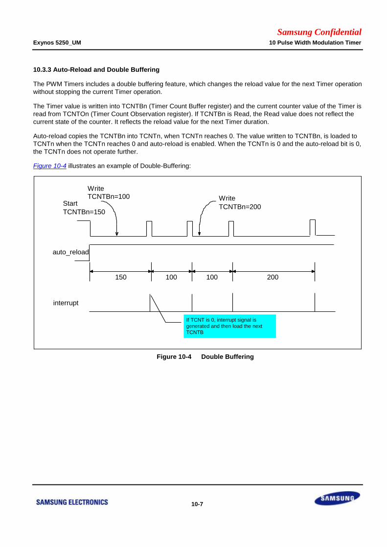
Samsung Confidential Exynos 5250_UM 10 Pulse Width Modulation Timer
10-7
10.3.3 Auto-Reload and Double Buffering
The PWM Timers includes a double buffering feature, which changes the reload value for the next Timer operation
without stopping the current Timer operation.
The Timer value is written into TCNTBn (Timer Count Buffer register) and the current counter value of the Timer is
read from TCNTOn (Timer Count Observation register). If TCNTBn is Read, the Read value does not reflect the
current state of the counter. It reflects the reload value for the next Timer duration.
Auto-reload copies the TCNTBn into TCNTn, when TCNTn reaches 0. The value written to TCNTBn, is loaded to
TCNTn when the TCNTn reaches 0 and auto-reload is enabled. When the TCNTn is 0 and the auto-reload bit is 0,
the TCNTn does not operate further.
Figure 10-4 illustrates an example of Double-Buffering:
Figure 10-4 Double Buffering
WriteTCNTBn=100 Write
TCNTBn=200Start
auto_reload
TCNTBn=150
150 200100100
interrupt
If TCNT is 0, interrupt signal is
generated and then load the next
TCNTB
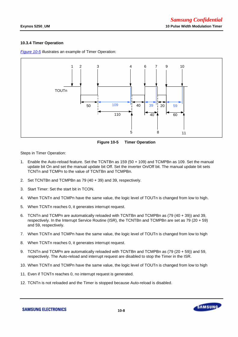
Samsung Confidential Exynos 5250_UM 10 Pulse Width Modulation Timer
10-8
10.3.4 Timer Operation
Figure 10-5 illustrates an example of Timer Operation:
Figure 10-5 Timer Operation
Steps in Timer Operation:
1. Enable the Auto-reload feature. Set the TCNTBn as 159 (50 + 109) and TCMPBn as 109. Set the manual
update bit On and set the manual update bit Off. Set the inverter On/Off bit. The manual update bit sets
TCNTn and TCMPn to the value of TCNTBn and TCMPBn.
2. Set TCNTBn and TCMPBn as 79 (40 + 39) and 39, respectively.
3. Start Timer: Set the start bit in TCON.
4. When TCNTn and TCMPn have the same value, the logic level of TOUTn is changed from low to high.
5. When TCNTn reaches 0, it generates interrupt request.
6. TCNTn and TCMPn are automatically reloaded with TCNTBn and TCMPBn as (79 (40 + 39)) and 39,
respectively. In the Interrupt Service Routine (ISR), the TCNTBn and TCMPBn are set as 79 (20 + 59)
and 59, respectively.
7. When TCNTn and TCMPn have the same value, the logic level of TOUTn is changed from low to high
8. When TCNTn reaches 0, it generates interrupt request.
9. TCNTn and TCMPn are automatically reloaded with TCNTBn and TCMPBn as (79 (20 + 59)) and 59,
respectively. The Auto-reload and interrupt request are disabled to stop the Timer in the ISR.
10. When TCNTn and TCMPn have the same value, the logic level of TOUTn is changed from low to high
11. Even if TCNTn reaches 0, no interrupt request is generated.
12. TCNTn is not reloaded and the Timer is stopped because Auto-reload is disabled.
TOUTn
1 2 3 4
5
6 7
8
9 10
50 109
110
40 39
40
20
60
59
11
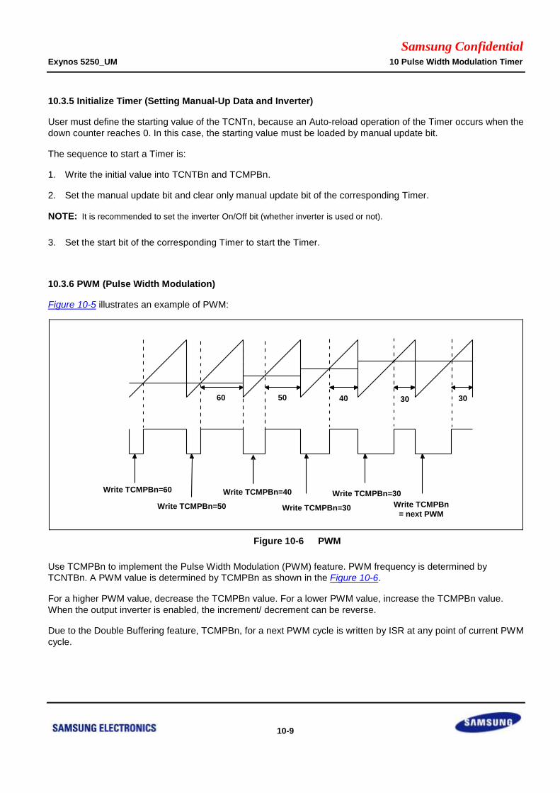
Samsung Confidential Exynos 5250_UM 10 Pulse Width Modulation Timer
10-9
10.3.5 Initialize Timer (Setting Manual-Up Data and Inverter)
User must define the starting value of the TCNTn, because an Auto-reload operation of the Timer occurs when the
down counter reaches 0. In this case, the starting value must be loaded by manual update bit.
The sequence to start a Timer is:
1. Write the initial value into TCNTBn and TCMPBn.
2. Set the manual update bit and clear only manual update bit of the corresponding Timer.
NOTE: It is recommended to set the inverter On/Off bit (whether inverter is used or not).
3. Set the start bit of the corresponding Timer to start the Timer.
10.3.6 PWM (Pulse Width Modulation)
Figure 10-5 illustrates an example of PWM:
Figure 10-6 PWM
Use TCMPBn to implement the Pulse Width Modulation (PWM) feature. PWM frequency is determined by
TCNTBn. A PWM value is determined by TCMPBn as shown in the Figure 10-6.
For a higher PWM value, decrease the TCMPBn value. For a lower PWM value, increase the TCMPBn value.
When the output inverter is enabled, the increment/ decrement can be reverse.
Due to the Double Buffering feature, TCMPBn, for a next PWM cycle is written by ISR at any point of current PWM
cycle.
Write TCMPBn=60
Write TCMPBn=50
Write TCMPBn=40
Write TCMPBn=30
Write TCMPBn=30
Write TCMPBn
= next PWM
60 50 40 30 30
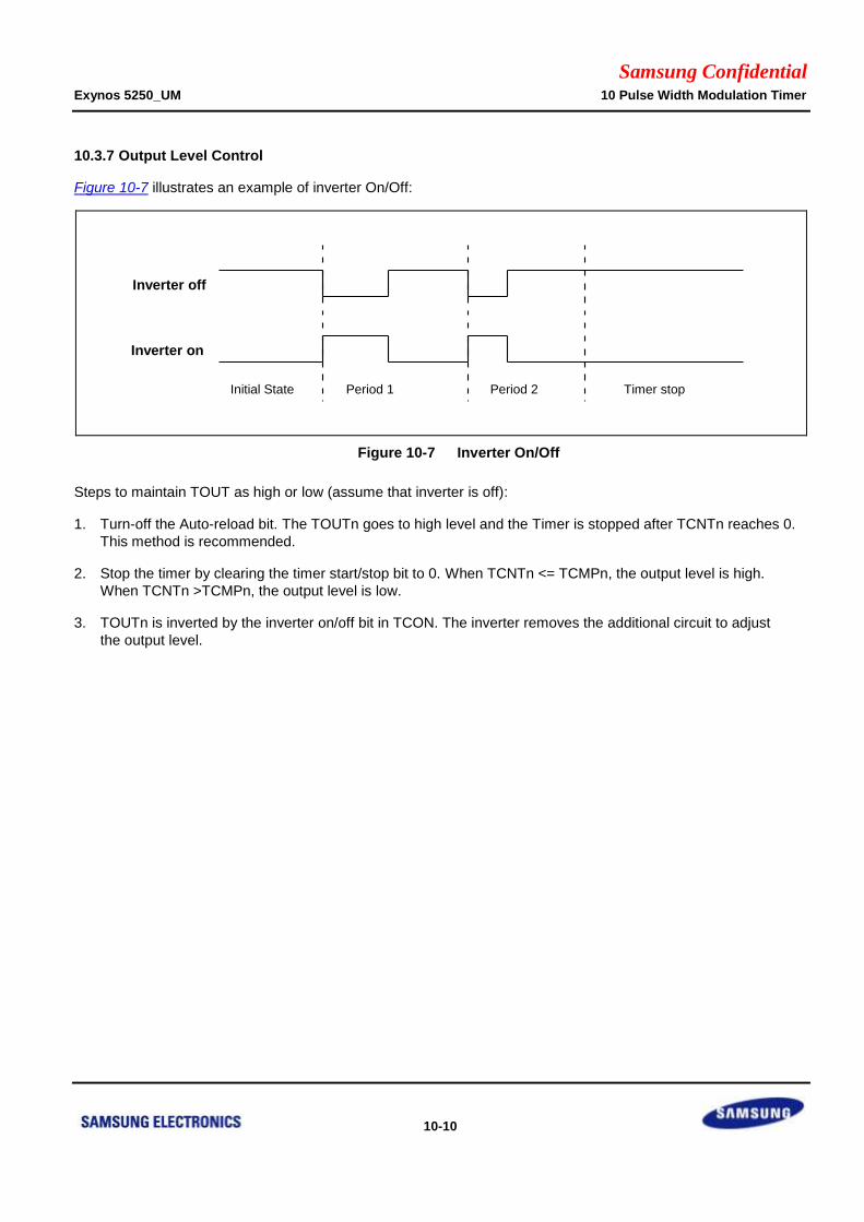
Samsung Confidential Exynos 5250_UM 10 Pulse Width Modulation Timer
10-10
10.3.7 Output Level Control
Figure 10-7 illustrates an example of inverter On/Off:
Figure 10-7 Inverter On/Off
Steps to maintain TOUT as high or low (assume that inverter is off):
1. Turn-off the Auto-reload bit. The TOUTn goes to high level and the Timer is stopped after TCNTn reaches 0.
This method is recommended.
2. Stop the timer by clearing the timer start/stop bit to 0. When TCNTn <= TCMPn, the output level is high.
When TCNTn >TCMPn, the output level is low.
3. TOUTn is inverted by the inverter on/off bit in TCON. The inverter removes the additional circuit to adjust
the output level.
Initial State
Inverter off
Inverter on
Timer stopPeriod 2Period 1
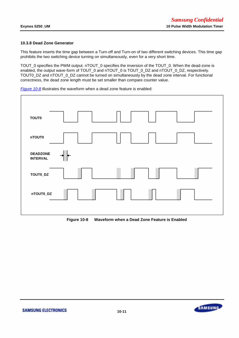
Samsung Confidential Exynos 5250_UM 10 Pulse Width Modulation Timer
10-11
10.3.8 Dead Zone Generator
This feature inserts the time gap between a Turn-off and Turn-on of two different switching devices. This time gap
prohibits the two switching device turning on simultaneously, even for a very short time.
TOUT_0 specifies the PWM output. nTOUT_0 specifies the inversion of the TOUT_0. When the dead-zone is
enabled, the output wave-form of TOUT_0 and nTOUT_0 is TOUT_0_DZ and nTOUT_0_DZ, respectively.
TOUT0_DZ and nTOUT_0_DZ cannot be turned on simultaneously by the dead zone interval. For functional
correctness, the dead zone length must be set smaller than compare counter value.
Figure 10-8 illustrates the waveform when a dead zone feature is enabled:
Figure 10-8 Waveform when a Dead Zone Feature is Enabled
TOUT0
nTOUT0
DEADZONE
INTERVAL
TOUT0_DZ
nTOUT0_DZ

Samsung Confidential Exynos 5250_UM 10 Pulse Width Modulation Timer
10-12
10.4 I/O Description
Signal I/O Description Pad Type
TOUT_0 Output PWMTIMER TOUT[0] XpwmTOUT[0] muxed
TOUT_1 Output PWMTIMER TOUT[1] XpwmTOUT[1] muxed
TOUT_2 Output PWMTIMER TOUT[2] XpwmTOUT[2] muxed
TOUT_3 Output PWMTIMER TOUT[3] XpwmTOUT[3] muxed
NOTE: Type field indicates whether pads are dedicated to the signal, or pads are connected to the multiplexed signals.
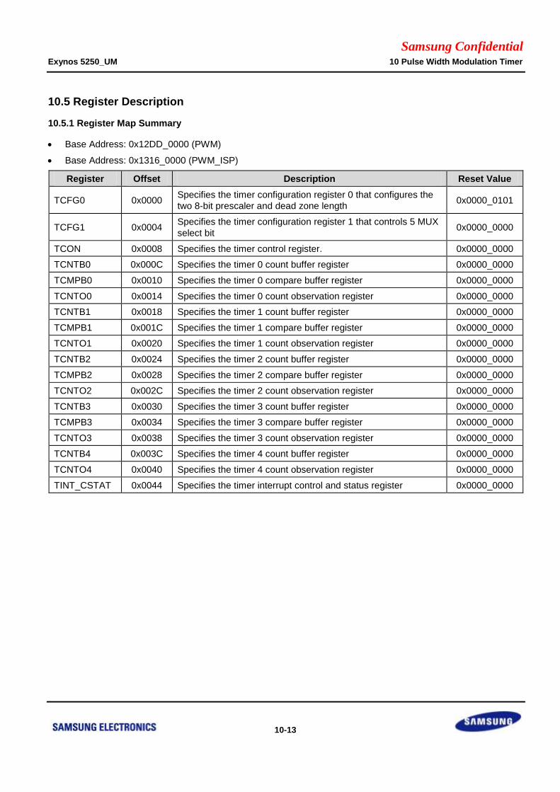
Samsung Confidential Exynos 5250_UM 10 Pulse Width Modulation Timer
10-13
10.5 Register Description
10.5.1 Register Map Summary
Base Address: 0x12DD_0000 (PWM)
Base Address: 0x1316_0000 (PWM_ISP)
Register Offset Description Reset Value
TCFG0 0x0000 Specifies the timer configuration register 0 that configures the
two 8-bit prescaler and dead zone length 0x0000_0101
TCFG1 0x0004 Specifies the timer configuration register 1 that controls 5 MUX
select bit 0x0000_0000
TCON 0x0008 Specifies the timer control register. 0x0000_0000
TCNTB0 0x000C Specifies the timer 0 count buffer register 0x0000_0000
TCMPB0 0x0010 Specifies the timer 0 compare buffer register 0x0000_0000
TCNTO0 0x0014 Specifies the timer 0 count observation register 0x0000_0000
TCNTB1 0x0018 Specifies the timer 1 count buffer register 0x0000_0000
TCMPB1 0x001C Specifies the timer 1 compare buffer register 0x0000_0000
TCNTO1 0x0020 Specifies the timer 1 count observation register 0x0000_0000
TCNTB2 0x0024 Specifies the timer 2 count buffer register 0x0000_0000
TCMPB2 0x0028 Specifies the timer 2 compare buffer register 0x0000_0000
TCNTO2 0x002C Specifies the timer 2 count observation register 0x0000_0000
TCNTB3 0x0030 Specifies the timer 3 count buffer register 0x0000_0000
TCMPB3 0x0034 Specifies the timer 3 compare buffer register 0x0000_0000
TCNTO3 0x0038 Specifies the timer 3 count observation register 0x0000_0000
TCNTB4 0x003C Specifies the timer 4 count buffer register 0x0000_0000
TCNTO4 0x0040 Specifies the timer 4 count observation register 0x0000_0000
TINT_CSTAT 0x0044 Specifies the timer interrupt control and status register 0x0000_0000
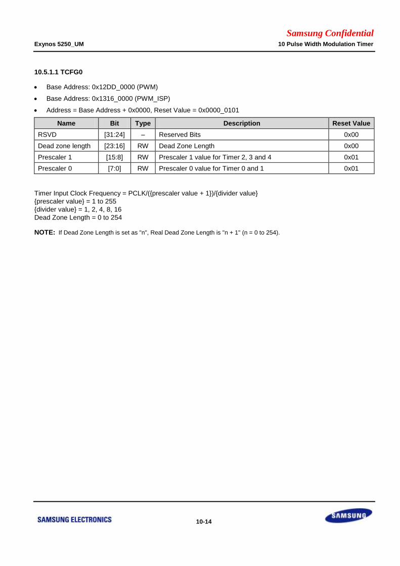
Samsung Confidential Exynos 5250_UM 10 Pulse Width Modulation Timer
10-14
10.5.1.1 TCFG0
Base Address: 0x12DD_0000 (PWM)
Base Address: 0x1316_0000 (PWM_ISP)
Address = Base Address + 0x0000, Reset Value = 0x0000_0101
Name Bit Type Description Reset Value
RSVD [31:24] – Reserved Bits 0x00
Dead zone length [23:16] RW Dead Zone Length 0x00
Prescaler 1 [15:8] RW Prescaler 1 value for Timer 2, 3 and 4 0x01
Prescaler 0 [7:0] RW Prescaler 0 value for Timer 0 and 1 0x01
Timer Input Clock Frequency = PCLK/({prescaler value + 1})/{divider value}
{prescaler value} = 1 to 255
{divider value} = 1, 2, 4, 8, 16
Dead Zone Length = 0 to 254
NOTE: If Dead Zone Length is set as "n", Real Dead Zone Length is "n + 1" (n = 0 to 254).
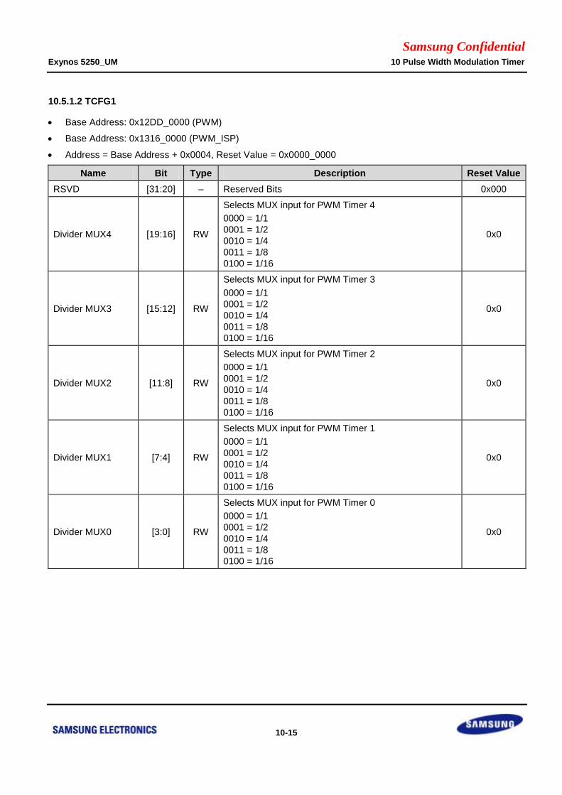
Samsung Confidential Exynos 5250_UM 10 Pulse Width Modulation Timer
10-15
10.5.1.2 TCFG1
Base Address: 0x12DD_0000 (PWM)
Base Address: 0x1316_0000 (PWM_ISP)
Address = Base Address + 0x0004, Reset Value = 0x0000_0000
Name Bit Type Description Reset Value
RSVD [31:20] – Reserved Bits 0x000
Divider MUX4 [19:16] RW
Selects MUX input for PWM Timer 4
0000 = 1/1
0001 = 1/2
0010 = 1/4
0011 = 1/8
0100 = 1/16
0x0
Divider MUX3 [15:12] RW
Selects MUX input for PWM Timer 3
0000 = 1/1
0001 = 1/2
0010 = 1/4
0011 = 1/8
0100 = 1/16
0x0
Divider MUX2 [11:8] RW
Selects MUX input for PWM Timer 2
0000 = 1/1
0001 = 1/2
0010 = 1/4
0011 = 1/8
0100 = 1/16
0x0
Divider MUX1 [7:4] RW
Selects MUX input for PWM Timer 1
0000 = 1/1
0001 = 1/2
0010 = 1/4
0011 = 1/8
0100 = 1/16
0x0
Divider MUX0 [3:0] RW
Selects MUX input for PWM Timer 0
0000 = 1/1
0001 = 1/2
0010 = 1/4
0011 = 1/8
0100 = 1/16
0x0

Samsung Confidential Exynos 5250_UM 10 Pulse Width Modulation Timer
10-16
10.5.1.3 TCON
Base Address: 0x12DD_0000 (PWM)
Base Address: 0x1316_0000 (PWM_ISP)
Address = Base Address + 0x0008, Reset Value = 0x0000_0000
Name Bit Type Description Reset Value
RSVD [31:23] – Reserved Bits 0x000
Timer 4 auto
reload on/off [22] RW
0 = One-Shot
1 = Interval Mode (Auto-Reload) 0x0
Timer 4 manual
update [21] RW
0 = No Operation
1 = Updates TCNTB4 0x0
Timer 4 start/stop [20] RW 0 = Stops
1 = Starts Timer 4 0x0
Timer 3 auto
reload on/off [19] RW
0 = One-Shot
1 = Interval Mode (Auto-Reload) 0x0
Timer 3 output
inverter on/off [18] RW
0 = Inverter Off
1 = TOUT_3 Inverter-On 0x0
Timer 3 manual
update [17] RW
0 = No Operation
1 = Updates TCNTB3 0x0
Timer 3 start/stop [16] RW 0 = Stops
1 = Starts Timer 3 0x0
Timer 2 auto
reload on/off [15] RW
0 = One-Shot
1 = Interval Mode (Auto-Reload) 0x0
Timer 2 output
inverter on/off [14] RW
0 = Inverter Off
1 = TOUT_2 Inverter-On 0x0
Timer 2 manual
update [13] RW
0 = No Operation
1 = Updates TCNTB2,TCMPB2 0x0
Timer 2 start/stop [12] RW 0 = Stops
1 = Starts Timer 2 0x0
Timer 1 auto
reload on/off [11] RW
0 = One-Shot
1 = Interval Mode (Auto-Reload) 0x0
Timer 1 output
inverter on/off [10] RW
0 = Inverter Off
1 = TOUT_1 Inverter-On 0x0
Timer 1 manual
update [9] RW
0 = No Operation
1 = Updates TCNTB1, TCMPB1 0x0
Timer 1 start/stop [8] RW 0 = Stops
1 = Starts Timer 1 0x0
Reserved [7:5] RW Reserved Bits 0x0
Dead zone
enable/disable [4] RW Dead Zone Generator Enable/Disable 0x0
Timer 0 auto
reload on/off [3] RW
0 = One-Shot
1 = Interval Mode (Auto-Reload) 0x0
Timer 0 output [2] RW 0 = Inverter Off 0x0
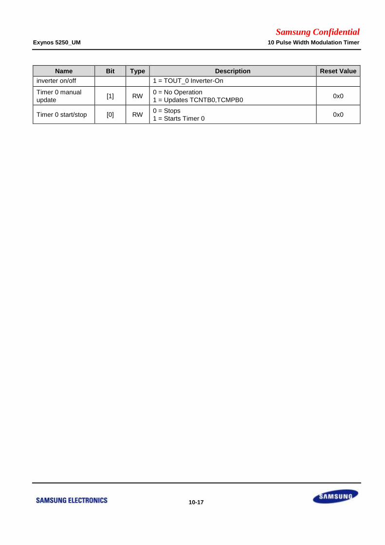
Samsung Confidential Exynos 5250_UM 10 Pulse Width Modulation Timer
10-17
Name Bit Type Description Reset Value
inverter on/off 1 = TOUT_0 Inverter-On
Timer 0 manual
update [1] RW
0 = No Operation
1 = Updates TCNTB0,TCMPB0 0x0
Timer 0 start/stop [0] RW 0 = Stops
1 = Starts Timer 0 0x0
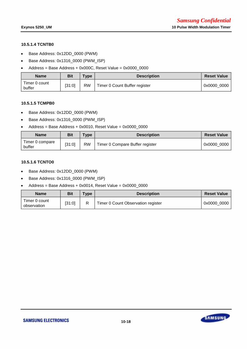
Samsung Confidential Exynos 5250_UM 10 Pulse Width Modulation Timer
10-18
10.5.1.4 TCNTB0
Base Address: 0x12DD_0000 (PWM)
Base Address: 0x1316_0000 (PWM_ISP)
Address = Base Address + 0x000C, Reset Value = 0x0000_0000
Name Bit Type Description Reset Value
Timer 0 count
buffer [31:0] RW Timer 0 Count Buffer register 0x0000_0000
10.5.1.5 TCMPB0
Base Address: 0x12DD_0000 (PWM)
Base Address: 0x1316_0000 (PWM_ISP)
Address = Base Address + 0x0010, Reset Value = 0x0000_0000
Name Bit Type Description Reset Value
Timer 0 compare
buffer [31:0] RW Timer 0 Compare Buffer register 0x0000_0000
10.5.1.6 TCNTO0
Base Address: 0x12DD_0000 (PWM)
Base Address: 0x1316_0000 (PWM_ISP)
Address = Base Address + 0x0014, Reset Value = 0x0000_0000
Name Bit Type Description Reset Value
Timer 0 count
observation [31:0] R Timer 0 Count Observation register 0x0000_0000

Samsung Confidential Exynos 5250_UM 10 Pulse Width Modulation Timer
10-19
10.5.1.7 TCNTB1
Base Address: 0x12DD_0000 (PWM)
Base Address: 0x1316_0000 (PWM_ISP)
Address = Base Address + 0x0018, Reset Value = 0x0000_0000
Name Bit Type Description Reset Value
Timer 1 count
buffer [31:0] RW Timer 1 Count Buffer register 0x0000_0000
10.5.1.8 TCMPB1
Base Address: 0x12DD_0000 (PWM)
Base Address: 0x1316_0000 (PWM_ISP)
Address = Base Address + 0x001C, Reset Value = 0x0000_0000
Name Bit Type Description Reset Value
Timer 1 compare
buffer [31:0] RW Timer 1 Compare Buffer register 0x0000_0000
10.5.1.9 TCNTO1
Base Address: 0x12DD_0000 (PWM)
Base Address: 0x1316_0000 (PWM_ISP)
Address = Base Address + 0x0020, Reset Value = 0x0000_0000
Name Bit Type Description Reset Value
Timer 1 count
observation [31:0] R Timer 1 Count Observation register 0x0000_0000

Samsung Confidential Exynos 5250_UM 10 Pulse Width Modulation Timer
10-20
10.5.1.10 TCNTB2
Base Address: 0x12DD_0000 (PWM)
Base Address: 0x1316_0000 (PWM_ISP)
Address = Base Address + 0x0024, Reset Value = 0x0000_0000
Name Bit Type Description Reset Value
Timer 2 count
buffer [31:0] RW Timer 2 Count Buffer register 0x0000_0000
10.5.1.11 TCMPB2
Base Address: 0x12DD_0000 (PWM)
Base Address: 0x1316_0000 (PWM_ISP)
Address = Base Address + 0x0028, Reset Value = 0x0000_0000
Name Bit Type Description Reset Value
Timer 2 compare
buffer [31:0] RW Timer 2 Compare Buffer register 0x0000_0000
10.5.1.12 TCNTO2
Base Address: 0x12DD_0000 (PWM)
Base Address: 0x1316_0000 (PWM_ISP)
Address = Base Address + 0x002C, Reset Value = 0x0000_0000
Name Bit Type Description Reset Value
Timer 2 count
observation [31:0] R Timer 2 Count Observation register 0x0000_0000

Samsung Confidential Exynos 5250_UM 10 Pulse Width Modulation Timer
10-21
10.5.1.13 TCNTB3
Base Address: 0x12DD_0000 (PWM)
Base Address: 0x1316_0000 (PWM_ISP)
Address = Base Address + 0x0030, Reset Value = 0x0000_0000
Name Bit Type Description Reset Value
Timer 3 count
buffer [31:0] RW Timer 3 Count Buffer register 0x0000_0000
10.5.1.14 TCMPB3
Base Address: 0x12DD_0000 (PWM)
Base Address: 0x1316_0000 (PWM_ISP)
Address = Base Address + 0x0034, Reset Value = 0x0000_0000
Name Bit Type Description Reset Value
Timer 3 compare
buffer [31:0] RW Timer 3 Compare Buffer register 0x0000_0000
10.5.1.15 TCNTO3
Base Address: 0x12DD_0000 (PWM)
Base Address: 0x1316_0000 (PWM_ISP)
Address = Base Address + 0x0038, Reset Value = 0x0000_0000
Name Bit Type Description Reset Value
Timer 3 count
observation [31:0] R Timer 3 Count Observation register 0x0000_0000

Samsung Confidential Exynos 5250_UM 10 Pulse Width Modulation Timer
10-22
10.5.1.16 TCNTB4
Base Address: 0x12DD_0000 (PWM)
Base Address: 0x1316_0000 (PWM_ISP)
Address = Base Address + 0x003C, Reset Value = 0x0000_0000
Name Bit Type Description Reset Value
Timer 4 count
buffer [31:0] RW Timer 4 Count Buffer register 0x0000_0000
10.5.1.17 TCNTO4
Base Address: 0x12DD_0000 (PWM)
Base Address: 0x1316_0000 (PWM_ISP)
Address = Base Address + 0x0040, Reset Value = 0x0000_0000
Name Bit Type Description Reset Value
Timer 4 count
observation [31:0] R Timer 4 Count Observation register 0x0000_0000
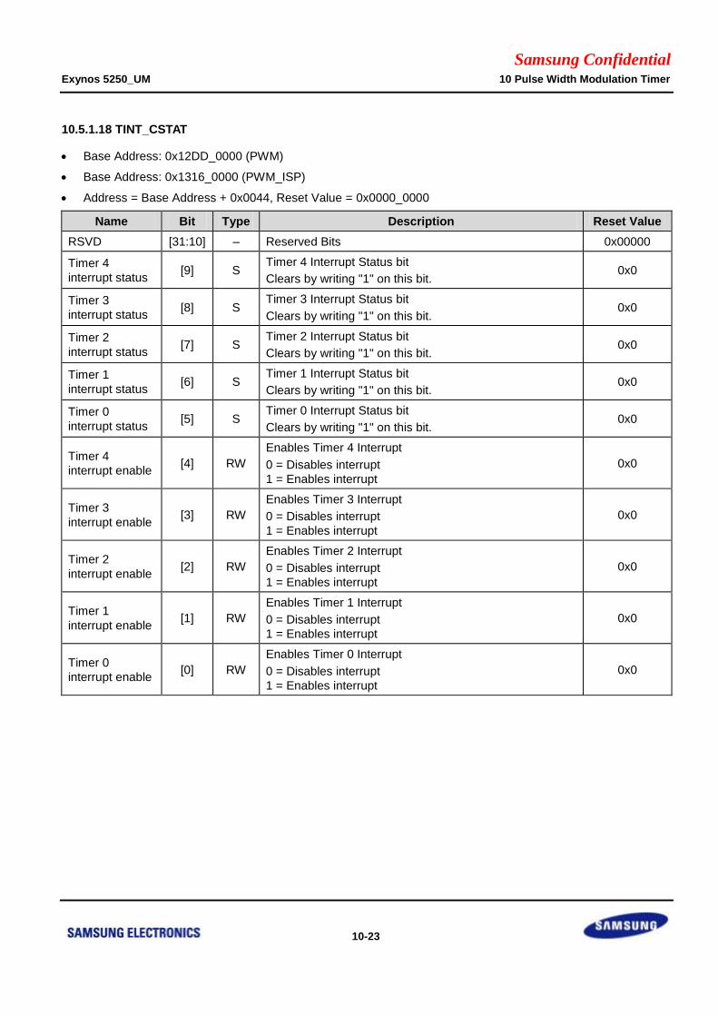
Samsung Confidential Exynos 5250_UM 10 Pulse Width Modulation Timer
10-23
10.5.1.18 TINT_CSTAT
Base Address: 0x12DD_0000 (PWM)
Base Address: 0x1316_0000 (PWM_ISP)
Address = Base Address + 0x0044, Reset Value = 0x0000_0000
Name Bit Type Description Reset Value
RSVD [31:10] – Reserved Bits 0x00000
Timer 4
interrupt status [9] S
Timer 4 Interrupt Status bit
Clears by writing "1" on this bit. 0x0
Timer 3
interrupt status [8] S
Timer 3 Interrupt Status bit
Clears by writing "1" on this bit. 0x0
Timer 2
interrupt status [7] S
Timer 2 Interrupt Status bit
Clears by writing "1" on this bit. 0x0
Timer 1
interrupt status [6] S
Timer 1 Interrupt Status bit
Clears by writing "1" on this bit. 0x0
Timer 0
interrupt status [5] S
Timer 0 Interrupt Status bit
Clears by writing "1" on this bit. 0x0
Timer 4
interrupt enable [4] RW
Enables Timer 4 Interrupt
0 = Disables interrupt
1 = Enables interrupt
0x0
Timer 3
interrupt enable [3] RW
Enables Timer 3 Interrupt
0 = Disables interrupt
1 = Enables interrupt
0x0
Timer 2
interrupt enable [2] RW
Enables Timer 2 Interrupt
0 = Disables interrupt
1 = Enables interrupt
0x0
Timer 1
interrupt enable [1] RW
Enables Timer 1 Interrupt
0 = Disables interrupt
1 = Enables interrupt
0x0
Timer 0
interrupt enable [0] RW
Enables Timer 0 Interrupt
0 = Disables interrupt
1 = Enables interrupt
0x0
Samsung Confidential Exynos 5250_UM 11 Watchdog Timer
11-1
11 Watchdog Timer
11.1 Overview
Watchdog Timer (WDT) in Exynos 5250 is a timing device. You can use this device to resume the controller
operation after malfunctioning due to noise and system errors. You can use WDT as a normal 16-bit interval timer
to request interrupt service. WDT generates the reset signal.
Both of WDT and PWM timer are normal generate internal interrupts for the ARM subsystem. The difference
between WDT and PWM timer is that only WDT generates the reset signal. (Refer to PWM Timer chapter for more
information on PWM Timer.)
11.2 Features
The features of WDT are:
Supports normal interval timer mode with interrupt request.
Activates internal reset signal if the timer count value reaches 0 (time-out).
Supports level-triggered interrupt mechanism

Samsung Confidential Exynos 5250_UM 11 Watchdog Timer
11-2
11.3 Functional Description
This section includes:
WDT Operation
WTDAT and WTCNT
WDT Start
Consideration of debugging environment
11.3.1 WDT Operation
WDT timer uses PCLK as its source clock. The PCLK frequency is prescaled to generate the corresponding WDT
clock and it divides the resulting frequency again.
Figure 11-1 illustrates the functional block diagram of the WDT.
Figure 11-1 Watchdog Timer Block Diagram
The Watchdog Timer Control (WTCON) specifies the prescaler value and frequency division factor. The valid
prescaler values range from 0 to 28-1. You can select the frequency division factor as: 16, 32, 64, or 128.
Use this equation to calculate WDT clock frequency and the duration of each timer clock cycle:
t_watchdog = 1/(PCLK/(Prescaler value + 1)/Division_factor)
Reset Signal GeneratorWTCNT
(Down Counter)PCLK
WTCON[4:3]
WTDAT
RESET
1/16
1/32
1/64
1/128
8-bit Prescaler
WTCON[15:8] WTCON[2] WTCON[0]
Interrupt
MUX

Samsung Confidential Exynos 5250_UM 11 Watchdog Timer
11-3
11.3.2 WTDAT and WTCNT
After you enable the WDT, you cannot reload the value of the Watchdog Timer Data (WTDAT) register
automatically into the Watchdog Timer Counter (WTCNT) register. Therefore, you must write an initial value to the
WTCN register before WDT starts. .
11.3.3 WDT Start
To start WDT, set WTCON[0] and WTCON[5] as 1.
11.3.4 Consideration of Debugging Environment
WDT must not operate when the Exynos 5250 is in debug mode that uses Embedded ICE.
WDT determines if Exynos 5250 is currently in the debug mode from the CPU core signal (DBGACK signal). After
the DBGACK signal is asserted, it does not activate the reset output of WDT as WDT expires.
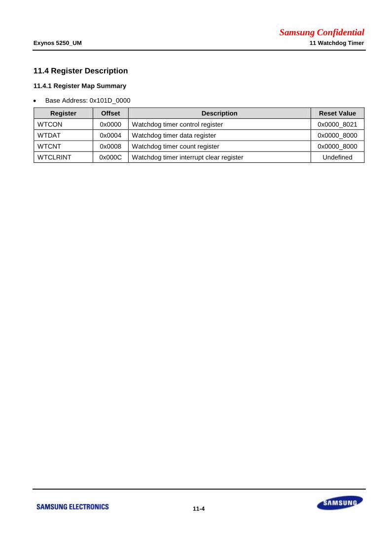
Samsung Confidential Exynos 5250_UM 11 Watchdog Timer
11-4
11.4 Register Description
11.4.1 Register Map Summary
Base Address: 0x101D_0000
Register Offset Description Reset Value
WTCON 0x0000 Watchdog timer control register 0x0000_8021
WTDAT 0x0004 Watchdog timer data register 0x0000_8000
WTCNT 0x0008 Watchdog timer count register 0x0000_8000
WTCLRINT 0x000C Watchdog timer interrupt clear register Undefined
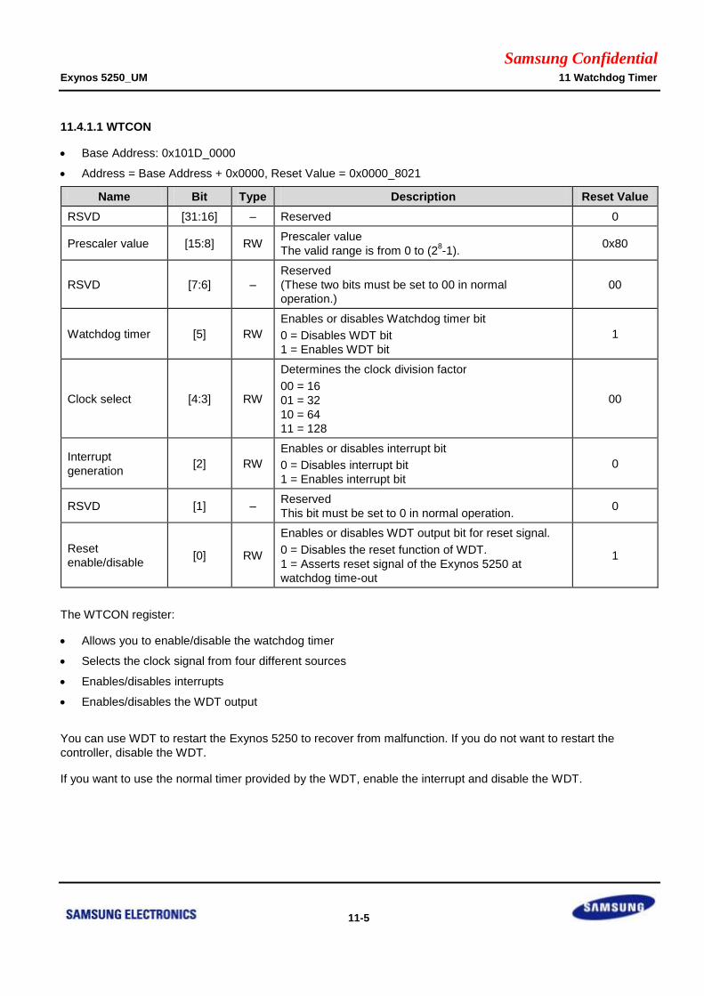
Samsung Confidential Exynos 5250_UM 11 Watchdog Timer
11-5
11.4.1.1 WTCON
Base Address: 0x101D_0000
Address = Base Address + 0x0000, Reset Value = 0x0000_8021
Name Bit Type Description Reset Value
RSVD [31:16] – Reserved 0
Prescaler value [15:8] RW Prescaler value
The valid range is from 0 to (28-1).
0x80
RSVD [7:6] –
Reserved
(These two bits must be set to 00 in normal
operation.)
00
Watchdog timer [5] RW
Enables or disables Watchdog timer bit
0 = Disables WDT bit
1 = Enables WDT bit
1
Clock select [4:3] RW
Determines the clock division factor
00 = 16
01 = 32
10 = 64
11 = 128
00
Interrupt
generation [2] RW
Enables or disables interrupt bit
0 = Disables interrupt bit
1 = Enables interrupt bit
0
RSVD [1] – Reserved
This bit must be set to 0 in normal operation. 0
Reset
enable/disable [0] RW
Enables or disables WDT output bit for reset signal.
0 = Disables the reset function of WDT.
1 = Asserts reset signal of the Exynos 5250 at
watchdog time-out
1
The WTCON register:
Allows you to enable/disable the watchdog timer
Selects the clock signal from four different sources
Enables/disables interrupts
Enables/disables the WDT output
You can use WDT to restart the Exynos 5250 to recover from malfunction. If you do not want to restart the
controller, disable the WDT.
If you want to use the normal timer provided by the WDT, enable the interrupt and disable the WDT.
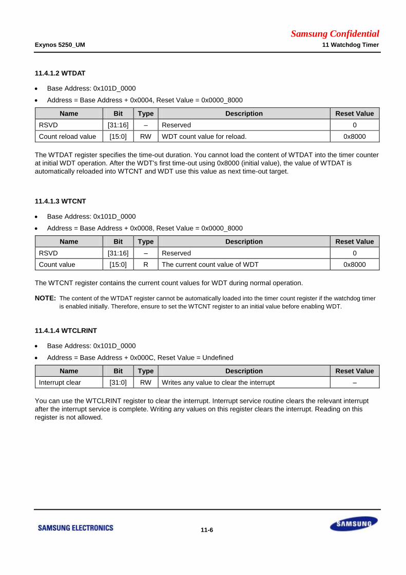
Samsung Confidential Exynos 5250_UM 11 Watchdog Timer
11-6
11.4.1.2 WTDAT
Base Address: 0x101D_0000
Address = Base Address + 0x0004, Reset Value = 0x0000_8000
Name Bit Type Description Reset Value
RSVD [31:16] – Reserved 0
Count reload value [15:0] RW WDT count value for reload. 0x8000
The WTDAT register specifies the time-out duration. You cannot load the content of WTDAT into the timer counter
at initial WDT operation. After the WDT's first time-out using 0x8000 (initial value), the value of WTDAT is
automatically reloaded into WTCNT and WDT use this value as next time-out target.
11.4.1.3 WTCNT
Base Address: 0x101D_0000
Address = Base Address + 0x0008, Reset Value = 0x0000_8000
Name Bit Type Description Reset Value
RSVD [31:16] – Reserved 0
Count value [15:0] R The current count value of WDT 0x8000
The WTCNT register contains the current count values for WDT during normal operation.
NOTE: The content of the WTDAT register cannot be automatically loaded into the timer count register if the watchdog timer
is enabled initially. Therefore, ensure to set the WTCNT register to an initial value before enabling WDT.
11.4.1.4 WTCLRINT
Base Address: 0x101D_0000
Address = Base Address + 0x000C, Reset Value = Undefined
Name Bit Type Description Reset Value
Interrupt clear [31:0] RW Writes any value to clear the interrupt –
You can use the WTCLRINT register to clear the interrupt. Interrupt service routine clears the relevant interrupt
after the interrupt service is complete. Writing any values on this register clears the interrupt. Reading on this
register is not allowed.
Samsung Confidential Exynos 5250_UM 12 Universal Asynchronous Receiver and Transmitter
12-1
12 Universal Asynchronous Receiver and Transmitter
12.1 Overview
The Universal Asynchronous Receiver and Transmitter (UART) in Exynos 5250 provide:
Four independent channels with asynchronous and serial input/output ports for general purpose (Channel 0 to 3),
and One channel in ISP (ISP-UART Channel 0)
All ports operate in an Interrupt-based or a DMA-based mode. The UART generates an interrupt or a DMA
request to transfer data to and from the CPU and the UART.
The UART supports bit rates up to 3 Mbps. Each UART channel contains two FIFOs to receive and transmit data:
256 bytes in Channel 0
64 bytes in Channel 1 and ISP-UART Channel 0,
16 bytes in Channel 2 and Channel 3
UART includes programmable Baud Rates, Infrared (IR) Transmitter/Receiver, one or two Stop Bit Insertion, 5-bit,
6-bit, 7-bit, or 8-bit Data Width and Parity Checking.
Each UART contains a Baud-rate generator, a Transmitter, a Receiver and a Control Unit. The Baud-rate
generator uses SCLK_UART. The Transmitter and the Receiver contain FIFOs and data shifters. The data that is
transmitted is written to Tx FIFO, and copied to the transmit shifter. The data is then shifted out by the transmit
data pin (TxDn). The received data is shifted from the Receive Data Pin (RxDn), and copied to Rx FIFO from the
shifter.
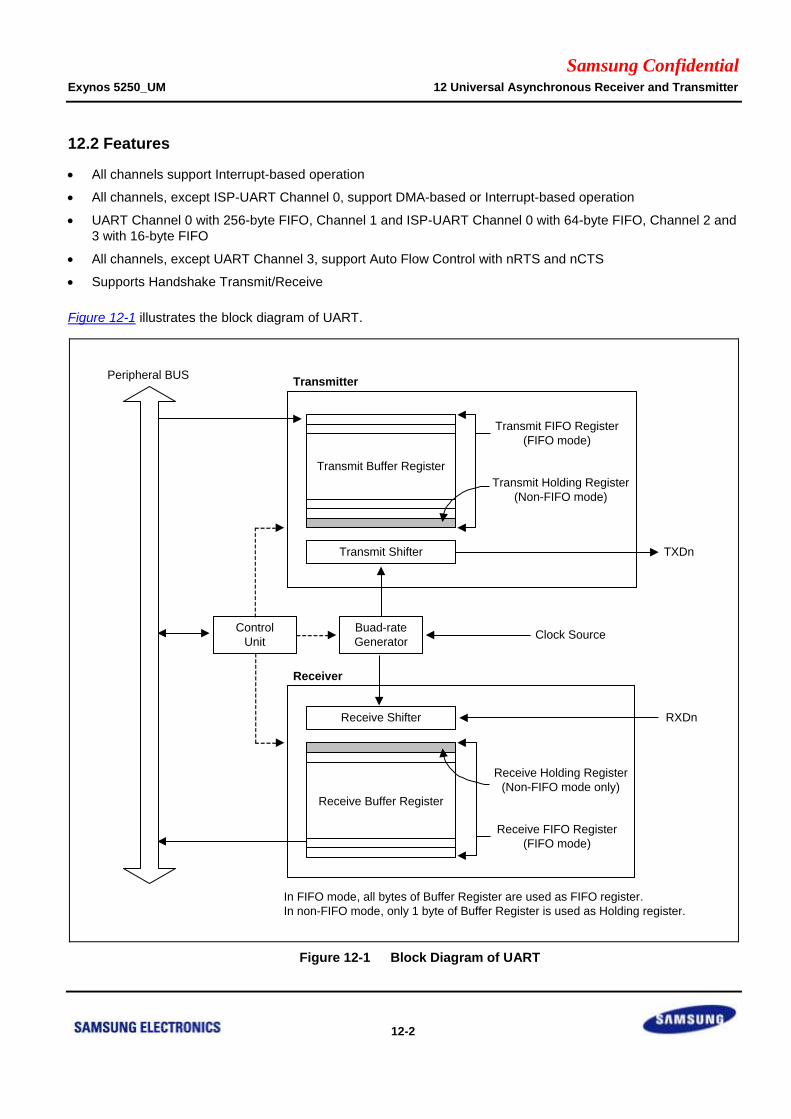
Samsung Confidential Exynos 5250_UM 12 Universal Asynchronous Receiver and Transmitter
12-2
12.2 Features
All channels support Interrupt-based operation
All channels, except ISP-UART Channel 0, support DMA-based or Interrupt-based operation
UART Channel 0 with 256-byte FIFO, Channel 1 and ISP-UART Channel 0 with 64-byte FIFO, Channel 2 and
3 with 16-byte FIFO
All channels, except UART Channel 3, support Auto Flow Control with nRTS and nCTS
Supports Handshake Transmit/Receive
Figure 12-1 illustrates the block diagram of UART.
Figure 12-1 Block Diagram of UART
Buad-rate
Generator
Control
Unit
Transmitter
Receiver
Peripheral BUS
TXDn
Clock Source
RXDn
Transmit FIFO Register
(FIFO mode)
Transmit Holding Register
(Non-FIFO mode)
Receive FIFO Register
(FIFO mode)
Receive Holding Register
(Non-FIFO mode only)
In FIFO mode, all bytes of Buffer Register are used as FIFO register.
In non-FIFO mode, only 1 byte of Buffer Register is used as Holding register.
Transmit Shifter
Transmit Buffer Register
Receive Shifter
Receive Buffer Register
Samsung Confidential Exynos 5250_UM 12 Universal Asynchronous Receiver and Transmitter
12-3
12.3 UART Description
This section describes UART operations, such as Data Transmission, Data Reception, Interrupt Generation,
Baud-rate Generation, Loop-back mode, Infrared modes, and Auto Flow Control.
12.3.1 Data Transmission
The data frame for transmission is programmable. It consists of a start bit, five to eight data bits, an optional parity
bit, and one to two stop bits, specified by the line control register (ULCONn). The transmitter can also produce a
break condition that forces the serial output to logic 0 state, for one frame transmission time. This block transmits
the break signals, after the present transmission word is transmitted completely. After the break signal
transmission, the transmitter continuously transmits data to Tx FIFO (Tx holding register, in case of Non-FIFO
mode).
12.3.2 Data Reception
Similar to data transmission, the data frame for reception is also programmable. It consists of a start bit, five to
eight data bits, an optional parity bit, and one to two stop bits in the Line Control Register (ULCONn). The receiver
detects Overrun Error, Parity Error, Frame Error and Break Condition. Each of this error sets an error flag.
Overrun Error indicates that new data has overwritten the old data before it was read
Parity Error indicates that the receiver has detected an unexpected parity condition
Frame Error indicates that the received data does not have a valid stop bit
Break Condition indicates that the RxDn input is held in the logic 0 state for more than one frame transmission
time
Receive time-out condition occurs when the Rx FIFO is not empty in the FIFO mode and no more data is received
during the frame time specified in UCON.
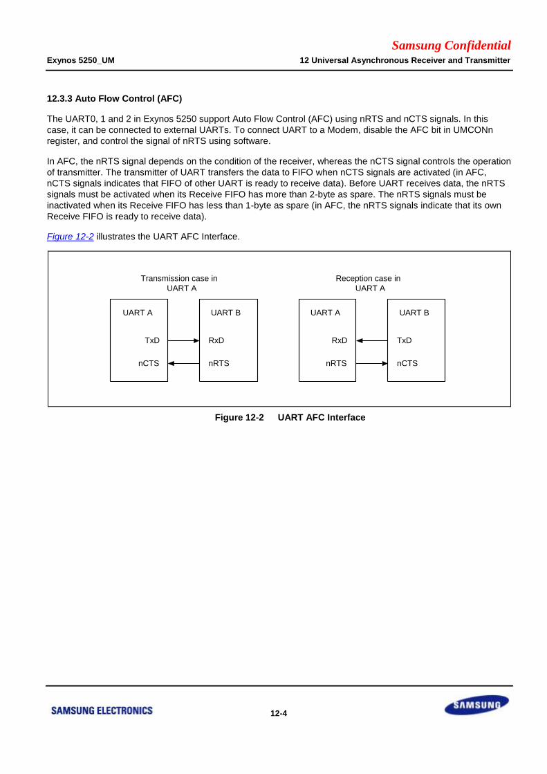
Samsung Confidential Exynos 5250_UM 12 Universal Asynchronous Receiver and Transmitter
12-4
12.3.3 Auto Flow Control (AFC)
The UART0, 1 and 2 in Exynos 5250 support Auto Flow Control (AFC) using nRTS and nCTS signals. In this
case, it can be connected to external UARTs. To connect UART to a Modem, disable the AFC bit in UMCONn
register, and control the signal of nRTS using software.
In AFC, the nRTS signal depends on the condition of the receiver, whereas the nCTS signal controls the operation
of transmitter. The transmitter of UART transfers the data to FIFO when nCTS signals are activated (in AFC,
nCTS signals indicates that FIFO of other UART is ready to receive data). Before UART receives data, the nRTS
signals must be activated when its Receive FIFO has more than 2-byte as spare. The nRTS signals must be
inactivated when its Receive FIFO has less than 1-byte as spare (in AFC, the nRTS signals indicate that its own
Receive FIFO is ready to receive data).
Figure 12-2 illustrates the UART AFC Interface.
Figure 12-2 UART AFC Interface
RxD
nRTS
UART A
TxD
nCTS
UART B
TxD
nCTS
UART A
RxD
nRTS
UART B
Transmission case in
UART A
Reception case in
UART A
Samsung Confidential Exynos 5250_UM 12 Universal Asynchronous Receiver and Transmitter
12-5
12.3.4 Non Auto-Flow Control (Controlling nRTS and nCTS by Software)
12.3.4.1 Rx Operation with FIFO
This procedures describes the Rx Operation with FIFO:
1. Select the transmit mode (Interrupt or DMA mode)
2. Check the value of Rx FIFO count in UFSTATn register. When the value is less than 16, you must set the
value of UMCONn[0] to "1" (activate nRTS). However, when the value is equal to or greater than 16,
you must set the value to "0" (inactivate nRTS).
3. Repeat the Step 2
12.3.4.2 Tx Operation with FIFO
This procedure describes the Tx Operation with FIFO:
1. Select the transmit mode (Interrupt or DMA mode)
2. Check the value of UMSTATn[0]. When the value is "1" (activate nCTS), you must write data to Tx FIFO
register
3. Repeat the Step 2
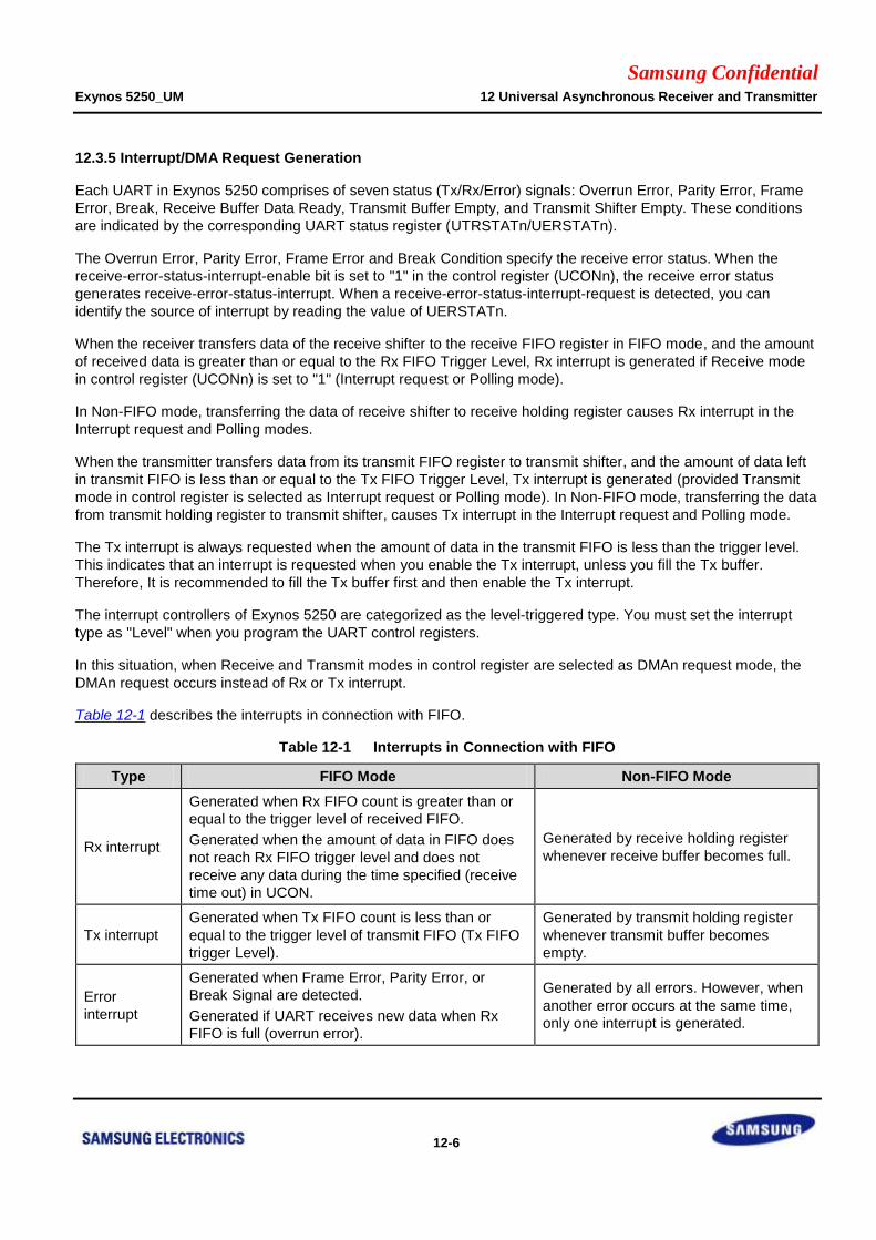
Samsung Confidential Exynos 5250_UM 12 Universal Asynchronous Receiver and Transmitter
12-6
12.3.5 Interrupt/DMA Request Generation
Each UART in Exynos 5250 comprises of seven status (Tx/Rx/Error) signals: Overrun Error, Parity Error, Frame
Error, Break, Receive Buffer Data Ready, Transmit Buffer Empty, and Transmit Shifter Empty. These conditions
are indicated by the corresponding UART status register (UTRSTATn/UERSTATn).
The Overrun Error, Parity Error, Frame Error and Break Condition specify the receive error status. When the
receive-error-status-interrupt-enable bit is set to "1" in the control register (UCONn), the receive error status
generates receive-error-status-interrupt. When a receive-error-status-interrupt-request is detected, you can
identify the source of interrupt by reading the value of UERSTATn.
When the receiver transfers data of the receive shifter to the receive FIFO register in FIFO mode, and the amount
of received data is greater than or equal to the Rx FIFO Trigger Level, Rx interrupt is generated if Receive mode
in control register (UCONn) is set to "1" (Interrupt request or Polling mode).
In Non-FIFO mode, transferring the data of receive shifter to receive holding register causes Rx interrupt in the
Interrupt request and Polling modes.
When the transmitter transfers data from its transmit FIFO register to transmit shifter, and the amount of data left
in transmit FIFO is less than or equal to the Tx FIFO Trigger Level, Tx interrupt is generated (provided Transmit
mode in control register is selected as Interrupt request or Polling mode). In Non-FIFO mode, transferring the data
from transmit holding register to transmit shifter, causes Tx interrupt in the Interrupt request and Polling mode.
The Tx interrupt is always requested when the amount of data in the transmit FIFO is less than the trigger level.
This indicates that an interrupt is requested when you enable the Tx interrupt, unless you fill the Tx buffer.
Therefore, It is recommended to fill the Tx buffer first and then enable the Tx interrupt.
The interrupt controllers of Exynos 5250 are categorized as the level-triggered type. You must set the interrupt
type as "Level" when you program the UART control registers.
In this situation, when Receive and Transmit modes in control register are selected as DMAn request mode, the
DMAn request occurs instead of Rx or Tx interrupt.
Table 12-1 describes the interrupts in connection with FIFO.
Table 12-1 Interrupts in Connection with FIFO
Type FIFO Mode Non-FIFO Mode
Rx interrupt
Generated when Rx FIFO count is greater than or
equal to the trigger level of received FIFO.
Generated when the amount of data in FIFO does
not reach Rx FIFO trigger level and does not
receive any data during the time specified (receive
time out) in UCON.
Generated by receive holding register
whenever receive buffer becomes full.
Tx interrupt
Generated when Tx FIFO count is less than or
equal to the trigger level of transmit FIFO (Tx FIFO
trigger Level).
Generated by transmit holding register
whenever transmit buffer becomes
empty.
Error
interrupt
Generated when Frame Error, Parity Error, or
Break Signal are detected.
Generated if UART receives new data when Rx
FIFO is full (overrun error).
Generated by all errors. However, when
another error occurs at the same time,
only one interrupt is generated.
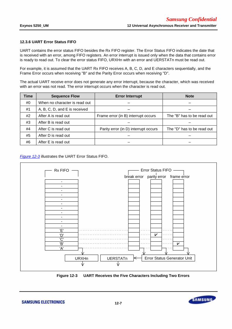
Samsung Confidential Exynos 5250_UM 12 Universal Asynchronous Receiver and Transmitter
12-7
12.3.6 UART Error Status FIFO
UART contains the error status FIFO besides the Rx FIFO register. The Error Status FIFO indicates the date that
is received with an error, among FIFO registers. An error interrupt is issued only when the data that contains error
is ready to read out. To clear the error status FIFO, URXHn with an error and UERSTATn must be read out.
For example, it is assumed that the UART Rx FIFO receives A, B, C, D, and E characters sequentially, and the
Frame Error occurs when receiving "B" and the Parity Error occurs when receiving "D".
The actual UART receive error does not generate any error interrupt, because the character, which was received
with an error was not read. The error interrupt occurs when the character is read out.
Time Sequence Flow Error Interrupt Note
#0 When no character is read out – –
#1 A, B, C, D, and E is received – –
#2 After A is read out Frame error (in B) interrupt occurs The "B" has to be read out
#3 After B is read out – –
#4 After C is read out Parity error (in D) interrupt occurs The "D" has to be read out
#5 After D is read out – –
#6 After E is read out – –
Figure 12-3 illustrates the UART Error Status FIFO.
Figure 12-3 UART Receives the Five Characters Including Two Errors
-----------
'E'
'D''C''B'
'A'
Rx FIFO
URXHn UERSTATn
break error parity error frame error
Error Status Generator Unit
Error Status FIFO
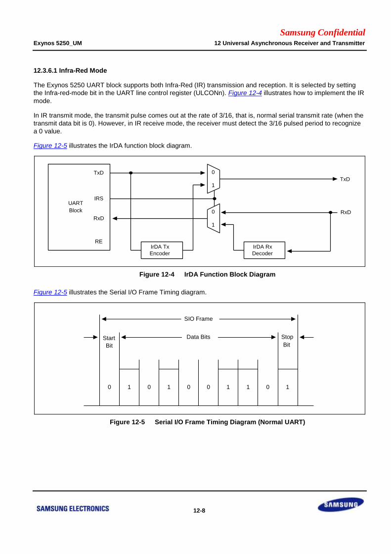
Samsung Confidential Exynos 5250_UM 12 Universal Asynchronous Receiver and Transmitter
12-8
12.3.6.1 Infra-Red Mode
The Exynos 5250 UART block supports both Infra-Red (IR) transmission and reception. It is selected by setting
the Infra-red-mode bit in the UART line control register (ULCONn). Figure 12-4 illustrates how to implement the IR
mode.
In IR transmit mode, the transmit pulse comes out at the rate of 3/16, that is, normal serial transmit rate (when the
transmit data bit is 0). However, in IR receive mode, the receiver must detect the 3/16 pulsed period to recognize
a 0 value.
Figure 12-5 illustrates the IrDA function block diagram.
Figure 12-4 IrDA Function Block Diagram
Figure 12-5 illustrates the Serial I/O Frame Timing diagram.
Figure 12-5 Serial I/O Frame Timing Diagram (Normal UART)
IrDA Tx
Encoder
0
1
0
1
IrDA Rx
Decoder
TxD
RxD
TxD
IRS
RxD
RE
UART
Block
Start
Bit
Stop
Bit
Data Bits
SIO Frame
0 1 0 1 0 0 1 1 0 1
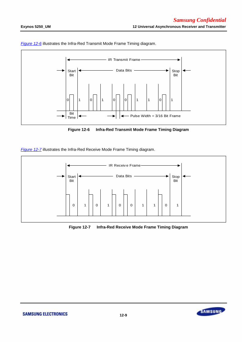
Samsung Confidential Exynos 5250_UM 12 Universal Asynchronous Receiver and Transmitter
12-9
Figure 12-6 illustrates the Infra-Red Transmit Mode Frame Timing diagram.
Figure 12-6 Infra-Red Transmit Mode Frame Timing Diagram
Figure 12-7 illustrates the Infra-Red Receive Mode Frame Timing diagram.
Figure 12-7 Infra-Red Receive Mode Frame Timing Diagram
0
Start
Bit
Stop
Bit
Data Bits
IR Transmit Frame
Bit
TimePulse Width = 3/16 Bit Frame
0 0 0 0 11111
0
Start
Bit
Stop
Bit
Data Bits
IR Receiv e Frame
0 0 0 0 11111
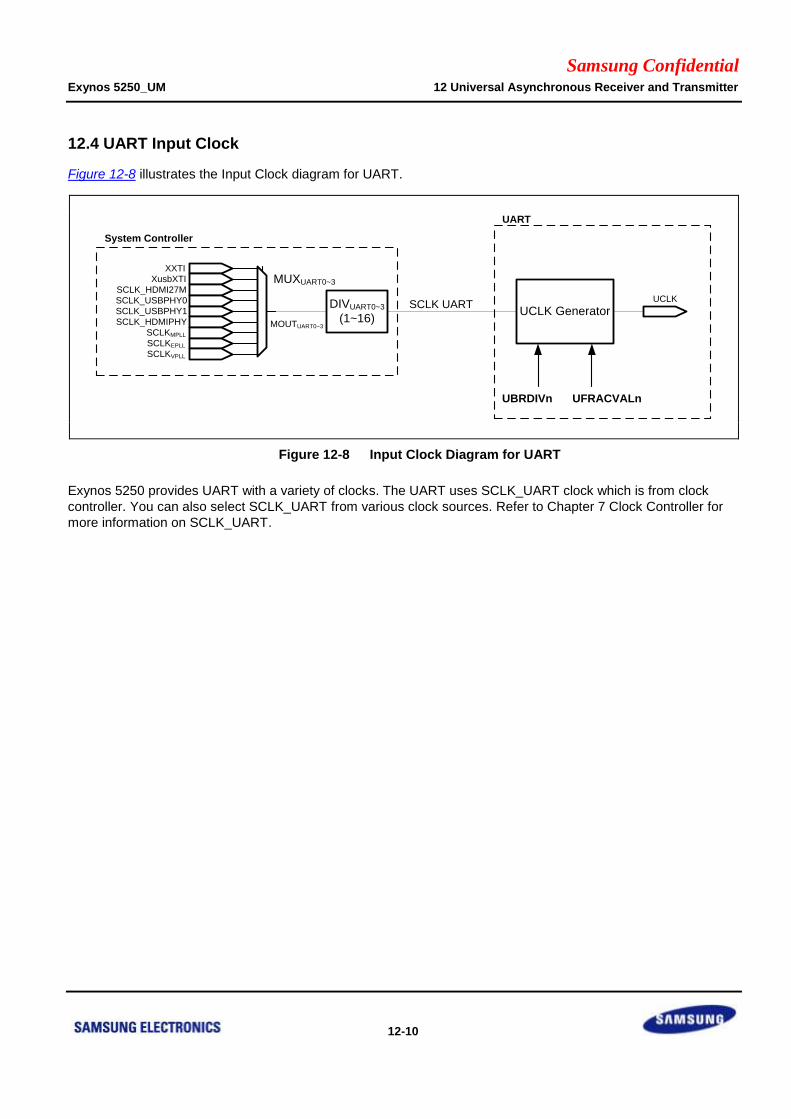
Samsung Confidential Exynos 5250_UM 12 Universal Asynchronous Receiver and Transmitter
12-10
12.4 UART Input Clock
Figure 12-8 illustrates the Input Clock diagram for UART.
System Controller
DIVUART0~3
(1~16)
MUXUART0~3
MOUTUART0~3
XXTI
XusbXTI
SCLK_HDMI27M
SCLK_USBPHY0
SCLK_USBPHY1
SCLK_HDMIPHY
SCLKMPLL
SCLKEPLL
SCLKVPLL
UCLK
UCLK Generator
UBRDIVn UFRACVALn
UART
SCLK UART
Figure 12-8 Input Clock Diagram for UART
Exynos 5250 provides UART with a variety of clocks. The UART uses SCLK_UART clock which is from clock
controller. You can also select SCLK_UART from various clock sources. Refer to Chapter 7 Clock Controller for
more information on SCLK_UART.
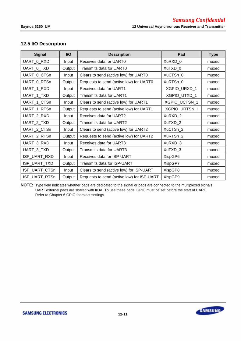
Samsung Confidential Exynos 5250_UM 12 Universal Asynchronous Receiver and Transmitter
12-11
12.5 I/O Description
Signal I/O Description Pad Type
UART_0_RXD Input Receives data for UART0 XuRXD_0 muxed
UART_0_TXD Output Transmits data for UART0 XuTXD_0 muxed
UART_0_CTSn Input Clears to send (active low) for UART0 XuCTSn_0 muxed
UART_0_RTSn Output Requests to send (active low) for UART0 XuRTSn_0 muxed
UART_1_RXD Input Receives data for UART1 XGPIO_URXD_1 muxed
UART_1_TXD Output Transmits data for UART1 XGPIO_UTXD_1 muxed
UART_1_CTSn Input Clears to send (active low) for UART1 XGPIO_UCTSN_1 muxed
UART_1_RTSn Output Requests to send (active low) for UART1 XGPIO_URTSN_! muxed
UART_2_RXD Input Receives data for UART2 XuRXD_2 muxed
UART_2_TXD Output Transmits data for UART2 XuTXD_2 muxed
UART_2_CTSn Input Clears to send (active low) for UART2 XuCTSn_2 muxed
UART_2_RTSn Output Requests to send (active low) for UART2 XuRTSn_2 muxed
UART_3_RXD Input Receives data for UART3 XuRXD_3 muxed
UART_3_TXD Output Transmits data for UART3 XuTXD_3 muxed
ISP_UART_RXD Input Receives data for ISP-UART XispGP6 muxed
ISP_UART_TXD Output Transmits data for ISP-UART XispGP7 muxed
ISP_UART_CTSn Input Clears to send (active low) for ISP-UART XispGP8 muxed
ISP_UART_RTSn Output Requests to send (active low) for ISP-UART XispGP9 muxed
NOTE: Type field indicates whether pads are dedicated to the signal or pads are connected to the multiplexed signals.
UART external pads are shared with IrDA. To use these pads, GPIO must be set before the start of UART.
Refer to Chapter 6 GPIO for exact settings.
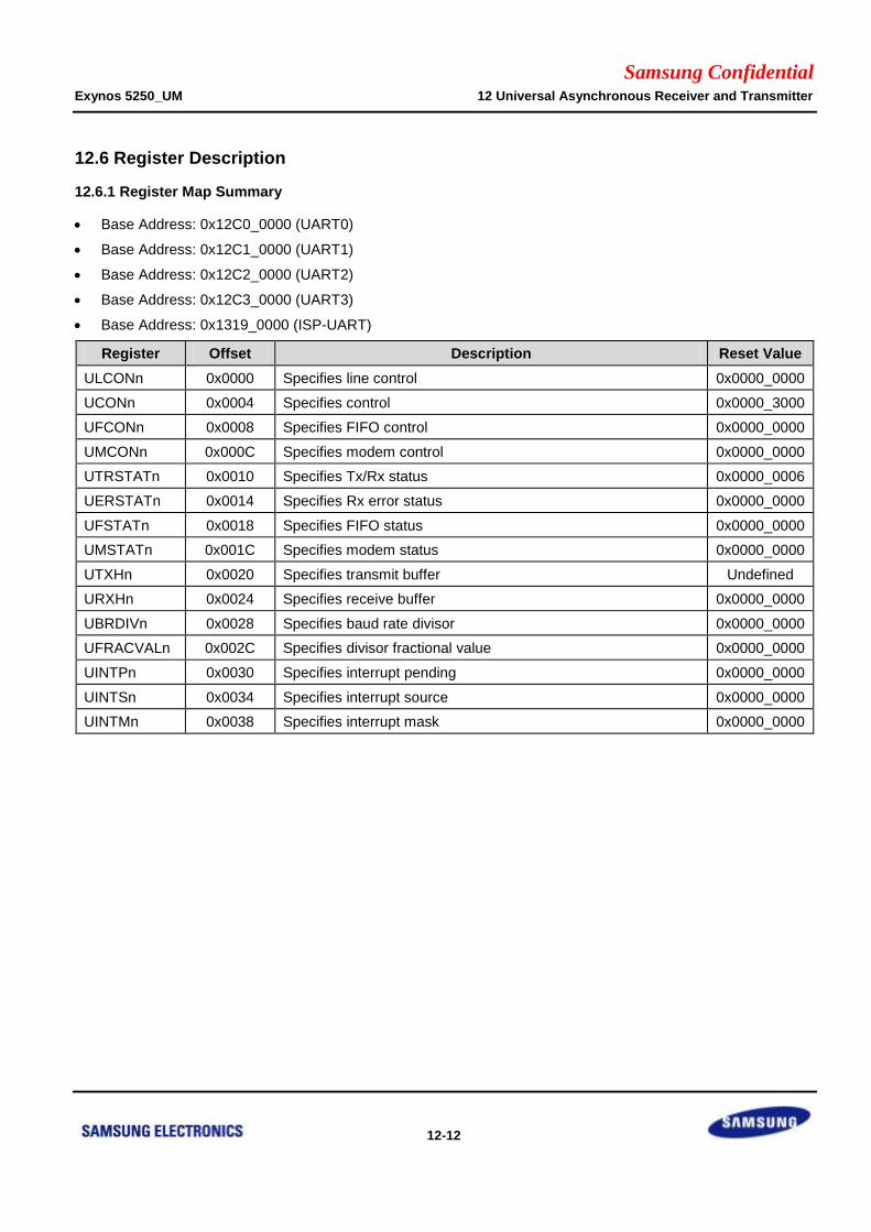
Samsung Confidential Exynos 5250_UM 12 Universal Asynchronous Receiver and Transmitter
12-12
12.6 Register Description
12.6.1 Register Map Summary
Base Address: 0x12C0_0000 (UART0)
Base Address: 0x12C1_0000 (UART1)
Base Address: 0x12C2_0000 (UART2)
Base Address: 0x12C3_0000 (UART3)
Base Address: 0x1319_0000 (ISP-UART)
Register Offset Description Reset Value
ULCONn 0x0000 Specifies line control 0x0000_0000
UCONn 0x0004 Specifies control 0x0000_3000
UFCONn 0x0008 Specifies FIFO control 0x0000_0000
UMCONn 0x000C Specifies modem control 0x0000_0000
UTRSTATn 0x0010 Specifies Tx/Rx status 0x0000_0006
UERSTATn 0x0014 Specifies Rx error status 0x0000_0000
UFSTATn 0x0018 Specifies FIFO status 0x0000_0000
UMSTATn 0x001C Specifies modem status 0x0000_0000
UTXHn 0x0020 Specifies transmit buffer Undefined
URXHn 0x0024 Specifies receive buffer 0x0000_0000
UBRDIVn 0x0028 Specifies baud rate divisor 0x0000_0000
UFRACVALn 0x002C Specifies divisor fractional value 0x0000_0000
UINTPn 0x0030 Specifies interrupt pending 0x0000_0000
UINTSn 0x0034 Specifies interrupt source 0x0000_0000
UINTMn 0x0038 Specifies interrupt mask 0x0000_0000
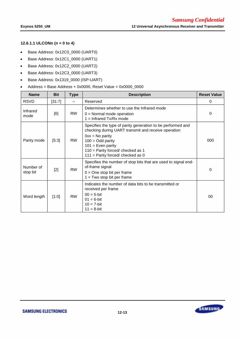
Samsung Confidential Exynos 5250_UM 12 Universal Asynchronous Receiver and Transmitter
12-13
12.6.1.1 ULCONn (n = 0 to 4)
Base Address: 0x12C0_0000 (UART0)
Base Address: 0x12C1_0000 (UART1)
Base Address: 0x12C2_0000 (UART2)
Base Address: 0x12C3_0000 (UART3)
Base Address: 0x1319_0000 (ISP-UART)
Address = Base Address + 0x0000, Reset Value = 0x0000_0000
Name Bit Type Description Reset Value
RSVD [31:7] – Reserved 0
Infrared
mode [6] RW
Determines whether to use the Infrared mode
0 = Normal mode operation
1 = Infrared Tx/Rx mode
0
Parity mode [5:3] RW
Specifies the type of parity generation to be performed and
checking during UART transmit and receive operation
0xx = No parity
100 = Odd parity
101 = Even parity
110 = Parity forced/ checked as 1
111 = Parity forced/ checked as 0
000
Number of
stop bit [2] RW
Specifies the number of stop bits that are used to signal end-
of-frame signal
0 = One stop bit per frame
1 = Two stop bit per frame
0
Word length [1:0] RW
Indicates the number of data bits to be transmitted or
received per frame
00 = 5-bit
01 = 6-bit
10 = 7-bit
11 = 8-bit
00
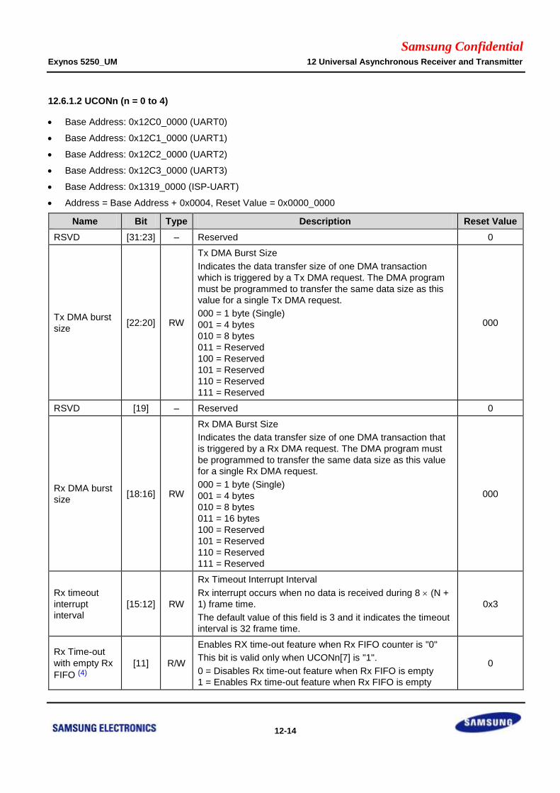
Samsung Confidential Exynos 5250_UM 12 Universal Asynchronous Receiver and Transmitter
12-14
12.6.1.2 UCONn (n = 0 to 4)
Base Address: 0x12C0_0000 (UART0)
Base Address: 0x12C1_0000 (UART1)
Base Address: 0x12C2_0000 (UART2)
Base Address: 0x12C3_0000 (UART3)
Base Address: 0x1319_0000 (ISP-UART)
Address = Base Address + 0x0004, Reset Value = 0x0000_0000
Name Bit Type Description Reset Value
RSVD [31:23] – Reserved 0
Tx DMA burst
size [22:20] RW
Tx DMA Burst Size
Indicates the data transfer size of one DMA transaction
which is triggered by a Tx DMA request. The DMA program
must be programmed to transfer the same data size as this
value for a single Tx DMA request.
000 = 1 byte (Single)
001 = 4 bytes
010 = 8 bytes
011 = Reserved
100 = Reserved
101 = Reserved
110 = Reserved
111 = Reserved
000
RSVD [19] – Reserved 0
Rx DMA burst
size [18:16] RW
Rx DMA Burst Size
Indicates the data transfer size of one DMA transaction that
is triggered by a Rx DMA request. The DMA program must
be programmed to transfer the same data size as this value
for a single Rx DMA request.
000 = 1 byte (Single)
001 = 4 bytes
010 = 8 bytes
011 = 16 bytes
100 = Reserved
101 = Reserved
110 = Reserved
111 = Reserved
000
Rx timeout
interrupt
interval
[15:12] RW
Rx Timeout Interrupt Interval
Rx interrupt occurs when no data is received during 8 (N +
1) frame time.
The default value of this field is 3 and it indicates the timeout
interval is 32 frame time.
0x3
Rx Time-out
with empty Rx
FIFO (4)
[11] R/W
Enables RX time-out feature when Rx FIFO counter is "0"
This bit is valid only when UCONn[7] is "1".
0 = Disables Rx time-out feature when Rx FIFO is empty
1 = Enables Rx time-out feature when Rx FIFO is empty
0

Samsung Confidential Exynos 5250_UM 12 Universal Asynchronous Receiver and Transmitter
12-15
Name Bit Type Description Reset Value
Rx Time-out
DMA suspend
enable
[10] R/W
Enables Rx DMA FSM to suspend when Rx Time-out occurs
0 = Disables suspending Rx DMA FSM
1 = Enables suspending Rx DMA FSM
0
Tx Interrupt
Type [9] RW
Interrupt request type(2)
0 = Pulse (interrupt is requested when the Tx buffer is empty
in the Non-FIFO mode, or when it reaches Tx FIFO Trigger
Level in the FIFO mode)
1 = Level (interrupt is requested when Tx buffer is empty in
the Non-FIFO mode, or when it reaches Tx FIFO Trigger
Level in the FIFO mode)
0
Rx Interrupt
Type [8] RW
Interrupt request type (2)
0 = Pulse (interrupt is requested when instant Rx buffer
receives data in the Non-FIFO mode, or when it reaches Rx
FIFO Trigger Level in the FIFO mode)
1 = Level (interrupt is requested when Rx buffer receives
data in the Non-FIFO mode, or when it reaches Rx FIFO
Trigger Level in the FIFO mode)
0
Rx Time Out
Enable [7] RW
Enables/Disables Rx time-out interrupts when UART FIFO is
enabled. The interrupt is a receive interrupt.
0 = Disables Rx Time-out interrupt
1 = Enables Rx Time-out interrupt
0
Rx Error
Status
Interrupt
Enable
[6] RW
Enables the UART to generate an interrupt upon an
exception, such as, a Break, Frame Error, Parity Error, or
Overrun Error during a receive operation.
0 = Does not generate receive error status interrupt
1 = Generates receive error status interrupt
0
Loop-back
Mode [5] RW
Setting loop-back bit to "1" triggers the UART to enter the
loop-back mode. This mode is provided for test only.
0 = Normal operation
1 = Loop-back mode
0
Send Break
Signal [4] RW
Setting this bit triggers the UART to send a break during "1"
frame time. This bit is automatically cleared after sending the
break signal.
0 = Normal transmit
1 = Sends the break signal
0
Transmit
Mode [3:2] RW
Determines which function is able to write Tx data to the
UART transmit buffer
00 = Disables
01 = Interrupt request or Polling mode
10 = DMA mode
11 = Reserved
00
Receive Mode [1:0] RW
Determines which function is able to read data from UART
receive buffer
00 = Disables
01 = Interrupt request or Polling mode
10 = DMA mode
00
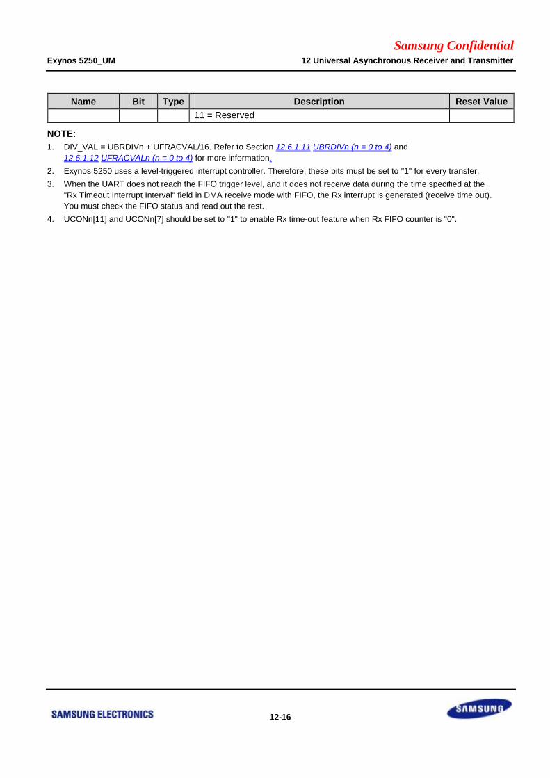
Samsung Confidential Exynos 5250_UM 12 Universal Asynchronous Receiver and Transmitter
12-16
Name Bit Type Description Reset Value
11 = Reserved
NOTE:
1. DIV_VAL = UBRDIVn + UFRACVAL/16. Refer to Section 12.6.1.11 UBRDIVn (n = 0 to 4) and
12.6.1.12 UFRACVALn (n = 0 to 4) for more information.
2. Exynos 5250 uses a level-triggered interrupt controller. Therefore, these bits must be set to "1" for every transfer.
3. When the UART does not reach the FIFO trigger level, and it does not receive data during the time specified at the
"Rx Timeout Interrupt Interval" field in DMA receive mode with FIFO, the Rx interrupt is generated (receive time out).
You must check the FIFO status and read out the rest.
4. UCONn[11] and UCONn[7] should be set to "1" to enable Rx time-out feature when Rx FIFO counter is "0".
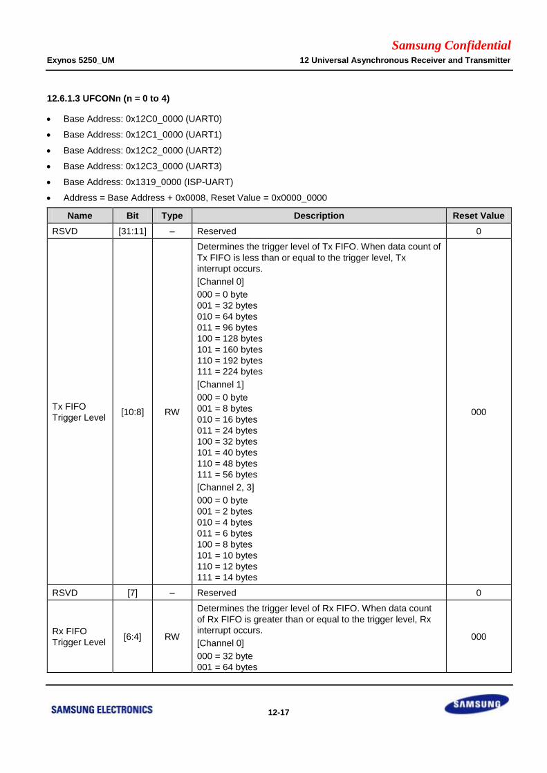
Samsung Confidential Exynos 5250_UM 12 Universal Asynchronous Receiver and Transmitter
12-17
12.6.1.3 UFCONn (n = 0 to 4)
Base Address: 0x12C0_0000 (UART0)
Base Address: 0x12C1_0000 (UART1)
Base Address: 0x12C2_0000 (UART2)
Base Address: 0x12C3_0000 (UART3)
Base Address: 0x1319_0000 (ISP-UART)
Address = Base Address + 0x0008, Reset Value = 0x0000_0000
Name Bit Type Description Reset Value
RSVD [31:11] – Reserved 0
Tx FIFO
Trigger Level [10:8] RW
Determines the trigger level of Tx FIFO. When data count of
Tx FIFO is less than or equal to the trigger level, Tx
interrupt occurs.
[Channel 0]
000 = 0 byte
001 = 32 bytes
010 = 64 bytes
011 = 96 bytes
100 = 128 bytes
101 = 160 bytes
110 = 192 bytes
111 = 224 bytes
[Channel 1]
000 = 0 byte
001 = 8 bytes
010 = 16 bytes
011 = 24 bytes
100 = 32 bytes
101 = 40 bytes
110 = 48 bytes
111 = 56 bytes
[Channel 2, 3]
000 = 0 byte
001 = 2 bytes
010 = 4 bytes
011 = 6 bytes
100 = 8 bytes
101 = 10 bytes
110 = 12 bytes
111 = 14 bytes
000
RSVD [7] – Reserved 0
Rx FIFO
Trigger Level [6:4] RW
Determines the trigger level of Rx FIFO. When data count
of Rx FIFO is greater than or equal to the trigger level, Rx
interrupt occurs.
[Channel 0]
000 = 32 byte
001 = 64 bytes
000
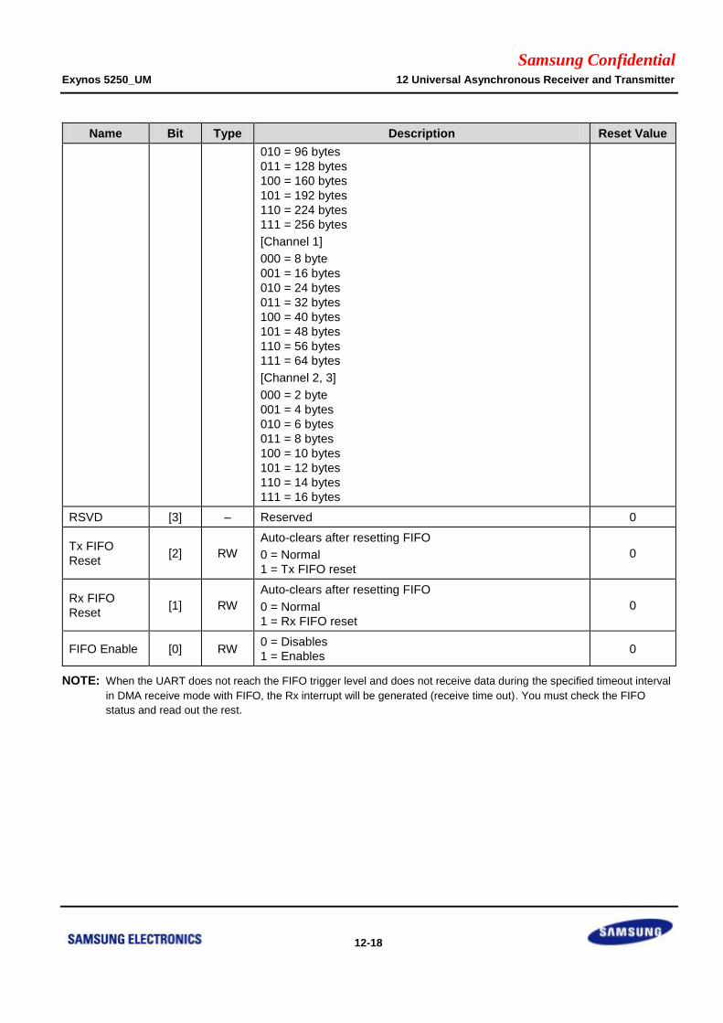
Samsung Confidential Exynos 5250_UM 12 Universal Asynchronous Receiver and Transmitter
12-18
Name Bit Type Description Reset Value
010 = 96 bytes
011 = 128 bytes
100 = 160 bytes
101 = 192 bytes
110 = 224 bytes
111 = 256 bytes
[Channel 1]
000 = 8 byte
001 = 16 bytes
010 = 24 bytes
011 = 32 bytes
100 = 40 bytes
101 = 48 bytes
110 = 56 bytes
111 = 64 bytes
[Channel 2, 3]
000 = 2 byte
001 = 4 bytes
010 = 6 bytes
011 = 8 bytes
100 = 10 bytes
101 = 12 bytes
110 = 14 bytes
111 = 16 bytes
RSVD [3] – Reserved 0
Tx FIFO
Reset [2] RW
Auto-clears after resetting FIFO
0 = Normal
1 = Tx FIFO reset
0
Rx FIFO
Reset [1] RW
Auto-clears after resetting FIFO
0 = Normal
1 = Rx FIFO reset
0
FIFO Enable [0] RW 0 = Disables
1 = Enables 0
NOTE: When the UART does not reach the FIFO trigger level and does not receive data during the specified timeout interval
in DMA receive mode with FIFO, the Rx interrupt will be generated (receive time out). You must check the FIFO
status and read out the rest.
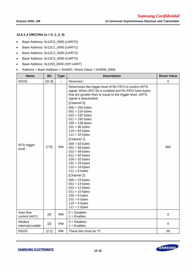
Samsung Confidential Exynos 5250_UM 12 Universal Asynchronous Receiver and Transmitter
12-19
12.6.1.4 UMCONn (n = 0, 1, 2, 4)
Base Address: 0x12C0_0000 (UART0)
Base Address: 0x12C1_0000 (UART1)
Base Address: 0x12C2_0000 (UART2)
Base Address: 0x12C3_0000 (UART3)
Base Address: 0x1319_0000 (ISP-UART)
Address = Base Address + 0x000C, Reset Value = 0x0000_0000
Name Bit Type Description Reset Value
RSVD [31:8] – Reserved 0
RTS trigger
level [7:5] RW
Determines the trigger level of Rx FIFO to control nRTS
signal. When AFC bit is enabled and Rx FIFO have bytes
that are greater than or equal to the trigger level, nRTS
signal is deactivated.
[Channel 0]
000 = 255 bytes
001 = 224 bytes
010 = 192 bytes
011 = 160 bytes
100 = 128 bytes
101 = 96 bytes
110 = 64 bytes
111 = 32 bytes
[Channel 1]
000 = 63 bytes
001 = 56 bytes
010 = 48 bytes
011 = 40 bytes
100 = 32 bytes
101 = 24 bytes
110 = 16 bytes
111 = 8 bytes
[Channel 2]
000 = 15 bytes
001 = 14 bytes
010 = 12 bytes
011 = 10 bytes
100 = 8 bytes
101 = 6 bytes
110 = 4 bytes
111 = 2 bytes
000
Auto flow
control (AFC) [4] RW
0 = Disables
1 = Enables 0
Modem
interrupt enable [3] RW
0 = Disables
1 = Enables 0
RSVD [2:1] RW These bits must be "0" 00

Samsung Confidential Exynos 5250_UM 12 Universal Asynchronous Receiver and Transmitter
12-20
Name Bit Type Description Reset Value
Request to
send [0] RW
When AFC bit is enabled, this value is ignored. In this case
the Exynos 5250 controls nRTS signals automatically.
When AFC bit is disabled, the software must control nRTS
signal.
0 = "H" level (Inactivate nRTS)
1 = "L" level (Activate nRTS)
0
NOTE:
1. UART 2 supports AFC function, when XuRTSn_2 and XuCTSn_2 are set as nRTS2 and nCTS2 by GPA1CON.
UART 3 does not support AFC function, because the Exynos 5250 does not contain nRTS3 and nCTS3.
2. In AFC mode, Rx FIFO trigger level should be set to lower than RTS trigger level, because transmitter stops data
transfer when it gets deactivated nRST signal.
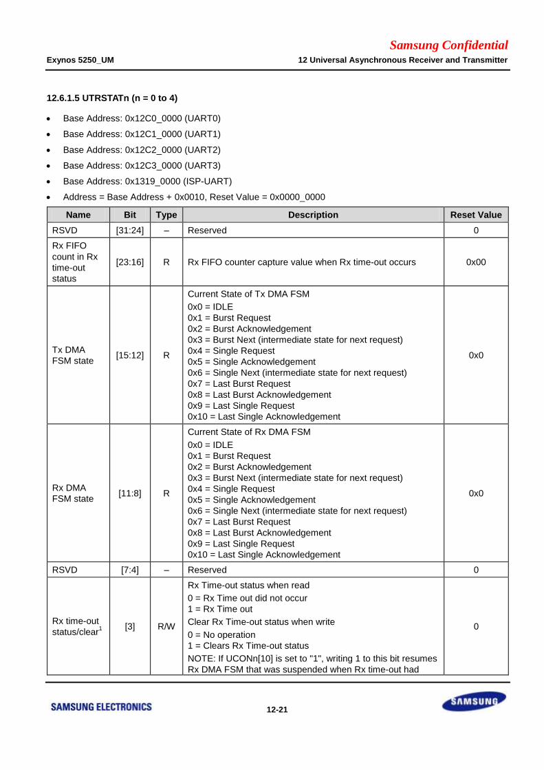
Samsung Confidential Exynos 5250_UM 12 Universal Asynchronous Receiver and Transmitter
12-21
12.6.1.5 UTRSTATn (n = 0 to 4)
Base Address: 0x12C0_0000 (UART0)
Base Address: 0x12C1_0000 (UART1)
Base Address: 0x12C2_0000 (UART2)
Base Address: 0x12C3_0000 (UART3)
Base Address: 0x1319_0000 (ISP-UART)
Address = Base Address + 0x0010, Reset Value = 0x0000_0000
Name Bit Type Description Reset Value
RSVD [31:24] – Reserved 0
Rx FIFO
count in Rx
time-out
status
[23:16] R Rx FIFO counter capture value when Rx time-out occurs 0x00
Tx DMA
FSM state [15:12] R
Current State of Tx DMA FSM
0x0 = IDLE
0x1 = Burst Request
0x2 = Burst Acknowledgement
0x3 = Burst Next (intermediate state for next request)
0x4 = Single Request
0x5 = Single Acknowledgement
0x6 = Single Next (intermediate state for next request)
0x7 = Last Burst Request
0x8 = Last Burst Acknowledgement
0x9 = Last Single Request
0x10 = Last Single Acknowledgement
0x0
Rx DMA
FSM state [11:8] R
Current State of Rx DMA FSM
0x0 = IDLE
0x1 = Burst Request
0x2 = Burst Acknowledgement
0x3 = Burst Next (intermediate state for next request)
0x4 = Single Request
0x5 = Single Acknowledgement
0x6 = Single Next (intermediate state for next request)
0x7 = Last Burst Request
0x8 = Last Burst Acknowledgement
0x9 = Last Single Request
0x10 = Last Single Acknowledgement
0x0
RSVD [7:4] – Reserved 0
Rx time-out
status/clear1
[3] R/W
Rx Time-out status when read
0 = Rx Time out did not occur
1 = Rx Time out
Clear Rx Time-out status when write
0 = No operation
1 = Clears Rx Time-out status
NOTE: If UCONn[10] is set to "1", writing 1 to this bit resumes
Rx DMA FSM that was suspended when Rx time-out had
0
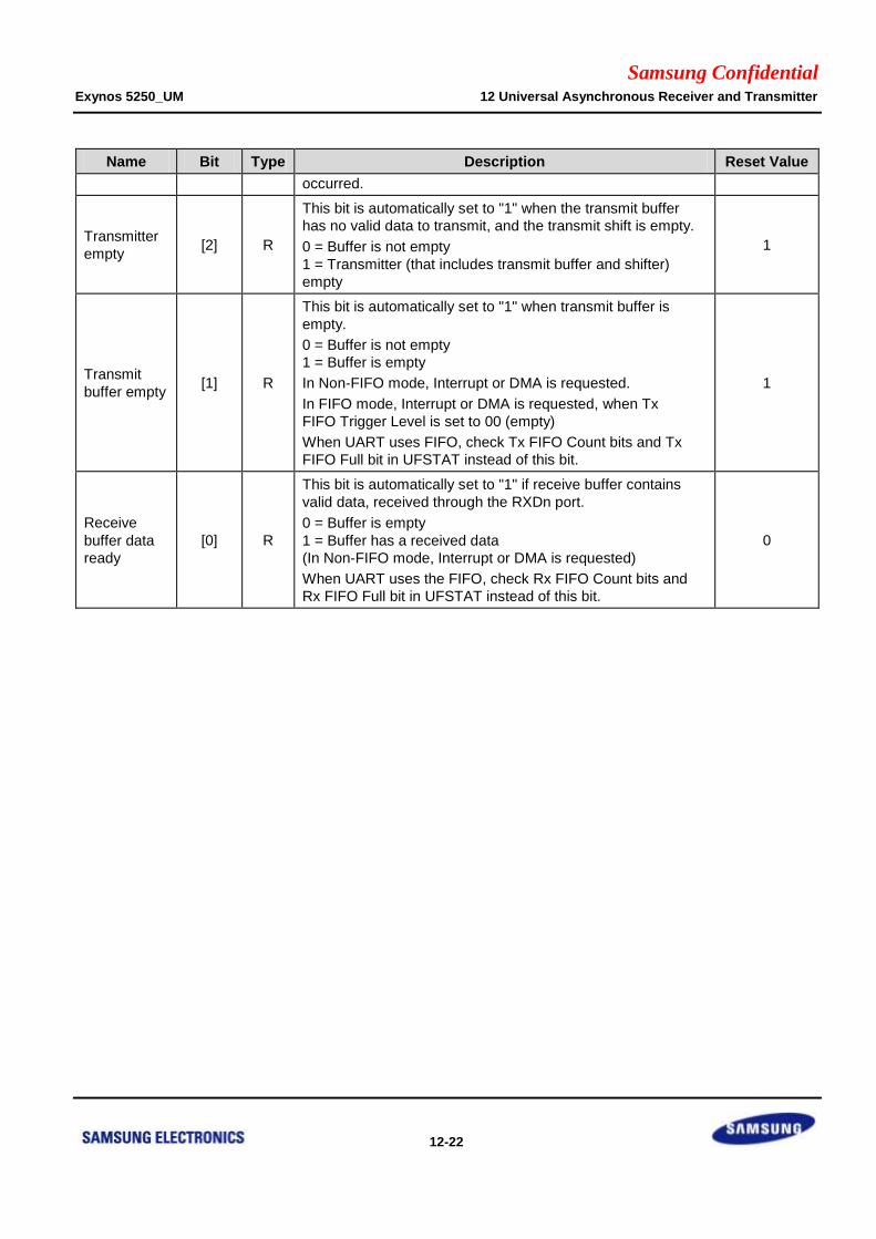
Samsung Confidential Exynos 5250_UM 12 Universal Asynchronous Receiver and Transmitter
12-22
Name Bit Type Description Reset Value
occurred.
Transmitter
empty [2] R
This bit is automatically set to "1" when the transmit buffer
has no valid data to transmit, and the transmit shift is empty.
0 = Buffer is not empty
1 = Transmitter (that includes transmit buffer and shifter)
empty
1
Transmit
buffer empty [1] R
This bit is automatically set to "1" when transmit buffer is
empty.
0 = Buffer is not empty
1 = Buffer is empty
In Non-FIFO mode, Interrupt or DMA is requested.
In FIFO mode, Interrupt or DMA is requested, when Tx
FIFO Trigger Level is set to 00 (empty)
When UART uses FIFO, check Tx FIFO Count bits and Tx
FIFO Full bit in UFSTAT instead of this bit.
1
Receive
buffer data
ready
[0] R
This bit is automatically set to "1" if receive buffer contains
valid data, received through the RXDn port.
0 = Buffer is empty
1 = Buffer has a received data
(In Non-FIFO mode, Interrupt or DMA is requested)
When UART uses the FIFO, check Rx FIFO Count bits and
Rx FIFO Full bit in UFSTAT instead of this bit.
0
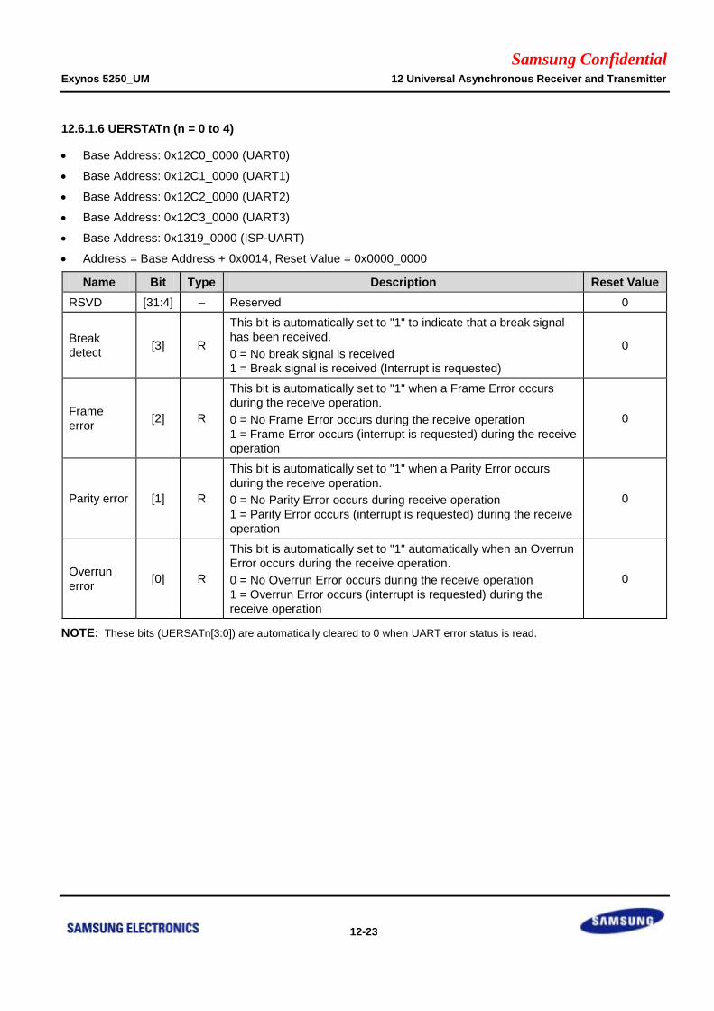
Samsung Confidential Exynos 5250_UM 12 Universal Asynchronous Receiver and Transmitter
12-23
12.6.1.6 UERSTATn (n = 0 to 4)
Base Address: 0x12C0_0000 (UART0)
Base Address: 0x12C1_0000 (UART1)
Base Address: 0x12C2_0000 (UART2)
Base Address: 0x12C3_0000 (UART3)
Base Address: 0x1319_0000 (ISP-UART)
Address = Base Address + 0x0014, Reset Value = 0x0000_0000
Name Bit Type Description Reset Value
RSVD [31:4] – Reserved 0
Break
detect [3] R
This bit is automatically set to "1" to indicate that a break signal
has been received.
0 = No break signal is received
1 = Break signal is received (Interrupt is requested)
0
Frame
error [2] R
This bit is automatically set to "1" when a Frame Error occurs
during the receive operation.
0 = No Frame Error occurs during the receive operation
1 = Frame Error occurs (interrupt is requested) during the receive
operation
0
Parity error [1] R
This bit is automatically set to "1" when a Parity Error occurs
during the receive operation.
0 = No Parity Error occurs during receive operation
1 = Parity Error occurs (interrupt is requested) during the receive
operation
0
Overrun
error [0] R
This bit is automatically set to "1" automatically when an Overrun
Error occurs during the receive operation.
0 = No Overrun Error occurs during the receive operation
1 = Overrun Error occurs (interrupt is requested) during the
receive operation
0
NOTE: These bits (UERSATn[3:0]) are automatically cleared to 0 when UART error status is read.
Samsung Confidential Exynos 5250_UM 12 Universal Asynchronous Receiver and Transmitter
12-24
12.6.1.7 UFSTATn (n = 0 to 4)
Base Address: 0x12C0_0000 (UART0)
Base Address: 0x12C1_0000 (UART1)
Base Address: 0x12C2_0000 (UART2)
Base Address: 0x12C3_0000 (UART3)
Base Address: 0x1319_0000 (ISP-UART)
Address = Base Address + 0x0018, Reset Value = 0x0000_0000
Name Bit Type Description Reset Value
RSVD [31:25] – Reserved 0
Tx FIFO full [24] R
This bit is automatically set to "1" when the transmitted FIFO
is full during transmit operation.
0 = Not Full
1 = Full
0
Tx FIFO
count [23:16] R
Number of data in Tx FIFO
NOTE: This field is set to "0" when Tx FIFO is full. 0
RSVD [15:10] – Reserved 0
Rx FIFO
error [9] R
This bit is set to "1" when Rx FIFO contains invalid data
which results due to Frame Error, Parity Error, or Break
Signal.
0
Rx FIFO full [8] R
This bit is automatically set to "1" when the received FIFO is
full during receive operation.
0 = Not Full
1 = Full
0
Rx FIFO
count [7:0] R
Number of data in Rx FIFO
NOTE: This field is set to "0" when Rx FIFO is full. 0
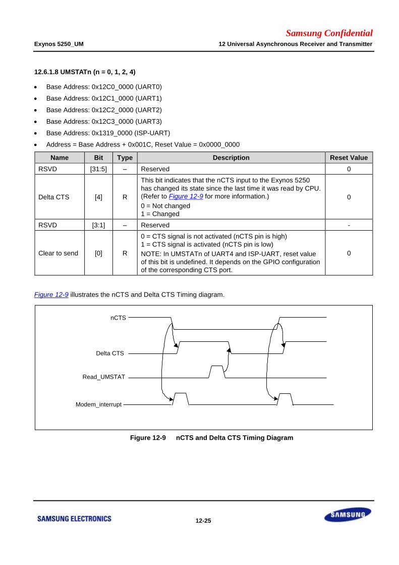
Samsung Confidential Exynos 5250_UM 12 Universal Asynchronous Receiver and Transmitter
12-25
12.6.1.8 UMSTATn (n = 0, 1, 2, 4)
Base Address: 0x12C0_0000 (UART0)
Base Address: 0x12C1_0000 (UART1)
Base Address: 0x12C2_0000 (UART2)
Base Address: 0x12C3_0000 (UART3)
Base Address: 0x1319_0000 (ISP-UART)
Address = Base Address + 0x001C, Reset Value = 0x0000_0000
Name Bit Type Description Reset Value
RSVD [31:5] – Reserved 0
Delta CTS [4] R
This bit indicates that the nCTS input to the Exynos 5250
has changed its state since the last time it was read by CPU.
(Refer to Figure 12-9 for more information.)
0 = Not changed
1 = Changed
0
RSVD [3:1] – Reserved -
Clear to send [0] R
0 = CTS signal is not activated (nCTS pin is high)
1 = CTS signal is activated (nCTS pin is low)
NOTE: In UMSTATn of UART4 and ISP-UART, reset value
of this bit is undefined. It depends on the GPIO configuration
of the corresponding CTS port.
0
Figure 12-9 illustrates the nCTS and Delta CTS Timing diagram.
Figure 12-9 nCTS and Delta CTS Timing Diagram
nCTS
Delta CTS
Read_UMSTAT
Modem_interrupt
Samsung Confidential Exynos 5250_UM 12 Universal Asynchronous Receiver and Transmitter
12-26
12.6.1.9 UTXHn (n = 0 to 4)
Base Address: 0x12C0_0000 (UART0)
Base Address: 0x12C1_0000 (UART1)
Base Address: 0x12C2_0000 (UART2)
Base Address: 0x12C3_0000 (UART3)
Base Address: 0x1319_0000 (ISP-UART)
Address = Base Address + 0x0020, Reset Value = 0x0000_0000
Name Bit Type Description Reset Value
RSVD [31:8] – Reserved –
UTXHn [7:0] W Transmit Data for UARTn –
12.6.1.10 URXHn (n = 0 to 4)
Base Address: 0x12C0_0000 (UART0)
Base Address: 0x12C1_0000 (UART1)
Base Address: 0x12C2_0000 (UART2)
Base Address: 0x12C3_0000 (UART3)
Base Address: 0x1319_0000 (ISP-UART)
Address = Base Address + 0x0024, Reset Value = 0x0000_0000
Name Bit Type Description Reset Value
RSVD [31:8] – Reserved 0
URXHn [7:0] R Receive Data for UARTn 0x00
NOTE: When an Overrun Error occurs, the URXHn must be read. If not, the next received data makes an Overrun Error,
even though the overrun bit of UERSTATn had been cleared.
12.6.1.11 UBRDIVn (n = 0 to 4)
Base Address: 0x12C0_0000 (UART0)
Base Address: 0x12C1_0000 (UART1)
Base Address: 0x12C2_0000 (UART2)
Base Address: 0x12C3_0000 (UART3)
Base Address: 0x1319_0000 (ISP-UART)
Address = Base Address + 0x0028, Reset Value = 0x0000_0000
Name Bit Type Description Reset Value
RSVD [31:16] – Reserved 0
UBRDIVn [15:0] RW Baud Rate Division Value
NOTE: UBRDIV value must be greater than 0. 0x0000

Samsung Confidential Exynos 5250_UM 12 Universal Asynchronous Receiver and Transmitter
12-27
12.6.1.12 UFRACVALn (n = 0 to 4)
Base Address: 0x12C0_0000 (UART0)
Base Address: 0x12C1_0000 (UART1)
Base Address: 0x12C2_0000 (UART2)
Base Address: 0x12C3_0000 (UART3)
Base Address: 0x1319_0000 (ISP-UART)
Address = Base Address + 0x002C, Reset Value = 0x0000_0000
Name Bit Type Description Reset Value
RSVD [31:4] – Reserved 0
UFRACVALn [3:0] RW Determines the fractional part of Baud Rate Divisor 0x0
1. UART Baud Rate Configuration
The value stored in the Baud Rate Divisor (UBRDIVn) and Divisor Fractional value (UFRACVALn) is
used to determine the serial Tx/Rx clock rate (baud rate) as:
DIV_VAL = UBRDIVn + UFRACVALn/16
Or
DIV_VAL = (SCLK_UART/(bps 16)) – 1
Where, the divisor should be from 1 to (216 – 1).
Using UFRACVALn, you can generate the Baud Rate more accurately.
For example, when the Baud Rate is 115200 bps and SCLK_UART is 40 MHz, UBRDIVn and UFRACVALn are:
DIV_VAL = (40000000/(115200 16)) – 1
= 21.7 – 1
= 20.7
UBRDIVn = 20 (integer part of DIV_VAL)
UFRACVALn/16 = 0.7
so, UFRACVALn = 11
2. Baud Rate Error Tolerance
UART Frame error should be less than 1.87 % (3/160)
tUPCLK = (UBRDIVn + 1 + UFRACVAL/16) 16 1Frame/SCLK_UART
tUPCLK: Real UART Clock
tEXTUARTCLK = 1Frame/baud-rate
tEXTUARTCLK: Ideal UART Clock
UART error = (tUPCLK – tEXTUARTCLK)/tEXTUARTCLK 100 %
* 1Frame = start bit + data bit + parity bit + stop bit.
3. UART Clock and PCLK Relation
There is a constraint on the ratio of clock frequencies for PCLK to UARTCLK.
The frequency of UARTCLK must not be more than 5.5/3 times faster than the frequency of PCLK:
FUARTCLK 5.5/3 FPCLK
Samsung Confidential Exynos 5250_UM 12 Universal Asynchronous Receiver and Transmitter
12-28
FUARTCLK = baudrate 16
This allows sufficient time to write the received data to the receive FIFO.
Samsung Confidential Exynos 5250_UM 12 Universal Asynchronous Receiver and Transmitter
12-29
12.6.1.13 UINTPn (n = 0 to 4)
Base Address: 0x12C0_0000 (UART0)
Base Address: 0x12C1_0000 (UART1)
Base Address: 0x12C2_0000 (UART2)
Base Address: 0x12C3_0000 (UART3)
Base Address: 0x1319_0000 (ISP-UART)
Address = Base Address + 0x0030, Reset Value = 0x0000_0000
Name Bit Type Description Reset Value
RSVD [31:4] – Reserved 0
MODEM [3] RW Generates Modem interrupt 0
TXD [2] RW Generates Transmit interrupt 0
ERROR [1] RW Generates Error interrupt 0
RXD [0] RW Generates Receive interrupt 0
Interrupt pending contains information of the interrupts that are generated.
If one of these 4 bits is logical high ("1"), each UART channel generates interrupt.
This must be cleared in the interrupt service routine after clearing interrupt pending in Interrupt Controller (INTC).
Clear specific bits of UINTP by writing "1" to the bits that you want to clear.
12.6.1.14 UINTSn (n = 0 to 4)
Base Address: 0x12C0_0000 (UART0)
Base Address: 0x12C1_0000 (UART1)
Base Address: 0x12C2_0000 (UART2)
Base Address: 0x12C3_0000 (UART3)
Base Address: 0x1319_0000 (ISP-UART)
Address = Base Address + 0x0034, Reset Value = 0x0000_0000
Name Bit Type Description Reset Value
RSVD [31:4] – Reserved 0
MODEM [3] R Generates Modem interrupt 0
TXD [2] R Generates Transmit interrupt 0
ERROR [1] R Generates Error interrupt 0
RXD [0] R Generates Receive interrupt 0
Interrupt Source contains information of the interrupt that are generated, regardless of the value of Interrupt Mask.
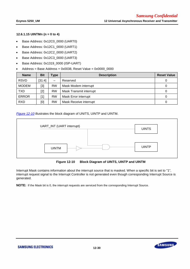
Samsung Confidential Exynos 5250_UM 12 Universal Asynchronous Receiver and Transmitter
12-30
12.6.1.15 UINTMn (n = 0 to 4)
Base Address: 0x12C0_0000 (UART0)
Base Address: 0x12C1_0000 (UART1)
Base Address: 0x12C2_0000 (UART2)
Base Address: 0x12C3_0000 (UART3)
Base Address: 0x1319_0000 (ISP-UART)
Address = Base Address + 0x0038, Reset Value = 0x0000_0000
Name Bit Type Description Reset Value
RSVD [31:4] – Reserved 0
MODEM [3] RW Mask Modem interrupt 0
TXD [2] RW Mask Transmit interrupt 0
ERROR [1] RW Mask Error interrupt 0
RXD [0] RW Mask Receive interrupt 0
Figure 12-10 illustrates the block diagram of UNITS, UINTP and UINTM.
UART_INT (UART interrupt)UINTS
UINTPUINTM
Figure 12-10 Block Diagram of UINTS, UINTP and UINTM
Interrupt Mask contains information about the interrupt source that is masked. When a specific bit is set to "1",
interrupt request signal to the Interrupt Controller is not generated even though corresponding Interrupt Source is
generated.
NOTE: If the Mask bit is 0, the interrupt requests are serviced from the corresponding Interrupt Source.
Samsung Confidential Exynos 5250_UM 13 IIC-Bus Interface
13-1
13 IIC-Bus Interface
13.1 Overview
The Exynos 5250 RISC microprocessor supports four multi-master I2C-bus serial interfaces. To transmit
information between bus masters and peripheral devices connected to the I2C-bus, a dedicated Serial Data Line
(SDA) and a Serial Clock Line (SCL) is used. Both SDA and SCL lines are bi-directional.
In multi-master I2C-bus mode, multiple Exynos 5250 RISC microprocessors receive or transmit serial data to or
from slave devices. The master Exynos 5250 initiates and terminates a data transfer through the I2C-bus. The I
2C-
bus in the Exynos 5250 uses a standard bus arbitration procedure.
To control multi-master I2C-bus operations, values must be written to the following registers:
Multi-master I2C-bus control register-I2CCON
Multi-master I2C-bus control/status register-I2CSTAT
Multi-master I2C-bus Tx/Rx data shift register-I2CDS
Multi-master I2C-bus address register-I2CADD
When the I2C-bus is free, both SDA and SCL lines should be at High level. A High-to-Low transition of SDA
initiates a Start condition. A Low-to-High transition of SDA initiates a Stop condition, while SCL remains steady at
High Level.
The master device always generates Start and Stop conditions. First 7-bit address value in the data byte that is
transferred through SDA line after the Start condition has been initiated, can determine the slave device, which the
bus master device has selected. The 8th bit determines the direction of the transfer (Read or Write).
Every data byte that is transmitted to the SDA line should be eight bits in total. There is no limit to send or receive
bytes during the Bus Transfer operation. Data is always sent from Most-Significant Bit (MSB) first, and every byte
should be immediately followed by an acknowledgement (ACK) bit.
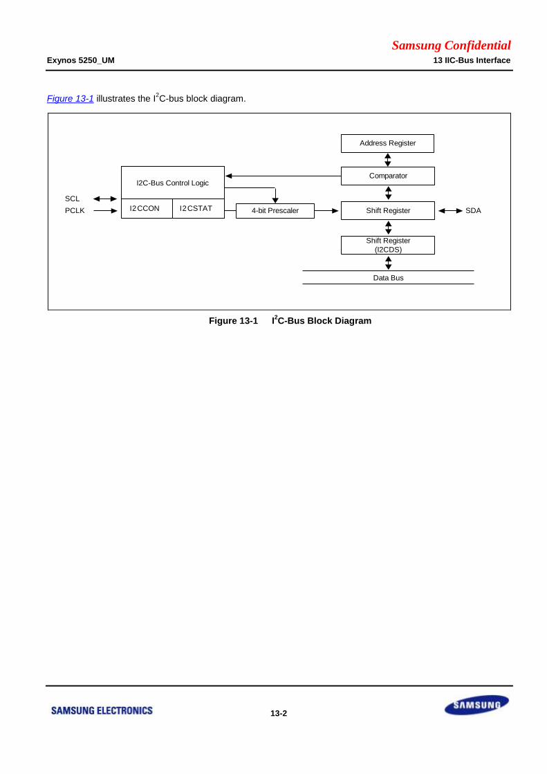
Samsung Confidential Exynos 5250_UM 13 IIC-Bus Interface
13-2
Figure 13-1 illustrates the I2C-bus block diagram.
Figure 13-1 I2C-Bus Block Diagram
PCLK
Address Register
SDA4-bit Prescaler
I2C-Bus Control Logic
I2CSTATI2CCON
Comparator
Shift Register
Shift Register
(I2CDS)
Data Bus
SCL
Samsung Confidential Exynos 5250_UM 13 IIC-Bus Interface
13-3
13.2 Features
9-channels Multi-Master, Slave I2C-bus interfaces
(8-channels for general purpose, 1-channel for HDMI dedicated)
7-bit addressing mode
Serial, 8-bit oriented, and bi-directional data transfer
Supports up to 100 kbit/s in the Standard Mode
Supports up to 400 kbit/s in the Fast Mode
Supports Master Transmit, Master Receive, Slave Transmit and Slave Receive operation
Supports Interrupt or Polling events
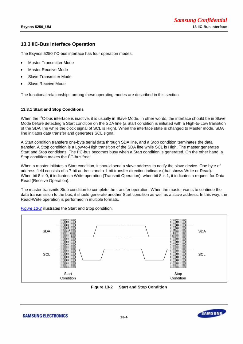
Samsung Confidential Exynos 5250_UM 13 IIC-Bus Interface
13-4
13.3 IIC-Bus Interface Operation
The Exynos 5250 I2C-bus interface has four operation modes:
Master Transmitter Mode
Master Receive Mode
Slave Transmitter Mode
Slave Receive Mode
The functional relationships among these operating modes are described in this section.
13.3.1 Start and Stop Conditions
When the I2C-bus interface is inactive, it is usually in Slave Mode. In other words, the interface should be in Slave
Mode before detecting a Start condition on the SDA line (a Start condition is initiated with a High-to-Low transition
of the SDA line while the clock signal of SCL is High). When the interface state is changed to Master mode, SDA
line initiates data transfer and generates SCL signal.
A Start condition transfers one-byte serial data through SDA line, and a Stop condition terminates the data
transfer. A Stop condition is a Low-to-High transition of the SDA line while SCL is High. The master generates
Start and Stop conditions. The I2C-bus becomes busy when a Start condition is generated. On the other hand, a
Stop condition makes the I2C-bus free.
When a master initiates a Start condition, it should send a slave address to notify the slave device. One byte of
address field consists of a 7-bit address and a 1-bit transfer direction indicator (that shows Write or Read).
When bit 8 is 0, it indicates a Write operation (Transmit Operation); when bit 8 is 1, it indicates a request for Data
Read (Receive Operation).
The master transmits Stop condition to complete the transfer operation. When the master wants to continue the
data transmission to the bus, it should generate another Start condition as well as a slave address. In this way, the
Read-Write operation is performed in multiple formats.
Figure 13-2 illustrates the Start and Stop condition.
Figure 13-2 Start and Stop Condition
SCL
SDA SDA
SCL
Start
Condition
Stop
Condition
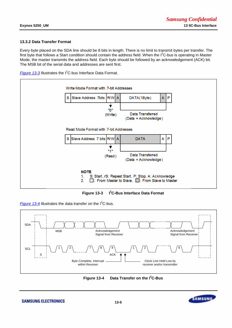
Samsung Confidential Exynos 5250_UM 13 IIC-Bus Interface
13-5
13.3.2 Data Transfer Format
Every byte placed on the SDA line should be 8 bits in length. There is no limit to transmit bytes per transfer. The
first byte that follows a Start condition should contain the address field. When the I2C-bus is operating in Master
Mode, the master transmits the address field. Each byte should be followed by an acknowledgement (ACK) bit.
The MSB bit of the serial data and addresses are sent first.
Figure 13-3 illustrates the I2C-bus Interface Data Format.
Figure 13-3 I2C-Bus Interface Data Format
Figure 13-4 illustrates the data transfer on the I2C-bus.
Figure 13-4 Data Transfer on the I2C-Bus
SDA
Acknowledgement
Signal from Receiver
SCL
S
1 2 7 8 9 1 2 9
Acknowledgement
Signal from ReceiverMSB
ACK
Byte Complete, Interrupt
within Receiver
Clock Line Held Low by
receiver and/or transmitter
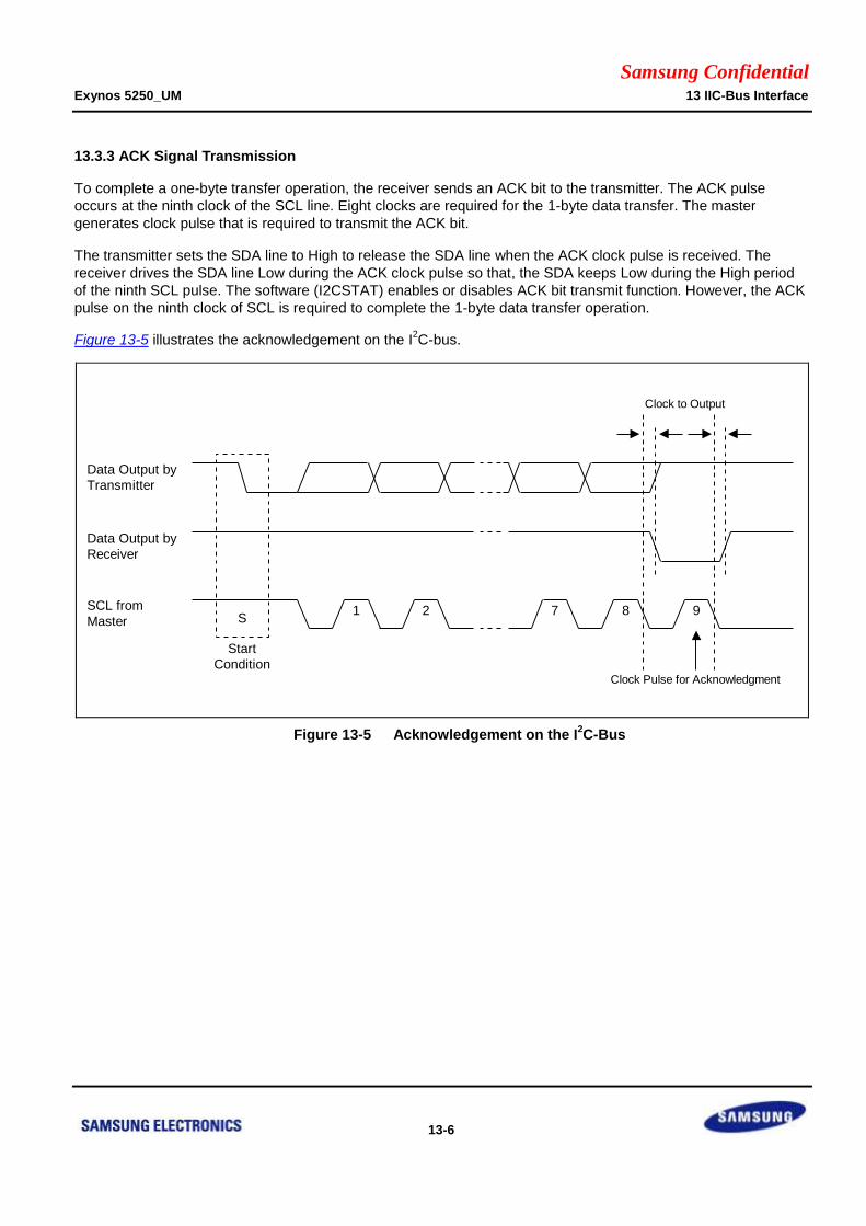
Samsung Confidential Exynos 5250_UM 13 IIC-Bus Interface
13-6
13.3.3 ACK Signal Transmission
To complete a one-byte transfer operation, the receiver sends an ACK bit to the transmitter. The ACK pulse
occurs at the ninth clock of the SCL line. Eight clocks are required for the 1-byte data transfer. The master
generates clock pulse that is required to transmit the ACK bit.
The transmitter sets the SDA line to High to release the SDA line when the ACK clock pulse is received. The
receiver drives the SDA line Low during the ACK clock pulse so that, the SDA keeps Low during the High period
of the ninth SCL pulse. The software (I2CSTAT) enables or disables ACK bit transmit function. However, the ACK
pulse on the ninth clock of SCL is required to complete the 1-byte data transfer operation.
Figure 13-5 illustrates the acknowledgement on the I2C-bus.
Figure 13-5 Acknowledgement on the I2C-Bus
Data Output by
Transmitter
Data Output by
Receiver
SCL from
Master
Start
ConditionClock Pulse for Acknowledgment
Clock to Output
987S
1 2
Samsung Confidential Exynos 5250_UM 13 IIC-Bus Interface
13-7
13.3.4 Read-Write Operation
When data is transmitted in Transmitter Mode, the I2C-bus interface waits until I
2C-bus Data Shift (I2CDS) register
receives the new data. Before the new data is written to the register, the SCL line is held Low. The line is released
only after the data has been written. Exynos 5250 holds the interrupt to identify the completion of current data
transfer. After the CPU receives the interrupt request, it writes new data to the I2CDS register again.
When data is received in Receive Mode, the I2C-bus interface waits until I2CDS register is read. Before the new
data is read out, the SCL line is held Low. The line is released only after the data has been read. Exynos 5250
holds the interrupt to identify the completion of new data reception. After the CPU receives the interrupt request, it
reads the data from the I2CDS register.
13.3.5 Bus Arbitration Procedures
Arbitration occurs on the SDA line to prevent the contention on the bus between two masters. When a master with
a SDA High level, detects other master with a SDA active Low level, it does not initiate a data transfer because
the current level on the bus, does not correspond to its own. The arbitration procedure extends until the SDA line
turns High.
When the masters lower the SDA line, simultaneously each master evaluates whether the mastership is allocated
by itself or not. For the purpose of evaluation, each master detects the address bits. While each master generates
the slave address, it detects the address bit on the SDA line because the SDA line is likely to become Low than
High.
In a situation where one master generates a Low as first address bit, while the other master is maintaining High. In
this case, both masters detect Low on the bus, because the Low status is superior to the High status in power.
When this happens, Low (as the first bit of address) generating master gets the mastership while High (as the first
bit of address) generating master withdraws the mastership. When both masters generate Low as the first bit of
address, there is arbitration for the second address bit again. This arbitration continues till the end of last address
bit.
13.3.6 Abort Conditions
When a slave receiver cannot acknowledge the confirmation of the slave address, it holds the level of the SDA
line as High. In this case, the master generates a Stop condition and cancels the transfer.
When a master receiver is involved in the aborted transfer, it signals the end of slave transmit operation by
canceling the generation of an ACK. It performs this after the last data byte was received from the slave. The
slave transmitter releases the SDA to allow a master to generate a Stop condition.
13.3.7 Configuring IIC-Bus
To control the frequency of the Serial Clock (SCL), the 4-bit prescaler value is programmed in the I2CCON
register. The I2C-bus interface address is stored in the I
2C-bus address (I2CADD) register (by default, the I
2C-bus
interface address has an unknown value).
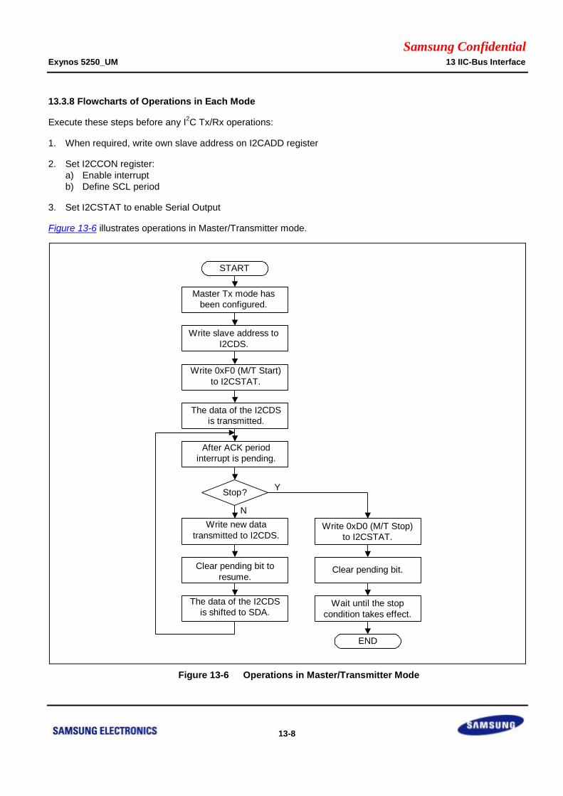
Samsung Confidential Exynos 5250_UM 13 IIC-Bus Interface
13-8
13.3.8 Flowcharts of Operations in Each Mode
Execute these steps before any I2C Tx/Rx operations:
1. When required, write own slave address on I2CADD register
2. Set I2CCON register:
a) Enable interrupt
b) Define SCL period
3. Set I2CSTAT to enable Serial Output
Figure 13-6 illustrates operations in Master/Transmitter mode.
Figure 13-6 Operations in Master/Transmitter Mode
Write slave address to
I2CDS.
Write 0xF0 (M/T Start)
to I2CSTAT.
The data of the I2CDS
is transmitted.
After ACK period
interrupt is pending.
Write 0xD0 (M/T Stop)
to I2CSTAT.
Write new data
transmitted to I2CDS.
Stop?
Clear pending bit to
resume.
The data of the I2CDS
is shifted to SDA.
START
Master Tx mode has
been configured.
Clear pending bit.
Wait until the stop
condition takes effect.
END
Y
N
Samsung Confidential Exynos 5250_UM 13 IIC-Bus Interface
13-9
NOTE: When Master transmit mode, stop sequence of I2C_HDMI and I2C_SATAPHY is as follows
Write 0xD0 to I2CSTAT clear pending bit Wait until the stop condition take effect
Write 0xC0 to I2CSTAT END
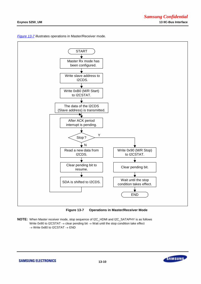
Samsung Confidential Exynos 5250_UM 13 IIC-Bus Interface
13-10
Figure 13-7 illustrates operations in Master/Receiver mode.
Figure 13-7 Operations in Master/Receiver Mode
NOTE: When Master receiver mode, stop sequence of I2C_HDMI and I2C_SATAPHY is as follows
Write 0x90 to I2CSTAT clear pending bit Wait until the stop condition take effect
Write 0x80 to I2CSTAT END
Write slave address to
I2CDS.
Write 0xB0 (M/R Start)
to I2CSTAT.
The data of the I2CDS
(Slave address) is transmitted.
After ACK period
interrupt is pending.
Write 0x90 (M/R Stop)
to I2CSTAT.
Read a new data from
I2CDS.
Stop ?
Clear pending bit to
resume.
SDA is shifted to I2CDS.
START
Master Rx mode has
been configured.
Clear pending bit.
Wait until the stop
condition takes effect.
END
Y
N

Samsung Confidential Exynos 5250_UM 13 IIC-Bus Interface
13-11
Figure 13-8 illustrates operations in Slave/Transmitter mode.
Figure 13-8 Operations in Slave/Transmitter Mode
I2C detects start signal. and, I2CDS
receives data.
I2C compares I2CADD and I2CDS
(the received slave address).
Write data to I2CDS.
Clear pending bit to
resume.
The data of the I2CDS
is shifted to SDA.
START
Slave Tx mode has
been configured.
END
Matched ?
N
Y
Stop ?
Interrupt is pending.
N
Y
The I2C address match
interrupt is generated.
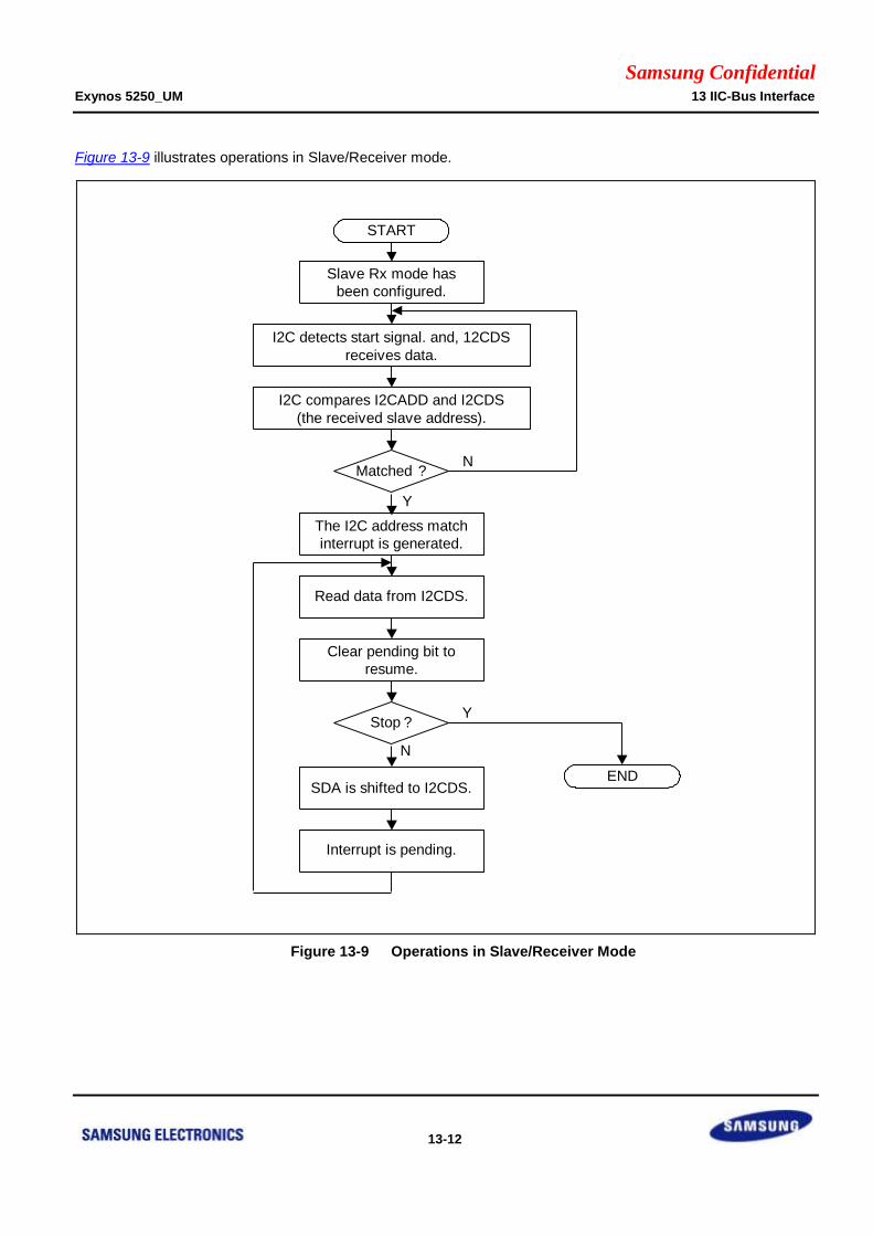
Samsung Confidential Exynos 5250_UM 13 IIC-Bus Interface
13-12
Figure 13-9 illustrates operations in Slave/Receiver mode.
Figure 13-9 Operations in Slave/Receiver Mode
I2C detects start signal. and, 12CDS
receives data.
I2C compares I2CADD and I2CDS
(the received slave address).
Read data from I2CDS.
Clear pending bit to
resume.
SDA is shifted to I2CDS.
START
Slave Rx mode has
been configured.
END
Matched ?
N
Y
Stop ?
Interrupt is pending.
N
Y
The I2C address match
interrupt is generated.
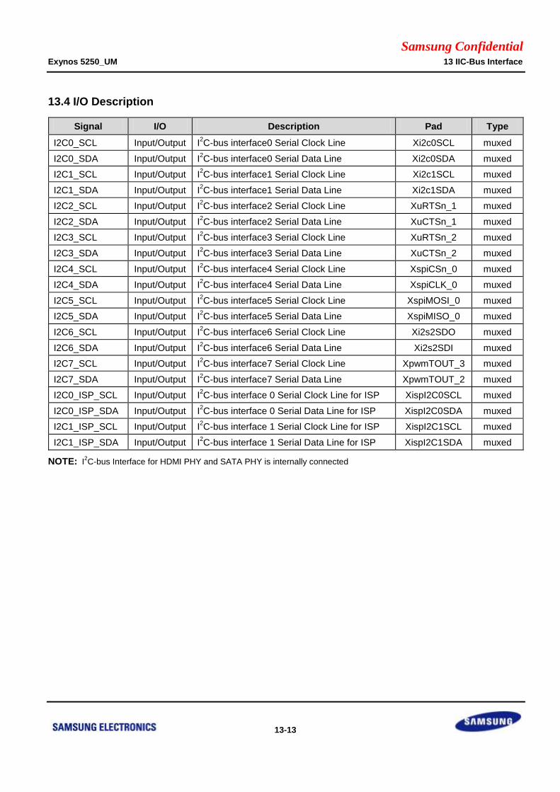
Samsung Confidential Exynos 5250_UM 13 IIC-Bus Interface
13-13
13.4 I/O Description
Signal I/O Description Pad Type
I2C0_SCL Input/Output I2C-bus interface0 Serial Clock Line Xi2c0SCL muxed
I2C0_SDA Input/Output I2C-bus interface0 Serial Data Line Xi2c0SDA muxed
I2C1_SCL Input/Output I2C-bus interface1 Serial Clock Line Xi2c1SCL muxed
I2C1_SDA Input/Output I2C-bus interface1 Serial Data Line Xi2c1SDA muxed
I2C2_SCL Input/Output I2C-bus interface2 Serial Clock Line XuRTSn_1 muxed
I2C2_SDA Input/Output I2C-bus interface2 Serial Data Line XuCTSn_1 muxed
I2C3_SCL Input/Output I2C-bus interface3 Serial Clock Line XuRTSn_2 muxed
I2C3_SDA Input/Output I2C-bus interface3 Serial Data Line XuCTSn_2 muxed
I2C4_SCL Input/Output I2C-bus interface4 Serial Clock Line XspiCSn_0 muxed
I2C4_SDA Input/Output I2C-bus interface4 Serial Data Line XspiCLK_0 muxed
I2C5_SCL Input/Output I2C-bus interface5 Serial Clock Line XspiMOSI_0 muxed
I2C5_SDA Input/Output I2C-bus interface5 Serial Data Line XspiMISO_0 muxed
I2C6_SCL Input/Output I2C-bus interface6 Serial Clock Line Xi2s2SDO muxed
I2C6_SDA Input/Output I2C-bus interface6 Serial Data Line Xi2s2SDI muxed
I2C7_SCL Input/Output I2C-bus interface7 Serial Clock Line XpwmTOUT_3 muxed
I2C7_SDA Input/Output I2C-bus interface7 Serial Data Line XpwmTOUT_2 muxed
I2C0_ISP_SCL Input/Output I2C-bus interface 0 Serial Clock Line for ISP XispI2C0SCL muxed
I2C0_ISP_SDA Input/Output I2C-bus interface 0 Serial Data Line for ISP XispI2C0SDA muxed
I2C1_ISP_SCL Input/Output I2C-bus interface 1 Serial Clock Line for ISP XispI2C1SCL muxed
I2C1_ISP_SDA Input/Output I2C-bus interface 1 Serial Data Line for ISP XispI2C1SDA muxed
NOTE: I2C-bus Interface for HDMI PHY and SATA PHY is internally connected
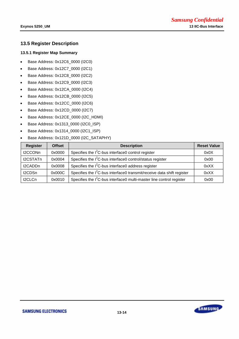
Samsung Confidential Exynos 5250_UM 13 IIC-Bus Interface
13-14
13.5 Register Description
13.5.1 Register Map Summary
Base Address: 0x12C6_0000 (I2C0)
Base Address: 0x12C7_0000 (I2C1)
Base Address: 0x12C8_0000 (I2C2)
Base Address: 0x12C9_0000 (I2C3)
Base Address: 0x12CA_0000 (I2C4)
Base Address: 0x12CB_0000 (I2C5)
Base Address: 0x12CC_0000 (I2C6)
Base Address: 0x12CD_0000 (I2C7)
Base Address: 0x12CE_0000 (I2C_HDMI)
Base Address: 0x1313_0000 (I2C0_ISP)
Base Address: 0x1314_0000 (I2C1_ISP)
Base Address: 0x121D_0000 (I2C_SATAPHY)
Register Offset Description Reset Value
I2CCONn 0x0000 Specifies the I2C-bus interface0 control register 0x0X
I2CSTATn 0x0004 Specifies the I2C-bus interface0 control/status register 0x00
I2CADDn 0x0008 Specifies the I2C-bus interface0 address register 0xXX
I2CDSn 0x000C Specifies the I2C-bus interface0 transmit/receive data shift register 0xXX
I2CLCn 0x0010 Specifies the I2C-bus interface0 multi-master line control register 0x00
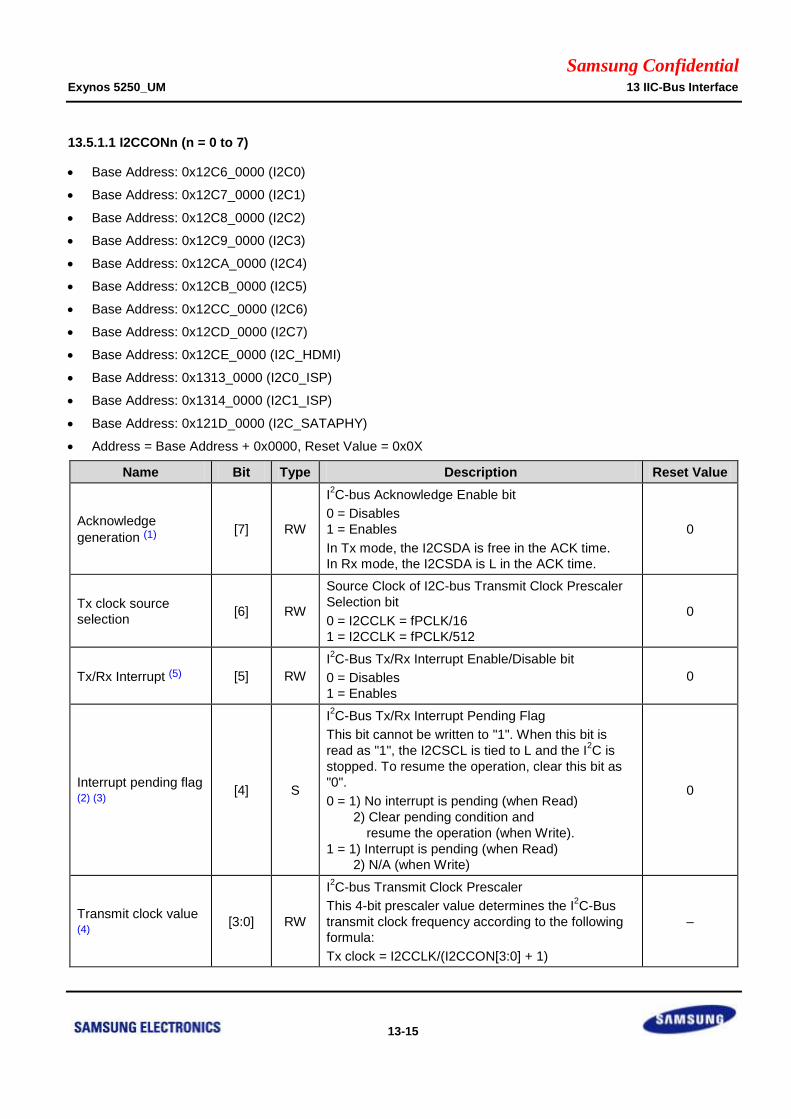
Samsung Confidential Exynos 5250_UM 13 IIC-Bus Interface
13-15
13.5.1.1 I2CCONn (n = 0 to 7)
Base Address: 0x12C6_0000 (I2C0)
Base Address: 0x12C7_0000 (I2C1)
Base Address: 0x12C8_0000 (I2C2)
Base Address: 0x12C9_0000 (I2C3)
Base Address: 0x12CA_0000 (I2C4)
Base Address: 0x12CB_0000 (I2C5)
Base Address: 0x12CC_0000 (I2C6)
Base Address: 0x12CD_0000 (I2C7)
Base Address: 0x12CE_0000 (I2C_HDMI)
Base Address: 0x1313_0000 (I2C0_ISP)
Base Address: 0x1314_0000 (I2C1_ISP)
Base Address: 0x121D_0000 (I2C_SATAPHY)
Address = Base Address + 0x0000, Reset Value = 0x0X
Name Bit Type Description Reset Value
Acknowledge
generation (1) [7] RW
I2C-bus Acknowledge Enable bit
0 = Disables
1 = Enables
In Tx mode, the I2CSDA is free in the ACK time.
In Rx mode, the I2CSDA is L in the ACK time.
0
Tx clock source
selection [6] RW
Source Clock of I2C-bus Transmit Clock Prescaler
Selection bit
0 = I2CCLK = fPCLK/16
1 = I2CCLK = fPCLK/512
0
Tx/Rx Interrupt (5) [5] RW
I2C-Bus Tx/Rx Interrupt Enable/Disable bit
0 = Disables
1 = Enables
0
Interrupt pending flag (2) (3)
[4] S
I2C-Bus Tx/Rx Interrupt Pending Flag
This bit cannot be written to "1". When this bit is
read as "1", the I2CSCL is tied to L and the I2C is
stopped. To resume the operation, clear this bit as
"0".
0 = 1) No interrupt is pending (when Read)
2) Clear pending condition and
resume the operation (when Write).
1 = 1) Interrupt is pending (when Read)
2) N/A (when Write)
0
Transmit clock value (4)
[3:0] RW
I2C-bus Transmit Clock Prescaler
This 4-bit prescaler value determines the I2C-Bus
transmit clock frequency according to the following
formula:
Tx clock = I2CCLK/(I2CCON[3:0] + 1)
–
Samsung Confidential Exynos 5250_UM 13 IIC-Bus Interface
13-16
NOTE:
1 While interfacing with EEPROM, the ACK generation may be disabled before reading the last data to generate the STOP
condition in Rx mode.
2. An I2C-Bus interrupt occurs when:
1) A 1-byte transmit or receive operation is complete. Alternatively, ACK period is finished.
2) A general call or a slave address match occurs.
3) Bus arbitration fails.
3. To adjust the setup time of SDA before SCL rising edge, I2CDS should be written before clearing the I2C interrupt
pending bit.
4. I2CCLK is determined by I2CCON[6].
Tx clock can vary by SCL transition time. When I2CCON[6] = 0, I2CCON[3:0] = 0x0 or 0x1 is not available.
5. When the I2CCON[5] = 0, I2CCON[4] does not operate correctly.
Therefore, It is recommended to set I2CCON[5] = 1, even when you do not use the I2C interrupt.
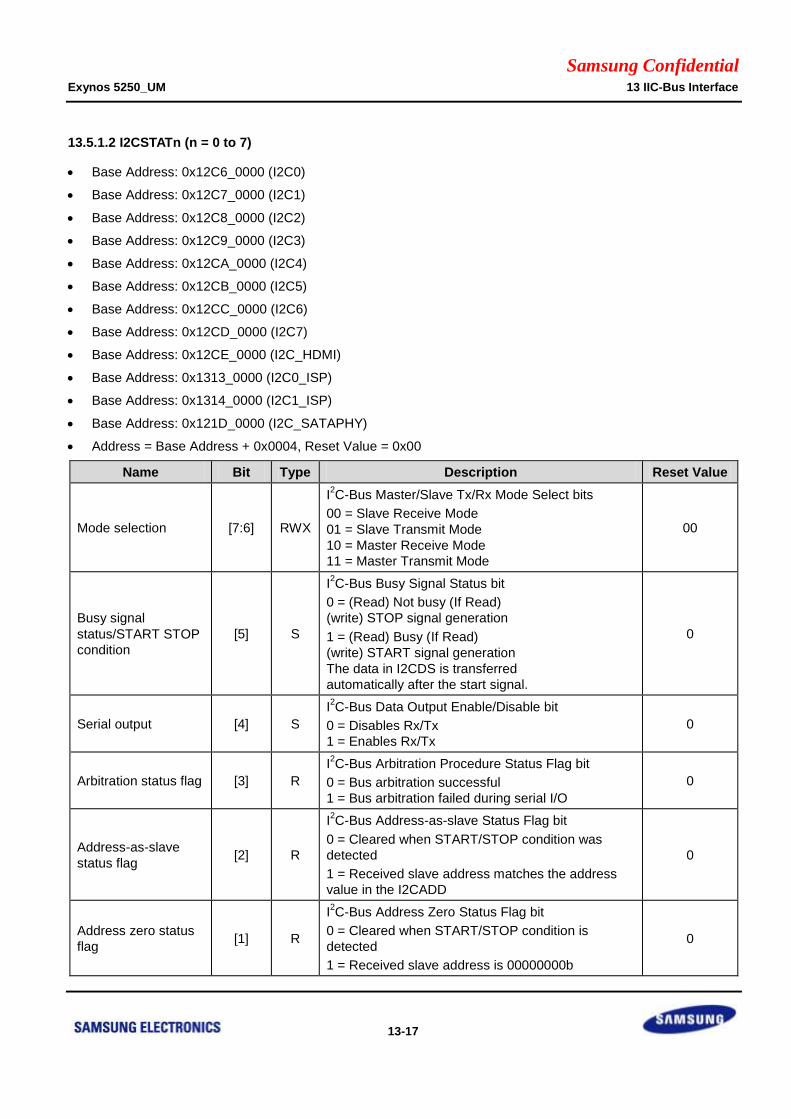
Samsung Confidential Exynos 5250_UM 13 IIC-Bus Interface
13-17
13.5.1.2 I2CSTATn (n = 0 to 7)
Base Address: 0x12C6_0000 (I2C0)
Base Address: 0x12C7_0000 (I2C1)
Base Address: 0x12C8_0000 (I2C2)
Base Address: 0x12C9_0000 (I2C3)
Base Address: 0x12CA_0000 (I2C4)
Base Address: 0x12CB_0000 (I2C5)
Base Address: 0x12CC_0000 (I2C6)
Base Address: 0x12CD_0000 (I2C7)
Base Address: 0x12CE_0000 (I2C_HDMI)
Base Address: 0x1313_0000 (I2C0_ISP)
Base Address: 0x1314_0000 (I2C1_ISP)
Base Address: 0x121D_0000 (I2C_SATAPHY)
Address = Base Address + 0x0004, Reset Value = 0x00
Name Bit Type Description Reset Value
Mode selection [7:6] RWX
I2C-Bus Master/Slave Tx/Rx Mode Select bits
00 = Slave Receive Mode
01 = Slave Transmit Mode
10 = Master Receive Mode
11 = Master Transmit Mode
00
Busy signal
status/START STOP
condition
[5] S
I2C-Bus Busy Signal Status bit
0 = (Read) Not busy (If Read)
(write) STOP signal generation
1 = (Read) Busy (If Read)
(write) START signal generation
The data in I2CDS is transferred
automatically after the start signal.
0
Serial output [4] S
I2C-Bus Data Output Enable/Disable bit
0 = Disables Rx/Tx
1 = Enables Rx/Tx
0
Arbitration status flag [3] R
I2C-Bus Arbitration Procedure Status Flag bit
0 = Bus arbitration successful
1 = Bus arbitration failed during serial I/O
0
Address-as-slave
status flag [2] R
I2C-Bus Address-as-slave Status Flag bit
0 = Cleared when START/STOP condition was
detected
1 = Received slave address matches the address
value in the I2CADD
0
Address zero status
flag [1] R
I2C-Bus Address Zero Status Flag bit
0 = Cleared when START/STOP condition is
detected
1 = Received slave address is 00000000b
0
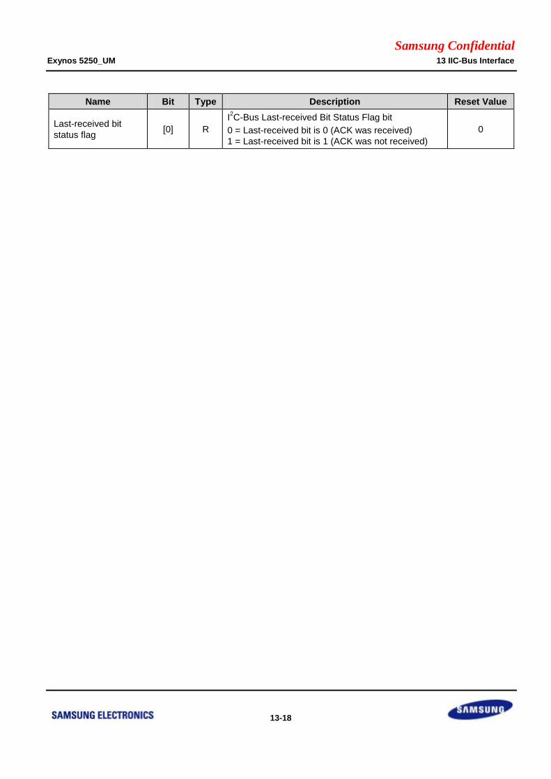
Samsung Confidential Exynos 5250_UM 13 IIC-Bus Interface
13-18
Name Bit Type Description Reset Value
Last-received bit
status flag [0] R
I2C-Bus Last-received Bit Status Flag bit
0 = Last-received bit is 0 (ACK was received)
1 = Last-received bit is 1 (ACK was not received)
0
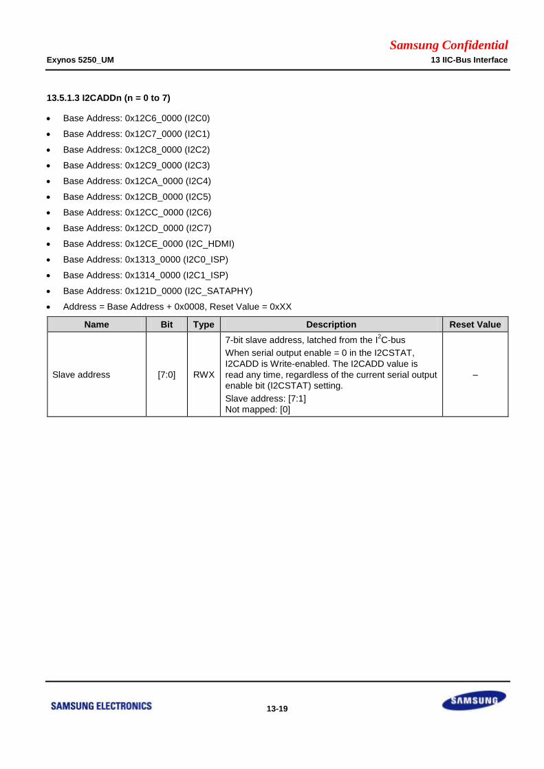
Samsung Confidential Exynos 5250_UM 13 IIC-Bus Interface
13-19
13.5.1.3 I2CADDn (n = 0 to 7)
Base Address: 0x12C6_0000 (I2C0)
Base Address: 0x12C7_0000 (I2C1)
Base Address: 0x12C8_0000 (I2C2)
Base Address: 0x12C9_0000 (I2C3)
Base Address: 0x12CA_0000 (I2C4)
Base Address: 0x12CB_0000 (I2C5)
Base Address: 0x12CC_0000 (I2C6)
Base Address: 0x12CD_0000 (I2C7)
Base Address: 0x12CE_0000 (I2C_HDMI)
Base Address: 0x1313_0000 (I2C0_ISP)
Base Address: 0x1314_0000 (I2C1_ISP)
Base Address: 0x121D_0000 (I2C_SATAPHY)
Address = Base Address + 0x0008, Reset Value = 0xXX
Name Bit Type Description Reset Value
Slave address [7:0] RWX
7-bit slave address, latched from the I2C-bus
When serial output enable = 0 in the I2CSTAT,
I2CADD is Write-enabled. The I2CADD value is
read any time, regardless of the current serial output
enable bit (I2CSTAT) setting.
Slave address: [7:1]
Not mapped: [0]
–
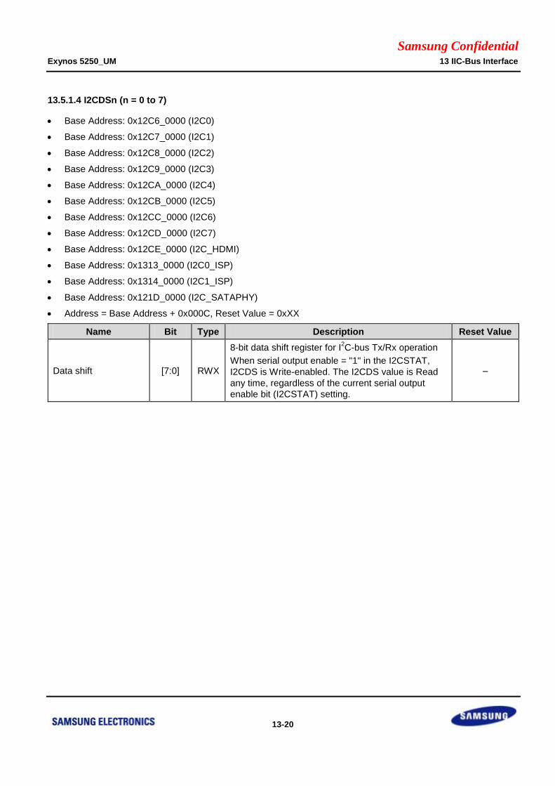
Samsung Confidential Exynos 5250_UM 13 IIC-Bus Interface
13-20
13.5.1.4 I2CDSn (n = 0 to 7)
Base Address: 0x12C6_0000 (I2C0)
Base Address: 0x12C7_0000 (I2C1)
Base Address: 0x12C8_0000 (I2C2)
Base Address: 0x12C9_0000 (I2C3)
Base Address: 0x12CA_0000 (I2C4)
Base Address: 0x12CB_0000 (I2C5)
Base Address: 0x12CC_0000 (I2C6)
Base Address: 0x12CD_0000 (I2C7)
Base Address: 0x12CE_0000 (I2C_HDMI)
Base Address: 0x1313_0000 (I2C0_ISP)
Base Address: 0x1314_0000 (I2C1_ISP)
Base Address: 0x121D_0000 (I2C_SATAPHY)
Address = Base Address + 0x000C, Reset Value = 0xXX
Name Bit Type Description Reset Value
Data shift [7:0] RWX
8-bit data shift register for I2C-bus Tx/Rx operation
When serial output enable = "1" in the I2CSTAT,
I2CDS is Write-enabled. The I2CDS value is Read
any time, regardless of the current serial output
enable bit (I2CSTAT) setting.
–
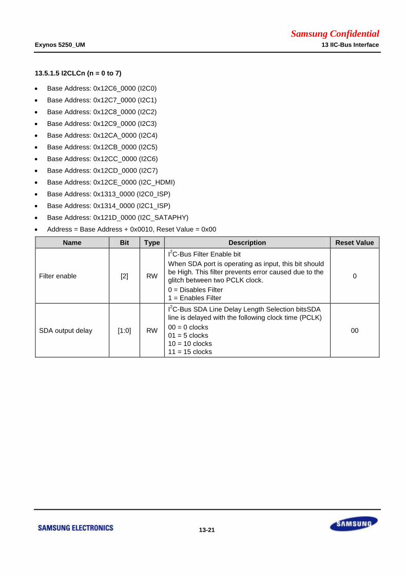
Samsung Confidential Exynos 5250_UM 13 IIC-Bus Interface
13-21
13.5.1.5 I2CLCn (n = 0 to 7)
Base Address: 0x12C6_0000 (I2C0)
Base Address: 0x12C7_0000 (I2C1)
Base Address: 0x12C8_0000 (I2C2)
Base Address: 0x12C9_0000 (I2C3)
Base Address: 0x12CA_0000 (I2C4)
Base Address: 0x12CB_0000 (I2C5)
Base Address: 0x12CC_0000 (I2C6)
Base Address: 0x12CD_0000 (I2C7)
Base Address: 0x12CE_0000 (I2C_HDMI)
Base Address: 0x1313_0000 (I2C0_ISP)
Base Address: 0x1314_0000 (I2C1_ISP)
Base Address: 0x121D_0000 (I2C_SATAPHY)
Address = Base Address + 0x0010, Reset Value = 0x00
Name Bit Type Description Reset Value
Filter enable [2] RW
I2C-Bus Filter Enable bit
When SDA port is operating as input, this bit should
be High. This filter prevents error caused due to the
glitch between two PCLK clock.
0 = Disables Filter
1 = Enables Filter
0
SDA output delay [1:0] RW
I2C-Bus SDA Line Delay Length Selection bitsSDA
line is delayed with the following clock time (PCLK)
00 = 0 clocks
01 = 5 clocks
10 = 10 clocks
11 = 15 clocks
00
Samsung Confidential Exynos 5250_UM 14 Serial Peripheral Interface
14-1
14 Serial Peripheral Interface
14.1 Overview
Serial Peripheral Interface (SPI) in Exynos 5250 transfers serial data by using various peripherals.
SPI includes two 8, 16, 32-bit shift registers to transmit and receive data. It transfers (shifts out serially) and
receives (shifts in serially) data simultaneously. It supports the protocols for National Semiconductor Microwire
and Motorola Serial Peripheral Interface.
14.2 Features
Features of SPI are:
Supports full duplex
Supports 8/16/32-bit shift register for Tx/Rx
Supports 8-bit/16-bit/32-bit bus interface
Supports the Motorola SPI protocol and National Semiconductor Microwire
Supports two independent 32-bit wide transmit and receive FIFOs:
Depth 64 in SPI port 0 and depth 16 in SPI port 1 and 2
Depth 64 in ISP-SPI port 0 and 1
Supports Master-mode and Slave-mode
Supports Receive-without-transmit operation
Supports Tx/Rx maximum frequency at up to 50 MHz
Samsung Confidential Exynos 5250_UM 14 Serial Peripheral Interface
14-2
14.2.1 Operation of Serial Peripheral Interface
SPI transfers 1-bit serial data between Exynos 5250 and external device. SPI in Exynos 5250 supports CPU or
DMA to transmit or receive FIFOs separately. It also supports to transfer data in both directions simultaneously.
SPI has two channels: Tx channel and Rx channel. The Tx channel has the path from Tx FIFO to external device.
The Rx channel has the path from external device to Rx FIFO.
CPU or DMA must write data on the register SPI_TX_DATA, to write data in FIFO. Data on the register are
automatically moved to Tx FIFOs. To read data from Rx FIFOs, CPU or DMA must access the SPI_RX_DATA
register and data are automatically sent to the SPI_RX_DATA register.
CMU registers controls the SPI operating frequency. Refer to Chapter 7 Clock Controller for more information.
14.2.1.1 Operation Mode
SPI has two modes:
Master mode
Slave mode
In master mode, SPICLK is generated and transmitted to external device. The signal to select the slave, XspiCS#,
indicates that the data is valid when XspiCS# is set to low level. XspiCS# must be set low level before packets are
transmitted or received.
14.2.1.2 FIFO Access
SPI supports CPU and DMA access to FIFOs. Data size of CPU access and DMA access to FIFOs is selected
either from 8-bit, 16-bit, or 32-bit data. When 8-bit data size is selected, valid bits are from 0-bit to 7-bit. User can
define the trigger threshold to raise interrupt to CPU. The trigger level of each FIFO in port 0 is set by 4 bytes step
from 0 byte to 252 bytes. Each FIFO in port 1 is set by 1 byte step from 0 byte to 63 bytes. TxDMAOn or
RxDMAOn bit of SPI_MODE_CFG register must be set to use DMA access. DMA access supports only single
transfer and 4-burst transfer. In Tx FIFO, DMA request signal is high until Tx FIFO is full. In Rx FIFO, DMA
request signal is high when Rx FIFO is not empty.
14.2.1.3 Trailing Bytes in the Rx FIFO
Trailing bytes are the remaining bytes when the number of samples in Rx FIFO is less than the threshold value in
INT or DMA 4 burst mode and when no additional data is received. To remove these bytes in Rx FIFO, It uses
internal timer and interrupt signal. The value of internal timer is set to 1024 clocks based on APB BUS clock.
When timer value is set to zero, interrupt signal occurs and CPU can eliminate trailing bytes in FIFO.
Samsung Confidential Exynos 5250_UM 14 Serial Peripheral Interface
14-3
14.2.1.4 Packet Number Control
SPI controls the number of packets to be received in master mode. Set SFR (PACKET_CNT_REG) to receive any
number of packets. SPI stops generating SPICLK when the number of packets is the same as
PACKET_CNT_REG. The size of one packet depends on channel width.
NOTE: One packet is 1 byte if channel width is configured as byte, and one packet is 4 bytes if channel width is configured as
word. Mandatorily follow software or hardware reset before this function is reloaded.
Software reset clears all registers except special function registers. However, hardware reset clears all registers.
14.2.1.5 Chip Select Control
Chip select XspiCS# is active in low signal. Alternatively, a chip is selected when XspiCS# input is 0.
You can control XspiCS# automatically or manually.
When you use manual control mode, AUTO_N_MANUAL must be cleared (Default value is 0). NSSOUT bit
controls the XspiCS# level.
When you use auto control mode, AUTO_N_MANUAL must be set to 1. XspiCS toggles between packets
automatically. NCS_TIME_COUNT controls inactive period of XspiCS. NSSOUT is not available at this time.
14.2.1.6 High Speed Operation as Slave
Exynos 5250 SPI supports Tx/Rx operations up to 50 MHz. However, there is a limitation. When Exynos 5250 SPI
works as a slave, there is a delay of more than 15 ns in worst operating condition. Such a large delay can cause
setup violation at the SPI master device. To resolve this problem, Exynos 5250 SPI provides fast slave Tx mode
by setting 1 to HIGH_SPEED bit of CH_CFG register. In this mode, MISO output delay is reduced by half cycle so
that the SPI master device has more setup margin.
However, the fast slave Tx mode can be used only when CPHA = 0.
Samsung Confidential Exynos 5250_UM 14 Serial Peripheral Interface
14-4
14.2.1.7 Feed Back Clock Selection
Under SPI protocol spec, SPI master should capture the input data launched by slave (MISO) with its internal
SPICLK.
When SPI runs at high operating frequency such as 50 MHz, it is difficult to capture the MISO input because the
required arrival time of MISO, which is an half cycle period in Exynos 5250, is shorter than the arrival time of
MISO that consists of SPICLK output delay of SPI master, MISO output delay of SPI slave, and MISO input delay
of SPI master. To resolve this problem, Exynos 5250 SPI provides three feedback clocks that are phase-delayed
clock of internal SPICLK.
A selection of feedback clock depends on MISO output delay of SPI slave. To capture MISO data correctly, it
selects the feedback clock that satisfies this constraint:
tSPIMIS (s) < tperiod/2-tSPISOD
* tSPIMIS (s): MISO input setup time of SPI master on a given feedback clock selection 's'
* tSPISOD: MISO output delay of SPI slave
* tperiod: SPICLK cycle period
When multiple feedback clocks meet the constraint, it selects the feedback clock with smallest phase delay. It is
because a feedback clock with large phase delay may capture data of next cycle.
For example, Exynos 5250 SPI CH1 with master configuration of 50 MHz operating frequency with1.8 V external
voltage and 15 pF load, 270 degree phase-delayed feedback clock should be used when the MISO output delay
of SPI slave is assumed as 11 ns (tSPIMIS (s) < 10 ns – 11 ns = – 1 ns).
When the operating clock frequency is 33 MHz and other conditions are the same as the previous example, then it
is better to use 180 degree phase-delayed feedback clock (tSPIMIS (s) < 15 ns – 11 ns = 4 ns).

Samsung Confidential Exynos 5250_UM 14 Serial Peripheral Interface
14-5
14.2.1.8 SPI Transfer Format
Exynos 5250 supports four different formats for data transfer. Figure 14-1 illustrates four waveforms for SPICLK.
Figure 14-1 SPI Transfer Format
Cycle
MOSI
1 2 3 4 5 6 7 8
MSB 6 5 4 3 2 1 LSB
6 5 4 3 2 1 LSB
SPICLK
MISO MSB
CPOL = 1, CPHA = 1 (Format B)
Cycle
MOSI
1 2 3 4 5 6 7 8
MSB 6 5 4 3 2 1 LSB
6 5 4 3 2 1 LSB *MSB
SPICLK
MISO MSB
CPOL = 1, CPHA = 0 (Format A)
Cycle
MOSI
1 2 3 4 5 6 7 8
6 5 4 3 2 1 LSB
6 5 4 3 2 1 LSB
SPICLK
MISO LSB*
CPOL = 0, CPHA = 1 (Format B)
Cycle
MOSI
1 2 3 4 5 6 7 8
MSB 6 5 4 3 2 1 LSB
6 5 4 3 2 1 LSB *MSB
SPICLK
MISO MSB
CPOL = 0, CPHA = 0 (Format A)
LSB*
MSB
MSB
*MSB : MSB of previous frame
LSB* : LSB of next frame
LSB* : LSB of next frame
*MSB : MSB of previous frame
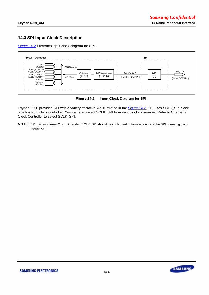
Samsung Confidential Exynos 5250_UM 14 Serial Peripheral Interface
14-6
14.3 SPI Input Clock Description
Figure 14-2 illustrates input clock diagram for SPI.
System Controller
DIVSPI0~2
(1~16)
MUXSPI0~2
MOUTSPI0~2
XXTI
XusbXTI
SCLK_HDMI27M
SCLK_USBPHY0
SCLK_USBPHY1
SCLK_HDMIPHY
SCLKMPLL
SCLKEPLL
SCLKVPLL
SPI_CLKDIV
(2)
SPI
SCLK_SPI
( Max 100MHz )( Max 50MHz )
DIVSPI0~2_PRE
(1~256)
Figure 14-2 Input Clock Diagram for SPI
Exynos 5250 provides SPI with a variety of clocks. As illustrated in the Figure 14-2, SPI uses SCLK_SPI clock,
which is from clock controller. You can also select SCLK_SPI from various clock sources. Refer to Chapter 7
Clock Controller to select SCLK_SPI.
NOTE: SPI has an internal 2x clock divider. SCLK_SPI should be configured to have a double of the SPI operating clock
frequency.
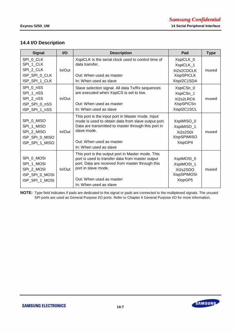
Samsung Confidential Exynos 5250_UM 14 Serial Peripheral Interface
14-7
14.4 I/O Description
Signal I/O Description Pad Type
SPI_0_CLK
SPI_1_CLK
SPI_2_CLK
ISP_SPI_0_CLK
ISP_SPI_1_CLK
In/Out
XspiCLK is the serial clock used to control time of
data transfer.
Out: When used as master
In: When used as slave
XspiCLK_0
XspiCLK_1
Xi2s2CDCLK
XispSPICLK
XispI2C1SDA
muxed
SPI_0_nSS
SPI_1_nSS
SPI_2_nSS
ISP_SPI_0_nSS
ISP_SPI_1_nSS
In/Out
Slave selection signal. All data Tx/Rx sequences
are executed when XspiCS is set to low.
Out: When used as master
In: When used as slave
XspiCSn_0
XspiCSn_1
Xi2s2LRCK
XispSPICSn
XispI2C1SCL
muxed
SPI_0_MISO
SPI_1_MISO
SPI_2_MISO
ISP_SPI_0_MISO
ISP_SPI_1_MISO
In/Out
This port is the input port in Master mode. Input
mode is used to obtain data from slave output port.
Data are transmitted to master through this port in
slave mode.
Out: When used as master
In: When used as slave
XspiMISO_0
XspiMISO_1
Xi2s2SDI
XispSPIMISO
XispGP4
muxed
SPI_0_MOSI
SPI_1_MOSI
SPI_2_MOSI
ISP_SPI_0_MOSI
ISP_SPI_1_MOSI
In/Out
This port is the output port in Master mode. This
port is used to transfer data from master output
port. Data are received from master through this
port in slave mode.
Out: When used as master
In: When used as slave
XspiMOSI_0
XspiMOSI_1
Xi2s2SDO
XispSPIMOSI
XispGP5
muxed
NOTE: Type field indicates if pads are dedicated to the signal or pads are connected to the multiplexed signals. The unused
SPI ports are used as General Purpose I/O ports. Refer to Chapter 6 General Purpose I/O for more information.
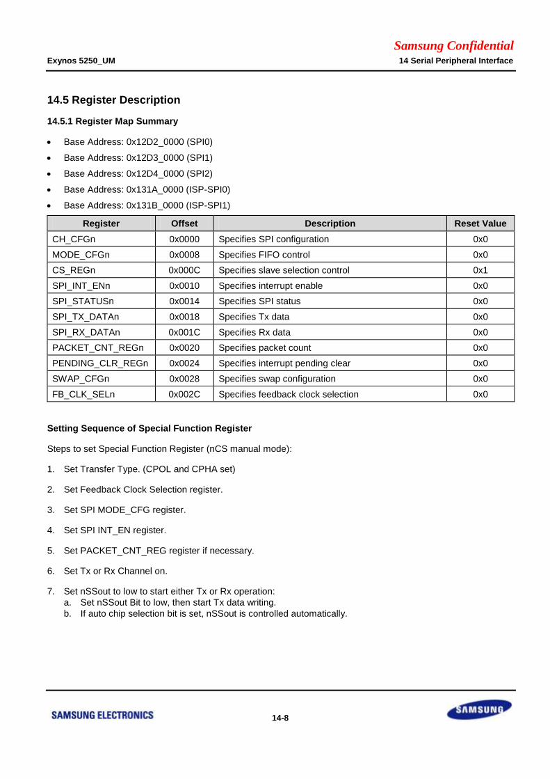
Samsung Confidential Exynos 5250_UM 14 Serial Peripheral Interface
14-8
14.5 Register Description
14.5.1 Register Map Summary
Base Address: 0x12D2_0000 (SPI0)
Base Address: 0x12D3_0000 (SPI1)
Base Address: 0x12D4_0000 (SPI2)
Base Address: 0x131A_0000 (ISP-SPI0)
Base Address: 0x131B_0000 (ISP-SPI1)
Register Offset Description Reset Value
CH_CFGn 0x0000 Specifies SPI configuration 0x0
MODE_CFGn 0x0008 Specifies FIFO control 0x0
CS_REGn 0x000C Specifies slave selection control 0x1
SPI_INT_ENn 0x0010 Specifies interrupt enable 0x0
SPI_STATUSn 0x0014 Specifies SPI status 0x0
SPI_TX_DATAn 0x0018 Specifies Tx data 0x0
SPI_RX_DATAn 0x001C Specifies Rx data 0x0
PACKET_CNT_REGn 0x0020 Specifies packet count 0x0
PENDING_CLR_REGn 0x0024 Specifies interrupt pending clear 0x0
SWAP_CFGn 0x0028 Specifies swap configuration 0x0
FB_CLK_SELn 0x002C Specifies feedback clock selection 0x0
Setting Sequence of Special Function Register
Steps to set Special Function Register (nCS manual mode):
1. Set Transfer Type. (CPOL and CPHA set)
2. Set Feedback Clock Selection register.
3. Set SPI MODE_CFG register.
4. Set SPI INT_EN register.
5. Set PACKET_CNT_REG register if necessary.
6. Set Tx or Rx Channel on.
7. Set nSSout to low to start either Tx or Rx operation:
a. Set nSSout Bit to low, then start Tx data writing.
b. If auto chip selection bit is set, nSSout is controlled automatically.
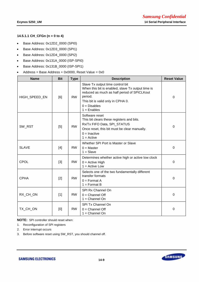
Samsung Confidential Exynos 5250_UM 14 Serial Peripheral Interface
14-9
14.5.1.1 CH_CFGn (n = 0 to 4)
Base Address: 0x12D2_0000 (SPI0)
Base Address: 0x12D3_0000 (SPI1)
Base Address: 0x12D4_0000 (SPI2)
Base Address: 0x131A_0000 (ISP-SPI0)
Base Address: 0x131B_0000 (ISP-SPI1)
Address = Base Address + 0x0000, Reset Value = 0x0
Name Bit Type Description Reset Value
HIGH_SPEED_EN [6] RW
Slave Tx output time control bit
When this bit is enabled, slave Tx output time is
reduced as much as half period of SPICLKout
period.
This bit is valid only in CPHA 0.
0 = Disables
1 = Enables
0
SW_RST [5] RW
Software reset
This bit clears these registers and bits.
Rx/Tx FIFO Data, SPI_STATUS
Once reset, this bit must be clear manually.
0 = Inactive
1 = Active
0
SLAVE [4] RW
Whether SPI Port is Master or Slave
0 = Master
1 = Slave
0
CPOL [3] RW
Determines whether active high or active low clock
0 = Active High
1 = Active Low
0
CPHA [2] RW
Selects one of the two fundamentally different
transfer formats
0 = Format A
1 = Format B
0
RX_CH_ON [1] RW
SPI Rx Channel On
0 = Channel Off
1 = Channel On
0
TX_CH_ON [0] RW
SPI Tx Channel On
0 = Channel Off
1 = Channel On
0
NOTE: SPI controller should reset when:
1. Reconfiguration of SPI registers
2. Error interrupt occurs
3. Before software reset using SW_RST, you should channel off.
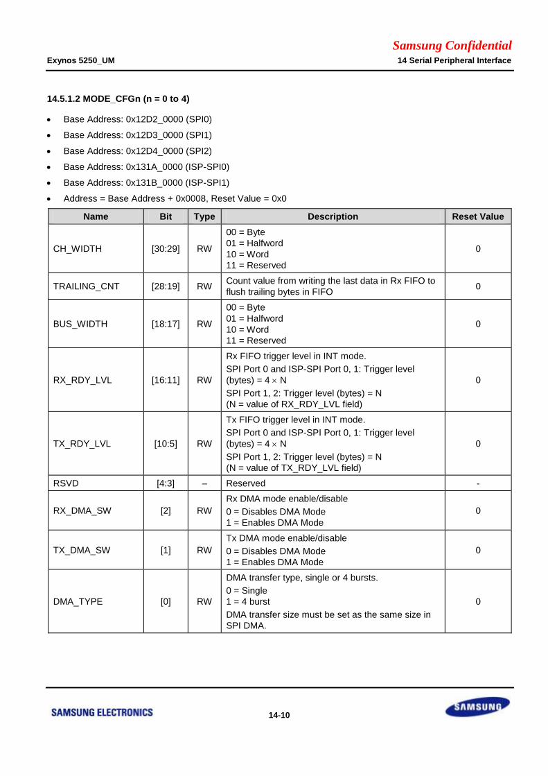
Samsung Confidential Exynos 5250_UM 14 Serial Peripheral Interface
14-10
14.5.1.2 MODE_CFGn (n = 0 to 4)
Base Address: 0x12D2_0000 (SPI0)
Base Address: 0x12D3_0000 (SPI1)
Base Address: 0x12D4_0000 (SPI2)
Base Address: 0x131A_0000 (ISP-SPI0)
Base Address: 0x131B_0000 (ISP-SPI1)
Address = Base Address + 0x0008, Reset Value = 0x0
Name Bit Type Description Reset Value
CH_WIDTH [30:29] RW
00 = Byte
01 = Halfword
10 = Word
11 = Reserved
0
TRAILING_CNT [28:19] RW Count value from writing the last data in Rx FIFO to
flush trailing bytes in FIFO 0
BUS_WIDTH [18:17] RW
00 = Byte
01 = Halfword
10 = Word
11 = Reserved
0
RX_RDY_LVL [16:11] RW
Rx FIFO trigger level in INT mode.
SPI Port 0 and ISP-SPI Port 0, 1: Trigger level
(bytes) = 4 N
SPI Port 1, 2: Trigger level (bytes) = N
(N = value of RX_RDY_LVL field)
0
TX_RDY_LVL [10:5] RW
Tx FIFO trigger level in INT mode.
SPI Port 0 and ISP-SPI Port 0, 1: Trigger level
(bytes) = 4 N
SPI Port 1, 2: Trigger level (bytes) = N
(N = value of TX_RDY_LVL field)
0
RSVD [4:3] – Reserved -
RX_DMA_SW [2] RW
Rx DMA mode enable/disable
0 = Disables DMA Mode
1 = Enables DMA Mode
0
TX_DMA_SW [1] RW
Tx DMA mode enable/disable
0 = Disables DMA Mode
1 = Enables DMA Mode
0
DMA_TYPE [0] RW
DMA transfer type, single or 4 bursts.
0 = Single
1 = 4 burst
DMA transfer size must be set as the same size in
SPI DMA.
0
Samsung Confidential Exynos 5250_UM 14 Serial Peripheral Interface
14-11
NOTE:
1. CH_WIDTH is shift-register width.
2. BUS_WIDTH is SPI FIFO width. The transfer data size should be aligned with BUS_WIDTH.
For example, TX/RX data size must be aligned with 4 bytes if BUS_WIDTH is word.
3. CH_WIDTH must be smaller than BUS_WIDTH or same.
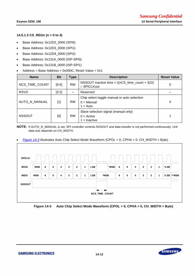
Samsung Confidential Exynos 5250_UM 14 Serial Peripheral Interface
14-12
14.5.1.3 CS_REGn (n = 0 to 4)
Base Address: 0x12D2_0000 (SPI0)
Base Address: 0x12D3_0000 (SPI1)
Base Address: 0x12D4_0000 (SPI2)
Base Address: 0x131A_0000 (ISP-SPI0)
Base Address: 0x131B_0000 (ISP-SPI1)
Address = Base Address + 0x000C, Reset Value = 0x1
Name Bit Type Description Reset Value
NCS_TIME_COUNT [9:4] RW NSSOUT inactive time = ((nCS_time_count + 3)/2)
SPICLKout 0
RSVD [3:2] – Reserved –
AUTO_N_MANUAL [1] RW
Chip select toggle manual or auto selection
0 = Manual
1 = Auto
0
NSSOUT [0] RW
Slave selection signal (manual only)
0 = Active
1 = Inactive
1
NOTE: If AUTO_N_MANUAL is set, SPI controller controls NSSOUT and data transfer is not performed continuously. Unit
data size depends on CH_WIDTH.
Figure 14-3 illustrates Auto Chip Select Mode Waveform (CPOL = 0, CPHA = 0, CH_WIDTH = Byte).
Figure 14-3 Auto Chip Select Mode Waveform (CPOL = 0, CPHA = 0, CH_WIDTH = Byte)
SPICLK
MOSI MSB 6 5 4 3 2 1 LSB
MSB 6 5 4 3 2 1 LSB *MSBMISO
NSSOUT
*MSB 6 5 4 3 2 1 *LSB
6 5 4 3 2 1 *LSB **MSB
NCS_TIME_COUNT
Samsung Confidential Exynos 5250_UM 14 Serial Peripheral Interface
14-13
14.5.1.4 SPI_INT_ENn (n = 0 to 4)
Base Address: 0x12D2_0000 (SPI0)
Base Address: 0x12D3_0000 (SPI1)
Base Address: 0x12D4_0000 (SPI2)
Base Address: 0x131A_0000 (ISP-SPI0)
Base Address: 0x131B_0000 (ISP-SPI1)
Address = Base Address + 0x0010, Reset Value = 0x0
Name Bit Type Description Reset Value
INT_EN_TRAILING [6] RW
Interrupt Enable for trailing count to be 0
0 = Disables interrupt
1 = Enables interrupt
0
INT_EN_RX_OVER
RUN [5] RW
Interrupt Enable for RxOverrun
0 = Disables interrupt
1 = Enables interrupt
0
INT_EN_RX_UNDE
RRUN [4] RW
Interrupt Enable for RxUnderrun
0 = Disables interrupt
1 = Enables interrupt
0
INT_EN_TX_OVER
RUN [3] RW
Interrupt Enable for TxOverrun
0 = Disables interrupt
1 = Enables interrupt
0
INT_EN_TX_UNDE
RRUN [2] RW
Interrupt Enable for TxUnderrun. In slave mode, this
bit must be clear first after turning on slave Tx path.
0 = Disables interrupt
1 = Enables interrupt
0
INT_EN_RX_FIFO_
RDY [1] RW
Interrupt Enable for RxFifoRdy (INT mode)
0 = Disables interrupt
1 = Enables interrupt
0
INT_EN_TX_FIFO_
RDY [0] RW
Interrupt Enable for TxFifoRdy (INT mode)
0 = Disables interrupt
1 = Enables interrupt
0
Samsung Confidential Exynos 5250_UM 14 Serial Peripheral Interface
14-14
14.5.1.5 SPI_STATUSn (n = 0 to 4)
Base Address: 0x12D2_0000 (SPI0)
Base Address: 0x12D3_0000 (SPI1)
Base Address: 0x12D4_0000 (SPI2)
Base Address: 0x131A_0000 (ISP-SPI0)
Base Address: 0x131B_0000 (ISP-SPI1)
Address = Base Address + 0x0014, Reset Value = 0x0
Name Bit Type Description Reset Value
TX_DONE [25] R
Indication of transfer done in Shift register (master
mode only)
0 = All case except Tx FIFO and shift register case
1 = When Tx FIFO and shift register are empty after
transmission start
0
TRAILING_BYTE [24] R Indication that trailing count is 0 0
RX_FIFO_LVL [23:15] R
Data level in Rx FIFO
0 to 256 bytes in port 0
0 to 64 bytes in port 1 and 2
0
TX_FIFO_LVL [14:6] R
Data level in Tx FIFO
0 to 256 bytes in port 0
0 to 64 bytes in port 1 and 2
0
RX_OVERRUN [5] R
Rx FIFO overrun error
0 = No Error
1 = Overrun Error
0
RX_UNDERRUN [4] R
Rx FIFO underrun error
0 = No Error
1 = Underrun Error
0
TX_OVERRUN [3] R
Tx FIFO overrun error
0 = No Error
1 = Overrun Error
0
TX_UNDERRUN [2] R
Tx FIFO underrun error
0 = No Error
1 = Underrun Error
NOTE: Tx FIFO underrun error occurs when Tx
FIFO is empty in slave mode.
0
RX_FIFO_RDY [1] R 0 = Data in FIFO less than trigger level
1 = Data in FIFO more than trigger level 0
TX_FIFO_RDY [0] R 0 = Data in FIFO more than trigger level
1 = Data in FIFO less than trigger level 0
Samsung Confidential Exynos 5250_UM 14 Serial Peripheral Interface
14-15
14.5.1.6 SPI_TX_DATAn (n = 0 to 4)
Base Address: 0x12D2_0000 (SPI0)
Base Address: 0x12D3_0000 (SPI1)
Base Address: 0x12D4_0000 (SPI2)
Base Address: 0x131A_0000 (ISP-SPI0)
Base Address: 0x131B_0000 (ISP-SPI1)
Address = Base Address + 0x0018, Reset Value = 0x0
Name Bit Type Description Reset Value
TX_DATA [31:0] W This field contains the data to be transmitted over
the SPI channel. 0
14.5.1.7 SPI_RX_DATAn (n = 0 to 4)
Base Address: 0x12D2_0000 (SPI0)
Base Address: 0x12D3_0000 (SPI1)
Base Address: 0x12D4_0000 (SPI2)
Base Address: 0x131A_0000 (ISP-SPI0)
Base Address: 0x131B_0000 (ISP-SPI1)
Address = Base Address + 0x001C, Reset Value = 0x0
Name Bit Type Description Reset Value
RX_DATA [31:0] R This field contains the data to be received over the
SPI channel. 0
14.5.1.8 PACKET_CNT_REGn (n = 0 to 4)
Base Address: 0x12D2_0000 (SPI0)
Base Address: 0x12D3_0000 (SPI1)
Base Address: 0x12D4_0000 (SPI2)
Base Address: 0x131A_0000 (ISP-SPI0)
Base Address: 0x131B_0000 (ISP-SPI1)
Address = Base Address + 0x0020, Reset Value = 0x0
Name Bit Type Description Reset Value
PACKET_CNT_EN [16] RW
Enable bit for packet count
0 = Disables
1 = Enables
0
COUNT_VALUE [15:0] RW Packet count value 0
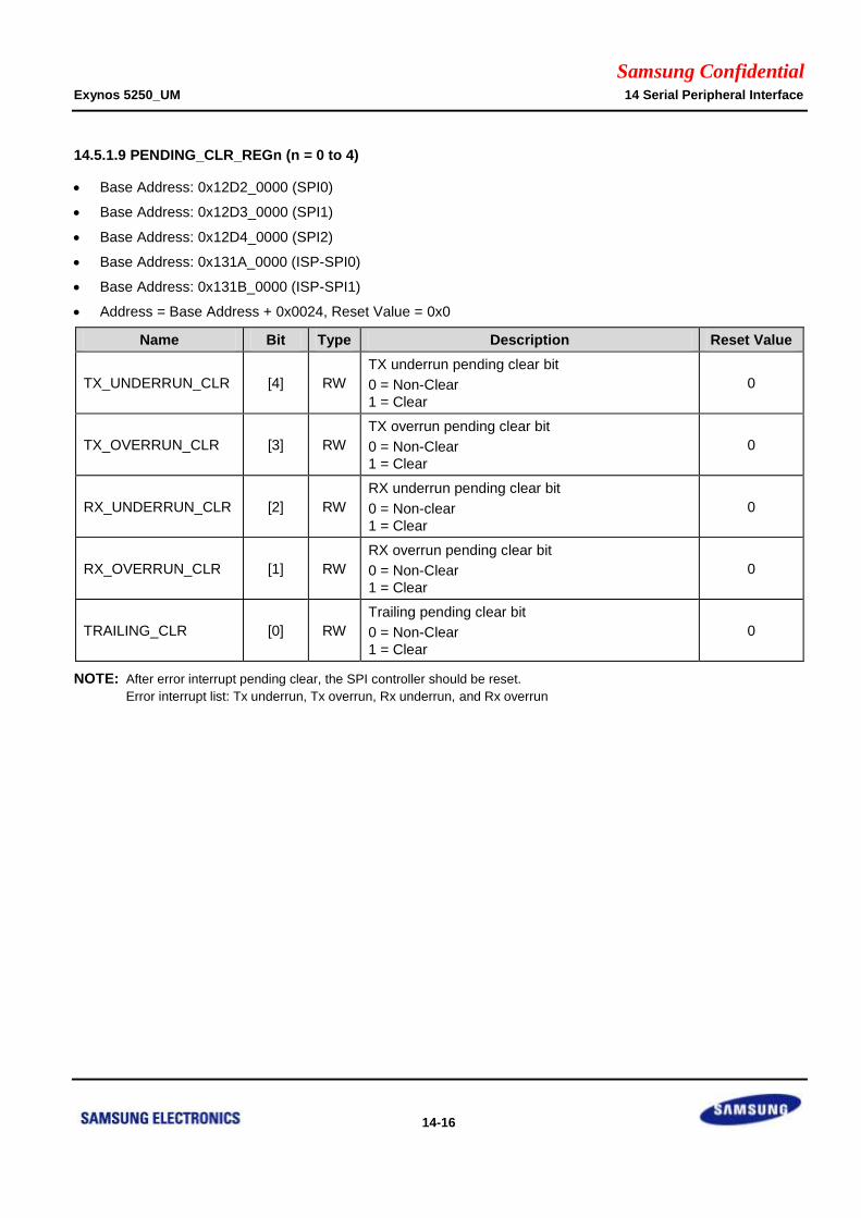
Samsung Confidential Exynos 5250_UM 14 Serial Peripheral Interface
14-16
14.5.1.9 PENDING_CLR_REGn (n = 0 to 4)
Base Address: 0x12D2_0000 (SPI0)
Base Address: 0x12D3_0000 (SPI1)
Base Address: 0x12D4_0000 (SPI2)
Base Address: 0x131A_0000 (ISP-SPI0)
Base Address: 0x131B_0000 (ISP-SPI1)
Address = Base Address + 0x0024, Reset Value = 0x0
Name Bit Type Description Reset Value
TX_UNDERRUN_CLR [4] RW
TX underrun pending clear bit
0 = Non-Clear
1 = Clear
0
TX_OVERRUN_CLR [3] RW
TX overrun pending clear bit
0 = Non-Clear
1 = Clear
0
RX_UNDERRUN_CLR [2] RW
RX underrun pending clear bit
0 = Non-clear
1 = Clear
0
RX_OVERRUN_CLR [1] RW
RX overrun pending clear bit
0 = Non-Clear
1 = Clear
0
TRAILING_CLR [0] RW
Trailing pending clear bit
0 = Non-Clear
1 = Clear
0
NOTE: After error interrupt pending clear, the SPI controller should be reset.
Error interrupt list: Tx underrun, Tx overrun, Rx underrun, and Rx overrun

Samsung Confidential Exynos 5250_UM 14 Serial Peripheral Interface
14-17
14.5.1.10 SWAP_CFGn (n = 0 to 4)
Base Address: 0x12D2_0000 (SPI0)
Base Address: 0x12D3_0000 (SPI1)
Base Address: 0x12D4_0000 (SPI2)
Base Address: 0x131A_0000 (ISP-SPI0)
Base Address: 0x131B_0000 (ISP-SPI1)
Address = Base Address + 0x0028, Reset Value = 0x0
Name Bit Type Description Reset Value
RX_HWORD_SWAP [7] RW 0 = Off
1 = Swap 0
RX_BYTE_SWAP [6] RW 0 = Off
1 = Swap 0
RX_BIT_SWAP [5] RW 0 = Off
1 = Swap 0
RX_SWAP_EN [4] RW
Swap enable
0 = Normal
1 = Swap
0
TX_HWORD_SWAP [3] RW 0 = Off
1 = Swap 0
TX_BYTE_SWAP [2] RW 0 = Off
1 = Swap 0
TX_BIT_SWAP [1] RW 0 = Off
1 = Swap 0
TX_SWAP_EN [0] RW
Swap enable
0 = Normal
1 = Swap
0
NOTE: Data size must be larger than swap size.
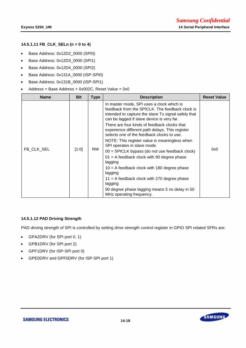
Samsung Confidential Exynos 5250_UM 14 Serial Peripheral Interface
14-18
14.5.1.11 FB_CLK_SELn (n = 0 to 4)
Base Address: 0x12D2_0000 (SPI0)
Base Address: 0x12D3_0000 (SPI1)
Base Address: 0x12D4_0000 (SPI2)
Base Address: 0x131A_0000 (ISP-SPI0)
Base Address: 0x131B_0000 (ISP-SPI1)
Address = Base Address + 0x002C, Reset Value = 0x0
Name Bit Type Description Reset Value
FB_CLK_SEL [1:0] RW
In master mode, SPI uses a clock which is
feedback from the SPICLK. The feedback clock is
intended to capture the slave Tx signal safely that
can be lagged if slave device is very far.
There are four kinds of feedback clocks that
experience different path delays. This register
selects one of the feedback clocks to use.
NOTE: This register value is meaningless when
SPI operates in slave mode.
00 = SPICLK bypass (do not use feedback clock)
01 = A feedback clock with 90 degree phase
lagging
10 = A feedback clock with 180 degree phase
lagging
11 = A feedback clock with 270 degree phase
lagging
90 degree phase lagging means 5 ns delay in 50
MHz operating frequency.
0x0
14.5.1.12 PAD Driving Strength
PAD driving strength of SPI is controlled by setting drive strength control register in GPIO SPI related SFRs are:
GPA2DRV (for SPI port 0, 1)
GPB1DRV (for SPI port 2)
GPF1DRV (for ISP-SPI port 0)
GPE0DRV and GPF0DRV (for ISP-SPI port 1)
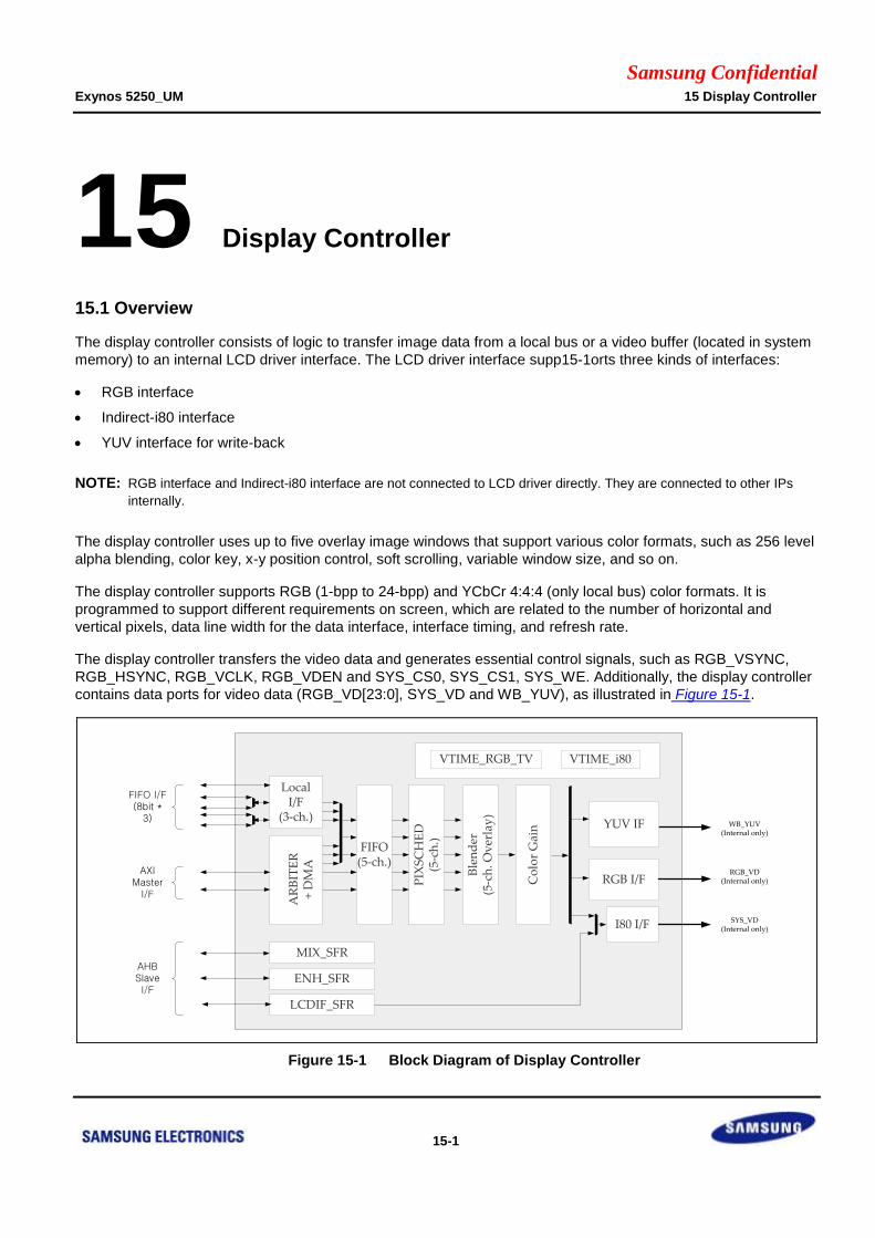
Samsung Confidential Exynos 5250_UM 15 Display Controller
15-1
15 Display Controller
15.1 Overview
The display controller consists of logic to transfer image data from a local bus or a video buffer (located in system
memory) to an internal LCD driver interface. The LCD driver interface supp15-1orts three kinds of interfaces:
RGB interface
Indirect-i80 interface
YUV interface for write-back
NOTE: RGB interface and Indirect-i80 interface are not connected to LCD driver directly. They are connected to other IPs
internally.
The display controller uses up to five overlay image windows that support various color formats, such as 256 level
alpha blending, color key, x-y position control, soft scrolling, variable window size, and so on.
The display controller supports RGB (1-bpp to 24-bpp) and YCbCr 4:4:4 (only local bus) color formats. It is
programmed to support different requirements on screen, which are related to the number of horizontal and
vertical pixels, data line width for the data interface, interface timing, and refresh rate.
The display controller transfers the video data and generates essential control signals, such as RGB_VSYNC,
RGB_HSYNC, RGB_VCLK, RGB_VDEN and SYS_CS0, SYS_CS1, SYS_WE. Additionally, the display controller
contains data ports for video data (RGB_VD[23:0], SYS_VD and WB_YUV), as illustrated in Figure 15-1.
PIX
SC
HE
D(5
-ch
.)
Ble
nd
er(5
-ch
. Ov
erla
y)
VTIME_RGB_TV VTIME_i80
AHBSlave I/F
LocalI/F
(3-ch.)
FIFO(5-ch.)
AR
BIT
ER
+
DM
A
FIFO I/F(8bit *
3)
AXIMaster
I/F
Co
lor
Gai
n
RGB I/F
I80 I/F
RGB_VD(Internal only)
SYS_VD(Internal only)
MIX_SFR
ENH_SFR
LCDIF_SFR
YUV IF WB_YUV(Internal only)
Figure 15-1 Block Diagram of Display Controller
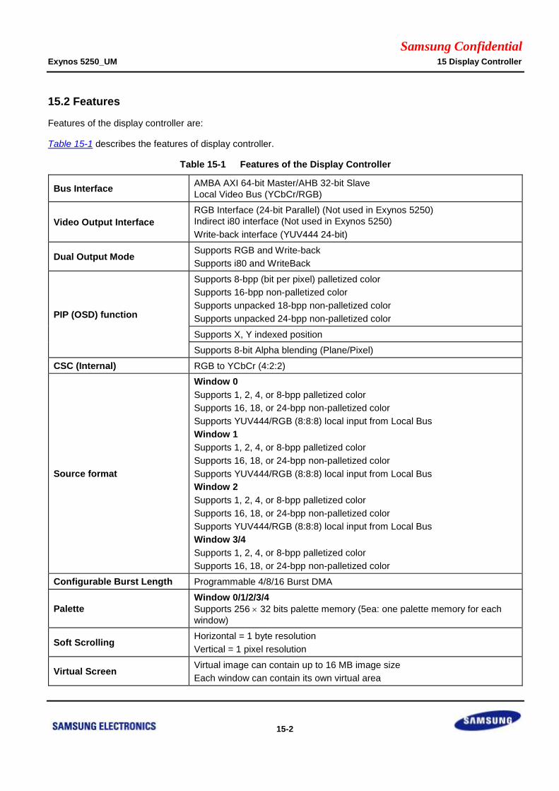
Samsung Confidential Exynos 5250_UM 15 Display Controller
15-2
15.2 Features
Features of the display controller are:
Table 15-1 describes the features of display controller.
Table 15-1 Features of the Display Controller
Bus Interface AMBA AXI 64-bit Master/AHB 32-bit Slave
Local Video Bus (YCbCr/RGB)
Video Output Interface
RGB Interface (24-bit Parallel) (Not used in Exynos 5250)
Indirect i80 interface (Not used in Exynos 5250)
Write-back interface (YUV444 24-bit)
Dual Output Mode Supports RGB and Write-back
Supports i80 and WriteBack
PIP (OSD) function
Supports 8-bpp (bit per pixel) palletized color
Supports 16-bpp non-palletized color
Supports unpacked 18-bpp non-palletized color
Supports unpacked 24-bpp non-palletized color
Supports X, Y indexed position
Supports 8-bit Alpha blending (Plane/Pixel)
CSC (Internal) RGB to YCbCr (4:2:2)
Source format
Window 0
Supports 1, 2, 4, or 8-bpp palletized color
Supports 16, 18, or 24-bpp non-palletized color
Supports YUV444/RGB (8:8:8) local input from Local Bus
Window 1
Supports 1, 2, 4, or 8-bpp palletized color
Supports 16, 18, or 24-bpp non-palletized color
Supports YUV444/RGB (8:8:8) local input from Local Bus
Window 2
Supports 1, 2, 4, or 8-bpp palletized color
Supports 16, 18, or 24-bpp non-palletized color
Supports YUV444/RGB (8:8:8) local input from Local Bus
Window 3/4
Supports 1, 2, 4, or 8-bpp palletized color
Supports 16, 18, or 24-bpp non-palletized color
Configurable Burst Length Programmable 4/8/16 Burst DMA
Palette
Window 0/1/2/3/4
Supports 256 32 bits palette memory (5ea: one palette memory for each
window)
Soft Scrolling Horizontal = 1 byte resolution
Vertical = 1 pixel resolution
Virtual Screen Virtual image can contain up to 16 MB image size
Each window can contain its own virtual area
Samsung Confidential Exynos 5250_UM 15 Display Controller
15-3
Transparent Overlay Supports Transparent Overlay
Color Key (Chroma Key) Supports Color Key function
Supports color key and blending function simultaneously
Image Enhancement Supports color gain control

Samsung Confidential Exynos 5250_UM 15 Display Controller
15-4
15.3 Functional Description of Display Controller
15.3.1 Sub-Block
The display controller consists of:
VSFR: To configure the display controller, the VSFR contains i80 command register set (12 registers) and five
256 32 palette memories.
VDMA: It is a dedicated display DMA that transfers video data in frame memory to VPRCS. By using this
DMA, you can display video data on screen without CPU intervention.
VPRCS: It receives video data from VDMA, converts the video data into a suitable data format, and sends it to
display link through RGB_VD. For example, the video data format is 8-bit per pixel mode (8-bpp mode) or 16-
bit per pixel mode (16-bpp mode).
VTIME: It consists of programmable logic to support the variable requirement of interface timing and rates that
is found in various LCD drivers. The VTIME block generates RGB_VSYNC, RGB_HSYNC, RGB_VCLK,
RGB_VDEN, VEN_VSYNC, VEN_HSYNC, VEN_FIELD, VEN_HREF and SYS_CS0, SYS_CS1, SYS_WE,
and so on.
Video clock generator
15.3.2 Data Flow
FIFO is located in the VDMA. When FIFO is empty or partially empty, the VDMA requests data from frame
memory based on the burst memory transfer mode. The data transfer rate determines the size of FIFO.
The display controller contains five FIFOs (three local FIFOs and two DMA FIFOs), to support the overlay window
display mode. You should use a FIFO for a screen display mode.
VPRCS obtains data from FIFO. It performs blending, image enhancing, scheduling, and overlay functions for final
image data. VPRCS can overlay up to five window images. It can blend a smaller or same sized window image
with the main window image that contains programmable alpha blending color (chroma) key function.
VDMA consists of:
Five DMA channels (Ch0 to Ch4)
Three local input interfaces
The Color Space Conversion (CSC) block converts Hue (YCbCr, local input only) data to RGB data to perform
blending. The alpha values written in SFR determine the level of blending. Data from output buffer appears in the
Video Data Port.
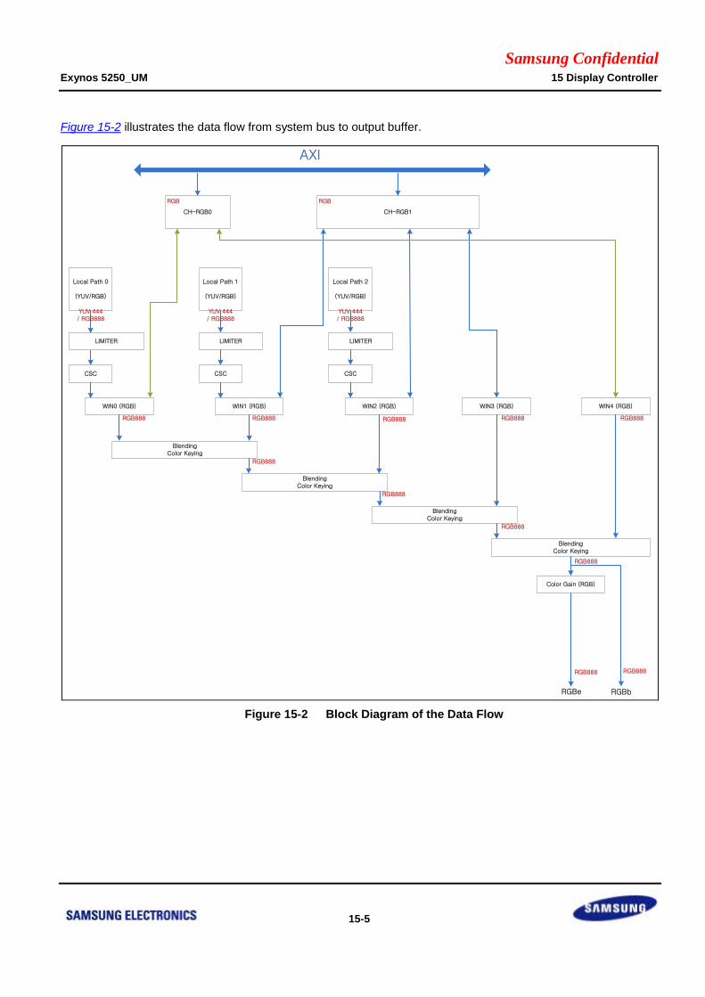
Samsung Confidential Exynos 5250_UM 15 Display Controller
15-5
Figure 15-2 illustrates the data flow from system bus to output buffer.
Local Path 0
(YUV/RGB)
Local Path 1
(YUV/RGB)
Local Path 2
(YUV/RGB)
LIMITER LIMITER LIMITER
CSC CSC CSC
WIN0 (RGB) WIN1 (RGB) WIN2 (RGB) WIN3 (RGB) WIN4 (RGB)
BlendingColor Keying
BlendingColor Keying
BlendingColor Keying
BlendingColor Keying
Color Gain (RGB)
AXI
RGBe
YUV 444/ RGB888
YUV 444/ RGB888
YUV 444/ RGB888
RGB888 RGB888 RGB888 RGB888 RGB888
RGB888
RGB888
RGB888
RGB888
RGB888
RGBb
RGB888
CH-RGB0 CH-RGB1
RGB RGB
Figure 15-2 Block Diagram of the Data Flow
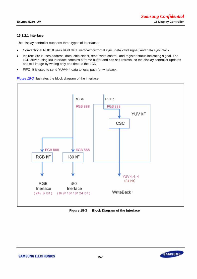
Samsung Confidential Exynos 5250_UM 15 Display Controller
15-6
15.3.2.1 Interface
The display controller supports three types of interfaces:
Conventional RGB: It uses RGB data, vertical/horizontal sync, data valid signal, and data sync clock.
Indirect i80: It uses address, data, chip select, read/ write control, and register/status indicating signal. The
LCD driver using i80 Interface contains a frame buffer and can self-refresh, so the display controller updates
one still image by writing only one time to the LCD
FIFO: It is used to send YUV444 data to local path for writeback.
Figure 15-3 illustrates the block diagram of the interface.
(24 bit)
Figure 15-3 Block Diagram of the Interface
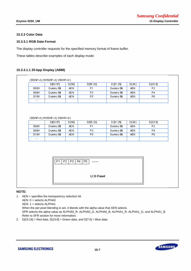
Samsung Confidential Exynos 5250_UM 15 Display Controller
15-7
15.3.3 Color Data
15.3.3.1 RGB Data Format
The display controller requests for the specified memory format of frame buffer.
These tables describe examples of each display mode:
15.3.3.1.1 25-bpp Display (A888)
NOTE:
1. AEN = specifies the transparency selection bit
AEN: 0 = selects ALPHA0
AEN: 1 = selects ALPHA1
When the per-pixel blending is set, it blends with the alpha value that AEN selects.
SFR selects the alpha value as ALPHA0_R, ALPHA0_G, ALPHA0_B, ALPHA1_R, ALPHA1_G, and ALPHA1_B.
Refer to SFR section for more information.
2. D[23:16] = Red data, D[15:8] = Green data, and D[7:0] = Blue data.

Samsung Confidential Exynos 5250_UM 15 Display Controller
15-8
15.3.3.1.2 32-bpp (8888) Mode
Pixel data contains alpha value.
000H
008H
010H
…
D[63:56] D[55:32]
ALPHA value P1
ALPHA value P3
ALPHA value P5
( BYSWP=0, HWSWP=0, WSWP=0 )
( BYSWP=0, HWSWP=0, WSWP=1 )
ALPHA value P2
ALPHA value P4
ALPHA value P6
D[31:24] D[23:0]
000H
008H
010H
…
ALPHA value P2
ALPHA value P4
ALPHA value P6
ALPHA value P1
ALPHA value P3
ALPHA value P5
D[63:56] D[55:32] D[31:24] D[23:0]
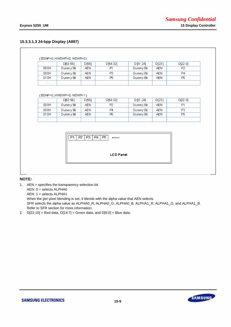
Samsung Confidential Exynos 5250_UM 15 Display Controller
15-9
15.3.3.1.3 24-bpp Display (A887)
NOTE:
1. AEN = specifies the transparency selection bit
AEN: 0 = selects ALPHA0
AEN: 1 = selects ALPHA1
When the per-pixel blending is set, it blends with the alpha value that AEN selects.
SFR selects the alpha value as ALPHA0_R, ALPHA0_G, ALPHA0_B, ALPHA1_R, ALPHA1_G, and ALPHA1_B.
Refer to SFR section for more information.
2. D[22:15] = Red data, D[14:7] = Green data, and D[6:0] = Blue data.
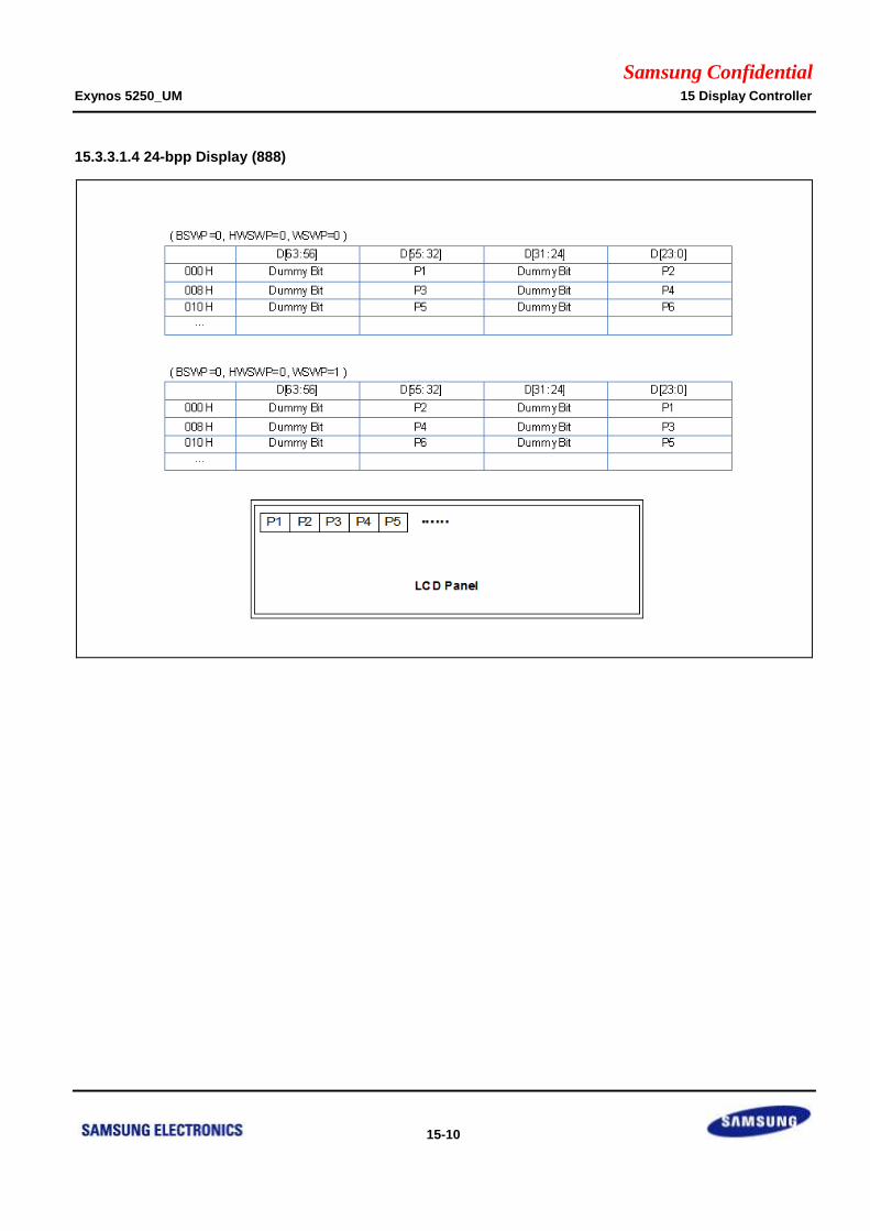
Samsung Confidential Exynos 5250_UM 15 Display Controller
15-10
15.3.3.1.4 24-bpp Display (888)
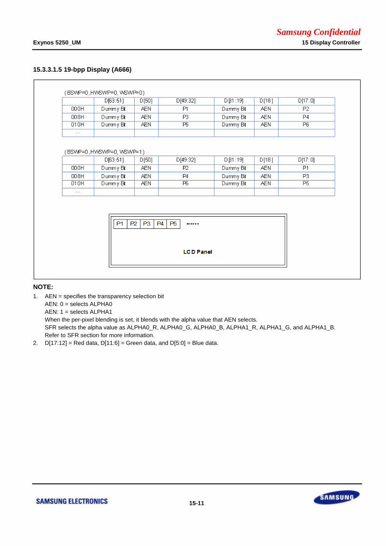
Samsung Confidential Exynos 5250_UM 15 Display Controller
15-11
15.3.3.1.5 19-bpp Display (A666)
NOTE:
1. AEN = specifies the transparency selection bit
AEN: 0 = selects ALPHA0
AEN: 1 = selects ALPHA1
When the per-pixel blending is set, it blends with the alpha value that AEN selects.
SFR selects the alpha value as ALPHA0_R, ALPHA0_G, ALPHA0_B, ALPHA1_R, ALPHA1_G, and ALPHA1_B.
Refer to SFR section for more information.
2. D[17:12] = Red data, D[11:6] = Green data, and D[5:0] = Blue data.
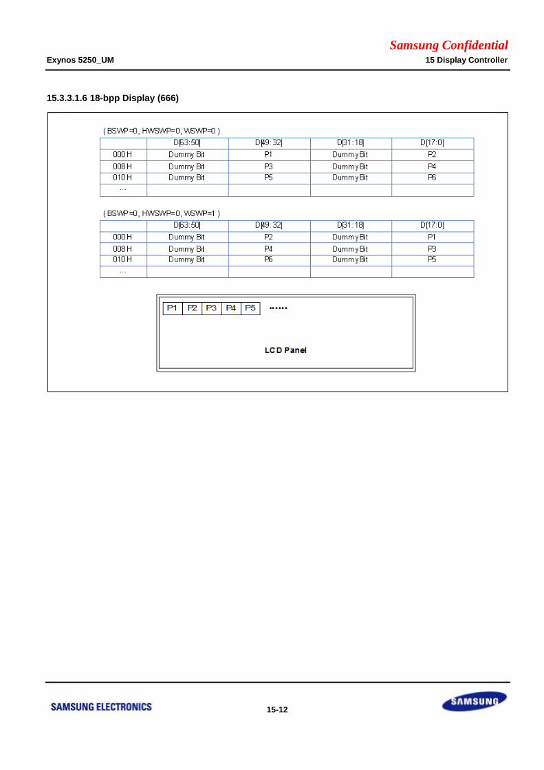
Samsung Confidential Exynos 5250_UM 15 Display Controller
15-12
15.3.3.1.6 18-bpp Display (666)
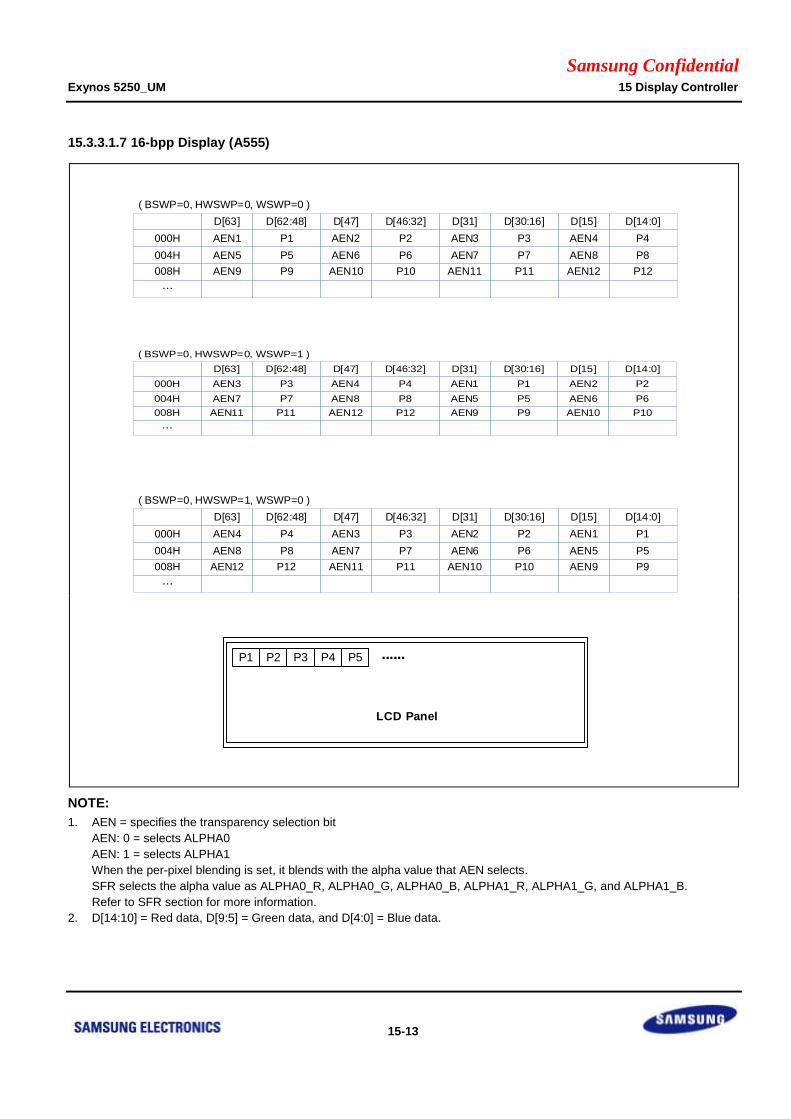
Samsung Confidential Exynos 5250_UM 15 Display Controller
15-13
15.3.3.1.7 16-bpp Display (A555)
NOTE:
1. AEN = specifies the transparency selection bit
AEN: 0 = selects ALPHA0
AEN: 1 = selects ALPHA1
When the per-pixel blending is set, it blends with the alpha value that AEN selects.
SFR selects the alpha value as ALPHA0_R, ALPHA0_G, ALPHA0_B, ALPHA1_R, ALPHA1_G, and ALPHA1_B.
Refer to SFR section for more information.
2. D[14:10] = Red data, D[9:5] = Green data, and D[4:0] = Blue data.
000H
004H
008H
…
D[62:48]
P1
P5
P9
( BSWP=0, HWSWP=0, WSWP=0 )
D[63]
AEN1
AEN5
AEN9
D[46:32]
P2
P6
P10
D[47]
AEN2
AEN6
AEN10
D[30:16]
P3
P7
P11
D[31]
AEN3
AEN7
AEN11
D[14:0]
P4
P8
P12
D[15]
AEN4
AEN8
AEN12
( BSWP=0, HWSWP=0, WSWP=1 )
000H
004H
008H
…
D[62:48]
P3
P7
P11
D[63]
AEN3
AEN7
AEN11
D[46:32]
P4
P8
P12
D[47]
AEN4
AEN8
AEN12
D[30:16]
P1
P5
P9
D[31]
AEN1
AEN5
AEN9
D[14:0]
P2
P6
P10
D[15]
AEN2
AEN6
AEN10
000H
004H
008H
…
D[62:48]
P4
P8
P12
D[63]
AEN4
AEN8
AEN12
D[46:32]
P3
P7
P11
D[47]
AEN3
AEN7
AEN11
D[30:16]
P2
P6
P10
D[31]
AEN2
AEN6
AEN10
D[14:0]
P1
P5
P9
D[15]
AEN1
AEN5
AEN9
( BSWP=0, HWSWP=1, WSWP=0 )
P1 P2 P3 P4 P5 ......
LCD Panel
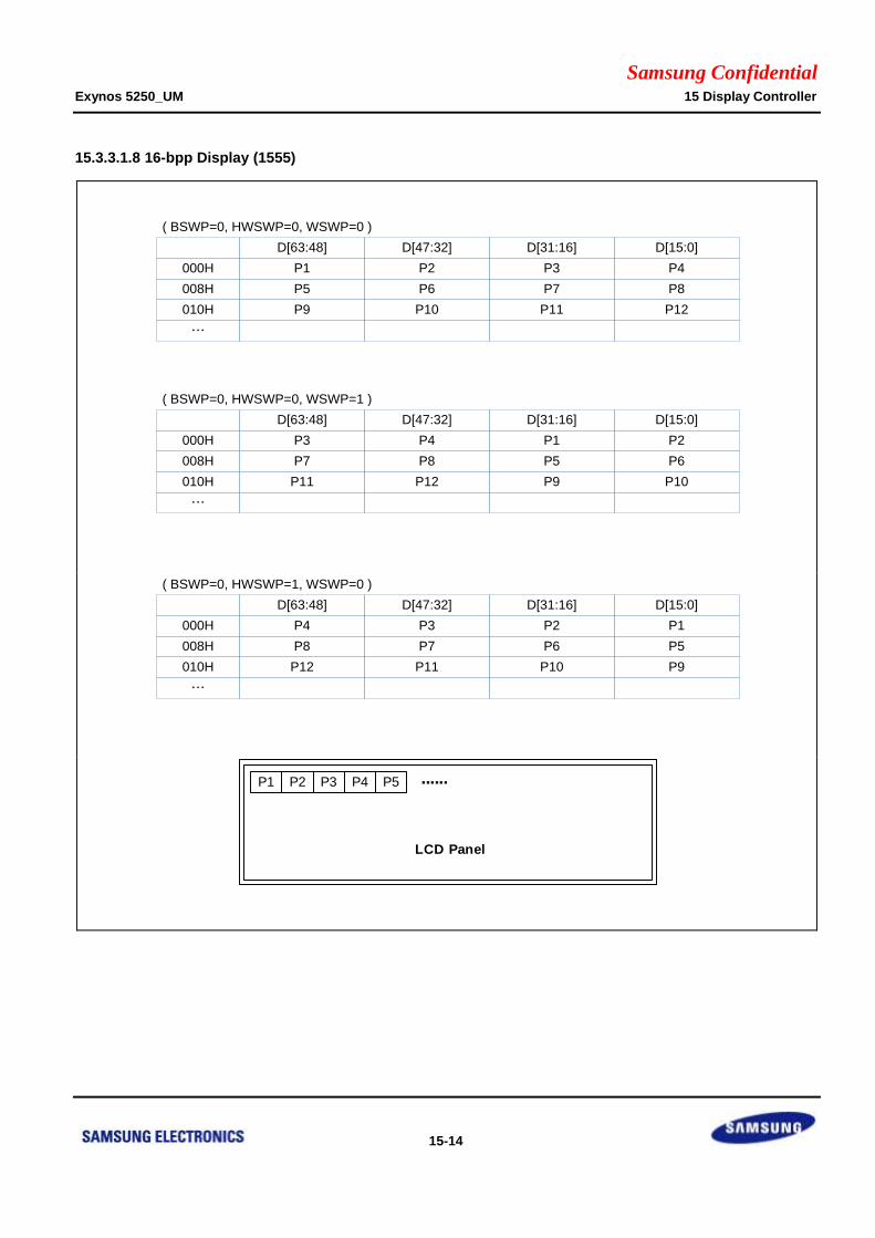
Samsung Confidential Exynos 5250_UM 15 Display Controller
15-14
15.3.3.1.8 16-bpp Display (1555)
( BSWP=0, HWSWP=0, WSWP=0 )
000H
008H
010H
…
D[63:48] D[47:32]
P1 P2
P6
P10
P5
P9
D[31:16] D[15:0]
P3 P4
P8
P12
P7
P11
( BSWP=0, HWSWP=0, WSWP=1 )
000H
008H
010H
…
D[63:48] D[47:32]
P3 P4
P8
P12
P7
P11
D[31:16] D[15:0]
P1 P2
P6
P10
P5
P9
( BSWP=0, HWSWP=1, WSWP=0 )
000H
008H
010H
…
D[63:48] D[47:32]
P1P2
P6
P10
P5
P9
D[31:16] D[15:0]
P3P4
P8
P12
P7
P11
P1 P2 P3 P4 P5 ......
LCD Panel
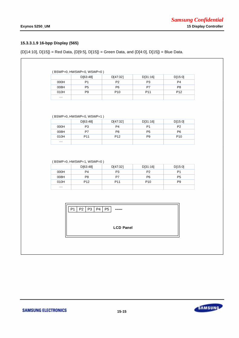
Samsung Confidential Exynos 5250_UM 15 Display Controller
15-15
15.3.3.1.9 16-bpp Display (565)
{D[14:10], D[15]} = Red Data, {D[9:5], D[15]} = Green Data, and {D[4:0], D[15]} = Blue Data.
( BSWP=0, HWSWP=0, WSWP=0 )
000H
008H
010H
…
D[63:48] D[47:32]
P1 P2
P6
P10
P5
P9
D[31:16] D[15:0]
P3 P4
P8
P12
P7
P11
( BSWP=0, HWSWP=0, WSWP=1 )
000H
008H
010H
…
D[63:48] D[47:32]
P3 P4
P8
P12
P7
P11
D[31:16] D[15:0]
P1 P2
P6
P10
P5
P9
( BSWP=0, HWSWP=1, WSWP=0 )
000H
008H
010H
…
D[63:48] D[47:32]
P1P2
P6
P10
P5
P9
D[31:16] D[15:0]
P3P4
P8
P12
P7
P11
P1 P2 P3 P4 P5 ......
LCD Panel
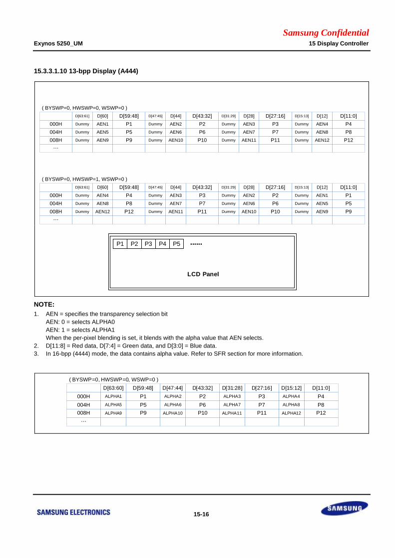
Samsung Confidential Exynos 5250_UM 15 Display Controller
15-16
15.3.3.1.10 13-bpp Display (A444)
NOTE:
1. AEN = specifies the transparency selection bit
AEN: 0 = selects ALPHA0
AEN: 1 = selects ALPHA1
When the per-pixel blending is set, it blends with the alpha value that AEN selects.
2. D[11:8] = Red data, D[7:4] = Green data, and D[3:0] = Blue data.
3. In 16-bpp (4444) mode, the data contains alpha value. Refer to SFR section for more information.
000H
004H
008H
…
D[59:48]
P1
P5
P9
( BYSWP=0, HWSWP=0, WSWP=0 )
D[60]
AEN1
AEN5
AEN9
D[43:32]
P2
P6
P10
D[44]
AEN2
AEN6
AEN10
D[27:16]
P3
P7
P11
D[28]
AEN3
AEN7
AEN11
D[11:0]
P4
P8
P12
D[12]
AEN4
AEN8
AEN12
D[63:61]
Dummy
Dummy
Dummy
D[47:45]
Dummy
Dummy
Dummy
D[31:29]
Dummy
Dummy
Dummy
D[15:13]
Dummy
Dummy
Dummy
( BYSWP=0, HWSWP=1, WSWP=0 )
000H
004H
008H
…
P1
P5
P9
AEN1
AEN5
AEN9
P2
P6
P10
AEN2
AEN6
AEN10
P3
P7
P11
AEN3
AEN7
AEN11
P4
P8
P12
AEN4
AEN8
AEN12
Dummy
Dummy
Dummy
Dummy
Dummy
Dummy
Dummy
Dummy
Dummy
Dummy
Dummy
Dummy
D[59:48]D[60] D[43:32]D[44] D[27:16]D[28] D[11:0]D[12]D[63:61] D[47:45] D[31:29] D[15:13]
P1 P2 P3 P4 P5 ......
LCD Panel
( BYSWP=0, HWSWP=0, WSWP=0 )
000H
004H
008H
…
D[59:48]
P1
P5
P9
D[63:60]
ALPHA1
ALPHA5
ALPHA9
D[43:32]
P2
P6
P10
D[47:44]
ALPHA2
ALPHA6
ALPHA10
D[27:16]
P3
P7
P11
D[31:28]
ALPHA3
ALPHA7
ALPHA11
D[11:0]
P4
P8
P12
D[15:12]
ALPHA4
ALPHA8
ALPHA12
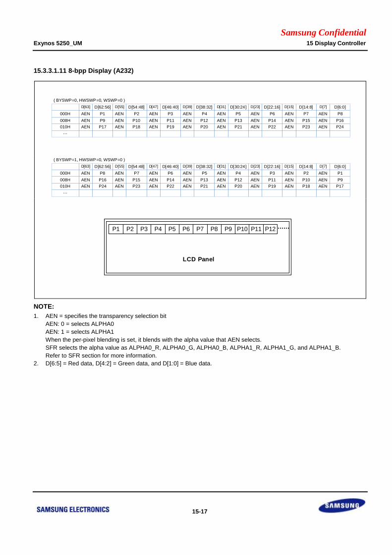
Samsung Confidential Exynos 5250_UM 15 Display Controller
15-17
15.3.3.1.11 8-bpp Display (A232)
NOTE:
1. AEN = specifies the transparency selection bit
AEN: 0 = selects ALPHA0
AEN: 1 = selects ALPHA1
When the per-pixel blending is set, it blends with the alpha value that AEN selects.
SFR selects the alpha value as ALPHA0_R, ALPHA0_G, ALPHA0_B, ALPHA1_R, ALPHA1_G, and ALPHA1_B.
Refer to SFR section for more information.
2. D[6:5] = Red data, D[4:2] = Green data, and D[1:0] = Blue data.
( BYSWP=0, HWSWP=0, WSWP=0 )
000H
008H
010H
…
D[63]
AEN
AEN
AEN
D[62:56]
P1
P9
P17
D[55]
AEN
AEN
AEN
D[54:48]
P2
P10
P18
D[47]
AEN
AEN
AEN
D[46:40]
P3
P11
P19
D[39]
AEN
AEN
AEN
D[38:32]
P4
P12
P20
D[31]
AEN
AEN
AEN
D[30:24]
P5
P13
P21
D[23]
AEN
AEN
AEN
D[22:16]
P6
P14
P22
D[15]
AEN
AEN
AEN
D[14:8]
P7
P15
P23
D[7]
AEN
AEN
AEN
D[6:0]
P8
P16
P24
( BYSWP=1, HWSWP=0, WSWP=0 )
000H
008H
010H
…
D[63]
AEN
AEN
AEN
D[62:56]
P1
P9
P17
D[55]
AEN
AEN
AEN
D[54:48]
P2
P10
P18
D[47]
AEN
AEN
AEN
D[46:40]
P3
P11
P19
D[39]
AEN
AEN
AEN
D[38:32]
P4
P12
P20
D[31]
AEN
AEN
AEN
D[30:24]
P5
P13
P21
D[23]
AEN
AEN
AEN
D[22:16]
P6
P14
P22
D[15]
AEN
AEN
AEN
D[14:8]
P7
P15
P23
D[7]
AEN
AEN
AEN
D[6:0]
P8
P16
P24
P1 P2 P3 P4 P5 ......
LCD Panel
P6 P7 P8 P10 P11 P12P9
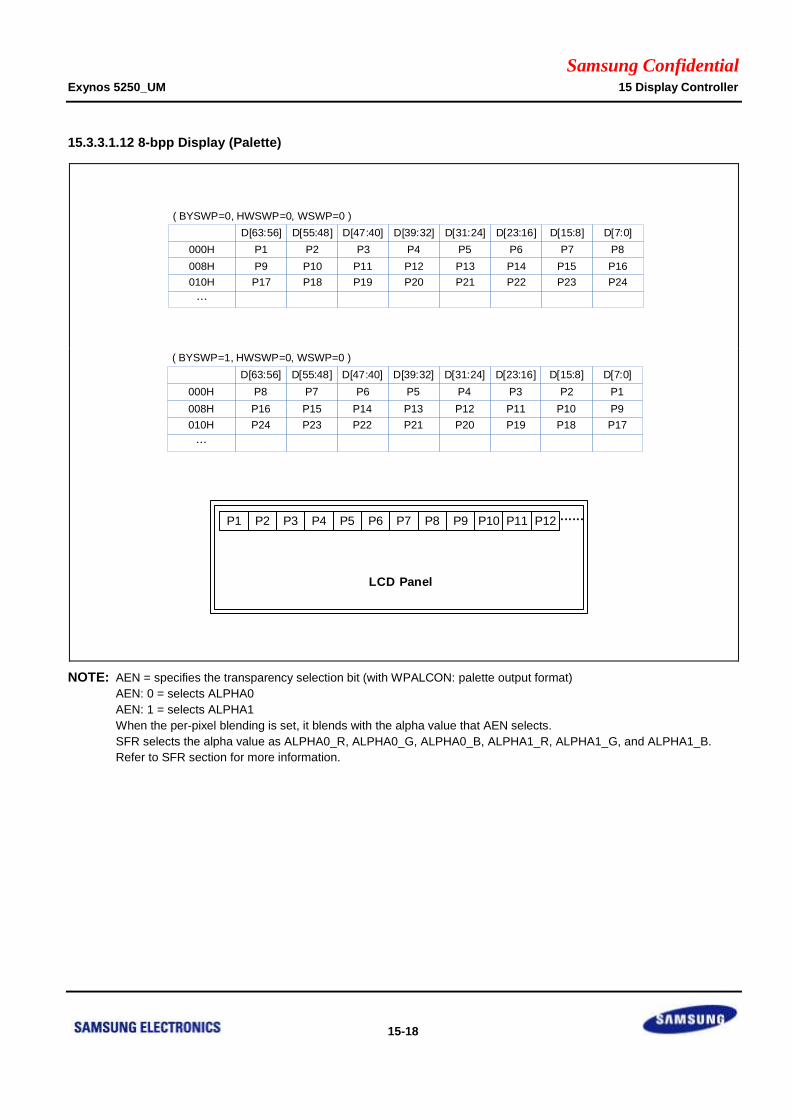
Samsung Confidential Exynos 5250_UM 15 Display Controller
15-18
15.3.3.1.12 8-bpp Display (Palette)
NOTE: AEN = specifies the transparency selection bit (with WPALCON: palette output format)
AEN: 0 = selects ALPHA0
AEN: 1 = selects ALPHA1
When the per-pixel blending is set, it blends with the alpha value that AEN selects.
SFR selects the alpha value as ALPHA0_R, ALPHA0_G, ALPHA0_B, ALPHA1_R, ALPHA1_G, and ALPHA1_B.
Refer to SFR section for more information.
( BYSWP=0, HWSWP=0, WSWP=0 )
000H
008H
010H
…
D[63:56]
P1
P9
P17
D[55:48]
P2
P10
P18
D[47:40]
P3
P11
P19
D[39:32]
P4
P12
P20
D[31:24]
P5
P13
P21
D[23:16]
P6
P14
P22
D[15:8]
P7
P15
P23
D[7:0]
P8
P16
P24
( BYSWP=1, HWSWP=0, WSWP=0 )
000H
008H
010H
…
P1
P9
P17
P2
P10
P18
P3
P11
P19
P4
P12
P20
P5
P13
P21
P6
P14
P22
P7
P15
P23
P8
P16
P24
D[63:56] D[55:48] D[47:40] D[39:32] D[31:24] D[23:16] D[15:8] D[7:0]
P1 P2 P3 P4 P5 ......
LCD Panel
P6 P7 P8 P10 P11 P12P9
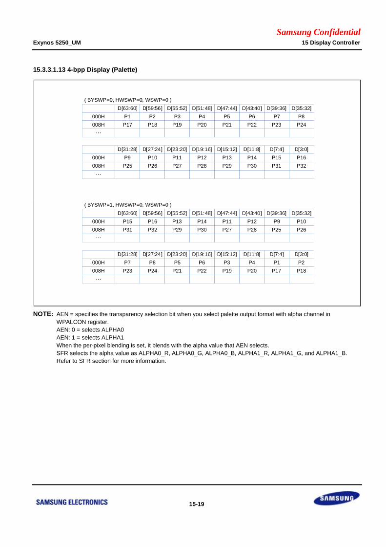
Samsung Confidential Exynos 5250_UM 15 Display Controller
15-19
15.3.3.1.13 4-bpp Display (Palette)
NOTE: AEN = specifies the transparency selection bit when you select palette output format with alpha channel in
WPALCON register.
AEN: 0 = selects ALPHA0
AEN: 1 = selects ALPHA1
When the per-pixel blending is set, it blends with the alpha value that AEN selects.
SFR selects the alpha value as ALPHA0_R, ALPHA0_G, ALPHA0_B, ALPHA1_R, ALPHA1_G, and ALPHA1_B.
Refer to SFR section for more information.
( BYSWP=0, HWSWP=0, WSWP=0 )
000H
008H
…
D[63:60]
P1
P17
D[59:56]
P2
P18
D[55:52]
P3
P19
D[51:48]
P4
P20
D[47:44]
P5
P21
D[43:40]
P6
P22
D[39:36]
P7
P23
D[35:32]
P8
P24
D[31:28]
P25
D[27:24]
P26
D[23:20]
P27
D[19:16]
P28
D[15:12]
P29
D[11:8]
P30
D[7:4]
P31
D[3:0]
P32
000H
008H
…
P9 P10 P11 P12 P13 P14 P15 P16
( BYSWP=1, HWSWP=0, WSWP=0 )
000H
008H
…
D[63:60]
P1
P17
D[59:56]
P2
P18
D[55:52]
P3
P19
D[51:48]
P4
P20
D[47:44]
P5
P21
D[43:40]
P6
P22
D[39:36]
P7
P23
D[35:32]
P8
P24
D[31:28]
P25
D[27:24]
P26
D[23:20]
P27
D[19:16]
P28
D[15:12]
P29
D[11:8]
P30
D[7:4]
P31
D[3:0]
P32
000H
008H
…
P9 P10P11 P12P13 P14P15 P16
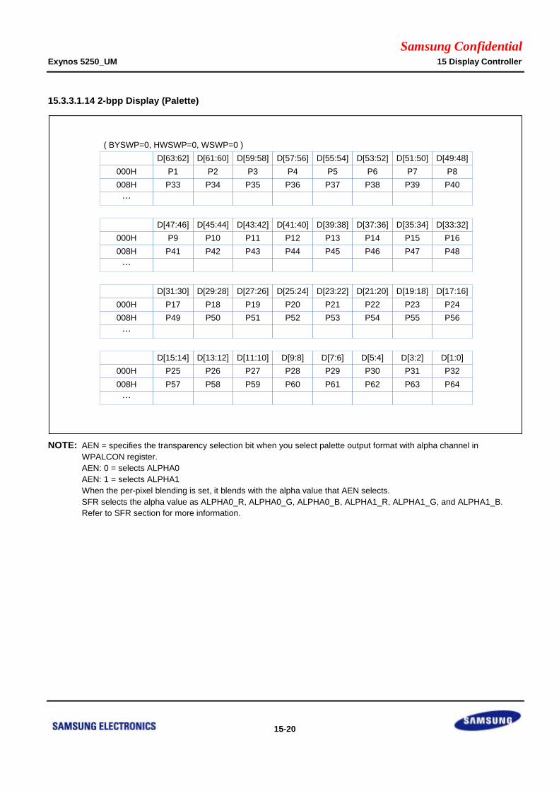
Samsung Confidential Exynos 5250_UM 15 Display Controller
15-20
15.3.3.1.14 2-bpp Display (Palette)
NOTE: AEN = specifies the transparency selection bit when you select palette output format with alpha channel in
WPALCON register.
AEN: 0 = selects ALPHA0
AEN: 1 = selects ALPHA1
When the per-pixel blending is set, it blends with the alpha value that AEN selects.
SFR selects the alpha value as ALPHA0_R, ALPHA0_G, ALPHA0_B, ALPHA1_R, ALPHA1_G, and ALPHA1_B.
Refer to SFR section for more information.
( BYSWP=0, HWSWP=0, WSWP=0 )
000H
008H
…
D[63:62]
P1
P33
D[61:60]
P2
P34
D[59:58]
P3
P35
D[57:56]
P4
P36
D[55:54]
P5
P37
D[53:52]
P6
P38
D[51:50]
P7
P39
D[49:48]
P8
P40
D[47:46]
P41
D[45:44]
P42
D[43:42]
P43
D[41:40]
P44
D[39:38]
P45
D[37:36]
P46
D[35:34]
P47
D[33:32]
P48
000H
008H
…
P9 P10 P11 P12 P13 P14 P15 P16
D[31:30] D[29:28] D[27:26] D[25:24] D[23:22] D[21:20] D[19:18] D[17:16]
000H
008H
…
D[15:14] D[13:12] D[11:10] D[9:8] D[7:6] D[5:4] D[3:2] D[1:0]
000H
008H
…
P17
P49
P18
P50
P19
P51
P20
P52
P21
P53
P22
P54
P23
P55
P24
P56
P25
P57
P26
P58
P27
P59
P28
P60
P29
P61
P30
P62
P31
P63
P32
P64
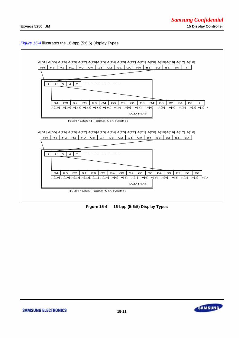
Samsung Confidential Exynos 5250_UM 15 Display Controller
15-21
Figure 15-4 illustrates the 16-bpp (5:6:5) Display Types
Figure 15-4 16-bpp (5:6:5) Display Types
1 2 3 4 5
LCD Panel
16BPP 5:5:5+1 Format(Non-Palette)
A[31] A[30] A[29] A[28] A[27] A[26]A[25] A[24] A[23] A[22] A[21] A[20] A[19]A[18] A[17] A[16]
R4 R3 R2 R1 R0 G4 G3 G2 G1 G0 R4 B3 B2 B1 B0 I
A[15] A[14] A[13] A[12] A[11] A[10] A[9] A[8] A[7] A[6] A[5] A[4] A[3] A[2] A[1] A[0]
R4 R3 R2 R1 R0 G4 G3 G2 G1 G0 R4 B3 B2 B1 B0 I
1 2 3 4 5
LCD Panel
16BPP 5:6:5 Format(Non-Palette)
A[31] A[30] A[29] A[28] A[27] A[26]A[25] A[24] A[23] A[22] A[21] A[20] A[19]A[18] A[17] A[16]
A[15] A[14] A[13] A[12]A[11] A[10] A[9] A[8] A[7] A[6] A[5] A[4] A[3] A[2] A[1] A[0]
R4 R3 R2 R1 R0 G5 G4 G3 G2 G1 G0 B4 B3 B2 B1 B0
R4 R3 R2 R1 R0 G5 G4 G3 G2 G1 G0 B4 B3 B2 B1 B0
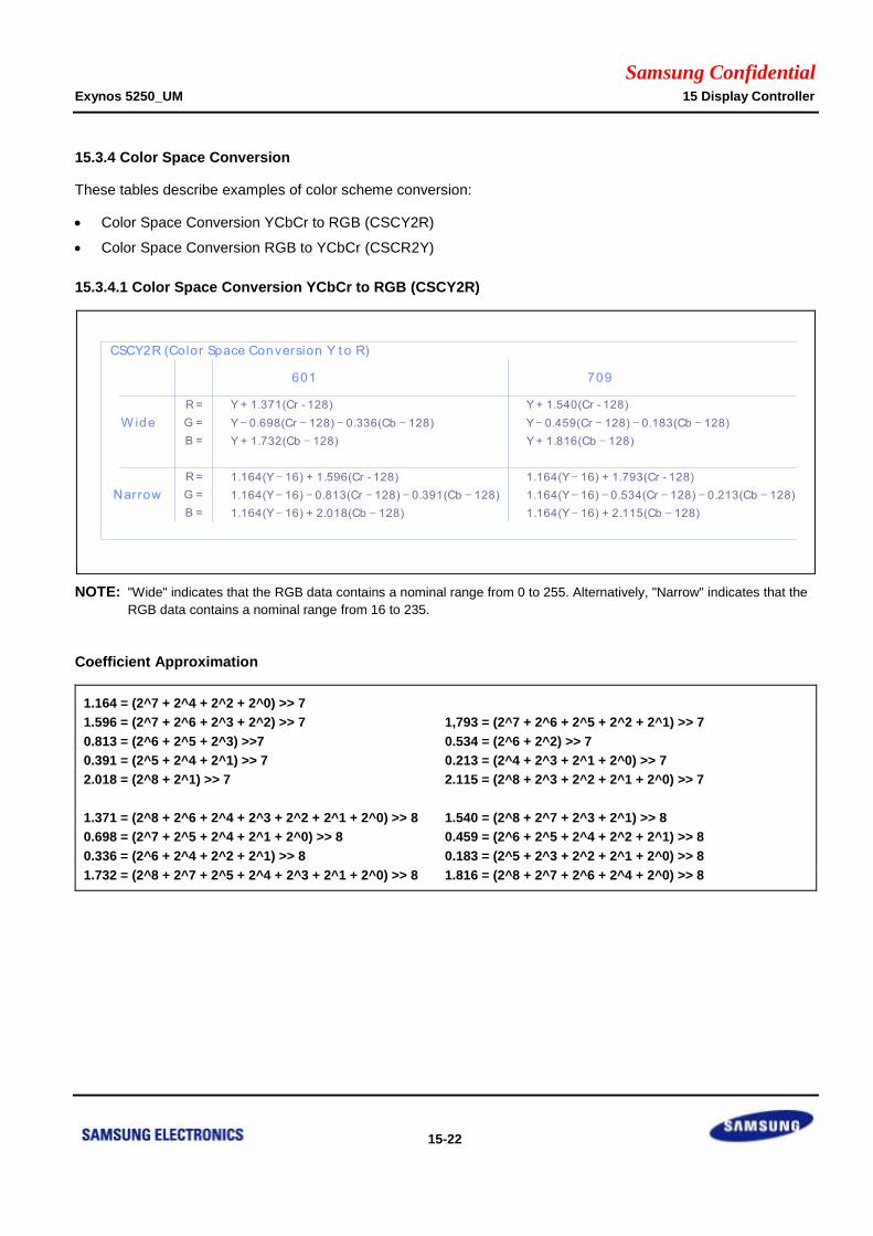
Samsung Confidential Exynos 5250_UM 15 Display Controller
15-22
15.3.4 Color Space Conversion
These tables describe examples of color scheme conversion:
Color Space Conversion YCbCr to RGB (CSCY2R)
Color Space Conversion RGB to YCbCr (CSCR2Y)
15.3.4.1 Color Space Conversion YCbCr to RGB (CSCY2R)
NOTE: "Wide" indicates that the RGB data contains a nominal range from 0 to 255. Alternatively, "Narrow" indicates that the
RGB data contains a nominal range from 16 to 235.
Coefficient Approximation
1.164 = (2^7 + 2^4 + 2^2 + 2^0) >> 7
1.596 = (2^7 + 2^6 + 2^3 + 2^2) >> 7 1,793 = (2^7 + 2^6 + 2^5 + 2^2 + 2^1) >> 7
0.813 = (2^6 + 2^5 + 2^3) >>7 0.534 = (2^6 + 2^2) >> 7
0.391 = (2^5 + 2^4 + 2^1) >> 7 0.213 = (2^4 + 2^3 + 2^1 + 2^0) >> 7
2.018 = (2^8 + 2^1) >> 7 2.115 = (2^8 + 2^3 + 2^2 + 2^1 + 2^0) >> 7
1.371 = (2^8 + 2^6 + 2^4 + 2^3 + 2^2 + 2^1 + 2^0) >> 8 1.540 = (2^8 + 2^7 + 2^3 + 2^1) >> 8
0.698 = (2^7 + 2^5 + 2^4 + 2^1 + 2^0) >> 8 0.459 = (2^6 + 2^5 + 2^4 + 2^2 + 2^1) >> 8
0.336 = (2^6 + 2^4 + 2^2 + 2^1) >> 8 0.183 = (2^5 + 2^3 + 2^2 + 2^1 + 2^0) >> 8
1.732 = (2^8 + 2^7 + 2^5 + 2^4 + 2^3 + 2^1 + 2^0) >> 8 1.816 = (2^8 + 2^7 + 2^6 + 2^4 + 2^0) >> 8
CSCY2R (Color Space Conversion Y t o R)
R = Y + 1.371(Cr - 128)
G =
B =
Y – 0.698(Cr – 128) – 0.336(Cb – 128)
Y + 1.732(Cb – 128)
R =
G =
B =
601 709
Narrow
W ide
1.164(Y – 16) + 1.596(Cr - 128)
1.164(Y – 16) – 0.813(Cr – 128) – 0.391(Cb – 128)
1.164(Y – 16) + 2.018(Cb – 128)
Y + 1.540(Cr - 128)
Y – 0.459(Cr – 128) – 0.183(Cb – 128)
Y + 1.816(Cb – 128)
1.164(Y – 16) + 1.793(Cr - 128)
1.164(Y – 16) – 0.534(Cr – 128) – 0.213(Cb – 128)
1.164(Y – 16) + 2.115(Cb – 128)
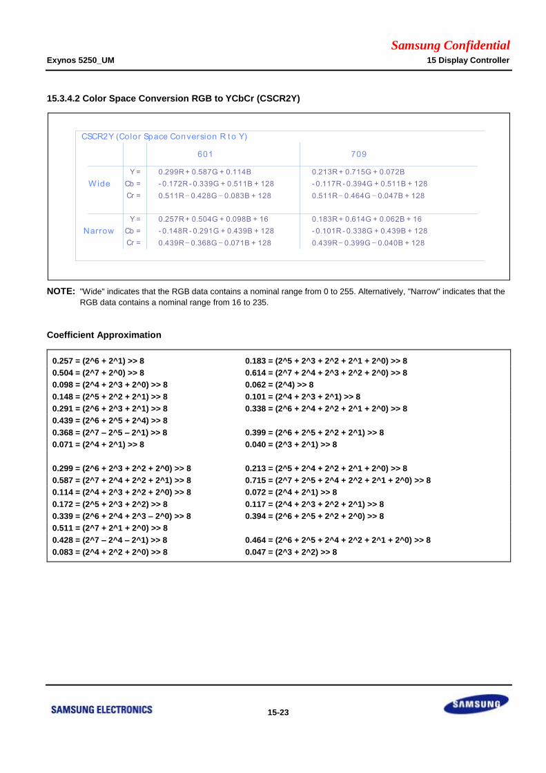
Samsung Confidential Exynos 5250_UM 15 Display Controller
15-23
15.3.4.2 Color Space Conversion RGB to YCbCr (CSCR2Y)
NOTE: "Wide" indicates that the RGB data contains a nominal range from 0 to 255. Alternatively, "Narrow" indicates that the
RGB data contains a nominal range from 16 to 235.
Coefficient Approximation
0.257 = (2^6 + 2^1) >> 8 0.183 = (2^5 + 2^3 + 2^2 + 2^1 + 2^0) >> 8
0.504 = (2^7 + 2^0) >> 8 0.614 = (2^7 + 2^4 + 2^3 + 2^2 + 2^0) >> 8
0.098 = (2^4 + 2^3 + 2^0) >> 8 0.062 = (2^4) >> 8
0.148 = (2^5 + 2^2 + 2^1) >> 8 0.101 = (2^4 + 2^3 + 2^1) >> 8
0.291 = (2^6 + 2^3 + 2^1) >> 8 0.338 = (2^6 + 2^4 + 2^2 + 2^1 + 2^0) >> 8
0.439 = (2^6 + 2^5 + 2^4) >> 8
0.368 = (2^7 – 2^5 – 2^1) >> 8 0.399 = (2^6 + 2^5 + 2^2 + 2^1) >> 8
0.071 = (2^4 + 2^1) >> 8 0.040 = (2^3 + 2^1) >> 8
0.299 = (2^6 + 2^3 + 2^2 + 2^0) >> 8 0.213 = (2^5 + 2^4 + 2^2 + 2^1 + 2^0) >> 8
0.587 = (2^7 + 2^4 + 2^2 + 2^1) >> 8 0.715 = (2^7 + 2^5 + 2^4 + 2^2 + 2^1 + 2^0) >> 8
0.114 = (2^4 + 2^3 + 2^2 + 2^0) >> 8 0.072 = (2^4 + 2^1) >> 8
0.172 = (2^5 + 2^3 + 2^2) >> 8 0.117 = (2^4 + 2^3 + 2^2 + 2^1) >> 8
0.339 = (2^6 + 2^4 + 2^3 – 2^0) >> 8 0.394 = (2^6 + 2^5 + 2^2 + 2^0) >> 8
0.511 = (2^7 + 2^1 + 2^0) >> 8
0.428 = (2^7 – 2^4 – 2^1) >> 8 0.464 = (2^6 + 2^5 + 2^4 + 2^2 + 2^1 + 2^0) >> 8
0.083 = (2^4 + 2^2 + 2^0) >> 8 0.047 = (2^3 + 2^2) >> 8
CSCR2Y (Color Space Conversion R t o Y)
Y = 0.299R + 0.587G + 0.114B
Cb =
Cr =
- 0.172R - 0.339G + 0.511B + 128
0.511R – 0.428G – 0.083B + 128
0.213R + 0.715G + 0.072B
- 0.117R - 0.394G + 0.511B + 128
0.511R – 0.464G – 0.047B + 128
Y = 0.257R + 0.504G + 0.098B + 16
Cb =
Cr =
- 0.148R - 0.291G + 0.439B + 128
0.439R – 0.368G – 0.071B + 128
601 709
Narrow
W ide
0.183R + 0.614G + 0.062B + 16
- 0.101R - 0.338G + 0.439B + 128
0.439R – 0.399G – 0.040B + 128

Samsung Confidential Exynos 5250_UM 15 Display Controller
15-24
15.3.5 Palette Usage
15.3.5.1 Palette Configuration and Format Control
The display controller supports 256-color palette to select color mapping. You can select up to 256 colors from 32-
bit colors by using below formats.
A 256-color palette consists of 256 (depth) 32-bit SPSRAM. It supports 8:8:8, 6:6:6, 5:6:5 (R: G: B), and other
formats.
For Example:
Refer to A:5:5:5 format, Write palette, as described in Table 15-2.
Connect VD pin to TFT LCD panel (R(5) = VD[23:19], G(5) = VD[15:11], and B (5) = VD[7:3]). AEN bit enables or
disables the blending function. Finally, set WPALCON (W1PAL, case window0) register to 0’b101. The 32-bit
(8:8:8:8) format contains an alpha value directly, without using the alpha value register (ALPHA_0/1).
Table 15-2 describes the 32-bpp (8:8:8:8) palette data format.
Table 15-2 32-bpp (8:8:8:8) Palette Data Format
Table 15-3 describes the 25-bpp (A: 8:8:8) palette data format.
Table 15-3 25-bpp (A: 8:8:8) Palette Data Format
INDEX /Bit Pos.
31
30
29
28
27
26
25
24
23
22
21
20
19
18
17
16
15
14
13
12
11
10
9 8 7 6 5 4 3 2 1 0
00h
01h
……
FFh
Numberof VD
ALPHA
ALPHA
ALPHA
……………… ………………………………………… …………………………
R
7
R
6
R
5
R
4
R
3
R
2
R
1
R
0
R7
R6
R5
R4
R3
R2
R1
R0
R7
R6
R5
R4
R3
R2
R1
R0
- - - -- -- -23
22
21
20
19
18
17
16
15
14
13
12
11
10
9 8 7 6 5 4 3 2 1 0
G
7
G
6
G
5
G
4
G
3
G
2
G
1
G
0
G7
G6
G5
G4
G3
G2
G1
G0
G7
G6
G5
G4
G3
G2
G1
G0
B
7
B
6
B
5
B
4
B
3
B
2
B
1
B
0
B7
B6
B5
B4
B3
B2
B1
B0
B7
B6
B5
B4
B3
B2
B1
B0
INDEX /
Bit Pos.
3
1
3
0
2
9
2
8
2
7
2
6
2
5
2
4
2
3
2
2
2
1
2
0
1
9
1
8
1
7
1
6
1
5
1
4
1
3
1
2
1
1
1
09 8 7 6 5 4 3 2 1 0
00h
01h
……
FFh
Numberof VD
……………………………………………………………………………………
R
7
R
6
R
5
R
4
R
3
R
2
R
1
R
0
R7
R6
R5
R4
R3
R2
R1
R0
R7
R6
R5
R4
R3
R2
R1
R0
- - - -- -- -23
22
21
20
19
18
17
16
15
14
13
12
11
10
9 8 7 6 5 4 3 2 1 0
G
7
G
6
G
5
G
4
G
3
G
2
G
1
G
0
G7
G6
G5
G4
G3
G2
G1
G0
G7
G6
G5
G4
G3
G2
G1
G0
B
7
B
6
B
5
B
4
B
3
B
2
B
1
B
0
B7
B6
B5
B4
B3
B2
B1
B0
B7
B6
B5
B4
B3
B2
B1
B0
- - -A
E
N- -- -
- - -AE
N- -- -
- - -A
EN
- -- -
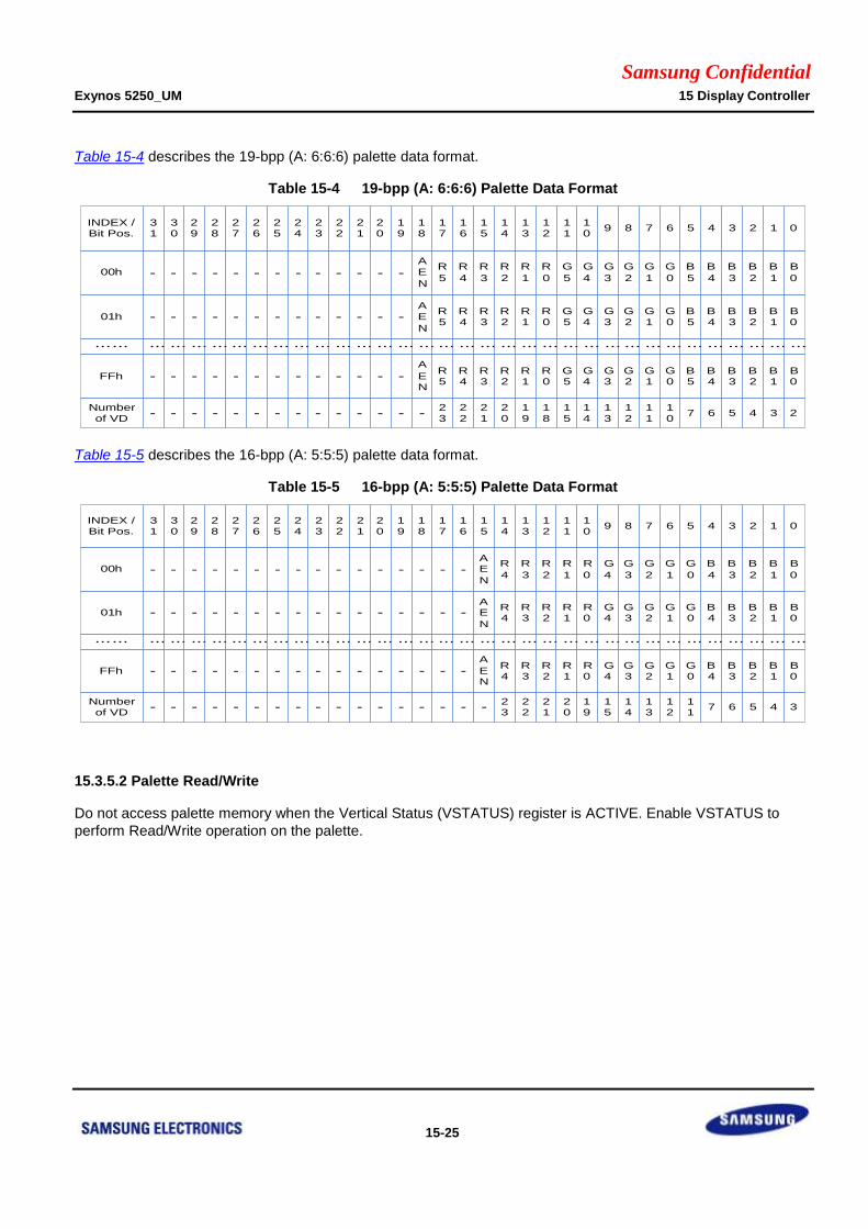
Samsung Confidential Exynos 5250_UM 15 Display Controller
15-25
Table 15-4 describes the 19-bpp (A: 6:6:6) palette data format.
Table 15-4 19-bpp (A: 6:6:6) Palette Data Format
Table 15-5 describes the 16-bpp (A: 5:5:5) palette data format.
Table 15-5 16-bpp (A: 5:5:5) Palette Data Format
15.3.5.2 Palette Read/Write
Do not access palette memory when the Vertical Status (VSTATUS) register is ACTIVE. Enable VSTATUS to
perform Read/Write operation on the palette.
INDEX /Bit Pos.
31
30
29
28
27
26
25
24
23
22
21
20
19
18
17
16
15
14
13
12
11
10
9 8 7 6 5 4 3 2 1 0
00h
01h
……
FFh
Numberof VD
……………………………………………………………………………………
R
5
R
4
R
3
R
2
R
1
R
0
- - - -- -- -23
22
21
20
19
18
15
14
13
12
11
10
7 6 5 4 3 2
G
5
G
4
G
3
G
2
G
1
G
0
B
5
B
4
B
3
B
2
B
1
B
0- - -AE
N- -- -
- - -- -- -
- - -- -- -
- -- -- -
- -- -- -
R5
R4
R3
R2
R1
R0
G5
G4
G3
G2
G1
G0
B5
B4
B3
B2
B1
B0
AE
N- -- -- -
R5
R4
R3
R2
R1
R0
G5
G4
G3
G2
G1
G0
B5
B4
B3
B2
B1
B0
A
EN
- -- -- -
INDEX /Bit Pos.
31
30
29
28
27
26
25
24
23
22
21
20
19
18
17
16
15
14
13
12
11
10
9 8 7 6 5 4 3 2 1 0
00h
01h
……
FFh
Numberof VD
…… ………… …… …… …… ………… …… …… …… …… ……… …… …… …
R
4
R
3
R
2
R
1
R
0
- - - -- -- -23
22
21
20
19
15
14
13
12
11
7 6 5 4 3
G
4
G
3
G
2
G
1
G
0
B
4
B
3
B
2
B
1
B
0- - -
AE
N- -- -
- - -- -- -
- - -- -- -
- -- -- -
- -- -- -
- -- -- -
- -- -- -
- --
---
R4
R3
R2
R1
R0
G4
G3
G2
G1
G0
B4
B3
B2
B1
B0
AE
N---
R4
R3
R2
R1
R0
G4
G3
G2
G1
G0
B4
B3
B2
B1
B0
A
EN
---
Samsung Confidential Exynos 5250_UM 15 Display Controller
15-26
15.3.6 Window Blending
15.3.6.1 Overview
The main function of the VPRCS module is window blending. The display controller consists of five window layers
(win0 to win4).
Example of Application:
The system uses:
win0 as OS window, full TV screen window, and so on
win1 as small (next channel ) TV screen with win2 as menu
win3 as caption
win4 as channel information
win3 and win4 have color limitation when it uses color index with Color LUT. This feature reduces the data rate of total
system. Thus, it enhances the system performance.
Example of Total Five Windows:
win0 (base): Local/ (YCbCr, RGB without palette)
win1 (Overlay1): RGB with palette
win2 (Overlay2): RGB with palette
win3 (Caption): RGB (1/2/4) with 16-level Color LUT
win4 (Cursor): RGB (1/2) with 4-level Color LUT
Overlay Priority
win4 > win3 > win2 > win1>win0
Color Key
Ensure to set the register value of Color Key register by using 24-bit RGB format.
Samsung Confidential Exynos 5250_UM 15 Display Controller
15-27
Blending Equation
<Data blending>
Win01 (R, G, B) = Win0 (R, G, B) x b1 + Win1 (R, G, B) x a1
Win012 (R/G/B) = Win01 (R/G/B) x b2 + Win2 (R/G/B) x a2
Win0123 (R/G/B) = Win012 (R/G/B) x b3 + Win3 (R/G/B) x a3
WinOut (R/G/B) = Win0123 (R/G/B) x b4 + Win4 (R/G/B) x a4
where,
Win0(R) = Window 0's Red data
Win0(G) = Window 0's Green data
Win0(B) = Window 0's Blue data
Win1(R) = Window 1's Red data
...
b1 = Background's Data blending equation1 factor
a1 = Foreground's Data blending equation1 factor
b2 = Background's Data blending equation2 factor
a2 = Foreground's Data blending equation2 factor
<Alpha value blending>
AR (G, B)01 = AR (G, B)0 x q1 + AR (G, B)1 x p1
AR (G, B)012 = AR (G, B)01 x q2 + AR (G, B)2 x p2
AR (G, B)0123 = AR (G, B)012 x q3 + AR (G, B)3 x p3
where,
AR0 = Window 0's Red blending factor
AG0 = Window 0's Green blending factor
AB0 = Window 0's Blue blending factor
AR1 = Window 1's Red blending factor...
AR01 = Window01's Red blending factor (alpha value blending between AR0 and AR1)
AG01 = Window01's Green blending factor (alpha value blending between AG0 and AG1)
AB01 = Window01's Blue blending factor (alpha value blending between AB0 and AB1)
AR012 = Window012's Red blending factor (alpha value blending between AR01 and AR2)
...
q1 = Background's Alpha value blending equation1 factor
p1 = Foreground's Alpha value blending equation1 factor
q2 = Background's Alpha value blending equation2 factor
p2 = Foreground's Alpha value blending equation2 factor…

Samsung Confidential Exynos 5250_UM 15 Display Controller
15-28
Figure 15-5 illustrates the blending equation.
Figure 15-5 Blending Equation
< Default blending equation >
Data blending>
B' = B (1-alphaA) + A alphaA
Alpha value blending>
alphaB' = 0 (= alphaB x 0 + alphaA 0)
Blending
alphaAalphaB AB
alphaB’ B’
B’ = a x A + b x B
alphaB’ = p x alphaA + q x alphaB
a/b/p/q = 0
or 1
or alphaA
or 1 - alphaA
or alphaB
or 1 - alphaB
or A
or 1 - A
or B
or 1 - B
‘a’ is controlled by ‘A_FUNC’ @ BLENDEQ register
‘b’ “ by ‘B_FUNC’ @ BLENDEQ register
‘p’ “ by ‘P_FUNC’ @ BLENDEQ register
‘q’ “ by ‘Q_FUNC’ @ BLENDEQ register
or ALPHA0
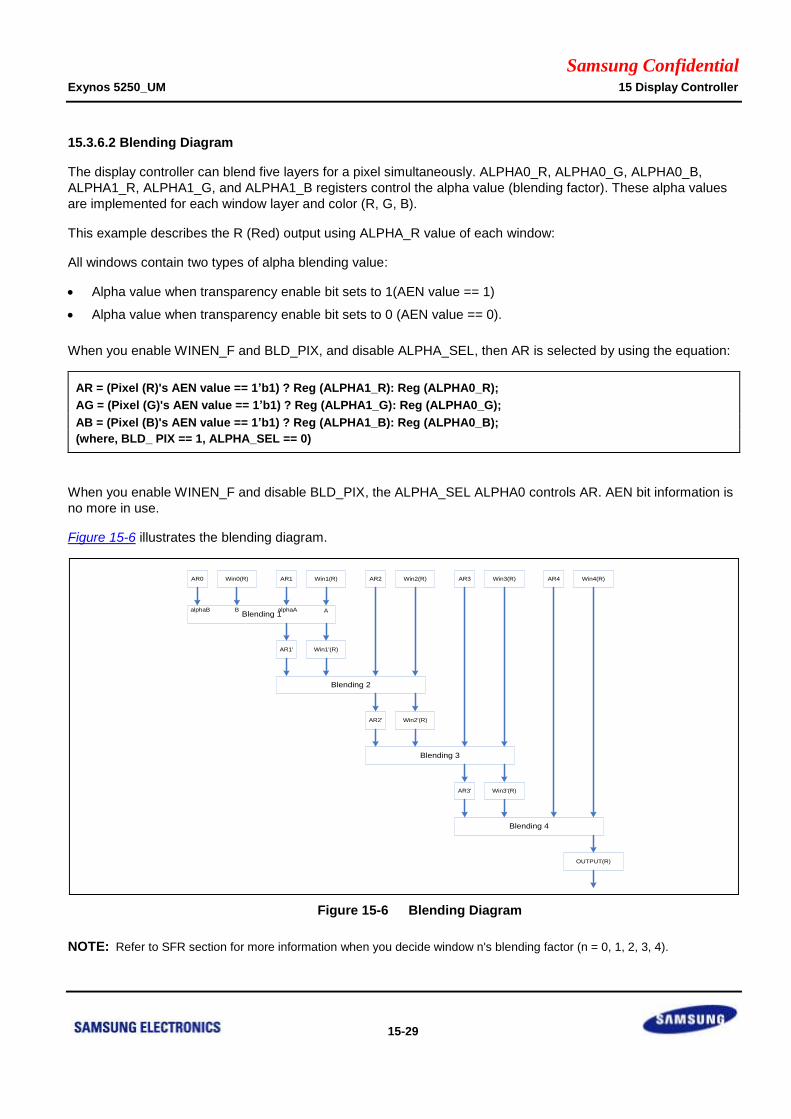
Samsung Confidential Exynos 5250_UM 15 Display Controller
15-29
15.3.6.2 Blending Diagram
The display controller can blend five layers for a pixel simultaneously. ALPHA0_R, ALPHA0_G, ALPHA0_B,
ALPHA1_R, ALPHA1_G, and ALPHA1_B registers control the alpha value (blending factor). These alpha values
are implemented for each window layer and color (R, G, B).
This example describes the R (Red) output using ALPHA_R value of each window:
All windows contain two types of alpha blending value:
Alpha value when transparency enable bit sets to 1(AEN value == 1)
Alpha value when transparency enable bit sets to 0 (AEN value == 0).
When you enable WINEN_F and BLD_PIX, and disable ALPHA_SEL, then AR is selected by using the equation:
AR = (Pixel (R)'s AEN value == 1’b1) ? Reg (ALPHA1_R): Reg (ALPHA0_R);
AG = (Pixel (G)'s AEN value == 1’b1) ? Reg (ALPHA1_G): Reg (ALPHA0_G);
AB = (Pixel (B)'s AEN value == 1’b1) ? Reg (ALPHA1_B): Reg (ALPHA0_B);
(where, BLD_ PIX == 1, ALPHA_SEL == 0)
When you enable WINEN_F and disable BLD_PIX, the ALPHA_SEL ALPHA0 controls AR. AEN bit information is
no more in use.
Figure 15-6 illustrates the blending diagram.
Figure 15-6 Blending Diagram
NOTE: Refer to SFR section for more information when you decide window n's blending factor (n = 0, 1, 2, 3, 4).
AR0 Win0(R) AR1 Win1(R) AR2 Win2(R) AR3 Win3(R) AR4 Win4(R)
Blending 1
AR1' Win1'(R)
Blending 2
AR2' Win2'(R)
Blending 3
AR3' Win3'(R)
Blending 4
OUTPUT(R)
alphaAalphaB AB
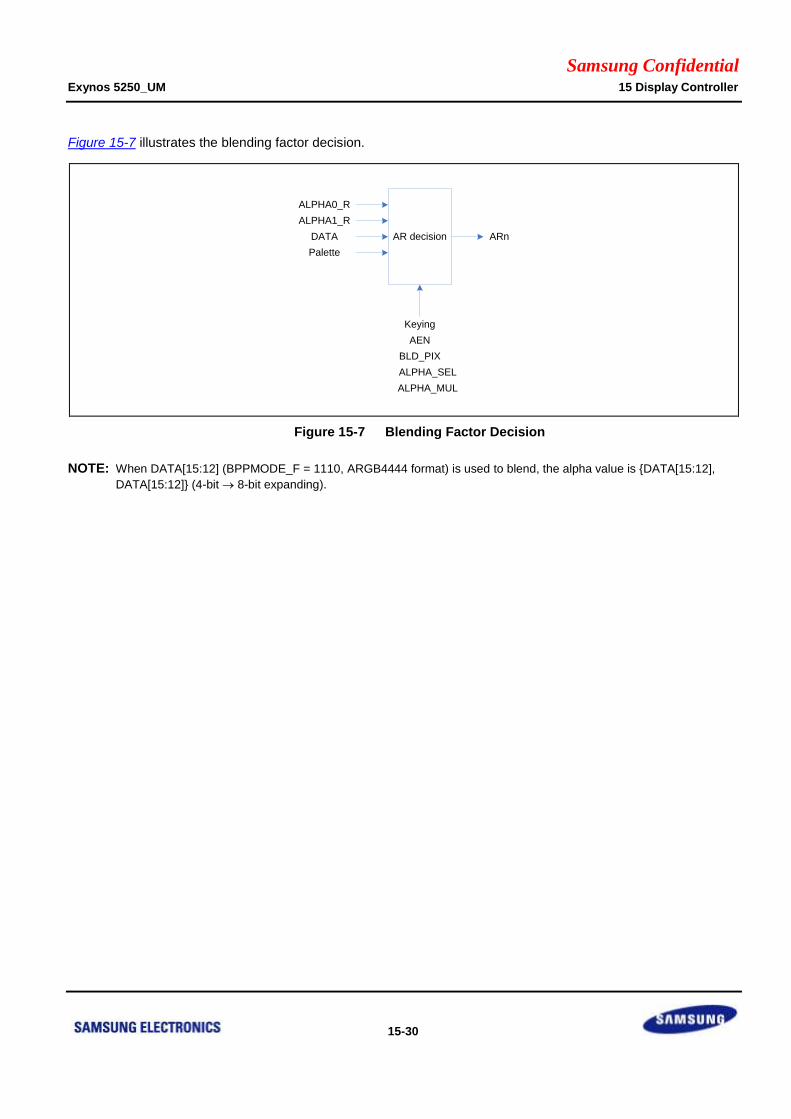
Samsung Confidential Exynos 5250_UM 15 Display Controller
15-30
Figure 15-7 illustrates the blending factor decision.
Figure 15-7 Blending Factor Decision
NOTE: When DATA[15:12] (BPPMODE_F = 1110, ARGB4444 format) is used to blend, the alpha value is {DATA[15:12],
DATA[15:12]} (4-bit 8-bit expanding).
AR decision ARn
ALPHA0_R
ALPHA1_R
DATA
Palette
Keying
AEN
BLD_PIX
ALPHA_SEL
ALPHA_MUL
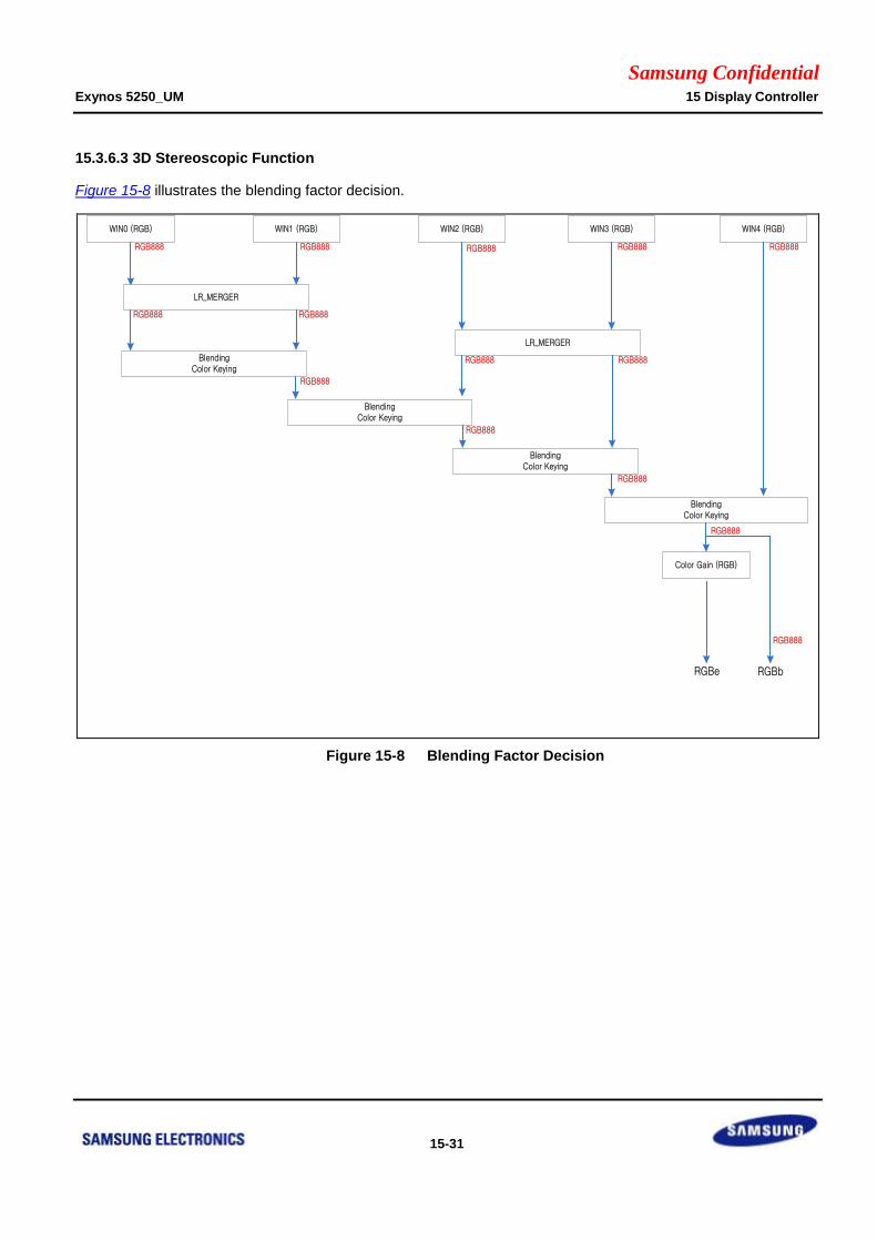
Samsung Confidential Exynos 5250_UM 15 Display Controller
15-31
15.3.6.3 3D Stereoscopic Function
Figure 15-8 illustrates the blending factor decision.
WIN0 (RGB) WIN1 (RGB) WIN2 (RGB) WIN3 (RGB) WIN4 (RGB)
BlendingColor Keying
BlendingColor Keying
BlendingColor Keying
BlendingColor Keying
Color Gain (RGB)
RGBe
RGB888 RGB888 RGB888 RGB888 RGB888
RGB888
RGB888
RGB888
RGB888
RGBb
RGB888
LR_MERGER
RGB888 RGB888
LR_MERGER
RGB888 RGB888
Figure 15-8 Blending Factor Decision
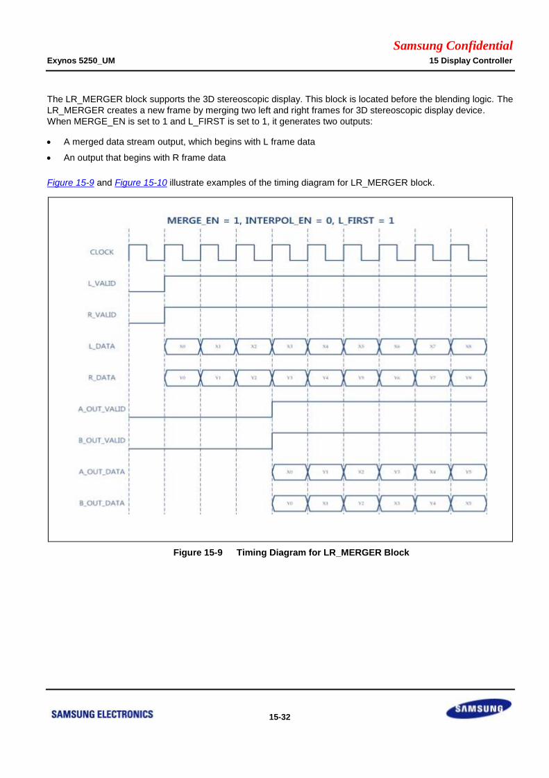
Samsung Confidential Exynos 5250_UM 15 Display Controller
15-32
The LR_MERGER block supports the 3D stereoscopic display. This block is located before the blending logic. The
LR_MERGER creates a new frame by merging two left and right frames for 3D stereoscopic display device.
When MERGE_EN is set to 1 and L_FIRST is set to 1, it generates two outputs:
A merged data stream output, which begins with L frame data
An output that begins with R frame data
Figure 15-9 and Figure 15-10 illustrate examples of the timing diagram for LR_MERGER block.
Figure 15-9 Timing Diagram for LR_MERGER Block
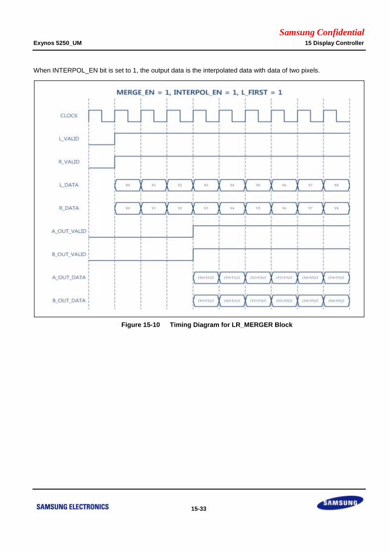
Samsung Confidential Exynos 5250_UM 15 Display Controller
15-33
When INTERPOL_EN bit is set to 1, the output data is the interpolated data with data of two pixels.
Figure 15-10 Timing Diagram for LR_MERGER Block
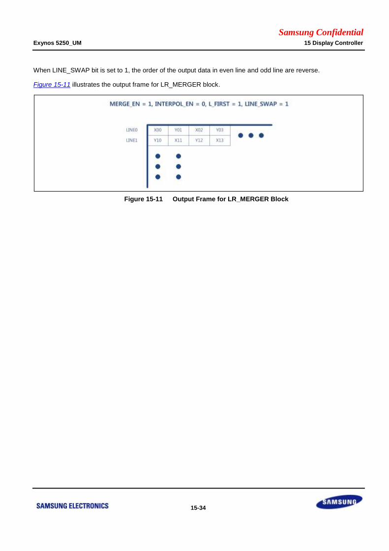
Samsung Confidential Exynos 5250_UM 15 Display Controller
15-34
When LINE_SWAP bit is set to 1, the order of the output data in even line and odd line are reverse.
Figure 15-11 illustrates the output frame for LR_MERGER block.
Figure 15-11 Output Frame for LR_MERGER Block
Samsung Confidential Exynos 5250_UM 15 Display Controller
15-35
15.3.6.4 Color Key Function
The Color Key function in display controller supports various effects for image mapping. For special functionality,
the background image substitutes the Color Key register that specifies the color image of OSD layer. It substitutes
the Color Key register, either as a cursor image of the camera, or as a preview image of the camera.
Figure 15-12 illustrates the configuration of Color Key function.
Figure 15-12 Color Key Function Configurations
W indow 3
W indow 1OSD image 180 x 100
BG image 320 x 240
W indow 1
BLEND
(ALPHA = 0x7F)
W indow 1
BLEND
(ALPHA = 0xFF)
W indow 1
BLEND
(ALPHA = 0x00)
W indow 3 W indow 3
W indow 1
Chroma-Key (KEY_BLEN)
(KEY_ALPHA = 0xFF)
W indow 3
W indow 1
Chroma-Key (KEY_BLEN)
(KEY_ALPHA = 0x7F)
W indow 3
W indow 1
W indow 3
W indow 1
Chroma-Key (not KEY_BLEN)
W indow 3
Chroma-Key (KEY_BLEN)
(KEY_ALPHA = 0x00)
Samsung Confidential Exynos 5250_UM 15 Display Controller
15-36
15.3.6.5 Blending and Color-Key Function
The display controller supports simultaneous blending function. It supports two transparency factors and Color
Key function in the same window.
Figure 15-13 illustrates the Blending and Color Key function.
Window 1Window 0
Sub - menu
Chroma-key
Alpha 0 (50%)
Alpha 1 (100%)
Sub - menu
Sub - menu
Main Menu
Camera
Memo
08:23
Main Menu
Camera
Memo
08:23
Figure 15-13 Blending and Color-Key Function
Samsung Confidential Exynos 5250_UM 15 Display Controller
15-37
Figure 15-14 illustrates the blending decision diagram.
KEY_ EN ?
Start
a = 1 (max)
b = 0
N
Color matchY N
< Blending Equation Decision >
KEY_ BLEN ?
a = alphaA
b = 1 - alphaA
Y
N
Y
DIRCONY
N
Y
a = 0
b = 1 (max)
a = A _FUNC
b = B_ FUNC
End
Blending & Chroma- keying
alphaAalphaB AB
alphaB’ B’
Equation
Decision
Transparency
Factor
Decision
Data
Formatter
Transparency
Factor
Decision
Data
Formatter
KEY_ EN ?
Start
0
N
Color matchY N
< Transparency factor Decision >
KEY_ BLEN ?
KEY_ALPHA
Y
N
Y
BLD_ PIX = 1
ALPHA_SEL
Y
ALPHA_SEL
Only when ‘ARGB’
N
ALPHA_1
ALPHA_0
N
N
Y
Y
BPPMODE
[3:2 ] = 00 Y
WxPAL = 111
DATA[31:24]
YN
AENN
ALPHA_1
ALPHA_0
Y
Palette
N
BLEN_NEW
{ DATA[27:24]
,DATA[27:24]}
N
DATA[31:24]
Y
ALPHA_MULYN
App * ALPHA0
Ap
Ap
App
N
Y
App * ({ ALPHA0[7:4],
ALPHA0[7:4]})
Ap
Ap
Ap
Ap
Ap
Ap
Ap
BLEN_NEW
{ Ap [7:4],Ap[ 7:4]}Ap [7:0]
App App
BLEN_NEW
Ap
Only valid
@ ( BLD_ PIX = 1 && ALPHA_ SEL = 1
&& ( BPPMODE == 1101 or 1110) )
End
App
Transparency factor
Figure 15-14 Blending Decision Diagram
Samsung Confidential Exynos 5250_UM 15 Display Controller
15-38
15.3.7 Image Enhancement
15.3.7.1 Overview
The main function of the VPRCS module is image enhancement. The display controller supports these functions:
Color Gain
Figure 15-15 illustrates the image enhancement flow.
CSCY2R BLENDING RGB I/F
RGB
YCbCr
Image
Enhancement
Block
Color Gain
RGB space YCbCr space
WB IF
LIMITTER
Figure 15-15 Image Enhancement Flow
15.3.7.2 Color Gain Control
Color Gain Control consists of three registers for each color: Red, Green, and Blue. The maximum value of color
gain is 3.99609375 (approximately 4). It contains 8-bit resolution.
R (color gain) = R CG_RGAIN
G (color gain) = G CG_GGAIN
B (color gain) = B CG_BGAIN
CG_R (G, B) GAIN consists of 2-bit integer and 8-bit fraction. The maximum value of color gain is approximately 4
with 8-bit resolution.
The output value saturates at 255.
Samsung Confidential Exynos 5250_UM 15 Display Controller
15-39
15.3.8 VTIME Controller
VTIME comprises of two blocks, namely:
VTIME_RGB_TV for RGB timing control
VTIME_I80 for indirect i80 interface timing control
15.3.8.1 RGB Interface Controller
VTIME generates control signals for the RGB interface:
RGB_VSYNC
RGB_HSYNC
RGB_VDEN
RGB_VCLK
These control signals configure the VIDTCON0/1/2 registers in the VSFR register.
The VTIME module generates programmable control signals that support various display devices. These control
signals are based on the programmable configuration of display control registers in the VSFR. The LCD line
pointer moves to the first pixel of the top of display. The configuration of HOZVAL field and LINEVAL registers,
control the pulse generation, of RGB_VSYNC and RGB_HSYNC, respectively. The size of the LCD panel
considers this equation to determine HOZVAL and LINEVAL:
HOZVAL = (Horizontal display size) – 1
LINEVAL = (Vertical display size) – 1
The CLKVAL field in VIDCON0 register controls the rate of RGB_VCLK signal. Table 15-5 describes the
relationship between RGB_VCLK and CLKVAL. The minimum value of CLKVAL is 1.
RGB_VCLK (Hz) = H CLK/(CLKVAL + 1), where CLKVAL >= 1
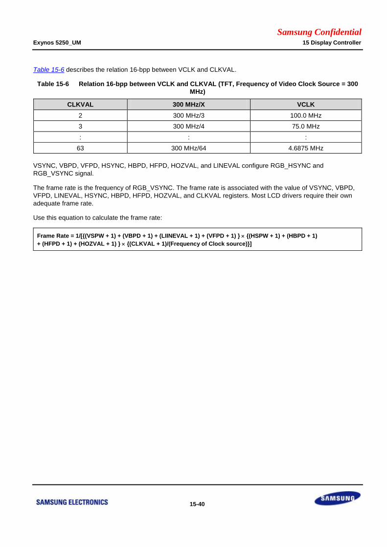
Samsung Confidential Exynos 5250_UM 15 Display Controller
15-40
Table 15-6 describes the relation 16-bpp between VCLK and CLKVAL.
Table 15-6 Relation 16-bpp between VCLK and CLKVAL (TFT, Frequency of Video Clock Source = 300
MHz)
CLKVAL 300 MHz/X VCLK
2 300 MHz/3 100.0 MHz
3 300 MHz/4 75.0 MHz
: : :
63 300 MHz/64 4.6875 MHz
VSYNC, VBPD, VFPD, HSYNC, HBPD, HFPD, HOZVAL, and LINEVAL configure RGB_HSYNC and
RGB_VSYNC signal.
The frame rate is the frequency of RGB_VSYNC. The frame rate is associated with the value of VSYNC, VBPD,
VFPD, LINEVAL, HSYNC, HBPD, HFPD, HOZVAL, and CLKVAL registers. Most LCD drivers require their own
adequate frame rate.
Use this equation to calculate the frame rate:
Frame Rate = 1/[{(VSPW + 1) + (VBPD + 1) + (LIINEVAL + 1) + (VFPD + 1) } {(HSPW + 1) + (HBPD + 1)
+ (HFPD + 1) + (HOZVAL + 1) } {(CLKVAL + 1)/(Frequency of Clock source)}]

Samsung Confidential Exynos 5250_UM 15 Display Controller
15-41
15.3.8.2 I80 Interface Controller
VTIME_I80 controls display controller for CPU style LDI. It has the following functions:
Generates I80 Interface Control Signals
CPU style LDI Command Control
Timing Control for VDMA and VDPRCS
15.3.8.3 Output Control Signal Generation
VTIME_I80 generates SYS_CS0, SYS_CS1, SYS_WE, and SYS_RS control signals (For Timing Diagram, refer
to Figure 15-19). Their timing parameters, LCD_CS_SETUP, LCD_WR_SETUP, LCD_WR_ACT, and
LCD_WR_HOLD are set through I80IFCONA0 and I80IFCONA1 SFRs.
15.3.8.4 Partial Display Control
Although partial display is the main feature of CPU style LDI, VTIME_I80 does not support this function in
hardware logic.
This function is implemented by SFR setting (LINEVAL, HOZVAL, OSD_LeftTopX_F, OSD_LeftTopY_F,
OSD_RightBotX_F, OSD_RightBotY_F, PAGEWIDTH, and OFFSIZE).
15.3.8.5 LDI Command Control
LDI receives both command and data. Command specifies an index for selecting the SFR in LDI. In control signal
for command and data, only SYS_RS signal has a special function. Usually, SYS_RS has a polarity of "1" for
issuing command and vice versa.
Display controller has one command control:
Normal command

Samsung Confidential Exynos 5250_UM 15 Display Controller
15-42
15.3.9 Setting of Commands
15.3.9.1 Normal Command
To execute Normal command, follow these steps:
Put commands into LDI_CMD0 to 11 (maximum 12 commands).
Set CMDx_EN in LDI_CMDCON0 to enable normal command (For example, if you want to enable command 4,
you have to set CMD4_EN to 0x01).
Set NORMAL_CMD_ST in I80IFCONB0/1.
The display controller has the following characteristics for command operations:
Normal command mode is possible for each of the 12 commands.
Sends 12 maximum commands between frames in its normal operation (Normal operation means ENVID = 1
and video data is displayed in LCD panel).
Issues commands in the order of CMD0 CMD1 CMD2 CMD3 … CMD10 CMD11.
Skips disabled commands (CMDx_EN = 0x0).
Sends over 12 commands (Possible in Normal command and system initialization).
Set 12 LDI_CMDx, CMDx_EN, and CMDx_RS.
Set NORMAL_CMD_ST.
Read NORMAL_CMD_ST with polling. If 0, go to NORMAL_CMD_ST setting.
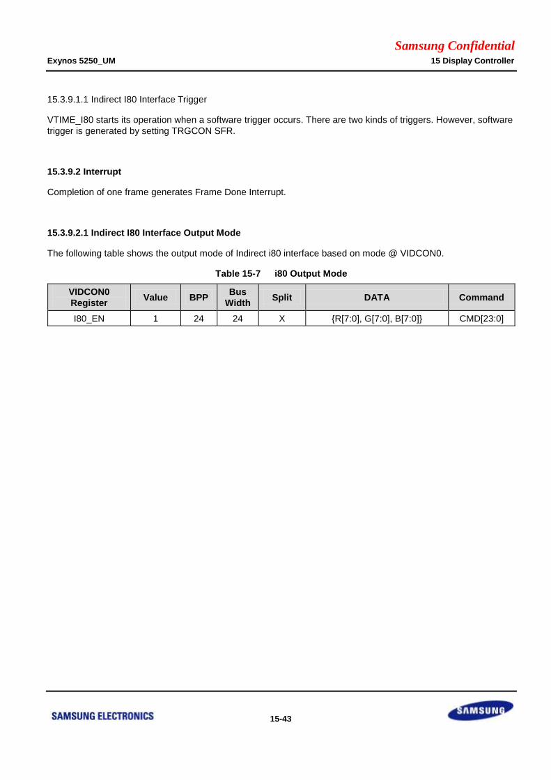
Samsung Confidential Exynos 5250_UM 15 Display Controller
15-43
15.3.9.1.1 Indirect I80 Interface Trigger
VTIME_I80 starts its operation when a software trigger occurs. There are two kinds of triggers. However, software
trigger is generated by setting TRGCON SFR.
15.3.9.2 Interrupt
Completion of one frame generates Frame Done Interrupt.
15.3.9.2.1 Indirect I80 Interface Output Mode
The following table shows the output mode of Indirect i80 interface based on mode @ VIDCON0.
Table 15-7 i80 Output Mode
VIDCON0
Register Value BPP
Bus
Width Split DATA Command
I80_EN 1 24 24 X {R[7:0], G[7:0], B[7:0]} CMD[23:0]
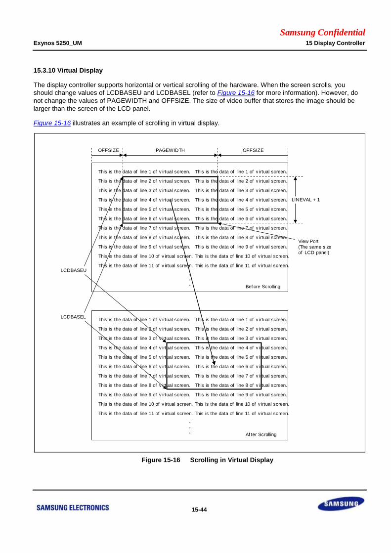
Samsung Confidential Exynos 5250_UM 15 Display Controller
15-44
15.3.10 Virtual Display
The display controller supports horizontal or vertical scrolling of the hardware. When the screen scrolls, you
should change values of LCDBASEU and LCDBASEL (refer to Figure 15-16 for more information). However, do
not change the values of PAGEWIDTH and OFFSIZE. The size of video buffer that stores the image should be
larger than the screen of the LCD panel.
Figure 15-16 illustrates an example of scrolling in virtual display.
Figure 15-16 Scrolling in Virtual Display
This is the data of line 1 of v irtual screen. This is the data of line 1 of v irtual screen.
This is the data of line 2 of v irtual screen. This is the data of line 2 of v irtual screen.
This is the data of line 3 of v irtual screen. This is the data of line 3 of v irtual screen.
This is the data of line 4 of v irtual screen. This is the data of line 4 of v irtual screen.
This is the data of line 5 of v irtual screen. This is the data of line 5 of v irtual screen.
This is the data of line 6 of v irtual screen. This is the data of line 6 of v irtual screen.
This is the data of line 7 of v irtual screen. This is the data of line 7 of v irtual screen.
This is the data of line 8 of v irtual screen. This is the data of line 8 of v irtual screen.
This is the data of line 9 of v irtual screen. This is the data of line 9 of v irtual screen.
This is the data of line 10 of v irtual screen. This is the data of line 10 of v irtual screen.
This is the data of line 11 of v irtual screen. This is the data of line 11 of v irtual screen....
Bef ore Scrolling
View Port
(The same size
of LCD panel)
LINEVAL + 1
OFFSIZEPAGEWIDTH
This is the data of line 1 of v irtual screen. This is the data of line 1 of v irtual screen.
This is the data of line 2 of v irtual screen. This is the data of line 2 of v irtual screen.
This is the data of line 3 of v irtual screen. This is the data of line 3 of v irtual screen.
This is the data of line 4 of v irtual screen. This is the data of line 4 of v irtual screen.
This is the data of line 5 of v irtual screen. This is the data of line 5 of v irtual screen.
This is the data of line 6 of v irtual screen. This is the data of line 6 of v irtual screen.
This is the data of line 7 of v irtual screen. This is the data of line 7 of v irtual screen.
This is the data of line 8 of v irtual screen. This is the data of line 8 of v irtual screen.
This is the data of line 9 of v irtual screen. This is the data of line 9 of v irtual screen.
This is the data of line 10 of v irtual screen. This is the data of line 10 of v irtual screen.
This is the data of line 11 of v irtual screen. This is the data of line 11 of v irtual screen.
.
.
.
Af ter Scrolling
LCDBASEU
LCDBASEL
OFFSIZE
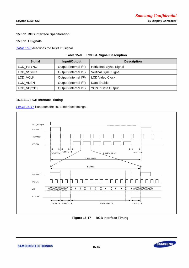
Samsung Confidential Exynos 5250_UM 15 Display Controller
15-45
15.3.11 RGB Interface Specification
15.3.11.1 Signals
Table 15-8 describes the RGB I/F signal.
Table 15-8 RGB I/F Signal Description
Signal Input/Output Description
LCD_HSYNC Output (Internal I/F) Horizontal Sync. Signal
LCD_VSYNC Output (Internal I/F) Vertical Sync. Signal
LCD_VCLK Output (Internal I/F) LCD Video Clock
LCD_VDEN Output (Internal I/F) Data Enable
LCD_VD[23:0] Output (Internal I/F) YCbCr Data Output
15.3.11.2 RGB Interface Timing
Figure 15-17 illustrates the RGB interface timings.
Figure 15-17 RGB Interface Timing
VSYNC
HSYNC
VDEN
VSPW+1VBPD+1 VFPD+1LINEVAL+1
1 FRAME
VDEN
HSPW+1 HBPD+1 HFPD+1HOZVAL+1
HSYNC
VCLK
VD
1 LINE
INT_FrSyn
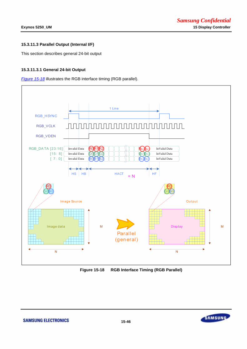
Samsung Confidential Exynos 5250_UM 15 Display Controller
15-46
15.3.11.3 Parallel Output (Internal I/F)
This section describes general 24-bit output
15.3.11.3.1 General 24-bit Output
Figure 15-18 illustrates the RGB interface timing (RGB parallel).
Figure 15-18 RGB Interface Timing (RGB Parallel)
InValid DataInvalid Data
RGB_HSYNC
RGB_VCLK
RGB_DA TA [23:16]
RGB_VDEN
HACT HFHBHS
1 Line
Display
N
M
R0
G0 B0
Image dat a
N
M
Image Source Out put
Parallel
(general)
R0
G0 B0
InValid DataInvalid Data
InValid DataInvalid Data
[15: 8]
[ 7: 0]
R0
G0
B0 BN-1
RN-1
GN-1
R1
G1
B1
R2
G2
B2
RN-2
GN-2
BN-2
= N
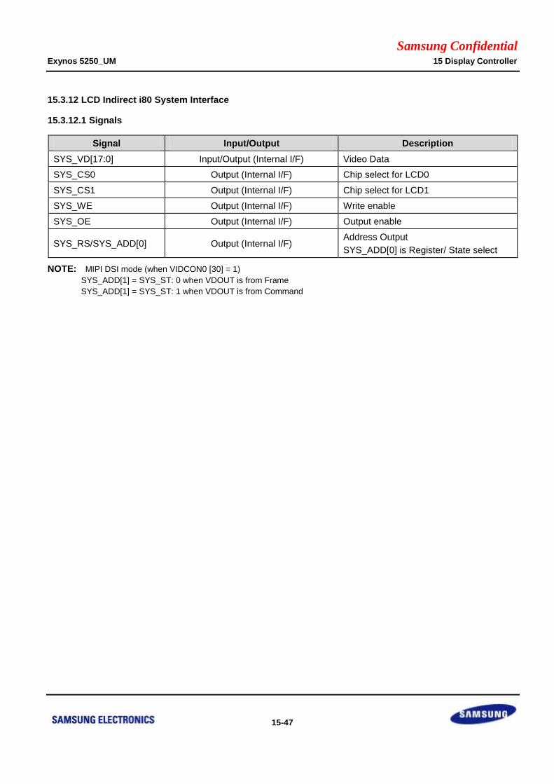
Samsung Confidential Exynos 5250_UM 15 Display Controller
15-47
15.3.12 LCD Indirect i80 System Interface
15.3.12.1 Signals
Signal Input/Output Description
SYS_VD[17:0] Input/Output (Internal I/F) Video Data
SYS_CS0 Output (Internal I/F) Chip select for LCD0
SYS_CS1 Output (Internal I/F) Chip select for LCD1
SYS_WE Output (Internal I/F) Write enable
SYS_OE Output (Internal I/F) Output enable
SYS_RS/SYS_ADD[0] Output (Internal I/F) Address Output
SYS_ADD[0] is Register/ State select
NOTE: MIPI DSI mode (when VIDCON0 [30] = 1)
SYS_ADD[1] = SYS_ST: 0 when VDOUT is from Frame
SYS_ADD[1] = SYS_ST: 1 when VDOUT is from Command
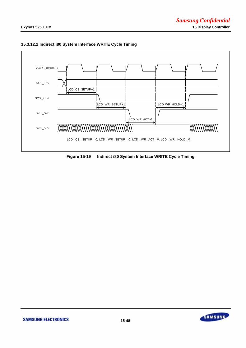
Samsung Confidential Exynos 5250_UM 15 Display Controller
15-48
15.3.12.2 Indirect i80 System Interface WRITE Cycle Timing
Figure 15-19 Indirect i80 System Interface WRITE Cycle Timing
LCD_CS_SETUP+1
LCD_WR_SETUP+1
LCD_WR_ACT+1
LCD_WR_HOLD+1
VCLK (internal )
SYS _ RS
SYS _CSn
SYS _ WE
SYS _ VD
LCD _CS _ SETUP = 0, LCD _ WR _SETUP = 0, LCD _WR _ACT =0 , LCD _WR _ HOLD =0

Samsung Confidential Exynos 5250_UM 15 Display Controller
15-49
15.4 Programmer's Model
15.4.1 Overview
Registers to configure the display controller:
1. VIDCON0: Configures video output format and displays enable/disable
2. VIDCON1: Specifies the RGB I/F control signal
3. VIDCON2: Specifies the output data format control
4. VIDCON3: Specifies the image enhancement control
5. I80IFCONx: Specifies CPU interface control signal.
6. VIDTCONx: Configures video output timing and determines the size of display
7. WINCONx: Specifies the setting of each window feature
8. VIDOSDxA, VIDOSDxB: Specifies the setting of each window position
9. VIDOSDxC,D: Specifies the setting of OSD size
10. VIDWxALPHA0/1: Specifies the setting of alpha value
11. BLENDEQx: Specifies the setting of blending equation
12. VIDWxxADDx: Specifies the setting of source image address
13. WxKEYCONx: Specifies the Color Key Setting register
14. WxKEYALPHA: Specifies the setting of color key alpha value
15. WINxMAP: Specifies the window color control
16. COLORGAINCON: Specifies the setting of color gain value
17. WPALCON: Specifies the Palette Control register
18. WxPDATAxx: Specifies the window palette data of each index
19. SHDOWCON: Specifies the Shadow Control register

Samsung Confidential Exynos 5250_UM 15 Display Controller
15-50
15.5 Register Description
15.5.1 Register Map Summary
Base Address: 0x1440_0000
Register Offset Description Reset Value
MIXER Registers
VIDCON0 0x0000 Specifies the video control 0 register 0x0000_0000
VIDCON2 0x0008 Specifies the video control 2 register 0x0000_0000
VIDCON3 0x000C Specifies the video control 3 register 0x0000_0000
WINCON0 0x0020 Specifies the window control 0 register 0x0000_0000
WINCON1 0x0024 Specifies the window control 1 register 0x0000_0000
WINCON2 0x0028 Specifies the window control 2 register 0x0000_0000
WINCON3 0x002C Specifies the window control 3 register 0x0000_0000
WINCON4 0x0030 Specifies the window control 4 register 0x0000_0000
SHADOWCON 0x0034 Specifies the window shadow control register 0x0000_0000
VIDOSD0A 0x0040 Specifies the video window 0 position control register 0x0000_0000
VIDOSD0B 0x0044 Specifies the video window 0 position control register 0x0000_0000
VIDOSD0C 0x0048 Specifies the video window 0 size control register 0x0000_0000
VIDOSD1A 0x0050 Specifies the video window 1 position control register 0x0000_0000
VIDOSD1B 0x0054 Specifies the video window 1 position control register 0x0000_0000
VIDOSD1C 0x0058 Specifies the video window 1 alpha control register 0x0000_0000
VIDOSD1D 0x005C Specifies the video window 1 size control register 0x0000_0000
VIDOSD2A 0x0060 Specifies the video window 2 position control register 0x0000_0000
VIDOSD2B 0x0064 Specifies the video window 2 position control register 0x0000_0000
VIDOSD2C 0x0068 Specifies the video window 2 alpha control register 0x0000_0000
VIDOSD2D 0x006C Specifies the video window 2 size control register 0x0000_0000
VIDOSD3A 0x0070 Specifies the video window 3 position control register 0x0000_0000
VIDOSD3B 0x0074 Specifies the video window 3 position control register 0x0000_0000
VIDOSD3C 0x0078 Specifies the video window 3 alpha control register 0x0000_0000
VIDOSD4A 0x0080 Specifies the video window 4 position control register 0x0000_0000
VIDOSD4B 0x0084 Specifies the video window 4 position control register 0x0000_0000
VIDOSD4C 0x0088 Specifies the video window 4 alpha control register 0x0000_0000
VIDW00ADD0B0 0x00A0 Specifies the window 0 buffer start address register, buffer 0 0x0000_0000
VIDW00ADD0B1 0x00A4 Specifies the window 0 buffer start address register, buffer 1 0x0000_0000
VIDW00ADD0B2 0x20A0 Specifies the window 0 buffer start address register, buffer 2 0x0000_0000
VIDW01ADD0B0 0x00A8 Specifies the window 1 buffer start address register, buffer 0 0x0000_0000
VIDW01ADD0B1 0x00AC Specifies the window 1 buffer start address register, buffer 1 0x0000_0000
VIDW01ADD0B2 0x20A8 Specifies the window 1 buffer start address register, buffer 2 0x0000_0000
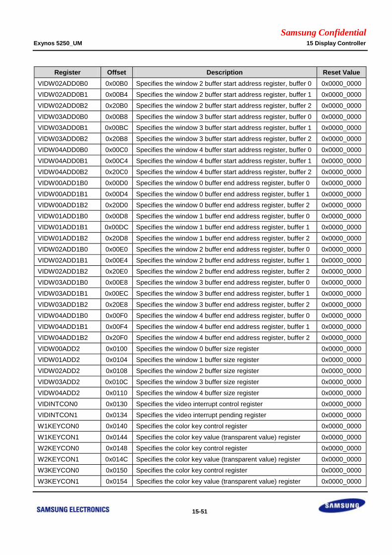
Samsung Confidential Exynos 5250_UM 15 Display Controller
15-51
Register Offset Description Reset Value
VIDW02ADD0B0 0x00B0 Specifies the window 2 buffer start address register, buffer 0 0x0000_0000
VIDW02ADD0B1 0x00B4 Specifies the window 2 buffer start address register, buffer 1 0x0000_0000
VIDW02ADD0B2 0x20B0 Specifies the window 2 buffer start address register, buffer 2 0x0000_0000
VIDW03ADD0B0 0x00B8 Specifies the window 3 buffer start address register, buffer 0 0x0000_0000
VIDW03ADD0B1 0x00BC Specifies the window 3 buffer start address register, buffer 1 0x0000_0000
VIDW03ADD0B2 0x20B8 Specifies the window 3 buffer start address register, buffer 2 0x0000_0000
VIDW04ADD0B0 0x00C0 Specifies the window 4 buffer start address register, buffer 0 0x0000_0000
VIDW04ADD0B1 0x00C4 Specifies the window 4 buffer start address register, buffer 1 0x0000_0000
VIDW04ADD0B2 0x20C0 Specifies the window 4 buffer start address register, buffer 2 0x0000_0000
VIDW00ADD1B0 0x00D0 Specifies the window 0 buffer end address register, buffer 0 0x0000_0000
VIDW00ADD1B1 0x00D4 Specifies the window 0 buffer end address register, buffer 1 0x0000_0000
VIDW00ADD1B2 0x20D0 Specifies the window 0 buffer end address register, buffer 2 0x0000_0000
VIDW01ADD1B0 0x00D8 Specifies the window 1 buffer end address register, buffer 0 0x0000_0000
VIDW01ADD1B1 0x00DC Specifies the window 1 buffer end address register, buffer 1 0x0000_0000
VIDW01ADD1B2 0x20D8 Specifies the window 1 buffer end address register, buffer 2 0x0000_0000
VIDW02ADD1B0 0x00E0 Specifies the window 2 buffer end address register, buffer 0 0x0000_0000
VIDW02ADD1B1 0x00E4 Specifies the window 2 buffer end address register, buffer 1 0x0000_0000
VIDW02ADD1B2 0x20E0 Specifies the window 2 buffer end address register, buffer 2 0x0000_0000
VIDW03ADD1B0 0x00E8 Specifies the window 3 buffer end address register, buffer 0 0x0000_0000
VIDW03ADD1B1 0x00EC Specifies the window 3 buffer end address register, buffer 1 0x0000_0000
VIDW03ADD1B2 0x20E8 Specifies the window 3 buffer end address register, buffer 2 0x0000_0000
VIDW04ADD1B0 0x00F0 Specifies the window 4 buffer end address register, buffer 0 0x0000_0000
VIDW04ADD1B1 0x00F4 Specifies the window 4 buffer end address register, buffer 1 0x0000_0000
VIDW04ADD1B2 0x20F0 Specifies the window 4 buffer end address register, buffer 2 0x0000_0000
VIDW00ADD2 0x0100 Specifies the window 0 buffer size register 0x0000_0000
VIDW01ADD2 0x0104 Specifies the window 1 buffer size register 0x0000_0000
VIDW02ADD2 0x0108 Specifies the window 2 buffer size register 0x0000_0000
VIDW03ADD2 0x010C Specifies the window 3 buffer size register 0x0000_0000
VIDW04ADD2 0x0110 Specifies the window 4 buffer size register 0x0000_0000
VIDINTCON0 0x0130 Specifies the video interrupt control register 0x0000_0000
VIDINTCON1 0x0134 Specifies the video interrupt pending register 0x0000_0000
W1KEYCON0 0x0140 Specifies the color key control register 0x0000_0000
W1KEYCON1 0x0144 Specifies the color key value (transparent value) register 0x0000_0000
W2KEYCON0 0x0148 Specifies the color key control register 0x0000_0000
W2KEYCON1 0x014C Specifies the color key value (transparent value) register 0x0000_0000
W3KEYCON0 0x0150 Specifies the color key control register 0x0000_0000
W3KEYCON1 0x0154 Specifies the color key value (transparent value) register 0x0000_0000
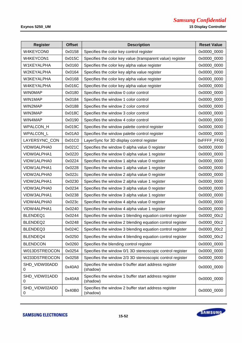
Samsung Confidential Exynos 5250_UM 15 Display Controller
15-52
Register Offset Description Reset Value
W4KEYCON0 0x0158 Specifies the color key control register 0x0000_0000
W4KEYCON1 0x015C Specifies the color key value (transparent value) register 0x0000_0000
W1KEYALPHA 0x0160 Specifies the color key alpha value register 0x0000_0000
W2KEYALPHA 0x0164 Specifies the color key alpha value register 0x0000_0000
W3KEYALPHA 0x0168 Specifies the color key alpha value register 0x0000_0000
W4KEYALPHA 0x016C Specifies the color key alpha value register 0x0000_0000
WIN0MAP 0x0180 Specifies the window 0 color control 0x0000_0000
WIN1MAP 0x0184 Specifies the window 1 color control 0x0000_0000
WIN2MAP 0x0188 Specifies the window 2 color control 0x0000_0000
WIN3MAP 0x018C Specifies the window 3 color control 0x0000_0000
WIN4MAP 0x0190 Specifies the window 4 color control 0x0000_0000
WPALCON_H 0x019C Specifies the window palette control register 0x0000_0000
WPALCON_L 0x01A0 Specifies the window palette control register 0x0000_0000
LAYERSYNC_CON 0x01C0 LayerSync for 3D display control register 0xFFFF_FF00
VIDW0ALPHA0 0x021C Specifies the window 0 alpha value 0 register 0x0000_0000
VIDW0ALPHA1 0x0220 Specifies the window 0 alpha value 1 register 0x0000_0000
VIDW1ALPHA0 0x0224 Specifies the window 1 alpha value 0 register 0x0000_0000
VIDW1ALPHA1 0x0228 Specifies the window 1 alpha value 1 register 0x0000_0000
VIDW2ALPHA0 0x022c Specifies the window 2 alpha value 0 register 0x0000_0000
VIDW2ALPHA1 0x0230 Specifies the window 2 alpha value 1 register 0x0000_0000
VIDW3ALPHA0 0x0234 Specifies the window 3 alpha value 0 register 0x0000_0000
VIDW3ALPHA1 0x0238 Specifies the window 3 alpha value 1 register 0x0000_0000
VIDW4ALPHA0 0x023c Specifies the window 4 alpha value 0 register 0x0000_0000
VIDW4ALPHA1 0x0240 Specifies the window 4 alpha value 1 register 0x0000_0000
BLENDEQ1 0x0244 Specifies the window 1 blending equation control register 0x0000_00c2
BLENDEQ2 0x0248 Specifies the window 2 blending equation control register 0x0000_00c2
BLENDEQ3 0x024C Specifies the window 3 blending equation control register 0x0000_00c2
BLENDEQ4 0x0250 Specifies the window 4 blending equation control register 0x0000_00c2
BLENDCON 0x0260 Specifies the blending control register 0x0000_0000
W013DSTREOCON 0x0254 Specifies the window 0/1 3D stereoscopic control register 0x0000_0000
W233DSTREOCON 0x0258 Specifies the window 2/3 3D stereoscopic control register 0x0000_0000
SHD_VIDW00ADD
0 0x40A0
Specifies the window 0 buffer atart address register
(shadow) 0x0000_0000
SHD_VIDW01ADD
0 0x40A8
Specifies the window 1 buffer start address register
(shadow) 0x0000_0000
SHD_VIDW02ADD
0 0x40B0
Specifies the window 2 buffer start address register
(shadow) 0x0000_0000
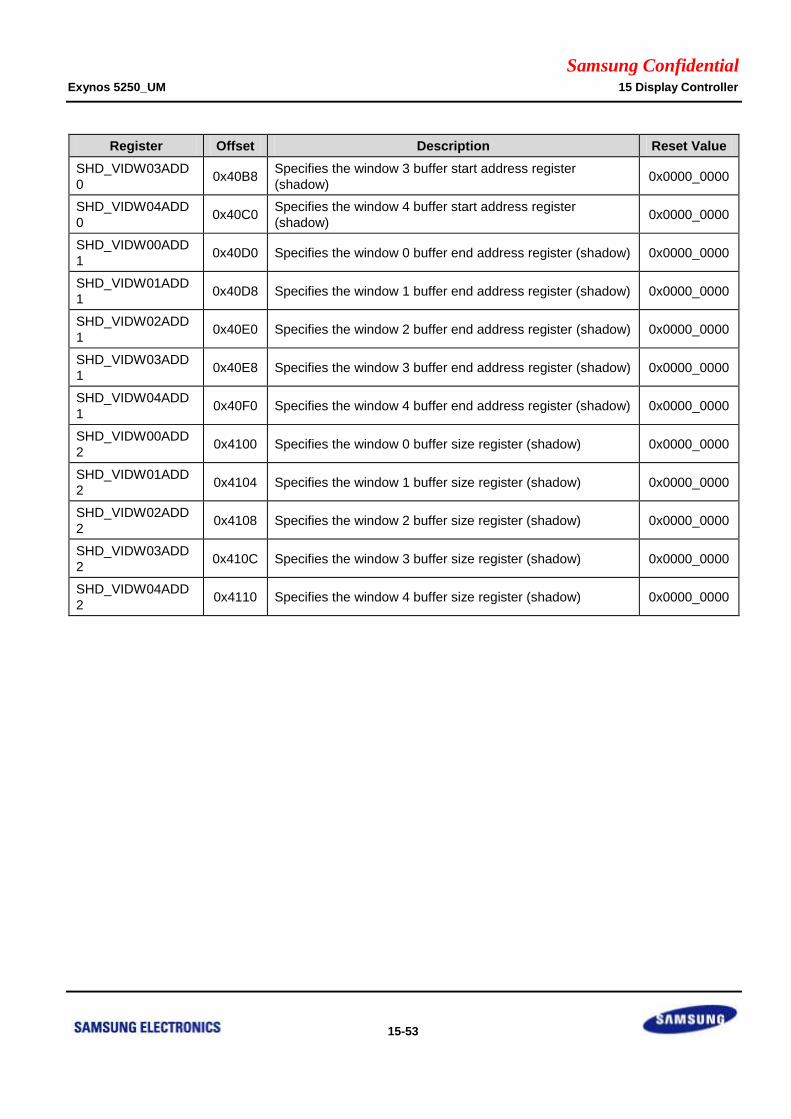
Samsung Confidential Exynos 5250_UM 15 Display Controller
15-53
Register Offset Description Reset Value
SHD_VIDW03ADD
0 0x40B8
Specifies the window 3 buffer start address register
(shadow) 0x0000_0000
SHD_VIDW04ADD
0 0x40C0
Specifies the window 4 buffer start address register
(shadow) 0x0000_0000
SHD_VIDW00ADD
1 0x40D0 Specifies the window 0 buffer end address register (shadow) 0x0000_0000
SHD_VIDW01ADD
1 0x40D8 Specifies the window 1 buffer end address register (shadow) 0x0000_0000
SHD_VIDW02ADD
1 0x40E0 Specifies the window 2 buffer end address register (shadow) 0x0000_0000
SHD_VIDW03ADD
1 0x40E8 Specifies the window 3 buffer end address register (shadow) 0x0000_0000
SHD_VIDW04ADD
1 0x40F0 Specifies the window 4 buffer end address register (shadow) 0x0000_0000
SHD_VIDW00ADD
2 0x4100 Specifies the window 0 buffer size register (shadow) 0x0000_0000
SHD_VIDW01ADD
2 0x4104 Specifies the window 1 buffer size register (shadow) 0x0000_0000
SHD_VIDW02ADD
2 0x4108 Specifies the window 2 buffer size register (shadow) 0x0000_0000
SHD_VIDW03ADD
2 0x410C Specifies the window 3 buffer size register (shadow) 0x0000_0000
SHD_VIDW04ADD
2 0x4110 Specifies the window 4 buffer size register (shadow) 0x0000_0000
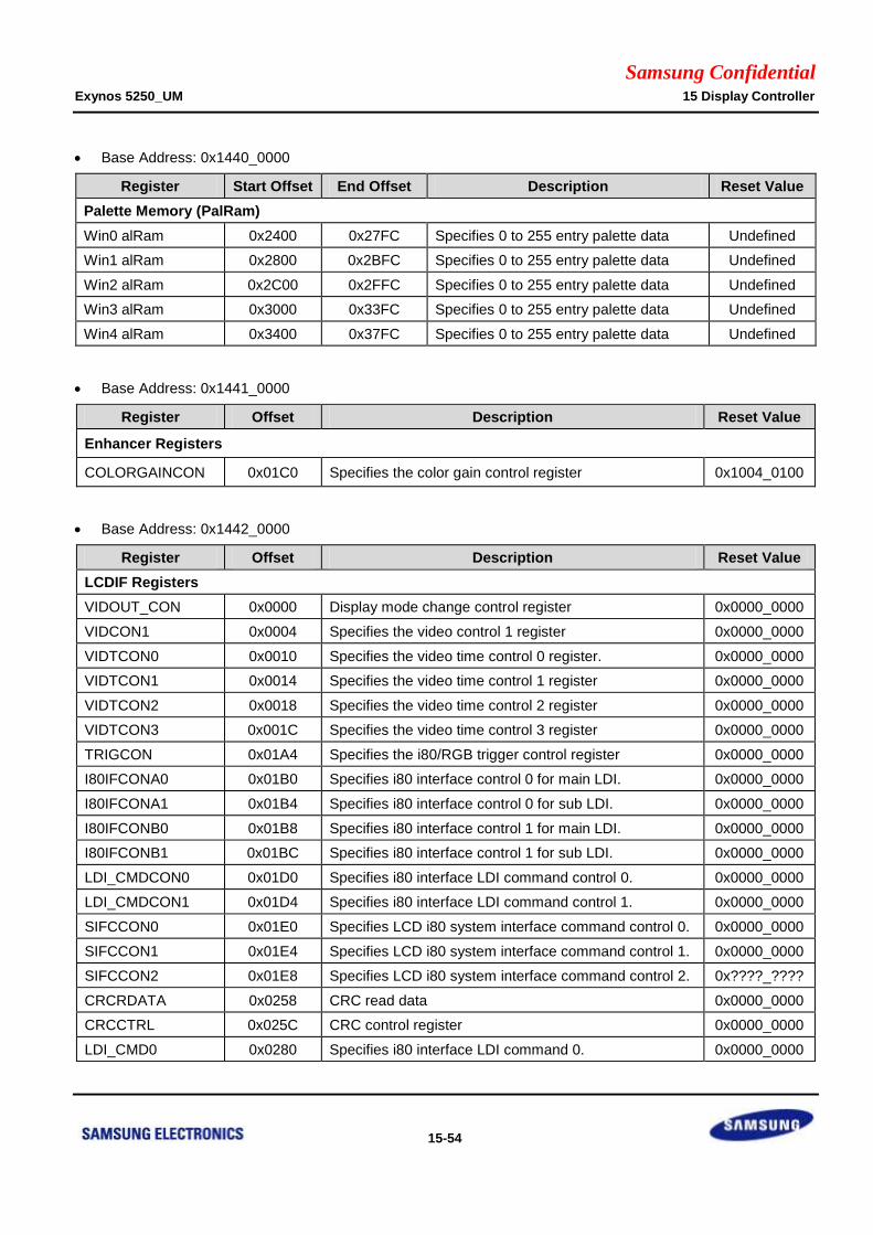
Samsung Confidential Exynos 5250_UM 15 Display Controller
15-54
Base Address: 0x1440_0000
Register Start Offset End Offset Description Reset Value
Palette Memory (PalRam)
Win0 alRam 0x2400 0x27FC Specifies 0 to 255 entry palette data Undefined
Win1 alRam 0x2800 0x2BFC Specifies 0 to 255 entry palette data Undefined
Win2 alRam 0x2C00 0x2FFC Specifies 0 to 255 entry palette data Undefined
Win3 alRam 0x3000 0x33FC Specifies 0 to 255 entry palette data Undefined
Win4 alRam 0x3400 0x37FC Specifies 0 to 255 entry palette data Undefined
Base Address: 0x1441_0000
Register Offset Description Reset Value
Enhancer Registers
COLORGAINCON 0x01C0 Specifies the color gain control register 0x1004_0100
Base Address: 0x1442_0000
Register Offset Description Reset Value
LCDIF Registers
VIDOUT_CON 0x0000 Display mode change control register 0x0000_0000
VIDCON1 0x0004 Specifies the video control 1 register 0x0000_0000
VIDTCON0 0x0010 Specifies the video time control 0 register. 0x0000_0000
VIDTCON1 0x0014 Specifies the video time control 1 register 0x0000_0000
VIDTCON2 0x0018 Specifies the video time control 2 register 0x0000_0000
VIDTCON3 0x001C Specifies the video time control 3 register 0x0000_0000
TRIGCON 0x01A4 Specifies the i80/RGB trigger control register 0x0000_0000
I80IFCONA0 0x01B0 Specifies i80 interface control 0 for main LDI. 0x0000_0000
I80IFCONA1 0x01B4 Specifies i80 interface control 0 for sub LDI. 0x0000_0000
I80IFCONB0 0x01B8 Specifies i80 interface control 1 for main LDI. 0x0000_0000
I80IFCONB1 0x01BC Specifies i80 interface control 1 for sub LDI. 0x0000_0000
LDI_CMDCON0 0x01D0 Specifies i80 interface LDI command control 0. 0x0000_0000
LDI_CMDCON1 0x01D4 Specifies i80 interface LDI command control 1. 0x0000_0000
SIFCCON0 0x01E0 Specifies LCD i80 system interface command control 0. 0x0000_0000
SIFCCON1 0x01E4 Specifies LCD i80 system interface command control 1. 0x0000_0000
SIFCCON2 0x01E8 Specifies LCD i80 system interface command control 2. 0x????_????
CRCRDATA 0x0258 CRC read data 0x0000_0000
CRCCTRL 0x025C CRC control register 0x0000_0000
LDI_CMD0 0x0280 Specifies i80 interface LDI command 0. 0x0000_0000
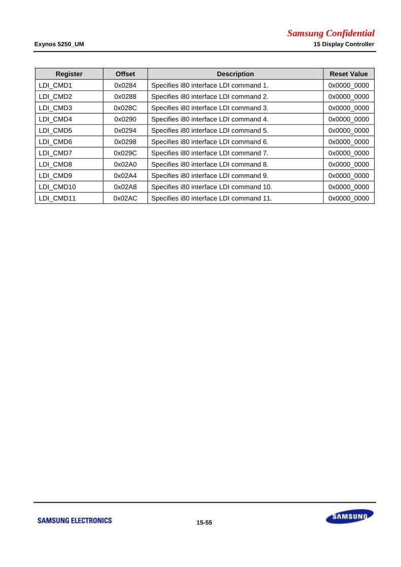
Samsung Confidential Exynos 5250_UM 15 Display Controller
15-55
Register Offset Description Reset Value
LDI_CMD1 0x0284 Specifies i80 interface LDI command 1. 0x0000_0000
LDI_CMD2 0x0288 Specifies i80 interface LDI command 2. 0x0000_0000
LDI_CMD3 0x028C Specifies i80 interface LDI command 3. 0x0000_0000
LDI_CMD4 0x0290 Specifies i80 interface LDI command 4. 0x0000_0000
LDI_CMD5 0x0294 Specifies i80 interface LDI command 5. 0x0000_0000
LDI_CMD6 0x0298 Specifies i80 interface LDI command 6. 0x0000_0000
LDI_CMD7 0x029C Specifies i80 interface LDI command 7. 0x0000_0000
LDI_CMD8 0x02A0 Specifies i80 interface LDI command 8. 0x0000_0000
LDI_CMD9 0x02A4 Specifies i80 interface LDI command 9. 0x0000_0000
LDI_CMD10 0x02A8 Specifies i80 interface LDI command 10. 0x0000_0000
LDI_CMD11 0x02AC Specifies i80 interface LDI command 11. 0x0000_0000
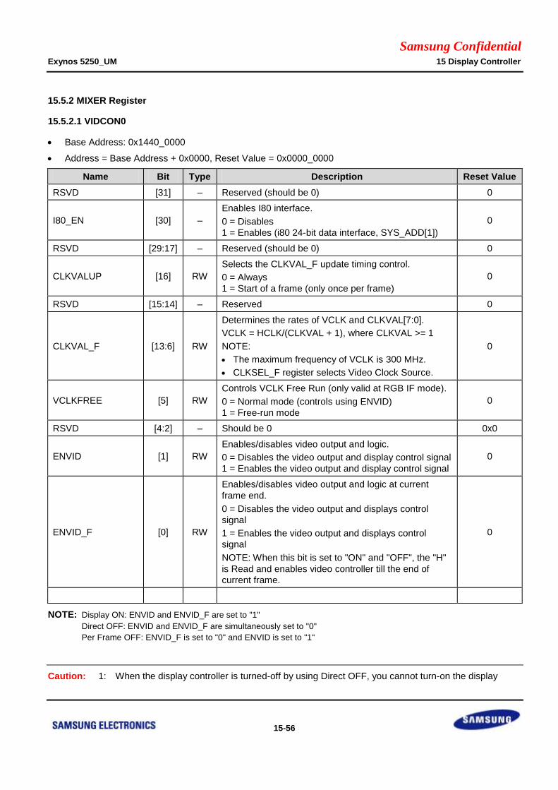
Samsung Confidential Exynos 5250_UM 15 Display Controller
15-56
15.5.2 MIXER Register
15.5.2.1 VIDCON0
Base Address: 0x1440_0000
Address = Base Address + 0x0000, Reset Value = 0x0000_0000
Name Bit Type Description Reset Value
RSVD [31] – Reserved (should be 0) 0
I80_EN [30] –
Enables I80 interface.
0 = Disables
1 = Enables (i80 24-bit data interface, SYS_ADD[1])
0
RSVD [29:17] – Reserved (should be 0) 0
CLKVALUP [16] RW
Selects the CLKVAL_F update timing control.
0 = Always
1 = Start of a frame (only once per frame)
0
RSVD [15:14] – Reserved 0
CLKVAL_F [13:6] RW
Determines the rates of VCLK and CLKVAL[7:0].
VCLK = HCLK/(CLKVAL + 1), where CLKVAL >= 1
NOTE:
The maximum frequency of VCLK is 300 MHz.
CLKSEL_F register selects Video Clock Source.
0
VCLKFREE [5] RW
Controls VCLK Free Run (only valid at RGB IF mode).
0 = Normal mode (controls using ENVID)
1 = Free-run mode
0
RSVD [4:2] – Should be 0 0x0
ENVID [1] RW
Enables/disables video output and logic.
0 = Disables the video output and display control signal
1 = Enables the video output and display control signal
0
ENVID_F [0] RW
Enables/disables video output and logic at current
frame end.
0 = Disables the video output and displays control
signal
1 = Enables the video output and displays control
signal
NOTE: When this bit is set to "ON" and "OFF", the "H"
is Read and enables video controller till the end of
current frame.
0
NOTE: Display ON: ENVID and ENVID_F are set to "1"
Direct OFF: ENVID and ENVID_F are simultaneously set to "0"
Per Frame OFF: ENVID_F is set to "0" and ENVID is set to "1"
Caution: 1: When the display controller is turned-off by using Direct OFF, you cannot turn-on the display
Samsung Confidential Exynos 5250_UM 15 Display Controller
15-57
controller without a reset.
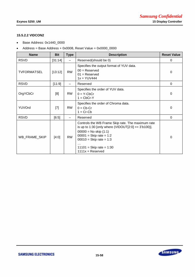
Samsung Confidential Exynos 5250_UM 15 Display Controller
15-58
15.5.2.2 VIDCON2
Base Address: 0x1440_0000
Address = Base Address + 0x0008, Reset Value = 0x0000_0000
Name Bit Type Description Reset Value
RSVD [31:14] – Reserved(should be 0) 0
TVFORMATSEL [13:12] RW
Specifies the output format of YUV data.
00 = Reserved
01 = Reserved
1x = YUV444
0
RSVD [11:9] – Reserved 0
OrgYCbCr [8] RW
Specifies the order of YUV data.
0 = Y-CbCr
1 = CbCr-Y
0
YUVOrd [7] RW
Specifies the order of Chroma data.
0 = Cb-Cr
1 = Cr-Cb
0
RSVD [6:5] – Reserved 0
WB_FRAME_SKIP [4:0] RW
Controls the WB Frame Skip rate. The maximum rate
is up to 1:30 [only where (VIDOUT[2:0] == 3’b100)].
00000 = No skip (1:1)
00001 = Skip rate = 1:2
00010 = Skip rate = 1:3
…
11101 = Skip rate = 1:30
1111x = Reserved
0
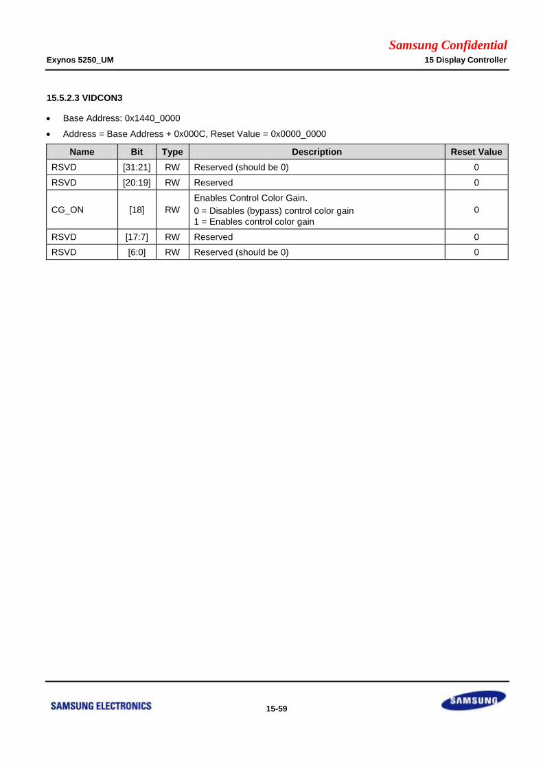
Samsung Confidential Exynos 5250_UM 15 Display Controller
15-59
15.5.2.3 VIDCON3
Base Address: 0x1440_0000
Address = Base Address + 0x000C, Reset Value = 0x0000_0000
Name Bit Type Description Reset Value
RSVD [31:21] RW Reserved (should be 0) 0
RSVD [20:19] RW Reserved 0
CG_ON [18] RW
Enables Control Color Gain.
0 = Disables (bypass) control color gain
1 = Enables control color gain
0
RSVD [17:7] RW Reserved 0
RSVD [6:0] RW Reserved (should be 0) 0
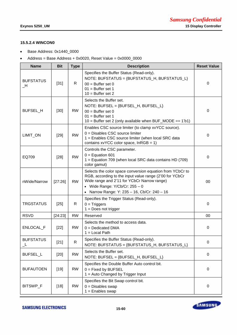
Samsung Confidential Exynos 5250_UM 15 Display Controller
15-60
15.5.2.4 WINCON0
Base Address: 0x1440_0000
Address = Base Address + 0x0020, Reset Value = 0x0000_0000
Name Bit Type Description Reset Value
BUFSTATUS
_H [31] R
Specifies the Buffer Status (Read-only).
NOTE: BUFSTATUS = {BUFSTATUS_H, BUFSTATUS_L}
00 = Buffer set 0
01 = Buffer set 1
10 = Buffer set 2
0
BUFSEL_H [30] RW
Selects the Buffer set.
NOTE: BUFSEL = {BUFSEL_H, BUFSEL_L}
00 = Buffer set 0
01 = Buffer set 1
10 = Buffer set 2 (only available when BUF_MODE == 1’b1)
0
LIMIT_ON [29] RW
Enables CSC source limiter (to clamp xvYCC source).
0 = Disables CSC source limiter
1 = Enables CSC source limiter (when local SRC data
contains xvYCC color space, InRGB = 1)
0
EQ709 [28] RW
Controls the CSC parameter.
0 = Equation 601
1 = Equation 709 (when local SRC data contains HD (709)
color gamut)
0
nWide/Narrow [27:26] RW
Selects the color space conversion equation from YCbCr to
RGB, according to the input value range (2’00 for YCbCr
Wide range and 2’11 for YCbCr Narrow range)
Wide Range: Y/Cb/Cr: 255 – 0
Narrow Range: Y: 235 – 16, Cb/Cr: 240 – 16
00
TRGSTATUS [25] R
Specifies the Trigger Status (Read-only).
0 = Triggers
1 = Does not trigger
0
RSVD [24:23] RW Reserved 00
ENLOCAL_F [22] RW
Selects the method to access data.
0 = Dedicated DMA
1 = Local Path
0
BUFSTATUS
_L [21] R
Specifies the Buffer Status (Read-only).
NOTE: BUFSTATUS = {BUFSTATUS_H, BUFSTATUS_L} 0
BUFSEL_L [20] RW Selects the Buffer set.
NOTE: BUFSEL = {BUFSEL_H, BUFSEL_L} 0
BUFAUTOEN [19] RW
Specifies the Double Buffer Auto control bit.
0 = Fixed by BUFSEL
1 = Auto Changed by Trigger Input
0
BITSWP_F [18] RW
Specifies the Bit Swap control bit.
0 = Disables swap
1 = Enables swap
0
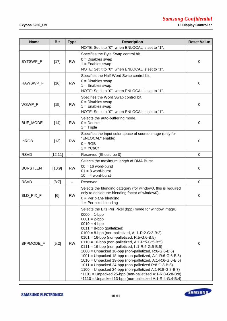
Samsung Confidential Exynos 5250_UM 15 Display Controller
15-61
Name Bit Type Description Reset Value
NOTE: Set it to "0", when ENLOCAL is set to "1".
BYTSWP_F [17] RW
Specifies the Byte Swap control bit.
0 = Disables swap
1 = Enables swap
NOTE: Set it to "0", when ENLOCAL is set to "1".
0
HAWSWP_F [16] RW
Specifies the Half-Word Swap control bit.
0 = Disables swap
1 = Enables swap
NOTE: Set it to "0", when ENLOCAL is set to "1".
0
WSWP_F [15] RW
Specifies the Word Swap control bit.
0 = Disables swap
1 = Enables swap
NOTE: Set it to "0", when ENLOCAL is set to "1".
0
BUF_MODE [14] RW
Selects the auto-buffering mode.
0 = Double
1 = Triple
0
InRGB [13] RW
Specifies the input color space of source image (only for
"ENLOCAL" enable).
0 = RGB
1 = YCbCr
0
RSVD [12:11] – Reserved (Should be 0) 0
BURSTLEN [10:9] RW
Selects the maximum length of DMA Burst.
00 = 16 word-burst
01 = 8 word-burst
10 = 4 word-burst
0
RSVD [8:7] – Reserved 0
BLD_PIX_F [6] RW
Selects the blending category (for window0, this is required
only to decide the blending factor of window0).
0 = Per plane blending
1 = Per pixel blending
0
BPPMODE_F [5:2] RW
Selects the Bits Per Pixel (bpp) mode for window image.
0000 = 1-bpp
0001 = 2-bpp
0010 = 4-bpp
0011 = 8-bpp (palletized)
0100 = 8-bpp (non-palletized, A: 1-R:2-G:3-B:2)
0101 = 16-bpp (non-palletized, R:5-G:6-B:5)
0110 = 16-bpp (non-palletized, A:1-R:5-G:5-B:5)
0111 = 16-bpp (non-palletized, I :1-R:5-G:5-B:5)
1000 = Unpacked 18-bpp (non-palletized, R:6-G:6-B:6)
1001 = Unpacked 18-bpp (non-palletized, A:1-R:6-G:6-B:5)
1010 = Unpacked 19-bpp (non-palletized, A:1-R:6-G:6-B:6)
1011 = Unpacked 24-bpp (non-palletized R:8-G:8-B:8)
1100 = Unpacked 24-bpp (non-palletized A:1-R:8-G:8-B:7)
*1101 = Unpacked 25-bpp (non-palletized A:1-R:8-G:8-B:8)
*1110 = Unpacked 13-bpp (non-palletized A:1-R:4-G:4-B:4)
0
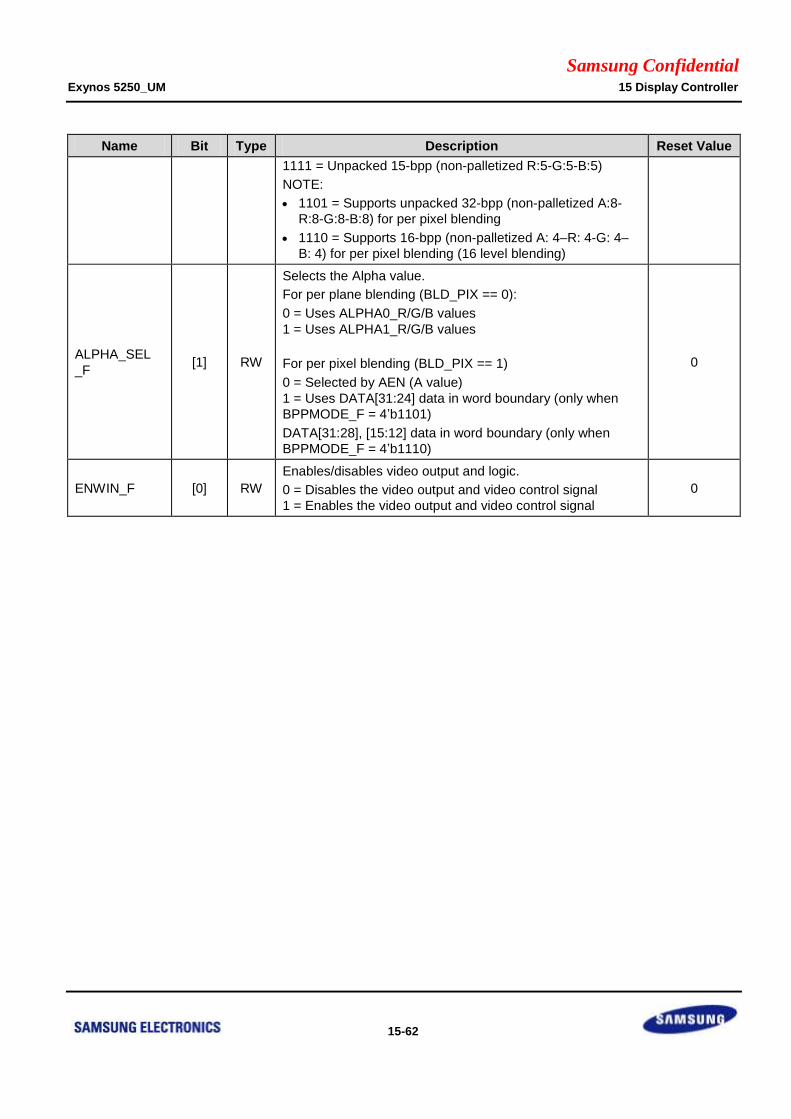
Samsung Confidential Exynos 5250_UM 15 Display Controller
15-62
Name Bit Type Description Reset Value
1111 = Unpacked 15-bpp (non-palletized R:5-G:5-B:5)
NOTE:
1101 = Supports unpacked 32-bpp (non-palletized A:8-
R:8-G:8-B:8) for per pixel blending
1110 = Supports 16-bpp (non-palletized A: 4–R: 4-G: 4–
B: 4) for per pixel blending (16 level blending)
ALPHA_SEL
_F [1] RW
Selects the Alpha value.
For per plane blending (BLD_PIX == 0):
0 = Uses ALPHA0_R/G/B values
1 = Uses ALPHA1_R/G/B values
For per pixel blending (BLD_PIX == 1)
0 = Selected by AEN (A value)
1 = Uses DATA[31:24] data in word boundary (only when
BPPMODE_F = 4’b1101)
DATA[31:28], [15:12] data in word boundary (only when
BPPMODE_F = 4’b1110)
0
ENWIN_F [0] RW
Enables/disables video output and logic.
0 = Disables the video output and video control signal
1 = Enables the video output and video control signal
0
Samsung Confidential Exynos 5250_UM 15 Display Controller
15-63
15.5.2.5 WINCON1
Base Address: 0x1440_0000
Address = Base Address + 0x0024, Reset Value = 0x0000_0000
Name Bit Type Description Reset Value
BUFSTATUS
_H [31] R
Specifies the Buffer Status (Read-only).
NOTE: BUFSTATUS = {BUFSTATUS_H, BUFSTATUS_L}
00 = Buffer set 0
01 = Buffer set 1
10 = Buffer set 2
0
BUFSEL_H [30] RW
Selects the Buffer set.
NOTE: BUFSEL = {BUFSEL_H, BUFSEL_L}
00 = Buffer set 0
01 = Buffer set 1
10 = Buffer set 2 (available only when BUF_MODE == 1’b1)
0
LIMIT_ON [29] RW
Enables Control CSC source limiter (to clamp xvYCC
source).
0 = Disables control CSC source limiter
1 = Enables control CSC source limiter (when local SRC
data contains xvYCC color space, InRGB = 1)
0
EQ709 [28] RW
Controls the CSC parameter.
0 = Equation 601
1 = Equation 709 (when local SRC data has HD (709) color
gamut)
0
nWide/Narrow [27:26] RW
Selects the color space conversion equation from YCbCr to
RGB, based on the input value range (2’00 for YCbCr Wide
range and 2’11 for YCbCr Narrow range).
Wide Range: Y/Cb/Cr: 255 – 0
Narrow Range: Y: 235 – 16, Cb/Cr: 240 – 16
00
TRGSTATUS [25] R
Specifies the Window 1 Software Trigger Update Status
(Read-only).
0 = Updates
1 = Does not update
When the Software Trigger in window 1 occurs, this bit is
automatically set to "1". This value clears only after updating
the shadow register sets.
0
RSVD [24:23] – Reserved (should be 0) 0
ENLOCAL_F [22] RW
Selects the method to access data.
0 = Dedicated DMA
1 = Local Path
0
BUFSTATUS
_L [21] R
Specifies the Buffer Status (Read-only).
NOTE: BUFSTATUS = {BUFSTATUS_H, BUFSTATUS_L} 0
BUFSEL_L [20] RW Selects the Buffer set.
NOTE: BUFSEL = {BUFSEL_H, BUFSEL_L} 0
BUFAUTOEN [19] RW Specifies the Double Buffer Auto control bit. 0
Samsung Confidential Exynos 5250_UM 15 Display Controller
15-64
Name Bit Type Description Reset Value
0 = Fixed by BUFSEL
1 = Auto changed by Trigger Input
BITSWP_F [18] RW
Specifies the Bit Swap control bit.
0 = Disables swap
1 = Enables swap
NOTE: Set it to "0", when ENLOCAL is set to "1".
0
BYTSWP_F [17] RW
Specifies the Byte Swap control bit.
0 = Disables swap
1 = Enables swapo
NOTE: Set it to "0", when ENLOCAL is set to "1".
0
HAWSWP_F [16] RW
Specifies the Half-Word Swap control bit.
0 = Disables swap
1 = Enables swap
NOTE: Set it to "0", when ENLOCAL is set to "1".
0
WSWP_F [15] RW
Specifies the Word Swap control bit.
0 = Disables swap
1 = Enables swap
NOTE: Set it to "0", when ENLOCAL is set to "1".
0
BUF_MODE [14] RW
Selects the Auto-buffering mode.
0 = Double
1 = Triple
0
InRGB [13] RW
Indicates the input color space of source image (applicable
only for "EnLcal" enable).
0 = RGB
1 = YCbCr
0
RSVD [12:11] – Reserved (should be 0) 0
BURSTLEN [10:9] RW
Specifies the maximum length selection of DMA Burst.
00 = 16 word-burst
01 = 8 word-burst
10 = 4 word-burst
0
RSVD [8] – Reserved (should be 0) 0
ALPHA_MUL
_F [7] RW
Specifies the Multiplied Alpha value mode.
0 = Disables multiplied mode
1 = Enables multiplied mode
When ALPHA_MUL is set to "1", set BLD_PIX = 1,
ALPHA_SEL = 1, and BPPMODE_F[5:2] = 4’b1101 or
4’b1110.
NOTE: Alpha value = alpha_pixel (from data)
ALPHA0_R/G/B
0
BLD_PIX_F [6] RW
Selects the blending category.
0 = Per plane blending
1 = Per pixel blending
0
BPPMODE_F [5:2] RW Selects the Bits Per Pixel (bpp) mode in Window image.
0000 = 1-bpp 0
Samsung Confidential Exynos 5250_UM 15 Display Controller
15-65
Name Bit Type Description Reset Value
0001 = 2-bpp
0010 = 4-bpp
0011 = 8-bpp (palletized)
0100 = 8-bpp (non-palletized, A: 1-R:2-G:3-B:2)
0101 = 16-bpp (non-palletized, R: 5-G: 6-B:5)
0110 = 16-bpp (non-palletized, A:1-R:5-G:5-B:5)
0111 = 16-bpp (non-palletized, I :1-R:5-G:5-B:5)
1000 = Unpacked 18-bpp (non-palletized, R:6-G:6-B:6)
1001 = Unpacked 18-bpp (non-palletized, A:1-R:6-G:6-B:5)
1010 = Unpacked 19-bpp (non-palletized, A:1-R:6-G:6-B:6)
1011 = Unpacked 24-bpp (non-palletized R:8-G:8-B:8)
1100 = Unpacked 24-bpp (non-palletized A:1-R:8-G:8-B:7)
*1101 = Unpacked 25-bpp (non-palletized A:1-R:8-G:8-B:8)
*1110 = Unpacked 13-bpp (non-palletized A:1-R:4-G:4-B:4)
1111 = Unpacked 15-bpp (non-palletized R:5-G:5-B:5)
NOTE:
1101 = supports unpacked 32-bpp (non-palletized A:8-
R:8-G:8-B:8) for per pixel blending
1110 = supports 16-bpp (non-palletized A:4-R:4-G:4-B:4)
for per pixel blending. (16 level blending)
ALPHA_SEL
_F [1] RW
Selects the Alpha value.
For per plane blending (BLD_PIX == 0)
0 = Uses ALPHA0_R/G/B values
1 = Uses ALPHA1_R/G/B values
For per pixel blending (BLD_PIX == 1)
0 = Selected by AEN (A value)
1 = Uses DATA[31:24] data in word boundary (only when
BPPMODE_F = 4’b1101)
DATA[31:28], [15:12] data in word boundary (only when
BPPMODE_F = 4’b1110)
0
ENWIN_F [0] RW
Enables/disables video output and logic.
0 = Disables the video output and video control signal
1 = Enables the video output and video control signal
0

Samsung Confidential Exynos 5250_UM 15 Display Controller
15-66
15.5.2.6 WINCON2
Base Address: 0x1440_0000
Address = Base Address + 0x0028, Reset Value = 0x0000_0000
Name Bit Type Description Reset Value
BUFSTATUS
_H [31] R
Specifies the Buffer Status (Read-only).
NOTE: BUFSTATUS = {BUFSTATUS_H, BUFSTATUS_L}
00 = Buffer set 0
01 = Buffer set 1
10 = Buffer set 2
0
BUFSEL_H [30] RW
Selects the Buffer set.
00 = Buffer set 0
01 = Buffer set 1
10 = Buffer set 2 (available only when BUF_MODE == 1’b1)
NOTE: BUFSEL = {BUFSEL_H, BUFSEL_L}
0
LIMIT_ON [29] RW
Enables CSC source limiter (for clamping xvYCC source).
0 = Disables CSC source limiter
1 = Enables CSC source limiter (when local SRC data
contains xvYCC color space, InRGB = 1)
0
EQ709 [28] RW
Controls CSC parameter.
0 = Equation 601
1 = Equation 709 (when local SRC data has HD (709) color
gamut)
0
nWide/Narrow [27:26] RW
Selects color space conversion equation from YCbCr to
RGB, based on the input value range (2’00 for YCbCr Wide
range and 2’11 for YCbCr Narrow range).
Wide Range: Y/Cb/Cr: 255 – 0
Narrow Range: Y: 235 – 16, Cb/Cr: 240 – 16
00
RSVD [25:24] – Reserved 00
LOCALSEL_F [23] RW
Selects the local path source.
0 = Local Path2
1 = Local Path3
0
ENLOCAL_F [22] RW
Selects the method to access data.
0 = Dedicated DMA
1 = Local Path
0
BUFSTATUS
_L [21] R
Specifies the Buffer Status (Read-only).
NOTE: BUFSTATUS = {BUFSTATUS_H, BUFSTATUS_L}
BUFSEL_L [20] RW Selects the Buffer set.
NOTE: BUFSEL = {BUFSEL_H, BUFSEL_L} 0
BUFAUTOEN [19] RW
Specifies the Double Buffer Auto control bit.
0 = Fixed by BUFSEL
1 = Auto changed by Trigger Input
0
BITSWP_F [18] RW
Specifies the Bit Swap control bit.
0 = Disables swap
1 = Enables swap
0
Samsung Confidential Exynos 5250_UM 15 Display Controller
15-67
Name Bit Type Description Reset Value
NOTE: Set it to "0", when ENLOCAL is set to "1".
BYTSWP_F [17] RW
Specifies the Byte Swap control bit.
0 = Disables swap
1 = Enables swap
NOTE: Set it to "0", when ENLOCAL is set to "1".
0
HAWSWP_F [16] RW
Specifies the Half-Word Swap control bit.
0 = Disables swap
1 = Enables swap
NOTE: Set it to "0", when ENLOCAL is set to "1".
0
WSWP_F [15] RW
Specifies the Word Swap control bit.
0 = Disables swap
1 = Enables swap
NOTE: It should be 0 when ENLOCAL is 1.
0
BUF_MODE [14] RW
Selects the auto-buffering mode.
0 = Double
1 = Triple
0
InRGB [13] RW
Specifies the input color space of source image (applicable
only for "EnLcal" enable).
0 = RGB
1 = YCbCr
0
RSVD [12:11] – Reserved (should be 0) 0
BURSTLEN [10:9] RW
Selects the maximum length of the DMA Burst.
00 = 16 word-burst
01 = 8 word-burst
10 = 4 word-burst
0
RSVD [8] – Reserved (should be 0) 0
ALPHA_MUL
_F [7] RW
Specifies the Multiplied Alpha value mode.
0 = Disables multiple mode
1 = Enables multiplied mode
When ALPHA_MUL is set to "1", set BLD_PIX = 1,
ALPHA_SEL = 1, and BPPMODE_F[5:2] = 4’b1101 or
4’b1110.
NOTE: Alpha value = alpha_pixel (from data)
ALPHA0_R/G/B
0
BLD_PIX_F [6] RW
Selects the blending category.
0 = Per plane blending
1 = Per pixel blending
0
BPPMODE
_F [5:2] RW
Selects the Bits Per Pixel (bpp) mode in Window image.
0000 = 1-bpp
0001 = 2-bpp
0010 = 4-bpp
0011 = 8-bpp (palletized)
0100 = 8-bpp (non-palletized, A: 1-R:2-G:3-B:2)
0101 = 16-bpp (non-palletized, R:5-G:6-B:5)
0110 = 16-bpp (non-palletized, A:1-R:5-G:5-B:5)
0
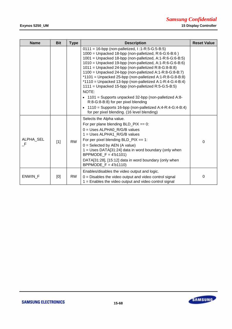
Samsung Confidential Exynos 5250_UM 15 Display Controller
15-68
Name Bit Type Description Reset Value
0111 = 16-bpp (non-palletized, I :1-R:5-G:5-B:5)
1000 = Unpacked 18-bpp (non-palletized, R:6-G:6-B:6 )
1001 = Unpacked 18-bpp (non-palletized, A:1-R:6-G:6-B:5)
1010 = Unpacked 19-bpp (non-palletized, A:1-R:6-G:6-B:6)
1011 = Unpacked 24-bpp (non-palletized R:8-G:8-B:8)
1100 = Unpacked 24-bpp (non-palletized A:1-R:8-G:8-B:7)
*1101 = Unpacked 25-bpp (non-palletized A:1-R:8-G:8-B:8)
*1110 = Unpacked 13-bpp (non-palletized A:1-R:4-G:4-B:4)
1111 = Unpacked 15-bpp (non-palletized R:5-G:5-B:5)
NOTE:
1101 = Supports unpacked 32-bpp (non-palletized A:8-
R:8-G:8-B:8) for per pixel blending
1110 = Supports 16-bpp (non-palletized A:4-R:4-G:4-B:4)
for per pixel blending. (16 level blending)
ALPHA_SEL
_F [1] RW
Selects the Alpha value.
For per plane blending BLD_PIX == 0:
0 = Uses ALPHA0_R/G/B values
1 = Uses ALPHA1_R/G/B values
For per pixel blending BLD_PIX == 1:
0 = Selected by AEN (A value)
1 = Uses DATA[31:24] data in word boundary (only when
BPPMODE_F = 4’b1101)
DATA[31:28], [15:12] data in word boundary (only when
BPPMODE_F = 4’b1110)
0
ENWIN_F [0] RW
Enables/disables the video output and logic.
0 = Disables the video output and video control signal
1 = Enables the video output and video control signal
0
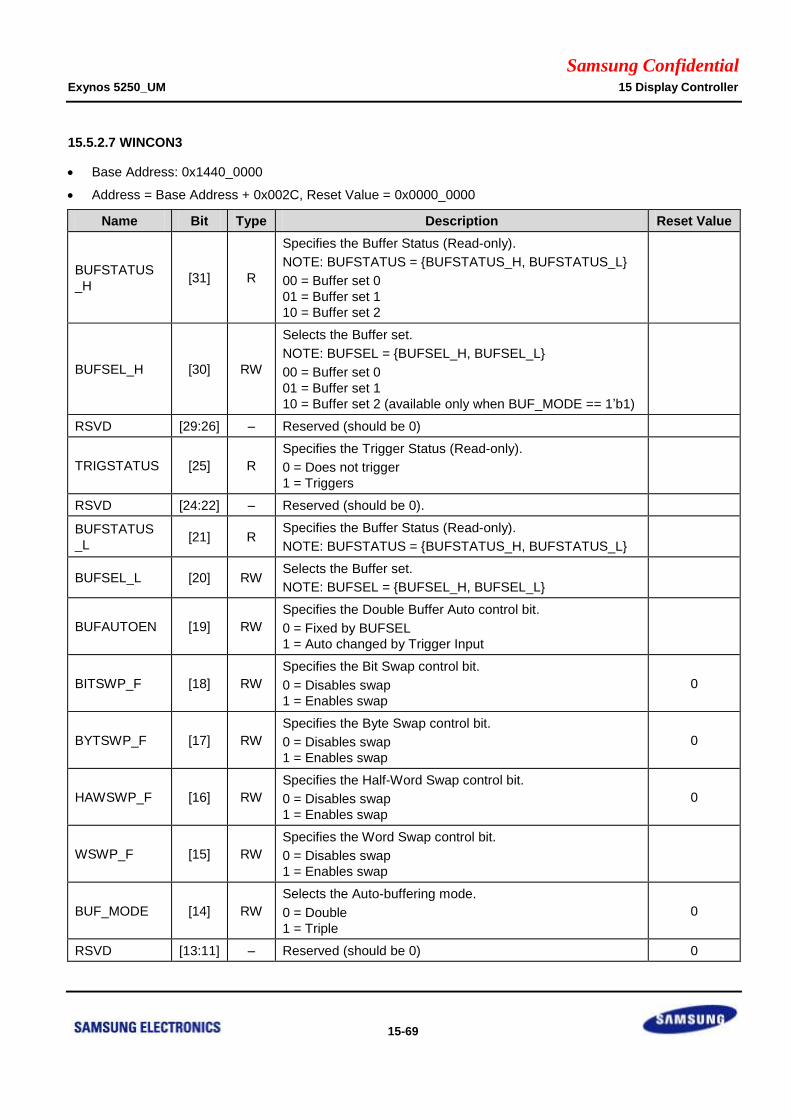
Samsung Confidential Exynos 5250_UM 15 Display Controller
15-69
15.5.2.7 WINCON3
Base Address: 0x1440_0000
Address = Base Address + 0x002C, Reset Value = 0x0000_0000
Name Bit Type Description Reset Value
BUFSTATUS
_H [31] R
Specifies the Buffer Status (Read-only).
NOTE: BUFSTATUS = {BUFSTATUS_H, BUFSTATUS_L}
00 = Buffer set 0
01 = Buffer set 1
10 = Buffer set 2
BUFSEL_H [30] RW
Selects the Buffer set.
NOTE: BUFSEL = {BUFSEL_H, BUFSEL_L}
00 = Buffer set 0
01 = Buffer set 1
10 = Buffer set 2 (available only when BUF_MODE == 1’b1)
RSVD [29:26] – Reserved (should be 0)
TRIGSTATUS [25] R
Specifies the Trigger Status (Read-only).
0 = Does not trigger
1 = Triggers
RSVD [24:22] – Reserved (should be 0).
BUFSTATUS
_L [21] R
Specifies the Buffer Status (Read-only).
NOTE: BUFSTATUS = {BUFSTATUS_H, BUFSTATUS_L}
BUFSEL_L [20] RW Selects the Buffer set.
NOTE: BUFSEL = {BUFSEL_H, BUFSEL_L}
BUFAUTOEN [19] RW
Specifies the Double Buffer Auto control bit.
0 = Fixed by BUFSEL
1 = Auto changed by Trigger Input
BITSWP_F [18] RW
Specifies the Bit Swap control bit.
0 = Disables swap
1 = Enables swap
0
BYTSWP_F [17] RW
Specifies the Byte Swap control bit.
0 = Disables swap
1 = Enables swap
0
HAWSWP_F [16] RW
Specifies the Half-Word Swap control bit.
0 = Disables swap
1 = Enables swap
0
WSWP_F [15] RW
Specifies the Word Swap control bit.
0 = Disables swap
1 = Enables swap
BUF_MODE [14] RW
Selects the Auto-buffering mode.
0 = Double
1 = Triple
0
RSVD [13:11] – Reserved (should be 0) 0
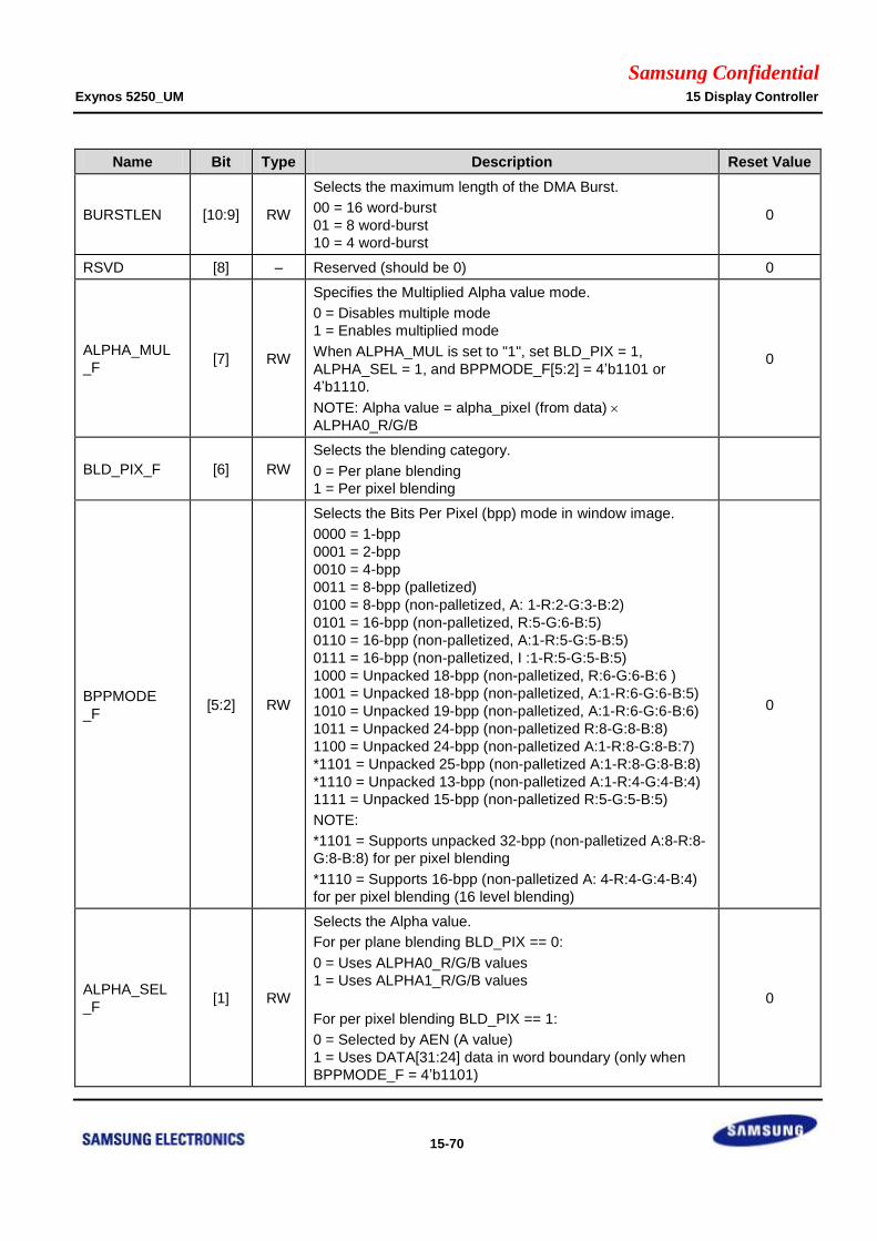
Samsung Confidential Exynos 5250_UM 15 Display Controller
15-70
Name Bit Type Description Reset Value
BURSTLEN [10:9] RW
Selects the maximum length of the DMA Burst.
00 = 16 word-burst
01 = 8 word-burst
10 = 4 word-burst
0
RSVD [8] – Reserved (should be 0) 0
ALPHA_MUL
_F [7] RW
Specifies the Multiplied Alpha value mode.
0 = Disables multiple mode
1 = Enables multiplied mode
When ALPHA_MUL is set to "1", set BLD_PIX = 1,
ALPHA_SEL = 1, and BPPMODE_F[5:2] = 4’b1101 or
4’b1110.
NOTE: Alpha value = alpha_pixel (from data)
ALPHA0_R/G/B
0
BLD_PIX_F [6] RW
Selects the blending category.
0 = Per plane blending
1 = Per pixel blending
BPPMODE
_F [5:2] RW
Selects the Bits Per Pixel (bpp) mode in window image.
0000 = 1-bpp
0001 = 2-bpp
0010 = 4-bpp
0011 = 8-bpp (palletized)
0100 = 8-bpp (non-palletized, A: 1-R:2-G:3-B:2)
0101 = 16-bpp (non-palletized, R:5-G:6-B:5)
0110 = 16-bpp (non-palletized, A:1-R:5-G:5-B:5)
0111 = 16-bpp (non-palletized, I :1-R:5-G:5-B:5)
1000 = Unpacked 18-bpp (non-palletized, R:6-G:6-B:6 )
1001 = Unpacked 18-bpp (non-palletized, A:1-R:6-G:6-B:5)
1010 = Unpacked 19-bpp (non-palletized, A:1-R:6-G:6-B:6)
1011 = Unpacked 24-bpp (non-palletized R:8-G:8-B:8)
1100 = Unpacked 24-bpp (non-palletized A:1-R:8-G:8-B:7)
*1101 = Unpacked 25-bpp (non-palletized A:1-R:8-G:8-B:8)
*1110 = Unpacked 13-bpp (non-palletized A:1-R:4-G:4-B:4)
1111 = Unpacked 15-bpp (non-palletized R:5-G:5-B:5)
NOTE:
*1101 = Supports unpacked 32-bpp (non-palletized A:8-R:8-
G:8-B:8) for per pixel blending
*1110 = Supports 16-bpp (non-palletized A: 4-R:4-G:4-B:4)
for per pixel blending (16 level blending)
0
ALPHA_SEL
_F [1] RW
Selects the Alpha value.
For per plane blending BLD_PIX == 0:
0 = Uses ALPHA0_R/G/B values
1 = Uses ALPHA1_R/G/B values
For per pixel blending BLD_PIX == 1:
0 = Selected by AEN (A value)
1 = Uses DATA[31:24] data in word boundary (only when
BPPMODE_F = 4’b1101)
0

Samsung Confidential Exynos 5250_UM 15 Display Controller
15-71
Name Bit Type Description Reset Value
DATA[31:28], [15:12] data in word boundary (only when
BPPMODE_F = 4’b1110)
ENWIN_F [0] RW
Enables/disables video output and logic.
0 = Disables the video output and video control signal
1 = Enables the video output and video control signal
0

Samsung Confidential Exynos 5250_UM 15 Display Controller
15-72
15.5.2.8 WINCON4
Base Address: 0x1440_0000
Address = Base Address + 0x0030, Reset Value = 0x0000_0000
Name Bit Type Description Reset Value
BUFSTATUS
_H [31] R
Specifies the Buffer Status (Read-only).
NOTE: BUFSTATUS = {BUFSTATUS_H, BUFSTATUS_L}
00 = Buffer set 0
01 = Buffer set 1
10 = Buffer set 2
0
BUFSEL_H [30] RW
Selects the Buffer set.
NOTE: BUFSEL = {BUFSEL_H, BUFSEL_L}
00 = Buffer set 0
01 = Buffer set 1
10 = Buffer set 2 (only available where BUF_MODE == 1’b1)
0
RSVD [29:26] – Reserved (should be 0) 0
TRIGSTATUS [25] R
Specifies the Trigger Status (Read-only).
0 = Does not trigger
1 = Triggers
0
RSVD [24:22] – Reserved (should be 0) 0
BUFSTATUS
_L [21] R
Specifies the Buffer Status (Read-only).
NOTE: BUFSTATUS = {BUFSTATUS_H, BUFSTATUS_L} 0
BUFSEL_L [20] RW Selects the Buffer set.
NOTE: BUFSEL = {BUFSEL_H, BUFSEL_L} 0
BUFAUTOEN [19] RW
Specifies the Double Buffer Auto control bit.
0 = Fixed by BUFSEL
1 = Auto changed by Trigger Input
0
BITSWP_F [18] RW
Specifies the Bit Swap control bit.
0 = Disables swap
1 = Enables swap
0
BYTSWP_F [17] RW
Specifies the Byte Swap control bit.
0 = Disables swap
1 = Enables swap
0
HAWSWP_F [16] RW
Specifies the Half-Word Swap control bit.
0 = Disables swap
1 = Enables swap
0
WSWP_F [15] RW
Specifies the Word Swap control bit.
0 = Disables swap
1 = Enables swap
0
BUF_MODE [14] RW
Selects the Auto-buffering mode.
0 = Double
1 = Triple
0
RSVD [13:11] – Reserved (should be 0) 0
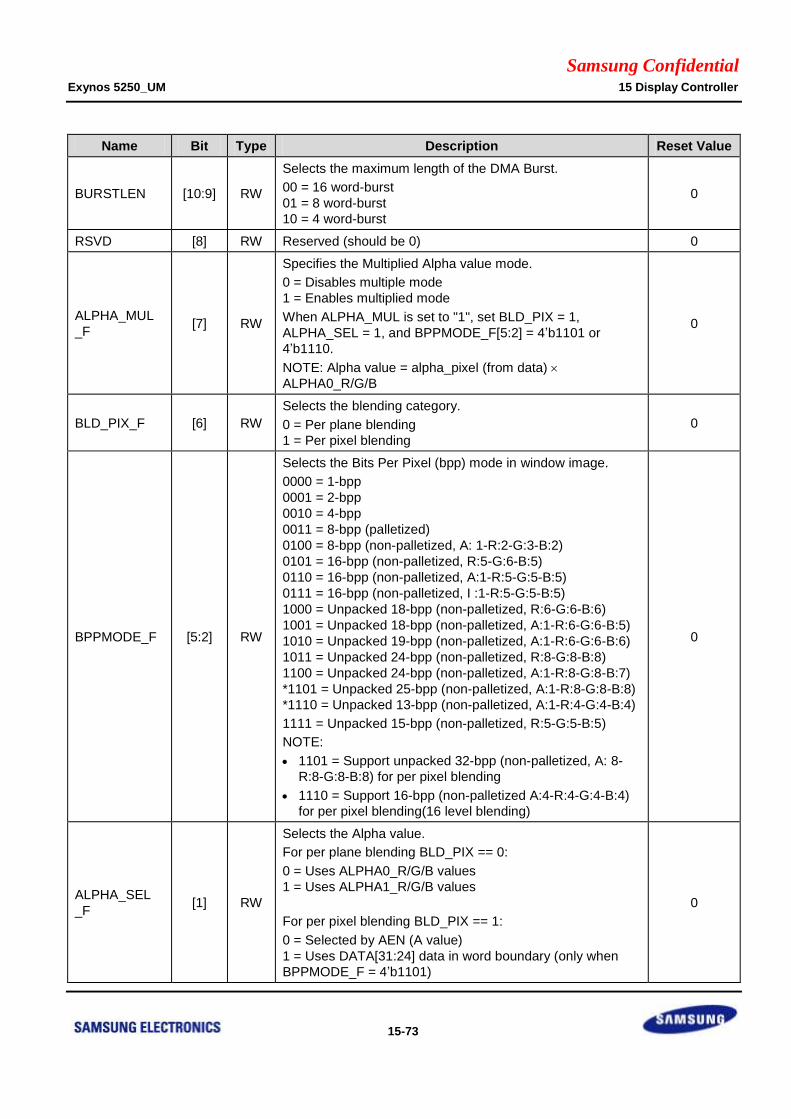
Samsung Confidential Exynos 5250_UM 15 Display Controller
15-73
Name Bit Type Description Reset Value
BURSTLEN [10:9] RW
Selects the maximum length of the DMA Burst.
00 = 16 word-burst
01 = 8 word-burst
10 = 4 word-burst
0
RSVD [8] RW Reserved (should be 0) 0
ALPHA_MUL
_F [7] RW
Specifies the Multiplied Alpha value mode.
0 = Disables multiple mode
1 = Enables multiplied mode
When ALPHA_MUL is set to "1", set BLD_PIX = 1,
ALPHA_SEL = 1, and BPPMODE_F[5:2] = 4’b1101 or
4’b1110.
NOTE: Alpha value = alpha_pixel (from data)
ALPHA0_R/G/B
0
BLD_PIX_F [6] RW
Selects the blending category.
0 = Per plane blending
1 = Per pixel blending
0
BPPMODE_F [5:2] RW
Selects the Bits Per Pixel (bpp) mode in window image.
0000 = 1-bpp
0001 = 2-bpp
0010 = 4-bpp
0011 = 8-bpp (palletized)
0100 = 8-bpp (non-palletized, A: 1-R:2-G:3-B:2)
0101 = 16-bpp (non-palletized, R:5-G:6-B:5)
0110 = 16-bpp (non-palletized, A:1-R:5-G:5-B:5)
0111 = 16-bpp (non-palletized, I :1-R:5-G:5-B:5)
1000 = Unpacked 18-bpp (non-palletized, R:6-G:6-B:6)
1001 = Unpacked 18-bpp (non-palletized, A:1-R:6-G:6-B:5)
1010 = Unpacked 19-bpp (non-palletized, A:1-R:6-G:6-B:6)
1011 = Unpacked 24-bpp (non-palletized, R:8-G:8-B:8)
1100 = Unpacked 24-bpp (non-palletized, A:1-R:8-G:8-B:7)
*1101 = Unpacked 25-bpp (non-palletized, A:1-R:8-G:8-B:8)
*1110 = Unpacked 13-bpp (non-palletized, A:1-R:4-G:4-B:4)
1111 = Unpacked 15-bpp (non-palletized, R:5-G:5-B:5)
NOTE:
1101 = Support unpacked 32-bpp (non-palletized, A: 8-
R:8-G:8-B:8) for per pixel blending
1110 = Support 16-bpp (non-palletized A:4-R:4-G:4-B:4)
for per pixel blending(16 level blending)
0
ALPHA_SEL
_F [1] RW
Selects the Alpha value.
For per plane blending BLD_PIX == 0:
0 = Uses ALPHA0_R/G/B values
1 = Uses ALPHA1_R/G/B values
For per pixel blending BLD_PIX == 1:
0 = Selected by AEN (A value)
1 = Uses DATA[31:24] data in word boundary (only when
BPPMODE_F = 4’b1101)
0
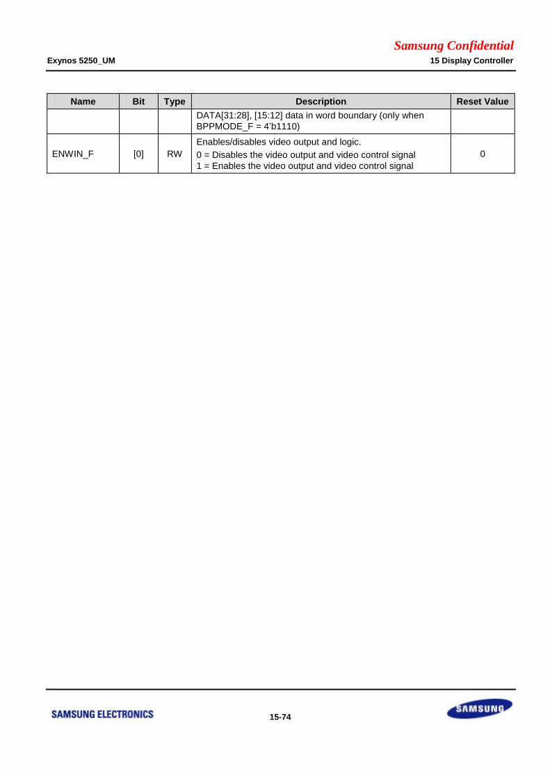
Samsung Confidential Exynos 5250_UM 15 Display Controller
15-74
Name Bit Type Description Reset Value
DATA[31:28], [15:12] data in word boundary (only when
BPPMODE_F = 4’b1110)
ENWIN_F [0] RW
Enables/disables video output and logic.
0 = Disables the video output and video control signal
1 = Enables the video output and video control signal
0
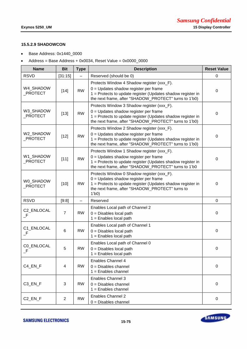
Samsung Confidential Exynos 5250_UM 15 Display Controller
15-75
15.5.2.9 SHADOWCON
Base Address: 0x1440_0000
Address = Base Address + 0x0034, Reset Value = 0x0000_0000
Name Bit Type Description Reset Value
RSVD [31:15] – Reserved (should be 0) 0
W4_SHADOW
_PROTECT [14] RW
Protects Window 4 Shadow register (xxx_F).
0 = Updates shadow register per frame
1 = Protects to update register (Updates shadow register in
the next frame, after "SHADOW_PROTECT" turns to 1’b0)
0
W3_SHADOW
_PROTECT [13] RW
Protects Window 3 Shadow register (xxx_F).
0 = Updates shadow register per frame
1 = Protects to update register (Updates shadow register in
the next frame, after "SHADOW_PROTECT" turns to 1’b0)
0
W2_SHADOW
_PROTECT [12] RW
Protects Window 2 Shadow register (xxx_F).
0 = Updates shadow register per frame
1 = Protects to update register (Updates shadow register in
the next frame, after "SHADOW_PROTECT" turns to 1’b0)
0
W1_SHADOW
_PROTECT [11] RW
Protects Window 1 Shadow register (xxx_F).
0 = Updates shadow register per frame
1 = Protects to update register (Updates shadow register in
the next frame, after "SHADOW_PROTECT" turns to 1’b0
0
W0_SHADOW
_PROTECT [10] RW
Protects Window 0 Shadow register (xxx_F).
0 = Updates shadow register per frame
1 = Protects to update register (Updates shadow register in
the next frame, after "SHADOW_PROTECT" turns to
1’b0)
0
RSVD [9:8] – Reserved 0
C2_ENLOCAL
_F 7 RW
Enables Local path of Channel 2
0 = Disables local path
1 = Enables local path
0
C1_ENLOCAL
_F 6 RW
Enables Local path of Channel 1
0 = Disables local path
1 = Enables local path
0
C0_ENLOCAL
_F 5 RW
Enables Local path of Channel 0
0 = Disables local path
1 = Enables local path
0
C4_EN_F 4 RW
Enables Channel 4
0 = Disables channel
1 = Enables channel
0
C3_EN_F 3 RW
Enables Channel 3
0 = Disables channel
1 = Enables channel
0
C2_EN_F 2 RW Enables Channel 2
0 = Disables channel 0
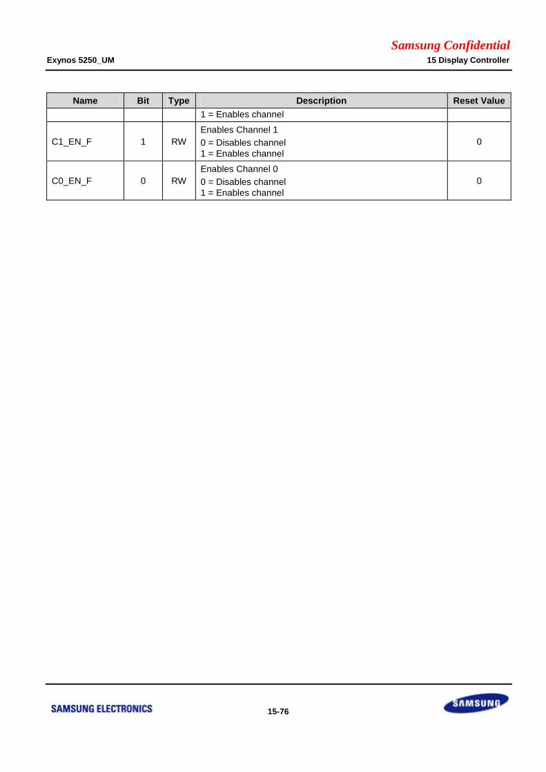
Samsung Confidential Exynos 5250_UM 15 Display Controller
15-76
Name Bit Type Description Reset Value
1 = Enables channel
C1_EN_F 1 RW
Enables Channel 1
0 = Disables channel
1 = Enables channel
0
C0_EN_F 0 RW
Enables Channel 0
0 = Disables channel
1 = Enables channel
0
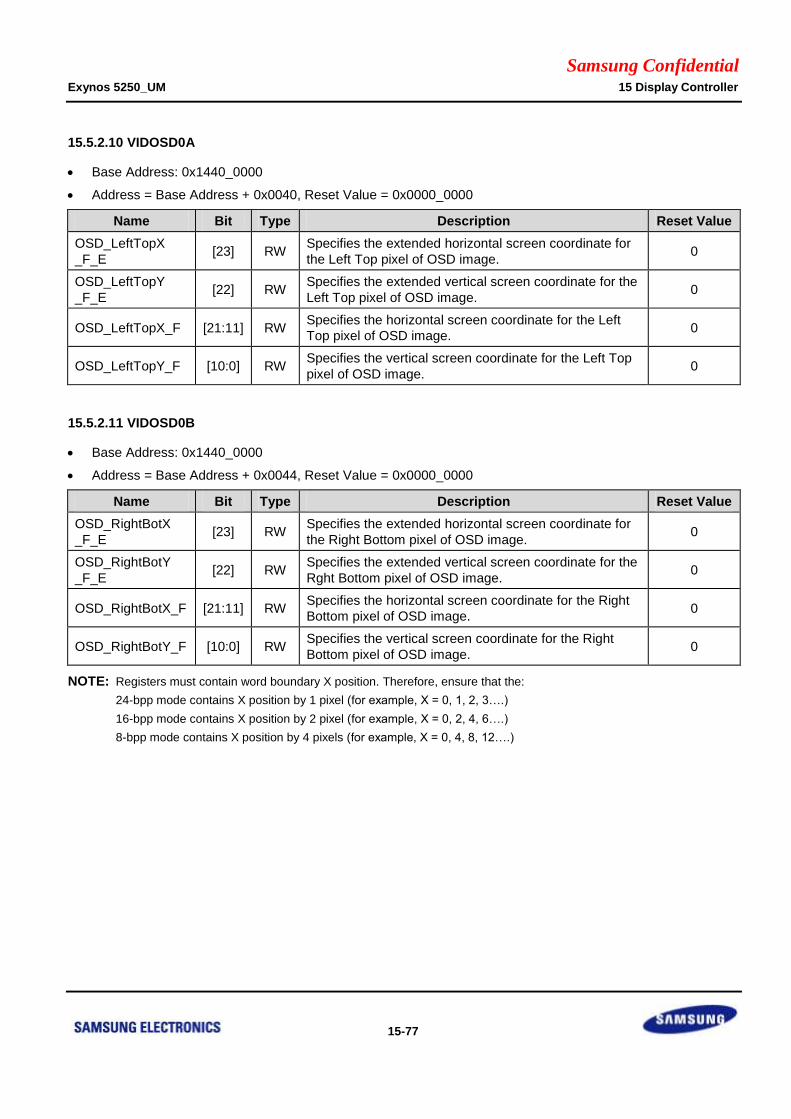
Samsung Confidential Exynos 5250_UM 15 Display Controller
15-77
15.5.2.10 VIDOSD0A
Base Address: 0x1440_0000
Address = Base Address + 0x0040, Reset Value = 0x0000_0000
Name Bit Type Description Reset Value
OSD_LeftTopX
_F_E [23] RW
Specifies the extended horizontal screen coordinate for
the Left Top pixel of OSD image. 0
OSD_LeftTopY
_F_E [22] RW
Specifies the extended vertical screen coordinate for the
Left Top pixel of OSD image. 0
OSD_LeftTopX_F [21:11] RW Specifies the horizontal screen coordinate for the Left
Top pixel of OSD image. 0
OSD_LeftTopY_F [10:0] RW Specifies the vertical screen coordinate for the Left Top
pixel of OSD image. 0
15.5.2.11 VIDOSD0B
Base Address: 0x1440_0000
Address = Base Address + 0x0044, Reset Value = 0x0000_0000
Name Bit Type Description Reset Value
OSD_RightBotX
_F_E [23] RW
Specifies the extended horizontal screen coordinate for
the Right Bottom pixel of OSD image. 0
OSD_RightBotY
_F_E [22] RW
Specifies the extended vertical screen coordinate for the
Rght Bottom pixel of OSD image. 0
OSD_RightBotX_F [21:11] RW Specifies the horizontal screen coordinate for the Right
Bottom pixel of OSD image. 0
OSD_RightBotY_F [10:0] RW Specifies the vertical screen coordinate for the Right
Bottom pixel of OSD image. 0
NOTE: Registers must contain word boundary X position. Therefore, ensure that the:
24-bpp mode contains X position by 1 pixel (for example, X = 0, 1, 2, 3….)
16-bpp mode contains X position by 2 pixel (for example, X = 0, 2, 4, 6….)
8-bpp mode contains X position by 4 pixels (for example, X = 0, 4, 8, 12….)

Samsung Confidential Exynos 5250_UM 15 Display Controller
15-78
15.5.2.12 VIDOSD0C
Base Address: 0x1440_0000
Address = Base Address + 0x0048, Reset Value = 0x0000_0000
Name Bit Type Description Reset Value
RSVD [25:24] – Reserved (should be 0) 0
OSDSIZE [23:0] RW Specifies the Window Size.
For example, Height Width (number of words) 0
15.5.2.13 VIDOSD1A
Base Address: 0x1440_0000
Address = Base Address + 0x0050, Reset Value = 0x0000_0000
Name Bit Type Description Reset Value
OSD_LeftTopX
_F_E [23] RW
Specifies the extended horizontal screen coordinate for
the Left Top pixel of OSD image. 0
OSD_LeftTopY
_F_E [22] RW
Specifies the extended vertical screen coordinate for
the Left Top pixel of OSD image. 0
OSD_LeftTopX_F [21:11] RW Specifies the horizontal screen coordinate for the Left
Top pixel of OSD image. 0
OSD_LeftTopY_F [10:0] RW Specifies the vertical screen coordinate for the Left Top
pixel of OSD image. 0

Samsung Confidential Exynos 5250_UM 15 Display Controller
15-79
15.5.2.14 VIDOSD1B
Base Address: 0x1440_0000
Address = Base Address + 0x0054, Reset Value = 0x0000_0000
Name Bit Type Description Reset Value
OSD_RightBotX
_F_E [23] RW
Specifies the extended horizontal screen coordinate for
the Right Bottom pixel of OSD image. 0
OSD_RightBotY
_F_E [22] RW
Specifies the extended vertical screen coordinate for
the Right Bottom pixel of OSD image. 0
OSD_RightBotX
_F [21:11] RW
Specifies the horizontal screen coordinate for the Right
Bottom pixel of OSD image. 0
OSD_RightBotY
_F [10:0] RW
Specifies the vertical screen coordinate for the Right
Bottom pixel of OSD image. 0
NOTE: Registers must contain word boundary X position.
Therefore, ensure that the:
24-bpp mode contains X position by 1 pixel (for example, X = 0, 1, 2, 3….)
16-bpp mode contains X position by 2 pixel (for example, X = 0, 2, 4, 6….)
8-bpp mode contains X position by 4 pixel (for example, X = 0, 4, 8, 12….)
15.5.2.15 VIDOSD1C
Base Address: 0x1440_0000
Address = Base Address + 0x0058, Reset Value = 0x0000_0000
Name Bit Type Description Reset Value
RSVD [24] – Reserved 0
ALPHA0_R_H_F [23:20] RW Specifies the upper value of Red Alpha (case AEN ==
0) 0
ALPHA0_G_H_F [19:16] RW Specifies the upper value of Green Alpha (case AEN
== 0) 0
ALPHA0_B_H_F [15:12] RW Specifies the upper value of Blue Alpha (case AEN ==
0) 0
ALPHA1_R_H_F [11:8] RW Specifies the upper value of Red Alpha (case AEN ==
1) 0
ALPHA1_G_H_F [7:4] RW Specifies the upper value of Green Alpha (case AEN
== 1) 0
ALPHA1_B_H_F [3:0] RW Specifies the upper value of Blue Alpha (case AEN ==
1) 0
NOTE: Refer to VIDW1ALPHA0, 1 register for more information.
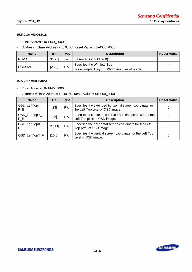
Samsung Confidential Exynos 5250_UM 15 Display Controller
15-80
15.5.2.16 VIDOSD1D
Base Address: 0x1440_0000
Address = Base Address + 0x005C, Reset Value = 0x0000_0000
Name Bit Type Description Reset Value
RSVD [31:26] – Reserved (should be 0) 0
OSDSIZE [25:0] RW Specifies the Window Size.
For example, Height Width (number of words) 0
15.5.2.17 VIDOSD2A
Base Address: 0x1440_0000
Address = Base Address + 0x0060, Reset Value = 0x0000_0000
Name Bit Type Description Reset Value
OSD_LeftTopX_
F_E [23] RW
Specifies the extended horizontal screen coordinate for
the Left Top pixel of OSD image. 0
OSD_LeftTopY_
F_E [22] RW
Specifies the extended vertical screen coordinate for the
Left Top pixel of OSD image. 0
OSD_LeftTopX_
F [21:11] RW
Specifies the horizontal screen coordinate for the Left
Top pixel of OSD image. 0
OSD_LeftTopY_F [10:0] RW Specifies the vertical screen coordinate for the Left Top
pixel of OSD image. 0
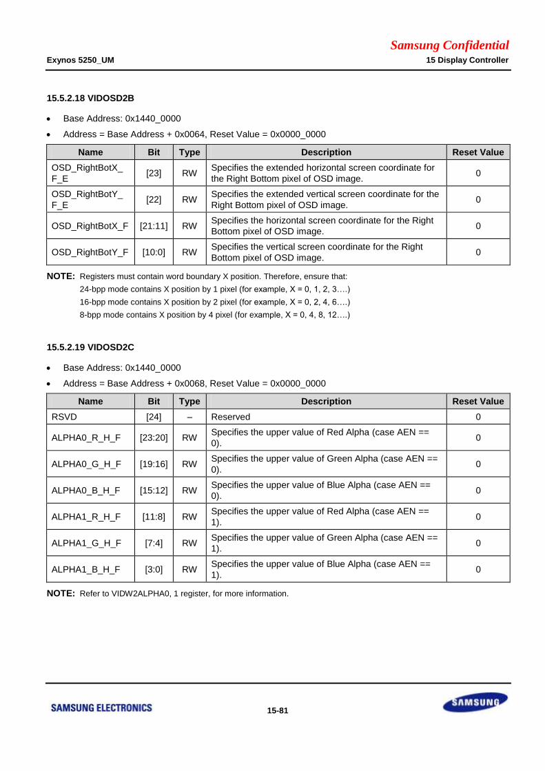
Samsung Confidential Exynos 5250_UM 15 Display Controller
15-81
15.5.2.18 VIDOSD2B
Base Address: 0x1440_0000
Address = Base Address + 0x0064, Reset Value = 0x0000_0000
Name Bit Type Description Reset Value
OSD_RightBotX_
F_E [23] RW
Specifies the extended horizontal screen coordinate for
the Right Bottom pixel of OSD image. 0
OSD_RightBotY_
F_E [22] RW
Specifies the extended vertical screen coordinate for the
Right Bottom pixel of OSD image. 0
OSD_RightBotX_F [21:11] RW Specifies the horizontal screen coordinate for the Right
Bottom pixel of OSD image. 0
OSD_RightBotY_F [10:0] RW Specifies the vertical screen coordinate for the Right
Bottom pixel of OSD image. 0
NOTE: Registers must contain word boundary X position. Therefore, ensure that:
24-bpp mode contains X position by 1 pixel (for example, X = 0, 1, 2, 3….)
16-bpp mode contains X position by 2 pixel (for example, X = 0, 2, 4, 6….)
8-bpp mode contains X position by 4 pixel (for example, X = 0, 4, 8, 12….)
15.5.2.19 VIDOSD2C
Base Address: 0x1440_0000
Address = Base Address + 0x0068, Reset Value = 0x0000_0000
Name Bit Type Description Reset Value
RSVD [24] – Reserved 0
ALPHA0_R_H_F [23:20] RW Specifies the upper value of Red Alpha (case AEN ==
0). 0
ALPHA0_G_H_F [19:16] RW Specifies the upper value of Green Alpha (case AEN ==
0). 0
ALPHA0_B_H_F [15:12] RW Specifies the upper value of Blue Alpha (case AEN ==
0). 0
ALPHA1_R_H_F [11:8] RW Specifies the upper value of Red Alpha (case AEN ==
1). 0
ALPHA1_G_H_F [7:4] RW Specifies the upper value of Green Alpha (case AEN ==
1). 0
ALPHA1_B_H_F [3:0] RW Specifies the upper value of Blue Alpha (case AEN ==
1). 0
NOTE: Refer to VIDW2ALPHA0, 1 register, for more information.

Samsung Confidential Exynos 5250_UM 15 Display Controller
15-82
15.5.2.20 VIDOSD2D
Base Address: 0x1440_0000
Address = Base Address + 0x006C, Reset Value = 0x0000_0000
Name Bit Type Description Reset Value
RSVD [31:26] – Reserved (should be 0) 0
OSDSIZE [25:0] RW Specifies the Window Size.
For example, Height Width (number of words) 0
15.5.2.21 VIDOSD3A
Base Address: 0x1440_0000
Address = Base Address + 0x0070, Reset Value = 0x0000_0000
Name Bit Type Description Reset Value
OSD_LeftTopX_
F_E [23] RW
Specifies the extended horizontal screen coordinate for
the Left Top pixel of OSD image. 0
OSD_LeftTopY_
F_E [22] RW
Specifies the extended vertical screen coordinate for
the Left Top pixel of OSD image. 0
OSD_LeftTopX_F [21:11] RW Specifies the horizontal screen coordinate for the Left
Top pixel of OSD image. 0
OSD_LeftTopY_F [10:0] RW Specifies the vertical screen coordinate for the Left Top
pixel of OSD image. 0
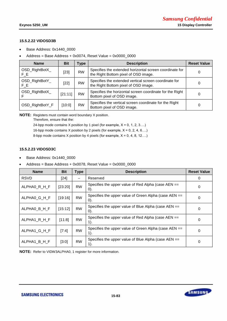
Samsung Confidential Exynos 5250_UM 15 Display Controller
15-83
15.5.2.22 VIDOSD3B
Base Address: 0x1440_0000
Address = Base Address + 0x0074, Reset Value = 0x0000_0000
Name Bit Type Description Reset Value
OSD_RightBotX_
F_E [23] RW
Specifies the extended horizontal screen coordinate for
the Right Bottom pixel of OSD image. 0
OSD_RightBotY_
F_E [22] RW
Specifies the extended vertical screen coordinate for
the Right Bottom pixel of OSD image. 0
OSD_RightBotX_
F [21:11] RW
Specifies the horizontal screen coordinate for the Right
Bottom pixel of OSD image. 0
OSD_RightBotY_F [10:0] RW Specifies the vertical screen coordinate for the Right
Bottom pixel of OSD image. 0
NOTE: Registers must contain word boundary X position.
Therefore, ensure that the:
24-bpp mode contains X position by 1 pixel (for example, X = 0, 1, 2, 3….)
16-bpp mode contains X position by 2 pixels (for example, X = 0, 2, 4, 6….)
8-bpp mode contains X position by 4 pixels (for example, X = 0, 4, 8, 12….)
15.5.2.23 VIDOSD3C
Base Address: 0x1440_0000
Address = Base Address + 0x0078, Reset Value = 0x0000_0000
Name Bit Type Description Reset Value
RSVD [24] – Reserved 0
ALPHA0_R_H_F [23:20] RW Specifies the upper value of Red Alpha (case AEN ==
0). 0
ALPHA0_G_H_F [19:16] RW Specifies the upper value of Green Alpha (case AEN ==
0). 0
ALPHA0_B_H_F [15:12] RW Specifies the upper value of Blue Alpha (case AEN ==
0). 0
ALPHA1_R_H_F [11:8] RW Specifies the upper value of Red Alpha (case AEN ==
1). 0
ALPHA1_G_H_F [7:4] RW Specifies the upper value of Green Alpha (case AEN ==
1). 0
ALPHA1_B_H_F [3:0] RW Specifies the upper value of Blue Alpha (case AEN ==
1). 0
NOTE: Refer to VIDW3ALPHA0, 1 register for more information.
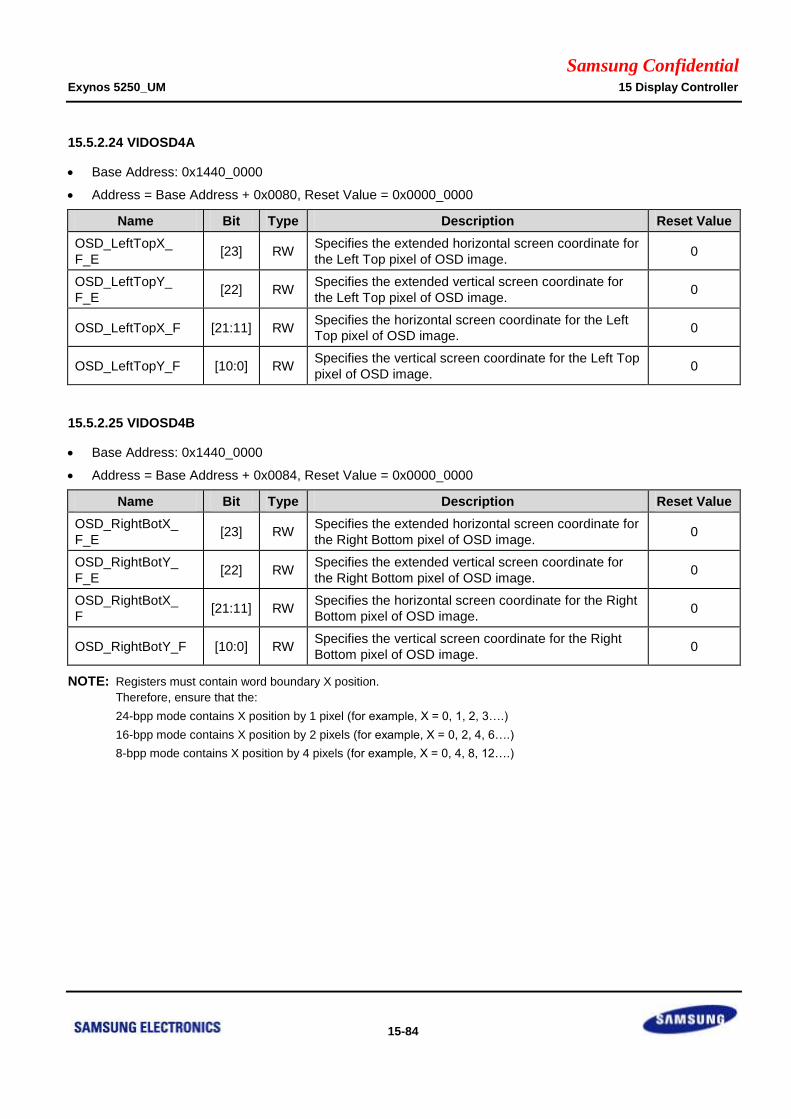
Samsung Confidential Exynos 5250_UM 15 Display Controller
15-84
15.5.2.24 VIDOSD4A
Base Address: 0x1440_0000
Address = Base Address + 0x0080, Reset Value = 0x0000_0000
Name Bit Type Description Reset Value
OSD_LeftTopX_
F_E [23] RW
Specifies the extended horizontal screen coordinate for
the Left Top pixel of OSD image. 0
OSD_LeftTopY_
F_E [22] RW
Specifies the extended vertical screen coordinate for
the Left Top pixel of OSD image. 0
OSD_LeftTopX_F [21:11] RW Specifies the horizontal screen coordinate for the Left
Top pixel of OSD image. 0
OSD_LeftTopY_F [10:0] RW Specifies the vertical screen coordinate for the Left Top
pixel of OSD image. 0
15.5.2.25 VIDOSD4B
Base Address: 0x1440_0000
Address = Base Address + 0x0084, Reset Value = 0x0000_0000
Name Bit Type Description Reset Value
OSD_RightBotX_
F_E [23] RW
Specifies the extended horizontal screen coordinate for
the Right Bottom pixel of OSD image. 0
OSD_RightBotY_
F_E [22] RW
Specifies the extended vertical screen coordinate for
the Right Bottom pixel of OSD image. 0
OSD_RightBotX_
F [21:11] RW
Specifies the horizontal screen coordinate for the Right
Bottom pixel of OSD image. 0
OSD_RightBotY_F [10:0] RW Specifies the vertical screen coordinate for the Right
Bottom pixel of OSD image. 0
NOTE: Registers must contain word boundary X position.
Therefore, ensure that the:
24-bpp mode contains X position by 1 pixel (for example, X = 0, 1, 2, 3….)
16-bpp mode contains X position by 2 pixels (for example, X = 0, 2, 4, 6….)
8-bpp mode contains X position by 4 pixels (for example, X = 0, 4, 8, 12….)
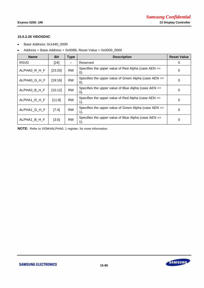
Samsung Confidential Exynos 5250_UM 15 Display Controller
15-85
15.5.2.26 VIDOSD4C
Base Address: 0x1440_0000
Address = Base Address + 0x0088, Reset Value = 0x0000_0000
Name Bit Type Description Reset Value
RSVD [24] – Reserved 0
ALPHA0_R_H_F [23:20] RW Specifies the upper value of Red Alpha (case AEN ==
0). 0
ALPHA0_G_H_F [19:16] RW Specifies the upper value of Green Alpha (case AEN ==
0). 0
ALPHA0_B_H_F [15:12] RW Specifies the upper value of Blue Alpha (case AEN ==
0). 0
ALPHA1_R_H_F [11:8] RW Specifies the upper value of Red Alpha (case AEN ==
1). 0
ALPHA1_G_H_F [7:4] RW Specifies the upper value of Green Alpha (case AEN ==
1). 0
ALPHA1_B_H_F [3:0] RW Specifies the upper value of Blue Alpha (case AEN ==
1). 0
NOTE: Refer to VIDW4ALPHA0, 1 register, for more information.
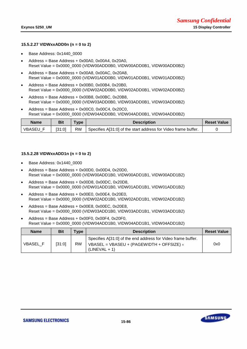
Samsung Confidential Exynos 5250_UM 15 Display Controller
15-86
15.5.2.27 VIDWxxADD0n (n = 0 to 2)
Base Address: 0x1440_0000
Address = Base Address + 0x00A0, 0x00A4, 0x20A0,
Reset Value = 0x0000_0000 (VIDW00ADD0B0, VIDW00ADD0B1, VIDW00ADD0B2)
Address = Base Address + 0x00A8, 0x00AC, 0x20A8,
Reset Value = 0x0000_0000 (VIDW01ADD0B0, VIDW01ADD0B1, VIDW01ADD0B2)
Address = Base Address + 0x00B0, 0x00B4, 0x20B0,
Reset Value = 0x0000_0000 (VIDW02ADD0B0, VIDW02ADD0B1, VIDW02ADD0B2)
Address = Base Address + 0x00B8, 0x00BC, 0x20B8,
Reset Value = 0x0000_0000 (VIDW03ADD0B0, VIDW03ADD0B1, VIDW03ADD0B2)
Address = Base Address + 0x00C0, 0x00C4, 0x20C0,
Reset Value = 0x0000_0000 (VIDW04ADD0B0, VIDW04ADD0B1, VIDW04ADD0B2)
Name Bit Type Description Reset Value
VBASEU_F [31:0] RW Specifies A[31:0] of the start address for Video frame buffer. 0
15.5.2.28 VIDWxxADD1n (n = 0 to 2)
Base Address: 0x1440_0000
Address = Base Address + 0x00D0, 0x00D4, 0x20D0,
Reset Value = 0x0000_0000 (VIDW00ADD1B0, VIDW00ADD1B1, VIDW00ADD1B2)
Address = Base Address + 0x00D8, 0x00DC, 0x20D8,
Reset Value = 0x0000_0000 (VIDW01ADD1B0, VIDW01ADD1B1, VIDW01ADD1B2)
Address = Base Address + 0x00E0, 0x00E4, 0x20E0,
Reset Value = 0x0000_0000 (VIDW02ADD1B0, VIDW02ADD1B1, VIDW02ADD1B2)
Address = Base Address + 0x00E8, 0x00EC, 0x20E8,
Reset Value = 0x0000_0000 (VIDW03ADD1B0, VIDW03ADD1B1, VIDW03ADD1B2)
Address = Base Address + 0x00F0, 0x00F4, 0x20F0,
Reset Value = 0x0000_0000 (VIDW04ADD1B0, VIDW04ADD1B1, VIDW04ADD1B2)
Name Bit Type Description Reset Value
VBASEL_F [31:0] RW
Specifies A[31:0] of the end address for Video frame buffer.
VBASEL = VBASEU + (PAGEWIDTH + OFFSIZE)
(LINEVAL + 1)
0x0
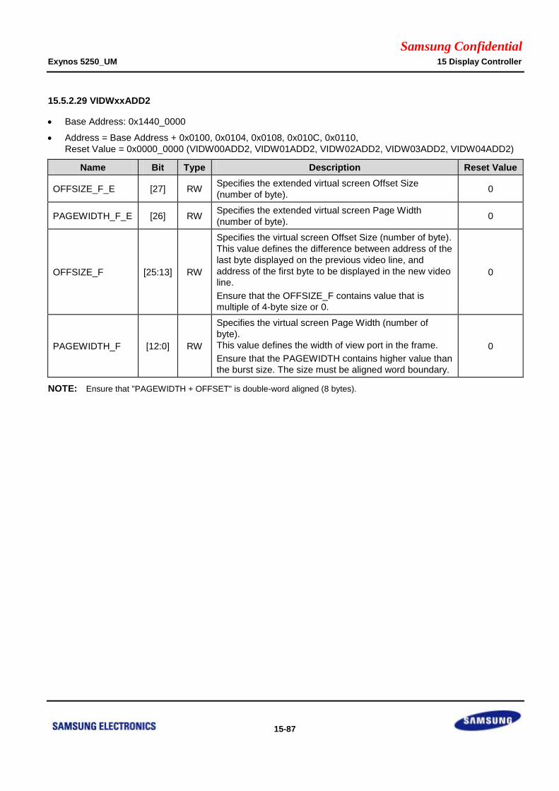
Samsung Confidential Exynos 5250_UM 15 Display Controller
15-87
15.5.2.29 VIDWxxADD2
Base Address: 0x1440_0000
Address = Base Address + 0x0100, 0x0104, 0x0108, 0x010C, 0x0110,
Reset Value = 0x0000_0000 (VIDW00ADD2, VIDW01ADD2, VIDW02ADD2, VIDW03ADD2, VIDW04ADD2)
Name Bit Type Description Reset Value
OFFSIZE_F_E [27] RW Specifies the extended virtual screen Offset Size
(number of byte). 0
PAGEWIDTH_F_E [26] RW Specifies the extended virtual screen Page Width
(number of byte). 0
OFFSIZE_F [25:13] RW
Specifies the virtual screen Offset Size (number of byte).
This value defines the difference between address of the
last byte displayed on the previous video line, and
address of the first byte to be displayed in the new video
line.
Ensure that the OFFSIZE_F contains value that is
multiple of 4-byte size or 0.
0
PAGEWIDTH_F [12:0] RW
Specifies the virtual screen Page Width (number of
byte).
This value defines the width of view port in the frame.
Ensure that the PAGEWIDTH contains higher value than
the burst size. The size must be aligned word boundary.
0
NOTE: Ensure that "PAGEWIDTH + OFFSET" is double-word aligned (8 bytes).

Samsung Confidential Exynos 5250_UM 15 Display Controller
15-88
15.5.2.30 VIDINTCON0
Base Address: 0x1440_0000
Address = Base Address + 0x0130, Reset Value = 0x0000_0000
Name Bit Type Description Reset Value
RSVD [31:26] – Reserved 0
FIFOINTERVAL [25:20] RW Controls the interval of the FIFO interrupt. 0
SYSMAINCON [19] RW
Sends complete interrupt enable bit to Main LCD
0 = Disables Interrupt
1 = Enables Interrupt
NOTE: This bit is meaningful if both INTEN and
I80IFDONE are high.
0
SYSSUBCON [18] RW
Sends complete interrupt enable bit to Sub LCD
0 = Disables Interrupt.
1 = Enables Interrupt.
NOTE: This bit is meaningful if both INTEN and
I80IFDONE are high.
0
I80IFDONE [17] RW
Enables the I80 Interface Interrupt (only for I80 Interface
mode).
0 = Disables Interrupt.
1 = Enables Interrupt.
NOTE: This bit is meaningful if INTEN is high.
0
FRAMESEL0 [16:15] RW
Specifies the Video Frame Interrupt 0 at start of:
00 = BACK Porch
01 = VSYNC
10 = ACTIVE
11 = FRONT Porch
0
FRAMESEL1 [14:13] RW
Specifies the Video Frame Interrupt 1 at start of:
00 = None
01 = BACK Porch
10 = VSYNC
11 = FRONT Porch
0
INTFRMEN [12] RW
Specifies the Video Frame Interrupt enable control bit.
0 = Disables video frame interrupt
1 = Enables video frame interrupt
NOTE: This bit is significant, when INTEN is high.
0
FIFOSEL [11:5] RW
Specifies the FIFO Interrupt control bit. Each bit contains
a significance:
[11] Window 4 control (0 = disables, 1 = enables)
[10] Window 3 control (0 = disables, 1 = enables)
[9] Window 2 control (0 = disables, 1 = enables)
[8] Reserved
[7] Reserved
[6] Window 1 control (0 = disables, 1 = enables)
[5] Window 0 control (0 = disables, 1 = enables)
NOTE: This bit is significant, when both INTEN and
0
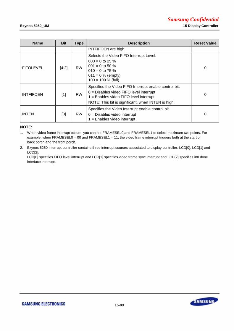
Samsung Confidential Exynos 5250_UM 15 Display Controller
15-89
Name Bit Type Description Reset Value
INTFIFOEN are high.
FIFOLEVEL [4:2] RW
Selects the Video FIFO Interrupt Level.
000 = 0 to 25 %
001 = 0 to 50 %
010 = 0 to 75 %
011 = 0 % (empty)
100 = 100 % (full)
0
INTFIFOEN [1] RW
Specifies the Video FIFO Interrupt enable control bit.
0 = Disables video FIFO level interrupt
1 = Enables video FIFO level interrupt
NOTE: This bit is significant, when INTEN is high.
0
INTEN [0] RW
Specifies the Video Interrupt enable control bit.
0 = Disables video interrupt
1 = Enables video interrupt
0
NOTE:
1. When video frame interrupt occurs, you can set FRAMESEL0 and FRAMESEL1 to select maximum two points. For
example, when FRAMESEL0 = 00 and FRAMESEL1 = 11, the video frame interrupt triggers both at the start of
back porch and the front porch.
2. Exynos 5250 interrupt controller contains three interrupt sources associated to display controller: LCD[0], LCD[1] and
LCD[2].
LCD[0] specifies FIFO level interrupt and LCD[1] specifies video frame sync interrupt and LCD[2] specifies i80 done
interface interrupt.
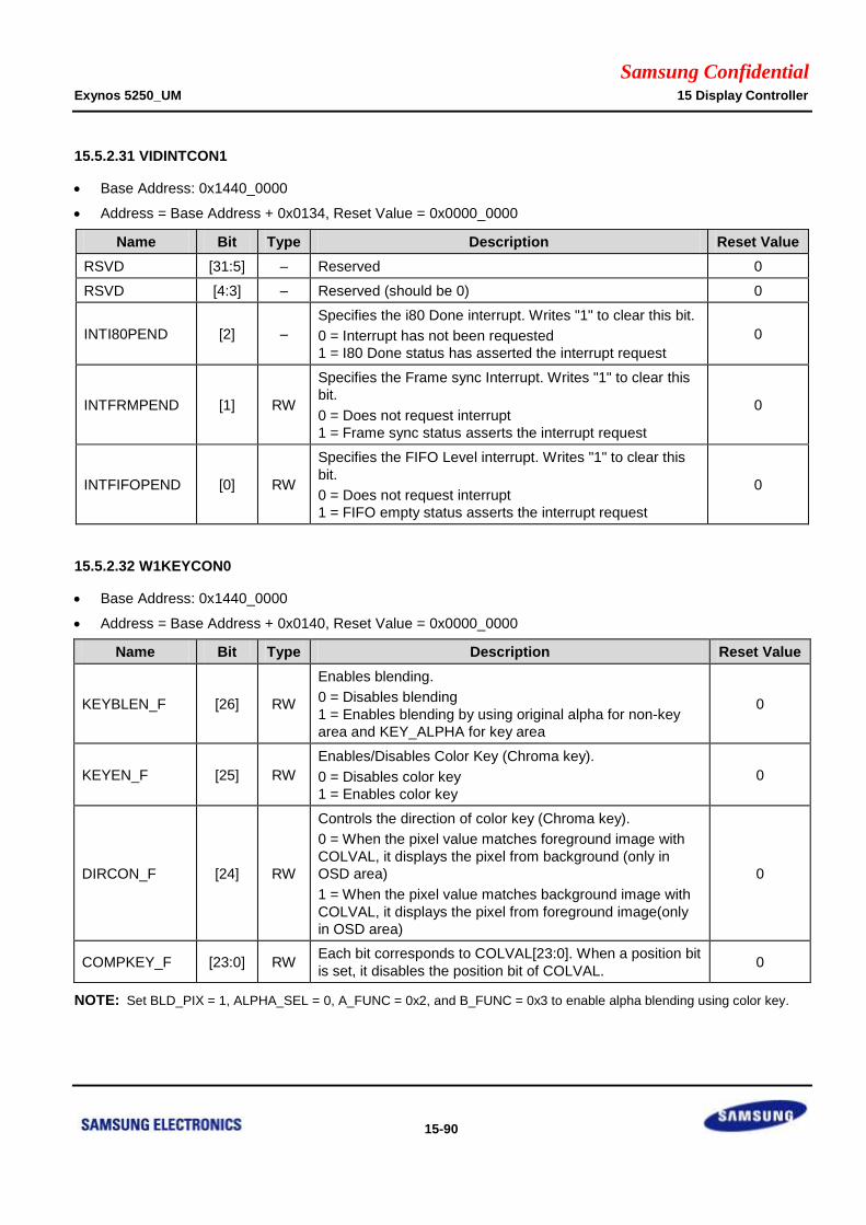
Samsung Confidential Exynos 5250_UM 15 Display Controller
15-90
15.5.2.31 VIDINTCON1
Base Address: 0x1440_0000
Address = Base Address + 0x0134, Reset Value = 0x0000_0000
Name Bit Type Description Reset Value
RSVD [31:5] – Reserved 0
RSVD [4:3] – Reserved (should be 0) 0
INTI80PEND [2] –
Specifies the i80 Done interrupt. Writes "1" to clear this bit.
0 = Interrupt has not been requested
1 = I80 Done status has asserted the interrupt request
0
INTFRMPEND [1] RW
Specifies the Frame sync Interrupt. Writes "1" to clear this
bit.
0 = Does not request interrupt
1 = Frame sync status asserts the interrupt request
0
INTFIFOPEND [0] RW
Specifies the FIFO Level interrupt. Writes "1" to clear this
bit.
0 = Does not request interrupt
1 = FIFO empty status asserts the interrupt request
0
15.5.2.32 W1KEYCON0
Base Address: 0x1440_0000
Address = Base Address + 0x0140, Reset Value = 0x0000_0000
Name Bit Type Description Reset Value
KEYBLEN_F [26] RW
Enables blending.
0 = Disables blending
1 = Enables blending by using original alpha for non-key
area and KEY_ALPHA for key area
0
KEYEN_F [25] RW
Enables/Disables Color Key (Chroma key).
0 = Disables color key
1 = Enables color key
0
DIRCON_F [24] RW
Controls the direction of color key (Chroma key).
0 = When the pixel value matches foreground image with
COLVAL, it displays the pixel from background (only in
OSD area)
1 = When the pixel value matches background image with
COLVAL, it displays the pixel from foreground image(only
in OSD area)
0
COMPKEY_F [23:0] RW Each bit corresponds to COLVAL[23:0]. When a position bit
is set, it disables the position bit of COLVAL. 0
NOTE: Set BLD_PIX = 1, ALPHA_SEL = 0, A_FUNC = 0x2, and B_FUNC = 0x3 to enable alpha blending using color key.
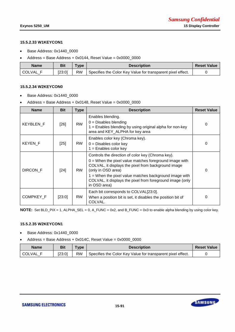
Samsung Confidential Exynos 5250_UM 15 Display Controller
15-91
15.5.2.33 W1KEYCON1
Base Address: 0x1440_0000
Address = Base Address + 0x0144, Reset Value = 0x0000_0000
Name Bit Type Description Reset Value
COLVAL_F [23:0] RW Specifies the Color Key Value for transparent pixel effect. 0
15.5.2.34 W2KEYCON0
Base Address: 0x1440_0000
Address = Base Address + 0x0148, Reset Value = 0x0000_0000
Name Bit Type Description Reset Value
KEYBLEN_F [26] RW
Enables blending.
0 = Disables blending
1 = Enables blending by using original alpha for non-key
area and KEY_ALPHA for key area
0
KEYEN_F [25] RW
Enables color key (Chroma key).
0 = Disables color key
1 = Enables color key
0
DIRCON_F [24] RW
Controls the direction of color key (Chroma key).
0 = When the pixel value matches foreground image with
COLVAL, it displays the pixel from background image
(only in OSD area)
1 = When the pixel value matches background image with
COLVAL, it displays the pixel from foreground image (only
in OSD area)
0
COMPKEY_F [23:0] RW
Each bit corresponds to COLVAL[23:0].
When a position bit is set, it disables the position bit of
COLVAL.
0
NOTE: Set BLD_PIX = 1, ALPHA_SEL = 0, A_FUNC = 0x2, and B_FUNC = 0x3 to enable alpha blending by using color key.
15.5.2.35 W2KEYCON1
Base Address: 0x1440_0000
Address = Base Address + 0x014C, Reset Value = 0x0000_0000
Name Bit Type Description Reset Value
COLVAL_F [23:0] RW Specifies the Color Key Value for transparent pixel effect. 0
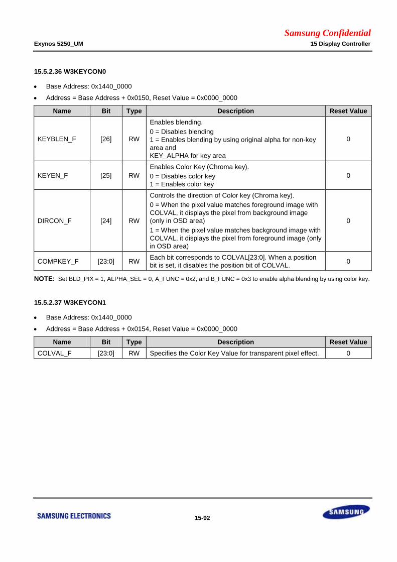
Samsung Confidential Exynos 5250_UM 15 Display Controller
15-92
15.5.2.36 W3KEYCON0
Base Address: 0x1440_0000
Address = Base Address + 0x0150, Reset Value = 0x0000_0000
Name Bit Type Description Reset Value
KEYBLEN_F [26] RW
Enables blending.
0 = Disables blending
1 = Enables blending by using original alpha for non-key
area and
KEY_ALPHA for key area
0
KEYEN_F [25] RW
Enables Color Key (Chroma key).
0 = Disables color key
1 = Enables color key
0
DIRCON_F [24] RW
Controls the direction of Color key (Chroma key).
0 = When the pixel value matches foreground image with
COLVAL, it displays the pixel from background image
(only in OSD area)
1 = When the pixel value matches background image with
COLVAL, it displays the pixel from foreground image (only
in OSD area)
0
COMPKEY_F [23:0] RW Each bit corresponds to COLVAL[23:0]. When a position
bit is set, it disables the position bit of COLVAL. 0
NOTE: Set BLD_PIX = 1, ALPHA_SEL = 0, A_FUNC = 0x2, and B_FUNC = 0x3 to enable alpha blending by using color key.
15.5.2.37 W3KEYCON1
Base Address: 0x1440_0000
Address = Base Address + 0x0154, Reset Value = 0x0000_0000
Name Bit Type Description Reset Value
COLVAL_F [23:0] RW Specifies the Color Key Value for transparent pixel effect. 0
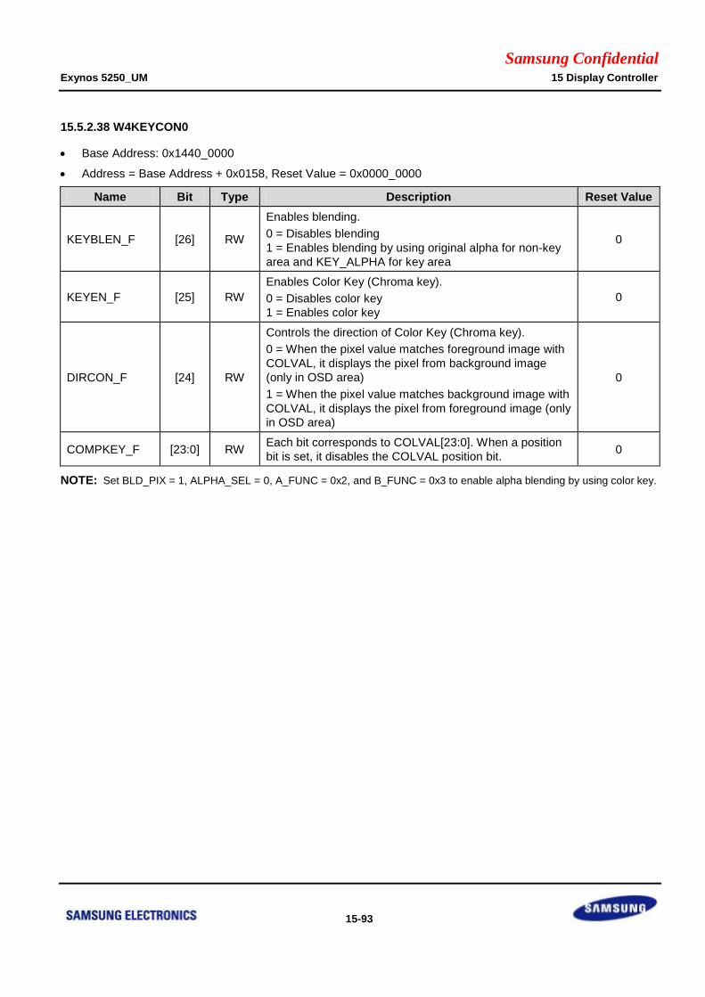
Samsung Confidential Exynos 5250_UM 15 Display Controller
15-93
15.5.2.38 W4KEYCON0
Base Address: 0x1440_0000
Address = Base Address + 0x0158, Reset Value = 0x0000_0000
Name Bit Type Description Reset Value
KEYBLEN_F [26] RW
Enables blending.
0 = Disables blending
1 = Enables blending by using original alpha for non-key
area and KEY_ALPHA for key area
0
KEYEN_F [25] RW
Enables Color Key (Chroma key).
0 = Disables color key
1 = Enables color key
0
DIRCON_F [24] RW
Controls the direction of Color Key (Chroma key).
0 = When the pixel value matches foreground image with
COLVAL, it displays the pixel from background image
(only in OSD area)
1 = When the pixel value matches background image with
COLVAL, it displays the pixel from foreground image (only
in OSD area)
0
COMPKEY_F [23:0] RW Each bit corresponds to COLVAL[23:0]. When a position
bit is set, it disables the COLVAL position bit. 0
NOTE: Set BLD_PIX = 1, ALPHA_SEL = 0, A_FUNC = 0x2, and B_FUNC = 0x3 to enable alpha blending by using color key.

Samsung Confidential Exynos 5250_UM 15 Display Controller
15-94
15.5.2.39 W4KEYCON1
Base Address: 0x1440_0000
Address = Base Address + 0x015C, Reset Value = 0x0000_0000
Name Bit Type Description Reset Value
COLVAL_F [23:0] RW Specifies the Color Key Value for transparent pixel effect. 0
NOTE: COLVAL and COMPKEY use 24-bit color data in all BPP modes.
At bpp -24 mode: 24-bit color value is valid
A. COLVAL
Red: COLVAL[23:17]
Green: COLVAL[15: 8]
Blue: COLVAL[7:0]
B. COMPKEY
Red: COMPKEY[23:17]
Green: COMPKEY[15: 8]
Blue: COMPKEY[7:0]
At bpp-16 (5:6:5) mode: 16-bit color value is valid
A. COLVAL
Red: COLVAL[23:19]
Green: COLVAL[15:10]
Blue: COLVAL[7:3]
B. COMPKEY
Red: COMPKEY[23:19]
Green: COMPKEY[15:10]
Blue: COMPKEY[7:3]
Ensure COMPKEY[18:16] is 0x7
Ensure COMPKEY[9: 8] is 0x3
Ensure COMPKEY[2:0] is 0x7
NOTE: Ensure to set the COMPKEY register appropriately for each BPP mode.
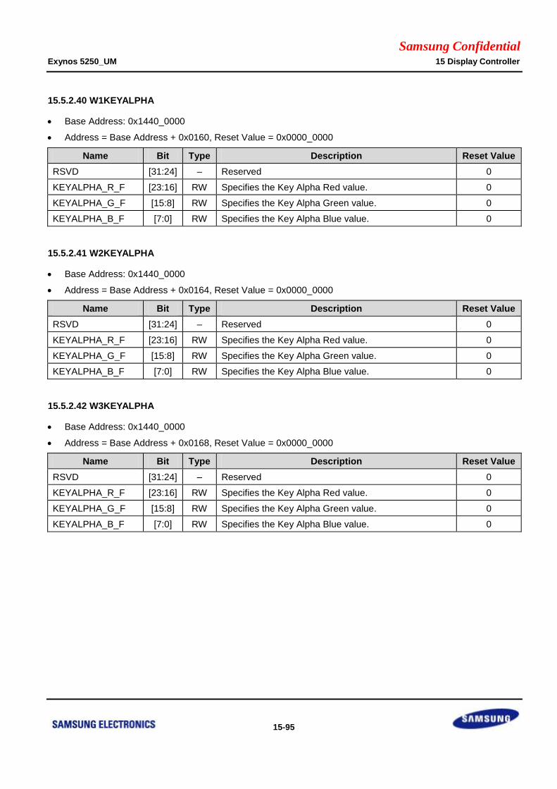
Samsung Confidential Exynos 5250_UM 15 Display Controller
15-95
15.5.2.40 W1KEYALPHA
Base Address: 0x1440_0000
Address = Base Address + 0x0160, Reset Value = 0x0000_0000
Name Bit Type Description Reset Value
RSVD [31:24] – Reserved 0
KEYALPHA_R_F [23:16] RW Specifies the Key Alpha Red value. 0
KEYALPHA_G_F [15:8] RW Specifies the Key Alpha Green value. 0
KEYALPHA_B_F [7:0] RW Specifies the Key Alpha Blue value. 0
15.5.2.41 W2KEYALPHA
Base Address: 0x1440_0000
Address = Base Address + 0x0164, Reset Value = 0x0000_0000
Name Bit Type Description Reset Value
RSVD [31:24] – Reserved 0
KEYALPHA_R_F [23:16] RW Specifies the Key Alpha Red value. 0
KEYALPHA_G_F [15:8] RW Specifies the Key Alpha Green value. 0
KEYALPHA_B_F [7:0] RW Specifies the Key Alpha Blue value. 0
15.5.2.42 W3KEYALPHA
Base Address: 0x1440_0000
Address = Base Address + 0x0168, Reset Value = 0x0000_0000
Name Bit Type Description Reset Value
RSVD [31:24] – Reserved 0
KEYALPHA_R_F [23:16] RW Specifies the Key Alpha Red value. 0
KEYALPHA_G_F [15:8] RW Specifies the Key Alpha Green value. 0
KEYALPHA_B_F [7:0] RW Specifies the Key Alpha Blue value. 0
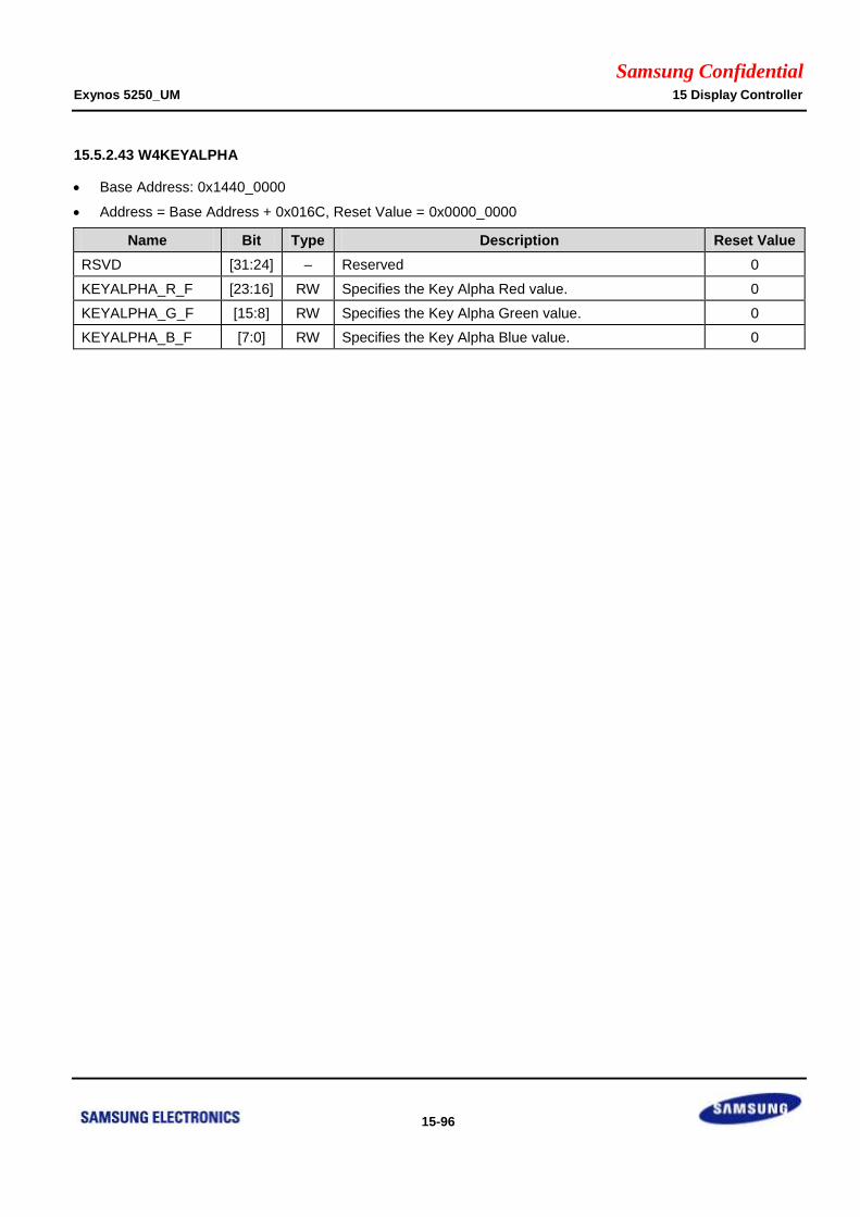
Samsung Confidential Exynos 5250_UM 15 Display Controller
15-96
15.5.2.43 W4KEYALPHA
Base Address: 0x1440_0000
Address = Base Address + 0x016C, Reset Value = 0x0000_0000
Name Bit Type Description Reset Value
RSVD [31:24] – Reserved 0
KEYALPHA_R_F [23:16] RW Specifies the Key Alpha Red value. 0
KEYALPHA_G_F [15:8] RW Specifies the Key Alpha Green value. 0
KEYALPHA_B_F [7:0] RW Specifies the Key Alpha Blue value. 0
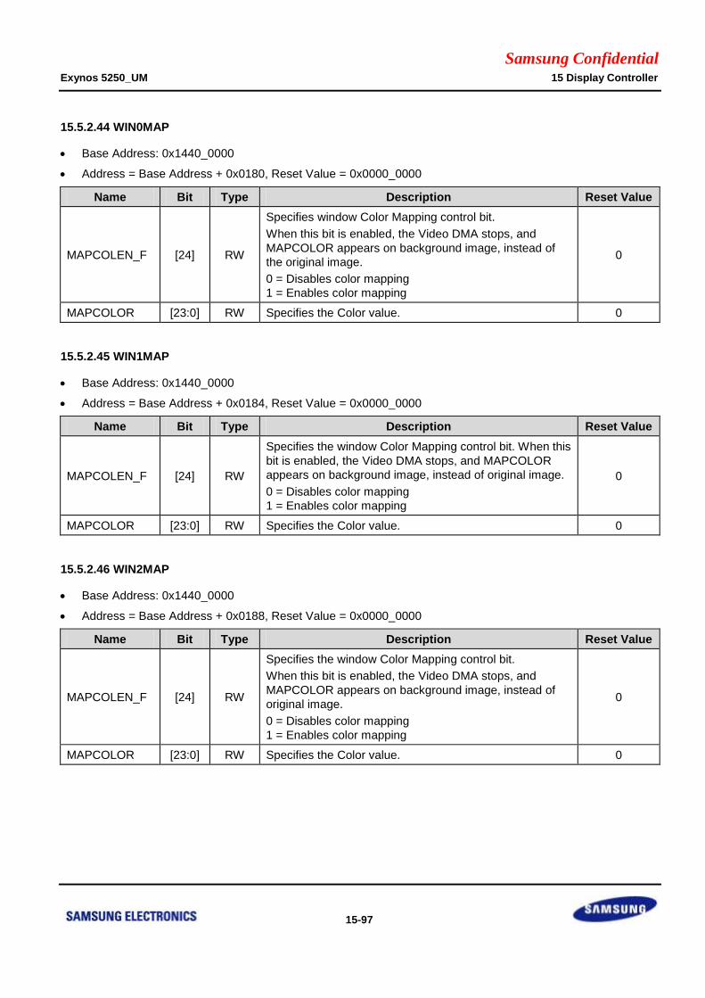
Samsung Confidential Exynos 5250_UM 15 Display Controller
15-97
15.5.2.44 WIN0MAP
Base Address: 0x1440_0000
Address = Base Address + 0x0180, Reset Value = 0x0000_0000
Name Bit Type Description Reset Value
MAPCOLEN_F [24] RW
Specifies window Color Mapping control bit.
When this bit is enabled, the Video DMA stops, and
MAPCOLOR appears on background image, instead of
the original image.
0 = Disables color mapping
1 = Enables color mapping
0
MAPCOLOR [23:0] RW Specifies the Color value. 0
15.5.2.45 WIN1MAP
Base Address: 0x1440_0000
Address = Base Address + 0x0184, Reset Value = 0x0000_0000
Name Bit Type Description Reset Value
MAPCOLEN_F [24] RW
Specifies the window Color Mapping control bit. When this
bit is enabled, the Video DMA stops, and MAPCOLOR
appears on background image, instead of original image.
0 = Disables color mapping
1 = Enables color mapping
0
MAPCOLOR [23:0] RW Specifies the Color value. 0
15.5.2.46 WIN2MAP
Base Address: 0x1440_0000
Address = Base Address + 0x0188, Reset Value = 0x0000_0000
Name Bit Type Description Reset Value
MAPCOLEN_F [24] RW
Specifies the window Color Mapping control bit.
When this bit is enabled, the Video DMA stops, and
MAPCOLOR appears on background image, instead of
original image.
0 = Disables color mapping
1 = Enables color mapping
0
MAPCOLOR [23:0] RW Specifies the Color value. 0
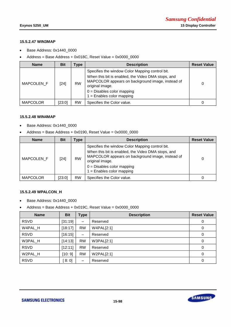
Samsung Confidential Exynos 5250_UM 15 Display Controller
15-98
15.5.2.47 WIN3MAP
Base Address: 0x1440_0000
Address = Base Address + 0x018C, Reset Value = 0x0000_0000
Name Bit Type Description Reset Value
MAPCOLEN_F [24] RW
Specifies the window Color Mapping control bit.
When this bit is enabled, the Video DMA stops, and
MAPCOLOR appears on background image, instead of
original image.
0 = Disables color mapping
1 = Enables color mapping
0
MAPCOLOR [23:0] RW Specifies the Color value. 0
15.5.2.48 WIN4MAP
Base Address: 0x1440_0000
Address = Base Address + 0x0190, Reset Value = 0x0000_0000
Name Bit Type Description Reset Value
MAPCOLEN_F [24] RW
Specifies the window Color Mapping control bit.
When this bit is enabled, the Video DMA stops, and
MAPCOLOR appears on background image, instead of
original image.
0 = Disables color mapping
1 = Enables color mapping
0
MAPCOLOR [23:0] RW Specifies the Color value. 0
15.5.2.49 WPALCON_H
Base Address: 0x1440_0000
Address = Base Address + 0x019C, Reset Value = 0x0000_0000
Name Bit Type Description Reset Value
RSVD [31:19] – Reserved 0
W4PAL_H [18:17] RW W4PAL[2:1] 0
RSVD [16:15] – Reserved 0
W3PAL_H [14:13] RW W3PAL[2:1] 0
RSVD [12:11] RW Reserved 0
W2PAL_H [10: 9] RW W2PAL[2:1] 0
RSVD [ 8: 0] – Reserved 0
Samsung Confidential Exynos 5250_UM 15 Display Controller
15-99
15.5.2.50 WPALCON_L
Base Address: 0x1440_0000
Address = Base Address + 0x01A0, Reset Value = 0x0000_0000
Name Bit Type Description Reset Value
RSVD [31:10] – Reserved 0
PALUPDATEEN [9] RW 0 = Normal Mode
1 = Enables palette update 0
W4PAL_L [8] RW W4PAL[0] 0
W3PAL_L [7] RW W3PAL[0] 0
W2PAL_L [6] RW W2PAL[0] 0
W1PAL_L [ 5: 3] RW W1PAL[2:0] 0
W0PAL_L [ 2: 0] RW W0PAL[2:0] 0
NOTE: WPALCON = {WPALCON_H, WPALCON_L}
WPALCON Description Reset Value
PALUPDATEEN 0 = Normal Mode
1 = Enable (Palette Update) 0
W4PAL[3:0]
Specifies the Window 4 Palette data format size.
000 = 16-bit (5:6:5)
001 = 16-bit (A:5:5:5)
010 = 18-bit (6:6:6)
011 = 18-bit (A:6:6:5)
100 = 19-bit (A:6:6:6)
101 = 24-bit (8:8:8)
110 = 25-bit (A:8:8:8)
111 = 32-bit (8:8:8:8) (A: 8-bit)
0
W3PAL[2:0]
Specifies the Window 3 Pallet data format size.
000 = 16-bit (5:6:5)
001 = 16-bit (A:5:5:5)
010 = 18-bit (6:6:6)
011 = 18-bit (A:6:6:5)
100 = 19-bit (A:6:6:6)
101 = 24-bit (8:8:8)
110 = 25-bit (A:8:8:8)
111 = 32-bit (8:8:8:8) (A: 8-bit)
0
W2PAL[2:0]
Specifies the Window 2 Pallet data format size.
000 = 16-bit (5:6:5)
001 = 16-bit (A:5:5:5)
010 = 18-bit (6:6:6)
011 = 18-bit (A:6:6:5)
100 = 19-bit (A:6:6:6)
101 = 24-bit (8:8:8)
110 = 25-bit (A:8:8:8)
111 = 32-bit (8:8:8:8) (A: 8-bit)
0
Samsung Confidential Exynos 5250_UM 15 Display Controller
15-100
WPALCON Description Reset Value
W1PAL[2:0]
Specifies the Window 1 Pallet data format size.
000 = 25-bit (A:8:8:8)
001 = 24-bit (8:8:8)
010 = 19-bit (A:6:6:6)
011 = 18-bit (A:6:6:5)
100 = 18-bit (6:6:6)
101 = 16-bit (A:5:5:5)
110 = 16-bit (5:6:5)
111 = 32-bit (8:8:8:8) (A: 8-bit)
0
W0PAL[2:0]
Specifies the Window 0 pallet data format size.
000 = 25-bit (A:8:8:8)
001 = 24-bit (8:8:8)
010 = 19-bit (A:6:6:6)
011 = 18-bit (A:6:6:5)
100 = 18-bit (6:6:6)
101 = 16-bit (A:5:5:5)
110 = 16-bit (5:6:5)
111 = 32-bit (8:8:8:8) (A: 8-bit)
0
NOTE: The bit map for W0/W1 and W2/W3/W4 is different.

Samsung Confidential Exynos 5250_UM 15 Display Controller
15-101
15.5.2.51 LAYERSYNC_CON
Base Address: 0x1440_0000
Address = Base Address + 0x01C0, Reset Value = 0xFFFF_FF00
Name Bit Type Description Reset Value
FIRE_PULSE_WID
TH [31:8] RW Reserved 0xFF_FFFF
RSVD [7] – Reserved 0
SYNC_UPDATE [6] RS
All enabled layersync channel updated
0 = Do NOT update shadow register next frame
1 = Update shadow register next frame
0
ALL_SYNC_ON [5] RW
Enable all channel layersync
0 = Disable all channel layersync
1 = Enable all channel layersync
0
W4_SYNC_ON [4] RW
Enable channel 4’s layersync to display 3D image.
0 = Disable channel 4 layersync
1 = Enable channel 4 layersync
0
W3_SYNC_ON [3] RW
Enable channel 3’s layersync to display 3D image.
0 = Disable channel 3 layersync
1 = Enable channel 3 layersync
0
W2_SYNC_ON [2] RW
Enable channel 2’s layersync to display 3D image.
0 = Disable channel 2 layersync
1 = Enable channel 2 layersync
0
W1_SYNC_ON [1] RW
Enable channel 1’s layersync to display 3D image.
0 = Disable channel 1 layersync
1 = Enable channel 1 layersync
0
W0_SYNC_ON [0] RW
Enable channel 0’s layersync to display 3D image.
0 = Disable channel 0 layersync
1 = Enable channel 0 layersync
0
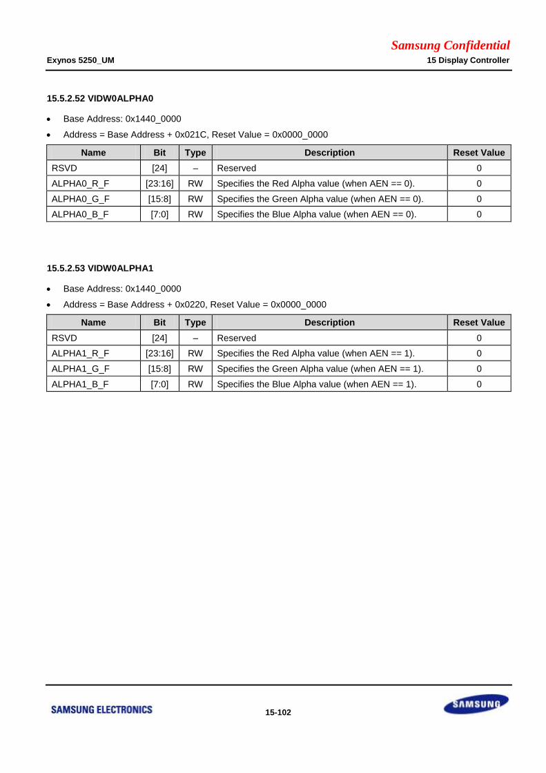
Samsung Confidential Exynos 5250_UM 15 Display Controller
15-102
15.5.2.52 VIDW0ALPHA0
Base Address: 0x1440_0000
Address = Base Address + 0x021C, Reset Value = 0x0000_0000
Name Bit Type Description Reset Value
RSVD [24] – Reserved 0
ALPHA0_R_F [23:16] RW Specifies the Red Alpha value (when AEN == 0). 0
ALPHA0_G_F [15:8] RW Specifies the Green Alpha value (when AEN == 0). 0
ALPHA0_B_F [7:0] RW Specifies the Blue Alpha value (when AEN == 0). 0
15.5.2.53 VIDW0ALPHA1
Base Address: 0x1440_0000
Address = Base Address + 0x0220, Reset Value = 0x0000_0000
Name Bit Type Description Reset Value
RSVD [24] – Reserved 0
ALPHA1_R_F [23:16] RW Specifies the Red Alpha value (when AEN == 1). 0
ALPHA1_G_F [15:8] RW Specifies the Green Alpha value (when AEN == 1). 0
ALPHA1_B_F [7:0] RW Specifies the Blue Alpha value (when AEN == 1). 0
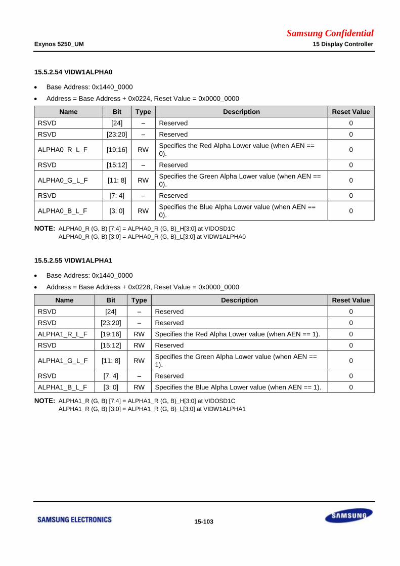
Samsung Confidential Exynos 5250_UM 15 Display Controller
15-103
15.5.2.54 VIDW1ALPHA0
Base Address: 0x1440_0000
Address = Base Address + 0x0224, Reset Value = 0x0000_0000
Name Bit Type Description Reset Value
RSVD [24] – Reserved 0
RSVD [23:20] – Reserved 0
ALPHA0_R_L_F [19:16] RW Specifies the Red Alpha Lower value (when AEN ==
0). 0
RSVD [15:12] – Reserved 0
ALPHA0_G_L_F [11: 8] RW Specifies the Green Alpha Lower value (when AEN ==
0). 0
RSVD [7: 4] – Reserved 0
ALPHA0_B_L_F [3: 0] RW Specifies the Blue Alpha Lower value (when AEN ==
0). 0
NOTE: ALPHA0_R (G, B) [7:4] = ALPHA0_R (G, B)_H[3:0] at VIDOSD1C
ALPHA0_R (G, B) [3:0] = ALPHA0_R (G, B)_L[3:0] at VIDW1ALPHA0
15.5.2.55 VIDW1ALPHA1
Base Address: 0x1440_0000
Address = Base Address + 0x0228, Reset Value = 0x0000_0000
Name Bit Type Description Reset Value
RSVD [24] – Reserved 0
RSVD [23:20] – Reserved 0
ALPHA1_R_L_F [19:16] RW Specifies the Red Alpha Lower value (when AEN == 1). 0
RSVD [15:12] RW Reserved 0
ALPHA1_G_L_F [11: 8] RW Specifies the Green Alpha Lower value (when AEN ==
1). 0
RSVD [7: 4] – Reserved 0
ALPHA1_B_L_F [3: 0] RW Specifies the Blue Alpha Lower value (when AEN == 1). 0
NOTE: ALPHA1_R (G, B) [7:4] = ALPHA1_R (G, B)_H[3:0] at VIDOSD1C
ALPHA1_R (G, B) [3:0] = ALPHA1_R (G, B)_L[3:0] at VIDW1ALPHA1
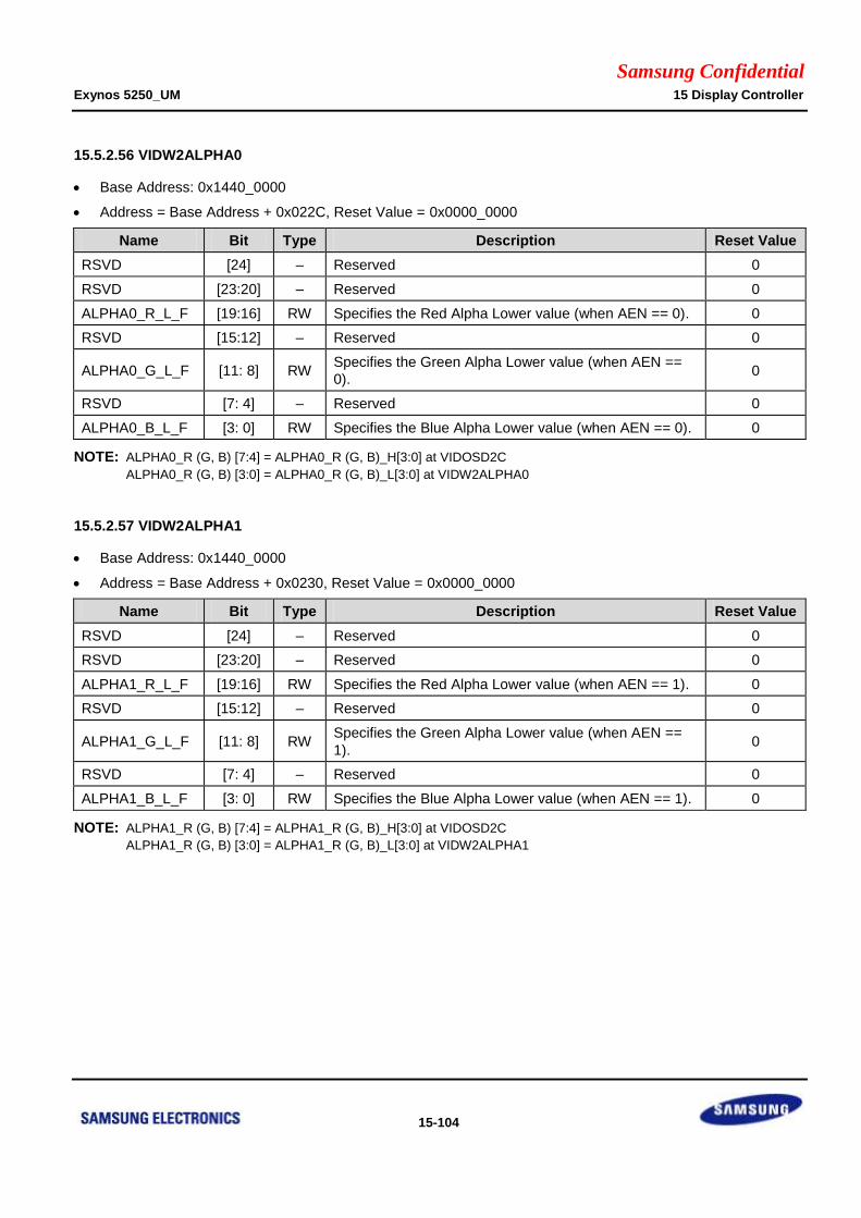
Samsung Confidential Exynos 5250_UM 15 Display Controller
15-104
15.5.2.56 VIDW2ALPHA0
Base Address: 0x1440_0000
Address = Base Address + 0x022C, Reset Value = 0x0000_0000
Name Bit Type Description Reset Value
RSVD [24] – Reserved 0
RSVD [23:20] – Reserved 0
ALPHA0_R_L_F [19:16] RW Specifies the Red Alpha Lower value (when AEN == 0). 0
RSVD [15:12] – Reserved 0
ALPHA0_G_L_F [11: 8] RW Specifies the Green Alpha Lower value (when AEN ==
0). 0
RSVD [7: 4] – Reserved 0
ALPHA0_B_L_F [3: 0] RW Specifies the Blue Alpha Lower value (when AEN == 0). 0
NOTE: ALPHA0_R (G, B) [7:4] = ALPHA0_R (G, B)_H[3:0] at VIDOSD2C
ALPHA0_R (G, B) [3:0] = ALPHA0_R (G, B)_L[3:0] at VIDW2ALPHA0
15.5.2.57 VIDW2ALPHA1
Base Address: 0x1440_0000
Address = Base Address + 0x0230, Reset Value = 0x0000_0000
Name Bit Type Description Reset Value
RSVD [24] – Reserved 0
RSVD [23:20] – Reserved 0
ALPHA1_R_L_F [19:16] RW Specifies the Red Alpha Lower value (when AEN == 1). 0
RSVD [15:12] – Reserved 0
ALPHA1_G_L_F [11: 8] RW Specifies the Green Alpha Lower value (when AEN ==
1). 0
RSVD [7: 4] – Reserved 0
ALPHA1_B_L_F [3: 0] RW Specifies the Blue Alpha Lower value (when AEN == 1). 0
NOTE: ALPHA1_R (G, B) [7:4] = ALPHA1_R (G, B)_H[3:0] at VIDOSD2C
ALPHA1_R (G, B) [3:0] = ALPHA1_R (G, B)_L[3:0] at VIDW2ALPHA1
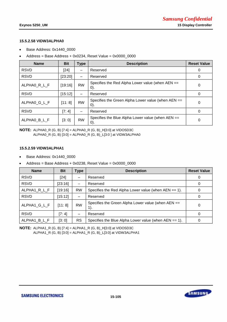
Samsung Confidential Exynos 5250_UM 15 Display Controller
15-105
15.5.2.58 VIDW3ALPHA0
Base Address: 0x1440_0000
Address = Base Address + 0x0234, Reset Value = 0x0000_0000
Name Bit Type Description Reset Value
RSVD [24] – Reserved 0
RSVD [23:20] – Reserved 0
ALPHA0_R_L_F [19:16] RW Specifies the Red Alpha Lower value (when AEN ==
0). 0
RSVD [15:12] – Reserved 0
ALPHA0_G_L_F [11: 8] RW Specifies the Green Alpha Lower value (when AEN ==
0). 0
RSVD [7: 4] – Reserved 0
ALPHA0_B_L_F [3: 0] RW Specifies the Blue Alpha Lower value (when AEN ==
0). 0
NOTE: ALPHA0_R (G, B) [7:4] = ALPHA0_R (G, B)_H[3:0] at VIDOSD3C
ALPHA0_R (G, B) [3:0] = ALPHA0_R (G, B)_L[3:0 ] at VIDW3ALPHA0
15.5.2.59 VIDW3ALPHA1
Base Address: 0x1440_0000
Address = Base Address + 0x0238, Reset Value = 0x0000_0000
Name Bit Type Description Reset Value
RSVD [24] – Reserved 0
RSVD [23:16] – Reserved 0
ALPHA1_R_L_F [19:16] RW Specifies the Red Alpha Lower value (when AEN == 1). 0
RSVD [15:12] – Reserved 0
ALPHA1_G_L_F [11: 8] RW Specifies the Green Alpha Lower value (when AEN ==
1). 0
RSVD [7: 4] – Reserved 0
ALPHA1_B_L_F [3: 0] RS Specifies the Blue Alpha Lower value (when AEN == 1). 0
NOTE: ALPHA1_R (G, B) [7:4] = ALPHA1_R (G, B)_H[3:0] at VIDOSD3C
ALPHA1_R (G, B) [3:0] = ALPHA1_R (G, B)_L[3:0] at VIDW3ALPHA1

Samsung Confidential Exynos 5250_UM 15 Display Controller
15-106
15.5.2.60 VIDW4ALPHA0
Base Address: 0x1440_0000
Address = Base Address + 0x023C, Reset Value = 0x0000_0000
Name Bit Type Description Reset Value
RSVD [24] – Reserved 0
RSVD [23:20] – Reserved 0
ALPHA0_R_L_F [19:16] RW Specifies the Red Alpha Lower value (when AEN == 0). 0
RSVD [15:12] – Reserved 0
ALPHA0_G_L_F [11: 8] RW Specifies the Green Alpha Lower value (when AEN ==
0). 0
RSVD [7: 4] – Reserved 0
ALPHA0_B_L_F [3: 0] RW Specifies the Blue Alpha Lower value (when AEN == 0). 0
NOTE: ALPHA0_R (G, B) [7:4] = ALPHA0_R (G, B)_H[3:0] at VIDOSD4C
ALPHA0_R (G, B) [3:0] = ALPHA0_R (G, B)_L[3:0] at VIDW4ALPHA0
15.5.2.61 VIDW4ALPHA1
Base Address: 0x1440_0000
Address = Base Address + 0x0240, Reset Value = 0x0000_0000
Name Bit Type Description Reset Value
RSVD [24] – Reserved 0
RSVD [23:20] – Reserved 0
ALPHA1_R_L_F [19:16] RW Specifies the Red Alpha Lower value (when AEN == 1). 0
RSVD [15:12] – Reserved 0
ALPHA1_G_L_F [11: 8] RW Specifies the Green Alpha Lower value (when AEN ==
1). 0
RSVD [7: 4] – Reserved 0
ALPHA1_B_L_F [3: 0] RW Specifies the Blue Alpha Lower value (when AEN == 1). 0
NOTE: ALPHA1_R (G, B) [7:4] = ALPHA1_R (G, B)_H[3:0] at VIDOSD4C
ALPHA1_R (G, B) [3:0] = ALPHA1_R (G, B)_L[3:0] at VIDW4ALPHA1
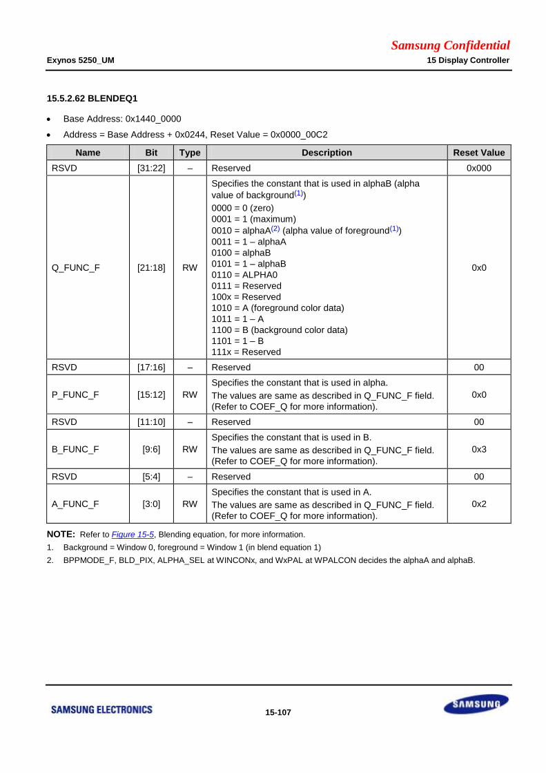
Samsung Confidential Exynos 5250_UM 15 Display Controller
15-107
15.5.2.62 BLENDEQ1
Base Address: 0x1440_0000
Address = Base Address + 0x0244, Reset Value = 0x0000_00C2
Name Bit Type Description Reset Value
RSVD [31:22] – Reserved 0x000
Q_FUNC_F [21:18] RW
Specifies the constant that is used in alphaB (alpha
value of background(1))
0000 = 0 (zero)
0001 = 1 (maximum)
0010 = alphaA(2) (alpha value of foreground(1))
0011 = 1 – alphaA
0100 = alphaB
0101 = 1 – alphaB
0110 = ALPHA0
0111 = Reserved
100x = Reserved
1010 = A (foreground color data)
1011 = 1 – A
1100 = B (background color data)
1101 = 1 – B
111x = Reserved
0x0
RSVD [17:16] – Reserved 00
P_FUNC_F [15:12] RW
Specifies the constant that is used in alpha.
The values are same as described in Q_FUNC_F field.
(Refer to COEF_Q for more information).
0x0
RSVD [11:10] – Reserved 00
B_FUNC_F [9:6] RW
Specifies the constant that is used in B.
The values are same as described in Q_FUNC_F field.
(Refer to COEF_Q for more information).
0x3
RSVD [5:4] – Reserved 00
A_FUNC_F [3:0] RW
Specifies the constant that is used in A.
The values are same as described in Q_FUNC_F field.
(Refer to COEF_Q for more information).
0x2
NOTE: Refer to Figure 15-5, Blending equation, for more information.
1. Background = Window 0, foreground = Window 1 (in blend equation 1)
2. BPPMODE_F, BLD_PIX, ALPHA_SEL at WINCONx, and WxPAL at WPALCON decides the alphaA and alphaB.
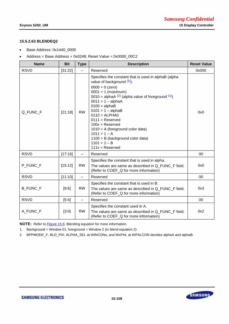
Samsung Confidential Exynos 5250_UM 15 Display Controller
15-108
15.5.2.63 BLENDEQ2
Base Address: 0x1440_0000
Address = Base Address + 0x0248, Reset Value = 0x0000_00C2
Name Bit Type Description Reset Value
RSVD [31:22] – Reserved 0x000
Q_FUNC_F [21:18] RW
Specifies the constant that is used in alphaB (alpha
value of background (1)).
0000 = 0 (zero)
0001 = 1 (maximum)
0010 = alphaA (2) (alpha value of foreground (1))
0011 = 1 – alphaA
0100 = alphaB
0101 = 1 – alphaB
0110 = ALPHA0
0111 = Reserved
100x = Reserved
1010 = A (foreground color data)
1011 = 1 – A
1100 = B (background color data)
1101 = 1 – B
111x = Reserved
0x0
RSVD [17:16] – Reserved 00
P_FUNC_F [15:12] RW
Specifies the constant that is used in alpha.
The values are same as described in Q_FUNC_F field.
(Refer to COEF_Q for more information)
0x0
RSVD [11:10] – Reserved 00
B_FUNC_F [9:6] RW
Specifies the constant that is used in B.
The values are same as described in Q_FUNC_F field.
(Refer to COEF_Q for more information)
0x3
RSVD [5:4] – Reserved 00
A_FUNC_F [3:0] RW
Specifies the constant used in A.
The values are same as described in Q_FUNC_F field.
(Refer to COEF_Q for more information)
0x2
NOTE: Refer to Figure 15-5, Blending equation for more information.
1. Background = Window 01, foreground = Window 2 (in blend equation 2)
2. BPPMODE_F, BLD_PIX, ALPHA_SEL at WINCONx, and WxPAL at WPALCON decides alphaA and alphaB.
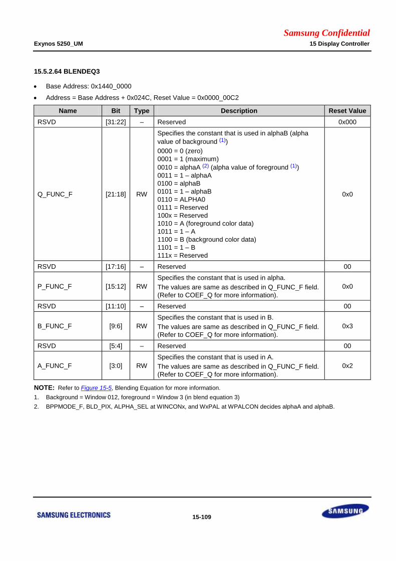
Samsung Confidential Exynos 5250_UM 15 Display Controller
15-109
15.5.2.64 BLENDEQ3
Base Address: 0x1440_0000
Address = Base Address + 0x024C, Reset Value = 0x0000_00C2
Name Bit Type Description Reset Value
RSVD [31:22] – Reserved 0x000
Q_FUNC_F [21:18] RW
Specifies the constant that is used in alphaB (alpha
value of background (1))
0000 = 0 (zero)
0001 = 1 (maximum)
0010 = alphaA (2) (alpha value of foreground (1))
0011 = 1 – alphaA
0100 = alphaB
0101 = 1 – alphaB
0110 = ALPHA0
0111 = Reserved
100x = Reserved
1010 = A (foreground color data)
1011 = 1 – A
1100 = B (background color data)
1101 = 1 – B
111x = Reserved
0x0
RSVD [17:16] – Reserved 00
P_FUNC_F [15:12] RW
Specifies the constant that is used in alpha.
The values are same as described in Q_FUNC_F field.
(Refer to COEF_Q for more information).
0x0
RSVD [11:10] – Reserved 00
B_FUNC_F [9:6] RW
Specifies the constant that is used in B.
The values are same as described in Q_FUNC_F field.
(Refer to COEF_Q for more information).
0x3
RSVD [5:4] – Reserved 00
A_FUNC_F [3:0] RW
Specifies the constant that is used in A.
The values are same as described in Q_FUNC_F field.
(Refer to COEF_Q for more information).
0x2
NOTE: Refer to Figure 15-5, Blending Equation for more information.
1. Background = Window 012, foreground = Window 3 (in blend equation 3)
2. BPPMODE_F, BLD_PIX, ALPHA_SEL at WINCONx, and WxPAL at WPALCON decides alphaA and alphaB.

Samsung Confidential Exynos 5250_UM 15 Display Controller
15-110
15.5.2.65 BLENDEQ4
Base Address: 0x1440_0000
Address = Base Address + 0x0250, Reset Value = 0x0000_00C2
Name Bit Type Description Reset Value
RSVD [31:22] – Reserved 0x000
Q_FUNC_F [21:18] RW
Specifies the constant that is used in alphaB (alpha
value of background (1))
0000 = 0 (zero)
0001 = 1 (maximum)
0010 = alphaA (2) (alpha value of foreground (1))
0011 = 1 – alphaA
0100 = alphaB
0101 = 1 – alphaB
0110 = ALPHA0
0111 = Reserved
100x = Reserved
1010 = A (foreground color data)
1011 = 1 – A
1100 = B (background color data)
1101 = 1 – B
111x = Reserved
0x0
RSVD [17:16] – Reserved 00
P_FUNC_F [15:12] RW
Specifies the constant that is used in alpha.
The values are same as described in Q_FUNC_F field.
(Refer to COEF_Q for more information).
0x0
RSVD [11:10] – Reserved 00
B_FUNC_F [9:6] RW
Specifies the constant that is used in B.
The values are same as described in Q_FUNC_F field.
(Refer to COEF_Q for more information).
0x3
RSVD [5:4] – Reserved 00
A_FUNC_F [3:0] RW
Specifies the constant that is used in A.
The values are same as described in Q_FUNC_F field.
(Refer to COEF_Q for more information).
0x2
NOTE: Refer to Figure 15-5, Blending equation, for more information.
1. Background = Window 0123, foreground = Window 4 (in blend equation 4)
2. BPPMODE_F, BLD_PIX, ALPHA_SEL at WINCONx, and WxPAL at WPALCON decides alphaA and alphaB.
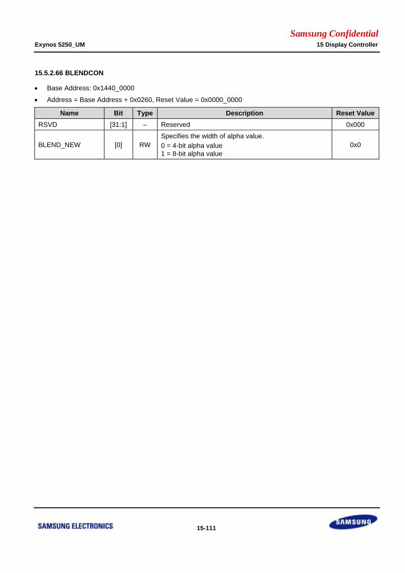
Samsung Confidential Exynos 5250_UM 15 Display Controller
15-111
15.5.2.66 BLENDCON
Base Address: 0x1440_0000
Address = Base Address + 0x0260, Reset Value = 0x0000_0000
Name Bit Type Description Reset Value
RSVD [31:1] – Reserved 0x000
BLEND_NEW [0] RW
Specifies the width of alpha value.
0 = 4-bit alpha value
1 = 8-bit alpha value
0x0

Samsung Confidential Exynos 5250_UM 15 Display Controller
15-112
15.5.2.67 W013DSTERECON
Base Address: 0x1440_0000
Address = Base Address + 0x0254, Reset Value = 0x0000_0000
Name Bit Type Description Reset Value
RSVD [31:19] – Reserved 0
WIDTH [18:7] RW Specifies the Width of frame image. WIDTH = image width
– 1 0
MERGE_EN [6] RW Specifies the enable signal for Left frame and Right frame
merging block. 0
A_L_FIRST [5] RW Specifies the Left First signal for Alpha data. 0
R_L_FIRST [4] RW Specifies the Left First signal for Red data. 0
G_L_FIRST [3] RW Specifies the Left First signal for Green data. 0
B_L_FIRST [2] RW Specifies the Left First signal for Blue data. 0
INTERPOL_EN [1] RW Specifies the Interpolation enable signal. 0
LINE_SWAP [0] RW Specifies the Line Swapping enable signal. 0
15.5.2.68 W233DSTEREOCON
Base Address: 0x1440_0000
Address = Base Address + 0x0258, Reset Value = 0x0000_0000
Name Bit Type Description Reset Value
RSVD [31:19] – Reserved 0
WIDTH [18:7] RW Specifies the Width of frame image.
WIDTH = image width – 1 0
MERGE_EN [6] RW Specifies the enable signal for L frame and R frame
merging block. 0
A_L_FIRST [5] RW Specifies the Left First signal for Alpha data. 0
R_L_FIRST [4] RW Specifies the Left First signal for Red data. 0
G_L_FIRST [3] RW Specifies the Left First signal for Green data. 0
B_L_FIRST [2] RW Specifies the Left First signal for Blue data. 0
INTERPOL_EN [1] RW Specifies the Interpolation enable signal. 0
LINE_SWAP [0] RW Specifies the Line Swapping enable signal. 0
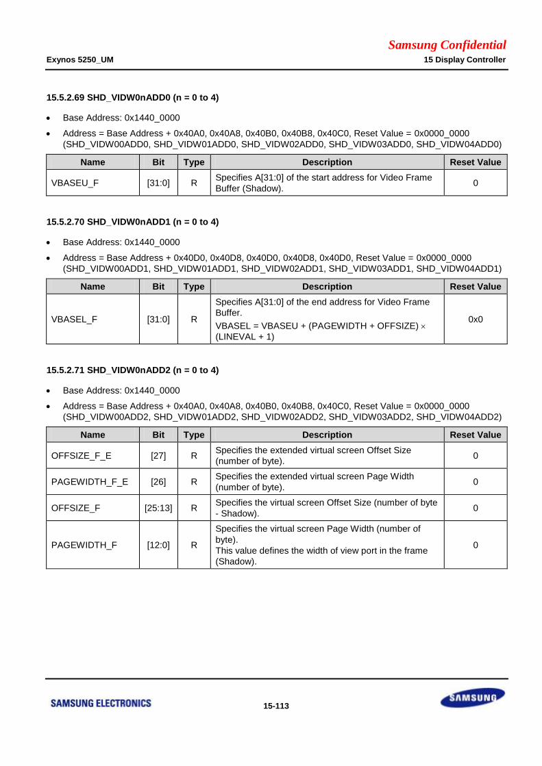
Samsung Confidential Exynos 5250_UM 15 Display Controller
15-113
15.5.2.69 SHD_VIDW0nADD0 (n = 0 to 4)
Base Address: 0x1440_0000
Address = Base Address + 0x40A0, 0x40A8, 0x40B0, 0x40B8, 0x40C0, Reset Value = 0x0000_0000
(SHD_VIDW00ADD0, SHD_VIDW01ADD0, SHD_VIDW02ADD0, SHD_VIDW03ADD0, SHD_VIDW04ADD0)
Name Bit Type Description Reset Value
VBASEU_F [31:0] R Specifies A[31:0] of the start address for Video Frame
Buffer (Shadow). 0
15.5.2.70 SHD_VIDW0nADD1 (n = 0 to 4)
Base Address: 0x1440_0000
Address = Base Address + 0x40D0, 0x40D8, 0x40D0, 0x40D8, 0x40D0, Reset Value = 0x0000_0000
(SHD_VIDW00ADD1, SHD_VIDW01ADD1, SHD_VIDW02ADD1, SHD_VIDW03ADD1, SHD_VIDW04ADD1)
Name Bit Type Description Reset Value
VBASEL_F [31:0] R
Specifies A[31:0] of the end address for Video Frame
Buffer.
VBASEL = VBASEU + (PAGEWIDTH + OFFSIZE)
(LINEVAL + 1)
0x0
15.5.2.71 SHD_VIDW0nADD2 (n = 0 to 4)
Base Address: 0x1440_0000
Address = Base Address + 0x40A0, 0x40A8, 0x40B0, 0x40B8, 0x40C0, Reset Value = 0x0000_0000
(SHD_VIDW00ADD2, SHD_VIDW01ADD2, SHD_VIDW02ADD2, SHD_VIDW03ADD2, SHD_VIDW04ADD2)
Name Bit Type Description Reset Value
OFFSIZE_F_E [27] R Specifies the extended virtual screen Offset Size
(number of byte). 0
PAGEWIDTH_F_E [26] R Specifies the extended virtual screen Page Width
(number of byte). 0
OFFSIZE_F [25:13] R Specifies the virtual screen Offset Size (number of byte
- Shadow). 0
PAGEWIDTH_F [12:0] R
Specifies the virtual screen Page Width (number of
byte).
This value defines the width of view port in the frame
(Shadow).
0
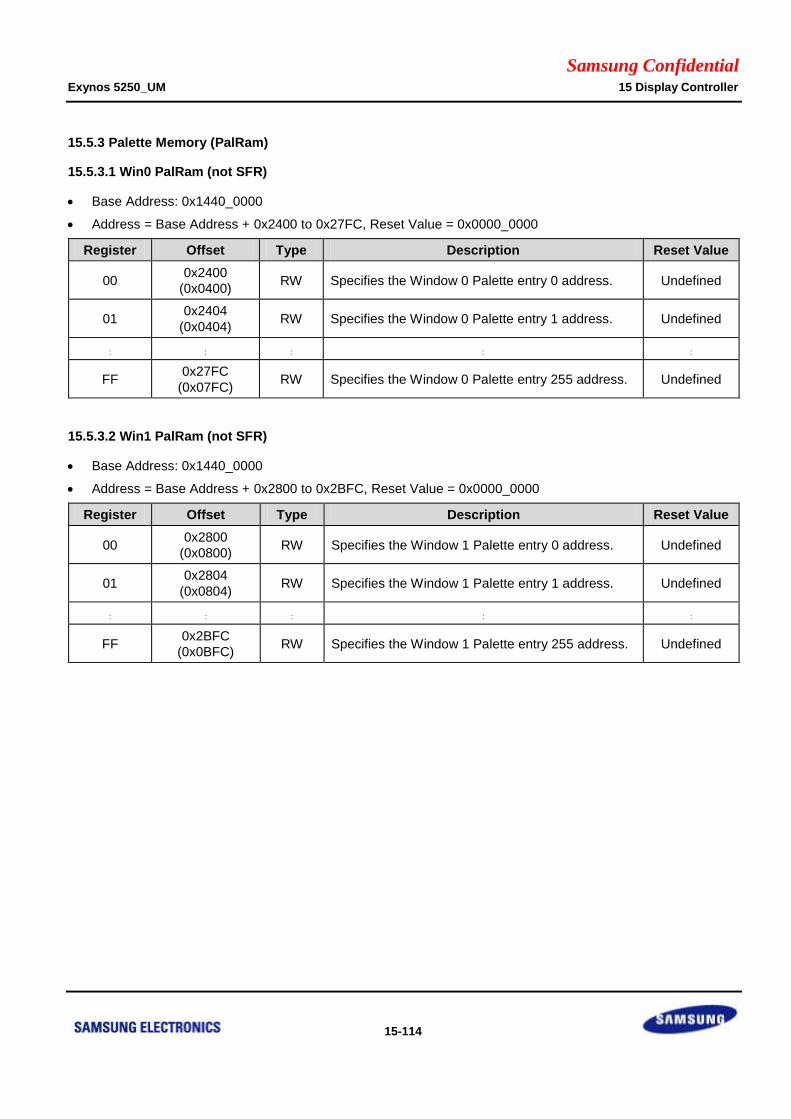
Samsung Confidential Exynos 5250_UM 15 Display Controller
15-114
15.5.3 Palette Memory (PalRam)
15.5.3.1 Win0 PalRam (not SFR)
Base Address: 0x1440_0000
Address = Base Address + 0x2400 to 0x27FC, Reset Value = 0x0000_0000
Register Offset Type Description Reset Value
00 0x2400
(0x0400) RW Specifies the Window 0 Palette entry 0 address. Undefined
01 0x2404
(0x0404) RW Specifies the Window 0 Palette entry 1 address. Undefined
: : : : :
FF 0x27FC
(0x07FC) RW Specifies the Window 0 Palette entry 255 address. Undefined
15.5.3.2 Win1 PalRam (not SFR)
Base Address: 0x1440_0000
Address = Base Address + 0x2800 to 0x2BFC, Reset Value = 0x0000_0000
Register Offset Type Description Reset Value
00 0x2800
(0x0800) RW Specifies the Window 1 Palette entry 0 address. Undefined
01 0x2804
(0x0804) RW Specifies the Window 1 Palette entry 1 address. Undefined
: : : : :
FF 0x2BFC
(0x0BFC) RW Specifies the Window 1 Palette entry 255 address. Undefined
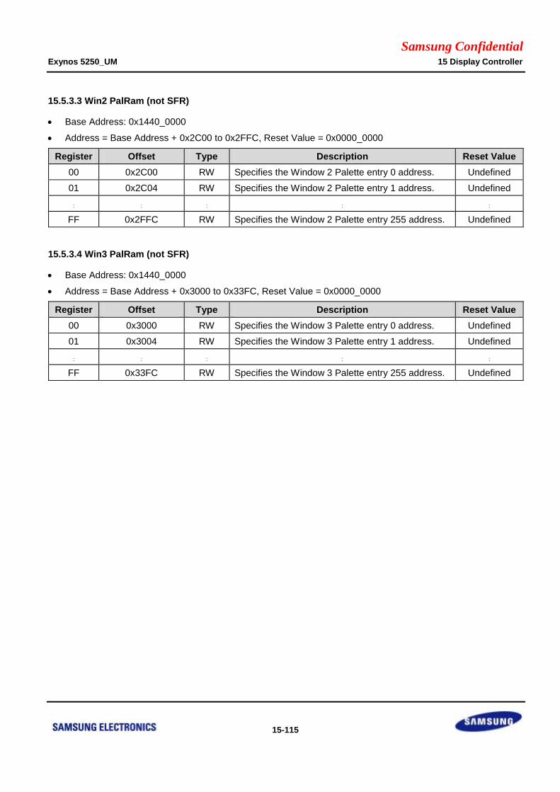
Samsung Confidential Exynos 5250_UM 15 Display Controller
15-115
15.5.3.3 Win2 PalRam (not SFR)
Base Address: 0x1440_0000
Address = Base Address + 0x2C00 to 0x2FFC, Reset Value = 0x0000_0000
Register Offset Type Description Reset Value
00 0x2C00 RW Specifies the Window 2 Palette entry 0 address. Undefined
01 0x2C04 RW Specifies the Window 2 Palette entry 1 address. Undefined
: : : : :
FF 0x2FFC RW Specifies the Window 2 Palette entry 255 address. Undefined
15.5.3.4 Win3 PalRam (not SFR)
Base Address: 0x1440_0000
Address = Base Address + 0x3000 to 0x33FC, Reset Value = 0x0000_0000
Register Offset Type Description Reset Value
00 0x3000 RW Specifies the Window 3 Palette entry 0 address. Undefined
01 0x3004 RW Specifies the Window 3 Palette entry 1 address. Undefined
: : : : :
FF 0x33FC RW Specifies the Window 3 Palette entry 255 address. Undefined
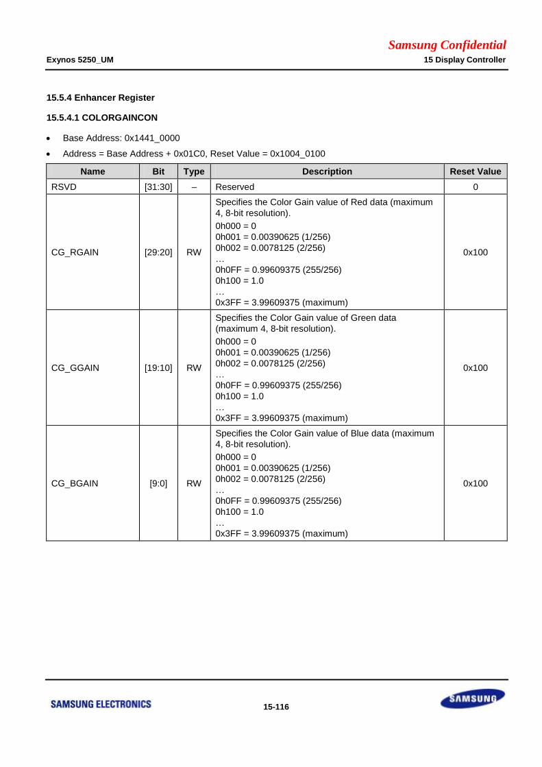
Samsung Confidential Exynos 5250_UM 15 Display Controller
15-116
15.5.4 Enhancer Register
15.5.4.1 COLORGAINCON
Base Address: 0x1441_0000
Address = Base Address + 0x01C0, Reset Value = 0x1004_0100
Name Bit Type Description Reset Value
RSVD [31:30] – Reserved 0
CG_RGAIN [29:20] RW
Specifies the Color Gain value of Red data (maximum
4, 8-bit resolution).
0h000 = 0
0h001 = 0.00390625 (1/256)
0h002 = 0.0078125 (2/256)
…
0h0FF = 0.99609375 (255/256)
0h100 = 1.0
…
0x3FF = 3.99609375 (maximum)
0x100
CG_GGAIN [19:10] RW
Specifies the Color Gain value of Green data
(maximum 4, 8-bit resolution).
0h000 = 0
0h001 = 0.00390625 (1/256)
0h002 = 0.0078125 (2/256)
…
0h0FF = 0.99609375 (255/256)
0h100 = 1.0
…
0x3FF = 3.99609375 (maximum)
0x100
CG_BGAIN [9:0] RW
Specifies the Color Gain value of Blue data (maximum
4, 8-bit resolution).
0h000 = 0
0h001 = 0.00390625 (1/256)
0h002 = 0.0078125 (2/256)
…
0h0FF = 0.99609375 (255/256)
0h100 = 1.0
…
0x3FF = 3.99609375 (maximum)
0x100
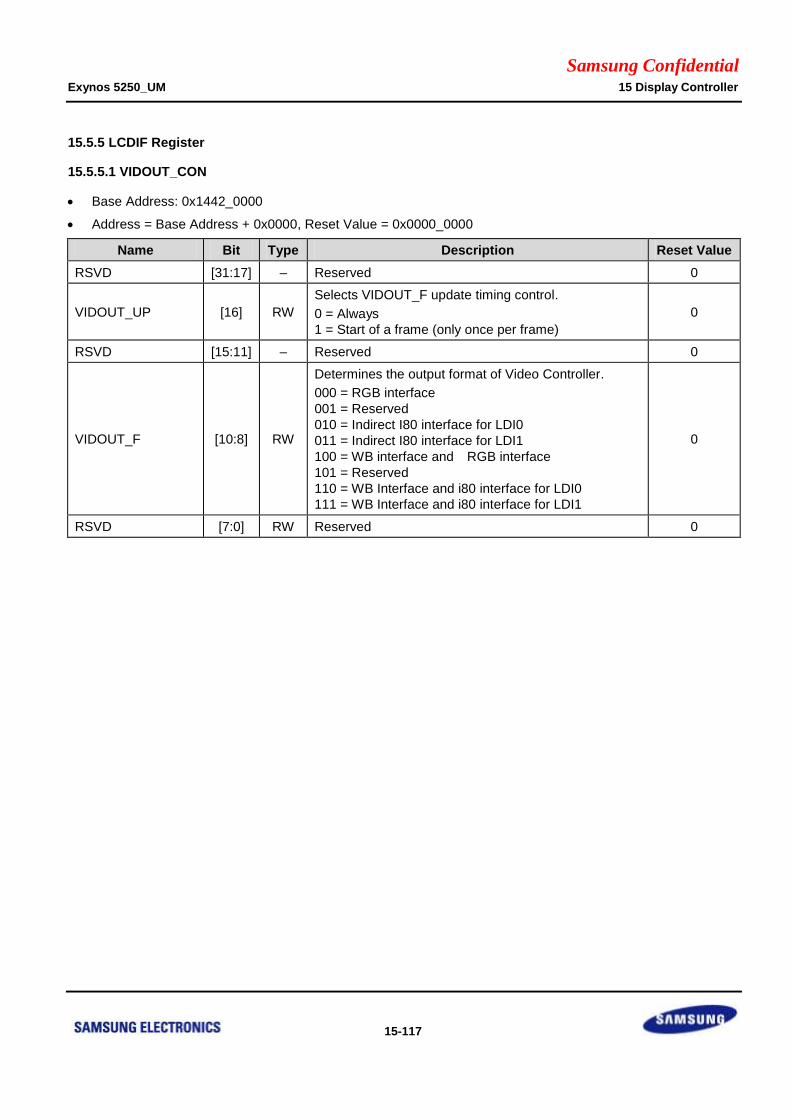
Samsung Confidential Exynos 5250_UM 15 Display Controller
15-117
15.5.5 LCDIF Register
15.5.5.1 VIDOUT_CON
Base Address: 0x1442_0000
Address = Base Address + 0x0000, Reset Value = 0x0000_0000
Name Bit Type Description Reset Value
RSVD [31:17] – Reserved 0
VIDOUT_UP [16] RW
Selects VIDOUT_F update timing control.
0 = Always
1 = Start of a frame (only once per frame)
0
RSVD [15:11] – Reserved 0
VIDOUT_F [10:8] RW
Determines the output format of Video Controller.
000 = RGB interface
001 = Reserved
010 = Indirect I80 interface for LDI0
011 = Indirect I80 interface for LDI1
100 = WB interface and RGB interface
101 = Reserved
110 = WB Interface and i80 interface for LDI0
111 = WB Interface and i80 interface for LDI1
0
RSVD [7:0] RW Reserved 0
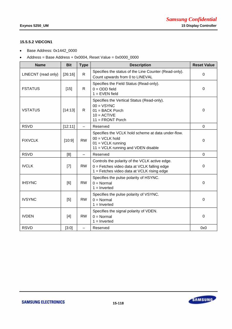
Samsung Confidential Exynos 5250_UM 15 Display Controller
15-118
15.5.5.2 VIDCON1
Base Address: 0x1442_0000
Address = Base Address + 0x0004, Reset Value = 0x0000_0000
Name Bit Type Description Reset Value
LINECNT (read only) [26:16] R Specifies the status of the Line Counter (Read-only).
Count upwards from 0 to LINEVAL 0
FSTATUS [15] R
Specifies the Field Status (Read-only).
0 = ODD field
1 = EVEN field
0
VSTATUS [14:13] R
Specifies the Vertical Status (Read-only).
00 = VSYNC
01 = BACK Porch
10 = ACTIVE
11 = FRONT Porch
0
RSVD [12:11] – Reserved 0
FIXVCLK [10:9] RW
Specifies the VCLK hold scheme at data under-flow.
00 = VCLK hold
01 = VCLK running
11 = VCLK running and VDEN disable
0
RSVD [8] – Reserved 0
IVCLK [7] RW
Controls the polarity of the VCLK active edge.
0 = Fetches video data at VCLK falling edge
1 = Fetches video data at VCLK rising edge
0
IHSYNC [6] RW
Specifies the pulse polarity of HSYNC.
0 = Normal
1 = Inverted
0
IVSYNC [5] RW
Specifies the pulse polarity of VSYNC.
0 = Normal
1 = Inverted
0
IVDEN [4] RW
Specifies the signal polarity of VDEN.
0 = Normal
1 = Inverted
0
RSVD [3:0] – Reserved 0x0
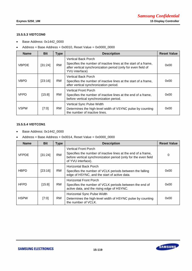
Samsung Confidential Exynos 5250_UM 15 Display Controller
15-119
15.5.5.3 VIDTCON0
Base Address: 0x1442_0000
Address = Base Address + 0x0010, Reset Value = 0x0000_0000
Name Bit Type Description Reset Value
VBPDE [31:24] RW
Vertical Back Porch
Specifies the number of inactive lines at the start of a frame,
after vertical synchronization period (only for even field of
YVU interface)
0x00
VBPD [23:16] RW
Vertical Back Porch
Specifies the number of inactive lines at the start of a frame,
after vertical synchronization period.
0x00
VFPD [15:8] RW
Vertical Front Porch
Specifies the number of inactive lines at the end of a frame,
before vertical synchronization period.
0x00
VSPW [7:0] RW
Vertical Sync Pulse Width
Determines the high-level width of VSYNC pulse by counting
the number of inactive lines.
0x00
15.5.5.4 VIDTCON1
Base Address: 0x1442_0000
Address = Base Address + 0x0014, Reset Value = 0x0000_0000
Name Bit Type Description Reset Value
VFPDE [31:24] RW
Vertical Front Porch
Specifies the number of inactive lines at the end of a frame,
before vertical synchronization period (only for the even field
of YVU interface).
0
HBPD [23:16] RW
Horizontal Back Porch
Specifies the number of VCLK periods between the falling
edge of HSYNC, and the start of active data.
0x00
HFPD [15:8] RW
Horizontal Front Porch
Specifies the number of VCLK periods between the end of
active data, and the rising edge of HSYNC.
0x00
HSPW [7:0] RW
Horizontal Sync Pulse Width
Determines the high-level width of HSYNC pulse by counting
the number of VCLK.
0x00
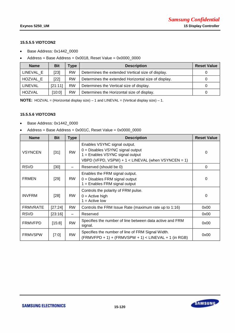
Samsung Confidential Exynos 5250_UM 15 Display Controller
15-120
15.5.5.5 VIDTCON2
Base Address: 0x1442_0000
Address = Base Address + 0x0018, Reset Value = 0x0000_0000
Name Bit Type Description Reset Value
LINEVAL_E [23] RW Determines the extended Vertical size of display. 0
HOZVAL_E [22] RW Determines the extended Horizontal size of display. 0
LINEVAL [21:11] RW Determines the Vertical size of display. 0
HOZVAL [10:0] RW Determines the Horizontal size of display. 0
NOTE: HOZVAL = (Horizontal display size) – 1 and LINEVAL = (Vertical display size) – 1.
15.5.5.6 VIDTCON3
Base Address: 0x1442_0000
Address = Base Address + 0x001C, Reset Value = 0x0000_0000
Name Bit Type Description Reset Value
VSYNCEN [31] RW
Enables VSYNC signal output.
0 = Disables VSYNC signal output
1 = Enables VSYNC signal output
VBPD (VFPD, VSPW) + 1 < LINEVAL (when VSYNCEN = 1)
0
RSVD [30] – Reserved (should be 0) 0
FRMEN [29] RW
Enables the FRM signal output.
0 = Disables FRM signal output
1 = Enables FRM signal output
0
INVFRM [28] RW
Controls the polarity of FRM pulse.
0 = Active high
1 = Active low
0
FRMVRATE [27:24] RW Controls the FRM Issue Rate (maximum rate up to 1:16) 0x00
RSVD [23:16] – Reserved 0x00
FRMVFPD [15:8] RW Specifies the number of line between data active and FRM
signal. 0x00
FRMVSPW [7:0] RW Specifies the number of line of FRM Signal Width.
(FRMVFPD + 1) + (FRMVSPW + 1) < LINEVAL + 1 (in RGB) 0x00
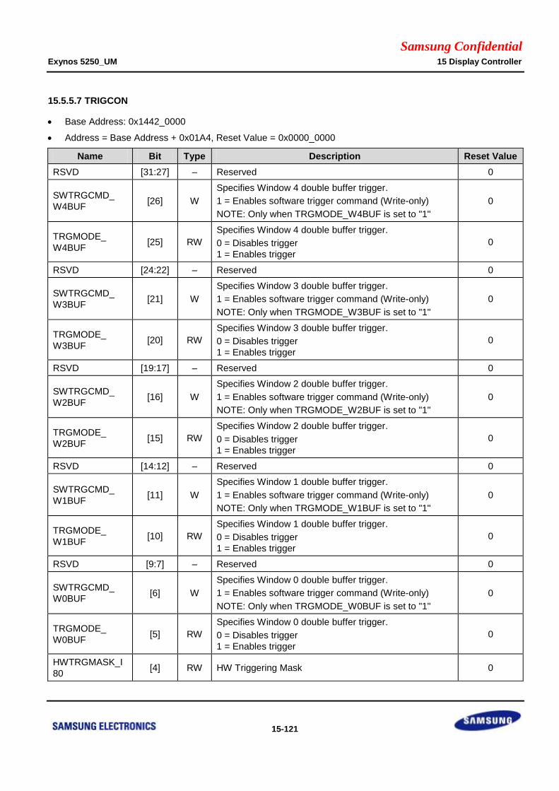
Samsung Confidential Exynos 5250_UM 15 Display Controller
15-121
15.5.5.7 TRIGCON
Base Address: 0x1442_0000
Address = Base Address + 0x01A4, Reset Value = 0x0000_0000
Name Bit Type Description Reset Value
RSVD [31:27] – Reserved 0
SWTRGCMD_
W4BUF [26] W
Specifies Window 4 double buffer trigger.
1 = Enables software trigger command (Write-only)
NOTE: Only when TRGMODE_W4BUF is set to "1"
0
TRGMODE_
W4BUF [25] RW
Specifies Window 4 double buffer trigger.
0 = Disables trigger
1 = Enables trigger
0
RSVD [24:22] – Reserved 0
SWTRGCMD_
W3BUF [21] W
Specifies Window 3 double buffer trigger.
1 = Enables software trigger command (Write-only)
NOTE: Only when TRGMODE_W3BUF is set to "1"
0
TRGMODE_
W3BUF [20] RW
Specifies Window 3 double buffer trigger.
0 = Disables trigger
1 = Enables trigger
0
RSVD [19:17] – Reserved 0
SWTRGCMD_
W2BUF [16] W
Specifies Window 2 double buffer trigger.
1 = Enables software trigger command (Write-only)
NOTE: Only when TRGMODE_W2BUF is set to "1"
0
TRGMODE_
W2BUF [15] RW
Specifies Window 2 double buffer trigger.
0 = Disables trigger
1 = Enables trigger
0
RSVD [14:12] – Reserved 0
SWTRGCMD_
W1BUF [11] W
Specifies Window 1 double buffer trigger.
1 = Enables software trigger command (Write-only)
NOTE: Only when TRGMODE_W1BUF is set to "1"
0
TRGMODE_
W1BUF [10] RW
Specifies Window 1 double buffer trigger.
0 = Disables trigger
1 = Enables trigger
0
RSVD [9:7] – Reserved 0
SWTRGCMD_
W0BUF [6] W
Specifies Window 0 double buffer trigger.
1 = Enables software trigger command (Write-only)
NOTE: Only when TRGMODE_W0BUF is set to "1"
0
TRGMODE_
W0BUF [5] RW
Specifies Window 0 double buffer trigger.
0 = Disables trigger
1 = Enables trigger
0
HWTRGMASK_I
80 [4] RW HW Triggering Mask 0
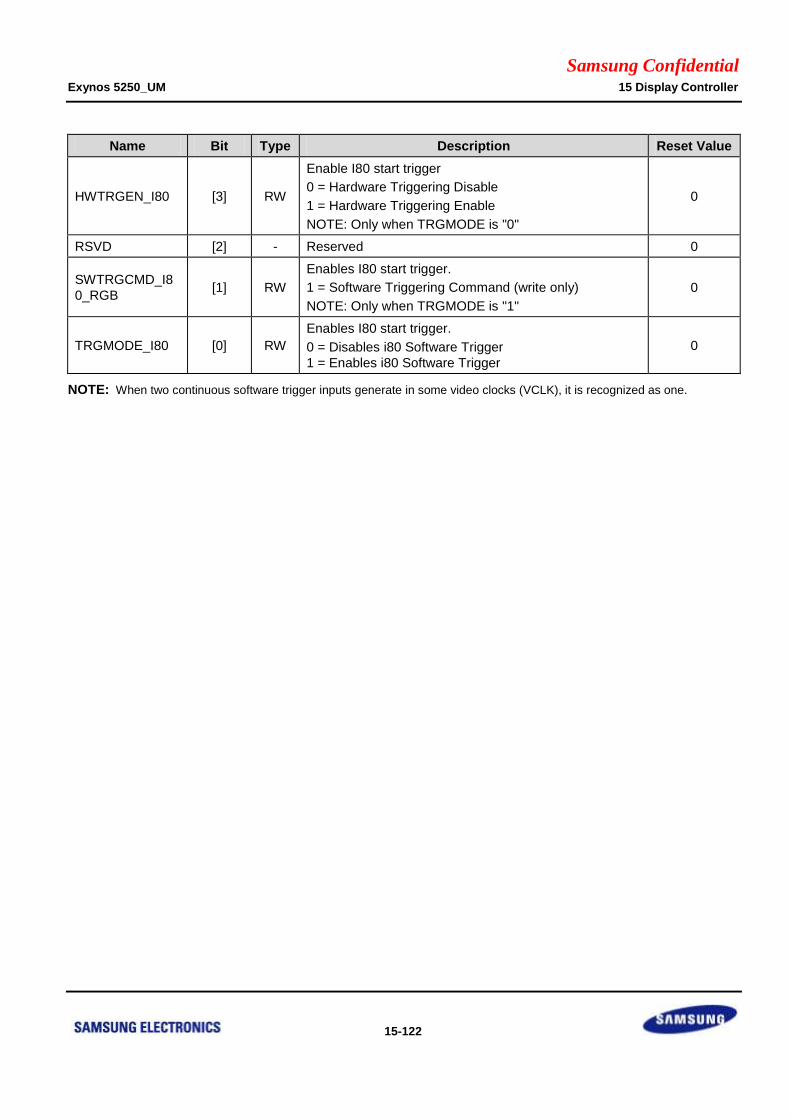
Samsung Confidential Exynos 5250_UM 15 Display Controller
15-122
Name Bit Type Description Reset Value
HWTRGEN_I80 [3] RW
Enable I80 start trigger
0 = Hardware Triggering Disable
1 = Hardware Triggering Enable
NOTE: Only when TRGMODE is "0"
0
RSVD [2] - Reserved 0
SWTRGCMD_I8
0_RGB [1] RW
Enables I80 start trigger.
1 = Software Triggering Command (write only)
NOTE: Only when TRGMODE is "1"
0
TRGMODE_I80 [0] RW
Enables I80 start trigger.
0 = Disables i80 Software Trigger
1 = Enables i80 Software Trigger
0
NOTE: When two continuous software trigger inputs generate in some video clocks (VCLK), it is recognized as one.
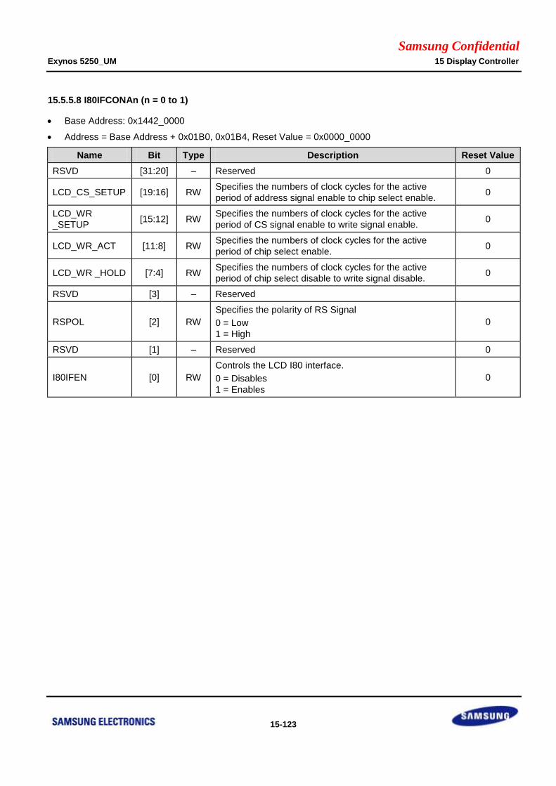
Samsung Confidential Exynos 5250_UM 15 Display Controller
15-123
15.5.5.8 I80IFCONAn (n = 0 to 1)
Base Address: 0x1442_0000
Address = Base Address + 0x01B0, 0x01B4, Reset Value = 0x0000_0000
Name Bit Type Description Reset Value
RSVD [31:20] – Reserved 0
LCD_CS_SETUP [19:16] RW Specifies the numbers of clock cycles for the active
period of address signal enable to chip select enable. 0
LCD_WR
_SETUP [15:12] RW
Specifies the numbers of clock cycles for the active
period of CS signal enable to write signal enable. 0
LCD_WR_ACT [11:8] RW Specifies the numbers of clock cycles for the active
period of chip select enable. 0
LCD_WR _HOLD [7:4] RW Specifies the numbers of clock cycles for the active
period of chip select disable to write signal disable. 0
RSVD [3] – Reserved
RSPOL [2] RW
Specifies the polarity of RS Signal
0 = Low
1 = High
0
RSVD [1] – Reserved 0
I80IFEN [0] RW
Controls the LCD I80 interface.
0 = Disables
1 = Enables
0
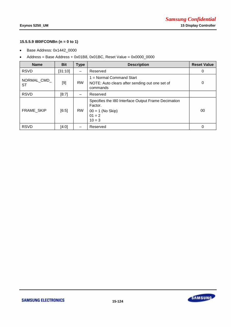
Samsung Confidential Exynos 5250_UM 15 Display Controller
15-124
15.5.5.9 I80IFCONBn (n = 0 to 1)
Base Address: 0x1442_0000
Address = Base Address + 0x01B8, 0x01BC, Reset Value = 0x0000_0000
Name Bit Type Description Reset Value
RSVD [31:10] – Reserved 0
NORMAL_CMD_
ST [9] RW
1 = Normal Command Start
NOTE: Auto clears after sending out one set of
commands
0
RSVD [8:7] – Reserved
FRAME_SKIP [6:5] RW
Specifies the I80 Interface Output Frame Decimation
Factor.
00 = 1 (No Skip)
01 = 2
10 = 3
00
RSVD [4:0] – Reserved 0

Samsung Confidential Exynos 5250_UM 15 Display Controller
15-125
15.5.5.10 LDI_CMDCON0
Base Address: 0x1442_0000
Address = Base Address + 0x01D0, Reset Value = 0x0000_0000
Name Bit Type Description Reset Value
RSVD [31:24] – Reserved
CMD11_EN [23:22] RW
00 = Disables
01 = Enables Normal Command
10 = Reserved
11 = Reserved
00
CMD10_EN [21:20] RW
00 = Disables
01 = Enables Normal Command
10 = Reserved
11 = Reserved
00
CMD9_EN [19:18] RW
00 = Disables
01 = Enables Normal Command
10 = Reserved
11 = Reserved
00
CMD8_EN [17:16] RW
00 = Disables
01 = Enables Normal Command
10 = Reserved
11 = Reserved
00
CMD7_EN [15:14] RW
00 = Disables
01 = Enables Normal Command
10 = Reserved
11 = Reserved
00
CMD6_EN [13:12] RW
00 = Disables
01 = Enables Normal Command
10 = Reserved
11 = Reserved
00
CMD5_EN [11:10] RW
00 = Disables
01 = Enables Normal Command
10 = Reserved
11 = Reserved
00
CMD4_EN [9:8] RW
00 = Disables
01 = Enables Normal Command
10 = Reserved
11 = Reserved
00
CMD3_EN [7:6] RW
00 = Disables
01 = Enables Normal Command
10 = Reserved
11 = Reserved
00
CMD2_EN [5:4] RW
00 = Disables
01 = Enables Normal Command
10 = Reserved
11 = Reserved
00
CMD1_EN [3:2] RW 00 = Disables 00

Samsung Confidential Exynos 5250_UM 15 Display Controller
15-126
Name Bit Type Description Reset Value
01 = Enables Normal Command
10 = Reserved
11 = Reserved
CMD0_EN [1:0] RW
00 = Disables
01 = Enables Normal Command
10 = Reserved
11 = Reserved
00
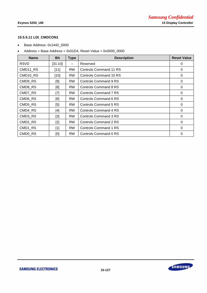
Samsung Confidential Exynos 5250_UM 15 Display Controller
15-127
15.5.5.11 LDI_CMDCON1
Base Address: 0x1442_0000
Address = Base Address + 0x01D4, Reset Value = 0x0000_0000
Name Bit Type Description Reset Value
RSVD [31:10] – Reserved 0
CMD11_RS [11] RW Controls Command 11 RS 0
CMD10_RS [10] RW Controls Command 10 RS 0
CMD9_RS [9] RW Controls Command 9 RS 0
CMD8_RS [8] RW Controls Command 8 RS 0
CMD7_RS [7] RW Controls Command 7 RS 0
CMD6_RS [6] RW Controls Command 6 RS 0
CMD5_RS [5] RW Controls Command 5 RS 0
CMD4_RS [4] RW Controls Command 4 RS 0
CMD3_RS [3] RW Controls Command 3 RS 0
CMD2_RS [2] RW Controls Command 2 RS 0
CMD1_RS [1] RW Controls Command 1 RS 0
CMD0_RS [0] RW Controls Command 0 RS 0
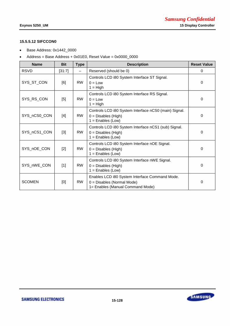
Samsung Confidential Exynos 5250_UM 15 Display Controller
15-128
15.5.5.12 SIFCCON0
Base Address: 0x1442_0000
Address = Base Address + 0x01E0, Reset Value = 0x0000_0000
Name Bit Type Description Reset Value
RSVD [31:7] – Reserved (should be 0) 0
SYS_ST_CON [6] RW
Controls LCD i80 System Interface ST Signal.
0 = Low
1 = High
0
SYS_RS_CON [5] RW
Controls LCD i80 System Interface RS Signal.
0 = Low
1 = High
0
SYS_nCS0_CON [4] RW
Controls LCD i80 System Interface nCS0 (main) Signal.
0 = Disables (High)
1 = Enables (Low)
0
SYS_nCS1_CON [3] RW
Controls LCD i80 System Interface nCS1 (sub) Signal.
0 = Disables (High)
1 = Enables (Low)
0
SYS_nOE_CON [2] RW
Controls LCD i80 System Interface nOE Signal.
0 = Disables (High)
1 = Enables (Low)
0
SYS_nWE_CON [1] RW
Controls LCD i80 System Interface nWE Signal.
0 = Disables (High)
1 = Enables (Low)
0
SCOMEN [0] RW
Enables LCD i80 System Interface Command Mode.
0 = Disables (Normal Mode)
1= Enables (Manual Command Mode)
0
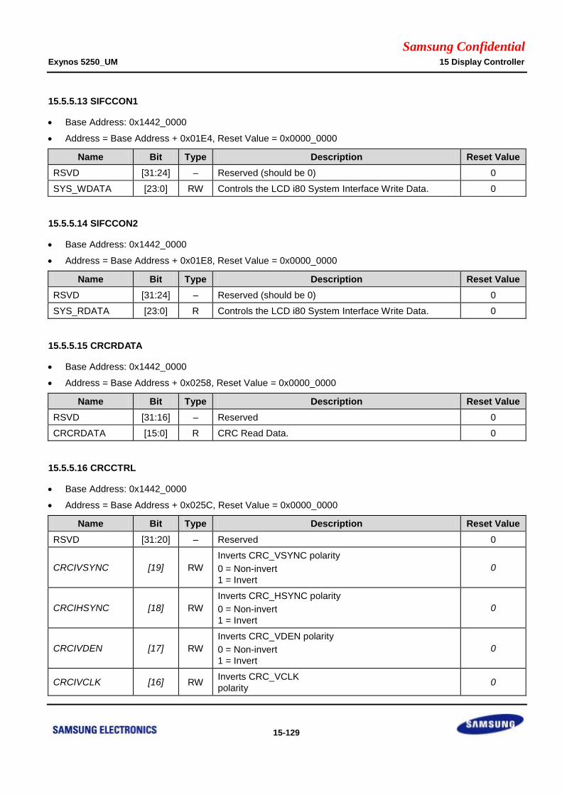
Samsung Confidential Exynos 5250_UM 15 Display Controller
15-129
15.5.5.13 SIFCCON1
Base Address: 0x1442_0000
Address = Base Address + 0x01E4, Reset Value = 0x0000_0000
Name Bit Type Description Reset Value
RSVD [31:24] – Reserved (should be 0) 0
SYS_WDATA [23:0] RW Controls the LCD i80 System Interface Write Data. 0
15.5.5.14 SIFCCON2
Base Address: 0x1442_0000
Address = Base Address + 0x01E8, Reset Value = 0x0000_0000
Name Bit Type Description Reset Value
RSVD [31:24] – Reserved (should be 0) 0
SYS_RDATA [23:0] R Controls the LCD i80 System Interface Write Data. 0
15.5.5.15 CRCRDATA
Base Address: 0x1442_0000
Address = Base Address + 0x0258, Reset Value = 0x0000_0000
Name Bit Type Description Reset Value
RSVD [31:16] – Reserved 0
CRCRDATA [15:0] R CRC Read Data. 0
15.5.5.16 CRCCTRL
Base Address: 0x1442_0000
Address = Base Address + 0x025C, Reset Value = 0x0000_0000
Name Bit Type Description Reset Value
RSVD [31:20] – Reserved 0
CRCIVSYNC [19] RW
Inverts CRC_VSYNC polarity
0 = Non-invert
1 = Invert
0
CRCIHSYNC [18] RW
Inverts CRC_HSYNC polarity
0 = Non-invert
1 = Invert
0
CRCIVDEN [17] RW
Inverts CRC_VDEN polarity
0 = Non-invert
1 = Invert
0
CRCIVCLK [16] RW Inverts CRC_VCLK
polarity 0
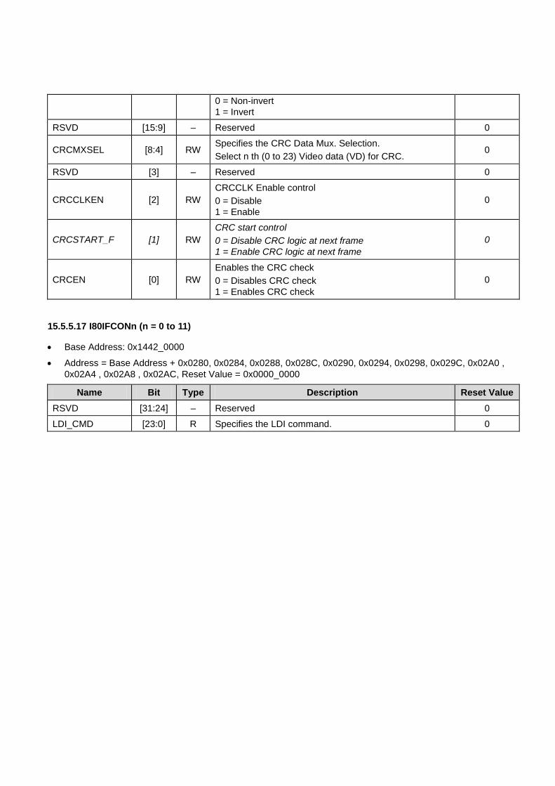
0 = Non-invert
1 = Invert
RSVD [15:9] – Reserved 0
CRCMXSEL [8:4] RW Specifies the CRC Data Mux. Selection.
Select n th (0 to 23) Video data (VD) for CRC. 0
RSVD [3] – Reserved 0
CRCCLKEN [2] RW
CRCCLK Enable control
0 = Disable
1 = Enable
0
CRCSTART_F [1] RW
CRC start control
0 = Disable CRC logic at next frame
1 = Enable CRC logic at next frame
0
CRCEN [0] RW
Enables the CRC check
0 = Disables CRC check
1 = Enables CRC check
0
15.5.5.17 I80IFCONn (n = 0 to 11)
Base Address: 0x1442_0000
Address = Base Address + 0x0280, 0x0284, 0x0288, 0x028C, 0x0290, 0x0294, 0x0298, 0x029C, 0x02A0 ,
0x02A4 , 0x02A8 , 0x02AC, Reset Value = 0x0000_0000
Name Bit Type Description Reset Value
RSVD [31:24] – Reserved 0
LDI_CMD [23:0] R Specifies the LDI command. 0
Samsung Confidential Exynos 5250_UM 16 Analog to Digital Converter (ADC)
16-1
16 Analog to Digital Converter (ADC)
This chapter describes the functions and usage of ADC
16.1 Overview
The 10-bit or 12-bit CMOS Analog to Digital Converter (ADC) comprises of 8-channel analog inputs. It converts
the analog input signal into 10-bit or 12-bit binary digital codes at a maximum conversion rate of 1MSPS with
5MHz A/D converter clock. A/D converter operates with on-chip sample-and-hold function. ADC supports low
power mode.
16.2 Features
The ADC includes the following features:
Resolution: 10-bit/12-bit (optional)
Differential Nonlinearity Error: 2.0 LSB (Max.)
Integral Nonlinearity Error: 4.0 LSB (Max.)
Maximum Conversion Rate: 1 MSPS
Low Power Consumption
Power Supply Voltage:1.8 V
Analog Input Range: 0 to 1.8 V
On-chip sample-and-hold function
Normal Conversion Mode
Waiting for Interrupt Mode

Samsung Confidential Exynos 5250_UM 16 Analog to Digital Converter (ADC)
16-2
16.3 ADC Interface Operation
16.3.1 Block Diagram ADC
Figure 16-1 is the functional block diagram of A/D converter.
ADC input
control
Interrupt
generation
Waiting for interrupt
VDDA_ADC
8:1
MUX
A/D
Converter
ADC
interface
INT_ADC0AIN0
AIN5
AIN4
AIN3
AIN2
AIN1
AIN6
AIN7
Figure 16-1 ADC Functional Block Diagram
Samsung Confidential Exynos 5250_UM 16 Analog to Digital Converter (ADC)
16-3
16.4 Function Descriptions
16.4.1 A/D Conversion Time
When the PCLK frequency is 66 MHz and the prescaler value is 65, total 12-bit conversion time is as follows.
A/D converter freq. = 66 MHz/(65 + 1) = 1 MHz
Conversion time = 1/(1 MHz/5 cycles) = 1/200 kHz = 5 s
NOTE: This A/D converter was designed to operate at maximum 5 MHz clock, so the conversion rate can go up to 1MSPS.
16.4.2 ADC conversion Mode
The operation of this mode is same as AIN0 to AIN7's. To initialize this mode, set the ADCCON (ADC control
register).
The converted data can be read out from ADCDATX (ADC conversion data X register).
16.4.3 Standby Mode
Standby mode is activated when STANDBY bit is "1" in ADCCON register. In this mode, A/D conversion operation
is halted and ADCDATX registers hold their values.
16.4.4 Programming Notes
1. The A/D converted data can be accessed by means of interrupt or polling method. With interrupt method,
the overall conversion time – from A/D converter start to converted data read - may be delayed because of
the return time of interrupt service routine and data access time. With polling method, to determine the read
time for ADCDATX register, check the ADCCON[15] – end of conversion flag – bit.
2. A/D conversion can be activated in different way. After ADCCON[1] – A/D conversion start-by-read mode-
is set to 1, A/D conversion starts simultaneously when converted data is read.
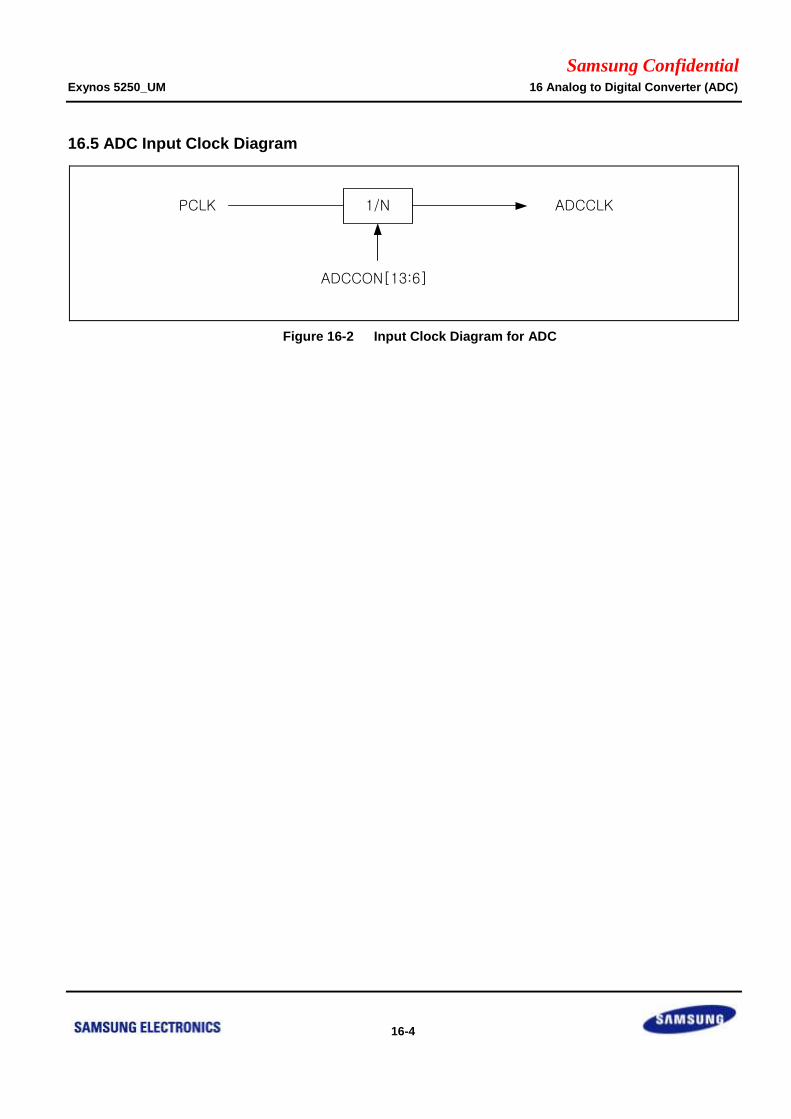
Samsung Confidential Exynos 5250_UM 16 Analog to Digital Converter (ADC)
16-4
16.5 ADC Input Clock Diagram
PCLK 1/N ADCCLK
ADCCON[13:6]
Figure 16-2 Input Clock Diagram for ADC
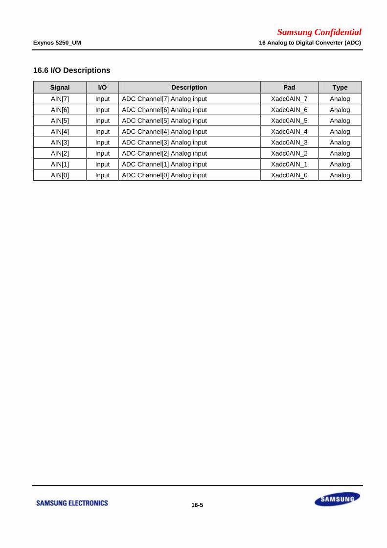
Samsung Confidential Exynos 5250_UM 16 Analog to Digital Converter (ADC)
16-5
16.6 I/O Descriptions
Signal I/O Description Pad Type
AIN[7] Input ADC Channel[7] Analog input Xadc0AIN_7 Analog
AIN[6] Input ADC Channel[6] Analog input Xadc0AIN_6 Analog
AIN[5] Input ADC Channel[5] Analog input Xadc0AIN_5 Analog
AIN[4] Input ADC Channel[4] Analog input Xadc0AIN_4 Analog
AIN[3] Input ADC Channel[3] Analog input Xadc0AIN_3 Analog
AIN[2] Input ADC Channel[2] Analog input Xadc0AIN_2 Analog
AIN[1] Input ADC Channel[1] Analog input Xadc0AIN_1 Analog
AIN[0] Input ADC Channel[0] Analog input Xadc0AIN_0 Analog
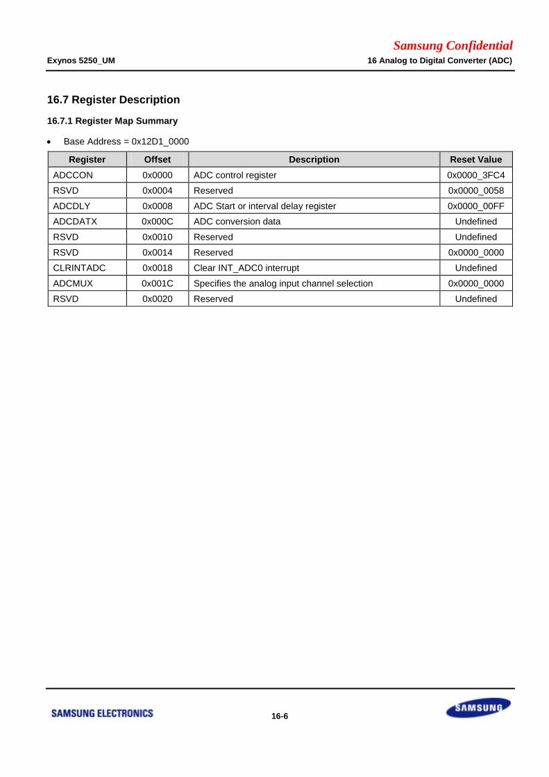
Samsung Confidential Exynos 5250_UM 16 Analog to Digital Converter (ADC)
16-6
16.7 Register Description
16.7.1 Register Map Summary
Base Address = 0x12D1_0000
Register Offset Description Reset Value
ADCCON 0x0000 ADC control register 0x0000_3FC4
RSVD 0x0004 Reserved 0x0000_0058
ADCDLY 0x0008 ADC Start or interval delay register 0x0000_00FF
ADCDATX 0x000C ADC conversion data Undefined
RSVD 0x0010 Reserved Undefined
RSVD 0x0014 Reserved 0x0000_0000
CLRINTADC 0x0018 Clear INT_ADC0 interrupt Undefined
ADCMUX 0x001C Specifies the analog input channel selection 0x0000_0000
RSVD 0x0020 Reserved Undefined
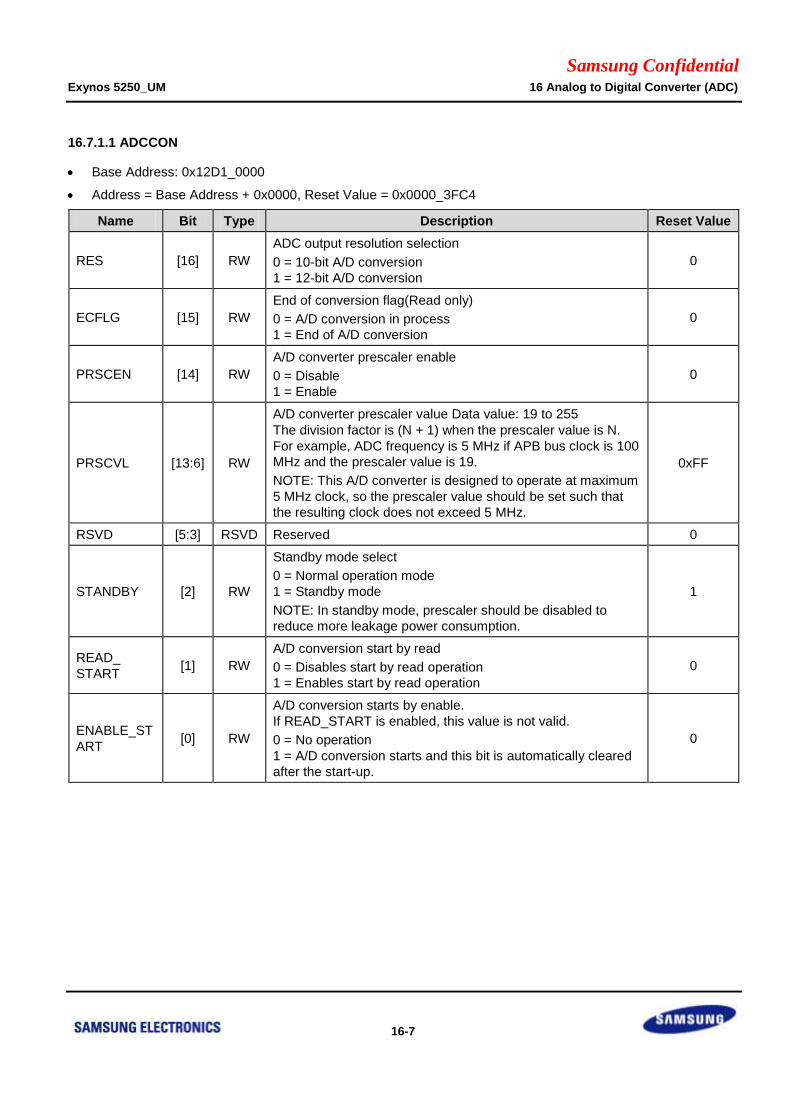
Samsung Confidential Exynos 5250_UM 16 Analog to Digital Converter (ADC)
16-7
16.7.1.1 ADCCON
Base Address: 0x12D1_0000
Address = Base Address + 0x0000, Reset Value = 0x0000_3FC4
Name Bit Type Description Reset Value
RES [16] RW
ADC output resolution selection
0 = 10-bit A/D conversion
1 = 12-bit A/D conversion
0
ECFLG [15] RW
End of conversion flag(Read only)
0 = A/D conversion in process
1 = End of A/D conversion
0
PRSCEN [14] RW
A/D converter prescaler enable
0 = Disable
1 = Enable
0
PRSCVL [13:6] RW
A/D converter prescaler value Data value: 19 to 255
The division factor is (N + 1) when the prescaler value is N.
For example, ADC frequency is 5 MHz if APB bus clock is 100
MHz and the prescaler value is 19.
NOTE: This A/D converter is designed to operate at maximum
5 MHz clock, so the prescaler value should be set such that
the resulting clock does not exceed 5 MHz.
0xFF
RSVD [5:3] RSVD Reserved 0
STANDBY [2] RW
Standby mode select
0 = Normal operation mode
1 = Standby mode
NOTE: In standby mode, prescaler should be disabled to
reduce more leakage power consumption.
1
READ_
START [1] RW
A/D conversion start by read
0 = Disables start by read operation
1 = Enables start by read operation
0
ENABLE_ST
ART [0] RW
A/D conversion starts by enable.
If READ_START is enabled, this value is not valid.
0 = No operation
1 = A/D conversion starts and this bit is automatically cleared
after the start-up.
0
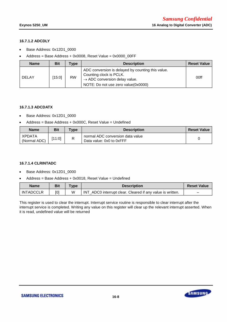
Samsung Confidential Exynos 5250_UM 16 Analog to Digital Converter (ADC)
16-8
16.7.1.2 ADCDLY
Base Address: 0x12D1_0000
Address = Base Address + 0x0008, Reset Value = 0x0000_00FF
Name Bit Type Description Reset Value
DELAY [15:0] RW
ADC conversion is delayed by counting this value.
Counting clock is PCLK.
ADC conversion delay value.
NOTE: Do not use zero value(0x0000)
00ff
16.7.1.3 ADCDATX
Base Address: 0x12D1_0000
Address = Base Address + 0x000C, Reset Value = Undefined
Name Bit Type Description Reset Value
XPDATA
(Normal ADC) [11:0] R
normal ADC conversion data value
Data value: 0x0 to 0xFFF 0
16.7.1.4 CLRINTADC
Base Address: 0x12D1_0000
Address = Base Address + 0x0018, Reset Value = Undefined
Name Bit Type Description Reset Value
INTADCCLR [0] W INT_ADC0 interrupt clear. Cleared if any value is written. –
This register is used to clear the interrupt. Interrupt service routine is responsible to clear interrupt after the
interrupt service is completed. Writing any value on this register will clear up the relevant interrupt asserted. When
it is read, undefined value will be returned
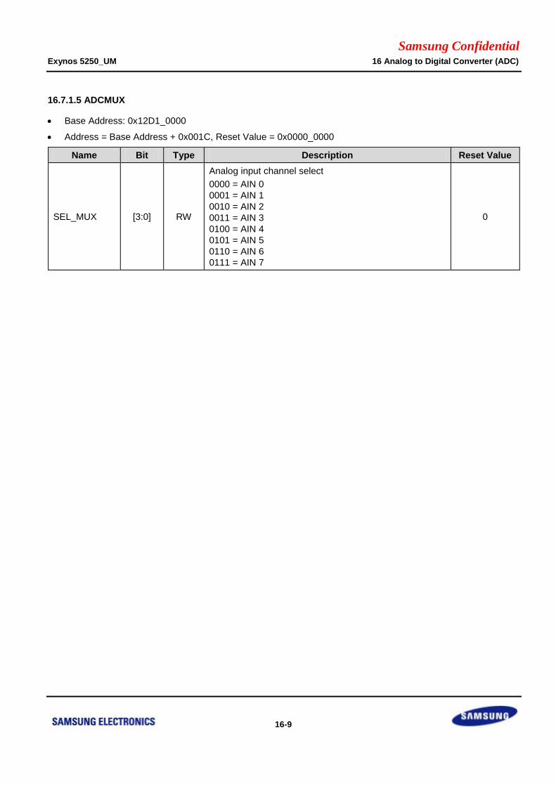
Samsung Confidential Exynos 5250_UM 16 Analog to Digital Converter (ADC)
16-9
16.7.1.5 ADCMUX
Base Address: 0x12D1_0000
Address = Base Address + 0x001C, Reset Value = 0x0000_0000
Name Bit Type Description Reset Value
SEL_MUX [3:0] RW
Analog input channel select
0000 = AIN 0
0001 = AIN 1
0010 = AIN 2
0011 = AIN 3
0100 = AIN 4
0101 = AIN 5
0110 = AIN 6
0111 = AIN 7
0


![Quantum Performance E ects - Aleksey ShipilëvUbuntu 13.10 (64-bit) Samsung Exynos 4412, ARMv7 (Cortex-A9) [1.6 GHz] 1x4x1 Linaro 12.11 1 System Under Test Slide 6/45. Intro: SUTs](https://static.fdocuments.net/doc/165x107/5f82934d249d2b459a3ba448/quantum-performance-e-ects-aleksey-shipilv-ubuntu-1310-64-bit-samsung-exynos.jpg)


