Chirp coded ultrasonic pulses used for scanning acoustic ...
| 1 | PVA TePla Analytical Systems GmbH
- C o m p a n y C o n f i d e n t i a l -
SAM failure analysis using scanning acoustic microscopy for diagnostics
of electronic devices and 3 D system integration technologies
Dr. Peter Czurratis1), Peter Hoffrogge 1), Dr. Sebastian Brand2), Frank Altmann2), Prof. Dr. Matthias Petzold2)
1) PVA Tepla Analytical Systems GmbH, Westhausen, Germany
2) Fraunhofer Institute for Mechanics of Materials IWM, Halle (Saale), Germany

| 2 | PVA TePla Analytical Systems GmbH
- C o m p a n y C o n f i d e n t i a l -
Outline
• Motivation and Background
• Potential of Scanning Acoustic Microscopy
• Limitations & Challenges of SAM
• Technical Advances in SAM
• Analog pre-processing
• Optimized amplification
• New transducer design
• SAM in GHz-band (Resolution in the 1 µm scale)
• Results
• Summary
| 3 | PVA TePla Analytical Systems GmbH
- C o m p a n y C o n f i d e n t i a l -
Motivation and Background
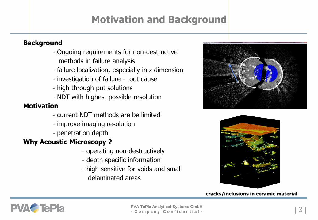
Background
- Ongoing requirements for non-destructive
methods in failure analysis
- failure localization, especially in z dimension
- investigation of failure - root cause
- high through put solutions
- NDT with highest possible resolution
Motivation
- current NDT methods are be limited
- improve imaging resolution
- penetration depth
Why Acoustic Microscopy ?
- operating non-destructively
- depth specific information
- high sensitive for voids and small
delaminated areas
cracks/inclusions in ceramic material
| 4 | PVA TePla Analytical Systems GmbH
- C o m p a n y C o n f i d e n t i a l -
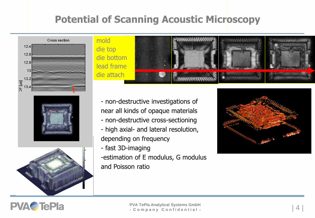
Potential of Scanning Acoustic Microscopy
- non-destructive investigations of
near all kinds of opaque materials
- non-destructive cross-sectioning
- high axial- and lateral resolution,
depending on frequency
- fast 3D-imaging
-estimation of E modulus, G modulus
and Poisson ratio
acoustic X-section of an IC
molded device
mold
die top
die bottom
lead frame
die attach

| 5 | PVA TePla Analytical Systems GmbH
- C o m p a n y C o n f i d e n t i a l -
Current limitations & Challenges
Current limitations:
- frequency vs. penetration: acoustic attenuation within the materials
- penetration depth (lens aperture, focussing, frequency)
- resolution (wavelength depending on sound velocity)
- requires coupling fluid (impedance matching)
- throughput scanning speed
x1; yn x2; yn x3; yn xn; yn
x1; y1 x2; y1 x3; y1 xn; y1
2D-scan required
Attenuation vs. Frequency
| 6 | PVA TePla Analytical Systems GmbH
- C o m p a n y C o n f i d e n t i a l -
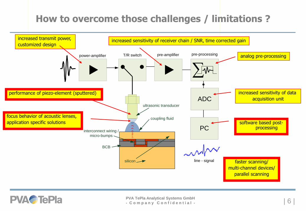
How to overcome those challenges / limitations ?
ADC
PC
ultrasonic transducer
coupling fluid
silicon
BCB
interconnect wiring /
micro-bumps
∑T/R switch pre-amplifier pre-processing
line - signal
power-amplifier
increased transmit power,
customized design increased sensitivity of receiver chain / SNR, time corrected gain
performance of piezo-element (sputtered)
focus behavior of acoustic lenses,
application specific solutions
analog pre-processing
increased sensitivity of data
acquisition unit
software based post- processing
faster scanning/
multi-channel devices/
parallel scanning
| 7 | PVA TePla Analytical Systems GmbH
- C o m p a n y C o n f i d e n t i a l -
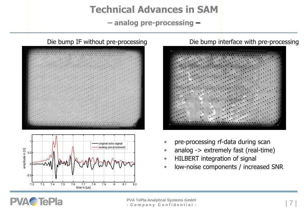
Technical Advances in SAM
– analog pre-processing –
• pre-processing rf-data during scan
• analog -> extremely fast (real-time)
• HILBERT integration of signal
• low-noise components / increased SNR
Die bump interface with pre-processing Die bump IF without pre-processing
| 8 | PVA TePla Analytical Systems GmbH
- C o m p a n y C o n f i d e n t i a l -
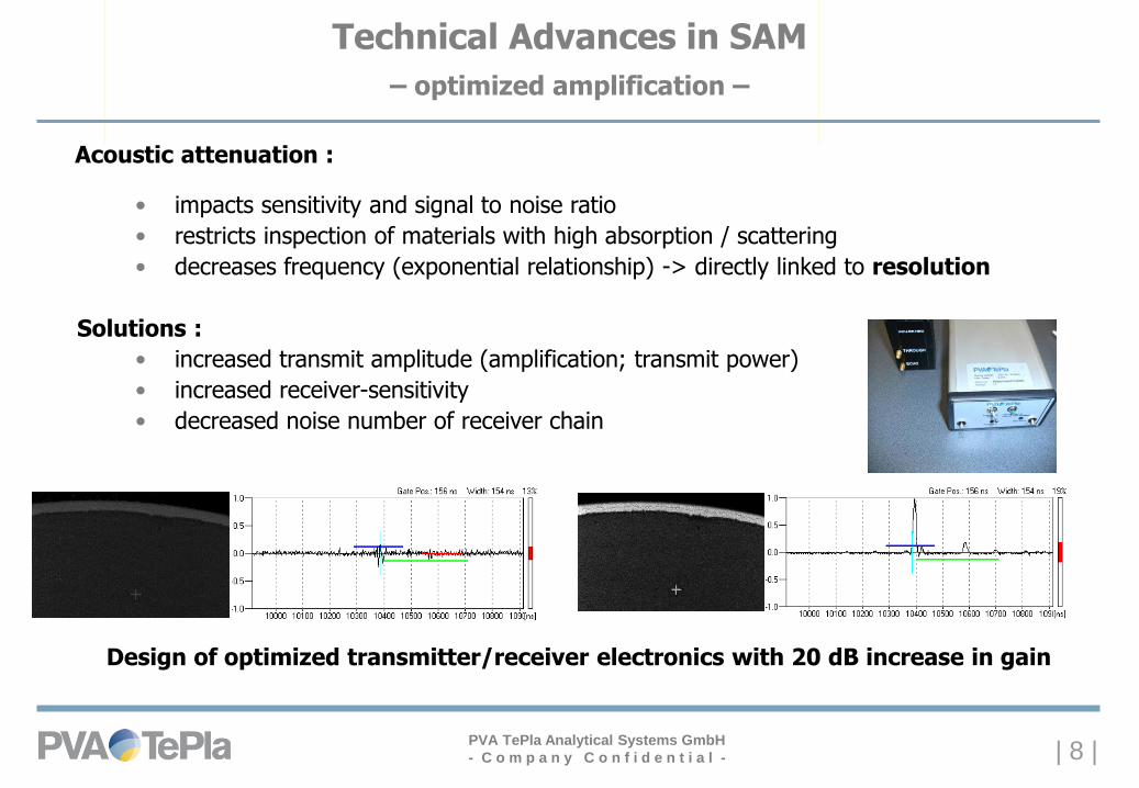
Technical Advances in SAM
– optimized amplification –
• impacts sensitivity and signal to noise ratio
• restricts inspection of materials with high absorption / scattering
• decreases frequency (exponential relationship) -> directly linked to resolution
• increased transmit amplitude (amplification; transmit power)
• increased receiver-sensitivity
• decreased noise number of receiver chain
Acoustic attenuation :
Solutions :
Design of optimized transmitter/receiver electronics with 20 dB increase in gain
| 9 | PVA TePla Analytical Systems GmbH
- C o m p a n y C o n f i d e n t i a l -
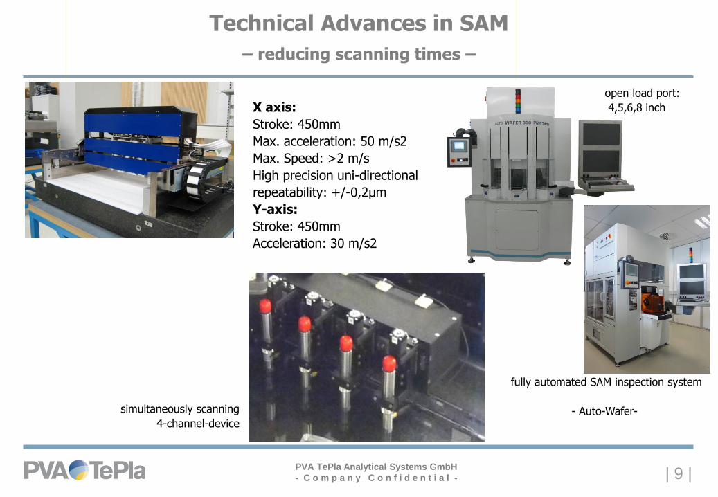
Technical Advances in SAM
– reducing scanning times –
fully automated SAM inspection system
- Auto-Wafer- simultaneously scanning
4-channel-device
X axis:
Stroke: 450mm
Max. acceleration: 50 m/s2
Max. Speed: >2 m/s
High precision uni-directional
repeatability: +/-0,2µm
Y-axis:
Stroke: 450mm
Acceleration: 30 m/s2
open load port:
4,5,6,8 inch
| 10 | PVA TePla Analytical Systems GmbH
- C o m p a n y C o n f i d e n t i a l -
Technical Advances in SAM
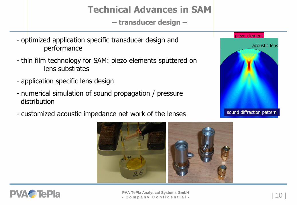
– transducer design –
- optimized application specific transducer design and performance
- thin film technology for SAM: piezo elements sputtered on lens substrates
- application specific lens design
- numerical simulation of sound propagation / pressure distribution
- customized acoustic impedance net work of the lenses
piezo element
acoustic lens
sound diffraction pattern
| 11 | PVA TePla Analytical Systems GmbH
- C o m p a n y C o n f i d e n t i a l -
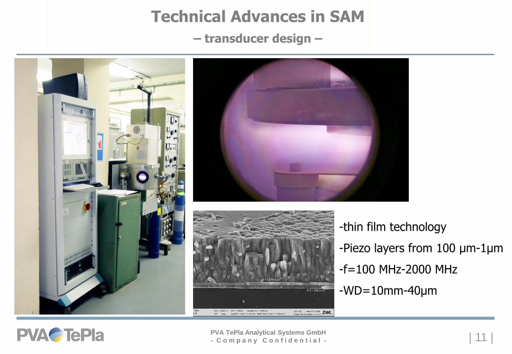
Technical Advances in SAM
– transducer design –
-thin film technology
-Piezo layers from 100 µm-1µm
-f=100 MHz-2000 MHz
-WD=10mm-40µm
| 12 | PVA TePla Analytical Systems GmbH
- C o m p a n y C o n f i d e n t i a l -
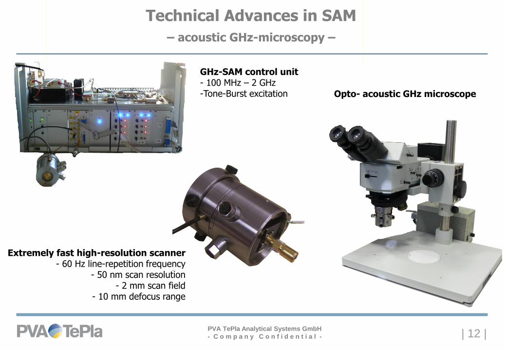
Technical Advances in SAM
– acoustic GHz-microscopy –
GHz-SAM control unit - 100 MHz – 2 GHz -Tone-Burst excitation
Extremely fast high-resolution scanner - 60 Hz line-repetition frequency
- 50 nm scan resolution - 2 mm scan field
- 10 mm defocus range
Opto- acoustic GHz microscope

| 13 | PVA TePla Analytical Systems GmbH
- C o m p a n y C o n f i d e n t i a l -
Results
| 14 | PVA TePla Analytical Systems GmbH
- C o m p a n y C o n f i d e n t i a l -
MEMS
bonded wafer
analysis

| 15 | PVA TePla Analytical Systems GmbH
- C o m p a n y C o n f i d e n t i a l -
C-scan image of bonded wafers
B-Scan
C-Scan showing the location of the B-Scan (green line)
B-Scan
delamination
Top surface
Bond interface
Key issues: through put, defect detection and
resolution, automated defect analysis

| 16 | PVA TePla Analytical Systems GmbH
- C o m p a n y C o n f i d e n t i a l -
10 µm
High resolution scans using fully automated systems: 30.000 pixel images for 12 inch wafers, 4 channels
Acqusition of >30.000 pixles/channel including DRT software: 5 µm pixel res for MEMS sensors and bonding inspection

| 17 | PVA TePla Analytical Systems GmbH
- C o m p a n y C o n f i d e n t i a l -
Quantification of bonding interfaces
Example: Si-Si molecular bonding
10.3 10.4 10.5 10.6 10.7 10.8
-0.4
-0.3
-0.2
-0.1
0
0.1
0.2
0.3
0.4
0.5
entrance echo compressional wave
bonding interface transverse wave
bonding interface
t: 10,324 µs
A: 0.27
Δt: 0ns
t: 10,518 µm
A: 0.09
Δt: 194 ns
t: 10,666 µm
A: 0.125
Δt: 342 ns
t: 10,745 µm
A: 0.47
Δt: 421 ns
Sample Amplitude 1st echo (entrance) [V]
t-echo – 1 [µs]
Amplitude 2nd interface [V]
t-echo – 2 [µs]
Quotient A1/A2
6.1 0.303 10.292 0.09 10.537 3.36
6.2 0.337 10.33 0.085 10.504 3.96
6.3 0.299 10.323 0.080 10.519 3.73
6.4 0.297 10.328 0.080 10.52 3.7125
6.5 0.288 10.333 0.087 10.509 3.3
6.6 0.291 10.332 0.087 10.519 3.34

| 18 | PVA TePla Analytical Systems GmbH
- C o m p a n y C o n f i d e n t i a l -
Surface Profilometry using
GHz-SAM
| 19 | PVA TePla Analytical Systems GmbH
- C o m p a n y C o n f i d e n t i a l -
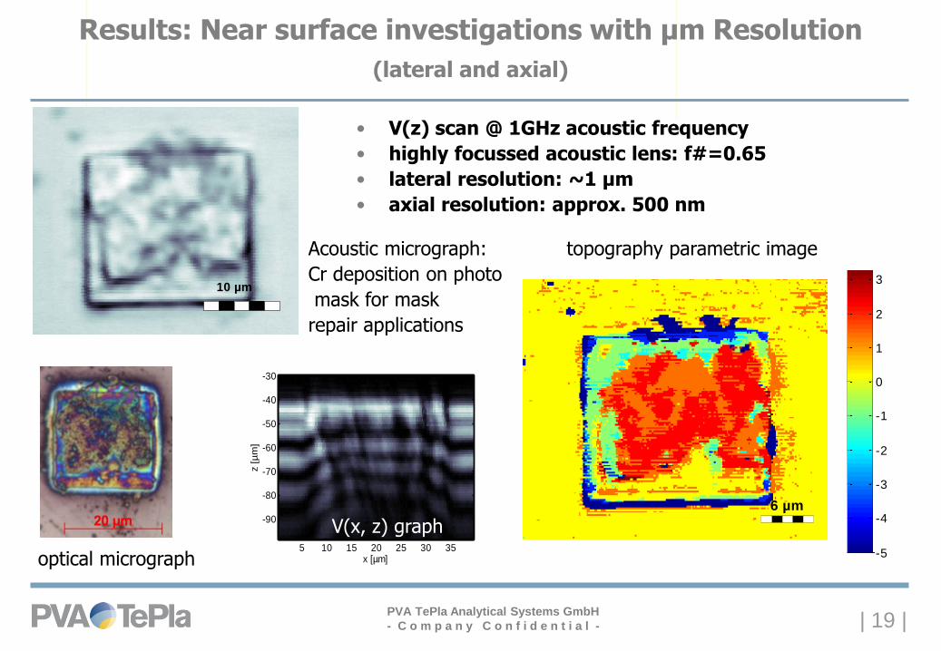
Results: Near surface investigations with µm Resolution
(lateral and axial)
10 µm
Acoustic micrograph:
Cr deposition on photo
mask for mask
repair applications
x [µm]
z [
µm
]
5 10 15 20 25 30 35
-90
-80
-70
-60
-50
-40
-30
V(x, z) graph
optical micrograph
6 µm
-5
-4
-3
-2
-1
0
1
2
3
topography parametric image
• V(z) scan @ 1GHz acoustic frequency
• highly focussed acoustic lens: f#=0.65
• lateral resolution: ~1 µm
• axial resolution: approx. 500 nm
| 20 | PVA TePla Analytical Systems GmbH
- C o m p a n y C o n f i d e n t i a l -
Inspecting
µ-Bump Devices using
GHz-SAM
| 21 | PVA TePla Analytical Systems GmbH
- C o m p a n y C o n f i d e n t i a l -
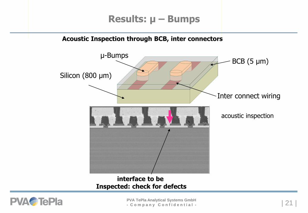
Results: µ – Bumps
Acoustic Inspection through BCB, inter connectors
BCB (5 µm)
Inter connect wiring
Silicon (800 µm)
µ-Bumps
acoustic inspection
interface to be Inspected: check for defects

| 22 | PVA TePla Analytical Systems GmbH
- C o m p a n y C o n f i d e n t i a l -
Results: µ – Bumps
@ 1 GHz acoustic frequency resolution 1 µm
30 µm
x [µm]
z [µ
m]
20 40 60 80 100 120 140-90
-80
-70
-60
-50
-40
-30
20 µm
acoustic micrograph (surface in focus)
acoustic X-section recorded at increasing defocus positions
(transducer stepwise moved toward sample)
acoustic micrograph at
-10 µm defocus; imaging of
interfaces behind BCB key
arrows correspond to position
in X-section scan
X-section along red marker

| 23 | PVA TePla Analytical Systems GmbH
- C o m p a n y C o n f i d e n t i a l -
20 µm
10 µm
µ - pillar
SAM image
SAM image
SEM image
- delaminations clearly visible
- 1 µm resolution
Results: µ – bumps delamination inspection
@ 1 GHz acoustic frequency resolution 1 µm
| 24 | PVA TePla Analytical Systems GmbH
- C o m p a n y C o n f i d e n t i a l -
Delamination Analysis in Stacked Devices
using
post-Processing in SAM

| 25 | PVA TePla Analytical Systems GmbH
- C o m p a n y C o n f i d e n t i a l -
device in flip-chip technology, BGA for electrical connections
connection defects : cracks disconnection
30 mm
20 m
m
80µm
75
0 µ
m1
00
µm
60
0 µ
m
lead frame: copper
chip: silicon
Investigations of flip chip devices
| 26 | PVA TePla Analytical Systems GmbH
- C o m p a n y C o n f i d e n t i a l -
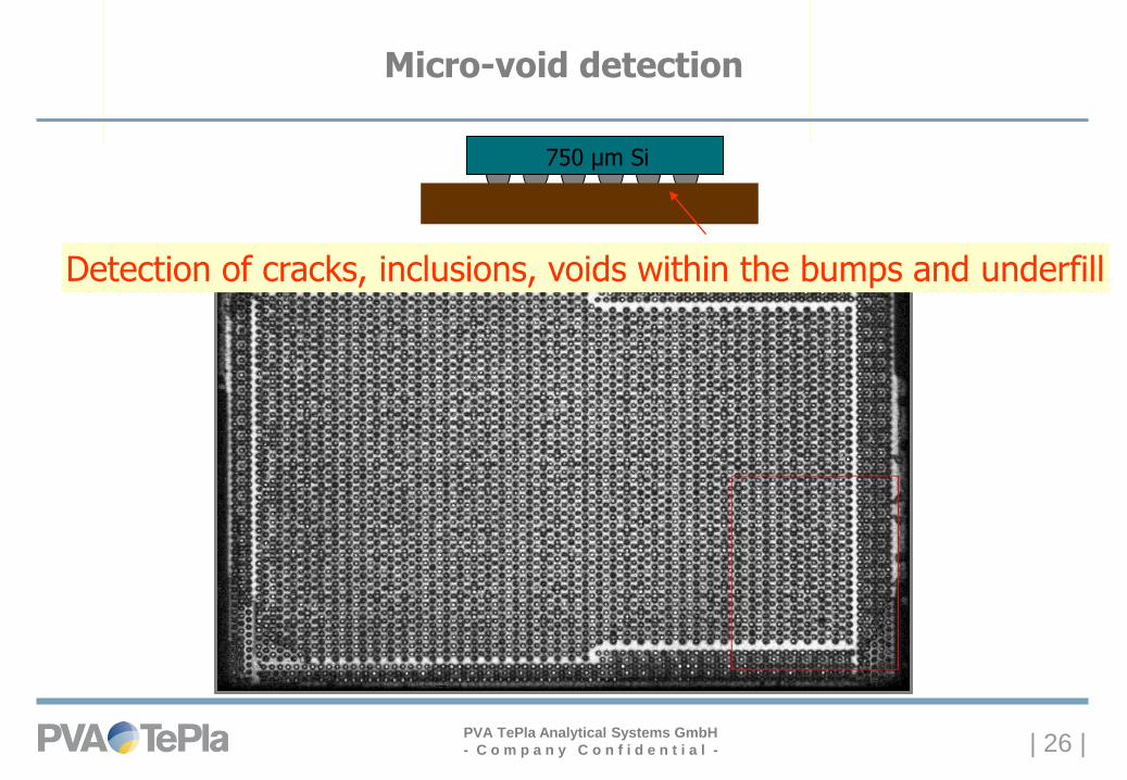
Micro-void detection
750 µm Si
Detection of cracks, inclusions, voids within the bumps and underfill
| 27 | PVA TePla Analytical Systems GmbH
- C o m p a n y C o n f i d e n t i a l -
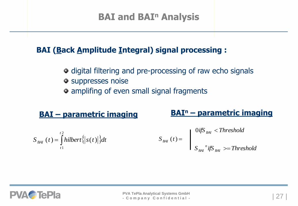
BAI and BAIn Analysis
digital filtering and pre-processing of raw echo signals
suppresses noise
amplifing of even small signal fragments
)(tS BAI
ThresholdifS BAI 0
ThresholdifSS BAI
n
BAI
2
1
)()(
t
t
BAI dttshilberttS
BAI – parametric imaging BAIn – parametric imaging
BAI (Back Amplitude Integral) signal processing :
| 28 | PVA TePla Analytical Systems GmbH
- C o m p a n y C o n f i d e n t i a l -
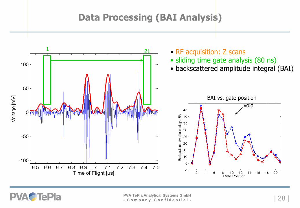
Data Processing (BAI Analysis)
• RF acquisition: Z scans • sliding time gate analysis (80 ns) • backscattered amplitude integral (BAI)
BAI vs. gate position
void
1 21
| 29 | PVA TePla Analytical Systems GmbH
- C o m p a n y C o n f i d e n t i a l -
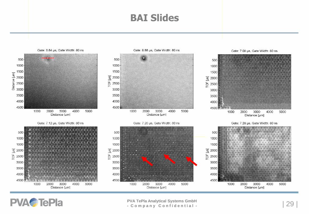
BAI Slides
| 30 | PVA TePla Analytical Systems GmbH
- C o m p a n y C o n f i d e n t i a l -
TO
F [
us]
position [um]3000 3500 4000 4500 5000
6.8
6.9
7
7.1
7.2
7.3
7.4
x 10-6
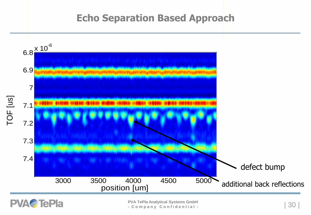
defect bump
Echo Separation Based Approach
additional back reflections

| 31 | PVA TePla Analytical Systems GmbH
- C o m p a n y C o n f i d e n t i a l -
detected from acoustic data
verified by X-ray microscopy
verified by cross sectional SEM imaging
X-ray Microscopy: missed 6 BGA defects
Acoustic Microscopy: detected missed defects
Result Verification by SEM/XRAY/SAM
| 32 | PVA TePla Analytical Systems GmbH
- C o m p a n y C o n f i d e n t i a l -
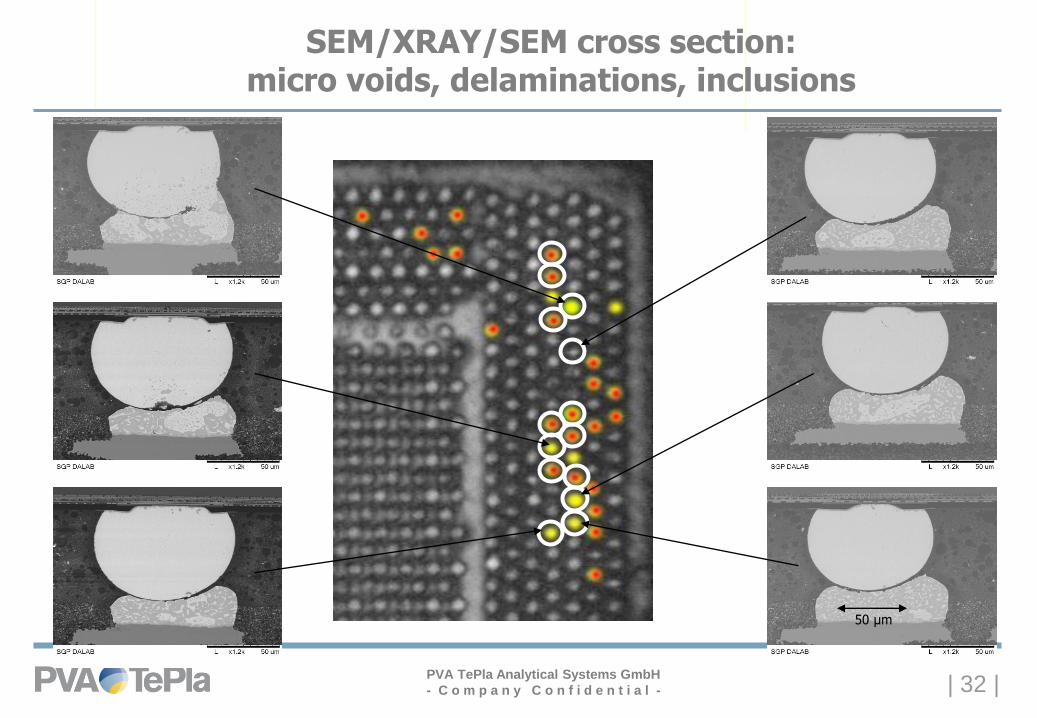
50 µm
SEM/XRAY/SEM cross section: micro voids, delaminations, inclusions
| 33 | PVA TePla Analytical Systems GmbH
- C o m p a n y C o n f i d e n t i a l -
Velocity estimation of acoustic longitudinal and transverse wave modes using scanning acoustic microscopy and derivation of elastic property-
maps

| 34 | PVA TePla Analytical Systems GmbH
- C o m p a n y C o n f i d e n t i a l -
Material properties
Z2
Z1
Z1
I0
IR1
IR2
IT1
IT2
d
dt
US-transducer derivatives :
density:
stiffness:
e-modulus:
shear modulus:
bulk modulus:
Poisson ratio:
l
l
Z
2
11 lc
2
44 sG c
44 11
44 11
1 2
2(1 )
c c
c c
11
(1 )(1 2 )
(1 )E c
11 44
4
3 B c c
preconditions:
• linear elastic
• homogeneous • isotropic • non- dispersive
| 35 | PVA TePla Analytical Systems GmbH
- C o m p a n y C o n f i d e n t i a l -
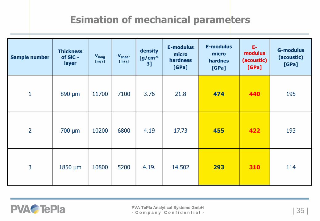
Sample number Thickness
of SiC - layer
vlong
[m/s]
vshear
[m/s]
density
[g/cm^3]
E-modulus
micro hardness
[GPa]
E-modulus
micro
hardnes
[GPa]
E-modulus
(acoustic)
[GPa]
G-modulus
(acoustic)
[GPa]
1 890 µm 11700 7100 3.76 21.8 474 440 195
2 700 µm 10200 6800 4.19 17.73 455 422 193
3 1850 µm 10800 5200 4.19. 14.502 293 310 114
Esimation of mechanical parameters
| 36 | PVA TePla Analytical Systems GmbH
- C o m p a n y C o n f i d e n t i a l -
Summary & Conclusions
• Need for NDT for ongoing improvement of SAM-equipment to increase performance
• Focus: optimization in electronics, transducers and software-tools
• Addressing signal power, penetration depth, attenuation, resolution and frequency
• Extending the fields of application for 3D-integrated devices:
• defect analysis in layered structures
• µ-bump inspection
• high resolution SAM inspection for thin layers
• fully automated control of IGBT modules, MEMS and bonded devices
• applicable in failure analysis and process control for 3D-manufacturing
• ongoing quantification of SAM measurements (E-modulus e.g.)
Technical advances
Results
Future Work