
S. Zheng and John Keane - Collider-Accelerator … · C-A/AP/97 May 2003 Modeling and Simulation of...
14
C-A/AP/97 May 2003 Modeling and Simulation of the Power Amplifier for the RHIC 28 MHz Accelerating Cavity S. Zheng and John Keane Collider-Accelerator Department Brookhaven National Laboratory Upton, NY 11973
Transcript of S. Zheng and John Keane - Collider-Accelerator … · C-A/AP/97 May 2003 Modeling and Simulation of...
C-A/AP/97 May 2003
Modeling and Simulation of the Power Amplifier for the RHIC 28 MHz Accelerating Cavity
S. Zheng and John Keane
Collider-Accelerator Department Brookhaven National Laboratory
Upton, NY 11973
MODELING AND SIMULATION OF THE POWER AMPLIFIER FOR THE RHIC 28 MHZ ACCELERATING CAVITY
Sanbao Zheng and John Keane
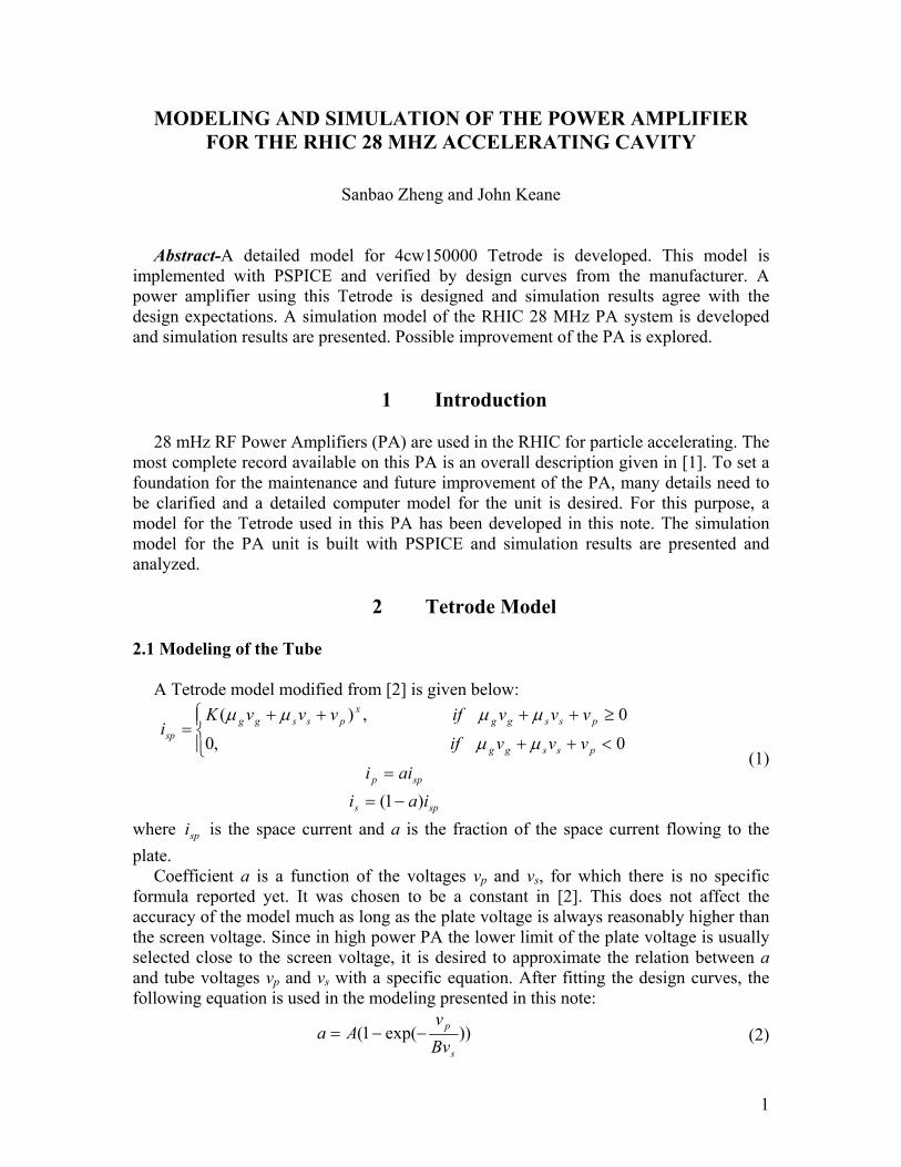
Abstract-A detailed model for 4cw150000 Tetrode is developed. This model is implemented with PSPICE and verified by design curves from the manufacturer. A power amplifier using this Tetrode is designed and simulation results agree with the design expectations. A simulation model of the RHIC 28 MHz PA system is developed and simulation results are presented. Possible improvement of the PA is explored.
1 Introduction
28 mHz RF Power Amplifiers (PA) are used in the RHIC for particle accelerating. The most complete record available on this PA is an overall description given in [1]. To set a foundation for the maintenance and future improvement of the PA, many details need to be clarified and a detailed computer model for the unit is desired. For this purpose, a model for the Tetrode used in this PA has been developed in this note. The simulation model for the PA unit is built with PSPICE and simulation results are presented and analyzed.
2 Tetrode Model
2.1 Modeling of the Tube
A Tetrode model modified from [2] is given below:
<++
≥++++=
0,0
0,)(
pssgg
pssggx
pssggsp vvvif
vvvifvvvKi
µµ
µµµµ
spp aii =
sps iai )1( −=
(1)
where is the space current and a is the fraction of the space current flowing to the plate.
spi
Coefficient a is a function of the voltages vp and vs, for which there is no specific formula reported yet. It was chosen to be a constant in [2]. This does not affect the accuracy of the model much as long as the plate voltage is always reasonably higher than the screen voltage. Since in high power PA the lower limit of the plate voltage is usually selected close to the screen voltage, it is desired to approximate the relation between a and tube voltages vp and vs with a specific equation. After fitting the design curves, the following equation is used in the modeling presented in this note:
))exp(1(s
p
Bvv
Aa −−= (2)
1
where ‘A’ and ‘B’ are constants. ‘A’ is usually close to 1 and B determines the range of the plate voltage that influences the plate current. The relation is selected such that ‘a’ approaches a constant ‘A’ when vp goes much higher than vs and ‘a’ drops down when vp get closer to vs. This agrees with the operational characteristic of a Tetrode.
Another consideration is that when the plate voltage is lower than the screen voltage, the plate current drops down drastically. When the plate voltage goes down to zero, there will be no plate current. To take into account this effect, ‘a’ is further modified to:
<−−
≥−−
=
;))exp(1(
;))exp(1(
sps
p
s
p
sps
p
vvwhenBvv
vv
A
vvwhenBvv
Aa (3)
In [2], x is assumed to be 1.5 for all tubes. This constant turned out to be not
satisfactory for the tube used in our PA. Therefore, it is taken as a parameter to be determined.
The parameters in the above model have been found for the tube 4cw150000 by fitting the model to the design curves from manufacturer. The fitting procedure is given in Appendix I, and the parameters found are:
.5.0,98.0,103,546,147,1.2 10 ==×==== − BAKx gs µµ
2.2 PSPICE Implementation
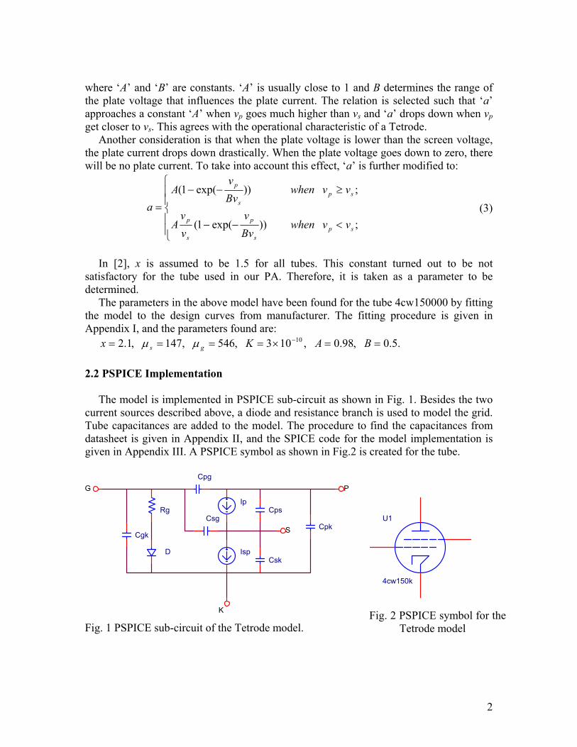
The model is implemented in PSPICE sub-circuit as shown in Fig. 1. Besides the two current sources described above, a diode and resistance branch is used to model the grid. Tube capacitances are added to the model. The procedure to find the capacitances from datasheet is given in Appendix II, and the SPICE code for the model implementation is given in Appendix III. A PSPICE symbol as shown in Fig.2 is created for the tube.
Fig. 1 PSPICE sub-circuit of the Tetrode model.
Fig. 2 PSPICE symbol for the Tetrode model
Cpg
Ip
Isp
Rg
D
Cps
Csk
CgkCpk
Csg
P
S
G
K
U1
4cw150k
2
0 2000 4000 6000 8000 10000 12000 14000 16000 18000-600
-500
-400
-300
-200
-100
0
100
200
300
400
Plate voltage (V)
Grid
vol
tage
(V)
1
5
15
30
50
80
0.1
0.5
2.0
5.0
10 15
Fig. 3. Constant-current curves (VScreen=1.5 kV) from the Tetrode model.
0 2000 4000 6000 8000 10000 12000 14000 16000 18000-700
-600
-500
-400
-300
-200
-100
0
100
200
300
400
Plate voltage (V)
Grid
vol
tage
(V)
1 5
15
30
60
0.3
1.0
2.0
4.0 8.0
Fig. 4. Constant-current curves (VScreen=2 kV) from the Tetrode model
VScreen=1.5 kV __ Plate Current --- Screen Current
VScreen=2 kV __ Plate Current --- Screen Current
3
0
0
R3200
0
V5290Vac0Vdc
T1
Z0 = 50TD = 100n
T2
Z0 = 100NL = 0.25
0 0
0
R51.37k
0
R6
0.001
U1
4cw150k
V118kv
C12
0.1u
V2
1.5kv
V3-400v
C160.1u
0 0 0
L8
100uH1 2
L9
100uH1 2
L105uH
1
2
L11100uH
1
2
C61.5n
C81.5nC9
0.1u
C10
1.5nV4290
R250
R72.5
0 0
0
L6
4uH1 2
L7
2.5uH1 2
C29n
C51.5n
0
C11
1.5n
0
0
C176.5p
0
0
R1
2
C18
14.4p0
Grid
ToGrid
ToGrid
18kv
1.5kv
-400v
18kv1.5kv-400v
in
in
Plate
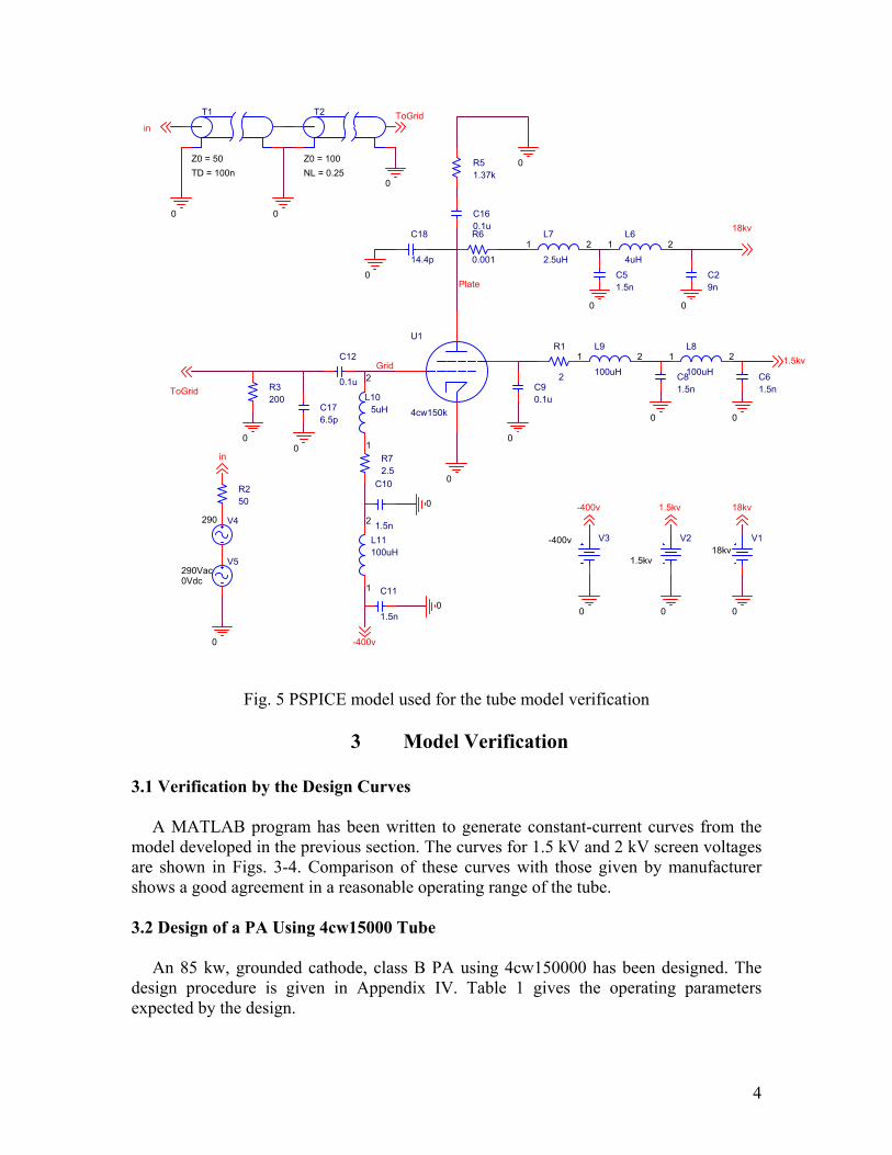
Fig. 5 PSPICE model used for the tube model verification
3 Model Verification
3.1 Verification by the Design Curves
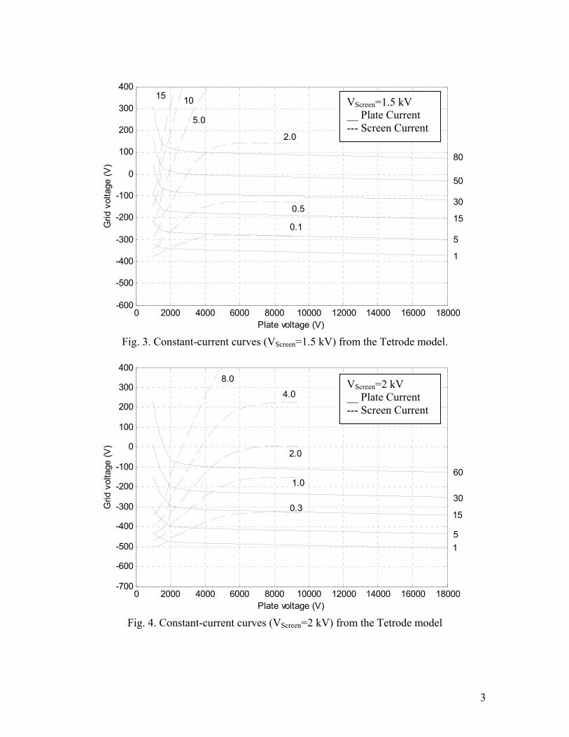
A MATLAB program has been written to generate constant-current curves from the model developed in the previous section. The curves for 1.5 kV and 2 kV screen voltages are shown in Figs. 3-4. Comparison of these curves with those given by manufacturer shows a good agreement in a reasonable operating range of the tube.
3.2 Design of a PA Using 4cw15000 Tube
An 85 kw, grounded cathode, class B PA using 4cw150000 has been designed. The design procedure is given in Appendix IV. Table 1 gives the operating parameters expected by the design.
4
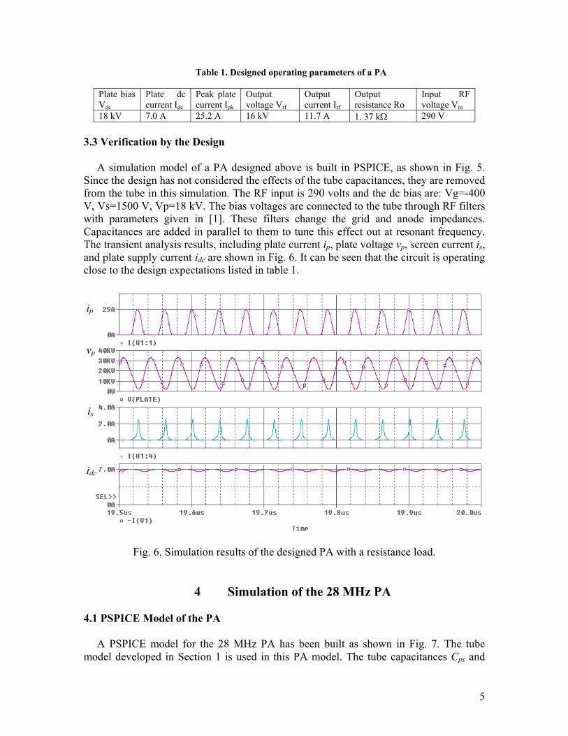
Table 1. Designed operating parameters of a PA
Plate bias Vdc
Plate dc current Idc
Peak plate current Ipk
Output voltage Vrf
Output current Irf
Output resistance Ro
Input RF voltage Vin
18 kV 7.0 A 25.2 A 16 kV 11.7 A 1. 37 kΩ 290 V 3.3 Verification by the Design
A simulation model of a PA designed above is built in PSPICE, as shown in Fig. 5. Since the design has not considered the effects of the tube capacitances, they are removed from the tube in this simulation. The RF input is 290 volts and the dc bias are: Vg=-400 V, Vs=1500 V, Vp=18 kV. The bias voltages are connected to the tube through RF filters with parameters given in [1]. These filters change the grid and anode impedances. Capacitances are added in parallel to them to tune this effect out at resonant frequency. The transient analysis results, including plate current ip, plate voltage vp, screen current is, and plate supply current idc are shown in Fig. 6. It can be seen that the circuit is operating close to the design expectations listed in table 1.
Fig. 6. Simulation results of the designed PA with a resistance load.
ip
vp
is
idc
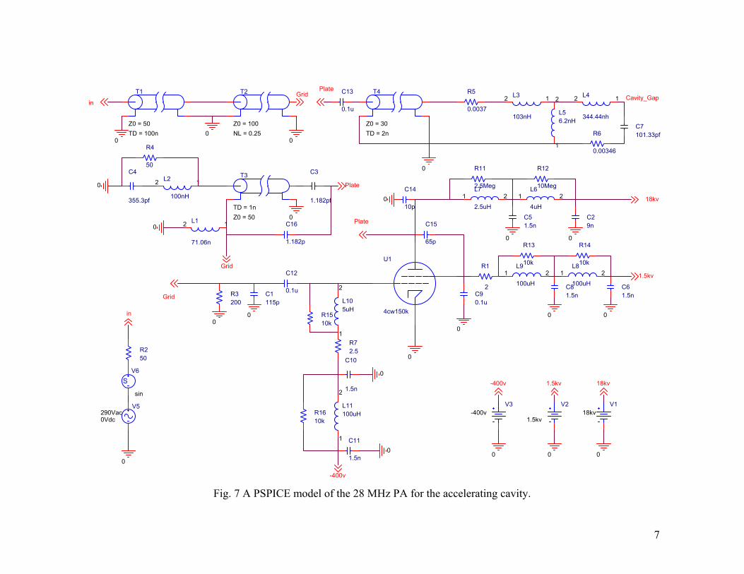
4 Simulation of the 28 MHz PA 4.1 PSPICE Model of the PA
A PSPICE model for the 28 MHz PA has been built as shown in Fig. 7. The tube model developed in Section 1 is used in this PA model. The tube capacitances Cps and
5
Cgp are taken out from the tube and connected externally for convenience of current measurements. A resistor is added in parallel to each filter inductance to model the loss in the coil.
In Fig. 7, the cavity model and the neutralization circuit model are those given in [1]. The cavity model is comprised of a piece of transmission line, a coupling loop and an equivalent series resonant circuit for the cavity itself. The neutralization model consists of a short piece of transmission line, an inductance caused by the outer conductor of the transmission line, and a notch filter that intends to provide a short circuit at 28 MHz and a 50 Ω termination at other frequencies.
The load comprised of the cavity and the tube output capacitance (65 pf) has an impedance of about 1500 Ω at resonance. It was found that the RF filter in the anode blocking circuit reduces the load impedance at resonance to around 1200 Ω. If all other operating conditions keep unchanged, a small load impedance means a lower output voltage. To compensate this effect, a capacitor in parallel to the load may be added or a redesign of the filter might be necessary. 4.2 Simulation Results
The simulation in this section uses the same RF input and dc bias as those in Section 2.
AC sweep simulation results are shown in Fig. 8. It can be seen that at the resonant frequency, the load impedance is about 1.2 kΩ. The plate current, the plate voltage and the cavity voltage are a little smaller than expected. This is because the AC sweep is a linear analysis, and only the fundamental harmonic is analyzed. The high non-linear characteristic of the tube has not been considered. The hump on the plate current curve is caused by the parasitic capacitances of the tube.
If the AC sweep range is expanded a little beyond the cavity resonant frequency, a noticeable phenomenon comes into the picture as shown in Fig. 9: a resonance much bigger in magnitude exists at around 37 MHz. It is introduced by the coupling loop and was very possibly the cause for the trouble of oscillation which occurred before.
To see the detailed waveforms of the circuit, transient analysis of the circuit operating at the cavity resonance frequency has been performed. Fig. 10 shows the simulation results after the circuit reached its steady state. It’s evident that the actual magnitude of the quantities are bigger than those obtained from ac sweep analysis. The last two curves in Fig. 10 show the current flowing through the feed-through capacitance Cpg of the tube, which can not be measured in real circuit, and the current flowing through the outer conductor of the short piece of cable used for neutralization. It is evident that these two current are equal in magnitude and in phase. This means the feedback current through Cpg is bypassed from the grid circuit by the neutralization cable and hence miller’s effect is reduced.
The Fourier analysis results for the plate current, plate voltage, and cavity voltage are shown in Fig. 11, from which all the harmonics of the operational waveform can be seen.
6
0
R5
0.0037
0
R6
0.00346
C1115p
R3200
0
C7101.33pf
L3
103nH
12 L4
344.44nh
12
0
L56.2nH
1
2T4
Z0 = 30TD = 2n
0 R11
2.5Meg
R12
10MegL6
4uH1 2
L7
2.5uH1 2
C51.5n
C90.1u
V5290Vac0Vdc
R13
10k
R14
10k
R1510k
R1610k
T1
Z0 = 50TD = 100n
T2
Z0 = 100NL = 0.25
00
0
C13
0.1u
U1
4cw150k
C14
10p0
V118kv
C12
0.1u
V2
1.5kv
V3-400v
0
C15
65p
0 0
L8
100uH1 2
L9
100uH1 2
L105uH
1
2
L11100uH
1
2
C61.5n
C81.5n
C10
1.5n
T3
TD = 1nZ0 = 50
R4
50C3
1.182pf
C4
355.3pf
L1
71.06n
12
L2
100nH
12
0
R250
0
0
R72.5
0 0
C29n
0
0
C11
1.5n
0
0
C16
1.182p
0
SV6
sin
R1
2
Plate
Cavity_GapPlate
Grid
Grid
18kv
1.5kv
-400v
18kv1.5kv-400v
in
in
Plate
Grid
Fig. 7 A PSPICE model of the 28 MHz PA for the accelerating cavity.
7
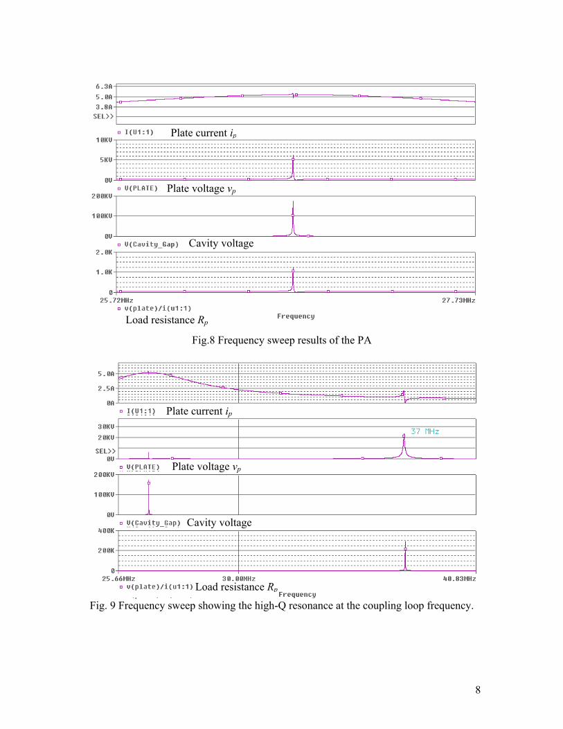
Fig. 9 Frequency
Load res
Plate current ip
Fig.8 Frequency sweep results of the PA
swee
Cavity voltage
istance Rp
Plate voltage vp
Plate current ip
Plate voltage vp
Cavity voltage
p
Load resistance Rp showing the high-Q resonance at the coupling loop frequency.
8
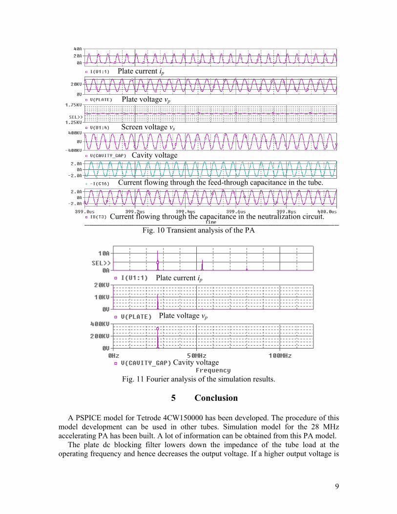
Fig. 10 Transient analysis of the PA
Fig. 11 Fourier analysis of the simulation results.
Plate current ip
Plate voltage vp
Screen voltage vs
Cavity voltage
Current flowing through the feed-through capacitance in the tube.
Current flowing through the capacitance in the neutralization circuit.
Plate current ip
Plate voltage vp
Cavity voltage
5 Conclusion
A PSPICE model for Tetrode 4CW150000 has been developed. The procedure of this
model development can be used in other tubes. Simulation model for the 28 MHz accelerating PA has been built. A lot of information can be obtained from this PA model.
The plate dc blocking filter lowers down the impedance of the tube load at the operating frequency and hence decreases the output voltage. If a higher output voltage is
9
desired, the filter may need to be redesigned or a capacitor may be used for compensation.
A resonant frequency of about 37 mHz is introduced by the coupling loop in the cavity. The tube plate sees a very big impedance (about 300 kΩ) at this frequency. A big voltage will be produced if the stimulus at this frequency exists. If this is the case, self-sustaining oscillation might happen because of the feed-through capacitance of the tube provide a positive feedback to the grid circuit. This should be further investigated in the future.
Acknowledgements
We would like to thank Joseph M. Brennan for providing the literatures on Vacuum Tube modeling and RF power amplifier design, and thank Richard Spitz, John Butler, and Alexander Zaltsman for their helps on understanding the RF accelerating system. Appendix I Finding the Model Parameters From the Tube’s
Constant-current Curves
1) Finding gµ
It can be seen from (1) that gµ is the slope of a constant plate current curve. From the design curve with vs=1.5 kV, ip=5 A, and vp=8 to 18 kV, it was found that:
5463.18
10
5,5.1==
==∂
∂=
VkV
AikVvvv
psg
pgµ
2) Finding sµ
Like the case with gµ , sµ can be found by calculating the derivative of vp with respect to vs while keeping ip and vg constant. This was done by using two design curves with vs=1.5 kV and 2.0 kV:
147500
546)420285(
5,423=
×+−=
==∂
∂=
VV
AiVvvv
pgs
pgµ
Because the resolution on the design curve is not very high, here the curve was extended beyond the page to get a measurement for pv∆ .
3) Finding x
Non-unity x is the major source for the non-linearity of the tube. It was found by taking the ratio of two points on the constant current curve:
10
x
psp
p
kVkVkVkV
AA
kVvkVvii
−×+×+−×+×+
===== )190(5465.114710
)285(5465.11471031
)(15)(5
10,5.12
1
thus: x=2.1
4) Finding A, B, and K
A is arbitrarily chosen to be 0.98. By fitting one point (vs=1.5 kV, vp=10 kV, ip=5 A) on the constant current curve to the plate current equation, K was found to be 3e-10.
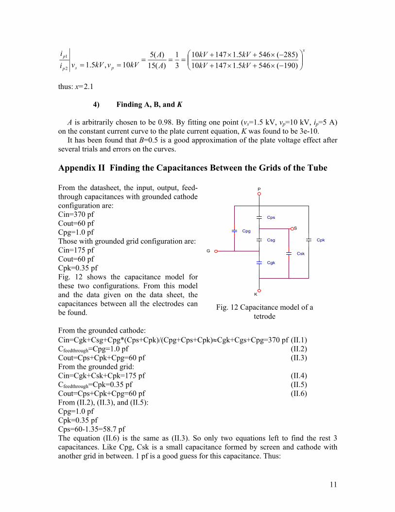
It has been found that B=0.5 is a good approximation of the plate voltage effect after several trials and errors on the curves. Appendix II Finding the Capacitances Between the Grids of the Tube From the datasheet, the input, output, feed-through capacitances with grounded cathode configuration are:
Cps
Csg
Cgk
Csk
Cpk
Cpg
P
G
S
K
Cin=370 pf Cout=60 pf Cpg=1.0 pf Those with grounded grid configuration are: Cin=175 pf Cout=60 pf Cpk=0.35 pf Fig. 12 shows the capacitance model for these two configurations. From this model and the data given on the data sheet, the capacitances between all the electrodes can be found.
Fig. 12 Capacitance model of a tetrode
From the grounded cathode: Cin=Cgk+Csg+Cpg*(Cps+Cpk)/(Cpg+Cps+Cpk)≈Cgk+Cgs+Cpg=370 pf (II.1) Cfeedthrough=Cpg=1.0 pf (II.2) Cout=Cps+Cpk+Cpg=60 pf (II.3) From the grounded grid: Cin=Cgk+Csk+Cpk=175 pf (II.4) Cfeedthrough=Cpk=0.35 pf (II.5) Cout=Cps+Cpk+Cpg=60 pf (II.6) From (II.2), (II.3), and (II.5): Cpg=1.0 pf Cpk=0.35 pf Cps=60-1.35=58.7 pf The equation (II.6) is the same as (II.3). So only two equations left to find the rest 3 capacitances. Like Cpg, Csk is a small capacitance formed by screen and cathode with another grid in between. 1 pf is a good guess for this capacitance. Thus:
11
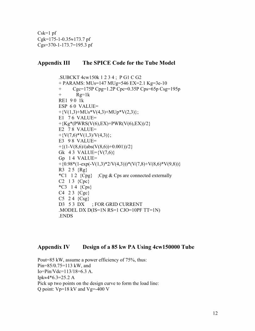
Csk=1 pf Cgk=175-1-0.35≈173.7 pf Cgs=370-1-173.7=195.3 pf Appendix III The SPICE Code for the Tube Model
.SUBCKT 4cw150k 1 2 3 4 ; P G1 C G2 + PARAMS: MUs=147 MUg=546 EX=2.1 Kg=3e-10 + Cgc=175P Cpg=1.2P Cpc=0.35P Cps=65p Csg=195p + Rg=1k RE1 9 0 1k ESP 6 0 VALUE= +V(1,3)+MUs*V(4,3)+MUp*V(2,3); E1 7 6 VALUE= +Kg*(PWRS(V(6),EX)+PWR(V(6),EX))/2 E2 7 8 VALUE= +V(7,6)*V(1,3)/V(4,3); E3 9 8 VALUE= +(1-V(8,6)/(abs(V(8,6))+0.001))/2 Gk 4 3 VALUE=V(7,6) Gp 1 4 VALUE= +0.98*(1-exp(-V(1,3)*2/V(4,3)))*(V(7,8)+V(8,6)*V(9,8)) R3 2 5 Rg *C1 1 2 Cpg ;Cpg & Cps are connected externally C2 1 3 Cpc *C3 1 4 Cps C4 2 3 Cgc C5 2 4 Csg D3 5 3 DX ; FOR GRID CURRENT .MODEL DX D(IS=1N RS=1 CJO=10PF TT=1N) .ENDS
Appendix IV Design of a 85 kw PA Using 4cw150000 Tube Pout=85 kW, assume a power efficiency of 75%, thus: Pin=85/0.75=113 kW, and Io=Pin/Vdc=113/18=6.3 A. Ipk≈4*6.3=25.2 A Pick up two points on the design curve to form the load line: Q point: Vp=18 kV and Vg=-400 V
12
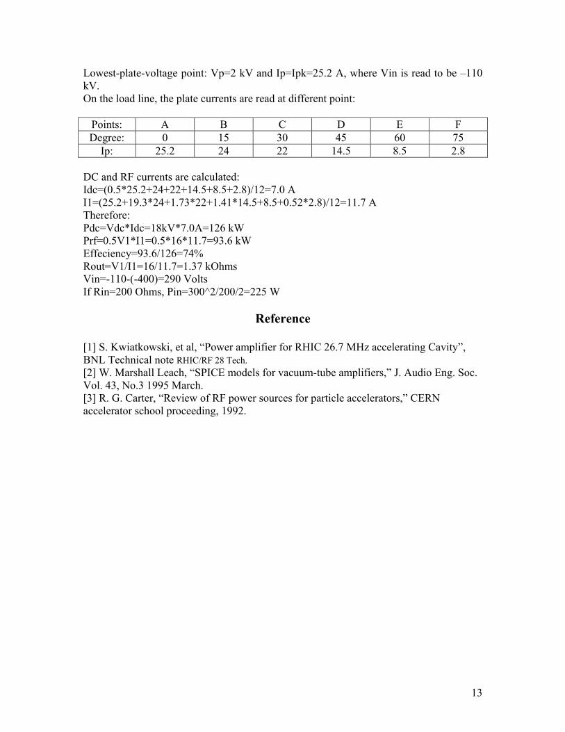
Lowest-plate-voltage point: Vp=2 kV and Ip=Ipk=25.2 A, where Vin is read to be –110 kV. On the load line, the plate currents are read at different point:
Points: A B C D E F Degree: 0 15 30 45 60 75
Ip: 25.2 24 22 14.5 8.5 2.8 DC and RF currents are calculated: Idc=(0.5*25.2+24+22+14.5+8.5+2.8)/12=7.0 A I1=(25.2+19.3*24+1.73*22+1.41*14.5+8.5+0.52*2.8)/12=11.7 A Therefore: Pdc=Vdc*Idc=18kV*7.0A=126 kW Prf=0.5V1*I1=0.5*16*11.7=93.6 kW Effeciency=93.6/126=74% Rout=V1/I1=16/11.7=1.37 kOhms Vin=-110-(-400)=290 Volts If Rin=200 Ohms, Pin=300^2/200/2=225 W
Reference
[1] S. Kwiatkowski, et al, “Power amplifier for RHIC 26.7 MHz accelerating Cavity”, BNL Technical note RHIC/RF 28 Tech. [2] W. Marshall Leach, “SPICE models for vacuum-tube amplifiers,” J. Audio Eng. Soc. Vol. 43, No.3 1995 March. [3] R. G. Carter, “Review of RF power sources for particle accelerators,” CERN accelerator school proceeding, 1992.
13