ro{r - Atlas
3
Extended Abstracts of the l99l International Conference on Solid State Devices and Materials, Yokohama, 1991, pp. 17-19 The Influence of Synchrotron X-Ray Damage on Hot-Carrier-Induced Degradation in Subquarter-Micron NMOSFETs T. Tsuchi.ya, M. Harada, K. Deguchi , and T - Matsuda NTT LSI Laboratories 3-l- Morinosato lYakamlya, Atsugi, Kanagawa 243-OL, JAPAN Hot-carri-er reliablllty due to residual damag:e in the gate oxide created by synchrotron X-ray lrradiatlon is investlgated for subquarter-mLcrometer NMOSFETS. Although lrradiation-1n- duced interface-traps are completely eliminated after 400 oC post-metallzation- annealing, neutral electron traps partlally remain. The effect of the residual traps on hot-carrler degra- dation can be negllgible when gate oxides thinner than about 5 nm are used. It ls found that there ls no effect of lrradiation damage on lnterface-trap g:eneratlon during hot-carrler-lnjec- tlon. 1. INTRODUSTIOIT Synchrotron radiation (SR) X-ray lithog- raphy ls pronlslng for fabricating future deep-subnicroneter ULSIs. However, there is a great concern over hot-carrier (HC) rell- ability due to residual damage in the gate oxide created by X-ray irradiatlon. Several projects have investigated the influence of the danage on H0-induced MOSFET degradation tll-t31. These proJects have dealt wlth greater than half-nlcroneter devices with gate oxides thicke; than-10 rn, and with relatively snall (LO" mJ/cmz) naxinun irradi- atlon doses. This paper focuses on the lrradiation and HC-effects for subquarter-nicroneter NMOSFETs with thlnner. gate oxides und'er., a wlder irradiation range (10-3,000 mJ/cn"l . 2. EXPERITIENTAL PROCEDTIRES N+ poly-Si-gate NMOSFETs with 3.5-L2.0 nn thlck gate oxldes and 80 nn deep source/d.rain Junctions [4] were used in this study. Gate layers rvere patterned by EB lithography. After gate electrode fabrica- tlon, sanples were annealed at 900 "C for 30 ninutes ln Nc atnosphere to elininate"EB danage. ExceFt f or the gate layer, opt.ical Ilthography was used. Irradiation experl- nents were performed in an NTT SOR Facility t5l. In order to lnvestigate irradlation- lnduced danage and the effect of pos!-metali- zation-anneallng, which is the final anneal- lng through fabrlcation process, direct exposure was nade without any reslst layer either before or after the final anneallng ln Nt/Hc f ornlng gas at 400 oC f or 30 ninutes. x:rai wavelengths ranged f ron o ,7 -L.2 nn!,. The naxinun irradiatlon dose (3,000 mJ/emzl A-1-4 was set to evaluate irradlatlon effects due to flve- or six-lithography-leveI exposure uslng typical-sensitivity X-ray reslst, assuning a three-level metal process where high-tenperature annealing is not perforned except for the flnal N2/H2 annealing. 3. RESTILTS AIID DISCUSSION 3.1. IRMDIATION DAIIAGE X-ray exposure generates inter- face-traps, posltlve charges and neutral traps in the gate oxlde tOl. Generated interface-traps were evalu- ated by charge punp l ng current I,^r, [7], and they are conpletely eliminafl ed after the flnal annealing, even under a maxlnun dose of 3,000 mJ/cm2, as shown ln Fig. 1. Generated posi- tive charges also disappeared after the anneallng. This was conflrned by a conparlson with M0SFET characteris- lo-7 Tor - 5.0 nm L = lOpm W = 20pm AFTER EXPOSURE lo lo2 lo3 EXPOSURE DOSE (mJ/cmzl Flg. 1 Charge pumplng current vs. exposure dose. s ro-s CL <, lo-e t7
Transcript of ro{r - Atlas

Extended Abstracts of the l99l International Conference on Solid State Devices and Materials, Yokohama, 1991, pp. 17-19
The Influence of Synchrotron X-Ray Damage on Hot-Carrier-InducedDegradation in Subquarter-Micron NMOSFETs
T. Tsuchi.ya, M. Harada, K. Deguchi , and T - Matsuda
NTT LSI Laboratories3-l- Morinosato lYakamlya, Atsugi, Kanagawa 243-OL, JAPAN
Hot-carri-er reliablllty due to residual damag:e in the gateoxide created by synchrotron X-ray lrradiatlon is investlgatedfor subquarter-mLcrometer NMOSFETS. Although lrradiation-1n-duced interface-traps are completely eliminated after 400 oC
post-metallzation- annealing, neutral electron traps partlallyremain. The effect of the residual traps on hot-carrler degra-dation can be negllgible when gate oxides thinner than about 5nm are used. It ls found that there ls no effect of lrradiationdamage on lnterface-trap g:eneratlon during hot-carrler-lnjec-tlon.
1. INTRODUSTIOITSynchrotron radiation (SR) X-ray lithog-
raphy ls pronlslng for fabricating futuredeep-subnicroneter ULSIs. However, there isa great concern over hot-carrier (HC) rell-ability due to residual damage in the gateoxide created by X-ray irradiatlon. Severalprojects have investigated the influence ofthe danage on H0-induced MOSFET degradationtll-t31. These proJects have dealt wlthgreater than half-nlcroneter devices withgate oxides thicke; than-10 rn, and withrelatively snall (LO" mJ/cmz) naxinun irradi-atlon doses. This paper focuses onthe lrradiation and HC-effects forsubquarter-nicroneter NMOSFETs withthlnner. gate oxides und'er., a wlderirradiation range (10-3,000 mJ/cn"l .
2. EXPERITIENTAL PROCEDTIRES
N+ poly-Si-gate NMOSFETs with 3.5-L2.0nn thlck gate oxldes and 80 nn deepsource/d.rain Junctions [4] were used in thisstudy. Gate layers rvere patterned by EBlithography. After gate electrode fabrica-tlon, sanples were annealed at 900 "C for 30ninutes ln Nc atnosphere to elininate"EBdanage. ExceFt f or the gate layer, opt.icalIlthography was used. Irradiation experl-nents were performed in an NTT SOR Facilityt5l. In order to lnvestigate irradlation-lnduced danage and the effect of pos!-metali-zation-anneallng, which is the final anneal-lng through fabrlcation process, directexposure was nade without any reslst layereither before or after the final anneallng lnNt/Hc f ornlng gas at 400 oC f or 30 ninutes.x:rai wavelengths ranged f ron o ,7 -L.2 nn!,.
The naxinun irradiatlon dose (3,000 mJ/emzl
A-1-4
was set to evaluate irradlatlon effects dueto flve- or six-lithography-leveI exposureuslng typical-sensitivity X-ray reslst,assuning a three-level metal process wherehigh-tenperature annealing is not perfornedexcept for the flnal N2/H2 annealing.
3. RESTILTS AIID DISCUSSION3.1. IRMDIATION DAIIAGE
X-ray exposure generates inter-face-traps, posltlve charges andneutral traps in the gate oxlde tOl.Generated interface-traps were evalu-ated by charge punp l ng current I,^r,[7], and they are conpletely eliminafled after the flnal annealing, evenunder a maxlnun dose of 3,000 mJ/cm2,as shown ln Fig. 1. Generated posi-tive charges also disappeared afterthe anneallng. This was conflrned bya conparlson with M0SFET characteris-
lo-7 Tor - 5.0 nm
L = lOpmW = 20pm
AFTEREXPOSURE
lo lo2 lo3
EXPOSURE DOSE (mJ/cmzl
Flg. 1Charge pumplng current vs. exposure dose.
s ro-sCL<,
lo-e
t7

D0SE (mJ/cm2l
3000r00o ;f133'tr
0 tor = 5.0 nm
AFTER EXPOSURE8 ANNEAL
z
= t0-'
reo
ro-'
= ro-2F
ro-l loo lolQrn.r (c/cmzl
Fts. zAV; vs. charges of electrons lnJectedf ro^m substrate QlNl.
tlcs of non-lrradiated devlces.Residual neutral traps were evaluatedby threshold voltage shift A Vr aftersubstrate hot - electron lnJection t8l.AVr due to the trapping of electronsard shown in Fis. 2 as a function oflnjected electron charg:es. AVrlncreases wi th the increase in theexposure dose, and it cannot recoverto the non-irradiated level, evenafter the final anneallng. Thls meansthat neutral traps are not completelyrecovered even after the final anneal-ing. Effects of the gate oxide thick-ness on AVr are shown ln Flg. 3 fornon-iqradiaf,ed devlces, and for 3,00OmJ/cmz-irradlated and subsequently-annealed devlces. InJected electron-charg:es are flxed at 0.5 e/cmz. AVtdramatlcally decreases as the gateoxlde thickness TOX decreases below Inm . Tox wi Il be - a key parameter lnreducin-d- the lnfluence of the residualneutral. traps on HC-degradatlon.
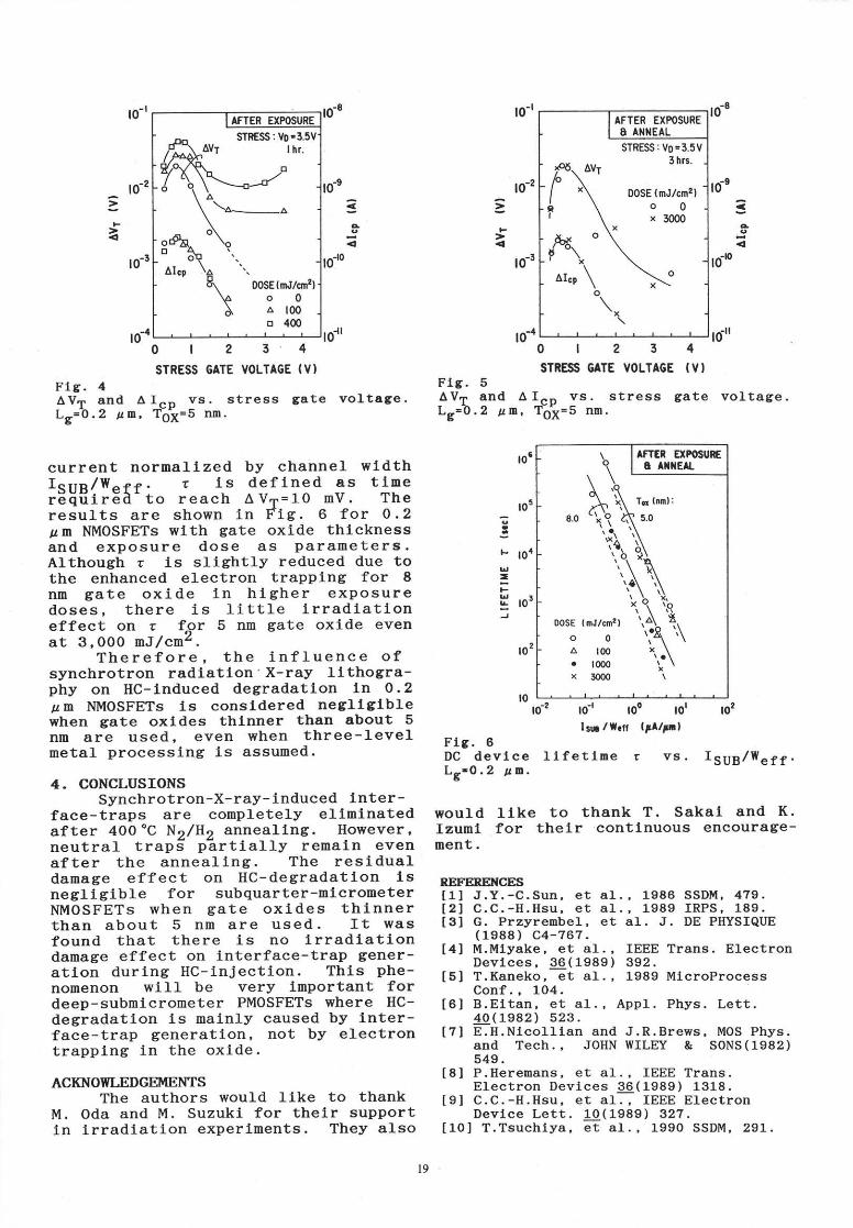
3.2. HOT CARRIER DEGRADATION3.2.L. EFFECTS OF X-RAY DAMAGE
In order to lnvestlg;ate theeffect of X-ray damage on HC-induceddevlce degradatlon 1n subquarter-mlcrometer NMOSFETS, threshold voltageshift A Vt and the increase in I"odependences upon stress gate voltps^eunder fixed stress-draln-voltage weremeasured. The bias-stress was appliedto the devices after exposure. Theresults for O.2 pm NMOSFETs are shownln Flg . 4. Compared wlth non-irradi-ated devices , A Vn increases pemarka-bly wlth incredsed exposure dose,especlally in the hlgher stress-gate-voltag;e range It should be notedthat A I^-, is not dependent on theexposure "dose, whlch means that lrra-diatlon-lnduced damage does not playany role ln lnterface-trap generatlon
lo-3
to-'o2468t012
GATE 0Xl0E THICKilESS (nml
Fle. 3Effect of gate oxlde thlckness on A Vrdue to substrate hot-electron injectionlL"=1O pm.
durlng HC-lnJection. The increase lnAVn ls clearly due to the trapping oftnJ-ecfed-hot-electrons ln the irradla-tlon-lnduced traps.
Here, lt has been reported thatHC-degradatLon 1s signlflcantly 1n-creased ln PMOSFETs due to the en-hanced electron trapping in the oxldeby the resldual traps tgl. Recently,lt was found that HC-degradation modefor quarter-mlcrometer level PMOSFETSls qul te dlfferent from prevlousreports ( 1. e. , effective channel-length reductlon due to trapped elec-trons ) , and the new degradation models caused by lnterface-traps generatedby hot-hole-lnj ectlon t 10 I . Inter-f ace-trap g:eneratlon ls a more lmpor-tant phenomenon than electron trappingfor future PMOSFETS. Therefore, thefact that there 1s no irradiation-lnduced damage effect on lnterface-trap g:eneratlon durlng HC- in j ection lshlshly slgnlflcant.3.2.2 EFFECTS OF ANNEALING AI{D GATE
OXIDE TUICNiTESS ON DEVICE LIFETIMEA V1. and A I.o dependences upo4
stress gate voltag^e for 3,000 mJ/cmo-lrradlated and subsequently-annealed0.2 pn-NMOSFETS are shown in Fig. 5.For comparison, those for non-irradi-ated devlces are also shown in theflgure. Gate oxlde thickness for bothtypes of devices is 5 nm. It can beseen that there are no meaningfuldlf f erences ln A V.n and A I,-r, betweenthe two types of ddvices. The influ-ence of X-ray damage on HC-desradatlonseems to dlsappear after the flnalanneallng. In order to investigatethe effect of the final annealing indetalI, DC device Ilfetimes r wereobtalned as a functlon of substrate
X'IDosE lmJ/cm2l /i
3ooo //\//o \//
\ / / Qlx,l= 0.5 c/cmz
x////t
i I AFrER ExPosuRE
I 'ANNEAL?
l0-l
lo-2
l0-3
td4
AFTER
00SE(mJ/cm2lo0a 100B 400 ro{r lo-{
AFTER EXPOSURE
8 ANiIEAL
STRESS: Vo=3.5V3 hrs.
DOSE (mJ/cm2lo0x 3000
to-8
ldlo
lo-e
lo-l
lo-2
to'
l0s
to8
tde
lo-10
ldrl
voltage.
e(,Att
lo-3
012STRESS GATE VOLTAGE (VI
F1s. 4AVq. and AI^^ vs. stress gate voltage.t"='o-z FEl, T-o-x=s rrm.
current normal Lzed by channel wldthISUn/Weff. t ls deflned &s tlmerEdilirdil-to reach AVr=10 mV. Theresults are shown in FiS. 6 for 0.2pm NMOSFETs with gate oxide thicknessand exposure dose as parameters.Although c is slightly reduced due tothe enhanced electron trapping for 8nm gate oxide ln hlgher exposuredoses, there is littIe irradiatlonef f ect on t f-or 5 nm gate oxlde evenat 3, O0O mJ /cm2 .
Therefore, the influence ofsynchrotron radlatlon' X-ray llthogra-phy on HC-lnduced degradatlon ln O.2pm NMOSFETs 1s consldered negllglblewhen gate oxldes thlnner than about 5nm are used, even when three-levelmetal processing ls assumed.
4. CONCLUSIONSSynchrotron-X- ray- induced lnter -
face-traps are completely ellminatedafter 4OO"C No/Hc anneallng. However,neutral traps" p-artlally remaln evenaf ter the anneallng. The resi-dualdamage effect on HC-degradatlon 1snegllgible for subquarter-mlcrometerNMOSFETs when gate oxldes thlnnerthan about 5 nm are used. It wasfound that there 1s no lrradlationdamage effect on interface-trap gener-atlon durlng HC-iniecti-on. This phe-nomenon will be very lmportant fordeep-submicrometer PMOSFETS where HC-deg:radation is mainly caused by lnter-face-trap g:eneration, not by electrontrapplng in the oxide.
ACIO.IOWLEDGEMET.ITSThe authors would llke to thank
M. Oda and M. Suzuki for thelr supportin lrradlatlon experlments. They also
STRE$i GITE VOLTAGE (VIFls. 5AVr and A Ir.r, vs. stress gatel"=b . e Ffr, T;-X=s nm .
x\
X1\ox
r\\\'\OOSE (mJ/cm2l t.
o0a t00. 1000x 3000
tdz rdr roo ror roa
ls6 /tcfi lpllpalFls.6DC devlce ltfetl-ne tLf-O .2 lr m.
vs . ISUg /V ett .
would llke to thank T. Sakal and K.Izuml for thelr contlnuous encourag:e-ment.
REFERENCESI1l J.Y.-C.Sun, €t &1., 1986 SSDM, 479.I2l C.C.-H.Hsu, €t erl., l-989 IRPS, 189.131 c. Przyrembel, et aI. J. DE PHYSIQUE
(1e88) C4-767.t41 M.Mlyake, et 8I., IEEE Trans. Electron
Devlces, 36(1989) 392.l5I T.Kaneko, et aI., L989 MlcroProcess
Conf., 104.t6l B.Eltan, €t 81., AppI. Phys. Lett.
40(1982) 523.t?l E.H.Nlcolllan and J.R.Brews, MOS Phys.
and Tech. , JOHN WILEY & SONS ( 1982)549.
t8l P.Heremans, et 8I., IEEE Trans.Electron Devices 36 ( l-989 ) 1318.
tgl C.C.-H.Hsu, €t dl., IEEE ElectronDevlce Lett. 19.(1989) 327.
t10I T.Tsuchlya, et aI., L990 SSDM, 29L.
lo{
to3
rot
e,o-F
lr,-Flrll!
J
t9


![[R. T. Curtis, R. a. Wilson] the Atlas of Groups Finite](https://static.fdocuments.net/doc/165x107/55cf96be550346d0338d83d7/r-t-curtis-r-a-wilson-the-atlas-of-groups-finite.jpg)