RIT's Advanced CMOS Process Integration
142
© April 1, 2014 Dr. Lynn Fuller RIT’s Advanced CMOS Process Integration Page 1 Rochester Institute of Technology Microelectronic Engineering ROCHESTER INSTITUTE OF TECHNOLOGY MICROELECTRONIC ENGINEERING RIT’s Advanced CMOS Process l=0.25 μm, L poly = 0.5 μm, L eff = 100nm Dr. Lynn Fuller Samarth Parikh, Chandan Amareshbabu webpage: http://people.rit.edu/lffeee/ Microelectronic Engineering Rochester Institute of Technology 82 Lomb Memorial Drive Rochester, NY 14623-5604 Tel (585) 475-2035 Fax (585) 475-5041 email: [email protected] microE webpage: http://www.microe.rit.edu 4-1-2014 AdvCmosProcessIntegration.ppt
Transcript of RIT's Advanced CMOS Process Integration

© April 1, 2014 Dr. Lynn Fuller
RIT’s Advanced CMOS Process Integration
Page 1
Rochester Institute of Technology
Microelectronic Engineering
ROCHESTER INSTITUTE OF TECHNOLOGY MICROELECTRONIC ENGINEERING
RIT’s Advanced CMOS Process l=0.25 µm, Lpoly= 0.5 µm, Leff = 100nm
Dr. Lynn Fuller Samarth Parikh, Chandan Amareshbabu
webpage: http://people.rit.edu/lffeee/
Microelectronic Engineering Rochester Institute of Technology
82 Lomb Memorial Drive Rochester, NY 14623-5604
Tel (585) 475-2035 Fax (585) 475-5041
email: [email protected] microE webpage: http://www.microe.rit.edu
4-1-2014 AdvCmosProcessIntegration.ppt

© April 1, 2014 Dr. Lynn Fuller
RIT’s Advanced CMOS Process Integration
Page 2
Rochester Institute of Technology
Microelectronic Engineering
OUTLINE
Introduction
Advanced CMOS Process Details

© April 1, 2014 Dr. Lynn Fuller
RIT’s Advanced CMOS Process Integration
Page 3
Rochester Institute of Technology
Microelectronic Engineering
INTRODUCTION
RIT is supporting two different CMOS process technologies. The older p-well CMOS and SMFL-CMOS have been phased out. The SUB-CMOS process is used for standard 3 Volt Digital and Analog integrated circuits. This is the technology of choice for teaching circuit design and fabricating CMOS circuits at RIT. The ADV-CMOS process is intended to introduce our students to process technology that is close to industry state-of-the-art. This process is used to build test structures and develop new technologies at RIT. RIT p-well CMOS l = 4 µm Lmin = 8 µm RIT SMFL-CMOS l = 1 µm Lmin = 2 µm RIT Subµ-CMOS l = 0.5 µm Lmin = 1.0 µm RIT Advanced-CMOS l = 0.25 µm Lmin = 0.5 µm

© April 1, 2014 Dr. Lynn Fuller
RIT’s Advanced CMOS Process Integration
Page 4
Rochester Institute of Technology
Microelectronic Engineering
LAMBDA, Lmin, Ldrawn, Lmask, Lpoly, Lint, Leff, L
Leff
L
Source at 0 V
Drain at 3.3V
Gate
Ldrawn
Lmask
Lpoly
Lmin = min drawn poly length, 2l
Lresist after photo (resist trimming??)
Lmask = ? Depends on +/-bias
Lpoly after poly reoxidation
Internal Channel Length, Lint =distance between junctions, including under diffusion
Effective Channel Length, Leff = distance between space charge layers,Vd = Vs= 0
Channel Length, L, = distance between space charge layers, when Vd= what it is
Extracted Channel Length Parameters = anything that makes the fit good (not real)
Lint
0.50µm
1.00µm x 5
0.50µm
0.35µm
0.30µm
0.20µm
0.11µm
Lpoly after poly etch 0.40µm
Ldrawn = what was drawn
Lambda = design rule parameter, l, ie 0.25µm

© April 1, 2014 Dr. Lynn Fuller
RIT’s Advanced CMOS Process Integration
Page 5
Rochester Institute of Technology
Microelectronic Engineering
INTRODUCTION
Advanced Processes Used: Shallow Trench Etch with Endpoint Trench PECVD TEOS fill and CMP Silicide TiSi2, Recipes for Rapid Thermal Processor Dual Doped Gate, Ion Implant and Mask Details Anisotropic Poly Etch 100 Å Gate Oxide Recipe with N2O Nitride Spacer, New Anisotropic Nitride Etch Plasma Etch of Contacts and Vias Aluminum Metal, W Plugs Deposition, CMP of Oxide Canon and ASML Masks Canon and ASML Stepper Jobs MESA Process, Products, Instructions, Parameters

© April 1, 2014 Dr. Lynn Fuller
RIT’s Advanced CMOS Process Integration
Page 6
Rochester Institute of Technology
Microelectronic Engineering
RIT ADVANCED CMOS VER 150
RIT Advanced CMOS 150 mm Wafers Nsub = 1E15 cm-3 or 10 ohm-cm, p Nn-well = 1E17 cm-3 Xj = 2.5 µm Np-well = 1E17 cm-3 Xj = 2.5 µm Shallow Trench Isolation Field Ox (Trench Fill) = 4000 Å Dual Doped Gate n+ and p+ Xox = 100 Å Lmin = 0.5 µm , Lpoly = 0.35 µm, Leff = 0.11 µm LDD/Nitride Side Wall Spacers TiSi2 Salicide Tungsten Plugs, CMP, 2 Layers Aluminum
L
Long Channel Behavior
Vdd = 3.3 volts
Vto=+- 0.75 volts

© April 1, 2014 Dr. Lynn Fuller
RIT’s Advanced CMOS Process Integration
Page 7
Rochester Institute of Technology
Microelectronic Engineering
PROCESS CALCULATIONS
Wsc= [(2/q)( +VR)(1/Na + 1/Nd )]1/2
= KT/q ln (Na Nd/ni2) Built in Voltage:
Width of Space Charge Layer:
Example:
= o r = 8.85E-12 (11.7) F/m
= 0.026 ln (1E17 1E17/1.45E102) = 0.82
Wsc @ 0V=[(2(11.7)(8.85E-14)/1.6E-19)(0.82)(1/1E17 + 1/1E17 )]1/2
= 0.15 µm and 0.07 µm on each side of the junction
Wsc @ 3.3V=[(2(11.7)(8.85E-14)/1.6E-19)(0.82+3.3)(1/1E17 )]1/2
= 0.33 µm and 0.16 µm on each side of the junction
Leff
Source at 0 V Drain at 3.3V Gate
Leff = 0.5 - 0.07 - 0.16 = ~ 0.27 µm
E = - [(2q/)( +VR)(NaNd/(Na+Nd))]1/2
E = - 2.5E5 V/cm

© April 1, 2014 Dr. Lynn Fuller
RIT’s Advanced CMOS Process Integration
Page 8
Rochester Institute of Technology
Microelectronic Engineering
RIT ADVANCED CMOS
NMOSFET PMOSFET
N-well P-well
N+ Poly
P+ D/S N+ D/S
LDD LDD
n+ well contact
p+ well contact
P+ Poly

© April 1, 2014 Dr. Lynn Fuller
RIT’s Advanced CMOS Process Integration
Page 9
Rochester Institute of Technology
Microelectronic Engineering
ASML 5500/200
NA = 0.48 to 0.60 variable = 0.35 to 0.85 variable With Variable Kohler, or Variable Annular illumination Resolution = K1 l/NA = ~ 0.35µm for NA=0.6, =0.85 Depth of Focus = k2 l/(NA)2
= > 1.0 µm for NA = 0.6 i-Line Stepper l = 365 nm
22 x 27 mm Field Size

© April 1, 2014 Dr. Lynn Fuller
RIT’s Advanced CMOS Process Integration
Page 10
Rochester Institute of Technology
Microelectronic Engineering
MULTI- LAYER ALUMINUM, W PLUGS, CMP, DAMASCENE OF LOCAL W INERCONNECT
Multi-layer aluminum
interconnect with
tungsten plugs, CMP,
and damascene of local
tungsten interconnect.

© April 1, 2014 Dr. Lynn Fuller
RIT’s Advanced CMOS Process Integration
Page 11
Rochester Institute of Technology
Microelectronic Engineering
JOHN GALT CMOS TESTCHIP
2010

© April 1, 2014 Dr. Lynn Fuller
RIT’s Advanced CMOS Process Integration
Page 12
Rochester Institute of Technology
Microelectronic Engineering
MOSIS TSMC 0.35 2POLY 4 METAL PROCESS
http://www.mosis.com/Technical/Designrules/scmos/scmos-main.html#tech-codes

© April 1, 2014 Dr. Lynn Fuller
RIT’s Advanced CMOS Process Integration
Page 13
Rochester Institute of Technology
Microelectronic Engineering
MOSIS TSMC 0.35 2-POLY 4-METAL LAYERS
MASK LAYER NAME
MENTOR NAME
GDS #
COMMENT
N WELL N_well.i 42
ACTIVE Active.i 43
POLY Poly.i 46
N PLUS N_plus_select.i 45
P PLUS P_plus_select.i 44
CONTACT Contact.i 25 Active_contact.i 48
poly_contact.i 47
METAL1 Metal1.i 49
VIA Via.i 50
METAL2 Metal2.i 51

© April 1, 2014 Dr. Lynn Fuller
RIT’s Advanced CMOS Process Integration
Page 14
Rochester Institute of Technology
Microelectronic Engineering
MORE LAYERS USED IN MASK MAKING
LAYER NAME GDS COMMENT
cell_outline.i 70 Not used
alignment 81 Placed on first level mask
nw_res 82 Placed on nwell level mask
active_lettering 83 Placed on active mask
channel_stop 84 Overlay/Resolution for Stop Mask
pmos_vt 85 Overlay/Resolution for Vt Mask
LDD 86 Overlay/Resolution for LDD Masks
p plus 87 Overlay/Resolution for P+ Mask
n plus 88 Overlay/Resolution for N+ Mask

© April 1, 2014 Dr. Lynn Fuller
RIT’s Advanced CMOS Process Integration
Page 15
Rochester Institute of Technology
Microelectronic Engineering
OTHER LAYERS
N-WELL (42)
ACTIVE (43)
POLY (46)
P-SELECT (44)
N-SELECT (45)
CC (25)
METAL 1 (49)
VIA (50)
METAL 2 (51)
Design Layers Other Design Layers P+ Resolution (87)
STI Resolution (82)
Stop Resolution (84)
Vt Resolution (85)
Active Resolution (83)
N+ Resolution (88)
2.0
1.5
1.0
2.0
1.5
1.0
2.0
1.5
1.0
2.0
1.5
1.0
Active Stop
STI
83
Nmos Vt Poly 2.0
1.5
1.0
P+
2.0
1.5
1.0
N+
88
85
46
81
84 87
42 45
49
43
44
25

© April 1, 2014 Dr. Lynn Fuller
RIT’s Advanced CMOS Process Integration
Page 16
Rochester Institute of Technology
Microelectronic Engineering
MASK ORDER FORM
http://smfl.microe.rit.edu/forms/Order_Request.dot
RIT Mask order form is found at the following link:

© April 1, 2014 Dr. Lynn Fuller
RIT’s Advanced CMOS Process Integration
Page 17
Rochester Institute of Technology
Microelectronic Engineering
MASK ORDER CONTINUED
1
3 2
4

© April 1, 2014 Dr. Lynn Fuller
RIT’s Advanced CMOS Process Integration
Page 18
Rochester Institute of Technology
Microelectronic Engineering
DATA PREP USING CATS
Input File: GDS2- CALMA files (old IC design tool) (filename.gds), all layers, polygons Output File: MEBES- files for electron beam maskmaking tool, each file one layer, trapezoids only
135°
Mirror 135°
Before Mirror
After Mirror
Dark Field: Black is chrome,
White is Quartz.
Light Field: Black is chrome,
White is Quartz.
BIAS +1µm
1µm
1µm

RIT ADVANCED CMOS
POLY
METAL
N-WELL
P SELECT CC
ACTIVE
N SELECT
LVL 2 - NWell
LVL 3 - Pwell
LVL 6 - POLY
LVL 8 - NLDD
LVL 11 - CC
LVL 12 – METAL 1
LVL 9 – N+D/S
LVL 10 – P+D/S
LVL 7 - PLDD
LVL 4 - VTP
NMOSFET PMOSFET
N-well P-well
N+ Poly
P+ D/S N+ D/S
LDD LDD
n+ well contact
p+ well contact
P+ Poly LVL 1 - STI
12 PHOTO LEVELS + 2 FOR EACH ADDITIONAL
METAL LAYER
LVL 5 - VTN

© April 1, 2014 Dr. Lynn Fuller
RIT’s Advanced CMOS Process Integration
Page 20
Rochester Institute of Technology
Microelectronic Engineering
ADV-CMOS 150 PROCESS
(Revision 3-19-14) L = 0.5 m
VDD = 3.0 V
VTN = 0.75 V
VTP = - 0.75V
ADV-CMOS Versions 150, Two level Metal
1. OX05--- pad oxide 500 Å, Tube 4
2. CV02- 1500 Å Si3N4 Deposition
3. PH03 – level 1- STI
4. ET29 - etch Nitride
5. ET07 – ash
6. CL01 – RCA clean
7. OX04 – First Oxide Tube 1
8. ET06 – Etch Oxide
9. OX04 – 2nd Oxide Tube 1
10. ET19
11. PH03 – level 2 N-Well
12. IM01 – 3E13, P31, 170 KeV
13. ET07 – ash
14. PH03 – level 3 – p-well
15. IM01 – 8E13, B11, 80 KeV
16. ET07 – ash
17. OX06 – Well Drive, Tube 1
18. PH03 – NMOS Vt
19. IM01 – 3E12, B11, 30KeV
20. ET07 - ash
21. PH03 – level 5 – PMOS VT adjust
22. IM01 – 1.75E12, B11, 60 KeV
23. ET07 – ash
24. ET06 – etch 500 Å pad oxide
25. CL01 – pre-gate oxide RCA clean
26. ET06 – etch native oxide
27. OX06 – 100 Å gate oxide, Tube 4
28. CV01 – poly deposition, 4000 Å
29. PH03 – level 6 – poly gate
30. ET08 – poly gate plasma etch
31. ET07 – ash
32. CL01 – RCA clean
33. OX05 – poly re-ox, 500 Å, Tube 4
34. PH03 – level 7 - p-LDD
35. IM01 – 4E13, B11, 50 KeV
36. ET07 – ash
37. PH03 – level 8 – n-LDD
38. IM01 – 4E13, P31, 60 KeV
39. ET07 – ash
40. CL01 – RCA clean
41. CV02 – nitride spacer 3500Å
42. ET39 – sidewall spacer etch
43. PH03 – level 9 - N+D/S
44. IM01 – 4E15, P31, 60 KeV
45. ET07 – ash
46. PH03 – level 10 - P+ D/S
47. IM01 – 4E15, B11, 50 KeV
48. ET07 – ash
49. CL01 – RCA clean
50. OX08 – DS Anneal, Tube2,3
51. ET06 – Silicide pad ox etch
52. ME03 – HF dip & Ti Sputter
53. RT01 – RTP 1 min, 650C
54. ET11 – Unreacted Ti Etch
55. RT02 – RTP 1 min,800C
56. CV03 – TEOS, P-5000
57. PH03 – level 11 - CC
58. ET06 – CC etch
59. ET07 – ash
60. CL01 – RCA clean
61. ME01 – Aluminum
62. PH03 – level 12-metal
63. ET15 – plasma Al Etch
64. ET07 – ash
65. CV03 – TEOS
66. PH03 – Via
67. ET26 Via Etch
68. ME01 Al Deposition
69. PH03 – Metal 2
70. ET07 - Ash
72. SI01 – sinter
73. SEM1
74. TE01
75. TE02
76. TE03
77. TE04

© April 1, 2014 Dr. Lynn Fuller
RIT’s Advanced CMOS Process Integration
Page 21
Rochester Institute of Technology
Microelectronic Engineering
STARTING WAFER
P-type Substrate 10 ohm-cm

© April 1, 2014 Dr. Lynn Fuller
RIT’s Advanced CMOS Process Integration
Page 22
Rochester Institute of Technology
Microelectronic Engineering
RCA CLEAN AND PAD OXIDE GROWTH
Pad Oxide, 500A
Bruce Furnace 04 Recipe 250
~45 min at 1000 °C
Substrate 10 ohm-cm

© April 1, 2014 Dr. Lynn Fuller
RIT’s Advanced CMOS Process Integration
Page 23
Rochester Institute of Technology
Microelectronic Engineering
BRUCE FURNACE RECIPE 250 500Å DRY OXIDE
1000°C
800 °C
Boat Out Boat In Boat Out
Load Push Stabilize Ramp-Up Soak Anneal Ramp-Down Pull
12 min 15 min 20 min 40min 5min 40 min 12 min
10 lpm 10 lpm 5 lpm 10 lpm 15 lpm 10 lpm 5 lpm
N2 N2 O2 O2 N2 N2 N2
Recipe #250
Interval 0 Interval 1 Interval 2 Interval 3 Interval 4 Interval 5 Interval 6 Interval 7
800 °C
25 °C
Any
0 lpm
none
800 °C
At the end of a run the furnace returns to Interval 0 which is set for boat out, 25 °C and no gas flow. The furnace waits in that state until someone aborts the current recipe or loads a new recipe.

© April 1, 2014 Dr. Lynn Fuller
RIT’s Advanced CMOS Process Integration
Page 24
Rochester Institute of Technology
Microelectronic Engineering
DEPOSIT SILICON NITRIDE
Substrate 10 ohm-cm
Recipe Nitride 810
Nitride, 1500A
LPCVD, 810C, ~30min

© April 1, 2014 Dr. Lynn Fuller
RIT’s Advanced CMOS Process Integration
Page 25
Rochester Institute of Technology
Microelectronic Engineering
LEVEL 1 PHOTO - STI
Substrate 10 ohm-cm

© April 1, 2014 Dr. Lynn Fuller
RIT’s Advanced CMOS Process Integration
Page 26
Rochester Institute of Technology
Microelectronic Engineering
SSI COAT AND DEVELOP TRACK FOR 6” WAFERS
SSI coat and develop track

© April 1, 2014 Dr. Lynn Fuller
RIT’s Advanced CMOS Process Integration
Page 27
Rochester Institute of Technology
Microelectronic Engineering
ASML 5500/200
NA = 0.48 to 0.60 variable = 0.35 to 0.85 variable With Variable Kohler, or Variable Annular illumination Resolution = K1 l/NA = ~ 0.35µm for NA=0.6, =0.85 Depth of Focus = k2 l/(NA)2
= > 1.0 µm for NA = 0.6 i-Line Stepper l = 365 nm
22 x 27 mm Field Size

© April 1, 2014 Dr. Lynn Fuller
RIT’s Advanced CMOS Process Integration
Page 28
Rochester Institute of Technology
Microelectronic Engineering
PLASMA ETCH NITRIDE/OXIDE/SILICON
STI Etch: SF6 plasma
LAM 490 Etcher, Etch Rate ~1000 Å/min for Nitride
~ 500 Å/min for Oxide
~ 5000 Å/min for silicon
Substrate 10 ohm-cm

© April 1, 2014 Dr. Lynn Fuller
RIT’s Advanced CMOS Process Integration
Page 29
Rochester Institute of Technology
Microelectronic Engineering
PLASMA ETCH TOOL
Lam 490 Etch Tool Plasma Etch Nitride (~ 1500 Å/min) SF6 flow = 200 sccm Pressure= 260 mTorr Power = 125 watts Time=thickness/rate Use end point detection capability This system has filters at 520 nm (Channel 12) and 470 nm (Channel 13). In any case the color of the plasma goes from pink/blue to white/blue once the nitride is removed.

© April 1, 2014 Dr. Lynn Fuller
RIT’s Advanced CMOS Process Integration
Page 30
Rochester Institute of Technology
Microelectronic Engineering
LAM 490 END POINT
EPD Total Film Etch (1483A Nitride, 460A Pad oxide)
-50
0
50
100
150
200
250
300
350
400
0 50 100 150 200 250 300
Time [sec]
Sig
nal
Inte
nsit
y
#12
Nitride Pad Oxide Silicon
85%Trigger520nm
Usi
ng 5
20 n
m F
ilte
red S
ignal

© April 1, 2014 Dr. Lynn Fuller
RIT’s Advanced CMOS Process Integration
Page 31
Rochester Institute of Technology
Microelectronic Engineering
APPROACH FOR STI END POINT DETECTION
Step 1 Flow Gas
Set Pressure No RF Power
Step 2 RF Power On
Nitride Endpoint
Step 3 RF Power On
Oxide Endpoint
Step 3 RF Power On
Timed Silicon Etch
© April 1, 2014 Dr. Lynn Fuller
RIT’s Advanced CMOS Process Integration
Page 32
Rochester Institute of Technology
Microelectronic Engineering
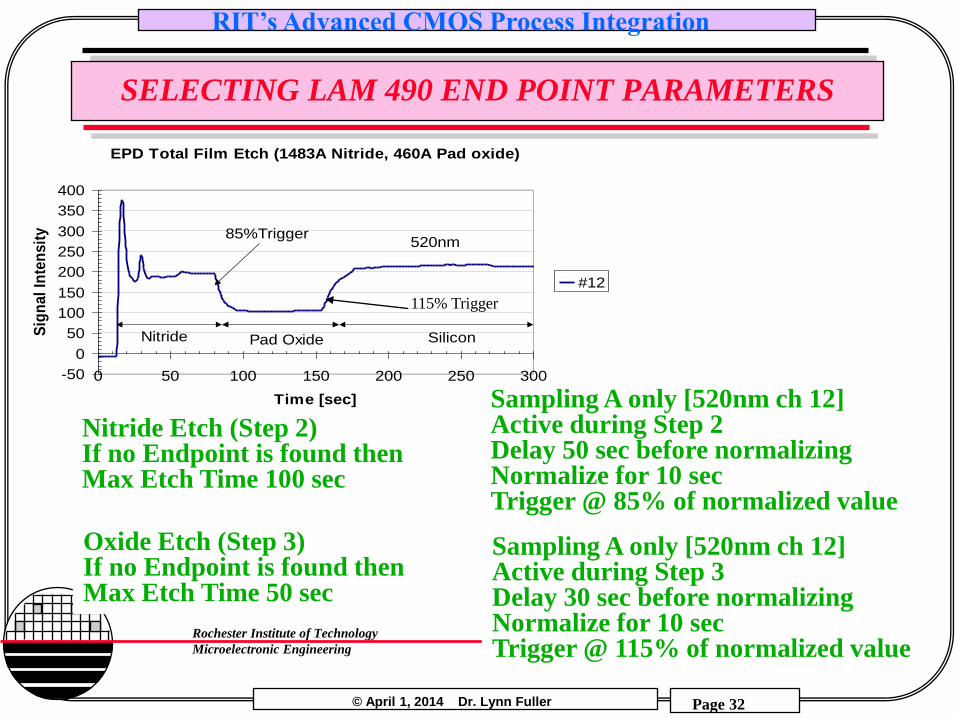
SELECTING LAM 490 END POINT PARAMETERS
EPD Total Film Etch (1483A Nitride, 460A Pad oxide)
-50
0
50
100
150
200
250
300
350
400
0 50 100 150 200 250 300
Time [sec]
Sig
nal
Inte
nsit
y
#12
Nitride Pad Oxide Silicon
85%Trigger520nm
Sampling A only [520nm ch 12] Active during Step 2 Delay 50 sec before normalizing Normalize for 10 sec Trigger @ 85% of normalized value
Nitride Etch (Step 2) If no Endpoint is found then Max Etch Time 100 sec
Sampling A only [520nm ch 12] Active during Step 3 Delay 30 sec before normalizing Normalize for 10 sec Trigger @ 115% of normalized value
115% Trigger
Oxide Etch (Step 3) If no Endpoint is found then Max Etch Time 50 sec

© April 1, 2014 Dr. Lynn Fuller
RIT’s Advanced CMOS Process Integration
Page 33
Rochester Institute of Technology
Microelectronic Engineering
FINALIZE STI ETCH RECIPE
Process: Step 1 – 260mTorr; 0 watts 200sccm SF6, Max Time = 2 min Time Only Process: Step 2 – 260mTorr; 125 watts, 200sccm SF6, Max Time = 1min 40sec Endpoint and Time Sampling A (ch12 @ 520nm) Active during step 02 Delay 50sec before normalizing Normalize for 10sec Trigger at 85%
Process: Step 3 – 260mTorr; 125 watts, 200sccm SF6, Max Time = 50sec Endpoint and Time Sampling A (ch12 @ 520nm) Active during step 03 Delay 30sec before normalizing Normalize for 10sec Trigger at 115% Process: Step 4 – 260mTorr; 125W, 200sccm SF6, Time Only, Max Time = 50 sec

© April 1, 2014 Dr. Lynn Fuller
RIT’s Advanced CMOS Process Integration
Page 34
Rochester Institute of Technology
Microelectronic Engineering
CONTINUE THE ETCH THRU PAD OXIDE AND INTO THE SILICON
Substrate 10 ohm-cm

© April 1, 2014 Dr. Lynn Fuller
RIT’s Advanced CMOS Process Integration
Page 35
Rochester Institute of Technology
Microelectronic Engineering
MEGASONIC RCA CLEAN, SRD & ASHER
Asher
RCA Clean Bench

© April 1, 2014 Dr. Lynn Fuller
RIT’s Advanced CMOS Process Integration
Page 36
Rochester Institute of Technology
Microelectronic Engineering
RECESSED OXIDE GROWTH PROCESS FLOW
§ Grow 500A Pad Oxide (thermal)
§ Deposit 1500A Si3N4 by LPCVD
§ Level 1 Lithography to protect Active areas with photoresist
§ Etch Nitride (Plasma)
Joe Corea 2011

© April 1, 2014 Dr. Lynn Fuller
RIT’s Advanced CMOS Process Integration
Page 37
Rochester Institute of Technology
Microelectronic Engineering
RECESSED OXIED GROWTH PROCESS FLOW
§ Remove Photo Resist
§ Grow First oxide (Thermal) 3650 Å
§ Strip First oxide (Wet)
Joe Corea 2011

© April 1, 2014 Dr. Lynn Fuller
RIT’s Advanced CMOS Process Integration
Page 38
Rochester Institute of Technology
Microelectronic Engineering
RECESSED OXIDE GROWTH PROCESS FLOW
§ Grow second Oxide (Thermal) also 3650 Å
Final oxide growth will give correct depth and
thickness to achieve a phase shift, meet the previous
pad oxide, and satisfy isolation criteria.
Joe Corea 2011

© April 1, 2014 Dr. Lynn Fuller
RIT’s Advanced CMOS Process Integration
Page 39
Rochester Institute of Technology
Microelectronic Engineering
RECESSED OXIDE GROWTH SIMULATION
Simulation Output was
analyzed and
determined to be correct
Joe Corea 2011

© April 1, 2014 Dr. Lynn Fuller
RIT’s Advanced CMOS Process Integration
Page 40
Rochester Institute of Technology
Microelectronic Engineering
HOT PHOSPHORIC ACID NITRIDE ETCH
Substrate 10 ohm-cm
30s Dip in 5:1 BHF, Rinse Hot Phosphoric Acid Wet Nitride Etch. Etch Rate ~80 Å/min Etch ~20 min.
P-well N-well

© April 1, 2014 Dr. Lynn Fuller
RIT’s Advanced CMOS Process Integration
Page 41
Rochester Institute of Technology
Microelectronic Engineering
HOT PHOSPHORIC ACID ETCH BENCH
• Include D1-D3
• Warm up Hot Phos pot to 175º
• Use Teflon boat to place wafers in acid bath
• Etch rate of ~80 Å/min
• Rinse for 5 minutes in Cascade Rinse
• SRD wafers

© April 1, 2014 Dr. Lynn Fuller
RIT’s Advanced CMOS Process Integration
Page 42
Rochester Institute of Technology
Microelectronic Engineering
WELL DRIVE
Substrate 10 ohm-cm
P-well N-well
6 hrs, 1100 °C

© April 1, 2014 Dr. Lynn Fuller
RIT’s Advanced CMOS Process Integration
Page 43
Rochester Institute of Technology
Microelectronic Engineering
BRUCE FURNACE RECIPE 11 ADV-CMOS WELL DRIVE
1100°C
800 °C
Boat Out Boat In Boat Out
Load Push Stabilize Ramp-Up Soak Anneal Ramp-Down Pull
12 min 15 min 30 min 360 min 5 min 60 min 12 min
10 lmp 10 lpm 10 lpm 10 lpm 10 lpm 10 lpm 5 lpm
N2 N2 N2 N2 N2 N2 N2
Recipe #11
Interval 0 Interval 1 Interval 2 Interval 3 Interval 4 Interval 5 Interval 6 Interval 7
800 °C
25 °C
Any
0 lpm
none
800 °C
At the end of a run the furnace returns to Interval 0 which is set for boat out, 25 °C and no gas flow. The furnace waits in that state until someone aborts the current recipe or loads a new recipe.
Adv-CMOS Well Drive, No Oxide Growth, Tube 1

© April 1, 2014 Dr. Lynn Fuller
RIT’s Advanced CMOS Process Integration
Page 44
Rochester Institute of Technology
Microelectronic Engineering
CALCULATION OF NMOS AND PMOS VT ADJUST
Michael Latham, May 2005
Calculate using:
1. Hand Calculations
2. Silvaco Supreme (Athena)

© April 1, 2014 Dr. Lynn Fuller
RIT’s Advanced CMOS Process Integration
Page 45
Rochester Institute of Technology
Microelectronic Engineering
NMOS CALCULATION
ROCHESTER INSTITUTE OF TECHNOLOGY MOSFETVT.XLS FILE3B
MICROELECTRONIC ENGINEERING 12/28/1995
CALCULATION OF MOSFET THRESHOLD VOLTAGE LYNN FULLER
To use this spreadsheet change the values in the white boxes. The rest of the sheet is protected and should not be changed unless
you are sure of the consequences. The calculated results are shown in the purple boxes.
CONSTANTS VARIABLES CHOICES
1=yes, 0=No
T= 300 K Na = 1.00E+17 cm-3 Aluminum gate 0
KT/q = 0.026 volts Nd = 1.00E+17 cm-3 n+ Poly gate 1
ni = 1.45E+10 cm-3 Nss = 1.00E+11 cm-2 p+ Poly gate 0
Eo = 8.85E-14 F/cm Xox = 100 Ang N substrate 0
Er si = 11.7 P substrate 1
Er SiO2 = 3.9
E affinity = 4.15 volts Desired VT 0.75
q = 1.60E-19 coul or
Eg = 1.124 volts Delta VT 20
Given Dose (Boron) 1.30E+12
CALCULATIONS: RESULTS
METAL WORK FUNCTION = 4.122988528 volts
SEMICONDUCTOR POTENTIAL = +/- 0.409409834 volts
OXIDE CAPACITANCE / CM2 = 3.4515E-07 F/cm2 Wdmax = 0.103 µm
METAL SEMI WORK FUNCTION DIFF = -0.998421306 volts
FLAT BAND VOLTAGE = -1.044777963 volts
THRESHOLD VOLTAGE = 0.25126959 volts
DELTA VT = VTdesired - VT = 0.49873041 volts
IMPLANT DOSE = 1.07586E+12 ions/cm2 x 2 = 2.15171E+12
where + is Boron, - is Phosphorous
Select one type of gate
Select one type of substrate

© April 1, 2014 Dr. Lynn Fuller
RIT’s Advanced CMOS Process Integration
Page 46
Rochester Institute of Technology
Microelectronic Engineering
PMOS CALCULATION
ROCHESTER INSTITUTE OF TECHNOLOGY MOSFETVT.XLS FILE3B
MICROELECTRONIC ENGINEERING 12/28/1995
CALCULATION OF MOSFET THRESHOLD VOLTAGE LYNN FULLER
To use this spreadsheet change the values in the white boxes. The rest of the sheet is protected and should not be changed unless
you are sure of the consequences. The calculated results are shown in the purple boxes.
CONSTANTS VARIABLES CHOICES
1=yes, 0=No
T= 300 K Na = 1.00E+17 cm-3 Aluminum gate 0
KT/q = 0.026 volts Nd = 1.00E+17 cm-3 n+ Poly gate 0
ni = 1.45E+10 cm-3 Nss = 1.00E+11 cm-2 p+ Poly gate 1
Eo = 8.85E-14 F/cm Xox = 100 Ang N substrate 1
Er si = 11.7 P substrate 0
Er SiO2 = 3.9
E affinity = 4.15 volts Desired VT -0.75
q = 1.60E-19 coul or
Eg = 1.124 volts Delta VT 20
Given Dose (Boron) 1.30E+12
CALCULATIONS: RESULTS
METAL WORK FUNCTION = 5.301011472 volts
SEMICONDUCTOR POTENTIAL = +/- 0.409409834 volts
OXIDE CAPACITANCE / CM2 = 3.4515E-07 F/cm2 Wdmax = 0.103 µm
METAL SEMI WORK FUNCTION DIFF = 0.998421306 volts
FLAT BAND VOLTAGE = 0.95206465 volts
THRESHOLD VOLTAGE = -0.343982903 volts
DELTA VT = VTdesired - VT = -0.406017097 volts
IMPLANT DOSE = -8.75855E+11 ions/cm2 x 2 = -1.75171E+12
where + is Boron, - is Phosphorous
Select one type of gate
Select one type of substrate

© April 1, 2014 Dr. Lynn Fuller
RIT’s Advanced CMOS Process Integration
Page 47
Rochester Institute of Technology
Microelectronic Engineering
NMOS SIMULATIONS
Id-Vg
VT = 0.61V VT Adjust Implant: None
Id-Vg
VT = 0.73V VT Adjust Implant: B11, 30KeV, Dose 3.0E12 cm-2

© April 1, 2014 Dr. Lynn Fuller
RIT’s Advanced CMOS Process Integration
Page 48
Rochester Institute of Technology
Microelectronic Engineering
PMOS SIMULATIONS
Id-Vg
VT = -0.31V
VT Adjust Implant: None
Id-Vg
VT = -0.74V
VT Adjust Implant: P31, 60KeV, Dose 3.5E12 cm-2

© April 1, 2014 Dr. Lynn Fuller
RIT’s Advanced CMOS Process Integration
Page 49
Rochester Institute of Technology
Microelectronic Engineering
RESULTS OF CALCULATIONS AND SIMULATIONS
NMOS Desired 0.75, with No Adjust 0.61
From SUPREM 3.0E12 @30 KeV Boron B11
From Hand Calculations 2.15E12
PMOS Desired -0.75, with No Adjust -0.31
From SUPREM 3.5E12 @ 60KeV Phosphorous P31
From Hand Calculations 1.8E12

© April 1, 2014 Dr. Lynn Fuller
RIT’s Advanced CMOS Process Integration
Page 50
Rochester Institute of Technology
Microelectronic Engineering
PHOTO - NMOS VT ADJUST
Substrate 10 ohm-cm
P-well N-well

© April 1, 2014 Dr. Lynn Fuller
RIT’s Advanced CMOS Process Integration
Page 51
Rochester Institute of Technology
Microelectronic Engineering
NMOS VT ADJUST IMPLANT
3.0e12, 30keV, B11
Substrate 10 ohm-cm
P-well N-well

© April 1, 2014 Dr. Lynn Fuller
RIT’s Advanced CMOS Process Integration
Page 52
Rochester Institute of Technology
Microelectronic Engineering
PHOTO PMOS VT ADJUST
Substrate 10 ohm-cm
P-well N-well

© April 1, 2014 Dr. Lynn Fuller
RIT’s Advanced CMOS Process Integration
Page 53
Rochester Institute of Technology
Microelectronic Engineering
PMOS VT IMPLANT
3.5E12, 60keV, P31
Substrate 10 ohm-cm
P-well N-well

© April 1, 2014 Dr. Lynn Fuller
RIT’s Advanced CMOS Process Integration
Page 54
Rochester Institute of Technology
Microelectronic Engineering
STRIP RESIST
Substrate 10 ohm-cm
P-well N-well

© April 1, 2014 Dr. Lynn Fuller
RIT’s Advanced CMOS Process Integration
Page 55
Rochester Institute of Technology
Microelectronic Engineering
OXIDE ETCH
Substrate 10 ohm-cm
P-well N-well
Etch in 10:1 BOE
45 seconds, Rinse, SRD

© April 1, 2014 Dr. Lynn Fuller
RIT’s Advanced CMOS Process Integration
Page 56
Rochester Institute of Technology
Microelectronic Engineering
RCA CLEAN AND GROW GATE OXIDE
Just Prior to Gate Oxide Growth
Etch wafers in 50:1 HF, 1 min.
Grow Oxide, 100Å, Dry O2
Bruce Furnace04 Recipe 213
Substrate 10 ohm-cm
P-well N-well

© April 1, 2014 Dr. Lynn Fuller
RIT’s Advanced CMOS Process Integration
Page 57
Rochester Institute of Technology
Microelectronic Engineering
INCORPORATING NITROGEN IN THIN GATE OXIDES
In todays deep sub-micron transistors the pMOSFET normally has p+Poly for the gate material. The gate oxide is 100Å or less. The p+ dopant is normally Boron and Boron diffuses quickly (compared to Phosphorous) through oxides. Since the gate oxides are thin this could allow Boron to diffuse through the gate oxide and dope the channel causing the transistors to not function correctly. If some nitrogen is incorporated in the gate oxide the diffusion of Boron is much lower. This project involved developing a gate oxide recipe that will result in nitrogen incorporation in the gate oxide. The recipe included 30 min anneal in N2, 30 min oxynitride growth in N2O and 30 min oxide growth in O2, all at 900 °C. The gate oxides were evaluated at RIT using the ellipsometer (looking for index of refraction in between 1.45 (oxide) and 2.00 (nitride) and thickness near 100Å. The same wafers were also sent to Kodak for XPS analysis to give information on nitrogen content in the oxide.

© April 1, 2014 Dr. Lynn Fuller
RIT’s Advanced CMOS Process Integration
Page 58
Rochester Institute of Technology
Microelectronic Engineering
BRUCE FURNACE RECIPE 213
900°C
800 °C
Boat Out Boat In Boat Out
Load Push Stabilize Ramp-Up Soak Soak Ramp-Down Pull
12 min 30 min 30 min 30min 30 min 30 min 15 min
5 lpm 5 lmp 10 lpm 10 lpm 10 lpm 10 lpm 5 lpm
N2 N2 O2 N2O O2 N2 N2
Recipe #213
Interval 0 Interval 1 Interval 2 Interval 3 Interval 4 Interval 5 Interval 6 Interval 7
Dry Oxide Growth with N2O, Target 100 Å
800 °C
25 °C
Any
0 lpm
none
800 °C
At the end of a run the furnace returns to Interval 0 which is set for boat out, 25 °C and no gas flow. The furnace waits in that state until someone aborts the current recipe or loads a new recipe.

© April 1, 2014 Dr. Lynn Fuller
RIT’s Advanced CMOS Process Integration
Page 59
Rochester Institute of Technology
Microelectronic Engineering
INCORPORATING NITROGEN IN THIN GATE OXIDES
XPS Compositional Depth Profiles of SiOXNY
0
20
40
60
80
100
0 50 100 150 200
Sputter time (S)
Ato
m %
Si,
O,
C
0
0.2
0.4
0.6
0.8
1
Ato
m %
N
%Si
%O
%C
%N
Si
O N
0 100 Å

© April 1, 2014 Dr. Lynn Fuller
RIT’s Advanced CMOS Process Integration
Page 60
Rochester Institute of Technology
Microelectronic Engineering
LOCATION FOR MEASUREMENT OF GATE OXIDE
Measure gate oxide thickness (~100A) in any white active area

© April 1, 2014 Dr. Lynn Fuller
RIT’s Advanced CMOS Process Integration
Page 61
Rochester Institute of Technology
Microelectronic Engineering
Login: FACTORY Password: OPER <F1> Operate <F1> Test Center the wafer on the stage Select (use arrow keys on the numeric pad (far right on the keyboard) space bar, page up, etc) PROGRAM = FAC-P or FAC-N LOT ID = HAWAII WAFER NO. = C1 TOX = 250 (from nanospec) <F12> start test and wait for measurement <Print Screen> print results <F8> exit and log off <ESC> can be used anytime, but wait for current test to be completed
MEASURE GATE OXIDE ON SCA-2500

© April 1, 2014 Dr. Lynn Fuller
RIT’s Advanced CMOS Process Integration
Page 62
Rochester Institute of Technology
Microelectronic Engineering
SCA MEASUREMENT OF GATE OXIDE

© April 1, 2014 Dr. Lynn Fuller
RIT’s Advanced CMOS Process Integration
Page 63
Rochester Institute of Technology
Microelectronic Engineering
LPCVD POLY
Polysilicon, 4000A
LPCVD, 610C, ~55min
100 sccm of SiH4, 300 mTorr
Substrate 10 ohm-cm
P-well N-well

© April 1, 2014 Dr. Lynn Fuller
RIT’s Advanced CMOS Process Integration
Page 64
Rochester Institute of Technology
Microelectronic Engineering
LOCATION FOR POLY THICKNESS MEASUREMENT
Measure poly thickness within any active area using thin film
stack #4 on nanospec at 40X magnification

© April 1, 2014 Dr. Lynn Fuller
RIT’s Advanced CMOS Process Integration
Page 65
Rochester Institute of Technology
Microelectronic Engineering
PHOTO 6 POLY GATE
Substrate 10 ohm-cm
P-well N-well

© April 1, 2014 Dr. Lynn Fuller
RIT’s Advanced CMOS Process Integration
Page 66
Rochester Institute of Technology
Microelectronic Engineering
POLY ETCH
Substrate 10 ohm-cm
P-well N-well
old

© April 1, 2014 Dr. Lynn Fuller
RIT’s Advanced CMOS Process Integration
Page 67
Rochester Institute of Technology
Microelectronic Engineering
DRYTEK QUAD RIE TOOL

© April 1, 2014 Dr. Lynn Fuller
RIT’s Advanced CMOS Process Integration
Page 68
Rochester Institute of Technology
Microelectronic Engineering
2 OF 4 CHAMBERS IN THE DRYTEK QUAD RIE TOOL

© April 1, 2014 Dr. Lynn Fuller
RIT’s Advanced CMOS Process Integration
Page 69
Rochester Institute of Technology
Microelectronic Engineering
PLASMA ETCHING IN THE DRYTEK QUAD

© April 1, 2014 Dr. Lynn Fuller
RIT’s Advanced CMOS Process Integration
Page 70
Rochester Institute of Technology
Microelectronic Engineering
ANISOTROPIC POLY GATE ETCH RECIPE
Anisotropic Poly Gate Etch Recipe
SF6 30 sccm, CHF3 30 sccm, O2 5 sccm, RF Power 160 w, Pressure 40 mTorr,
1900 A/min (Anisotropic), Resist Etch Rate 300 A/min, Oxide Etch Rate 200 A/min Recipe Name: FACPOLY Step 2 Chamber 2 Power 160 watts Pressure 40 mTorr Gas SF6 Flow 30 sccm Gas CHF3 Flow 30 sccm Gas O2 Flow 5 sccm Poly Etch Rate 1150 Å/min Photoresist Etch Rate: 300 Å/min Oxide Etch Rate: 200 Å/min
Endpoint See Video
http://people.rit.edu/lffeee/videos.htm

© April 1, 2014 Dr. Lynn Fuller
RIT’s Advanced CMOS Process Integration
Page 71
Rochester Institute of Technology
Microelectronic Engineering
VERIFICATION
Resist
Poly
Oxide
200nm
500 Å 250 Å 3000 Å
6000 Å
New Pictures

© April 1, 2014 Dr. Lynn Fuller
RIT’s Advanced CMOS Process Integration
Page 72
Rochester Institute of Technology
Microelectronic Engineering
STRIP RESIST
P-well N-well
Include D1-D3 Strip Photresist in Branson Asher

© April 1, 2014 Dr. Lynn Fuller
RIT’s Advanced CMOS Process Integration
Page 73
Rochester Institute of Technology
Microelectronic Engineering
RCA CLEAN
P-well N-well

© April 1, 2014 Dr. Lynn Fuller
RIT’s Advanced CMOS Process Integration
Page 74
Rochester Institute of Technology
Microelectronic Engineering
POLY REOX OXIDE
P-well N-well
Oxide, 500A
Bruce Furnace 04 Recipe 250
~45 min at 1000 °C

© April 1, 2014 Dr. Lynn Fuller
RIT’s Advanced CMOS Process Integration
Page 75
Rochester Institute of Technology
Microelectronic Engineering
PHOTO 7 LDD P-TYPE IMPLANT
Substrate 10 ohm-cm
P-well N-well

© April 1, 2014 Dr. Lynn Fuller
RIT’s Advanced CMOS Process Integration
Page 76
Rochester Institute of Technology
Microelectronic Engineering
IMPLANT P-LDD
Substrate 10 ohm-cm
P-well N-well
B11, Dose = 4E13, E = 50 KeV

© April 1, 2014 Dr. Lynn Fuller
RIT’s Advanced CMOS Process Integration
Page 77
Rochester Institute of Technology
Microelectronic Engineering
IMPLANT MASKING THICKNESS CALCULATOR
Rochester Institute of Technology Lance Barron
Microelectronic Engineering Dr. Lynn Fuller
11/20/04
IMPLANT MASK CALCULATOR Enter 1 - Yes 0 - No in white boxes
DOPANT SPECIES MASK TYPE ENERGY
B11 1 Resist 0 50 KeV
BF2 0 Poly 1
P31 0 Oxide 0
Nitride 0
Thickness to Mask >1E15/cm3 Surface Concentration 3529.481 Angstroms

© April 1, 2014 Dr. Lynn Fuller
RIT’s Advanced CMOS Process Integration
Page 78
Rochester Institute of Technology
Microelectronic Engineering
STRIP RESIST
P-well N-well
Include D1-D3 Strip Photresist in Branson Asher

© April 1, 2014 Dr. Lynn Fuller
RIT’s Advanced CMOS Process Integration
Page 79
Rochester Institute of Technology
Microelectronic Engineering
PHOTO 8 LDD N-TYPE IMPLANT
Substrate 10 ohm-cm
P-well N-well

© April 1, 2014 Dr. Lynn Fuller
RIT’s Advanced CMOS Process Integration
Page 80
Rochester Institute of Technology
Microelectronic Engineering
IMPLANT N-LDD
Substrate 10 ohm-cm
P-well N-well
P31, Dose = 4E13, E = 60 KeV

© April 1, 2014 Dr. Lynn Fuller
RIT’s Advanced CMOS Process Integration
Page 81
Rochester Institute of Technology
Microelectronic Engineering
IMPLANT MASKING THICKNESS CALCULATOR
Rochester Institute of Technology Lance Barron
Microelectronic Engineering Dr. Lynn Fuller
11/20/04
IMPLANT MASK CALCULATOR Enter 1 - Yes 0 - No in white boxes
DOPANT SPECIES MASK TYPE ENERGY
B11 0 Resist 0 60 KeV
BF2 0 Poly 1
P31 1 Oxide 0
Nitride 0
Thickness to Mask >1E15/cm3 Surface Concentration 2798.861 Angstroms

© April 1, 2014 Dr. Lynn Fuller
RIT’s Advanced CMOS Process Integration
Page 82
Rochester Institute of Technology
Microelectronic Engineering
STRIP RESIST
P-well N-well
Include D1-D3 Strip Photresist in Branson Asher

© April 1, 2014 Dr. Lynn Fuller
RIT’s Advanced CMOS Process Integration
Page 83
Rochester Institute of Technology
Microelectronic Engineering
RCA CLEAN AND LPCVD NITRIDE
ASM 6” LPCVD Tool
Target 3500 Å
P-well N-well
LPCVD Nitride 810°C
400 mTorr, NH3 flow = 150 sccm
Dichlorosilane flow = 60 sccm

© April 1, 2014 Dr. Lynn Fuller
RIT’s Advanced CMOS Process Integration
Page 84
Rochester Institute of Technology
Microelectronic Engineering
NITRIDE SIDE WALL SPACERS
Power 250 Watts
Pressure 40 mTorr
SF6 30 sccm
CHF3 30 sccm
Nitride Etch Rate 1250 A/min
Nitride Etch %NU ~ 4% *
Oxide Etch Rate ~ 950 A/min *
Oxide Etch %NU ~ 10% *
Selectivity Nitride:Oxide 1.3:1
Nitride as a side wall spacer in deep sub micron transistor fabrication has some advantages over oxide side wall spacers. Nitride LPCVD is a more uniform and more conformal film than LTO. Nitride offers the possibility of end-point detection and higher selectivity during the plasma etch, while an oxide spacer does not.
Side Wall Spacer
Ion Implant
Dry
tek Q
uad

© April 1, 2014 Dr. Lynn Fuller
RIT’s Advanced CMOS Process Integration
Page 85
Rochester Institute of Technology
Microelectronic Engineering
NITRIDE SIDE WALL SPACERS
Poly thickness = 2300 A
Oxide thickness = 1000A
Spacer Height = 2300 A
Spacer Width = 0.3 um
Special thanks to
Dr. Sean Rommel for
help in using the new
LEO SEM

© April 1, 2014 Dr. Lynn Fuller
RIT’s Advanced CMOS Process Integration
Page 86
Rochester Institute of Technology
Microelectronic Engineering
SIDE WALL SPACER ETCH IN DRYTEK QUAD
Anisotropic Nitride Etch Drytek Quad Recipe FACSPCR 30 sccm SF6 30 sccm CHF3 Power = 200 watts Pressure = 50 mTorr Etch Rate = 125 nm/min

© April 1, 2014 Dr. Lynn Fuller
RIT’s Advanced CMOS Process Integration
Page 87
Rochester Institute of Technology
Microelectronic Engineering
AFTER ETCH NITRIDE TO FORM SIDE WALL SPACERS
P-well N-well

© April 1, 2014 Dr. Lynn Fuller
RIT’s Advanced CMOS Process Integration
Page 88
Rochester Institute of Technology
Microelectronic Engineering
PHOTO 9 N+ D/S
P-well N-well
P31, Dose = 4 E15, E = 60 KeV

© April 1, 2014 Dr. Lynn Fuller
RIT’s Advanced CMOS Process Integration
Page 89
Rochester Institute of Technology
Microelectronic Engineering
IMPLANT MASKING THICKNESS CALCULATOR
Rochester Institute of Technology Lance Barron
Microelectronic Engineering Dr. Lynn Fuller
11/20/04
IMPLANT MASK CALCULATOR Enter 1 - Yes 0 - No in white boxes
DOPANT SPECIES MASK TYPE ENERGY
B11 0 Resist 0 60 KeV
BF2 0 Poly 1
P31 1 Oxide 0
Nitride 0
Thickness to Mask >1E15/cm3 Surface Concentration 2798.861 Angstroms

© April 1, 2014 Dr. Lynn Fuller
RIT’s Advanced CMOS Process Integration
Page 90
Rochester Institute of Technology
Microelectronic Engineering
STRIP RESIST
P-well N-well
Include D1-D3 Strip Photresist in Branson Asher

© April 1, 2014 Dr. Lynn Fuller
RIT’s Advanced CMOS Process Integration
Page 91
Rochester Institute of Technology
Microelectronic Engineering
PHOTO 10 P+ D/S
P-well N-well

© April 1, 2014 Dr. Lynn Fuller
RIT’s Advanced CMOS Process Integration
Page 92
Rochester Institute of Technology
Microelectronic Engineering
IMPLANT P+ D/S
B11, Dose = 4 E15, E = 50 KeV
P-well N-well

© April 1, 2014 Dr. Lynn Fuller
RIT’s Advanced CMOS Process Integration
Page 93
Rochester Institute of Technology
Microelectronic Engineering
IMPLANT MASKING THICKNESS CALCULATOR
Rochester Institute of Technology Lance Barron
Microelectronic Engineering Dr. Lynn Fuller
11/20/2004
IMPLANT MASK CALCULATOR Enter 1 - Yes 0 - No in white boxes
DOPANT SPECIES MASK TYPE ENERGY
B11 1 Resist 0 50 KeV
BF2 0 Poly 1
P31 0 Oxide 0
Nitride 0
Thickness to Mask >1E15/cm3 Surface Concentration 3529.481 Angstroms

© April 1, 2014 Dr. Lynn Fuller
RIT’s Advanced CMOS Process Integration
Page 94
Rochester Institute of Technology
Microelectronic Engineering
STRIP RESIST, RCA CLEAN
P-well N-well
Include D1-D3 Strip Photresist in Branson Asher

© April 1, 2014 Dr. Lynn Fuller
RIT’s Advanced CMOS Process Integration
Page 95
Rochester Institute of Technology
Microelectronic Engineering
BRUCE FURNACE RECIPE 284 – Adv-CMOS ANNEAL
1000°C
800 °C
Boat Out Boat In Boat Out
Load Push Stabilize Ramp-Up Soak Anneal Ramp-Down Pull
12 min 15 min 20 min 20 min 5 min 40 min 15 min
10 lpm 10 lmp 5 lpm 10 lpm 15 lpm 10 lpm 5 lpm
N2 N2 N2 N2 N2 N2 N2
Recipe #284
Interval 0 Interval 1 Interval 2 Interval 3 Interval 4 Interval 5 Interval 6 Interval 7
800 °C
25 °C
Any
0 lpm
none
800 °C
At the end of a run the furnace returns to Interval 0 which is set for boat out, 25 °C and no gas flow. The furnace waits in that state until someone aborts the current recipe or loads a new recipe.
DS Implant Anneal, Oxide Growth

© April 1, 2014 Dr. Lynn Fuller
RIT’s Advanced CMOS Process Integration
Page 96
Rochester Institute of Technology
Microelectronic Engineering
ETCH OXIDE
P-well N-well

© April 1, 2014 Dr. Lynn Fuller
RIT’s Advanced CMOS Process Integration
Page 97
Rochester Institute of Technology
Microelectronic Engineering
TiSi SALACIDE PROCESS
Forming a metal silicide helps reduce the resistance of the polysilicon interconnects and reduces the sheet resistance of the drain/source areas of the transistor. In deep sub-micron CMOS the nMOSFET transistor has n+ poly and the pMOSFET has p+ poly. Normally the poly is doped by ion implantation at the same time the drain and sources is implanted. In this case it is essential to form a silicide to reduce the sheet resistance of the poly and to connect n+ and p+ poly where ever they meet. SALICIDE is an acronym for self-aligned silicide and can be achieved with the following process. Ti (or some other metal) is sputtered on the wafer. It is heated in vacuum or N2 atmosphere to form TiSi where ever the Ti metal is in contact with silicon but not where it is in contact with silicon dioxide. The wafer is etched in sulfuric acid and hydrogen peroxide mixture which removes the metal from the oxide regions leaving TiSi self aligned on the silicon areas. Further heat treating at a higher temperature can convert TiSi to TiSi2 which is lower sheet resistance.

© April 1, 2014 Dr. Lynn Fuller
RIT’s Advanced CMOS Process Integration
Page 98
Rochester Institute of Technology
Microelectronic Engineering
TiSi SALACIDE PROCESS
Sputtering of Titanium: Dip in 50:1 HF, Spin Rinse Dry Just prior to metal deposition. Ti Thickness = 1000Å 4” Target, 350 watts, 5 mTorr, 5 min pre-sputter, 10 min sputter, Rate = 100Å/min 8” Target, 750 watts, 5 mTorr, 5 min pre-sputter, 6 min sputter, Rate = ~176 Å/min
Heater time, 20 min., 300 C Base Pressure <5E-6 Torr

© April 1, 2014 Dr. Lynn Fuller
RIT’s Advanced CMOS Process Integration
Page 99
Rochester Institute of Technology
Microelectronic Engineering
AFTER Ti SPUTTER
P-well N-well

© April 1, 2014 Dr. Lynn Fuller
RIT’s Advanced CMOS Process Integration
Page 100
Rochester Institute of Technology
Microelectronic Engineering
RTP TO FORM SILICIDE
P-well N-well
AG Associates 610 N2 Recipe TISI1.RCP Temp = ~650 C Time = 1 min.

© April 1, 2014 Dr. Lynn Fuller
RIT’s Advanced CMOS Process Integration
Page 101
Rochester Institute of Technology
Microelectronic Engineering
ETCH REMOVE Ti
P-well N-well
Mix new chemicals in 9”x9” Pyrex Dish Use hot plate set to 150 C but etch at 90 C H2S04:H2O2 (1:2), Temp ~90C (self heating) Etch Time = 2 min Rinse, 5 min., Spin-Rinse Dry

© April 1, 2014 Dr. Lynn Fuller
RIT’s Advanced CMOS Process Integration
Page 102
Rochester Institute of Technology
Microelectronic Engineering
TiSi SALACIDE PROCESS
Courtesy of SMFL
Etching of Ti Metal: Heat the Sulfuric Acid:Hydrogen Peroxide (1:2) mixture on a hotplate at 90°C (set plate temperature to 150°C) Etch for 1 min 30 sec. This should remove the Ti that is on top of the silicon dioxide but not remove TiSi that was formed on the polysilicon and D/S regions. It also removes unreacted Ti metal over the TiSi on the poly and D/S regions.

© April 1, 2014 Dr. Lynn Fuller
RIT’s Advanced CMOS Process Integration
Page 103
Rochester Institute of Technology
Microelectronic Engineering
AG Associates 610 N2 Recipe TiSi2.RCP Temp = ~800 C Time = 1 min.
RTP TO FORM SILICIDE (TiSi2)
P-well N-well

© April 1, 2014 Dr. Lynn Fuller
RIT’s Advanced CMOS Process Integration
Page 104
Rochester Institute of Technology
Microelectronic Engineering
RCA CLEAN AND DEPOSIT LPCVD OXIDE
Target 4000 Å
P-well N-well

© April 1, 2014 Dr. Lynn Fuller
RIT’s Advanced CMOS Process Integration
Page 105
Rochester Institute of Technology
Microelectronic Engineering
PECVD OXIDE FROM TEOS
TEOS Program: (Chamber A) Step 1 Setup Time = 15 sec Pressure = 9 Torr Susceptor Temperature= 390 C Susceptor Spacing= 220 mils RF Power = 0 watts TEOS Flow = 400 scc O2 Flow = 285 scc Step 2 – Deposition Dep Time = 55 sec (5000 Å) Pressure = 9 Torr Susceptor Temperature= 390 C Susceptor Spacing= 220 mils RF Power = 205 watts TEOS Flow = 400 scc O2 Flow = 285 scc Step 3 – Clean Time = 10 sec Pressure = Fully Open Susceptor Temperature= 390 C Susceptor Spacing= 999 mils RF Power = 50 watts TEOS Flow = 0 scc O2 Flow = 285 scc

© April 1, 2014 Dr. Lynn Fuller
RIT’s Advanced CMOS Process Integration
Page 106
Rochester Institute of Technology
Microelectronic Engineering
PHOTO 11 CONTACT CUTS
P-well N-well
Increase Dose and Develop Time Exposure Dose 185 mj/cm2 Use DEVFAC.RCP

© April 1, 2014 Dr. Lynn Fuller
RIT’s Advanced CMOS Process Integration
Page 107
Rochester Institute of Technology
Microelectronic Engineering
ETCH CONTACT CUTS
P-well N-well
Plasma Etch Using FACCUT in Drytek Quad 200 Watt, 100 mTorr 50 sccm CHF3, 10 sccm CF4 100 sccm Ar

© April 1, 2014 Dr. Lynn Fuller
RIT’s Advanced CMOS Process Integration
Page 108
Rochester Institute of Technology
Microelectronic Engineering
DRYTEK QUAD ETCH RECIPE FOR CC AND VIA
Recipe Name: FACCUT Chamber 3 Power 200W Pressure 100 mTorr Gas 1 CHF3 50 sccm Gas 2 CF4 10 sccm Gas 3 Ar 100 sccm Gas 4 O2 0 sccm (could be changed to N2) TEOS Etch Rate 494 Å/min Annealed TEOS 450 Å/min Photoresist Etch Rate: 117 Å/min Thermal Oxide Etch Rate: 441 Å/min Silicon Etch Rate 82 Å/min TiSi2 Etch Rate 1 Å/min
US Patent 5935877 - Etch process for forming contacts over titanium silicide
Drytek Quad

© April 1, 2014 Dr. Lynn Fuller
RIT’s Advanced CMOS Process Integration
Page 109
Rochester Institute of Technology
Microelectronic Engineering
FACCCUT RECIPE

© April 1, 2014 Dr. Lynn Fuller
RIT’s Advanced CMOS Process Integration
Page 110
Rochester Institute of Technology
Microelectronic Engineering
CONTACT CUT ETCH RECIPE
Theory: The CHF3 and CF4 provide the F radicals that do the etching of the silicon dioxide, SiO2. The high voltage RF power creates a plasma and the gasses in the chamber are broken into radicals and ions. The F radical combines with Si to make SiF4 which is volatile and is removed by pumping. The O2 in the oxide is released and also removed by pumping. The C and H can be removed as CO, CO2, H2 or other volatile combinations. The C and H can also form hydrocarbon polymers that can coat the chamber and wafer surfaces. The Ar can be ionized in the plasma and at low pressures can be accelerated toward the wafer surface without many collisions giving some vertical ion bombardment on the horizontal surfaces. If everything is correct (wafer temperature, pressure, amounts of polymer formed, energy of Ar bombardment, etc.) the SiO2 should be etched, polymer should be formed on the horizontal and vertical surfaces but the Ar bombardment on the horizontal surfaces should remove the polymer there. The O2 (O radicals) released also help remove polymer. Once the SiO2 is etched and the underlying Si is reached there is less O2 around and the removal of polymer on the horizontal surfaces is not adequate thus the removal rate of the Si is reduced. The etch rate of SiO2 should be 4 or 5 times the etch rate of the underlying Si. The chamber should be cleaned in an O2 plasma after each wafer is etched.
US Patent 5935877 - Etch process for forming contacts over Titanium Silicide

© April 1, 2014 Dr. Lynn Fuller
RIT’s Advanced CMOS Process Integration
Page 111
Rochester Institute of Technology
Microelectronic Engineering
STRIP RESIST
P-well N-well
Include D1-D3 Strip Photresist in Branson Asher

© April 1, 2014 Dr. Lynn Fuller
RIT’s Advanced CMOS Process Integration
Page 112
Rochester Institute of Technology
Microelectronic Engineering
RCA CLEAN
DI water rinse, 5 min.
H20 - 50 HF - 1 60 sec.
HPM HCL - 1part
H2O2 - 3parts H2O - 15parts 70 °C, 15 min.
APM NH4OH - 1part H2O2 - 3parts H2O - 15parts 70 °C, 15 min.
DI water rinse, 5 min.
DI water rinse, 5 min.
H20 - 50 HF - 1 60 sec.
Clean includes 50:1 HF Dip twice once after each bath to remove chemically grown oxide
SPIN/RINSE DRY
DI water rinse, 5 min.

© April 1, 2014 Dr. Lynn Fuller
RIT’s Advanced CMOS Process Integration
Page 113
Rochester Institute of Technology
Microelectronic Engineering
LPCVD TUNGSTEN PLUGS
P-well N-well

© April 1, 2014 Dr. Lynn Fuller
RIT’s Advanced CMOS Process Integration
Page 114
Rochester Institute of Technology
Microelectronic Engineering
DEPOSIT ALUMINUM
0.75 µm Aluminum
CVC 601 Sputter Tool
P-well N-well

© April 1, 2014 Dr. Lynn Fuller
RIT’s Advanced CMOS Process Integration
Page 115
Rochester Institute of Technology
Microelectronic Engineering
PHOTO 12 METAL ONE
P-well N-well
§ Coat (Recipe: COATMTL.RCP) § 400RPM for 2 seconds § 2000RPM for 30 seconds § Thickness of 13127A
§ Exposure § Energy: 140mJ/cm2 § Focus: 0.24um
§ Develop (Recipe: DEVMTL.RCP) § Dispense 7 seconds § Wait 68 seconds § Hard Bake 2 min.

© April 1, 2014 Dr. Lynn Fuller
RIT’s Advanced CMOS Process Integration
Page 116
Rochester Institute of Technology
Microelectronic Engineering
ALUMINUM ETCH USING LAM4600
LAM4600

© April 1, 2014 Dr. Lynn Fuller
RIT’s Advanced CMOS Process Integration
Page 117
Rochester Institute of Technology
Microelectronic Engineering
INTRODUCTION
The LAM4600 is a Reactive Ion Etch (RIE) Tool for Anisotropic Aluminum Plasma Etch. It is a load lock vacuum system to keep room air out of the main etch chamber. The entire system is heated slightly above room temperature because the byproducts of the etch (Aluminum/Chlorides) are volatile and can be pumped out of the chamber but at a slightly lower temperature the byproducts will deposit on the inside surfaces of the tool, pump lines, and pumps. The Gas Reactor Column (GRC) removes the chlorine byproducts from the gas that is exhausted to the outside world. Endpoint detection is available and is based on plasma brightness (similar to the LAM490 tool) Other materials can be etched with these chemicals. The tool has a built in water rinse station at the exit that can be used (or not) to reduce chlorine residue on the wafers. We do an external SRD rinse on the wafers after etching.

© April 1, 2014 Dr. Lynn Fuller
RIT’s Advanced CMOS Process Integration
Page 118
Rochester Institute of Technology
Microelectronic Engineering
LAM 4600 ALUMINUM ETCHER
Aluminum Plasma Etch Chemistry
Cl2 – Reduces Pure Aluminum
BCl3 – Etches native Aluminum Oxide
-Increases Physical Sputtering
N2 – Dilute and Carrier for the chemistry
Chloroform – Helps Anisotropy and reduces
photoresist damage

© April 1, 2014 Dr. Lynn Fuller
RIT’s Advanced CMOS Process Integration
Page 119
Rochester Institute of Technology
Microelectronic Engineering
LAM4600 ANISOTROPIC ALUMINUM ETCH
Step 1 2 3 4 5
Pressure 100 100 100 100 0
RF Top (W) 0 0 0 0 0
RF Bottom 0 250 125 125 0
Gap (cm) 3 3 3 3 5.3
O2 111 0 0 0 0 0
N2 222 13 13 20 25 25
BCl 333 50 50 25 25 0
Cl2 444 10 10 30 23 0
Ar 555 0 0 0 0 0
CFORM 666 8 8 8 8 8
Complete Stabl Time Time Oetch Time
Time (s) 15 8 200 10% 15
Fuller April 2013 – 200s
Fuller, January 2012 -300s
Fuller, March 2011 -230s
Channel B
Delay 130
Normalize 10 s
Norm Val 5670
Trigger 105%
Slope +
Rate ~38Å/s Thickness = 7500Å
Various tool modifications
resulted in different etch
rates for different years
Endpoint (not used)

© April 1, 2014 Dr. Lynn Fuller
RIT’s Advanced CMOS Process Integration
Page 120
Rochester Institute of Technology
Microelectronic Engineering
ALUMINUM ETCH
P-well N-well

© April 1, 2014 Dr. Lynn Fuller
RIT’s Advanced CMOS Process Integration
Page 121
Rochester Institute of Technology
Microelectronic Engineering
RESIST STRIP
P-well N-well

© April 1, 2014 Dr. Lynn Fuller
RIT’s Advanced CMOS Process Integration
Page 122
Rochester Institute of Technology
Microelectronic Engineering
LTO
P-well N-well

© April 1, 2014 Dr. Lynn Fuller
RIT’s Advanced CMOS Process Integration
Page 123
Rochester Institute of Technology
Microelectronic Engineering
PECVD OXIDE FROM TEOS
TEOS Program: (Chamber A) Step 1 Setup Time = 15 sec Pressure = 9 Torr Susceptor Temperature= 390 C Susceptor Spacing= 220 mils RF Power = 0 watts TEOS Flow = 400 scc O2 Flow = 285 scc Step 2 – Deposition Dep Time = 55 sec (5000 Å) Pressure = 9 Torr Susceptor Temperature= 390 C Susceptor Spacing= 220 mils RF Power = 205 watts TEOS Flow = 400 scc O2 Flow = 285 scc Step 3 – Clean Time = 10 sec Pressure = Fully Open Susceptor Temperature= 390 C Susceptor Spacing= 999 mils RF Power = 50 watts TEOS Flow = 0 scc O2 Flow = 285 scc

© April 1, 2014 Dr. Lynn Fuller
RIT’s Advanced CMOS Process Integration
Page 124
Rochester Institute of Technology
Microelectronic Engineering
CMP
P-well N-well

© April 1, 2014 Dr. Lynn Fuller
RIT’s Advanced CMOS Process Integration
Page 125
Rochester Institute of Technology
Microelectronic Engineering
PHOTO FOR VIA, THEN VIA ETCH, RESIST STRIP
P-well N-well
Plasma Etch Using FACCC in Drytek Quad

© April 1, 2014 Dr. Lynn Fuller
RIT’s Advanced CMOS Process Integration
Page 126
Rochester Institute of Technology
Microelectronic Engineering
METAL TWO
P-well N-well
Aluminum deposition using PE4400 Base pressure: 1E-6 Torr Sputter Etch 15 min. Power: 400W for Aluminum target Sputter pressure: 5 mTorr Argon flow: 40 sccm Deposition time: 200 min Dep rate: 37 Å/min

© April 1, 2014 Dr. Lynn Fuller
RIT’s Advanced CMOS Process Integration
Page 127
Rochester Institute of Technology
Microelectronic Engineering
PE4400 SPUTTER / SPUTTER ETCH TOOL

© April 1, 2014 Dr. Lynn Fuller
RIT’s Advanced CMOS Process Integration
Page 128
Rochester Institute of Technology
Microelectronic Engineering
PE4400 – AL THICKNESS NON UNIFORMITY
Ave = 11.17K Min = 8.69K Max = 12.1K Non Uniformity = 16.55%
Aluminum deposition using PE4400 Base pressure: 1E-6 Torr Sputter Etch 15 min. Power: 400W for Aluminum target Sputter pressure: 5 mTorr Argon flow: 40 sccm Deposition time: 200 min Dep rate: 37 Å/min

© April 1, 2014 Dr. Lynn Fuller
RIT’s Advanced CMOS Process Integration
Page 129
Rochester Institute of Technology
Microelectronic Engineering
PE4400 SPUTTER ETCH RATE
The sputter etch rate was calculated from measured aluminum thickness before and after sputter etch. Measurements were made using 4point probe thickness technique on the CDE resistivity mapper. The sputter etch rate of aluminum was 18 Å per minute. Power = 500 watts Pressure = 5 mTorr Flow = 20 sccm Table Rotation = Yes
~18Å/min

© April 1, 2014 Dr. Lynn Fuller
RIT’s Advanced CMOS Process Integration
Page 130
Rochester Institute of Technology
Microelectronic Engineering
SUMMARY - FOR SPUTTERING IN PE4400
1. Smoother films can be deposited at lower powers. 2. Thinner films are smoother. 3. To quantify the roughness/smoothness the Veeco Wyco Optical Surface Profilometer is useful. 4. The deposition rate is lower at lower powers. 5. Deposition times become many hours for low power and film thickness approaching 1 micron. 6. Moving the wafers closer to the target increases sputter rate and surface roughness. (The height is as close as possible now “C”) 7. Rough films give problems for lithography and etching. 8. Surface roughness needs to be less than 10nm RMS for successful lithography and plasma etching. 9. Best conditions observed so far are, 300 watts, 5 mT, 40 sccm, to give a deposition rate of 37Å/min and surface roughness of ~11nm RMS for a film thickness of ~7500 Å. after 180 min sputter time. 10. Non uniformity is 22%. Wafers are thinner toward the flat.

© April 1, 2014 Dr. Lynn Fuller
RIT’s Advanced CMOS Process Integration
Page 131
Rochester Institute of Technology
Microelectronic Engineering
VEECO WYCO NT1100 OPTICAL PROFILOMETER
Used to measure RMS surface roughness

© April 1, 2014 Dr. Lynn Fuller
RIT’s Advanced CMOS Process Integration
Page 132
Rochester Institute of Technology
Microelectronic Engineering
METAL TWO PHOTO
Bruce Furnace 02
Recipe 101: 450C, H2N2, 30min
P-well N-well

© April 1, 2014 Dr. Lynn Fuller
RIT’s Advanced CMOS Process Integration
Page 133
Rochester Institute of Technology
Microelectronic Engineering
ALUMINUM ETCH USING LAM4600
LAM4600

© April 1, 2014 Dr. Lynn Fuller
RIT’s Advanced CMOS Process Integration
Page 134
Rochester Institute of Technology
Microelectronic Engineering
LAM4600 ANISOTROPIC ALUMINUM ETCH
Step 1 2 3 4 5
Pressure 100 100 100 100 0
RF Top (W) 0 0 0 0 0
RF Bottom 0 250 125 125 0
Gap (cm) 3 3 3 3 5.3
O2 111 0 0 0 0 0
N2 222 13 13 20 25 25
BCl 333 50 50 25 25 0
Cl2 444 10 10 30 23 0
Ar 555 0 0 0 0 0
CFORM 666 8 8 8 8 8
Complete Stabl Time Time Oetch Time
Time (s) 15 8 200 10% 15
Fuller April 2013 – 200s
Fuller, January 2012 -300s
Fuller, March 2011 -230s
Channel B
Delay 130
Normalize 10 s
Norm Val 5670
Trigger 105%
Slope +
Rate ~38Å/s Thickness = 7500Å
Various tool modifications
resulted in different etch
rates for different years
Endpoint (not used)

© April 1, 2014 Dr. Lynn Fuller
RIT’s Advanced CMOS Process Integration
Page 135
Rochester Institute of Technology
Microelectronic Engineering
RESIST STRIP AND SINTER
Bruce Furnace 02
Recipe 101: 450C, H2N2, 30min
P-well N-well

© April 1, 2014 Dr. Lynn Fuller
RIT’s Advanced CMOS Process Integration
Page 136
Rochester Institute of Technology
Microelectronic Engineering
BRUCE FURNACE RECIPE 101 SINTER
450°C Warm Push Stabilize Soak Anneal Pull
Any` 90 12 15 30 5 15 min 0 lmp 10 10 10 5 10 5 lpm None N2 N2/H2 N2/H2 N2/H2 N2 N2
SINTER Recipe #101
Interval 0 1 2 3 4 5 6
25 °C 25 °C
At the end of a run the furnace returns to Interval 0 which is set for boat out, 25 °C and no gas flow. The furnace waits in that state until someone aborts the current recipe or loads a new recipe.
Verified:2-24-04
Sinter, Tube 2

© April 1, 2014 Dr. Lynn Fuller
RIT’s Advanced CMOS Process Integration
Page 137
Rochester Institute of Technology
Microelectronic Engineering
SINTER
Native Oxide
Before Sinter After Sinter
Reduce Surface States
Reduce Contact
Resistance
Oxygen Hydrogen, neutral region
Silicon Crystal
+ charge region Silicon DiOxide
Interface silicon
atom that lost
an electron

© April 1, 2014 Dr. Lynn Fuller
RIT’s Advanced CMOS Process Integration
Page 138
Rochester Institute of Technology
Microelectronic Engineering
ADV-CMOS 150
NMOSFET PMOSFET
N-well P-well
N+ Poly
P+ D/S N+ D/S
LDD LDD
n+ well contact
p+ well contact
P+ Poly

© April 1, 2014 Dr. Lynn Fuller
RIT’s Advanced CMOS Process Integration
Page 139
Rochester Institute of Technology
Microelectronic Engineering
MESA WIPTRACKING SYSTEM
The process is long and complicated and will take many months to complete each lot. A computerized record keeping system is required to provide instructions and collect data. MESA (Manufacturing Execution System Application) from Camstar, Inc. runs on our AS/400 computer.

© April 1, 2014 Dr. Lynn Fuller
RIT’s Advanced CMOS Process Integration
Page 140
Rochester Institute of Technology
Microelectronic Engineering
SUMMARY
The process described can be used down to ~0.25 µm gate length.

© April 1, 2014 Dr. Lynn Fuller
RIT’s Advanced CMOS Process Integration
Page 141
Rochester Institute of Technology
Microelectronic Engineering
REFERENCES
1. Silicon Processing for the VLSI Era, Volume 1 – Process
Technology, 2nd, S. Wolf and R.N. Tauber, Lattice Press.
2. The Science and Engineering of Microelectronic Fabrication,
Stephen A. Campbell, Oxford University Press, 1996.

© April 1, 2014 Dr. Lynn Fuller
RIT’s Advanced CMOS Process Integration
Page 142
Rochester Institute of Technology
Microelectronic Engineering
HOMEWORK – ADVCMOS PROCESS INTEGRATION
1. Why do we want the surface concentration under the shallow trench in the p-well to be above some given value?
2. Why are the well implant energies greater than 150 KeV? 3. When checking material thickness for the ability to block D/S
implant, which implant type and which material is the most critical.
4. Why is a nitride spacer (instead of oxide) used. 5. What are the two main purposes of the silicide in this process? 6. Why is the gate doped N-type on the NMOS and P-type on the
PMOS devices? 7. What is the poly sheet resistance? 8. What is the purpose of the N2O in the gate oxide growth recipe?