Review: Basic Building Blocks Datapath l Execution units -Adder, multiplier, divider, shifter, etc....
21
Review: Basic Building Blocks Datapath Execution units - Adder, multiplier, divider, shifter, etc. Register file and pipeline registers Multiplexers, decoders Control Finite state machines (PLA, ROM, random logic) Interconnect Switches, arbiters, buses Memory Caches (SRAMs), TLBs, DRAMs, buffers
-
Upload
reginald-franklin -
Category
Documents
-
view
218 -
download
1
Transcript of Review: Basic Building Blocks Datapath l Execution units -Adder, multiplier, divider, shifter, etc....

Review: Basic Building Blocks
Datapath Execution units
- Adder, multiplier, divider, shifter, etc.
Register file and pipeline registers Multiplexers, decoders
Control Finite state machines (PLA, ROM, random logic)
Interconnect Switches, arbiters, buses
Memory Caches (SRAMs), TLBs, DRAMs, buffers

SecondLevelCache
(SRAM)
A Typical Memory Hierarchy
Control
Datapath
SecondaryMemory(Disk)
On-Chip Components
RegF
ile
MainMemory(DRAM)
Data
Cache
InstrC
ache
ITLB
DT
LB
eDRAM
Speed (ns): .1’s 1’s 10’s 100’s 1,000’s
Size (bytes): 100’s K’s 10K’s M’s T’s
Cost: highest lowest
By taking advantage of the principle of locality: Present the user with as much memory as is available in the
cheapest technology. Provide access at the speed offered by the fastest technology.

Semiconductor Memories
RWM NVRWM ROM
Random Access
Non-Random Access
EPROM Mask-programmed
SRAM (cache,
register file)
FIFO/LIFO E2PROM
DRAM Shift Register
CAM
FLASH Electrically-programmed
(PROM)

Growth in DRAM Chip Capacity
64
256
1,000
4,000
16,000
64,000
256,000
10
100
1000
10000
100000
1000000
1980 1982 1984 1986 1988 1990 1992 1994 1996 1998 2000
Year of introduction
Kb
it c
apac
ity

1D Memory Architecture
Word 0
Word 1
Word 2
Word n-1
Word n-2
StorageCell
m bits
n w
ords
S0
S1
S2
S3
Sn-2
Sn-1
Input/Output
n words n select signals
Word 0
Word 1
Word 2
Word n-1
Word n-2
StorageCell
m bits
S0
S1
S2
S3
Sn-2
Sn-1
Input/Output
A0
A1
Ak-1 Dec
o de r
Decoder reduces # of inputsk = log2 n

2D Memory Architecture
A0
Row
Dec
oder
A1
Aj-1Sense Amplifiers
bit line
word line
storage (RAM) cell
Row
Add
ress
Col
umn
Add
ress
Aj
Aj+1
Ak-1
Read/Write Circuits
Column Decoder
2k-j
m2j
Input/Output (m bits)
amplifies bit line swing
selects appropriate word from memory row

3D Memory ArchitectureR
ow
Add
rC
olum
n A
ddr
Blo
ck
Add
r
Input/Output (m bits)
Advantages: 1. Shorter word and/or bit lines 2. Block addr activates only 1 block saving power

Precharged MOS NOR ROM
Vdd
precharge
WL(0)
WL(1)
WL(2)
WL(3)
GND
GND
BL(0) BL(1) BL(2) BL(3)
0 1
0 1
1 1 1 10 1 1 0

MOS NOR ROM Layout
Metal1 on top of diffusion
Basic cell10 x 7
WL(0)GND (diffusion)
Metal1
Polysilicon
Only 1 layer (contact mask) is used to program memory array, so programming of the ROM can be delayed to one of the last process steps.
WL(1)
WL(2)
WL(3)GND (diffusion)
BL(0) BL(1) BL(2) BL(3)

Transient Model for NOR ROM
WL
BLCbit
precharge
cword
metal1
polyrword
Word line parasitics Resistance/cell: 35 Wire capacitance/cell: 0.65 fF Gate capacitance/cell: 5.10 fF
Bit line parasitics Resistance/cell: 0.15 Wire capacitance/cell: 0.83 fF Drain capacitance/cell: 2.60 fF
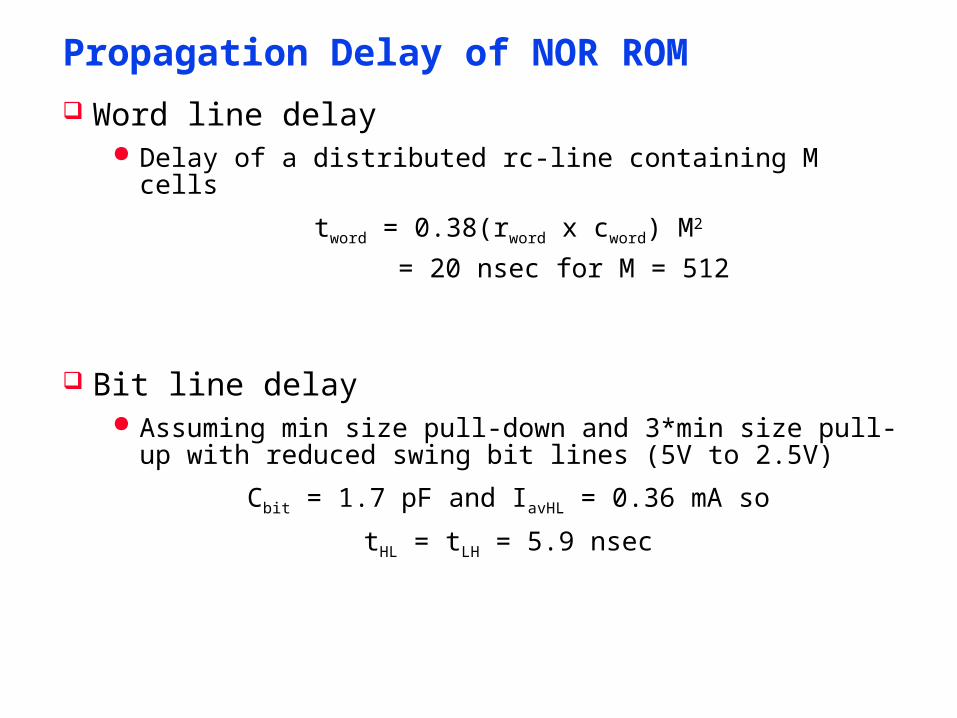
Propagation Delay of NOR ROM
Word line delay Delay of a distributed rc-line containing M cells
tword = 0.38(rword x cword) M2
= 20 nsec for M = 512
Bit line delay Assuming min size pull-down and 3*min size pull-up with
reduced swing bit lines (5V to 2.5V)
Cbit = 1.7 pF and IavHL = 0.36 mA so
tHL = tLH = 5.9 nsec
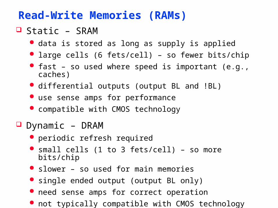
Read-Write Memories (RAMs) Static – SRAM
data is stored as long as supply is applied large cells (6 fets/cell) – so fewer bits/chip fast – so used where speed is important (e.g., caches) differential outputs (output BL and !BL) use sense amps for performance compatible with CMOS technology
Dynamic – DRAM periodic refresh required small cells (1 to 3 fets/cell) – so more bits/chip slower – so used for main memories single ended output (output BL only) need sense amps for correct operation not typically compatible with CMOS technology

Memory Timing Definitions
Read
Read Cycle
Read Access Read Access
Write
Write Cycle
Data
Write Setup
Data Valid
Write Hold

4x4 SRAM Memory
A0
Row
Dec
oder
!BLWL[0]
A1
A2
Column Decoder
sense amplifiers
write circuitry
BL
WL[1]
WL[2]
WL[3]
bit line precharge2 bit words
clocking and control
enable
read precharge
BL[i] BL[I+1]

2D Memory Configuration
Row
Dec
oder
Sense AmpsSense Amps

Decreasing Word Line Delay
Drive the word line from both sides
Use a metal bypass
Use silicides
polysilicon word line
metal word line
driverdriver
WL
polysilicon word line
metal bypass
WL

Decreasing Bit Line Delay (and Energy)
Reduce the bit line voltage swing need sense amp for each column to sense/restore signal
Isolate memory cells from the bit lines after sensing (to prevent the cells from changing the bit line voltage further) - pulsed word line
generation of word line pulses very critical- too short - sense amp operation may fail
- too long - power efficiency degraded (because bit line swing size depends on duration of the word line pulse)
use feedback signal from bit lines
Isolate sense amps from bit lines after sensing (to prevent bit lines from having large voltage swings) - bit line isolation
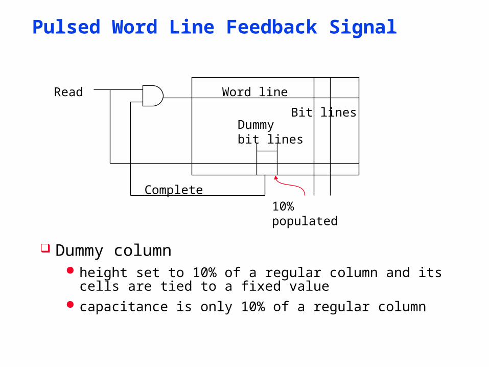
Pulsed Word Line Feedback Signal
Dummy column height set to 10% of a regular column and its cells are tied to
a fixed value capacitance is only 10% of a regular column
Read Word line
Bit lines
Complete
Dummybit lines
10%populated

Pulsed Word Line Timing
Dummy bit lines have reached full swing and trigger pulse shut off when regular bit lines reach 10% swing
Read
Complete
Word line
Bit line
Dummy bit line V = Vdd
V = 0.1Vdd

Bit Line Isolation
sense
Readsense amplifier
bit lines
isolate
sense amplifier outputs
V = 0.1Vdd
V = Vdd

6-transistor SRAM Cell
!BL BL
WL
M1
M2
M3
M4
M5M6Q
!Q