Research Article Fabrication of GaN-Based White Light...
6
Research Article Fabrication of GaN-Based White Light-Emitting Diodes on Yttrium Aluminum Garnet-Polydimethylsiloxane Flexible Substrates Lung-Chien Chen, Wen-Wei Lin, and Jun-Wei Chen Department of Electro-Optical Engineering, National University of Technology, 1, Sec. 3, Chung-Hsiao E. Road, Taipei 106, Taiwan Correspondence should be addressed to Lung-Chien Chen; [email protected] Received 15 April 2015; Accepted 31 August 2015 Academic Editor: Charles C. Sorrell Copyright © 2015 Lung-Chien Chen et al. is is an open access article distributed under the Creative Commons Attribution License, which permits unrestricted use, distribution, and reproduction in any medium, provided the original work is properly cited. is study concerns the characteristics of white GaN-based light-emitting diode (LED) on flexible substrates. e thin film GaN- based blue LEDs were directly transferred from sapphire onto the flexible polydimethylsiloxane (PDMS) substrates by laser liſt-off (LLO) process. e PDMS substrates were incorporated 10–40% cerium doped yttrium aluminum garnet phosphor, YAG:Ce 3+ , and formed the GaN-based white LEDs. e white LEDs prepared by the GaN-based LEDs on the YAG-PDMS substrates reveal one peak at 470nm corresponding to the emission of the GaN-based LED and a broadband included five weak peaks caused by YAG:Ce 3+ phosphors. 1. Introduction LEDs are regarded as the most important light source in next-generation solid-state lighting to advantages in energy efficiency, long life, high reliability, and multiple applica- tions [1, 2]. In recent years, due to the more benefits with flexible substrate, the fabrication of lighting sources on flexible substrates has been studied vigorously to develop, such as biomedical applications, deformable display, wearable devices, and flexible LEDs [3–6]. Several approaches have presented flexible light- emitting diodes (F-LEDs) by transferring microstructured GaAs/GaN to flexible substrates [7–10]. And the majority methods have produced flexible and highly efficient thin film GaN-based LEDs by laser liſt-off (LLO) technology [11–15]. In this study, we have prepared a polydimethylsilox- ane (PDMS) as a substrate which had the advantages of being flexible, low cost, good chemicophysical proper- ties and being good optically transparent. e fabrication of thin film GaN-based light-emitting diodes (GaN-based LEDs) was transferred from sapphire to flexible substrate by LLO method and produced the white light-emitting diode device. 2. Experimental 2.1. PDMS Substrate Production Process. PDMS solution was produced by mixing silicone resin agent (A agent) and curing agent (B agent) into liquid in weight ratio for 10 : 1. en, the yellow phosphor was incorporated into the PDMS solution and stirred uniformly. Aſterward, the PDMS incorporated YAG phosphor solution was placed in a vacuum chamber for 30 min so that bubbles disappeared. Polytetrafluoroethene (PTFE) is sprayed on the sapphire substrate to avoid PDMS sticking on sapphire. en, PDMS was uniformly coated on a sapphire substrate by spin coater (speed of 300 rpm and a coating time of 40sec). Subsequently, the PDMS substrate was treated at temperature of 120 ∘ C for 30 min to produce PDMS substrate. Finally, the cured PDMS substrate incorporated YAG phosphor (YAG-PDMS substrate) was removed from the sapphire substrate to produce white LED. 2.2. Preparation of White LED. e GaN-based light- emitting diode comprised a 3 m thick GaN:Si layer, five pairs of undoped InGaN/GaN multiple-quantum-wells (InGaN- GaN MQWs), and a 0.5 m thick layer of GaN:Mg sequen- tially on a (0001) oriented patterned sapphire substrate with a GaN buffer layer that was grown by metal-organic chemical Hindawi Publishing Corporation Advances in Materials Science and Engineering Volume 2015, Article ID 537163, 5 pages http://dx.doi.org/10.1155/2015/537163
Transcript of Research Article Fabrication of GaN-Based White Light...
Research ArticleFabrication of GaN-Based White Light-EmittingDiodes on Yttrium Aluminum Garnet-PolydimethylsiloxaneFlexible Substrates
Lung-Chien Chen, Wen-Wei Lin, and Jun-Wei Chen
Department of Electro-Optical Engineering, National University of Technology, 1, Sec. 3, Chung-Hsiao E. Road, Taipei 106, Taiwan
Correspondence should be addressed to Lung-Chien Chen; [email protected]
Received 15 April 2015; Accepted 31 August 2015
Academic Editor: Charles C. Sorrell
Copyright © 2015 Lung-Chien Chen et al. This is an open access article distributed under the Creative Commons AttributionLicense, which permits unrestricted use, distribution, and reproduction in any medium, provided the original work is properlycited.
This study concerns the characteristics of white GaN-based light-emitting diode (LED) on flexible substrates. The thin film GaN-based blue LEDs were directly transferred from sapphire onto the flexible polydimethylsiloxane (PDMS) substrates by laser lift-off(LLO) process. The PDMS substrates were incorporated 10–40% cerium doped yttrium aluminum garnet phosphor, YAG:Ce3+,and formed the GaN-based white LEDs. The white LEDs prepared by the GaN-based LEDs on the YAG-PDMS substrates revealone peak at 470 nm corresponding to the emission of the GaN-based LED and a broadband included five weak peaks caused byYAG:Ce3+ phosphors.
1. Introduction
LEDs are regarded as the most important light source innext-generation solid-state lighting to advantages in energyefficiency, long life, high reliability, and multiple applica-tions [1, 2]. In recent years, due to the more benefits withflexible substrate, the fabrication of lighting sources onflexible substrates has been studied vigorously to develop,such as biomedical applications, deformable display, wearabledevices, and flexible LEDs [3–6].
Several approaches have presented flexible light-emitting diodes (F-LEDs) by transferring microstructuredGaAs/GaN to flexible substrates [7–10]. And the majoritymethods have produced flexible and highly efficient thinfilm GaN-based LEDs by laser lift-off (LLO) technology[11–15].
In this study, we have prepared a polydimethylsilox-ane (PDMS) as a substrate which had the advantagesof being flexible, low cost, good chemicophysical proper-ties and being good optically transparent. The fabricationof thin film GaN-based light-emitting diodes (GaN-basedLEDs) was transferred from sapphire to flexible substrate byLLO method and produced the white light-emitting diodedevice.
2. Experimental
2.1. PDMS Substrate Production Process. PDMS solution wasproduced bymixing silicone resin agent (A agent) and curingagent (B agent) into liquid in weight ratio for 10 : 1. Then, theyellow phosphor was incorporated into the PDMS solutionand stirred uniformly. Afterward, the PDMS incorporatedYAG phosphor solution was placed in a vacuum chamberfor 30min so that bubbles disappeared. Polytetrafluoroethene(PTFE) is sprayed on the sapphire substrate to avoid PDMSsticking on sapphire. Then, PDMS was uniformly coatedon a sapphire substrate by spin coater (speed of 300 rpmand a coating time of 40 sec). Subsequently, the PDMSsubstrate was treated at temperature of 120∘C for 30min toproduce PDMS substrate. Finally, the cured PDMS substrateincorporated YAG phosphor (YAG-PDMS substrate) wasremoved from the sapphire substrate to produce white LED.
2.2. Preparation of White LED. The GaN-based light-emitting diode comprised a 3𝜇mthickGaN:Si layer, five pairsof undoped InGaN/GaN multiple-quantum-wells (InGaN-GaN MQWs), and a 0.5 𝜇m thick layer of GaN:Mg sequen-tially on a (0001) oriented patterned sapphire substrate witha GaN buffer layer that was grown bymetal-organic chemical
Hindawi Publishing CorporationAdvances in Materials Science and EngineeringVolume 2015, Article ID 537163, 5 pageshttp://dx.doi.org/10.1155/2015/537163
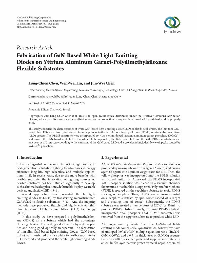
2 Advances in Materials Science and Engineering
Hexagonal pyramid hillocks
(10-1-1)
(a)
ITO
N-type GaN
InGaN/GaN MQWsP-type GaN
Ni/Au
YAG-PDMS
(b)
Figure 1: (a) Surface of the n-GaN epitaxial layer after KOH solution etching and (b) GaN-based LED after LLO process was mounted onflexible YAG-PDMS substrate.
GaN-based LED on sapphire substrateGaN-based LED on flexible YAG-PDMS
−0.01
0.00
0.01
0.02
0.03
0.04
0.05
0.06
0.07
0.08
Curr
ent (
A)
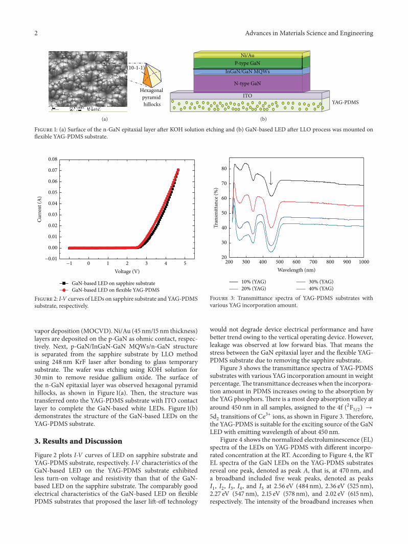
0 1 2 3 4 5−1
Voltage (V)
Figure 2: I-V curves of LEDs on sapphire substrate and YAG-PDMSsubstrate, respectively.
vapor deposition (MOCVD). Ni/Au (45 nm/15 nm thickness)layers are deposited on the p-GaN as ohmic contact, respec-tively. Next, p-GaN/InGaN-GaN MQWs/n-GaN structureis separated from the sapphire substrate by LLO methodusing 248 nm KrF laser after bonding to glass temporarysubstrate. The wafer was etching using KOH solution for30min to remove residue gallium oxide. The surface ofthe n-GaN epitaxial layer was observed hexagonal pyramidhillocks, as shown in Figure 1(a). Then, the structure wastransferred onto the YAG-PDMS substrate with ITO contactlayer to complete the GaN-based white LEDs. Figure 1(b)demonstrates the structure of the GaN-based LEDs on theYAG-PDMS substrate.
3. Results and Discussion
Figure 2 plots I-V curves of LED on sapphire substrate andYAG-PDMS substrate, respectively. I-V characteristics of theGaN-based LED on the YAG-PDMS substrate exhibitedless turn-on voltage and resistivity than that of the GaN-based LED on the sapphire substrate. The comparably goodelectrical characteristics of the GaN-based LED on flexiblePDMS substrates that proposed the laser lift-off technology
300 400 500 600 700 800 900 1000200Wavelength (nm)
20
30
40
50
60
70
80
Tran
smitt
ance
(%)
10% (YAG)20% (YAG)
30% (YAG)40% (YAG)
Figure 3: Transmittance spectra of YAG-PDMS substrates withvarious YAG incorporation amount.
would not degrade device electrical performance and havebetter trend owing to the vertical operating device. However,leakage was observed at low forward bias. That means thestress between the GaN epitaxial layer and the flexible YAG-PDMS substrate due to removing the sapphire substrate.
Figure 3 shows the transmittance spectra of YAG-PDMSsubstrates with various YAG incorporation amount in weightpercentage.The transmittance decreases when the incorpora-tion amount in PDMS increases owing to the absorption bythe YAG phosphors.There is a most deep absorption valley ataround 450 nm in all samples, assigned to the 4f (2F
5/2) →
5d2transitions of Ce3+ ions, as shown in Figure 3. Therefore,
the YAG-PDMS is suitable for the exciting source of the GaNLED with emitting wavelength of about 450 nm.
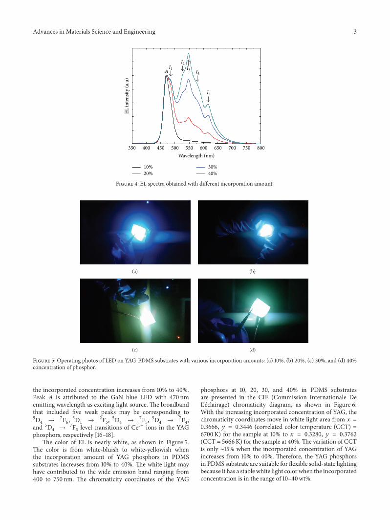
Figure 4 shows the normalized electroluminescence (EL)spectra of the LEDs on YAG-PDMS with different incorpo-rated concentration at the RT. According to Figure 4, the RTEL spectra of the GaN LEDs on the YAG-PDMS substratesreveal one peak, denoted as peak 𝐴, that is, at 470 nm, anda broadband included five weak peaks, denoted as peaks𝐼1, 𝐼2, 𝐼3, 𝐼4, and 𝐼
5at 2.56 eV (484 nm), 2.36 eV (525 nm),
2.27 eV (547 nm), 2.15 eV (578 nm), and 2.02 eV (615 nm),respectively. The intensity of the broadband increases when
Advances in Materials Science and Engineering 3
EL in
tens
ity (a
.u)
A
400 450 500 550 600 650 700 750 800350Wavelength (nm)
I1
I2I3 I4
I5
10%20%
30%40%
Figure 4: EL spectra obtained with different incorporation amount.
(a) (b)
(c) (d)
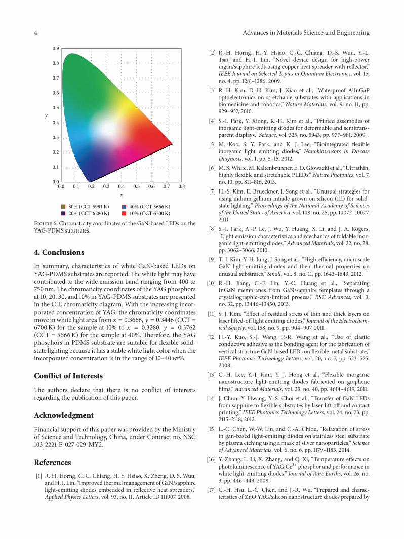
Figure 5: Operating photos of LED on YAG-PDMS substrates with various incorporation amounts: (a) 10%, (b) 20%, (c) 30%, and (d) 40%concentration of phosphor.
the incorporated concentration increases from 10% to 40%.Peak 𝐴 is attributed to the GaN blue LED with 470 nmemitting wavelength as exciting light source. The broadbandthat included five weak peaks may be corresponding to5D4→7F6, 5D1→2F5, 5D4→7F5, 5D4→7F4,
and 5D4→7F3level transitions of Ce3+ ions in the YAG
phosphors, respectively [16–18].The color of EL is nearly white, as shown in Figure 5.
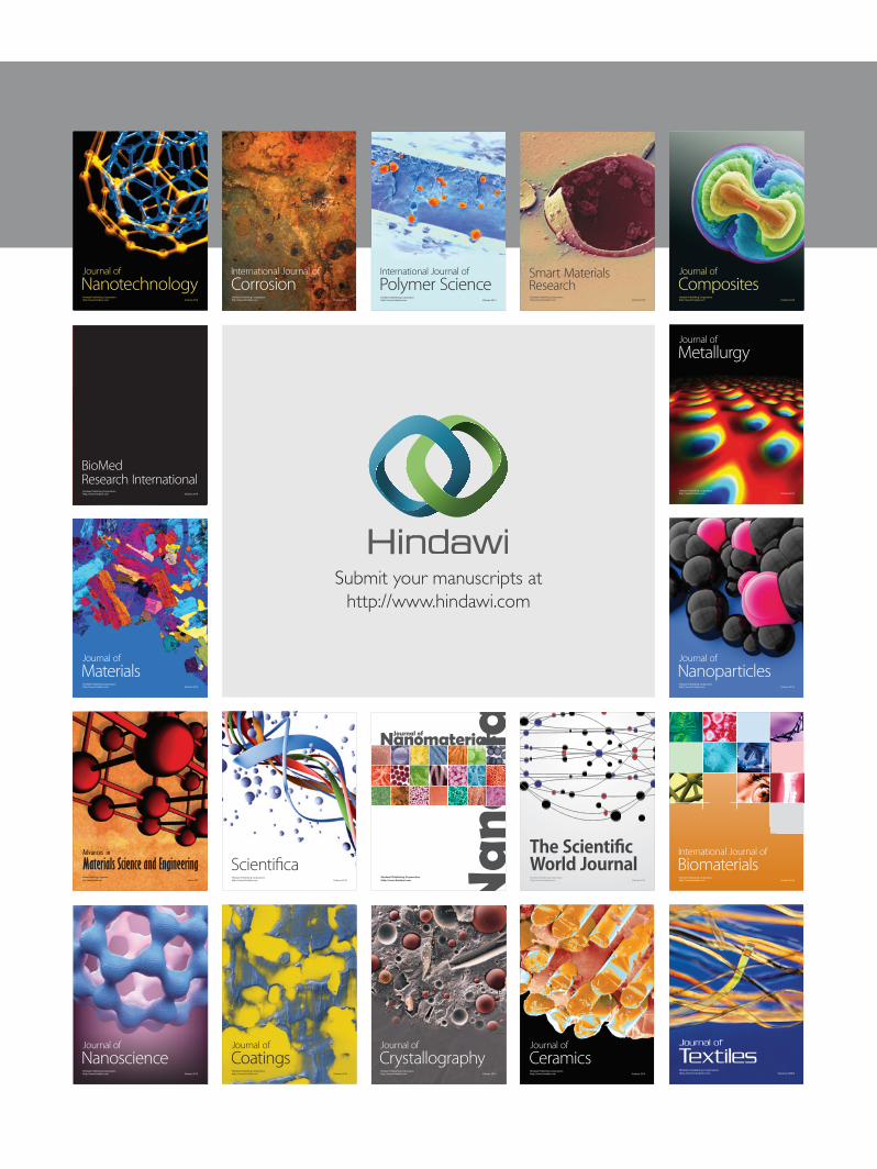
The color is from white-bluish to white-yellowish whenthe incorporation amount of YAG phosphors in PDMSsubstrates increases from 10% to 40%. The white light mayhave contributed to the wide emission band ranging from400 to 750 nm. The chromaticity coordinates of the YAG
phosphors at 10, 20, 30, and 40% in PDMS substratesare presented in the CIE (Commission Internationale DeL’eclairage) chromaticity diagram, as shown in Figure 6.With the increasing incorporated concentration of YAG, thechromaticity coordinates move in white light area from 𝑥 =0.3666, 𝑦 = 0.3446 (correlated color temperature (CCT) =6700K) for the sample at 10% to 𝑥 = 0.3280, 𝑦 = 0.3762(CCT = 5666K) for the sample at 40%.The variation of CCTis only ∼15% when the incorporated concentration of YAGincreases from 10% to 40%. Therefore, the YAG phosphorsin PDMS substrate are suitable for flexible solid-state lightingbecause it has a stable white light color when the incorporatedconcentration is in the range of 10–40wt%.
4 Advances in Materials Science and Engineering
30% (CCT 5991K)20% (CCT 6280K)
40% (CCT 5666K)10% (CCT 6700K)
0.9
0.8
0.7
0.6
0.5
0.4
0.3
0.2
0.1
0.00.0 0.1 0.2 0.3 0.4 0.5 0.6 0.7 0.8
x
y
Figure 6: Chromaticity coordinates of the GaN-based LEDs on theYAG-PDMS substrates.
4. Conclusions
In summary, characteristics of white GaN-based LEDs onYAG-PDMS substrates are reported.Thewhite lightmay havecontributed to the wide emission band ranging from 400 to750 nm.The chromaticity coordinates of the YAG phosphorsat 10, 20, 30, and 10% in YAG-PDMS substrates are presentedin the CIE chromaticity diagram. With the increasing incor-porated concentration of YAG, the chromaticity coordinatesmove in white light area from 𝑥 = 0.3666, 𝑦 = 0.3446 (CCT =6700K) for the sample at 10% to 𝑥 = 0.3280, 𝑦 = 0.3762(CCT = 5666K) for the sample at 40%. Therefore, the YAGphosphors in PDMS substrate are suitable for flexible solid-state lighting because it has a stable white light color when theincorporated concentration is in the range of 10–40wt%.
Conflict of Interests
The authors declare that there is no conflict of interestsregarding the publication of this paper.
Acknowledgment
Financial support of this paper was provided by the Ministryof Science and Technology, China, under Contract no. NSC103-2221-E-027-029-MY2.
References
[1] R. H. Horng, C. C. Chiang, H. Y. Hsiao, X. Zheng, D. S. Wuu,andH. I. Lin, “Improved thermalmanagement ofGaN/sapphirelight-emitting diodes embedded in reflective heat spreaders,”Applied Physics Letters, vol. 93, no. 11, Article ID 111907, 2008.
[2] R.-H. Horng, H.-Y. Hsiao, C.-C. Chiang, D.-S. Wuu, Y.-L.Tsai, and H.-I. Lin, “Novel device design for high-poweringan/sapphire leds using copper heat spreader with reflector,”IEEE Journal on Selected Topics in Quantum Electronics, vol. 15,no. 4, pp. 1281–1286, 2009.
[3] R.-H. Kim, D.-H. Kim, J. Xiao et al., “Waterproof AlInGaPoptoelectronics on stretchable substrates with applications inbiomedicine and robotics,” Nature Materials, vol. 9, no. 11, pp.929–937, 2010.
[4] S.-I. Park, Y. Xiong, R.-H. Kim et al., “Printed assemblies ofinorganic light-emitting diodes for deformable and semitrans-parent displays,” Science, vol. 325, no. 5943, pp. 977–981, 2009.
[5] M. Koo, S. Y. Park, and K. J. Lee, “Biointegrated flexibleinorganic light emitting diodes,” Nanobiosensors in DiseaseDiagnosis, vol. 1, pp. 5–15, 2012.
[6] M. S.White,M.Kaltenbrunner, E.D.Głowacki et al., “Ultrathin,highly flexible and stretchable PLEDs,” Nature Photonics, vol. 7,no. 10, pp. 811–816, 2013.
[7] H.-S. Kim, E. Brueckner, J. Song et al., “Unusual strategies forusing indium gallium nitride grown on silicon (111) for solid-state lighting,” Proceedings of the National Academy of Sciencesof the United States of America, vol. 108, no. 25, pp. 10072–10077,2011.
[8] S.-I. Park, A.-P. Le, J. Wu, Y. Huang, X. Li, and J. A. Rogers,“Light emission characteristics and mechanics of foldable inor-ganic light-emitting diodes,”AdvancedMaterials, vol. 22, no. 28,pp. 3062–3066, 2010.
[9] T.-I. Kim, Y. H. Jung, J. Song et al., “High-efficiency, microscaleGaN light-emitting diodes and their thermal properties onunusual substrates,” Small, vol. 8, no. 11, pp. 1643–1649, 2012.
[10] R.-H. Jiang, C.-F. Lin, Y.-C. Huang et al., “SeparatingInGaN membranes from GaN/sapphire templates through acrystallographic-etch-limited process,” RSC Advances, vol. 3,no. 32, pp. 13446–13450, 2013.
[11] S. J. Kim, “Effect of residual stress of thin and thick layers onlaser lifted-off light emitting diodes,” Journal of the Electrochem-ical Society, vol. 158, no. 9, pp. 904–907, 2011.
[12] H.-Y. Kuo, S.-J. Wang, P.-R. Wang et al., “Use of elasticconductive adhesive as the bonding agent for the fabrication ofvertical structure GaN-based LEDs on flexible metal substrate,”IEEE Photonics Technology Letters, vol. 20, no. 7, pp. 523–525,2008.
[13] C.-H. Lee, Y.-J. Kim, Y. J. Hong et al., “Flexible inorganicnanostructure light-emitting diodes fabricated on graphenefilms,” Advanced Materials, vol. 23, no. 40, pp. 4614–4619, 2011.
[14] J. Chun, Y. Hwang, Y.-S. Choi et al., “Transfer of GaN LEDsfrom sapphire to flexible substrates by laser lift-off and contactprinting,” IEEE Photonics Technology Letters, vol. 24, no. 23, pp.2115–2118, 2012.
[15] L.-C. Chen, W.-W. Lin, and C.-A. Chiou, “Relaxation of stressin gan-based light-emitting diodes on stainless steel substrateby plasma etching using a mask of silver nanoparticles,” Scienceof Advanced Materials, vol. 6, no. 6, pp. 1179–1183, 2014.
[16] Y. Zhang, L. Li, X. Zhang, and Q. Xi, “Temperature effects onphotoluminescence of YAG:Ce3+ phosphor and performance inwhite light-emitting diodes,” Journal of Rare Earths, vol. 26, no.3, pp. 446–449, 2008.
[17] C.-H. Hsu, L.-C. Chen, and J.-R. Wu, “Prepared and charac-teristics of ZnO:YAG/silicon nanostructure diodes prepared by

Advances in Materials Science and Engineering 5
ultrasonic spraying,” International Journal of Photoenergy, vol.2014, Article ID 128235, 6 pages, 2014.
[18] R. Kasuya, A. Kawano, T. Isobe, H. Kuma, and J. Katano, “Char-acteristic optical properties of transparent color conversionfilm prepared from YAG:Ce3+ nanoparticles,” Applied PhysicsLetters, vol. 91, no. 11, Article ID 111916, 2007.
Submit your manuscripts athttp://www.hindawi.com
ScientificaHindawi Publishing Corporationhttp://www.hindawi.com Volume 2014
CorrosionInternational Journal of
Hindawi Publishing Corporationhttp://www.hindawi.com Volume 2014
Polymer ScienceInternational Journal of
Hindawi Publishing Corporationhttp://www.hindawi.com Volume 2014
Hindawi Publishing Corporationhttp://www.hindawi.com Volume 2014
CeramicsJournal of
Hindawi Publishing Corporationhttp://www.hindawi.com Volume 2014
CompositesJournal of
NanoparticlesJournal of
Hindawi Publishing Corporationhttp://www.hindawi.com Volume 2014
Hindawi Publishing Corporationhttp://www.hindawi.com Volume 2014
International Journal of
Biomaterials
Hindawi Publishing Corporationhttp://www.hindawi.com Volume 2014
NanoscienceJournal of
TextilesHindawi Publishing Corporation http://www.hindawi.com Volume 2014
Journal of
NanotechnologyHindawi Publishing Corporationhttp://www.hindawi.com Volume 2014
Journal of
CrystallographyJournal of
Hindawi Publishing Corporationhttp://www.hindawi.com Volume 2014
The Scientific World JournalHindawi Publishing Corporation http://www.hindawi.com Volume 2014
Hindawi Publishing Corporationhttp://www.hindawi.com Volume 2014
CoatingsJournal of
Advances in
Materials Science and EngineeringHindawi Publishing Corporationhttp://www.hindawi.com Volume 2014
Smart Materials Research
Hindawi Publishing Corporationhttp://www.hindawi.com Volume 2014
Hindawi Publishing Corporationhttp://www.hindawi.com Volume 2014
MetallurgyJournal of
Hindawi Publishing Corporationhttp://www.hindawi.com Volume 2014
BioMed Research International
MaterialsJournal of
Hindawi Publishing Corporationhttp://www.hindawi.com Volume 2014
Nano
materials
Hindawi Publishing Corporationhttp://www.hindawi.com Volume 2014
Journal ofNanomaterials