Registers - جامعة نزوى · Shift Registers -A register capable of shifting the binary...
18
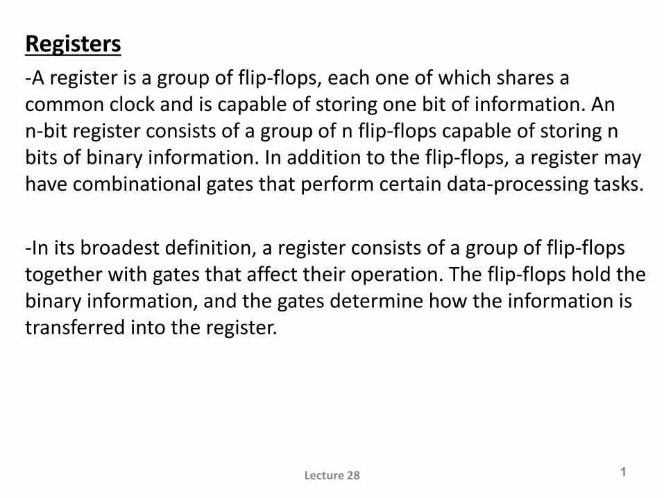
Registers -A register is a group of flip‐flops, each one of which shares a common clock and is capable of storing one bit of information. An n‐bit register consists of a group of n flip‐flops capable of storing n bits of binary information. In addition to the flip‐flops, a register may have combinational gates that perform certain data‐processing tasks. -In its broadest definition, a register consists of a group of flip‐flops together with gates that affect their operation. The flip‐flops hold the binary information, and the gates determine how the information is transferred into the register. Lecture 28 1
Transcript of Registers - جامعة نزوى · Shift Registers -A register capable of shifting the binary...
Registers
-A register is a group of flip‐flops, each one of which shares a common clock and is capable of storing one bit of information. An n‐bit register consists of a group of n flip‐flops capable of storing n bits of binary information. In addition to the flip‐flops, a register may have combinational gates that perform certain data‐processing tasks.
-In its broadest definition, a register consists of a group of flip‐flops together with gates that affect their operation. The flip‐flops hold the binary information, and the gates determine how the information is transferred into the register.
Lecture 28 1
Lecture 28 2
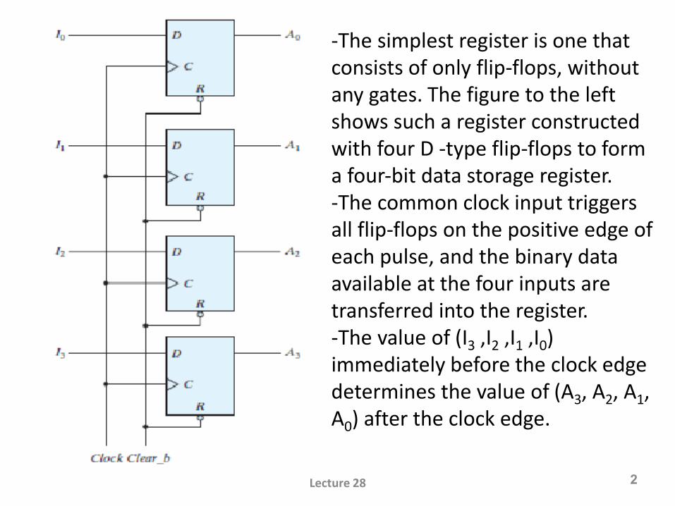
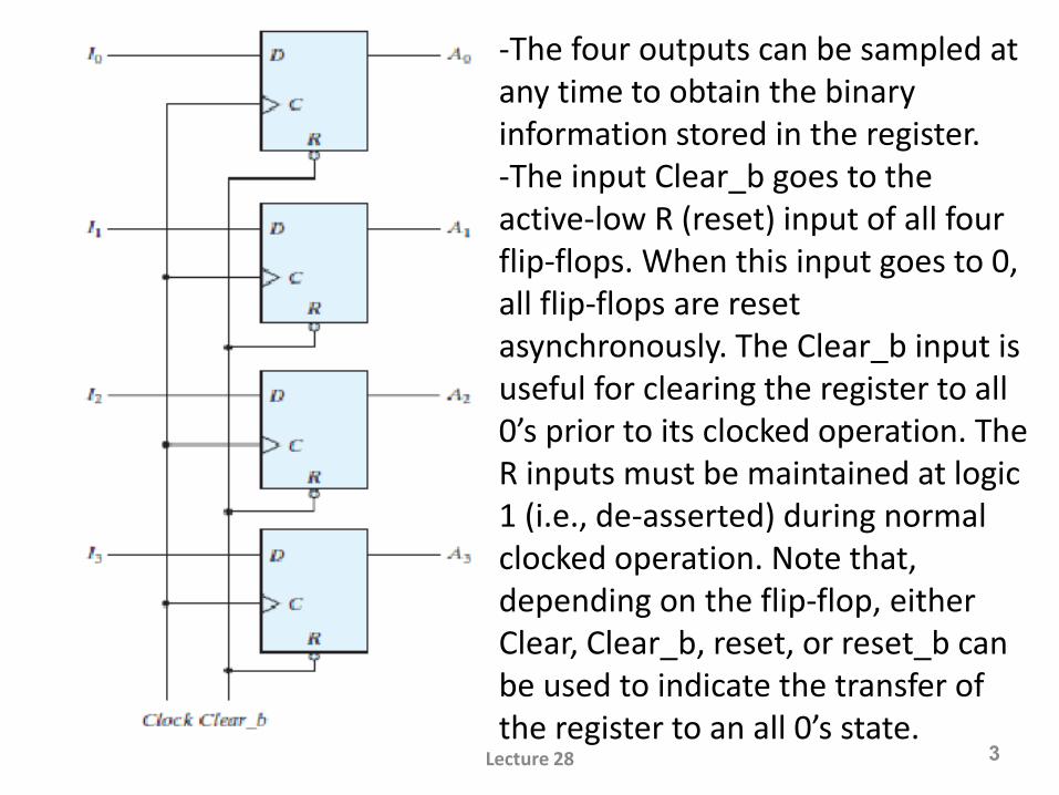
-The simplest register is one that consists of only flip‐flops, without any gates. The figure to the left shows such a register constructed with four D ‐type flip‐flops to form a four‐bit data storage register. -The common clock input triggers all flip‐flops on the positive edge of each pulse, and the binary data available at the four inputs are transferred into the register. -The value of (I3 ,I2 ,I1 ,I0) immediately before the clock edge determines the value of (A3, A2, A1, A0) after the clock edge.
Lecture 28 3
-The four outputs can be sampled at any time to obtain the binary information stored in the register. -The input Clear_b goes to the active‐low R (reset) input of all four flip‐flops. When this input goes to 0, all flip‐flops are reset asynchronously. The Clear_b input is useful for clearing the register to all 0’s prior to its clocked operation. The R inputs must be maintained at logic 1 (i.e., de-asserted) during normal clocked operation. Note that, depending on the flip‐flop, either Clear, Clear_b, reset, or reset_b can be used to indicate the transfer of the register to an all 0’s state.
Lecture 28 4
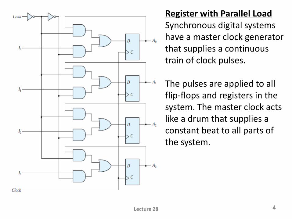
Register with Parallel Load Synchronous digital systems have a master clock generator that supplies a continuous train of clock pulses. The pulses are applied to all flip‐flops and registers in the system. The master clock acts like a drum that supplies a constant beat to all parts of the system.
Lecture 28 5
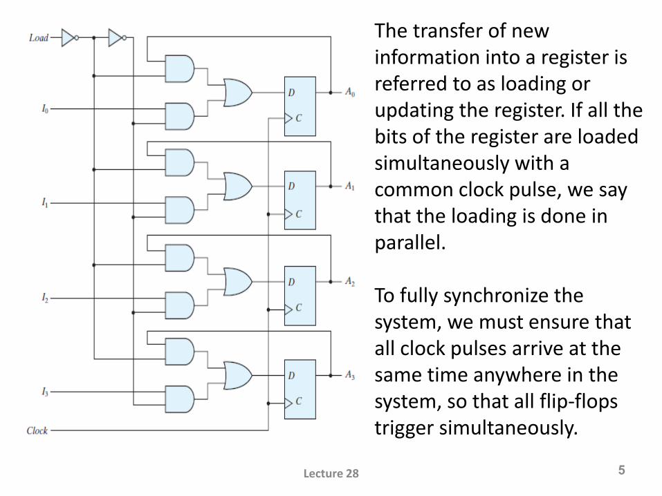
The transfer of new information into a register is referred to as loading or updating the register. If all the bits of the register are loaded simultaneously with a common clock pulse, we say that the loading is done in parallel. To fully synchronize the system, we must ensure that all clock pulses arrive at the same time anywhere in the system, so that all flip‐flops trigger simultaneously.
Lecture 28 6
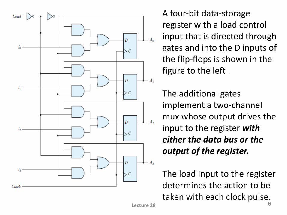
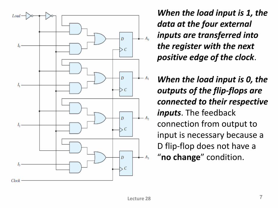
A four‐bit data‐storage register with a load control input that is directed through gates and into the D inputs of the flip‐flops is shown in the figure to the left . The additional gates implement a two‐channel mux whose output drives the input to the register with either the data bus or the output of the register. The load input to the register determines the action to be taken with each clock pulse.
Lecture 28 7
When the load input is 1, the data at the four external inputs are transferred into the register with the next positive edge of the clock. When the load input is 0, the outputs of the flip‐flops are connected to their respective inputs. The feedback connection from output to input is necessary because a D flip‐flop does not have a “no change” condition.
Lecture 28 8
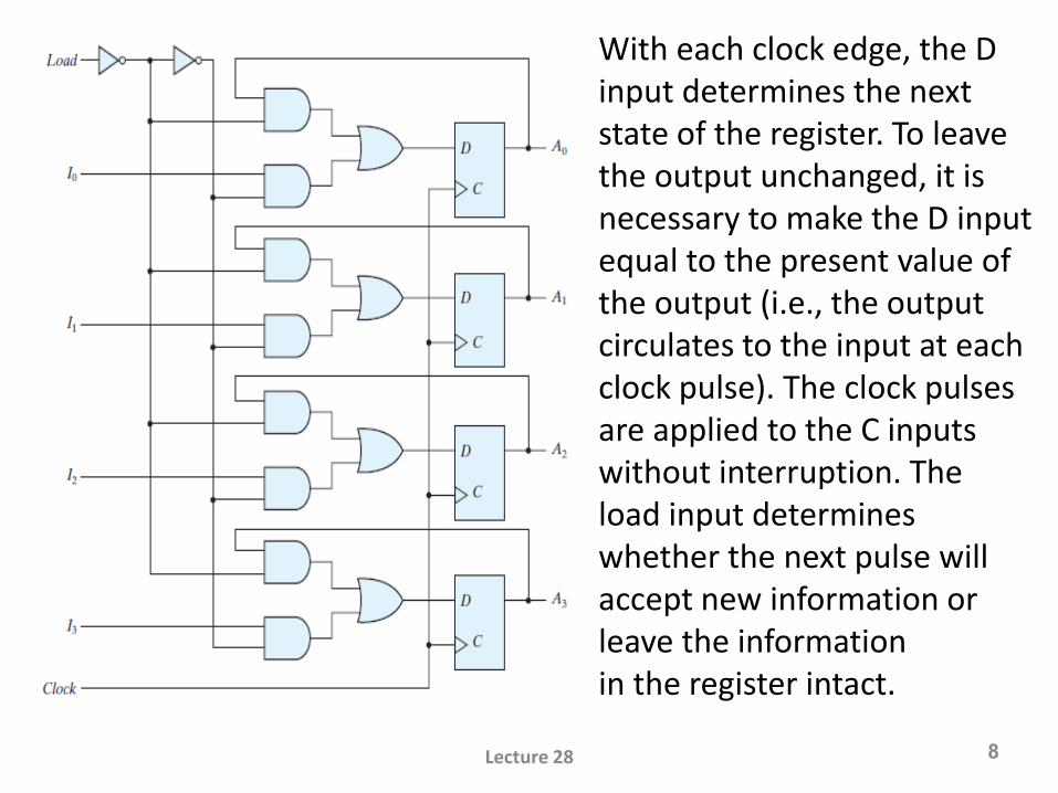
With each clock edge, the D input determines the next state of the register. To leave the output unchanged, it is necessary to make the D input equal to the present value of the output (i.e., the output circulates to the input at each clock pulse). The clock pulses are applied to the C inputs without interruption. The load input determines whether the next pulse will accept new information or leave the information in the register intact.
Lecture 28 9
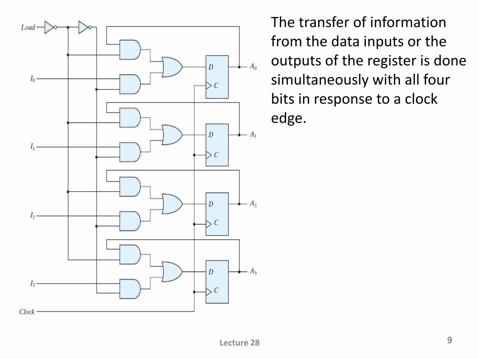
The transfer of information from the data inputs or the outputs of the register is done simultaneously with all four bits in response to a clock edge.
Shift Registers
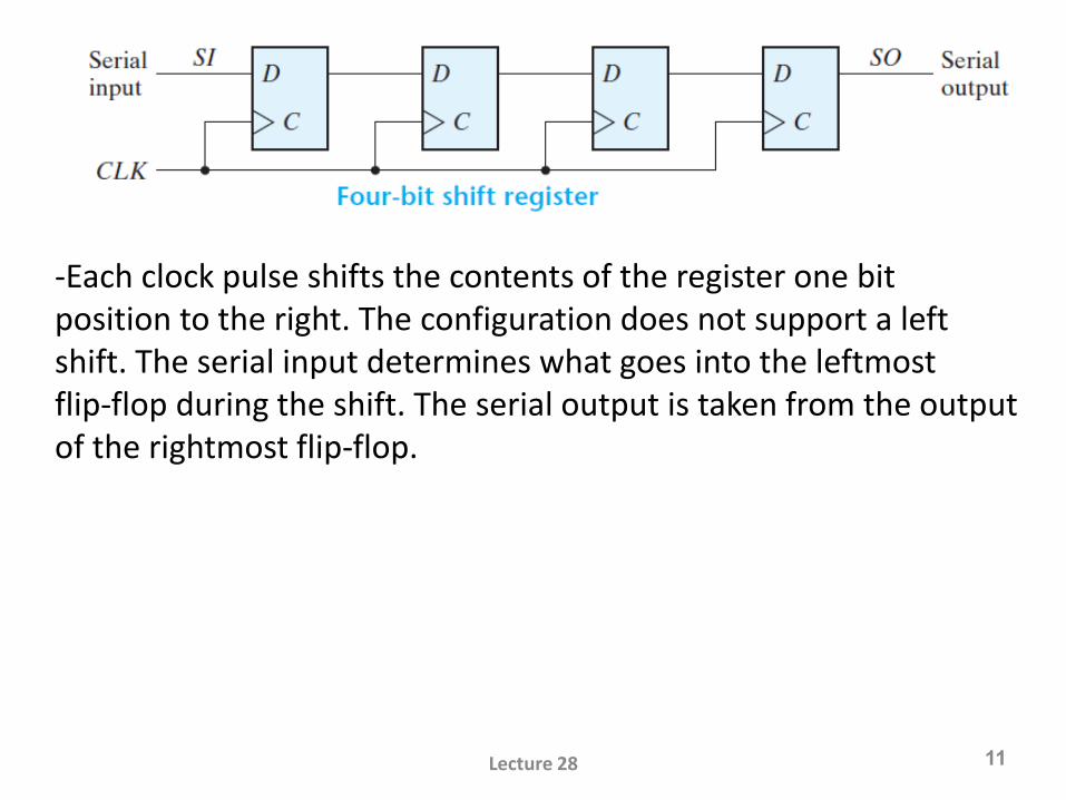
-A register capable of shifting the binary information held in each cell to its neighboring cell, in a selected direction, is called a shift register. The logical configuration of a shift register consists of a chain of flip‐flops in cascade, with the output of one flip‐flop connected to the input of the next flip‐flop. All flip‐flops receive common clock pulses, which activate the shift of data from one stage to the next.
-The simplest possible shift register is one that uses only flip‐flops, as shown in the next slide. The output of a given flip‐flop is connected to the D input of the flip‐flop at its right. This shift register is unidirectional (left‐to‐right).
Lecture 28 10
Lecture 28 11
-Each clock pulse shifts the contents of the register one bit position to the right. The configuration does not support a left shift. The serial input determines what goes into the leftmost flip‐flop during the shift. The serial output is taken from the output of the rightmost flip‐flop.
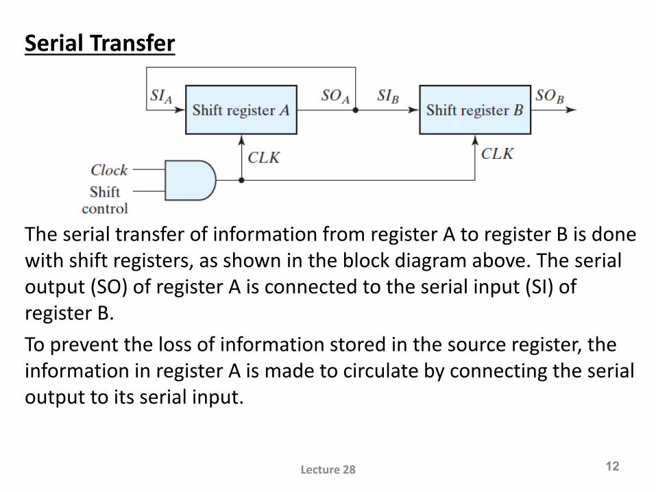
Serial Transfer
The serial transfer of information from register A to register B is done with shift registers, as shown in the block diagram above. The serial output (SO) of register A is connected to the serial input (SI) of register B.
To prevent the loss of information stored in the source register, the information in register A is made to circulate by connecting the serial output to its serial input.
Lecture 28 12
Lecture 28 13
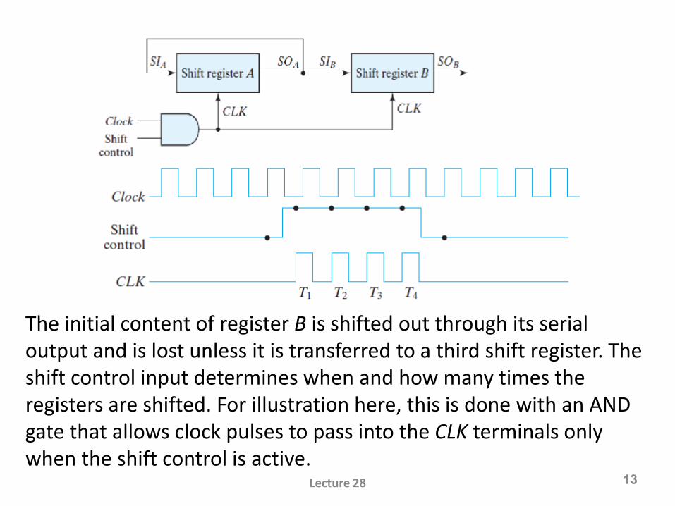
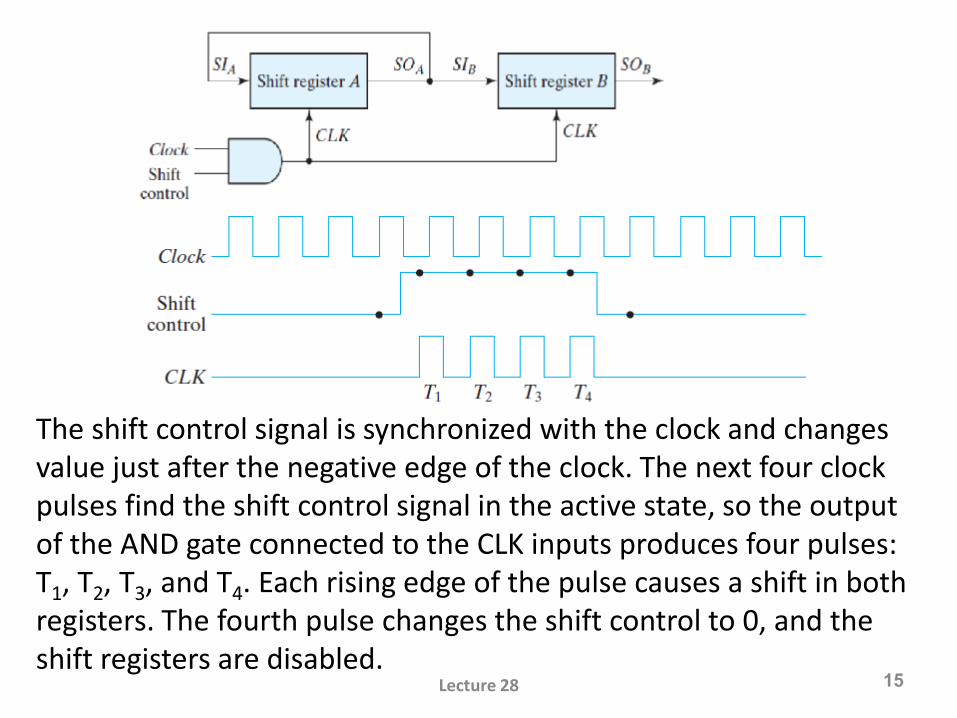
The initial content of register B is shifted out through its serial output and is lost unless it is transferred to a third shift register. The shift control input determines when and how many times the registers are shifted. For illustration here, this is done with an AND gate that allows clock pulses to pass into the CLK terminals only when the shift control is active.
Lecture 28 14
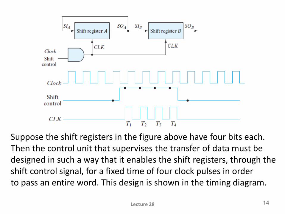
Suppose the shift registers in the figure above have four bits each. Then the control unit that supervises the transfer of data must be designed in such a way that it enables the shift registers, through the shift control signal, for a fixed time of four clock pulses in order to pass an entire word. This design is shown in the timing diagram.
Lecture 28 15
The shift control signal is synchronized with the clock and changes value just after the negative edge of the clock. The next four clock pulses find the shift control signal in the active state, so the output of the AND gate connected to the CLK inputs produces four pulses: T1, T2, T3, and T4. Each rising edge of the pulse causes a shift in both registers. The fourth pulse changes the shift control to 0, and the shift registers are disabled.
Lecture 28 16
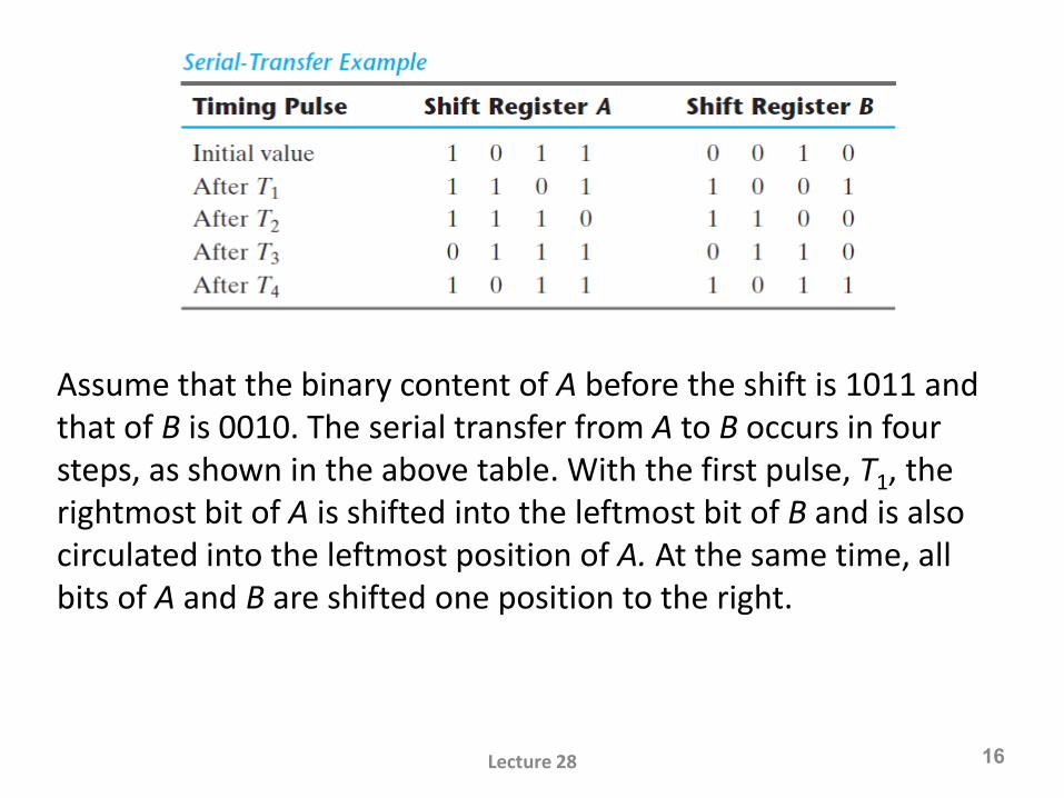
Assume that the binary content of A before the shift is 1011 and that of B is 0010. The serial transfer from A to B occurs in four steps, as shown in the above table. With the first pulse, T1, the rightmost bit of A is shifted into the leftmost bit of B and is also circulated into the leftmost position of A. At the same time, all bits of A and B are shifted one position to the right.
Lecture 28 17
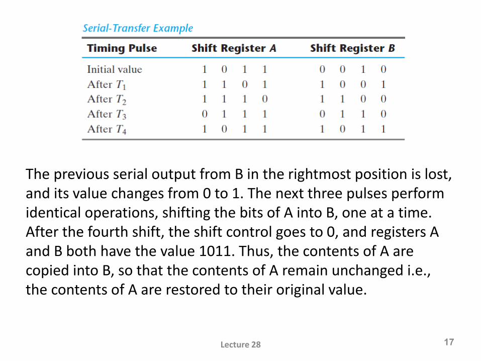
The previous serial output from B in the rightmost position is lost, and its value changes from 0 to 1. The next three pulses perform identical operations, shifting the bits of A into B, one at a time. After the fourth shift, the shift control goes to 0, and registers A and B both have the value 1011. Thus, the contents of A are copied into B, so that the contents of A remain unchanged i.e., the contents of A are restored to their original value.
The difference between the serial and the parallel mode of operation should be apparent from this example. In the parallel mode, information is available from all bits of a register and all bits can be transferred simultaneously during one clock pulse.
In the serial mode, the registers have a single serial input and a single serial output. The information is transferred one bit at a time while the registers are shifted in the same direction.
Lecture 28 18