Antibacterial and antibiofilm properties of yttrium fluoride nanoparticles
Reducing graphene device variability with yttrium sacrificial layers
Ning C. Wang,1 Enrique A. Carrion,2 Maryann C. Tung,1 and Eric Pop1,3,a)
1Department of Electrical Engineering, Stanford University, Stanford, California 94305, USA2Department of Electrical and Computer Engineering and Micro and Nanotechnology Lab,University of Illinois at Urbana-Champaign, Urbana, Illinois 61801, USA3Department of Materials Science and Engineering, Stanford University, Stanford, California 94305, USA
(Received 8 February 2017; accepted 12 May 2017; published online 31 May 2017)
Graphene technology has made great strides since the material was isolated more than a decade
ago. However, despite improvements in growth quality and numerous “hero” devices, challenges
of uniformity remain, restricting the large-scale development of graphene-based technologies.
Here, we investigate and reduce the variability of graphene transistors by studying the effects of
contact metals (with and without a Ti layer), resist, and yttrium (Y) sacrificial layers during the
fabrication of hundreds of devices. We find that with optical photolithography, residual resist and
process contamination are unavoidable, ultimately limiting the device performance and yield.
However, using Y sacrificial layers to isolate the graphene from processing conditions improves
the yield (from 73% to 97%), the average device performance (three-fold increase of mobility
and 58% lower contact resistance), and the device-to-device variability (standard deviation of
Dirac voltage reduced by 20%). In contrast to other sacrificial layer techniques, the removal of the
Y sacrificial layer with dilute HCl does not harm surrounding materials, simplifying large-scale
graphene fabrication. Published by AIP Publishing. [http://dx.doi.org/10.1063/1.4984090]
Since the first experimental demonstration of monolayer
graphene in 2004,1 academic and industrial research labs
have extensively explored applications that leverage the
unique electrical, mechanical, and thermal properties of
this material. To date, these efforts have yielded promising
results for chemical sensors,2 transparent and flexible elec-
tronics,3 and analog circuits.4 Rapid advances in large-scale
production of graphene via chemical vapor deposition (CVD)
have also accelerated the development and mass-production
of graphene towards practical applications.5
While unique physical properties motivate research in
graphene electronics, the device yield and spatial variability
will ultimately dictate the industrial impact. To this end,
many works have focused on improving the quality and cost
of large-scale CVD graphene growth and transfers,6,7 but
fewer have attempted to quantify and reduce the detrimental
effects of subsequent device fabrication, which may lead to
inconsistencies in reported results. Optical photolithogra-
phy—critical for large-scale fabrication—is particularly prob-
lematic as photoresist (PR) residues on the graphene surface
negatively impact the device performance.8 Additionally,
post-fabrication residue removal methods, such as non-
selective physical etches with CO2,9 are difficult to reproduce
in a controlled manner and may damage graphene by induc-
ing tears and wrinkles.
In contrast to post-fabrication cleaning methods, modi-
fying and optimizing a process flow to protect graphene
from its interaction with PR is a more suitable approach. The
semiconductor industry has employed native SiO2 as a sacri-
ficial protection layer for Si during integrated circuit fabrica-
tion. However, since graphene has no equivalent native
oxide, thin aluminum (Al) and titanium (Ti) layers have
been introduced as sacrificial layers.10–12 Subsequent
removal is nontrivial and can affect the graphene and sur-
rounding materials (i.e., substrates, insulators, and PR) dur-
ing fabrication. For example, Al removal via the AZ422
developer12 lengthens resist development times, potentially
leading to the overdevelopment and reduced yield of small
features. For Ti removal,10 hydrofluoric (HF) acid is utilized.
However, HF can etch underneath the graphene and delami-
nate devices from the substrate, lowering the device yield on
oxide substrates such as SiO2.
In this work, we introduce the use of yttrium (Y) sacrifi-
cial layers to protect graphene. Y is an ideal material for this
purpose, as it (1) readily forms a sub-stoichiometric oxide
that does not degrade electrical transport13 and (2) is etched
in dilute hydrochloric acid (HCl), which is safe for both SiO2
and PR. The latter point greatly simplifies fabrication, result-
ing in higher device yield, and differentiates the Y-sacrificial
method from existing alternatives. We fabricate and measure
hundreds of devices, employing transport models and materials
analysis to physically quantify the cause of fabrication-induced
degradation. We then introduce the use of Y-sacrificial layers
to alleviate degradation, reduce variability, increase perfor-
mance (three-fold intrinsic mobility improvement and 58%
decrease in contact resistance), and improve our device yield
up to 97%.
Figure 1 outlines the process flow used, including the
implementation of the Y-sacrificial layer. Complete fabrica-
tion details are given in the supplementary material, and
we outline here the material characterization relevant to
Y-sacrificial layer processing. Monolayer graphene is first
grown on Cu foils by chemical vapor deposition at 1000 C,
using isopropyl alcohol (IPA) or a CH4 carbon source (addi-
tional details are given in the supplementary material). The
graphene is then transferred onto 90 nm SiO2 on pþ Sia)Author to whom correspondence should be addressed: [email protected]
0003-6951/2017/110(22)/223106/5/$30.00 Published by AIP Publishing.110, 223106-1
APPLIED PHYSICS LETTERS 110, 223106 (2017)

(<0.005 X cm) substrates with a poly(methyl methacrylate)
(PMMA) support scaffold14 [Fig. 1(a)], applying a modified
RCA cleaning process7 to minimize wrinkles and impurities
(i.e., Fe, Cl, and Cu). Immediately after transfer and prior
to device fabrication, the samples are coated with 5 nm
of Y via electron-beam evaporation at a base pressure of
107 Torr to isolate and protect the underlying graphene
[Fig. 1(b)]. The Y-coated samples are not metallic, indicating
that the Y film is oxidized upon exposure to air after
deposition.
To characterize the effects of process conditions on
device quality, we fabricate back-gated graphene field-effect
transistors (GFETs) by ultraviolet (UV) photolithography, as
shown in Figs. 1(c)–1(h). During Y deposition, a glass slide
raised by silicon spacers shields half of each sample to yield
control regions where the graphene and subsequent devices
are fully exposed to process conditions. This approach leads
to two types of devices, as shown in Fig. 1(e): “bare” GFETs
with potential PR residue and/or processing damage in the
channel and under the contacts, and “Y-protected” devices.
We also repeat GFET fabrication (with and without Y
protection) using pure palladium (Pd) contacts instead of
Ti/Pd contact stacks (where Ti serves as the adhesion layer)
and polymethylglutarimide/Shipley 3612 (PMGI/SPR3612)
instead of lift-off layer 2000/Shipley 3612 (LOL2000/
SPR3612) bilayer PR stacks. By eliminating the Ti adhesion
layer that can oxidize, the Pd contacted devices should
exhibit cleaner, more ideal contact interfaces and lower con-
tact resistance.15 Derived from the same chemistry, PMGI
and LOL2000 differ only in that LOL2000 contains addi-
tional contrast-enhancing dye. Thus, the use of PMGI may
lower the amount of residual PR. These process splits allow
us to compare improvements from complete graphene
protection with Y-sacrificial layers vs. other common pro-
cess variations.
The Y-sacrificial layer is etched in DI:HCl in the ratio
of 10:1 after resist exposure and development to expose the
underlying graphene when necessary, such as prior to contact
metallization [Fig. 1(c)], channel definition [Fig. 1(f)], and
final device definition [Fig. 1(h)]. Contact metals for all devi-
ces remained intact, despite the total of three HCl baths
necessary for back-gated GFET fabrication, with no optically
visible delamination or lateral removal of metals. Atomic
force microscopy (AFM) measurements show 1 to 1.5 nm
contact metal reduction after a single 15 s bath (Fig. S3 in
the supplementary material), yielding an HCl etch selectivity
of 3:1 of Y to the contact metal (here 1.5 nm Ti capped
with 40 nm Pd). Processing with sacrificial Y should not
affect the device yield for contact metals of typical thickness
(>40 nm) since Y layers are thin (<5 nm) and etch times are
short (at most 60 s).
Auger spectroscopy results shown in Fig. 2(b) and
Fig. S2 in the supplementary material confirm Y removal in
desired regions, and the 1736 eV peak present only over
the channel is indicative of a protective, partially oxidized Y
layer.16 Raman spectroscopy of graphene after Y removal
also indicates that no graphene damage is induced (Fig. S4
in the supplementary material). To assess sample cleanliness,
we conduct atomic force microscopy (AFM) of graphene in
the “open” contact regions [Figs. 2(c) and 2(d)] after PR
exposure, development, and Y etching but prior to metal
deposition. The root mean square (RMS) surface roughness
decreases by a factor of two (from 1.29 to 0.69 nm) with the
use of a Y-sacrificial layer, consistent with a cleaner surface.
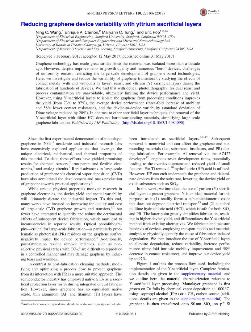
Figure 3 displays a summary of electrical data for the
subset of 44 bare and 56 Y-protected devices fabricated
using Ti/Pd contacts and LOL2000 resist, and the arrows
display the changes between them. Electrical measurements
are taken in vacuum (T¼ 294 K, P 105 Torr) following an
in situ vacuum anneal at 200 C for 1 h, which also reverses
remnant HCl-induced doping (Figs. S5 and S6 in the
FIG. 1. Side-by-side fabrication steps of control (“bare”) graphene devices
and of those protected with the Y sacrificial layer. (a) CVD-grown graphene
is transferred14 onto 90 nm SiO2 on Si after the modified RCA cleaning pro-
cess.7 (b) 5 nm Y deposition via electron beam evaporation. Half of sample
is covered for the control devices. (c) Contact metal photolithography and
subsequent Y removal in dilute DI:HCl in the ratio of 10:1. Some PR resi-
dues remain on control devices. (d) Deposition of the contact metal by elec-
tron beam evaporation (here Ti/Pd or pure Pd). (e) Devices after metal
liftoff. (f) Channel photolithography, Y removal, and graphene removal (O2
plasma). (g) Defined devices after PR removal. (h) Final devices (channel
lengths, L¼ 3 10 lm and widths, W¼ 3 20 lm) after subsequent channel
lithography and final HCl clean. (f) Optical image of the single device which
underwent Y processing.
FIG. 2. (a) Scanning electron micrograph (SEM) of the device after channel
definition and before the final HCl bath. Symbols correspond to acquisition
points for Auger spectroscopy shown in (b). The 1736 eV peak present
only over the channel is lower than known peaks associated with elemental
Y and is indicative of partially oxidized Y.16 An AFM surface comparison
of (c) bare (control) and (d) Y-protected graphene devices in contact regions
after PR development and prior to metal deposition. Using Y-sacrificial
layers decreases the RMS roughness from 1.29 to 0.69 nm.
223106-2 Wang et al. Appl. Phys. Lett. 110, 223106 (2017)
supplementary material). ID vs. VBG measurements (at VDS
¼ 50 mV) as in Fig. 3(a) are then fit to our charge transport
model17,18 using a least-squares method to extract contact
resistance (RC), carrier puddle density (n*), and intrinsic
mobility (l). The total device resistance is R¼ (L/W)RS
þ 2RCþRseries, where RS ¼ [ql(nþ p)]1 is the graphene
sheet resistance, q is the elementary charge, and (nþ p) is
the total carrier concentration which depends on VBG [reach-
ing a minimum at nþ p¼ 2n0 when VBG¼V0, the charge
neutrality point (CNP)].17,18 We note that n0¼ [(n*/2)2
þ nth2]1/2, where n* is the carrier puddle density generated
by ionized impurities, and nth are the thermally generated
carriers.17,18 Thus, at a given temperature, lower n0 means
lower graphene impurity density. RC follows a transfer-
length method (TLM) model,17 and both this and the mobil-
ity are listed at a carrier density of 5 1012 cm2 in the
remainder of this work. Rseries¼ 12 X is our total parasitic
pad, lead, and cable resistance.
Figure 3(a) shows much improved transport in Y-
protected samples, which nevertheless exhibit electron-hole
asymmetry due to cleaner metal-graphene contact interfaces.
(A p-n junction appears at the metal-graphene interface,
increasing the contact resistance for electrons at positive
VBG – V0.19) Figure 3(b) reveals that the Y-sacrificial process
decreases the estimated puddle carrier density n* from
4.6 1011 to 2.2 1011 cm2, which is indicative of a cleaner
graphene surface. In fact, the puddle carrier density of the
Y-protected CVD graphene samples is comparable to that of
previous studies on exfoliated graphene on SiO2.17,18 This is
an important device metric, as it sets a limit on the minimum
GFET current and therefore on the maximum achievable
on/off current ratio. In the ideal case of impurity-free gra-
phene, the minimum carrier density would be given only by
thermally generated carriers, 2n0¼ 2nth 1.6 1011 cm2 at
300 K.18 (Thus, an on/off ratio of >100 could be achieved in
ultra-clean GFETs at room temperature, assuming a maxi-
mum carrier density of >1013 cm2 achieved by strong gating
and negligible contact resistance. To date, the highest GFET
on/off ratios we are aware of are 24 at 300 K and 35 at
250 K, for graphene samples encapsulated by h-BN.20)
In addition, Figs. 3(c) and 3(d) show that average RC
and l improve by factors of 2.5 and 3, respectively
(RC decreases from 4.67 to 1.92 kX lm, while l increases
from 1200 to 3100 cm2 V1 s1). While these values are
for holes, similar improvements in RC and l are also
observed for electron transport (Fig. S7 in the supplementary
material). Table I summarizes the electrical properties and a
yield of 227 measured devices using atmospheric-pressure
CVD graphene, which includes those fabricated with pure-
Pd contacts and using PMGI lift-off resist as well. We use a
conservative definition of yield, i.e., the percentage of devi-
ces with a well-defined, single charge neutrality point (CNP)
V0 and an on/off ratio of >3, where on-current is measured
at maximum negative gate bias (VBG¼30 V) and off-
current is measured at the CNP. This expresses the yield in
terms of electrically “well-behaved” devices, which is a bet-
ter indicator of useful devices than simply the proportion of
electrically active devices.
When comparing the device splits processed without the
Y-protective layer (Table I, LOL2000 resist and Ti/Pd con-
tacts vs. PMGI resist and Pd contacts), only the yield
improves as the number of devices with single CNP
increases for the PMGI process. Since multiple CNPs signify
the presence of charged interface traps,21 the improvement
in the yield is indicative of cleaner graphene interfaces with
the use of PMGI vs. LOL2000, where the contrast-enhancing
dye may leave surface residue. However, despite a more
ideal metal-graphene interface with Pd-only contacts, the
lack of average device performance improvement suggests
that another mechanism is suppressing device performance.
This hypothesis is supported by analyzing the Y-sacrificial
layer devices, which exhibit mobility, impurity density, andcontact resistance improvement over “bare” devices, regard-
less of the metal and/or resist used (Table I). This indicates
that process-induced contamination ultimately limits the per-
formance of graphene devices, and attempts to reduce residue
are insufficient. In other words, graphene must be fullyshielded from fabrication conditions in order to obtain opti-
mal device performance.
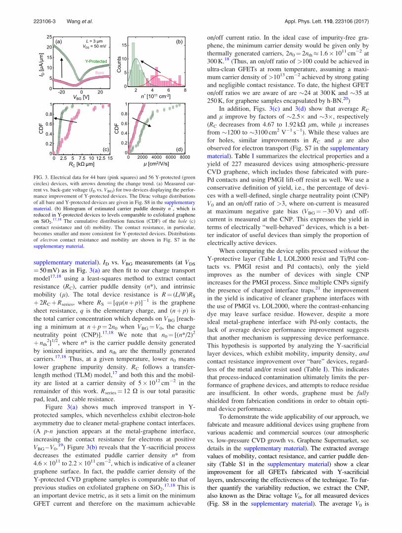
To demonstrate the wide applicability of our approach, we
fabricate and measure additional devices using graphene from
various academic and commercial sources (our atmospheric
vs. low-pressure CVD growth vs. Graphene Supermarket, see
details in the supplementary material). The extracted average
values of mobility, contact resistance, and carrier puddle den-
sity (Table S1 in the supplementary material) show a clear
improvement for all GFETs fabricated with Y-sacrificial
layers, underscoring the effectiveness of the technique. To fur-
ther quantify the variability reduction, we extract the CNP,
also known as the Dirac voltage V0, for all measured devices
(Fig. S8 in the supplementary material). The average V0 is
FIG. 3. Electrical data for 44 bare (pink squares) and 56 Y-protected (green
circles) devices, with arrows denoting the change trend. (a) Measured cur-
rent vs. back-gate voltage (ID vs. VBG) for two devices displaying the perfor-
mance improvement of Y-protected devices. The Dirac voltage distributions
of all bare and Y-protected devices are given in Fig. S8 in the supplementary
material. (b) Histogram of estimated carrier puddle density n*, which is
reduced in Y-protected devices to levels comparable to exfoliated graphene
on SiO2.17,18 The cumulative distribution function (CDF) of the hole (c)
contact resistance and (d) mobility. The contact resistance, in particular,
becomes smaller and more consistent for Y-protected devices. Distributions
of electron contact resistance and mobility are shown in Fig. S7 in the
supplementary material.
223106-3 Wang et al. Appl. Phys. Lett. 110, 223106 (2017)

reduced from 1.22 to 0.89 V, and the standard deviation
decreased from 3.19 to 2.54 V with the Y-sacrificial process.
Given that our test devices are using 90 nm SiO2 as the back-
gate dielectric, the equivalent V0 for 1 nm thin SiO2 would be
0.01 6 0.028 V, very close to the true charge neutrality, signi-
fying that the Y-sacrificial layer technique does not induce
additional doping.
The impact of process-induced contamination on large-
scale GFET fabrication is also evident from the measured
on/off ratios of the subset of atmospheric-pressure derived
graphene devices, as shown in Fig. 4(a). Regardless of the
PR stack or the contact metal, bare devices (without a
Y-sacrificial layer) have higher RC due to process-induced
contamination, yielding a lower on/off ratio at shorter channel
lengths, as RC begins to dominate. This problem is alleviated
with the use of Y-sacrificial layers, which enable cleaner con-
tacts and preserve the on/off ratio down to the shortest channel
lengths used in this study (L¼ 3 lm). In Fig. 4(b), we also
quantify a simple analog device metric, the maximum ratio
of transconductance to current, max(gm/ID), extracted from ID
vs. VBG sweeps. The Y-sacrificial layers improve average
max(gm/ID) by 60%, reflecting an improvement in the chan-
nel quality as the max(gm/ID) is obtained at biases near V0,
where the channel dominates device transport. Since the oxide
is the same for both types of samples, the improvement is
solely from the Y-sacrificial layer technique, reinforcing the
notion that graphene must be protected from PR during proc-
essing to maximize the device performance.
In summary, we introduced a simple and practical
method to improve the graphene device quality through the
use of Y-protective layers during processing. By electrically
characterizing hundreds of graphene devices fabricated under
various conditions, we identify through physical, quantitative
analysis that PR residue restricts device variability and per-
formance. Unlike existing methods, the Y-sacrificial tech-
nique protects the graphene without affecting surrounding
materials, leading to increased device performance, reduced
variability, and increased yield (here up to 97%). Although
demonstrated for GFETs on SiO2, the Y-sacrificial technique
is applicable to other HCl-compatible two-dimensional mate-
rials and substrates, where process contamination could be a
concern.
See supplementary material for further details and the
analysis of the yttrium sacrificial layer process and additional
electrical data.
This work was supported in part by Systems on
Nanoscale Information Fabrics (SONIC), one of the six SRC
STARnet Centers sponsored by MARCO and DARPA, by
the Air Force Office of Scientific Research (AFOSR) under
Grant No. FA9550-14-1-0251, in part by the National
Science Foundation (NSF) EFRI 2-DARE under Grant No.
1542883, and by the Stanford SystemX Alliance. We thank
Ling Li and Professor H.-S. P. Wong for providing the CVD
graphene samples from Graphene Supermarket. We also
thank Sam Vaziri for helpful comments during the
manuscript preparation process.
1K. S. Novoselov, A. K. Geim, S. V. Morozov, D. Jiang, Y. Zhang, S. V.
Dubonos, I. V. Grigorieva, and A. A. Firsov, Science 306, 666 (2004).2P. Yasaei, B. Kumar, R. Hantehzadeh, M. Kayyalha, A. Baskin, N.
Repnin, C. Wang, R. F. Klie, Y. P. Chen, P. Kral et al., Nat. Commun. 5,
4911 (2014); A. Salehi-Khojin, D. Estrada, K. Y. Lin, K. Ran, R. T.
Haasch, J. M. Zuo, E. Pop, and R. I. Masel, Appl. Phys. Lett. 100, 033111
(2012).3S. Lee, K. Lee, C.-H. Liu, G. S. Kulkarni, and Z. Zhong, Nat. Commun. 3,
1018 (2012); R.-H. Kim, M.-H. Bae, D. G. Kim, H. Cheng, B. H. Kim,
D.-H. Kim, M. Li, J. Wu, F. Du, H.-S. Kim, S. Kim, D. Estrada, S. W.
Hong, Y. Huang, E. Pop, and J. A. Rogers, Nano Lett. 11, 3881 (2011).4N. C. Wang, S. K. Gonugondla, I. Nahlus, N. R. Shanbhag, and E. Pop, in
IEEE Symposium on VLSI Technology (2016); S.-J. Han, A. V. Garcia, S.
Oida, K. A. Jenkins, and W. Haensch, Nat. Commun. 5, 3086 (2014).5A. C. Ferrari, F. Bonaccorso, V. Falko, K. S. Novoselov, S. Roche, P.
Bøggild, S. Borini, F. Koppens, V. Palermo, N. Pugno et al., Nanoscale 7,
4598 (2015).6Y. Hao, M. S. Bharathi, L. Wang, Y. Liu, H. Chen, S. Nie, X. Wang, H.
Chou, C. Tan, B. Fallahazad et al., Science 342(6159), 720 (2013); S.
Rahimi, L. Tao, S. F. Chowdhury, S. Park, A. Jouvray, S. Buttress, N.
Rupesinghe, K. Teo, and D. Akinwande, ACS Nano 8(10), 10471 (2014).7X. Liang, B. A. Sperling, I. Calizo, G. Cheng, C. A. Hacker, Q. Zhang, Y.
Obeng, K. Yan, H. Peng, Q. Li et al., ACS Nano 5, 9144 (2011).8R. Shi, H. Xu, B. Chen, Z. Zhang, and L. M. Peng, Appl. Phys. Lett. 102,
113102 (2013).9S. Gahng, C. H. Ra, Y. J. Cho, J. A. Kim, T. Kim, and W. J. Yoo, Appl.
Phys. Lett. 104(22), 223110 (2014).
TABLE I. Average electrical properties (hole mobility, contact resistance, and carrier puddle density) and yield with two types of resists, Ti/Pd vs. pure Pd
contacts, for bare and Y-protected devices. We note that n*¼ 2.2 1011 cm2 corresponds to the puddle surface potential variation D hvF(pn*)1/2 55 meV,
which is comparable to exfoliated graphene devices on SiO2.17,18
LOL2000 resist lithography Ti/Pd contacts PMGI resist lithography Pd contacts
lh (cm2 V1 s1) RC,h (kX lm) n* (cm2) Yield lh (cm2 V1 s1) RC,h (kXlm) n* (cm2) Yield
Bare 1200 4.7 4.6 1011 73% (44/60) 1100 5.5 6.1 1011 85% (55/64)
Y Protect. 3100 1.9 2.2 1011 97% (56/58) 2600 2.2 4.3 1011 93% (42/45)
FIG. 4. (a) Measured on/off ratio of GFETs with various channel lengths
with data laterally scattered for clarity. Pink squares represent bare devices,
and green circles represent Y-protected devices. The latter display up to
3 higher on/off ratio, independent of the channel length due to lower RC.
(b) Y-sacrificial layer also increases the analog GFET figure of merit, the
max(gm/ID) ratio. The low gm/ID values result from thick SiO2 (90 nm)
employed as the gate dielectric, but the relative change due to process condi-
tions is evident.
223106-4 Wang et al. Appl. Phys. Lett. 110, 223106 (2017)

10C. A. Joiner, T. Roy, Z. R. Hesabi, B. Chakrabarti, and E. M. Vogel, Appl.
Phys. Lett. 104, 223109 (2014).11S. Mzali, A. Montanaro, S. Xavier, B. Servet, J.-P. Mazellier, O.
Bezencenet, P. Legagneux, M. Piquemal-Banci, R. Galceran, B. Dlubak
et al., Appl. Phys. Lett. 109(25), 253110 (2016).12A. Hsu, H. Wang, K. K. Kim, J. Kong, and T. Palacios, IEEE Electron
Device Lett. 32, 1008 (2011).13L. Wang, X. Chen, Y. Wang, Z. Wu, W. Li, Y. Han, M. Zhang, Y. He, C.
Zhu, K. K. Fung et al., Nanoscale 5(3), 1116 (2013).14J. D. Wood, G. P. Doidge, E. A. Carrion, J. C. Koepke, J. A. Kaitz, I.
Datye, A. Behnam, J. Hewaparakrama, B. Aruin, Y. Chen et al.,Nanotechnology 26(5), 055302 (2015).
15E. Guerriero, L. Polloni, M. Bianchi, A. Behnam, E. Carrion, L. G. Rizzi,
E. Pop, and R. Sordan, ACS Nano 7(6), 5588 (2013).
16J. M. Baker and J. L. McNatt, J. Vac. Sci. Technol. 9, 792 (1972).17M.-H. Bae, S. Islam, V. E. Dorgan, and E. Pop, ACS Nano 5, 7936 (2011).18V. E. Dorgan, M.-H. Bae, and E. Pop, Appl. Phys. Lett. 97(8), 082112
(2010).19K. Nagashio and A. Toriumi, Jpn. J. Appl. Phys. 50, 070108 (2011); B.
Huard, N. Stander, J. A. Sulpizio, and D. Goldhaber-Gordon, Phys. Rev. B
78(12), 121402 (2008).20L. Wang, I. Meric, P. Y. Huang, Q. Gao, Y. Gao, H. Tran, T. Taniguchi,
K. Watanabe, L. M. Campos, D. A. Muller et al., Science 342(6158), 614
(2013); A. V. Kretinin, Y. Cao, J. S. Tu, G. L. Yu, R. Jalil, K. S.
Novoselov, S. J. Haigh, A. Gholinia, A. Mishchenko, M. Lozada et al.,Nano Lett. 14(6), 3270 (2014).
21A. Di Bartolomeo, F. Giubileo, S. Santandrea, F. Romeo, R. Citro, T.
Schroeder, and G. Lupina, Nanotechnology 22(27), 275702 (2011).
223106-5 Wang et al. Appl. Phys. Lett. 110, 223106 (2017)

Supp.-1
Supplementary Material: Reducing Graphene Device Variability with
Yttrium Sacrificial Layers
Ning C. Wang1, Enrique A. Carrion2, Maryann C. Tung1, Eric Pop1,3,a)
1Department of Electrical Engineering, Stanford University, Stanford, CA 94305, USA
2Department of Electrical and Computer Engineering & Micro and Nanotechnology Lab, University
of Illinois at Urbana-Champaign, Urbana, IL 61801, USA
3Department of Materials Science & Engineering, Stanford University, Stanford, CA 94305, USA
Fabrication Details: Monolayer graphene is first grown on Cu foil (99.8%, Alfa Aesar) via chem-ical vapor deposition (CVD) at 1000 °C in a 1” tube furnace. Two types of growths are conducted, at atmospheric pressure and at 100 mTorr conditions. Atmospheric growths use liquid isopropyl alcohol (IPA, reagent grade) in a metallic bubbler as a carbon source. The bubbler is chilled to 4 °C on a cold plate and 50 SCCM Ar serves as a carrier gas. 250 SCCM of Ar and 50 SCCM H2 are mixed downstream, forming the necessary conditions for growth. Low pressure growths use a gaseous feedstock (100 SCCM CH4) along with 50 SCCM H2 and 1000 SCCM Ar. For both growths, the Cu foil is annealed in growth conditions without carbon sources for 1 hr.
Figure 1 in the main text summarizes the subsequent process steps. After growth, graphene is transferred onto 90 nm SiO2 on p+ Si (< 0.005 Ω⋅cm) by etching the Cu substrate in FeCl3, using a PMMA scaffold for support and applying a modified RCA cleaning process1 to minimize wrinkles and impurities (i.e. Fe, Cl, Cu). As a control in our study, a glass slide raised by silicon spacers shields half of each sample from Y evaporation, creating samples with no sacrificial layer [Fig. 1(b)]. We then fabricate back-gated graphene field-effect transistors (GFETs) using UV photolithogra-phy to define contact and channel regions, HCl to etch the sacrificial Y layer (where necessary), and e-beam evaporation for metal deposition of contacts. We use two different types of PR bi-layer stacks (0.2/1.2 μm LOL2000/Shipley 3612 and 0.2/1.2 μm PMGI/Shipley 3612) in order to assess impact on devices electrical performance, as described in the main text. After PR exposure/development and Y etching (samples are immersed in a dilute 10:1 deionized water DI:HCl solution for 15 s, although the photoresist survives baths up to 180 s without affect-ing feature definition), we deposit 1.5/40 nm Ti/Pd via e-beam evaporation (~10-7 Torr) as contact metal. A separate set of devices using 40 nm Pd without a Ti interfacial layer was fabricated to study the impact of interfacial Ti adhesion layers on contact resistance. After 1 hour liftoff in Remover PG, we proceed with photolithography for channel definition (length L = 3−10 µm and width W = 3−20 µm). Finally, Y is removed in open regions after resist development to expose the underlying graphene to a subsequent O2 plasma etch (100 SCCM O2, 150 mTorr, 250 W) for graphene removal and channel definition. Finally, all Y is removed prior to device measurements with a prolonged 60 second dilute DI:HCl bath.

Supp.-2
Figure S1. 20x optical images of initial graphene on SiO2 sample, after 5 and 10 nm Y deposition, and after baking on a hot plate in air at 110 °C for 1 minute. Although residue spots are present on all samples, the spots are present on the initial graphene and are therefore not a result of the Y deposition. The hot plate step induces irreversible cracks in the 10 nm Y film, which can also affect the underlying graphene, most likely as a result of rapid oxidation and mismatches in coefficient of thermal expansion. However, the thinner ~5 nm Y film is unaffected, and thus we suggest keep-ing Y films < 5 nm to prevent cracking. Additional measures, such as baking in an inert environ-ment, must be taken if a thicker film is necessary to prevent damage to graphene.
Figure S2. (a) SEM of device, followed by full Auger mapping of channel region after contact metallization and prior to final Y removal (Phi Instruments, 5 keV, 10 nA). (b) Yttrium mapping is averaged over 20 scans, while (c) oxygen and (d) carbon mappings are integrated over 5. Sig-nificant Y signal is present only in the channel in figure (b), confirming removal of Y in desired regions as well as remaining Y protecting the channel.

Supp.-3
Figure S3. Tapping mode AFM (Digital Instruments) of Ti/Pd contacts (a) before and (b) after exposure to 10:1 DI:HCl for 15 seconds. Minimal Pd metal (~1 nm) is removed with the diluted solution, confirming a high etch selectivity (~ 3:1) to Y over surrounding contact metal.
Figure S4. Raman spectroscopy (WiTec 532 nm laser) of graphene under defined contact region (a) before and (b) after Y removal in 10:1 DI:HCl. No noticeable increase in D-peak is observed after Y deposition, nor after HCl etch, confirming that the Y-sacrificial layer processing is safe for graphene. The G-peak is blue-shifted after exposure to HCl, indicative of some doping; however, this doping effect is reversible, as shown in Fig. S5.

Supp.-4
Figure S5. Electrical measurement of back-gated GFET before and after channel doping in 2:1 HCl for 1 second. Undoped device is shown as grey squares, while doped measurements are shown as pink circles. The doping effect is largely reversed by a 200 °C anneal in vacuum for 2 hours.
Figure S6. Electrical measurements (in ~10-5 Torr vacuum) of back-gated GFET (a) with and (b) without 2:1 HCl treatment for 180 seconds. HCl treated devices exhibit (c) lower charge puddle concentration (n*) than untreated devices, implying that the HCl treatment cleans the graphene surface, although (d) mobility is largely unaffected. (e) Untreated and (f) HCl treated devices ex-hibit slightly (g) lower charge puddle concentration with further vacuum annealing (2 hours, 200 °C). (h) Annealing improves hole transport similarly for untreated and HCl treated devices. Device channel length (L) is 2 μm and widths (W) range from 5 – 10 μm.
-40 -20 0 20 400
10
20
30
40
50
R x
W [
k x
m
]
VBG[V]-40 -20 0 20 40
0
10
20
30
40
50
R x
W [
k x
m
]
VBG[V]
Untreated HCl Doped
20 ⁰C
~ 5.5x
(a)
Si (p++)
SiO2 (90 nm)
VD VS
VG
L
W
VBG

Supp.-5
Figure S7. Cumulative distribution function (CDF) of electron contact resistance and mobility for devices with Ti/Pd contacts. 44 bare (pink squares) and 56 Y-protected (green circles) samples measured. Similar to hole transport (main text Fig. 3), electron transport properties improve as well with use of Y-sacrificial layers as (a) average RC decreases from 7.4 to 4.3 kΩ-μm and (b) average μ increases from 1792 to 3730 cm2V-1s-1.
Figure S8. Histogram of charge neutrality point (CNP) i.e. Dirac voltage V0 for all 378 devices measured in this study. The dashed red line for bare devices and the solid green line for Y protected devices represent fitted Gaussian distributions. The average V0 is reduced from 1.22 to 0.89 V and the standard deviation decreased from 3.19 to 2.54 V with the Y-sacrificial process. These values are measured on 90 nm SiO2 back-gate oxide, thus values for ~1 nm equivalent oxide thickness (EOT) would be reduced by a factor of 90x (see main text).
0 5 10 15 20 250
0.2
0.4
0.6
0.8
1
0 2000 4000 6000 80000
0.2
0.4
0.6
0.8
1(a) (b)
CD
F
CD
F
RC [kΩ-µm] µ [cm2/V/s]
-10 -5 0 5 100
5
10
15
20
25
30
35
V0 [V]
Cou
nts
Supp.-6
Table S1. Average values of electrical data (electrons, holes, mobility, contact resistance, puddle charge density, CNP voltage) for all 378 GFETs fabricated from various graphene sources.
µe
[cm2V-1s-1] Μh
[cm2V-1s-1] RC,e
[kΩ-µm]RC,h
[kΩ-µm]n*
[cm-2] V0 [V]
Stanford University (Atmospheric Pressure CVD)
Bare 1800 1200 7.4 4.7 4.6×10¹¹ -1.4
Y-Sacr. 3700 3100 4.3 1.9 2.2×10¹¹ -0.8
University of Illinois Urbana-Champaign (Low Pressure ~100 mTorr CVD)
Bare 2100 1270 10.2 6.1 5.0×10¹¹ 2.5
Y-Sacr. 3000 2700 6.4 3.5 2.8×10¹¹ 0.6
Graphene Supermarket
Bare ---* ---* 17.9 4.3 7.3×10¹¹ 13.5
Y-Sacr. 3700 2300 4.3 1.3 4.6×10¹¹ 6.1 *Data not shown due to poor fit.
1 X. Liang, B.A. Sperling, I. Calizo, G. Cheng, C.A. Hacker, Q. Zhang et al., ACS Nano 5, 9144 (2011).


![Yttriga, INN- Yttrium [90Y] chloride](https://static.fdocuments.net/doc/165x107/588c5b3a1a28abfe208b604f/yttriga-inn-yttrium-90y-chloride.jpg)