RECOMMENDATIONS TO THE GOVERNMENT OF KARNATAKA TOWARD …€¦ · · 2016-05-13RECOMMENDATIONS TO...
29
Page 1 RECOMMENDATIONS TO THE GOVERNMENT OF KARNATAKA TOWARDS THE STATE SEMICONDUCTOR POLICY India Semiconductor Association August, 2008 This document sets out a series of measures and initiatives that could be considered by the Government of Karnataka to attract significant investments to Karnataka in the semiconductor space
Transcript of RECOMMENDATIONS TO THE GOVERNMENT OF KARNATAKA TOWARD …€¦ · · 2016-05-13RECOMMENDATIONS TO...

Page 1
RECOMMENDATIONS TO THE GOVERNMENT OF KARNATAKA TOWARDS THE STATE SEMICONDUCTOR
POLICY
India Semiconductor Association
August, 2008
This document sets out a series of measures and initiatives that could be considered by the Government of Karnataka to attract significant investments to Karnataka in the semiconductor space

Page 2
‘ISA Confidential – For Private Circulation Only’
RECOMMENDATIONS TO THE GOVERNMENT OF KARNATAKA TOWARDS THE STATE
SEMICONDUCTOR POLICY
1. Introduction 3
1.1. About India Semiconductor Association (ISA) 3
2. Semiconductor industry 4
2.1. Semiconductor design and manufacturing 4
2.2. Solar PV manufacturing 7
3. Government of India’s (GoI) Semiconductor Policy, 2007 8
3.1. Current status 8
4. Objective of this proposal 10
5. Need for a Karnataka specific Semiconductor Policy 11
6. Key activities to be undertaken - Semiconductor design 12
6.1. Develop tier 2 cities, satellite towns in Karnataka as design clusters 12
6.2. Incentives for the design sector 13
7. Key activities to be undertaken - Semiconductor manufacturing 15
7.1. Focus on attracting investments in Solar PV manufacturing 15
7.2. Promote Karnataka as a destination for ATMP and ancillary units 16
7.3. Attract investments for a wafer fabrication facility 16
7.4. Build manufacturing clusters for the hi tech manufacturing sector 17
7.5. Incentives for the manufacturing sector 18
8. Key activities to be undertaken to promote Green Energy 22
8.1. Promote development of solar farms 22
8.2. Encourage use of solar energy 24
8.3. ‘Core group’ to promote the cause of solar in the Government 24
9. Focus on manpower development 24
9.1. Need to build domain expertise 25
10. Summary of recommendations 27
11. Conclusion 29

Page 3
‘ISA Confidential – For Private Circulation Only’
1. Introduction
1.1. About India Semiconductor Association (ISA) ISA is the trade body representing the Indian semiconductor driven industry. ISA has around 130 members from the semiconductor driven industry from India and outside it as also its ecosystem. These include design companies, solar fabs, manufacturing companies and others in the ecosystem like venture funds, legal and IP firms. ISA is committed towards building global awareness for the Indian semiconductor driven industry and supporting its growth through focused activities. It has global alliances including focussed collaborations in the US and Taiwan to further the interests of its members. These collaborations are with Taiwan Semiconductor Industry Association (TSUA), Global Semiconductor Alliance (GSA), Semiconductor Equipment and Materials International (SEMI) ISA has played a prominent role in supporting the Government of India in the Semiconductor Policy. It is also involved with State Governments.
Vision ISA’s vision is to establish India as the preferred global hub for excellence in creation of semiconductor products through technology leadership.
Mission The primary objective of ISA is to act as a catalyst for the growth of the semiconductor industry in India. Other objectives include:
· Create global awareness for Indian semiconductor industry outside of the generic “IT” umbrella
· Create a win-win interaction amongst semiconductor product and services companies, government, academia, venture capitalists and industry bodies
· Create an enabling ecosystem that catalyzes industry’s growth and leadership · Foster active collaboration between industry, universities and government to further
expand the available world-class semiconductor talent pool · Identification of investment opportunities · Drive technology vision for the semiconductor industry · Promotion of trade and industry

Page 4
‘ISA Confidential – For Private Circulation Only’
2. Semiconductor industry
2.1. Semiconductor design and manufacturing Overview Semiconductor design includes VLSI design, hardware/board design and embedded software development. In India, it is done by the subsidiaries of multinational companies such as Texas Instruments, Intel, etc and by domestic companies such as Wipro, Mindtree, among others.
Captive (US$ mn)
Captive percentage
Non-captive (US$ mn)
Non-captive percentage
Total Revenues (US$ mn)
VLSI 361.15 62% 221.35 38% 582.5
Hardware/ Board
40.5 29% 99.3 71% 139.8
Embedded Software
733.7 29% 1796.3 71% 2530
Semiconductor manufacturing consists of the following stages:
· Production of silicon wafers from very pure silicon ingots; · Fabrication of integrated circuits onto these wafers; · Assembly of every integrated circuit on the wafer into a finished product; and · Testing and back-end processing of the finished products.
Wafer Fabrication: Wafer fabrication generally refers to the process of building integrated circuits on silicon wafers.
Assembly, Testing, Marking and Packing (ATMP): The process of putting the integrated circuit inside a package to make it reliable and convenient to use is known as semiconductor package assembly, or simply 'assembly'. Over the years, the direction of assembly technology has been to develop smaller, cheaper, more reliable and environment-friendly packages. Technology advancements allow for a choice of packages.
Global outlook The global semiconductor market was around US $ 275 billion (bn) in 2007 and is expected to reach US $ 311 bn in 2008. Chip design accounts for nearly 30% of the semiconductor business with total revenue of over US $ 80 bn. Chip manufacturing and ATMP (Assembly, testing, marking and packing) account for the remaining 70%. (Source: Gartner and World semiconductor statistics, 2007).

Page 5
‘ISA Confidential – For Private Circulation Only’
Indian scenario
Semiconductor design Design is the core strength of India’s semiconductor industry. There are around 200 companies (domestic and multinational subsidiaries) in this area in India. Most global semiconductor design companies have a presence here. The design industry includes VLSI design, board design and embedded software market. Annual revenues are estimated at US $ 6.08 bn (ISA-IDC Report 2008). Over 80% of the revenues in semiconductor design in India are from embedded software.
Revenues and employment (2007/10):
Total design market
Year 2007 Year 2010
Revenues in US$ bn (Share of
total in %)
Engineering workforce in nos (Share of total
in %)
Revenues in US$ bn (Share of total in %)
Engineering workforce in nos
(Share of total in %)
VLSI 0.77 (13%) 13,996 (11%)
1.13 (13%)
19,637 (11%)
Hardware/ Board Design
0.38 (6%) 9421 (7%)
0.56 (6%)
12,923 (7%)
Embedded Software
4.93 (81%) 106,579 (82%)
7.28 (81%)
149,976 (82%)
Total 6.08 (100%) 129,996 (100%)
8.97 (100%)
182,536 (100%)
CAGR for revenues: 21.7% (2007-10); CAGR for workforce: 19% (2007-10) Source: ISA-IDC report, 2008
India has emerged as a strong base for design and development centres for semiconductor multinational companies. Indian Design Centres (IDCs) have graduated from executing small projects to driving critical and complex ones. It is becoming increasingly common to find leading edge designs for the global market being driven by these IDCs. In addition, IDCs provide global support on tools and methodology. 23 of the top 25 semiconductor companies have operations in India. (Source: iSuppli report, 2008).
The design market has grown significantly due to the increasing number of international companies setting up offshore design and development centres in India and through expansion of current centres. Factors driving this market are as follows:
· Market need for regular introduction of new product variants and models has forced original equipment manufacturers (OEMs) and product companies to seek reduction in product development cycle time through outsourcing arrangements
· Declining margins and R&D budgets have driven companies to look for cost effective solutions without compromising on the quality of work

Page 6
‘ISA Confidential – For Private Circulation Only’
· Availability of a large base of engineering workforce coupled with their proficiency in English, has made India an attractive destination for design and development
· EDA companies (both product and service) are the starting block for the VLSI and hardware/ board design market. They are important links in the semiconductor value chain.
Industry leaders believe that India is becoming a ‘design store’ with strengths in intellectual property (IP) development, integration and embedded system services.
Design activities are clustered in four major cities of India. The largest cluster is in Bangalore, followed by Hyderabad, Delhi NCR and Chennai. Bangalore has around 85 of these firms (including multinationals) engaged in semiconductor related design in India – making it one of the major global clusters in chip design, along with the Silicon Valley (USA), Cambridge UK and Taiwan. India’s competitive edge in the global market is its talent base with design capabilities. Global companies are aware of the availability of this talent pool and are leveraging it effectively.
Semiconductor manufacturing The Indian semiconductor market in 2007 was estimated at US $ 3.47 bn. (Source: ISA & Frost & Sullivan report Update 2007-08). Telecommunications, Information technology, Office automation (IT & OA) and Consumer Electronics contributed to 82.6% of the market for semiconductors in India. Growth is expected to be driven by end products such as mobile handsets, desktops and notebooks, GSM base stations, set top boxes and energy meters.
Total Market (TM), which reflects total consumption, is growing at a CAGR of around 27% whereas Total Available Market (TAM), which reflects local consumption in manufacturing, is growing at a CAGR of 36%, clearly showing that local manufacturing will grow in India substantially in the next few years. The following table shows the TM and TAM numbers and their CAGR during 2006-09.
Indian semiconductor market: Revenue forecasts in US $ bn, 2009
Year 2006 Year 2009 CAGR (2006-09)
TM 2.69 5.49 27%
TAM 1.26 3.18 36%
Year 2007: TM – US $ 3.47 bn; TAM – US $ 1.74 bn; Source: ISA-Frot & Sullivan update report 2007-08
India's total semiconductor consumption is primarily serviced by imports.

Page 7
‘ISA Confidential – For Private Circulation Only’
While India is recognised for its design capabilities, chip manufacturing in India on the other hand, has been restricted to captive centres for defence and aerospace. Asian countries such as China, Japan, Korea, Malaysia, Singapore and Taiwan have been the preferred outsourced partners for chip fabrication, assembly, test and packing, primarily because the countries had envisioned a National Agenda to promote the semiconductor industry through proactive policies like China 863 National Plan, Japan STARC, Korea IT 839, Malaysia 2020 and SOC Taiwan. Approximately 40% of the global wafer fab capacity is located in these East Asian countries excluding Japan, which accounts for another 24% of the worldwide wafer fab capacity. US accounts for around 16% of the wafer fab capacity. (Source: www.semi.org)
Semiconductors are recognized as the technology enabler for the entire electronics value chain. The growing electronics market in India has attracted global Electronic Manufacturing Services (EMS) players to India. Leaders in EMS like Elcoteq, Flextronics, Foxconn, Jabil, Solectron and many more have made large investments to address the Indian market. While EMS is expected to grow and drive demand for chips, India is yet to make strides in high tech manufacturing. Hi Tech manufacturing is non-existent in the country. The semicon policy of Government of India is expected to boost investment in this sector
2.2. Solar PV manufacturing The type of equipment used in solar fabs is similar to that used in semiconductor fabs (CVD, PVD, Etch, etc), except for a few minor changes depending on whether one is in the Crystalline-Silicon (c-Si), or the Thin-Film (TF), arena. Hence, the solar cell manufacturing industry is interdependent with the semiconductor manufacturing industry and will help develop the semiconductor ecosystem in India. Given the spiralling oil prices and a finite supply of coal based reserves, there is the need to harness indigenous renewable sources and solar is emerging as a viable alternative. India produced only 45 MWp of solar cells and 80 MWp of modules in 2006-07 (Source: MNRE – Annual Report 2006-07). Nearly 80% of the country’s production of these products is currently being met by manufacturing facilities that are located in the State (Source: MNRE – Annual report, 2006-07), which is however not universally known. In 2007-08, the MNRE estimates the Solar PV industry production at 140 MW for solar cells and 175 MW of solar PV modules.

Page 8
‘ISA Confidential – For Private Circulation Only’
3. Government of India’s (GoI) Semiconductor Policy, 2007 The Semiconductor Policy announced by Government of India in 2007 provides special incentive package to attract investments for setting up semiconductor fabrication and other micro and nanotechnology manufacturing industries. The incentives will be for the manufacture of all semiconductors, displays including Liquid Crystal Displays, Organic Light Emitting diodes, Plasma display panels and any other emerging displays, storage devices, solar cells, photo voltaic and other advanced micro and nanotechnology products and assembly and test.
A key benefit is the grant of the SEZ status. The special incentive package shall be available only up to 31.3.2010
Types of unit Threshold NPV of investments
Incentives in SEZ
Incentives in Non – SEZ
Fab unit Rs.2,500 crores (US$ 625 mn) 20% 25% + exemption from CVD
Eco system unit Rs.1,000 crores (US$ 250 mn) 20% 25% + exemption from CVD
Note: (Incentive in % of capital expenditure); CVD is Countervailing Duty; I US$ = Rs. 40
3.1. Current status The announcement of the Semiconductor Policy 2007 is expected to attract investment in manufacturing, its eco system and related high tech manufacturing. Proposals more than Rs. 98,000 crores (US $ 24.73 bn) have been received till date (Source: DIT July 2008). The summary of the proposals received to date is as follows:
Investor name Product Total investment
Rs. Crores Equivalent US $ bn
M/s Videocon Industries Ltd LCD Fab – TFT Flat panel display: G6 type plant
8,000 2.00
M/s Moser Baer PV Technologies India Ltd
Silicon cells, modules, thin film concentrators
6,000 1.50
M/s Titan Energy System Ltd. Solar cells, Solar grade semiconductor wafer, SPV modules & Polysilicon
5,880 1.47
M/s KSK Energy Ventures Private Limited
Integrated Solar panel based on thin film and CdTe Technology
3,211 0.80
M/s Signet Solar Inc. Solar PV & associated products: Thin film based
9,672 2.42
M/s Reliance Industries Ltd. Solar PV – Polysilicon, Wafers, Cells and Modules
11,631 2.91
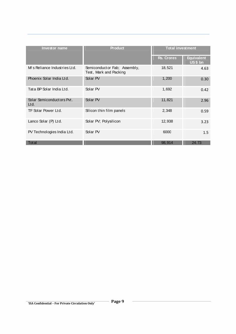
Page 9
‘ISA Confidential – For Private Circulation Only’
Investor name Product Total investment
Rs. Crores Equivalent US $ bn
M/s Reliance Industries Ltd. Semiconductor Fab; Assembly, Test, Mark and Packing
18,521 4.63
Phoenix Solar India Ltd. Solar PV 1,200 0.30
Tata BP Solar India Ltd. Solar PV 1,692 0.42
Solar Semiconductors Pvt. Ltd.
Solar PV 11,821 2.96
TF Solar Power Ltd. Silicon thin film panels 2,348 0.59
Lanco Solar (P) Ltd. Solar PV; Polysilicon 12,938 3.23
PV Technologies India Ltd. Solar PV 6000 1.5
Total 98,914 24.73

Page 10
‘ISA Confidential – For Private Circulation Only’
4. Objective of this proposal Traditionally, Karnataka has been the favoured destination for the technology sector-in software, semiconductors and biotechnology. Bangalore has been a preferred hub of the GoI defence labs. This coupled with the talent pool, access to engineering colleges and attractiveness as an investment destination for private sector companies, has created an ecosystem giving Karnataka a national edge.
Bangalore is the largest hub of semiconductor design companies, outside the Bay Area in California. Nearly 70% of the country’s chip designers work here and around 80% of the sector’s revenues in design are from this city alone.
In the last few years, other states, including Andhra Pradesh, Tamil Nadu, Maharashtra and Gujarat, have been attracting fresh investments in the semiconductor industry through industry friendly policies and investments in infrastructure. Karnataka runs the risk of losing its leadership position unless it takes proactive measures to attract and retain investment.
This document sets out a series of measures and initiatives that should be considered by the Government of Karnataka (GoK) to attract significant investments to Karnataka in the semiconductor space.

Page 11
‘ISA Confidential – For Private Circulation Only’
5. Need for a Karnataka specific Semiconductor Policy As on date, proposals worth more than Rs. 98,000 crores (US$ 24.73 bn) have been received in the area of semiconductor related manufacturing. However, none of these firms appears to be considering Karnataka as an investment destination. Andhra Pradesh and Tamil Nadu, which have both offered additional incentives and subsidies to woo firms, have taken the lead here. Andhra Pradesh is attracting investments in the space of solar photovoltaic manufacturing. Tamil Nadu on the other hand, has become the manufacturing hub in the South and has carved a niche for itself in the EMS space.
Karnataka has to take two important steps
a) Retain its edge in design by attracting fresh investments and expansion by existing companies within the state.
b) Attract manufacturing related investments
This proposal focuses on the steps to be taken by the Government of Karnataka to enable the same. Government of Karnataka needs to focus on 3 key activities
I) Promote Karnataka as a semiconductor design hub II) Attract investments in high-tech semiconductor manufacturing III) Promote generation and use of green energy – specifically solar energy IV) Focus on manpower development

Page 12
‘ISA Confidential – For Private Circulation Only’
6. Key activities to be undertaken - Semiconductor design Karnataka needs to retain its edge in the design services business by providing specific incentives to design services start ups. While Bangalore can continue to be the key centre in the state, tier 2 cities in the state should be developed to attract investments.
6.1. Develop tier 2 cities, satellite towns in Karnataka as design clusters Karnataka has been the forerunner in the IT/ITeS space owing to an appropriate ecosystem for knowledge-driven industries, including proactive government, sector-friendly policy and a large pool of skilled manpower. IT & ITeS sector accounts for 25% of Karnataka’s Gross State Domestic Product GSDP of $47.32 bn in 2006-2007. As per STPI, semiconductor design and development constitutes a key element of IT revenues.
Apart from Bangalore, the other emerging destinations for the design sector are Mysore, Mangalore and Hubli. Mysore with software export revenues of Rs. 760 crores (US$ 190 mn) is emerging as an alternative destination to Bangalore in service and tourism sectors. 49 firms are registered with the STPI in Mysore. A cargo airport is expected to be commissioned here soon. With the opening up of the 111 km BMIC corridor, travel time is likely to reduce further. Mangalore with software export revenues of Rs. 681 crores ( US $ 170 mn) is a fast emerging hub for logistics, manufacturing and services, with 24 firms currently registered with Mangalore STPI. It also has the added advantage of an international airport and seaport. Hubli is now becoming the choice of IT and ITeS firms with 13 firms registered with STPI and revenues of Rs. 0.85 crores (US$ 0.21 mn). All three cities are centres of educational institutions with 5 major universities being headquartered in these three locations. This cluster generates sizeable revenues from software and its further development should be taken up by the Government of Karnataka. Some details of these centres are set out below:
City Software export revenues (Rs. crores) (US $ mn)
No. of Engg.
Colleges
Proposed SEZs
2004-2005 2005-2006 2006-2007 CAGR
Mysore 309 (77) 392 (98) 760 (190) 56.8% 6 3
Mangalore 567 (141) 570 (142) 681 (170) 9.6% 11 6
Hubli 0.035 (0.008) 0.050 (0.012) 0.085 (0.021) 55.8% 2 1
Source: STPI web site, IBEF H
Karnataka needs to leverage its access to academic talent and the available technology domain expertise and focus on developing tier 2 cities such as Mysore, Mangalore and Hubli.
Page 13
‘ISA Confidential – For Private Circulation Only’
6.2. Incentives for the design sector
6.2.1. Fund for silicon design start-ups Currently, the Government of Karnataka renders financial assistance to start-ups through the Karnataka Information Technology Venture Capital Fund (KITVEN Fund). KITVEN fund is an Information Technology specific Rs. 15 crores (US $ 3.75 mn), fund registered with Securities & Exchange Board of India (SEBI).
KITVEN Fund helps the early stage investor, extending support services to companies mainly in the areas of financial strategies, business strategies, internal controls, management information system etc. The Fund has invested in 17 companies with investment of more than Rs.12 crores (US $ 3 mn). Some of the assisted companies have grown in size and KITVEN Fund has exited from 13 companies.
This fund should be made available to chip design and embedded software firms too. Limits however could be revised upwards to be in line with investment levels in start up organisations in the industry. A start up firm with 15 employees would need funds in the range of Rs. 2-3 crores (US $ 0.5 – 0.75 mn), in year 1.
Government of Karnataka should set up a start fund of Rs. 50 crores (US $ 12.5 mn) under the KITVEN fund to assist design services firms
6.2.2. Subsidise IP filing cost Focusing on start-ups will help Karnataka attract investments in the design space, promote IP creation. Government of Karnataka should also provide financial assistance to firms for filing IP.
50% subsidy on IP filing costs for companies of Indian origin alone to be provided
6.2.3. Set up characterisation lab at Orchid Tech space STPI-Bangalore and the Karnataka Government, with support from the industry, were the first in India to open a world-class incubation centre in June 2006, with an investment of Rs. 9.2 crores ($2.3 mn). The Orchid Tech space integrated incubation centre is meant to create opportunities for entrepreneurs. The state-of-the-art centre, which can support 10 companies at a time, works closely with the Indian Semiconductor Association (ISA) and The Indus Entrepreneurs (TiE) to incubate tech start-ups and firms.
The Government of Karnataka should focus on attracting entrepreneurs to use the state of the art facilities provided by this incubation centre. With the state-of-the-art facilities, including high-end desktops, servers, data centre and an international gateway, the incubation centre encourages and facilitates innovation without the constraints of capital investment.

Page 14
‘ISA Confidential – For Private Circulation Only’
The infrastructure at Orchid Tech space needs to be augmented to that of a characterisation lab, with equipment such as logic analysers, spectrum analysers, oscilloscope, etc, which are required by design services firms to test their designs, etc. and design tools which account to
Provide Rs. 20 crores (US $ 5 mn) for setting up the characterisation lab at the Orchid Incubation Centre

Page 15
‘ISA Confidential – For Private Circulation Only’
7. Key activities to be undertaken - Semiconductor manufacturing The semiconductor industry is widely recognised as the key driver for economic growth, besides acting as a technology enabler for the entire electronics value chain. Karnataka should draw up initiatives to set up an entire eco system which would provide the infrastructure and incentives for attracting investments in the areas of Solar PV cell manufacturing; ATMP facilities; Wafer fabrication facility. Building a manufacturing cluster will facilitate development of the industry
7.1. Focus on attracting investments in Solar PV manufacturing Rationale for promoting investments in solar PV:
· The investments are lower at about $ 200 million for a 100 MW line, when compared to semiconductor fabs, which are upward of $ 3 bn
· Solar energy being clean energy could attract further investments – especially if the government policies are attractive, including the provision of subsidies/incentives based on generation based incentives, equipment used and land.
· Demand for solar cells/modules/systems is expected to increase, both from export and domestic markets.
Karnataka has a clear early mover advantage in this arena. It has emerged as a hub for the manufacture of solar energy products such as solar water heating systems, solar photovoltaic modules and systems and various components required by the renewable energy sector. With the proactive promotion activities implemented by other states, Karnataka is losing this advantage and could cease to attract further investment. Post the announcement of Government of India’s semiconductor policy and aggressive initiatives shown by neighbouring states, new investors are considering Andhra Pradesh, Tamil Nadu and other states as their destinations for solar PV production. Government of Karnataka hence needs to work towards retaining its leadership position and attracting the large investments announced in this field.
The recent investments seen in solar PV manufacturing are essentially from large players looking at both the domestic and export markets - Reliance, Moser Baer, Signet Solar, Solar Semiconductors, etc. These firms are likely to initially focus on export markets. As the cost of power generation from solar PV route reduces further, India itself could emerge as a market for solar energy, given the high solar incidence in India and the initiatives being taken by the government.

Page 16
‘ISA Confidential – For Private Circulation Only’
7.2. Promote Karnataka as a destination for ATMP and ancillary units Semiconductor assembly, testing, marking and packing process (ATMP) is challenging, but is presently a more viable option to front-end manufacturing in India.
Building a state of the art semiconductor fabrication facility requires high capital investment, access to technology, skilled manpower with experience on foundry process and customers willing to devote resources to switch over to a new vendor. A latest estimate states that chip fabrication needs an investment of US $3 bn or more and will continue to go up with each new technology process.
IC assembly involves a different and lower order of complexity than what is required in front end wafer processing. ATMP location and processes are independent of wafer fabrication units and can therefore be located anywhere in the world. Investments vary with the product and capacity and could range anywhere between US $ 100 to 500 mn for large capacity plants.
India offers an advantage in terms of availability of low cost talent and not necessarily only engineers. An ATMP facility in India could import wafers, assemble and after final testing, ship the final device directly to customers—who are largely in Asia itself.
If Karnataka becomes the hub for ATMP facilities, the state would become the preferred destination for the fab companies to invest in chip manufacturing.
7.3. Attract investments for a wafer fabrication facility Wafer fabrication is a highly capital intensive activity and a state of the art wafer fab could cost around $3 bn for a single fabrication unit and assuming a 2:1 debt equity ratio, such a unit could require up to US $ 1 bn in equity investments. Given that India is a late entrant and does not have a ready infrastructure to attract such large investments, strong encouragement from the government is required to draw the first set of investors to commit to such large investments. This will also be viewed as Government’s commitment towards funding the foundation of this sector.
The industry is also characterised by long gestation periods with typical breakeven periods being in the order of 8-10 years. Government support is very critical in the initial stages.
Setting up a fab facility is likely to result in long term benefits in terms of employment generation, increased inflow of foreign investments into the state and increased manufacturing activity. Each wafer fab facility would result in the establishment of 15 ancillary units. Local semiconductor manufacturing will also spur investments in electronics equipment / products manufacturing.
Governments of China, Taiwan and Singapore have extended extensive support to manufacturing units in their countries. Highlights of these government initiatives and support is given below
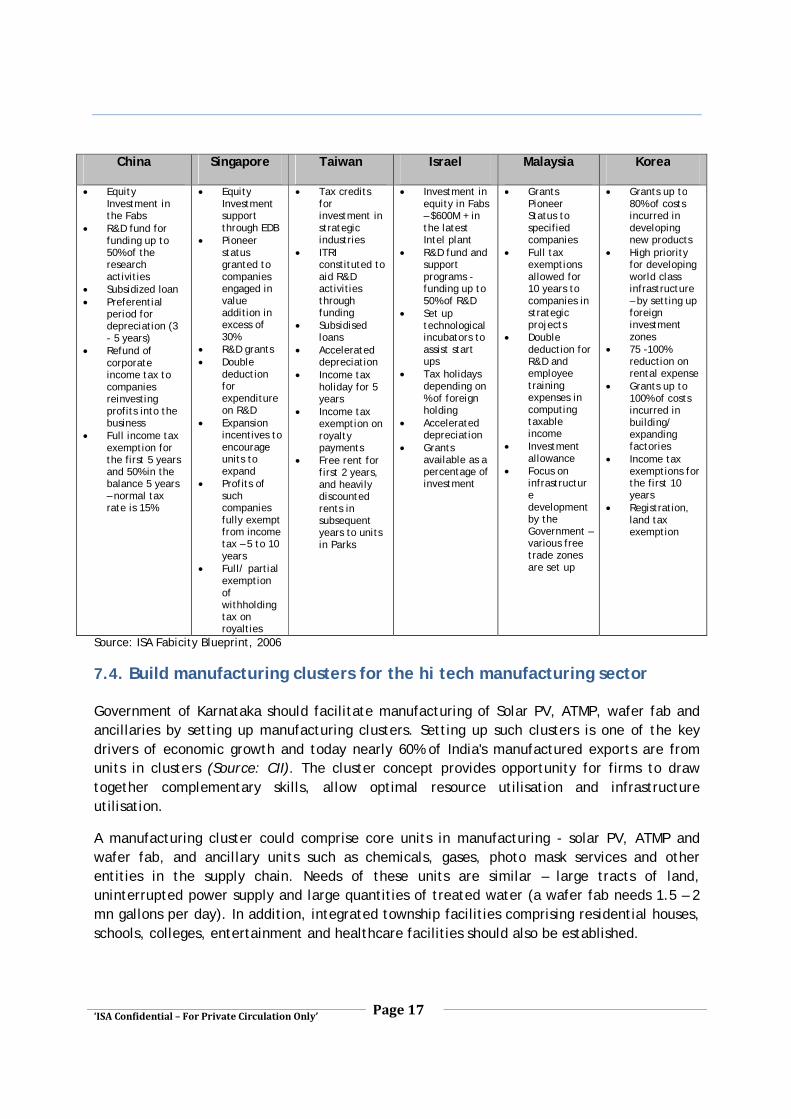
Page 17
‘ISA Confidential – For Private Circulation Only’
China Singapore Taiwan Israel Malaysia Korea
· Equity Investment in the Fabs
· R&D fund for funding up to 50% of the research activities
· Subsidized loan · Preferential
period for depreciation (3 - 5 years)
· Refund of corporate income tax to companies reinvesting profits into the business
· Full income tax exemption for the first 5 years and 50% in the balance 5 years – normal tax rate is 15%
· Equity Investment support through EDB
· Pioneer status granted to companies engaged in value addition in excess of 30%
· R&D grants · Double
deduction for expenditure on R&D
· Expansion incentives to encourage units to expand
· Profits of such companies fully exempt from income tax – 5 to 10 years
· Full/ partial exemption of withholding tax on royalties
· Tax credits for investment in strategic industries
· ITRI constituted to aid R&D activities through funding
· Subsidised loans
· Accelerated depreciation
· Income tax holiday for 5 years
· Income tax exemption on royalty payments
· Free rent for first 2 years, and heavily discounted rents in subsequent years to units in Parks
· Investment in equity in Fabs – $600M + in the latest Intel plant
· R&D fund and support programs - funding up to 50% of R&D
· Set up technological incubators to assist start ups
· Tax holidays depending on % of foreign holding
· Accelerated depreciation
· Grants available as a percentage of investment
· Grants Pioneer Status to specified companies
· Full tax exemptions allowed for 10 years to companies in strategic projects
· Double deduction for R&D and employee training expenses in computing taxable income
· Investment allowance
· Focus on infrastructure development by the Government – various free trade zones are set up
· Grants up to 80% of costs incurred in developing new products
· High priority for developing world class infrastructure – by setting up foreign investment zones
· 75 -100% reduction on rental expense
· Grants up to 100% of costs incurred in building/ expanding factories
· Income tax exemptions for the first 10 years
· Registration, land tax exemption
Source: ISA Fabicity Blueprint, 2006
7.4. Build manufacturing clusters for the hi tech manufacturing sector Government of Karnataka should facilitate manufacturing of Solar PV, ATMP, wafer fab and ancillaries by setting up manufacturing clusters. Setting up such clusters is one of the key drivers of economic growth and today nearly 60% of India's manufactured exports are from units in clusters (Source: CII). The cluster concept provides opportunity for firms to draw together complementary skills, allow optimal resource utilisation and infrastructure utilisation.
A manufacturing cluster could comprise core units in manufacturing - solar PV, ATMP and wafer fab, and ancillary units such as chemicals, gases, photo mask services and other entities in the supply chain. Needs of these units are similar – large tracts of land, uninterrupted power supply and large quantities of treated water (a wafer fab needs 1.5 – 2 mn gallons per day). In addition, integrated township facilities comprising residential houses, schools, colleges, entertainment and healthcare facilities should also be established.

Page 18
‘ISA Confidential – For Private Circulation Only’
A manufacturing cluster addressing these infrastructure requirements will facilitate the development of the entire semiconductor ecosystem
7.5. Incentives for the manufacturing sector
7.5.1. Provide land at subsidised costs Land requirements of the manufacturing sector are relatively high. A wafer fab unit would require anything between 150 to 200 acres; a solar PV unit via a polysilicon route would require 7 acres for 1 MW, while through the thin film route, would require about 14 acres per MW.
Since the cost of land procurement plays an important role in the viability of the project, it should be provided at subsidised rates to attract investors. In countries like Vietnam and Malaysia, land is offered by the government at highly subsidised rates or free of cost. Andhra Pradesh offers land at a subsidised rate of Rs. 20 lakh/ acre (US $ 0.5 mn/acre). Similar or lower rates should be considered by the Government of Karnataka.
Areas for facilities should be demarcated and the infrastructural ecosystem put in place through alliances with Hsunchin Park, Taiwan, etc.
Provide large tracts of land at subsidised rates at < R. 20 lakhs/ acre (US $ 50,000)
7.5.2. Concession in power tariff Manufacturing is a power intensive business. The following subsidies should be provided that could help lower costs:-
· Power should be subsidised for a period of 5 years with a longer term for wafer fabs. States like Andhra Pradesh provide 75 paise subsidy per unit
· Given the present power situation, 100% power back up is essential in India. Since all units will be investing on 100% power back up solutions, either as UPS or generator sets, subsidy should be provided on such capital equipment deployed.
Subsidise power costs by 75 paise per unit
7.5.3. Uninterrupted power supply & water
Power is one of the key operating cost elements. In addition to continuous supply, quality of power is extremely critical. Voltage fluctuations can disrupt the whole process resulting in loss of money and time. Government of Karnataka should ensure uninterrupted power supply through the following measures:

Page 19
‘ISA Confidential – For Private Circulation Only’
· Dedicated dual feeder lines should be provided for units located in the designated area. Tamil Nadu provides dedicated dual feeder lines to units setting up plants in Tamil Nadu
· A separate substation should be provided with redundant transformers/ HV feeds from an independent location
There is need to ensure water availability for the projects and also establish waste water treatment infrastructure at the centres. Set up the necessary infrastructure required to ensure uninterrupted power & water supply and waste water treatment for the unit
7.5.4. Location of the land Since logistics account for nearly 30% of their operating costs and the time to market is critical for businesses, proximity to the airport becomes essential. Government of Karnataka should provide land close to the existing / proposed airports that can help reduce commuting time.
Provide land close to airports and ports which will have a direct bearing on logistics
7.5.5. Exemption from state level taxes and duties Incentives that are available under the ITBT policy should be extended to semiconductor manufacturing firms and the various ancillary units, irrespective of their size of operations. These should be available for a period of 5 years. On an average, ATMP units and solar PV units are fully operational by year 3 or 4.
§ Firms setting up the manufacturing facilities should be exempt from state VAT, sales tax, entry tax and octroi on all local purchases or goods imported.
§ Units should also be exempt from all state taxes/ duties on infrastructure/ property/ utilities (property tax, electricity tax, water tax, road tax etc.).
§ Exemption from State stamp duties on all documents, instruments, contracts executed for e.g. construction and land acquisition can be provided.
The Andhra Pradesh Industrial Policy provides a wide basket of incentives. One such incentive is that semiconductor ATMP units can claim the amount of 15-25% on the cost of land allotted by the State Agencies, subject to a limit. The AP government policy states that incentives are customised for large projects.
Manufacturing units should be exempt from state taxes and stamp duties to be paid. Customise incentives for large projects

Page 20
‘ISA Confidential – For Private Circulation Only’
7.5.6. Lower the threshold limit for availing incentives for ATMPs
Under the Semiconductor Policy of Govt of India, the threshold limit for availing incentives for ATMP is Rs. 1,000 core (US $ 250 mn), which is on the higher side for ATMPs. The Government of Karnataka should retain the similar incentives in its policy but consider lowering the threshold investment for ATPMs / eco-system units to Rs. 400 crores (US $ 100 mn).
Lower the threshold limit to avail incentive on investment to Rs. 400 crores (US $ 100 mn) from Rs. 1000 crores (US $ 250 mn) currently.
7.5.7. Availability of financial assistance at lower cost
Financial support at cheaper interest rates to be provided to firms investing in Karnataka especially in the solar PV sector because it will impact the cost of generation. Countries like Germany offer soft loan at approximately 2% interest rate whilst 34 states in US offer subsidised loans to users for purchase and installation of solar products.
MNRE provides for soft-loans for solar water heater system users @ 2% to domestic users, 3% to Institutional users not availing accelerated depreciation and 5% to industrial / commercial users availing depreciation. This will be available from Indian Renewable Energy Development Agency (IREDA), public/private sector banks, scheduled cooperative banks, RBI approved non-banking financing companies, intermediaries of IREDA (manufactures / suppliers) and other public / private financing institutions (Fls). The borrowers will be eligible for loan up to 85% of the cost of the systems, repayable over a period of five years.
Karnataka to provide financial assistance to manufacturers at lower interest rates
7.5.8. ‘Ease of doing’ business could be a differentiator for Karnataka
ATMPs and other manufacturing units are large users of logistics services such as air cargo, shipping transport, etc., with nearly 10% of the revenue being spent on logistics services alone.
Considering the constant need for logistics services and fast throughput time, Government of Karnataka should look at reducing throughput time from the current 2-3 days to 2-4 hours for imports and exports. This can be achieved by
o 24x7 customs clearance operations o One point contact for all approvals o Establishing specific warehouses at the International airport for fast track
clearance
Improve the logistics infrastructure and streamline current processes

Page 21
‘ISA Confidential – For Private Circulation Only’
7.5.9. Set up Industrial parks focussed on semiconductor design and manufacturing sector
Government of Karnataka should set up industrial parks/ SEZs under public private partnership (PPP) model or with other governments, along the lines of the Suzhou Park, China and Hscinchu Park in Taiwan. Some of the features and benefits that it can provide:
° Attractive working environment and living conditions, proximity to technical expertise, design and manufacturing facilities to units setting up operations in the Park
° Being government-owned, it also offers a range of special benefits such as: low rents on land low-interest government loans R&D matching funds tax benefits special exemptions from tariffs, commodity and business taxes government purchase of technology abroad for transfer to participating companies access to government laboratories and test facilities in the Park
This could be specifically promoted for semiconductor design and manufacturing firms. A lease share on sites should be offered to organisations on the basis of number of employees and revenues generated. Initial lease share on sites should meet the growth requirements of next 3 years. Companies not interested in a lease share on land could opt for a lease of ready and furnished office spaces ranging from business suites of 1000 sft (square feet) for start-ups to larger office space of up to 50,000 sft. Lease share in the land or office should be allocated to organizations for their own use and not for sub leasing. Support infrastructure of water, waste water treatment plants, power back up, connectivity, etc. should be provided by the Government of Karnataka.
Specific industrial parks to be established for semiconductor design and manufacturing firms

Page 22
‘ISA Confidential – For Private Circulation Only’
8. Key activities to be undertaken to promote Green Energy India receives 4-7 KWh/day/square meter of solar energy averaged over a year. The amount of solar energy that India receives in a few minutes is more than India can consume in a whole year. With the power crisis and shortage of fuel fossil, it is imperative to promote green energy.
Government of Karnataka should focus on building capacities for solar power generation and increase consumption of solar power by residential and industrial users.
8.1. Promote development of solar farms Solar farms are a source of commercial solar power. Government of Karnataka should look at encouraging development of solar farms. Some of the measures that should be considered for promoting establishment of solar farms are:-
8.1.1. Attractive tariff policy The National/ State Level Generation Linked Incentives has set out the Generation Based Incentives (GBI) as follows:-
o Support a total capacity of 50 MWp (Max 10MW for each state) from 2007 to 2012 o Minimum of 1MW and Max. of 5MW can be allocated to a developer o Guarantees overall tariff of Rs. 15 per kWh for solar PV. o In addition to State’s tariff, MNRE may provide GBI of a maximum incentive of Rs
12 per kWh. (MNRE GBI = 15- State Tariff). The tariff across states
Tariff for Solar PV
Punjab o Rs 7.35/kWh from State + o 7.65 from Central Government
Rajasthan o Rs. 3.78/kWh from State and + Rs12 from Central Government
o Rs. 15.60/kWh – Without GBI
West Bengal o Rs. 4/kWh from State and + Rs11 from Central Government
o Plant commissioned after 2009-10 but before March, 2012 will be Rs.10/ kWh
Haryana
o Plant commissioned before2009 - Rs 15.96/kWh – Rs 4.38 from State and Rs 10.62 from central Government
o and Rs 15.16/kWh (plant commissioned after 2009
· Formulate a feed in tariff policy which guarantees sufficiently attractive and secure feed in rates for photovoltaic (PV) investors.

Page 23
‘ISA Confidential – For Private Circulation Only’
o Provide generation based incentives to the developer. Allow open bidding for the price so that technology selection and output will be driven by economics
o Government assurance that the power utility will buy the entire output from the solar farm at all times and grid development & monitoring will make this happen
o Two models for purchase of power should be floated
– Allow developers to take the accelerated 80% depreciation and also carbon credits from the plant
– Offer higher tariff to encourage small entrepreneurs and also in cases when technology choice is not clear. In such a case, accelerated depreciation may not be allowed
· Higher tariff should be fixed for solar power fed into the grid, which is guaranteed for a period of 10/ 20 years. Germany currently offers feed in tariff for 20 years, to help achieve its renewable energy goal and to encourage adoption of renewable energy technologies. This helps promote not only installation, but generation too. The tariff varies with the location (roof top, ground mounted, facades) and capacity of installation. In India, higher price can be compensated without impacting the common man by keeping the same rates at lower slabs and increasing the rates for higher slabs of utilization.
Government of Karnataka should roll out an attractive feed in tariff policy to encourage establishment of solar farms.
8.1.2. Ensure purchase of power supply by grid
· Ensure grid connectivity is readily available for solar farms to feed power into the grid
· Require all power utilities in the state to progressively increase their purchase of power (year after year) from the renewable energy (RE) segments, and, within the RE segments, higher allocation should be given to purchase of power from solar farms.
· Should be obligatory for grid / utility operator to purchase renewable electricity in
priority over conventional electricity
Ensure availability of grid connectivity and power procurement on priority basis by Karnataka Power Transmission Corporation Ltd. (transmission company) and power purchasers
8.1.3. Financial assistance to solar power developers
· Provision of cheaper financing options for solar power developers
· Provide land at subsidised rates, similar to that provided to solar PV manufacturing units

Page 24
‘ISA Confidential – For Private Circulation Only’
8.2. Encourage use of solar energy While promoting solar cell manufacturing, Government of Karnataka should also popularise solar energy usage among households, and commercial establishments. This will result in a large domestic demand for solar based products. Government of Karnataka should provide financial assistance to end users through soft loans at low interest rates of 5% per annum. Differential tariffs of power for “luxury use” like malls, billboards, etc. should be taken up with the State Electricity Regulatory Commission (SERC).
Today Germany is at the forefront of solar PV production as well as solar power generation primarily because of the measures taken by the government.
Government of Karnataka should bring in additional policy measures while continuing with the incentives provided by Karnataka Renewable Energy Development Corporation Ltd.
· Additional tariffs on diesel and furnace oil for power generation by levying either carbon tax or pollution tax driving these markets towards renewables and therefore solar. This additional tariff can be in the form of a cess which can go to the Green Fund corpus to fund research in clean energy sources, like solar power and promoting its usage.
· All high end residential and commercial buildings to have 5% of Photovoltaic power,
before the builders obtain building permits. This will help increase solar power consumption
· Encourage Corporate sponsored programs under the Education Policy, where every school is powered with solar, which will result in increased utilisation of computers by students
Focus on creating awareness and promoting usage by providing subsidies on solar equipment, financial assistance in terms of soft loans to solar power users
8.3. ‘Core group’ to promote the cause of solar in the Government Government of Karnataka should look at forming a core group in the Government to promote solar PV industry. The core group would be responsible for liaising with the various stakeholders in the industry, set solar energy targets for the government and address issues that arise. This team could also manage a ‘Green Fund corpus’ established by the government to stimulate usage of clean energy sources like solar power and encourage R&D in this sector. Provide impetus to R&D programmes like Germany and Japan, which are expected to reduce the cost of PV modules and improving efficiency of the systems. Establish a Green Fund corpus of Rs. 100 crores (US $ 25 mn)

Page 25
‘ISA Confidential – For Private Circulation Only’
9. Focus on manpower development 9.1. Need to build domain expertise Manpower development is critical to the semiconductor industry. There is need for India to build its domain expertise in the area of manufacturing. This can be achieved only if the government focuses on training its engineering graduates and diploma holders. Training can either be as an internship program where the trainee is trained on the job or through special institutes set up for the process.
9.1.1. Internship programs The Government should consider sponsoring students on graduation for a one year internship with various semiconductor firms. During this one year, students would be trained on the various aspects of operations within an ATMP, solar fabs, design, etc. This will help build domain expertise in the areas of manufacturing and design. Expenses during this period of one year should be borne by the Government. Work with industry for establishment/ endowment of chairs to educational institutes to support research. Sponsor students for internship programs at semiconductor firms for a period of 1 year. Set up a fund of Rs. 25 crores (US $ 6.25 mn) to meet these expenses 9.1.2. Institute a focussed program under IIIT
The growth of the IT sector in the initial years was aided by the establishment of training institutes like NIIT and Aptech, which helped in creating awareness and popularising the sector. There is need for similar institutes that would focus on providing training on semiconductor design and manufacturing. Government should establish a focussed school under IIIT that would offer courses specific to semiconductor manufacturing In addition, Government of Karnataka should also look at strengthening and enhancing its existing engineering colleges and polytechnics. Align the semiconductor laboratories at the institutes with industry standards: The government and the industry should channelize funds to improve the infrastructure at research laboratories so that they are equivalent to industry standards. For instance, research in Indian institutes is being carried out at 130nm, whereas the industry is working on 45nm. There is a need to bridge this gap by developing and maintaining the requisite research facilities. (ISA- Evalueserve study 2008) Focussed school under IIIT at a cost of Rs. 10 crores (US $ 2.5 mn); strengthen the research labs in the institutes at a cost of Rs. 5 crores (US $ 1.25 mn)

Page 26
‘ISA Confidential – For Private Circulation Only’
9.1.3. Training subsidy
To encourage active participation from organisations active in this space, the government should consider offering a training subsidy to organisations employing fresh graduates, similar to the subsidy offered by the West Bengal government in the IT sector. A sum of Rs. 20,000 (US$ 500) is provided by the Government of West Bengal as a onetime subsidy towards each employee trained. Similarly, to encourage establishment of wafer fabs and ATMPs, EDB, Singapore subsidises 30% of the training cost of employees recruited and trained by the wafer fab companies. Provide a one-time training subsidy of Rs. 20,000 for every engineer trained; Rs. 10,000 for every diploma holder trained to the semiconductor firm.
9.1.4. Provide subsidy for employment generation Investment grants should be provided in the form of subsidies based on employment generation in the region. The eligibility criteria could be based on the number of new jobs created (direct employment). The percentage of subsidy could vary with the size of operations and can be a percentage of the labour costs. Subsidies should also be extended to the ancillary units that support the main manufacturing unit.
Semiconductor industry has strong linkages with the electronics industry. Another encouraging sign is that the semiconductor content in the estimated electronic consumption in 2015 is expected to be $36.3 bn accounting for 6.5% of the global semiconductor revenues. India offers high potential for electronic equipment manufacturing companies. The estimated production of $155 bn in 2015 is expected to create an opportunity of $15.52 bn for semiconductor companies. A direct revenue generation of $43.07 bn from semiconductor design by 2015 is expected to generate employment for 781,780 engineers. The indirect and induced revenue generation of $33.59 bn is expected to generate employment for 2.96 million. (Source: ISA – Frost & Sullivan, 2006)
Employment generation subsidies to be provided

Page 27
‘ISA Confidential – For Private Circulation Only’
10. Summary of recommendations
S.No Recommendations Government activities Proposed Incentives 1
Promote Karnataka as a Semiconductor design hub
Fund for silicon design start-ups
Set up a start-up fund of Rs. 50 crores (US $ 12.5 mn) under the KITVEN fund to assist design services firms
Subsidise IP filing cost Provide a 50% subsidy on IP filing costs for companies of Indian origin alone
Set up characterisation labs
Provide Rs. 20 crores (US $ 5 mn)for setting up the characterisation lab at the Orchid Incubation Centre
2 Promote Karnataka as a high tech manufacturing hub
Promote solar PV manufacturing
Promote ATMP and ancillaries units
Minimize threshold limit to avail incentives on investment to Rs. 400 crores (US $ 100 mn) from Rs. 1000 crores (US $ 250 mn)
Solar PV, ATMP and Wafer fab
Government of Karnataka should provide large tracts of land at subsidised rates at < R. 20 lakhs/ acre (US $ 50,000)
Subsidise power costs by 75 paise per unit
Set up the necessary infrastructure required for ensuring uninterrupted power & water supply and waste water treatment
Provide land close to airports and ports which will reduce commuting time
Manufacturing units should be exempt from state taxes and various stamp duties applicable. Customise incentives for large projects
Provide funding support at low interest rates
Improve the logistics infrastructure and streamline current processes
Specific industrial parks to be established for semiconductor design and manufacturing firms
3 Promote green energy
§ Promote development of solar farms
Design an attractive feed in tariff policy
Ensure grid connectivity and power purchase by KPTCL (transmission company) and power purchasers

Page 28
‘ISA Confidential – For Private Circulation Only’
Provide funding support at low interest rates
§ Encourage use of green energy
Subsidise capital equipment, provide financial assistance in terms of soft loans to users
§ ‘Core group’ to promote the cause of solar in the Government
Set up a Rs. 100 crores (US $ 25 mn) Green Corpus Fund
Look at forming a core group in the Government to promote solar PV industry.
Team to also manage a ‘Green Fund corpus’ established by the government to stimulate usage of clean energy sources and encourage R&D
4. Manpower development
Sponsor internship programs at semiconductor firms – set up a Rs. 25 crores (US $ 6.25 mn) fund
Focussed school under IIIT at a cost of Rs. 10 crores (US $ 2.5 mn)
One time training subsidy of Rs. 20,000/ engineer, Rs. 10,000 for a diploma graduate trained
Employment generation subsidy to be provided

Page 29
‘ISA Confidential – For Private Circulation Only’
11. Conclusion This note has set out specific recommendations for action. These are proactive measures to ensure that Karnataka's pre-eminence in the semi conductor industry is maintained. The cost of inaction is likely to see future investments in this sector drift away to other States. There are already indications of this shift in the recent past. Dr. C K Prahlad, the leading Management thinker and Strategist put it well when he opined "Envision the future and roll it into the present". In essence this suggests that do not come up with some actions by being rooted in the present and rolling out initiatives hoping some of it will work. Instead, think through a clear vision of how Karnataka should 'look' five years from now in the semiconductor sector and work backwards year-wise to meet the reality of today. This note has set out specific recommendations. We have been guided by the need to ensure equitable growth across major cities, generate significant employment which will also aid in raising State revenues. Thinking about the solution in a holistic manner mandates a semiconductor and electronics ecosystem that provides synergy between sectors, firms and academia. In the short term specific measures for attracting Solar PV projects and ATMP ventures will be a good start. These should ideally be articulated in the larger context of the futuristic road map to ensure that Karnataka remains the destination of choice for the semiconductor driven industry.