Radio 6.111 Final Project Report
26
Radio 6.111 Final Project Report Dexter Chan December 14, 2005 1 Abstract Over the course of the last six weeks, the author attempted to implement a digital radio in Verilog with an RF front end. While the author did not manage to succeed at this task, many things were learned. In the future, the author will not attempt to integrate digital and analog domains. 1
Transcript of Radio 6.111 Final Project Report

Radio 6.111 Final Project Report
Dexter Chan
December 14, 2005
1 Abstract
Over the course of the last six weeks, the author attempted to implement a digital radio in Verilog with anRF front end. While the author did not manage to succeed at this task, many things were learned. In thefuture, the author will not attempt to integrate digital and analog domains.
1

Table of Contents.
1. Abstract.........................................................1
2. Overview.........................................................3
3. Description of Modules...........................................3
4. Testing and Debugging............................................7
5. Conclusion.......................................................8
6. Appendix.........................................................9
List of Figures.
Figure 1: Block Diagram......................................4
2
antenna, amplifierassembly filter
ADCbroad bandpass
2020to AC’97DDC
14lowpass filter
VGAclock_65mhz clock_27mhz clock_27mhz
divider
clock_9mhz
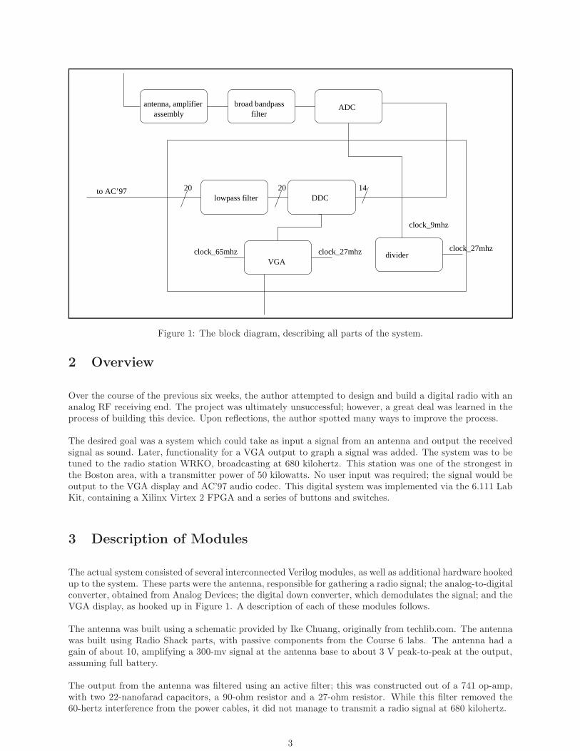
Figure 1: The block diagram, describing all parts of the system.
2 Overview
Over the course of the previous six weeks, the author attempted to design and build a digital radio with ananalog RF receiving end. The project was ultimately unsuccessful; however, a great deal was learned in theprocess of building this device. Upon reflections, the author spotted many ways to improve the process.
The desired goal was a system which could take as input a signal from an antenna and output the receivedsignal as sound. Later, functionality for a VGA output to graph a signal was added. The system was to betuned to the radio station WRKO, broadcasting at 680 kilohertz. This station was one of the strongest inthe Boston area, with a transmitter power of 50 kilowatts. No user input was required; the signal would beoutput to the VGA display and AC’97 audio codec. This digital system was implemented via the 6.111 LabKit, containing a Xilinx Virtex 2 FPGA and a series of buttons and switches.
3 Description of Modules
The actual system consisted of several interconnected Verilog modules, as well as additional hardware hookedup to the system. These parts were the antenna, responsible for gathering a radio signal; the analog-to-digitalconverter, obtained from Analog Devices; the digital down converter, which demodulates the signal; and theVGA display, as hooked up in Figure 1. A description of each of these modules follows.
The antenna was built using a schematic provided by Ike Chuang, originally from techlib.com. The antennawas built using Radio Shack parts, with passive components from the Course 6 labs. The antenna had again of about 10, amplifying a 300-mv signal at the antenna base to about 3 V peak-to-peak at the output,assuming full battery.
The output from the antenna was filtered using an active filter; this was constructed out of a 741 op-amp,with two 22-nanofarad capacitors, a 90-ohm resistor and a 27-ohm resistor. While this filter removed the60-hertz interference from the power cables, it did not manage to transmit a radio signal at 680 kilohertz.
3

The analog to digital converter used was the Analog Devices 9240 evaluation board, part number 9240EB.The ADC had 14 bits of resolution and an adjustable reference voltage, which was set appropriately low.The ADC was capable of sampling at a maximum rate of 10 megahertz, which was sufficient; the minimumsampling rate to recover the entire AM band was 3.4 megahertz. The original 9 megahertz clock provedto be too high a sampling rate, as samples were being dropped at the digital down converter; the authorwas testing clocking the ADC at 1.5 megahertz (extracting samples every 18 cycles); however, tests wereinconclusive.
The digital downconverter was a built-in Xilinx module, which was implemented using the Xilinx CoreGentool. As it included a lowpass filter, the use of this module could have simplified the demodulation processgreatly. However, the author found out that he was specifying the outputs incorrectly, which was a factorin causing the signal to display incorrectly. This will be described in further detail below.
The VGA module was integrated on suggestion of Jae Lee; the goal was to display an arbitrary signal on thescreen. This was largely taken from Ike Chuang’s VGA display module, with some modifications to integrateit into the radio system.
4 Testing and Debugging
The author learned firsthand that redesign of a system is expensive and often painful in terms of time andcomponents. Over the course of this project, the author redesigned the system and revised many of hisinitial assumptions, many of which proved to be wrong.
The first redesign involved rethinking the signal theory in demodulating the signal. Originally, the plan wasto use Fourier transforms to bring the signal into the frequency domain, then use hardware multipliers tofilter and demodulate. However, after discussion, it was determined that doing this was much more complexthan necessary, and it would suffice to multiply the incoming signal by a sine wave and pass the resultingsignal through a lowpass filter to demodulate; the resultant wave would be passed to the audio codec.
The second redesign involved adding a VGA module on recommendation, to visualize the output. Thiswould help debug the signal as it traveled through the system. This VGA module would be connected tothe inputs of various other modules and graph the output.
Unfortunately, rethinking the project meant that much of the previous work done was invalidated dueto incorrect inital assumptions. The author assumed that fast fourier transforms in hardware were fast;instead, compared to the rest of the system, they were much slower than multipliers. While doing manyof the calculations in frequency space would have simplified the problem, it would introduce other designconsiderations–decreasing the sample rate of the ADC to compensate for the delay time and registering theoutputs would be some of the issues raised. Thus, the decision was made to do all calculations in the timedomain.
Interfacing the analog to digital converter to the lab kit was, surprisingly, the most straightforward partof the system. The fact that the Analog Devices ADC took a standard IDE cable spacing was immensleyhelpful; it was not difficult to refer to the Analog Devices schematic and determine the pinout diagram forthe IDE cable. After some initial difficulty with the IDE plugs, the cable slotted smoothly into the board.The protocol written to feed a clock signal into the ADC worked on the first try; as the input clock was setto a multiple of 27 megahertz, the inputs would arrive after an integer number of clock cycles. Connectingthe ADC input to the signal analyzer confirmed that the signal received was the test sine wave.
More testing was made possible with a more complex signal generator; modulated signals could be fed intothe system and the output could be visualized on the VGA display. These signals were correct.
The next most straightforward part of the system to test were the outputs. While there was difficultyintegrating both video and sound, there were preexisting test beds for both; furthermore, the author had
4
done previous work in both sound and video in labs 3 and 4 respectively Thus, after some creativity, it wasnot too difficult to build a system capable of displaying arbitrary video and sound.
The Xilinx modules were poorly documented, which made them difficult to integrate into the rest of thesystem. It was necessary to consult outside references in order to understand the sometimes erratic behaviorof each individual module. The author conducted rudimentary tests on these modules, but after confirmingthey behaved according to their specifications they were mostly left alone.
The antenna was by far the most difficult and frustrating module to debug. While testing outside of the labproduced a reasonable signal; testing with a signal generator produced a small (1.5 to 2 V) but measurablewaveform at the appropriate frequency. By setting the reference voltage of the analog to digital converterat 1 volt, and boosting the gain of the signal using an op-amp, it would be possible to feed that signal intothe labkit.
However, in lab, the presence of several dozen power cables, with 120 volts AC at 15 amperes, made theantenna essentially unusable. Despite attempts to detect a signal by extending the length of the antennawire (at last count, to about six feet) was still insufficient. Filtering did not solve the problem; buildinga bandpass filter and passing the signal through removed the 60 Hz signal; however, the author was toldrecently that an op-amp filter would not pass frequencies in the kilohertz range well and that a tuned LCcircuit was really the only way to solve the problem effectively.
Testing the lowpass filter was done mostly in Matlab, as it was difficult to link a signal generator and outputthe signal. Coefficients for a sine wave were generated in Matlab; an FFT of that wave was taken andmultiplied by the FFT of the filter. The inverse FFT was then taken; while the gain varied, due to roundingissues, the returned signal was correct.
In summary, the VGA modules, sound and ADC worked as described; as their output was visible, it waseasy to see problems with these systems. The Xilinx modules were not functional, nor were some of thehardware components.
5 Conclusion
The author was told that “real companies try building software radios and fail”. While disheartening, thiswas both true and appropriate. The project as initially devised was simply too complex; even the simplifiedsystem was not was too complex to complete. While the author did learn a great deal about design, a purelydigital project would have been much easier to implement. Much time was spent debugging the hardwareand hooking all the pieces of the hardware together; in a purely digital project, this time could have beenspent doing actual design.
While many individual parts of the system functioned, linking them together became increasingly difficultas the complexity increased. Attempting to build a VGA module was a mistake, as it took time away fromdeveloping the core functionality of the system. The author spent too much time attempting to get this towork and not enough time on the audio portion of the system.
The author regrets embarking on this project alone. Making incorrect assumptions about the system sloweddown the project greatly; having someone else versed in the theory would have made the work easier to checkfor sanity. The author has also learned that he does not have the appropriate engineering common senseto immediately see elegant solutions; being able to produce a good solution will require time and multiplerevisions. Starting with correct assumptions helps this problem.
The author also regrets embarking on an ambitious project to link digital and analog parts. A simpler digitalproject would have been easier to complete, without the mess and fuss of hardware interference. The author,however, did learn how to solder properly, which will in the future be useful.
5

5.1 Acknowledgements
Jennifer Novosad for sanity checks of filter design and manuals; Eric Jonas, for sanity checks of filter design,hardware assistance, batteries and manuals; Jae Lee, for assistance with design; Ike Chuang, for schematicsand critique; Dheera Venkatraman, for hardware assistance
6

6 Appendix
Below is the specific Verilog code for this project.
///////////////////////////////////////////////////////////////////////////////
//
// bi-directional monaural interface to AC97
//
///////////////////////////////////////////////////////////////////////////////
module audio (clock_27mhz, reset, audio_in_data, audio_out_data, ready,
audio_reset_b, ac97_sdata_out, ac97_sdata_in,
ac97_synch, ac97_bit_clock);
input clock_27mhz;
input reset;
output [7:0] audio_in_data;
input [7:0] audio_out_data;
output ready;
//ac97 interface signals
output audio_reset_b;
output ac97_sdata_out;
input ac97_sdata_in;
output ac97_synch;
input ac97_bit_clock;
wire [4:0] volume;
wire source;
assign volume = 4’d44; //a reasonable volume value
assign source = 1; //mic
wire [7:0] command_address;
wire [15:0] command_data;
wire command_valid;
wire [19:0] left_in_data, right_in_data;
wire [19:0] left_out_data, right_out_data;
reg audio_reset_b;
reg [9:0] reset_count;
//wait a little before enabling the AC97 codec
always @(posedge clock_27mhz) begin
if (reset) begin
audio_reset_b = 1’b0;
reset_count = 0;
end else if (reset_count == 1023)
audio_reset_b = 1’b1;
else
reset_count = reset_count+1;
end
ac97 ac97(ready, command_address, command_data, command_valid,
left_out_data, 1’b1, right_out_data, 1’b1, left_in_data,
right_in_data, ac97_sdata_out, ac97_sdata_in, ac97_synch,
ac97_bit_clock);
7

ac97commands cmds(clock_27mhz, ready, command_address, command_data,
command_valid, volume, source);
assign left_out_data = {audio_out_data, 12’b000000000000};
assign right_out_data = left_out_data;
//arbitrarily choose left input, get highest-order bits
assign audio_in_data = left_in_data[19:12];
endmodule
// assemble/disassemble AC97 serial frames
module ac97 (ready,
command_address, command_data, command_valid,
left_data, left_valid,
right_data, right_valid,
left_in_data, right_in_data,
ac97_sdata_out, ac97_sdata_in, ac97_synch, ac97_bit_clock);
output ready;
input [7:0] command_address;
input [15:0] command_data;
input command_valid;
input [19:0] left_data, right_data;
input left_valid, right_valid;
output [19:0] left_in_data, right_in_data;
input ac97_sdata_in;
input ac97_bit_clock;
output ac97_sdata_out;
output ac97_synch;
reg ready;
reg ac97_sdata_out;
reg ac97_synch;
reg [7:0] bit_count;
reg [19:0] l_cmd_addr;
reg [19:0] l_cmd_data;
reg [19:0] l_left_data, l_right_data;
reg l_cmd_v, l_left_v, l_right_v;
reg [19:0] left_in_data, right_in_data;
initial begin
ready <= 1’b0;
// synthesis attribute init of ready is "0";
ac97_sdata_out <= 1’b0;
// synthesis attribute init of ac97_sdata_out is "0";
ac97_synch <= 1’b0;
// synthesis attribute init of ac97_synch is "0";
bit_count <= 8’h00;
// synthesis attribute init of bit_count is "0000";
8

l_cmd_v <= 1’b0;
// synthesis attribute init of l_cmd_v is "0";
l_left_v <= 1’b0;
// synthesis attribute init of l_left_v is "0";
l_right_v <= 1’b0;
// synthesis attribute init of l_right_v is "0";
left_in_data <= 20’h00000;
// synthesis attribute init of left_in_data is "00000";
right_in_data <= 20’h00000;
// synthesis attribute init of right_in_data is "00000";
end
always @(posedge ac97_bit_clock) begin
// Generate the sync signal
if (bit_count == 255)
ac97_synch <= 1’b1;
if (bit_count == 15)
ac97_synch <= 1’b0;
// Generate the ready signal
if (bit_count == 128)
ready <= 1’b1;
if (bit_count == 2)
ready <= 1’b0;
// Latch user data at the end of each frame. This ensures that the
// first frame after reset will be empty.
if (bit_count == 255)
begin
l_cmd_addr <= {command_address, 12’h000};
l_cmd_data <= {command_data, 4’h0};
l_cmd_v <= command_valid;
l_left_data <= left_data;
l_left_v <= left_valid;
l_right_data <= right_data;
l_right_v <= right_valid;
end
if ((bit_count >= 0) && (bit_count <= 15))
// Slot 0: Tags
case (bit_count[3:0])
4’h0: ac97_sdata_out <= 1’b1; // Frame valid
4’h1: ac97_sdata_out <= l_cmd_v; // Command address valid
4’h2: ac97_sdata_out <= l_cmd_v; // Command data valid
4’h3: ac97_sdata_out <= l_left_v; // Left data valid
4’h4: ac97_sdata_out <= l_right_v; // Right data valid
default: ac97_sdata_out <= 1’b0;
endcase
else if ((bit_count >= 16) && (bit_count <= 35))
// Slot 1: Command address (8-bits, left justified)
ac97_sdata_out <= l_cmd_v ? l_cmd_addr[35-bit_count] : 1’b0;
else if ((bit_count >= 36) && (bit_count <= 55))
// Slot 2: Command data (16-bits, left justified)
ac97_sdata_out <= l_cmd_v ? l_cmd_data[55-bit_count] : 1’b0;
9

else if ((bit_count >= 56) && (bit_count <= 75))
begin
// Slot 3: Left channel
ac97_sdata_out <= l_left_v ? l_left_data[19] : 1’b0;
l_left_data <= { l_left_data[18:0], l_left_data[19] };
end
else if ((bit_count >= 76) && (bit_count <= 95))
// Slot 4: Right channel
ac97_sdata_out <= l_right_v ? l_right_data[95-bit_count] : 1’b0;
else
ac97_sdata_out <= 1’b0;
bit_count <= bit_count+1;
end // always @ (posedge ac97_bit_clock)
always @(negedge ac97_bit_clock) begin
if ((bit_count >= 57) && (bit_count <= 76))
// Slot 3: Left channel
left_in_data <= { left_in_data[18:0], ac97_sdata_in };
else if ((bit_count >= 77) && (bit_count <= 96))
// Slot 4: Right channel
right_in_data <= { right_in_data[18:0], ac97_sdata_in };
end
endmodule
// issue initialization commands to AC97
module ac97commands (clock, ready, command_address, command_data,
command_valid, volume, source);
input clock;
input ready;
output [7:0] command_address;
output [15:0] command_data;
output command_valid;
input [4:0] volume;
input source;
reg [23:0] command;
reg command_valid;
reg old_ready;
reg done;
reg [3:0] state;
initial begin
command <= 4’h0;
// synthesis attribute init of command is "0";
command_valid <= 1’b0;
// synthesis attribute init of command_valid is "0";
done <= 1’b0;
// synthesis attribute init of done is "0";
old_ready <= 1’b0;
// synthesis attribute init of old_ready is "0";
state <= 16’h0000;
10

// synthesis attribute init of state is "0000";
end
assign command_address = command[23:16];
assign command_data = command[15:0];
wire [4:0] vol;
assign vol = 31-volume;
always @(posedge clock) begin
if (ready && (!old_ready))
state <= state+1;
case (state)
4’h0: // Read ID
begin
command <= 24’h80_0000;
command_valid <= 1’b1;
end
4’h1: // Read ID
command <= 24’h80_0000;
4’h3: // headphone volume
command <= { 8’h04, 3’b000, vol, 3’b000, vol };
4’h5: // PCM volume
command <= 24’h18_0808;
4’h6: // Record source select
command <= 24’h1A_0000; // microphone
4’h7: // Record gain = max
command <= 24’h1C_0F0F;
4’h9: // set +20db mic gain
command <= 24’h0E_8048;
4’hA: // Set beep volume
command <= 24’h0A_0000;
4’hB: // PCM out bypass mix1
command <= 24’h20_8000;
default:
command <= 24’h80_0000;
endcase // case(state)
old_ready <= ready;
end // always @ (posedge clock)
endmodule // ac97commands
///////////////////////////////////////////////////////////////////////////////
//
// Pushbutton Debounce Module (video version)
//
///////////////////////////////////////////////////////////////////////////////
module debounce (reset, clock_65mhz, noisy, clean);
input reset, clock_65mhz, noisy;
output clean;
11

reg [19:0] count;
reg new, clean;
always @(posedge clock_65mhz)
if (reset) begin new <= noisy; clean <= noisy; count <= 0; end
else if (noisy != new) begin new <= noisy; count <= 0; end
else if (count == 650000) clean <= new;
else count <= count+1;
endmodule
///////////////////////////////////////////////////////////////////////////////
//
// tone750mhz Module
//
///////////////////////////////////////////////////////////////////////////////
module tone750hz (clock, ready, pcm_data);
input clock;
input ready;
output [19:0] pcm_data;
reg rdy, old_ready;
reg [8:0] index;
reg [19:0] pcm_data;
initial begin
old_ready <= 1’b0;
// synthesis attribute init of old_ready is "0";
index <= 8’h00;
// synthesis attribute init of index is "00";
pcm_data <= 20’h00000;
// synthesis attribute init of pcm_data is "00000";
end
always @(posedge clock) begin
if (rdy && ~old_ready)
index <= index+1;
old_ready <= rdy;
rdy <= ready;
end
// one cycle of a sinewave in 64 20-bit samples
always @(index) begin
case (index[5:0])
6’h00: pcm_data <= 20’h00000;
6’h01: pcm_data <= 20’h0C8BD;
6’h02: pcm_data <= 20’h18F8B;
6’h03: pcm_data <= 20’h25280;
6’h04: pcm_data <= 20’h30FBC;
6’h05: pcm_data <= 20’h3C56B;
6’h06: pcm_data <= 20’h471CE;
6’h07: pcm_data <= 20’h5133C;
6’h08: pcm_data <= 20’h5A827;
12

6’h09: pcm_data <= 20’h62F20;
6’h0A: pcm_data <= 20’h6A6D9;
6’h0B: pcm_data <= 20’h70E2C;
6’h0C: pcm_data <= 20’h7641A;
6’h0D: pcm_data <= 20’h7A7D0;
6’h0E: pcm_data <= 20’h7D8A5;
6’h0F: pcm_data <= 20’h7F623;
6’h10: pcm_data <= 20’h7FFFF;
6’h11: pcm_data <= 20’h7F623;
6’h12: pcm_data <= 20’h7D8A5;
6’h13: pcm_data <= 20’h7A7D0;
6’h14: pcm_data <= 20’h7641A;
6’h15: pcm_data <= 20’h70E2C;
6’h16: pcm_data <= 20’h6A6D9;
6’h17: pcm_data <= 20’h62F20;
6’h18: pcm_data <= 20’h5A827;
6’h19: pcm_data <= 20’h5133C;
6’h1A: pcm_data <= 20’h471CE;
6’h1B: pcm_data <= 20’h3C56B;
6’h1C: pcm_data <= 20’h30FBC;
6’h1D: pcm_data <= 20’h25280;
6’h1E: pcm_data <= 20’h18F8B;
6’h1F: pcm_data <= 20’h0C8BD;
6’h20: pcm_data <= 20’h00000;
6’h21: pcm_data <= 20’hF3743;
6’h22: pcm_data <= 20’hE7075;
6’h23: pcm_data <= 20’hDAD80;
6’h24: pcm_data <= 20’hCF044;
6’h25: pcm_data <= 20’hC3A95;
6’h26: pcm_data <= 20’hB8E32;
6’h27: pcm_data <= 20’hAECC4;
6’h28: pcm_data <= 20’hA57D9;
6’h29: pcm_data <= 20’h9D0E0;
6’h2A: pcm_data <= 20’h95927;
6’h2B: pcm_data <= 20’h8F1D4;
6’h2C: pcm_data <= 20’h89BE6;
6’h2D: pcm_data <= 20’h85830;
6’h2E: pcm_data <= 20’h8275B;
6’h2F: pcm_data <= 20’h809DD;
6’h30: pcm_data <= 20’h80000;
6’h31: pcm_data <= 20’h809DD;
6’h32: pcm_data <= 20’h8275B;
6’h33: pcm_data <= 20’h85830;
6’h34: pcm_data <= 20’h89BE6;
6’h35: pcm_data <= 20’h8F1D4;
6’h36: pcm_data <= 20’h95927;
6’h37: pcm_data <= 20’h9D0E0;
6’h38: pcm_data <= 20’hA57D9;
6’h39: pcm_data <= 20’hAECC4;
6’h3A: pcm_data <= 20’hB8E32;
6’h3B: pcm_data <= 20’hC3A95;
6’h3C: pcm_data <= 20’hCF044;
6’h3D: pcm_data <= 20’hDAD80;
6’h3E: pcm_data <= 20’hE7075;
6’h3F: pcm_data <= 20’hF3743;
endcase // case(index[5:0])
end // always @ (index)
13

endmodule
///////////////////////////////////////////////////////////////////////////////
//
// 6.111 FPGA Labkit -- Template Toplevel Module
//
// For Labkit Revision 004
//
//
// Created: October 31, 2004, from revision 003 file
// Author: Nathan Ickes
//
///////////////////////////////////////////////////////////////////////////////
//
// CHANGES FOR BOARD REVISION 004
//
// 1) Added signals for logic analyzer pods 2-4.
// 2) Expanded "tv_in_ycrcb" to 20 bits.
// 3) Renamed "tv_out_data" to "tv_out_i2c_data" and "tv_out_sclk" to
// "tv_out_i2c_clock".
// 4) Reversed disp_data_in and disp_data_out signals, so that "out" is an
// output of the FPGA, and "in" is an input.
//
// CHANGES FOR BOARD REVISION 003
//
// 1) Combined flash chip enables into a single signal, flash_ce_b.
//
// CHANGES FOR BOARD REVISION 002
//
// 1) Added SRAM clock feedback path input and output
// 2) Renamed "mousedata" to "mouse_data"
// 3) Renamed some ZBT memory signals. Parity bits are now incorporated into
// the data bus, and the byte write enables have been combined into the
// 4-bit ram#_bwe_b bus.
// 4) Removed the "systemace_clock" net, since the SystemACE clock is now
// hardwired on the PCB to the oscillator.
//
///////////////////////////////////////////////////////////////////////////////
//
// Complete change history (including bug fixes)
//
// 2005-Sep-09: Added missing default assignments to "ac97_sdata_out",
// "disp_data_out", "analyzer[2-3]_clock" and
// "analyzer[2-3]_data".
//
// 2005-Jan-23: Reduced flash address bus to 24 bits, to match 128Mb devices
// actually populated on the boards. (The boards support up to
// 256Mb devices, with 25 address lines.)
//
// 2004-Oct-31: Adapted to new revision 004 board.
//
// 2004-May-01: Changed "disp_data_in" to be an output, and gave it a default
// value. (Previous versions of this file declared this port to
// be an input.)
//
// 2004-Apr-29: Reduced SRAM address busses to 19 bits, to match 18Mb devices
14

// actually populated on the boards. (The boards support up to
// 72Mb devices, with 21 address lines.)
//
// 2004-Apr-29: Change history started
//
///////////////////////////////////////////////////////////////////////////////
module radio (beep, audio_reset_b, ac97_sdata_out, ac97_sdata_in, ac97_synch,
ac97_bit_clock,
vga_out_red, vga_out_green, vga_out_blue, vga_out_sync_b,
vga_out_blank_b, vga_out_pixel_clock, vga_out_hsync,
vga_out_vsync,
tv_out_ycrcb, tv_out_reset_b, tv_out_clock, tv_out_i2c_clock,
tv_out_i2c_data, tv_out_pal_ntsc, tv_out_hsync_b,
tv_out_vsync_b, tv_out_blank_b, tv_out_subcar_reset,
tv_in_ycrcb, tv_in_data_valid, tv_in_line_clock1,
tv_in_line_clock2, tv_in_aef, tv_in_hff, tv_in_aff,
tv_in_i2c_clock, tv_in_i2c_data, tv_in_fifo_read,
tv_in_fifo_clock, tv_in_iso, tv_in_reset_b, tv_in_clock,
ram0_data, ram0_address, ram0_adv_ld, ram0_clk, ram0_cen_b,
ram0_ce_b, ram0_oe_b, ram0_we_b, ram0_bwe_b,
ram1_data, ram1_address, ram1_adv_ld, ram1_clk, ram1_cen_b,
ram1_ce_b, ram1_oe_b, ram1_we_b, ram1_bwe_b,
clock_feedback_out, clock_feedback_in,
flash_data, flash_address, flash_ce_b, flash_oe_b, flash_we_b,
flash_reset_b, flash_sts, flash_byte_b,
rs232_txd, rs232_rxd, rs232_rts, rs232_cts,
mouse_clock, mouse_data, keyboard_clock, keyboard_data,
clock_27mhz, clock1, clock2,
disp_blank, disp_data_out, disp_clock, disp_rs, disp_ce_b,
disp_reset_b, disp_data_in,
button0, button1, button2, button3, button_enter, button_right,
button_left, button_down, button_up,
switch,
led,
user1, user2, user3, user4,
daughtercard,
systemace_data, systemace_address, systemace_ce_b,
15

systemace_we_b, systemace_oe_b, systemace_irq, systemace_mpbrdy,
analyzer1_data, analyzer1_clock,
analyzer2_data, analyzer2_clock,
analyzer3_data, analyzer3_clock,
analyzer4_data, analyzer4_clock);
output beep, audio_reset_b, ac97_synch, ac97_sdata_out;
input ac97_bit_clock, ac97_sdata_in;
output [7:0] vga_out_red, vga_out_green, vga_out_blue;
output vga_out_sync_b, vga_out_blank_b, vga_out_pixel_clock,
vga_out_hsync, vga_out_vsync;
output [9:0] tv_out_ycrcb;
output tv_out_reset_b, tv_out_clock, tv_out_i2c_clock, tv_out_i2c_data,
tv_out_pal_ntsc, tv_out_hsync_b, tv_out_vsync_b, tv_out_blank_b,
tv_out_subcar_reset;
input [19:0] tv_in_ycrcb;
input tv_in_data_valid, tv_in_line_clock1, tv_in_line_clock2, tv_in_aef,
tv_in_hff, tv_in_aff;
output tv_in_i2c_clock, tv_in_fifo_read, tv_in_fifo_clock, tv_in_iso,
tv_in_reset_b, tv_in_clock;
inout tv_in_i2c_data;
inout [35:0] ram0_data;
output [18:0] ram0_address;
output ram0_adv_ld, ram0_clk, ram0_cen_b, ram0_ce_b, ram0_oe_b, ram0_we_b;
output [3:0] ram0_bwe_b;
inout [35:0] ram1_data;
output [18:0] ram1_address;
output ram1_adv_ld, ram1_clk, ram1_cen_b, ram1_ce_b, ram1_oe_b, ram1_we_b;
output [3:0] ram1_bwe_b;
input clock_feedback_in;
output clock_feedback_out;
inout [15:0] flash_data;
output [23:0] flash_address;
output flash_ce_b, flash_oe_b, flash_we_b, flash_reset_b, flash_byte_b;
input flash_sts;
output rs232_txd, rs232_rts;
input rs232_rxd, rs232_cts;
input mouse_clock, mouse_data, keyboard_clock, keyboard_data;
input clock_27mhz, clock1, clock2;
output disp_blank, disp_clock, disp_rs, disp_ce_b, disp_reset_b;
input disp_data_in;
output disp_data_out;
input button0, button1, button2, button3, button_enter, button_right,
button_left, button_down, button_up;
16

input [7:0] switch;
output [7:0] led;
inout [31:0] user1, user2, user3, user4;
inout [43:0] daughtercard;
inout [15:0] systemace_data;
output [6:0] systemace_address;
output systemace_ce_b, systemace_we_b, systemace_oe_b;
input systemace_irq, systemace_mpbrdy;
output [15:0] analyzer1_data, analyzer2_data, analyzer3_data,
analyzer4_data;
output analyzer1_clock, analyzer2_clock, analyzer3_clock, analyzer4_clock;
////////////////////////////////////////////////////////////////////////////
//
// I/O Assignments
//
////////////////////////////////////////////////////////////////////////////
// Video Output
assign tv_out_ycrcb = 10’h0;
assign tv_out_reset_b = 1’b0;
assign tv_out_clock = 1’b0;
assign tv_out_i2c_clock = 1’b0;
assign tv_out_i2c_data = 1’b0;
assign tv_out_pal_ntsc = 1’b0;
assign tv_out_hsync_b = 1’b1;
assign tv_out_vsync_b = 1’b1;
assign tv_out_blank_b = 1’b1;
assign tv_out_subcar_reset = 1’b0;
// Video Input
assign tv_in_i2c_clock = 1’b0;
assign tv_in_fifo_read = 1’b0;
assign tv_in_fifo_clock = 1’b0;
assign tv_in_iso = 1’b0;
assign tv_in_reset_b = 1’b0;
assign tv_in_clock = 1’b0;
assign tv_in_i2c_data = 1’bZ;
// tv_in_ycrcb, tv_in_data_valid, tv_in_line_clock1, tv_in_line_clock2,
// tv_in_aef, tv_in_hff, and tv_in_aff are inputs
// SRAMs
assign ram0_data = 36’hZ;
assign ram0_address = 19’h0;
assign ram0_adv_ld = 1’b0;
assign ram0_clk = 1’b0;
assign ram0_cen_b = 1’b1;
assign ram0_ce_b = 1’b1;
assign ram0_oe_b = 1’b1;
assign ram0_we_b = 1’b1;
assign ram0_bwe_b = 4’hF;
assign ram1_data = 36’hZ;
assign ram1_address = 19’h0;
17

assign ram1_adv_ld = 1’b0;
assign ram1_clk = 1’b0;
assign ram1_cen_b = 1’b1;
assign ram1_ce_b = 1’b1;
assign ram1_oe_b = 1’b1;
assign ram1_we_b = 1’b1;
assign ram1_bwe_b = 4’hF;
assign clock_feedback_out = 1’b0;
// clock_feedback_in is an input
// Flash ROM
assign flash_data = 16’hZ;
assign flash_address = 24’h0;
assign flash_ce_b = 1’b1;
assign flash_oe_b = 1’b1;
assign flash_we_b = 1’b1;
assign flash_reset_b = 1’b0;
assign flash_byte_b = 1’b1;
// flash_sts is an input
// RS-232 Interface
assign rs232_txd = 1’b1;
assign rs232_rts = 1’b1;
// rs232_rxd and rs232_cts are inputs
// PS/2 Ports
// mouse_clock, mouse_data, keyboard_clock, and keyboard_data are inputs
// LED Displays
assign disp_blank = 1’b1;
assign disp_clock = 1’b0;
assign disp_rs = 1’b0;
assign disp_ce_b = 1’b1;
assign disp_reset_b = 1’b0;
assign disp_data_out = 1’b0;
// disp_data_in is an input
// Buttons, Switches, and Individual LEDs
//lab3 assign led = 8’hFF;
// button0, button1, button2, button3, button_enter, button_right,
// button_left, button_down, button_up, and switches are inputs
wire test;
assign test = switch[7];
// Daughtercard Connectors
assign daughtercard = 44’hZ;
// SystemACE Microprocessor Port
assign systemace_data = 16’hZ;
assign systemace_address = 7’h0;
assign systemace_ce_b = 1’b1;
assign systemace_we_b = 1’b1;
assign systemace_oe_b = 1’b1;
// systemace_irq and systemace_mpbrdy are inputs
// Logic Analyzer
18

assign analyzer1_data = adctotal;
assign analyzer1_clock = clock_9mhz;
assign analyzer2_data = 16’h0;
assign analyzer2_clock = 1’b1;
assign analyzer3_data = 16’h0;
assign analyzer3_clock = 1’b1;
assign analyzer4_data = 16’h0;
assign analyzer4_clock = 1’b1;
////////////////////////////////////////////////////////////////////////////
//
// digital radio modules begin here
//
////////////////////////////////////////////////////////////////////////////
//take the ADC input, link to ddc
wire adcinput0;
wire [1:0] adcinput2;
wire [10:0] adcinput3;
wire [13:0] adctotal;
assign adcinput1 = user1[3];
assign adcinput2 = user1[7:6];
assign adcinput3 = user1[19:9];
assign adctotal = {adcinput3, adcinput2, adcinput1};
adcclock adclock(clock_27mhz, clock_9mhz);
assign user2[0] = clock_9mhz;
assign user4[31] = clock_9mhz;
assign user3[13:0] = adctotal;
// use FPGA’s digital clock manager to produce a
// 65MHz clock (actually 64.8MHz)
wire clock_65mhz_unbuf,clock_65mhz;
DCM vclk1(.CLKIN(clock_27mhz),.CLKFX(clock_65mhz_unbuf));
// synthesis attribute CLKFX_DIVIDE of vclk1 is 10
// synthesis attribute CLKFX_MULTIPLY of vclk1 is 24
// synthesis attribute CLK_FEEDBACK of vclk1 is NONE
// synthesis attribute CLKIN_PERIOD of vclk1 is 37
BUFG vclk2(.O(clock_65mhz),.I(clock_65mhz_unbuf));
// power-on reset generation
wire power_on_reset; // remain high for first 16 clocks
SRL16 reset_sr (.D(1’b0), .CLK(clock_65mhz), .Q(power_on_reset),
.A0(1’b1), .A1(1’b1), .A2(1’b1), .A3(1’b1));
defparam reset_sr.INIT = 16’hFFFF;
// ENTER button is user reset
wire reset,user_reset;
debounce db1(power_on_reset, clock_65mhz, ~button_enter, user_reset);
assign reset = user_reset | power_on_reset;
19

// UP and DOWN buttons
wire up,down;
debounce db2(reset, clock_65mhz, ~button_up, up);
debounce db3(reset, clock_65mhz, ~button_down, down);
// generate basic XVGA video signals
wire [10:0] hcount;
wire [9:0] vcount;
wire hsync,vsync,blank;
xvga xvga1(clock_65mhz,hcount,vcount,hsync,vsync,blank);
// feed XVGA signals to user’s pong game
wire [2:0] pixel;
wire phsync,pvsync,pblank;
wire pix_clk;
assign pix_clk = vga_out_pixel_clock;
//////
// AC97 output.
//////
wire [7:0] from_ac97_data, to_ac97_data;
wire audio_ready;
// AC97 driver
audio a(clock_27mhz, reset, from_ac97_data, to_ac97_data, audio_ready,
audio_reset_b, ac97_sdata_out, ac97_sdata_in,
ac97_synch, ac97_bit_clock);
vga_main vgamain(clock_27mhz, clock_65mhz, reset,pix_clk,up,down,
hcount,vcount,hsync,vsync,blank,adctotal, dout,
phsync,pvsync,pblank,pixel,audio_ready,from_ac97_data, to_ac97_data, test);
// switch[1:0] selects which video generator to use:
// 00: VGA output
// 01: 1 pixel outline of active video area (adjust screen controls)
// 10: color bars
reg [2:0] rgb;
reg b,hs,vs;
always @(posedge clock_65mhz) begin
if (switch[1:0] == 2’b01) begin
// 1 pixel outline of visible area (white)
hs <= hsync;
vs <= vsync;
b <= blank;
rgb <= (hcount==0 | hcount==1023 | vcount==0 | vcount==767) ? 7 : 0;
end else if (switch[1:0] == 2’b10) begin
// color bars
hs <= hsync;
vs <= vsync;
b <= blank;
rgb <= hcount[8:6];
end else begin
// default: radio
hs <= phsync;
20

vs <= pvsync;
b <= pblank;
rgb <= pixel;
end
end
// VGA Output. In order to meet the setup and hold times of the
// AD7125, we send it ~clock_65mhz.
assign vga_out_red = {8{rgb[2]}};
assign vga_out_green = {8{rgb[1]}};
assign vga_out_blue = {8{rgb[0]}};
assign vga_out_sync_b = 1’b1; // not used
assign vga_out_blank_b = ~b;
assign vga_out_pixel_clock = ~clock_65mhz;
assign vga_out_hsync = hs;
assign vga_out_vsync = vs;
// downconverter
wire [13:0] DIN;
wire ND, CLK;
assign DIN = adctotal; //data in comes from user4 channel
assign ND = clock_9mhz; //new samples ready every 3 cycles
assign CLK = clock_27mhz; // clock off system clock
ddc downconverter(DIN,
ND,
CLK,
rdy,
rfd,
dout_i,
dout_q
);
//wire [19:0] dout;
assign dout = (dout_i * dout_i) + (dout_q * dout_q); //calculate magnitude of output signal
assign user4[19:0] = dout;
endmodule
////////////////////////////////////////////////////////////////////////////////
//
// xvga: Generate XVGA display signals (1024 x 768 @ 60Hz)
//
////////////////////////////////////////////////////////////////////////////////
module xvga(vclock,hcount,vcount,hsync,vsync,blank);
input vclock;
output [10:0] hcount;
output [9:0] vcount;
output vsync;
output hsync;
output blank;
reg hsync,vsync,hblank,vblank,blank;
reg [10:0] hcount; // pixel number on current line
21

reg [9:0] vcount; // line number
// horizontal: 1344 pixels total
// display 1024 pixels per line
wire hsyncon,hsyncoff,hreset,hblankon;
assign hblankon = (hcount == 1023);
assign hsyncon = (hcount == 1047);
assign hsyncoff = (hcount == 1183);
assign hreset = (hcount == 1343);
// vertical: 806 lines total
// display 768 lines
wire vsyncon,vsyncoff,vreset,vblankon;
assign vblankon = hreset & (vcount == 767);
assign vsyncon = hreset & (vcount == 776);
assign vsyncoff = hreset & (vcount == 782);
assign vreset = hreset & (vcount == 805);
// sync and blanking
wire next_hblank,next_vblank;
assign next_hblank = hreset ? 0 : hblankon ? 1 : hblank;
assign next_vblank = vreset ? 0 : vblankon ? 1 : vblank;
always @(posedge vclock) begin
hcount <= hreset ? 0 : hcount + 1;
hblank <= next_hblank;
hsync <= hsyncon ? 0 : hsyncoff ? 1 : hsync; // active low
vcount <= hreset ? (vreset ? 0 : vcount + 1) : vcount;
vblank <= next_vblank;
vsync <= vsyncon ? 0 : vsyncoff ? 1 : vsync; // active low
blank <= next_vblank | (next_hblank & ~hreset);
end
endmodule
////////////////////////////////////////////////////////////////////////////////
//
// vga_main: the vga display tool
//
////////////////////////////////////////////////////////////////////////////////
module vga_main (toneclk, vclock, reset,pix_clk,up,down,
hcount,vcount,hsync,vsync,blank,data1,data2,
phsync,pvsync,pblank,pixel,audio_ready,from_ac97_data, to_ac97_data, switch);
input vclock; // 65MHz clock
input toneclk;
input reset; // 1 to initialize module
input up; // 1 to control tuner input
input down; // 1 to control tuner input
input [10:0] hcount; // horizontal index of current pixel (0..1023)
input [9:0] vcount; // vertical index of current pixel (0..767)
input hsync; // XVGA horizontal sync signal (active low)
input vsync; // XVGA vertical sync signal (active low)
input blank; // XVGA blanking (1 means output black pixel)
input pix_clk;
22

input audio_ready;
input [7:0] from_ac97_data;
input signed [19:0] data1, data2;
input switch;
output [7:0] to_ac97_data;
output phsync;
output pvsync;
output pblank;
output [2:0] pixel;
wire [19:0] pcm_data;
wire [2:0] pix_test;
reg ready;
reg [5:0] counter;
reg [15:0] square;
// test--generates a square wave at 27mhz
always @ (posedge toneclk)
begin
case (counter)
15:
begin
counter <= counter + 1;
square <= 31;
ready <= 1;
end
16:
begin
counter <= counter + 1;
ready <= 0;
end
31:
begin
counter <= 0;
square <= 16;
end
default:
begin
counter <= counter + 1;
square <= square;
end
endcase
end
reg [20:0] gain;
always @ (posedge toneclk)
gain <= 32 * data2;
vga_graph2_buf graph(vclock, reset, pix_clk, hcount, vcount, pix_test,
to_ac97_data, gain[7:0]+100, toneclk, ready, 200, 200);
assign phsync = hsync;
assign pvsync = vsync;
23

assign pblank = blank;
assign pixel = pix_test;
// detect clock cycle when READY goes 0 -> 1
// f(READY) = 48khz
wire new_frame;
reg old_ready;
always @ (posedge toneclk) old_ready <= reset ? 0 : ready;
assign new_frame = audio_ready & ~old_ready;
wire [19:0] tone;
tone750hz xxx(toneclk, audio_ready, pcm_data);
reg [7:0] to_ac97_data;
always @ (posedge toneclk) begin
if (new_frame) begin
// just received new data from the AC97
to_ac97_data <= switch? pcm_data[19:12] : gain[7:0];
end
end
endmodule
module vga_graph2_buf (vclock,reset,pix_clk,hcount,vcount,pixel,
data1,data2,dclk,dstart,cx,cy);
parameter NX = 640; // number of data pixels (horiz size)
parameter GPIX_RGB1 = 3’b111; // pixel RGB for graph data1
parameter GPIX_RGB2 = 3’b100; // pixel RGB for graph data2
input reset; // system reset
input vclock; // system synchronous clock
input pix_clk; // video pixel clock
input [9:0] hcount; // horizontal index of current pixel (0..639)
input [9:0] vcount; // vertical index of current pixel (0..479)
output [2:0] pixel; // char display’s pixel
input [9:0] cx; // x-location of graph (upper left corner)
input [9:0] cy; // y-location of graph (upper left corner)
input [7:0] data1; // next data word to clock in
input [7:0] data2; // next data word to clock in
input dclk; // data clock
input dstart; // pulse to start data input
// data is loaded begining with the clock cycle after (the single-cycle)
// dstart signal rises.
reg [7:0] gdat1[NX:0]; // ring buffer memory for display data1
reg [7:0] gdat2[NX:0]; // ring buffer memory for display data2
// pixels for the graph
wire [9:0] hoff = hcount-cx;
reg [9:0] hptr;
always @(posedge vclock)
hptr <= (hoff==0) ? 11’b0 // start display pointer at zero
: ~pix_clk ? hptr
: (hptr == NX-1 ? 0 : hptr+1);
24

wire [9:0] voff = vcount - cy;
wire [2:0] gpix = ( ((voff==gdat1[hptr]) ? GPIX_RGB1 : 3’b0)
| ((voff==gdat2[hptr]) ? GPIX_RGB2 : 3’b0) );
// clocking in new data
reg [7:0] vdat1[NX:0]; // ring buffer memory for incoming data1
reg [7:0] vdat2[NX:0]; // ring buffer memory for incoming data2
reg [10:0] buf_cnt; // counter on current size of new sample buf
reg [10:0] cp_cnt; // count of samples copied to display buffer
reg loading;
reg [1:0] view_cycle; // number of vid frames after copy_done raised
wire end_buf = (buf_cnt==NX);
wire frame_over = (vcount == 478) & (hcount == 1) & pix_clk;
wire copy_flag = loading & end_buf; // copy requested
wire view_done = (view_cycle==2); // new data displayed
wire copy_done = (cp_cnt == NX) ? 1 : 0; // copy done
wire new_set = copy_done & view_done; // req new set of data
// loop which makes sure a full video frame is displayed after
// loaded data is copied to display buffer, before new sample is taken
always @(posedge vclock)
view_cycle <= (reset | ~copy_done) ? 0
: (copy_done & frame_over) ? view_cycle + 1
: view_cycle;
// main loop which samples data and checks for load request
always @(posedge vclock)
if (reset)
begin
buf_cnt <= 0;
loading <= 0;
end
else if (dclk) // dclk is the clock-enable data clock
begin
loading <= new_set ? 0
: dstart ? 1 // start one cycle after dstart rises
: loading;
buf_cnt <= new_set ? 0
: (loading & ~end_buf) ? buf_cnt + 1
: buf_cnt;
if (loading)
begin
vdat1[buf_cnt] <= 8’d255 - data1; // store data
vdat2[buf_cnt] <= 8’d255 - data2; // store data
end
end
// copy from input buffer to display buffer when loaded & inbuf full
always @(posedge vclock)
begin
// cp_cnt counts up to NX-1 and stays there until copy_flag -> 0
25

cp_cnt <= copy_flag ? ((cp_cnt < NX) ? cp_cnt + 1 : cp_cnt) : 0;
gdat1[cp_cnt] <= copy_flag ? vdat1[cp_cnt] : gdat1[cp_cnt];
gdat2[cp_cnt] <= copy_flag ? vdat2[cp_cnt] : gdat2[cp_cnt];
end
// border
wire bpixfl = (hoff==0) | (hoff==NX) | (voff==0) | (voff==254);
wire [2:0] bpix = bpixfl ? 3’b010 : 3’b0;
// display flag
wire dispflag = ( (hcount>=cx) & (hcount <= cx+NX) & (vcount >= cy-1) &
(vcount <= (cy+10’d254)) );
// final pixel output
reg [2:0] pixel;
always @(posedge vclock)
pixel <= pix_clk ? (dispflag ? gpix | bpix : 0) : pixel;
endmodule // vga_graph
module adcclock(clk_27mhz, clk_9mhz);
input clk_27mhz;
output clk_9mhz;
reg clk_9mhz = 1;
reg [2:0] counter = 20;
always @ (posedge clk_27mhz)
begin
case (counter)
20: begin
counter <= 0;
clk_9mhz <= ~clk_9mhz;
end
default
counter <= counter + 1;
endcase // case(counter)
end // always @ (posedge clk_27mhz)
endmodule // adcclock
26