Radiation Effects Assessment of MRAM Devices Elghefari...National Aeronautics and Space...
18
National Aeronautics and Space Administration Radiation Effects Assessment of MRAM Devices Mohamed Elghefari Jet Propulsion Laboratory Pasadena, California Steve McClure Jet Propulsion Laboratory Pasadena, California Jet Propulsion Laboratory California Institute of Technology Pasadena, California JPL Publication 08-19 5/08
Transcript of Radiation Effects Assessment of MRAM Devices Elghefari...National Aeronautics and Space...

National Aeronautics and Space Administration
Radiation Effects Assessment of MRAM Devices
Mohamed Elghefari Jet Propulsion Laboratory
Pasadena, California
Steve McClure Jet Propulsion Laboratory
Pasadena, California
Jet Propulsion Laboratory California Institute of Technology
Pasadena, California
JPL Publication 08-19 5/08


National Aeronautics and Space Administration
Radiation Effects Assessment of MRAM Devices
NASA Electronic Parts and Packaging (NEPP) Program
Office of Safety and Mission Assurance
Mohamed Elghefari Jet Propulsion Laboratory
Pasadena, California
Steve McClure Jet Propulsion Laboratory
Pasadena, California
NASA WBS: 939904.01.11.30 JPL Project Number: 102197
Task Number: 3.32.7
Jet Propulsion Laboratory
4800 Oak Grove Drive Pasadena, CA 91109
http://nepp.nasa.gov

ii
This research was carried out at the Jet Propulsion Laboratory, California Institute of
Technology, and was sponsored by the National Aeronautics and Space Administration
Electronic Parts and Packaging (NEPP) Program.
Reference herein to any specific commercial product, process, or service by trade name,
trademark, manufacturer, or otherwise, does not constitute or imply its endorsement by the
United States Government or the Jet Propulsion Laboratory, California Institute of Technology.
Copyright 2008. California Institute of Technology. Government sponsorship acknowledged.

1
RADIATION EFFECTS ASSESSMENT OF MRAM DEVICES
Mohamed Elghefari
Steve McClure
NEPP Program Office of Safety & Mission Assurance
WBS 939904.01.11.30 under TASK ORDER NMO7-10824 Project Number: 102197
Task Number: 3.32.7
Abstract—The Magneto-resistive Random Access Memory (MRAM) from Freescale Semiconductor, MR2A16A, was subjected to heavy ion single event testing. Test results show that this device is sensitive to Single Event Latchup (SEL). The sensitivity of the MRAM was attributed to the complementary metal oxide semiconductor (CMOS) process in which the active portion of this device is constructed. Therefore, the device must be used with caution and may require mitigation techniques if used in a space environment. There was no indication that the MRAM technology itself, the memory element construction, is subject to damage from heavy ions.

2
Table of Contents 1 SCOPE ...................................................................................................................................... 3 2 OBJECTIVES........................................................................................................................... 3 3 INTRODUCTION .................................................................................................................... 3 4 EXPERIMENTAL PROCEDURE ........................................................................................... 5
4.1 The Test Device .............................................................................................................. 5 4.2 Device Preparation.......................................................................................................... 5 4.3 Special Conditions and Ion Range.................................................................................. 7 4.4 Test Facility and Ion Beams Description........................................................................ 8 4.5 SEL Monitoring Capability and Test Circuit.................................................................. 9 4.6 Pre-Test Procedures ...................................................................................................... 10 4.7 Test Details ................................................................................................................... 10
5 ANALYSIS AND RESULTS................................................................................................. 11 6 CONCLUSION....................................................................................................................... 13 REFERENCES ............................................................................................................................. 13

3
1 SCOPEThe Magneto-resistive Random Access Memory (MRAM) is a nonvolatile memory technology that has useful properties for space applications. This Single Event Effects (SEE) evaluation of the MRAM was performed to assess viability for use in NASA missions.
2 OBJECTIVES The purpose of this evaluation is to determine Single Event Latchup (SEL) susceptibility of the 4Mb MR2A16A MRAM from Freescale Semiconductor. The MR2A16A was the only MRAM device available in commercial production at the time of evaluation. The test objectives were as follows:
� Measure the SEL cross section (�) versus Linear Energy Transfer (LET)
� Determine if SEL susceptibility of the device is temperature-dependent
� Perform follow-on functionality checks after each irradiation run
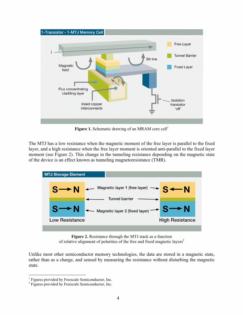
3 INTRODUCTION MRAM technology has the attributes of non-volatility and high speed operation, a combination not found in any other existing non-volatile memory technology. It protects data in the event of power loss and does not require periodic refreshing. MRAM technology also has unlimited read and write endurance, and fast read and write access times; and is protected from inadvertent writes. MRAM is based on magnetic tunnel junction (MTJ) devices integrated with complementary metal oxide semiconductors (CMOS). The MTJ is composed of a fixed ferromagnetic layer, a thin dielectric tunnel barrier, and a free ferromagnetic layer (see Figure 1). A small bias voltage applied to the MTJ causes electrons to tunnel through the dielectric barrier, from one magnetic layer to the other. The tunneling current is spin polarized due to the nature of the conduction bands in the ferromagnetic materials, resulting in more or fewer available states for tunneling depending on the relative polarization of the ferromagnetic layers [1].
4
Figure 1. Schematic drawing of an MRAM core cell1
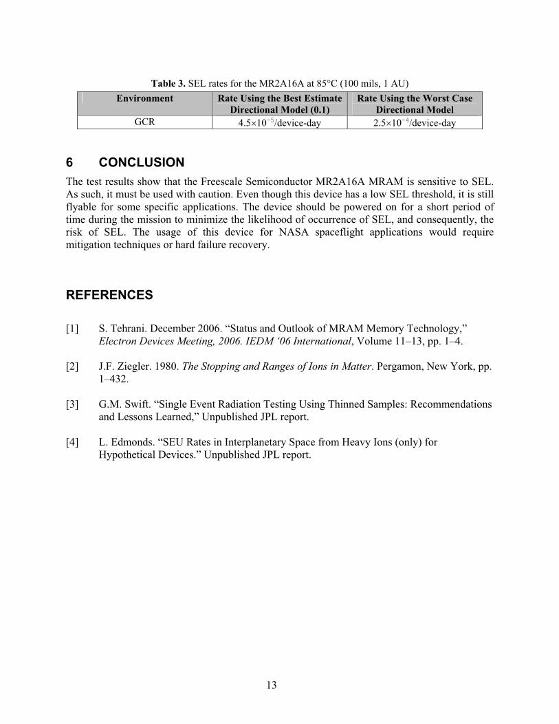
The MTJ has a low resistance when the magnetic moment of the free layer is parallel to the fixed layer, and a high resistance when the free layer moment is oriented anti-parallel to the fixed layer moment (see Figure 2). This change in the tunneling resistance depending on the magnetic state of the device is an effect known as tunneling magnetoresistance (TMR).
Figure 2. Resistance through the MTJ stack as a function
of relative alignment of polarities of the free and fixed magnetic layers2
Unlike most other semiconductor memory technologies, the data are stored in a magnetic state, rather than as a charge, and sensed by measuring the resistance without disturbing the magnetic state.
1 Figures provided by Freescale Semiconductor, Inc. 2 Figures provided by Freescale Semiconductor, Inc.

5
4 EXPERIMENTAL PROCEDURE
4.1 The Test Device The 4Mb MR2A16A MRAM device (Figure 3) is fabricated using the 0.18-μm process technology and runs on an industry-standard 3.3-V center power supply. It has a standard static-random-access-memory (SRAM) pinout, and is organized as 256 Kwords by 16 bits. The device is sealed in a 400-mil, 44-lead thin small outline package (TSOP). Active read and write current values are 55 mA and 105 mA, and typical standby current is 9 mA. Since the device is nonvolatile, it can be turned off completely when not in use.
Figure 3. Freescale Semiconductor's MR2A16A MRAM3
4.2 Device Preparation Before SEL testing could be conducted on the MRAM, a material analysis of the device was performed to determine the best test approach. Scanning Electron Microscopy The scanning electron microscopy (SEM) examination was performed to determine the best heavy ion irradiation approach. The SEM evaluation was carried out using a Hitachi field emission SEM to determine the elemental composition of the magnetic metal shield on the surface of the die and on the metal layer in the back end of the device. Magnifications ranged from 100X to 25,000X.
3 Figures provided by Freescale Semiconductor, Inc.

6
SEM was used in the X-ray energy dispersive spectroscopy (EDS) configuration. The SEM was configured such that the contrast of the image was a map of one or more of the atomic elements present in the sample. Qualitative and quantitative elemental analyses of selected areas of the cross section of the device were performed. The die of one of the devices was first cross-sectioned (Figure 4). An EDS X-ray chemical element line profile was then performed. The top metal layer is approximately 170 microns thick, composed of Mo (50.54%), Ni (36.92%), Fe (15.25%), and Mn (0.78%). Figure 4 shows the MTJ bits integrated with underlying 0.18-�m CMOS circuitry; the Si layer is ~260 �m thick and the Cu layer is 110 �m thick.
Figure 4. Cross section of the die of MR2A16A MRAM Chemical Etching All devices must be without lids to permit access of the heavy ion beam to the chip face and, more specifically, to the active CMOS area that is potentially susceptible to SEL. Special barrier materials used to cover the chip, such as the nickel and iron composed layer on the front side of the devices and the copper layer on the back end of the device, must be removed or at least thinned enough for adequate ion penetration. The front layer serves as a magnetic shield to protect the content of the memory cell from external magnetic fields; the back-end copper layer most likely serves as a heat sink, though this was not confirmed. Removal or thinning of any of these two layers should not have an effect on SEL susceptibility of the active area. In order to achieve this material removal process, chemical etchants such as Peroxy-sulfuric acid and nitric acid were used. These acids have an excellent metal etching performance. The etching was performed using spraying equipment that increases the etch-rate, delivers fresh etchant into finer areas, and produces far greater uniformity of copper (or other metal) removal in comparison with the mechanical etching process.

7
A test sample was etched completely to determine the etch rate and how long the etching process would take to obtain a specific material thickness. Because this material removal process may damage devices, the devices had to be subjected to a follow-on functional test.
4.3 Special Conditions and Ion Range From the SEM results, it was determined that the metal layer on the top of the die, which serves as a magnetic shield, would not allow heavy ions, with the energies available at an accelerator, to penetrate the active region of the device. Irradiation through the back side of the device was determined to be the best testing approach. However, ions with far greater range than typical ions used for SEL testing are required for this approach. In order to allow penetration of heavy ions in the SEL-susceptible CMOS circuitry, the copper layer in the back end of the device was thinned to a desired maximum thickness determined by simulation results using the Stopping and Range of Ions in Matter (SRIM) model by Ziegler [2]. The results of an example simulation using a 3.0 GeV Kr ion are summarized in Figure 5. To obtain the highest available LET of 35–40 MeV-cm2/mg at the active area, the Cu layer should be 80 microns thick at the maximum with a given Si substrate thickness of ~270 �m. Lower LET values at the active area can be obtained by using a degrader at the ion beam facility.
0 100 200 300 400 500 6000
5
10
15
20
25
30
35
40
45
Kr36 LET in Si
Kr36
Ion Energy in Si
Kr36
Ion Energy in Cu
Range (�m)
LET
(MeV
/(mg/
cm2 ))
0
500
1000
1500
2000
2500
3000
Ion Energy (MeV
)
Figure 5. This graph represents Stopping Range of Ions in Matter (SRIM) simulation results of
irradiation using a 3.0 GeV Kr ion. Note in this plot, the end of ion penetration is where range = 0.

8
The red plot represents ion energy as a function of range in Cu target and the blue plot represents ion energy as a function of range in Si target. The black plot represents the LET as a function of range in Si. The error bars are accounted for and are omitted to keep the graph simple to read.
4.4 Test Facility and Ion Beams Description The K500 cyclotron at Texas A&M University (TAMU) was the preferred heavy ion facility. This facility provides high energy ions with enough penetration range into the active region of the device. The SEL test was performed in August 2007. The TAMU cyclotron can provide ions with relatively high energy (40 MeV/nucleon) (see Table 1). These high-energy ions can only be used if the copper layer is thinned and cannot be removed completely because device functionality is affected. The main limitation of these ions is that the LET is not high enough to meet typical NASA program requirements for catastrophic Single Event Phenomena (SEP) such as SEL [3].
Table 1. Ions used at TAMU cyclotron with energies of 40 MeV per nucleon
Ion Total Energy (MeV)
Initial LET (MeV-
cm2/mg)
LET at Bragg Peak (MeV-
cm2/mg)
Range in Si (�m)
Fluence (#/cm2)
Ar40 1598 3.8 20.1 1079 1E7
Kr78 3117 14.2 41.4 622 1E7
Table 2 summarizes the appropriate ion beams to be used in order to achieve the best possible SEL cross section characterization if the copper layer can be completely removed without affecting device functionality
Table 2. Ions used at TAMU cyclotron with energies of 25 MeV per nucleon
Ion Total Energy (MeV)
Initial LET (MeV-
cm2/mg)
LET at Bragg Peak (MeV-
cm2/mg)
Range in Si (�m)
Fluence (#/cm2)
Ar40 991 5.4 20.1 493 1E7
Kr84 2081 19.3 41.4 332 1E7
Xe129 3197 37.9 63.4 286 1E7
Each device under test (DUT) should be irradiated with different energies and, if needed, could be irradiated at different angles of incidence with respect to the chip surface.

9
Sufficient data points were collected to achieve the desired LET coverage in order to establish the experimental threshold LET value and a lower bound value of saturated cross section. These irradiation tests were consistent with the methods of ASTM F1192.
4.5 SEL Monitoring Capability and Test Circuit A computer and latchup detection software was used to control and monitor the HP6629A power supply. The HP6629A provides four independent supplies that are computer controllable through a General Purpose Interface Bus (GPIB) (see Figure 6). Another computer with special software controlled a specifically designed test circuit for this MRAM test to read and write to the DUT (see Figure 7).
SELAND POWER
Read/write
TEST BOARD
MRAM
HP6629APOWERSUPPLY
DUT
PC
PC Figure 6. Schematic of test system4
4 Courtesy of Leif Scheick, Jet Propulsion Laboratory

10
MR2A16A
DQU[15:8]
DQL[7:0]
A[17:0]
Control[G*,E*,W*,UB*,LB*]
3.3V
Labview Environment
NII/O
Card
NII/O
Card
NII/O
Card
NII/O
Card
74lvc16t245
3.3V5.0V
LevelShifter
74lvc4245a
74lvc16t245
LevelShifter
74lvc4245a
5.0V3.3V
EN/DIR
EN/DIR
Figure 7. MRAM test board block diagram
4.6 Pre-Test Procedures Before proceeding with testing, a device tester “dry-run” with DUT was performed using long cables. Check-out of all equipment to be used was also completed.
4.7 Test Details Testing was performed in accordance with ASTM F1192, the standard procedure for Single Event Effects testing. This procedure requires tests to be performed at the highest application temperature and supply voltages. Testing was performed at various LETs at both room temperature and elevated temperature. Test details are provided as follows.
� Supply voltage was 4V, per the manufacturer’s specification.
� Elevated temperature used was 85°C, per the manufacturer’s specification.
� Determination of latchup was based on ASTM F1192 with all supply currents monitored and threshold currents set based on functional testing.
� Current limiting was used to protect devices from permanent damage.

11
5 ANALYSIS AND RESULTS Test results show that the MR2A16A is very sensitive to SEL. The LET latchup threshold for room temperature is ~10 MeV-cm2/mg. At 85oC, the device has a latchup threshold between an LET of 7 MeV-cm2/mg and 10 MeV-cm2/mg. With such a low LET threshold, proton-induced SEL sensitivity should be expected. This test did not include proton irradiation. The latchup current was as high as 500 mA. Figures 8 and 9 show the SEL cross section as a function of LET.
0 10 20 30 40 50 60 700.0
10-7
10-6
10-5
10-4
10-3
10-2
Ith= 110 mA Ith= 240 mA Ith= 465 mA
Cro
ss S
ectio
n (c
m2 )
LET(MeV-cm2/mg)
MR2A16A SEL Cross Section Vs LETTemperature = 25 oC
Figure 8. MR2A16A Single Event Latchup cross section vs. LET at 25°C

12
0 10 20 30 40 50 60 700.0
10-7
10-6
10-5
10-4
10-3
10-2
MR2A16A SEL Cross Section Vs LETTemperature = 85 oC
Ith= 110 mA Ith= 240 mA Ith= 465 mA
Cro
ss S
ectio
n (c
m2 )
LET(MeV-cm2/mg)
Figure 9. MR2A16A Single Event Latchup cross section vs. LET at 85°C
SEL was considered to have occurred when the device current rose above a preset level. This preset level was the threshold current Ith. The threshold current was typically set several times above the normal operating current: read mode Ith = 240 mA, write mode Ith= 465 mA, standby mode Ith= 90 mA. Using the cross section versus LET data and single event rates provided in [4], the SEL rates due to interplanetary space heavy ions were calculated for this device. The results are summarized in Table 3. The worst case results should be used when evaluating this device for space use.
13
Table 3. SEL rates for the MR2A16A at 85�C (100 mils, 1 AU) Environment Rate Using the Best Estimate
Directional Model (0.1) Rate Using the Worst Case
Directional Model GCR 4.5�10-5/device-day 2.5�10-4/device-day
6 CONCLUSION The test results show that the Freescale Semiconductor MR2A16A MRAM is sensitive to SEL. As such, it must be used with caution. Even though this device has a low SEL threshold, it is still flyable for some specific applications. The device should be powered on for a short period of time during the mission to minimize the likelihood of occurrence of SEL, and consequently, the risk of SEL. The usage of this device for NASA spaceflight applications would require mitigation techniques or hard failure recovery.
REFERENCES
[1] S. Tehrani. December 2006. “Status and Outlook of MRAM Memory Technology,” Electron Devices Meeting, 2006. IEDM ‘06 International, Volume 11–13, pp. 1–4.
[2] J.F. Ziegler. 1980. The Stopping and Ranges of Ions in Matter. Pergamon, New York, pp.
1–432. [3] G.M. Swift. “Single Event Radiation Testing Using Thinned Samples: Recommendations
and Lessons Learned,” Unpublished JPL report. [4] L. Edmonds. “SEU Rates in Interplanetary Space from Heavy Ions (only) for
Hypothetical Devices.” Unpublished JPL report.

REPORT DOCUMENTATION PAGE Form Approved OMB No. 0704-0188
The public reporting burden for this collection of information is estimated to average 1 hour per response, including the time for reviewing instructions, searching existing data sources, gathering and maintaining the data needed, and completing and reviewing the collection of information. Send comments regarding this burden estimate or any other aspect of this collection of information, including suggestions for reducing this burden, to Department of Defense, Washington Headquarters Services, Directorate for Information Operations and Reports (0704-0188), 1215 Jefferson Davis Highway, Suite 1204, Arlington, VA 22202-4302. Respondents should be aware that notwithstanding any other provision of law, no person shall be subject to any penalty for failing to comply with a collection of information if it does not display a currently valid OMB control number. PLEASE DO NOT RETURN YOUR FORM TO THE ABOVE ADDRESS.1. REPORT DATE (DD-MM-YYYY) 00/05/2008
2. REPORT TYPE JPL Publication
3. DATES COVERED (From - To)
5a. CONTRACT NUMBER NAS7-03001 5b. GRANT NUMBER
4. TITLE AND SUBTITLE Radiation Effects Assessment of MRAM Devices
5c. PROGRAM ELEMENT NUMBER 5d. PROJECT NUMBER 5e. TASK NUMBER
6. AUTHOR(S) Elgefari, Mohamed, and McClure, Steve
5f. WORK UNIT NUMBER
7. PERFORMING ORGANIZATION NAME(S) AND ADDRESS(ES) Jet Propulsion Laboratory California Institute of Technology 4800 Oak Grove Drive Pasadena, CA 91009
8. PERFORMING ORGANIZATION REPORT NUMBER JPL Publication 08-19
10. SPONSORING/MONITOR'S ACRONYM(S) NASA/NEPP
9. SPONSORING/MONITORING AGENCY NAME(S) AND ADDRESS(ES) National Aeronautics and Space Administration Washington, DC 20546-0001 11. SPONSORING/MONITORING
REPORT NUMBER
12. DISTRIBUTION/AVAILABILITY STATEMENT Unclassified—Unlimited Subject Category 33 - Electronics and Electrical Engineering
Availability: NASA CASI (301) 621-0390 Distribution: Nonstandard 13. SUPPLEMENTARY NOTES
14. ABSTRACT The Magneto-resistive Random Access Memory (MRAM) from Freescale Semiconductor, MR2A16A, was subjected to heavy ion single event testing. Test results show that this device is sensitive to Single Event Latchup (SEL). The sensitivity of the MRAM was attributed to the complementary metal oxide semiconductor (CMOS) process in which the active portion of this device is constructed. Therefore, the device must be used with caution and may require mitigation techniques if used in a space environment. There was no indication that the MRAM technology itself, the memory element construction, is subject to damage from heavy ions.
15. SUBJECT TERMS Magneto-resistive Random Access Memory, MRAM, Radiation Effects, Single Event Latchup, SEL
16. SECURITY CLASSIFICATION OF: 19a. NAME OF RESPONSIBLE PERSON STI Help Desk at [email protected] a. REPORT
U b. ABSTRACT U
c. THIS PAGE U
17. LIMITATION OF ABSTRACT UU
18. NUMBER OF PAGES 17 19b. TELEPHONE NUMBER (Include area code)
(301) 621-0390
JPL 2659 R 10 / 03 W Standard Form 298 (Rev. 8-98) Prescribed by ANSI Std. Z39-18