QUARTZ: CRYSTAL GROWTH, CRYSTALLOGRAPHY ......QUARTZ: CRYSTAL GROWTH, CRYSTALLOGRAPHY, WAFER...
8
Chapter 01 MicroChemicals ® – Fundamentals of Microstructuring www.MicroChemicals.com [email protected] Basics of Microstructuring www.microchemicals.com/downloads/application_notes.html QUARTZ: CRYSTAL GROWTH, CRYSTALLOGRAPHY, WAFER PRODUCTION If, for certain applications, substrates are required which do not have the electrical properties of a semicon- ductor but rather a high optical transmission also in the ultraviolet and infra-red spectral range, high dielectric strength and high thermal conductivity, very high chemical stability or piezoelectric behaviour for, for example, oscillators, quartz wafers are usually the first choice. This chapter describes the production of quartz wafers and attempts to illustrate the relatively complex crystal structure of quartz compared to silicon. Manufacture of Quartz Crystals The Raw Material The raw materials for the culturing of quartz single crystals are natural- ly occurring, high-purity quartz crystals (so-called "lascas") which can be used in cm-sized fragments without any further puri fication stage for the crystal cultivation described in the following section. Crystal Growth Quartz monocrystals are formed via hydrothermal synthesis (Fig. 29). Hereby, quartz crystallizes at a temperature of approx. 400°C and a pressure of 1000 - 1500 bar from a saturated NaOH solution at quartz seed crystals which have a slightly lower temperature than the crushed source quartz at the bottom of the container. Quartz growth usually takes hours or days and forms monocrystals up to several kg weight. The quartz monocrystals formed hereby are cut into wafers and finally polished. Crystallography of Quartz Thought Experiment: from Si to SiO 2 To obtain the chemical formula SiO 2 of quartz, as well as the basic bonding ratios in the quartz crystal, in a silicon monocrystal an oxygen atom imaginary is introduced from into each Si-Si bond (Fig. 30). However, the result of this thinking experiment has little to do with the structure of a real quartz crystal where the angles and spatial orienta- tions of Si-O-Si are very complex. A Tetrahedron Trio as Basic Structure In a quartz crystal, each silicon atom is surrounded tetrahedrally by Fig. 29: Quartz monocrystals are formed via hydrothermal synthesis Growing quartz monocrystals Crushed quartz NaOH at 1000°C and 400 bar Fig. 30: If an oxygen atom (right, red balls) is added add to a silicon crystal (left) in each Si-Si bond, at least the basic bonding charac- teristics of a quartz crystal are at- tained: Silicon atoms surrounded tetrahedrally by four oxygen at- oms. However, because the Si-O-Si bonds are not linear but bent in an actual quartz crystal, its structure is considerably more complex than shown here. Si O Si
Transcript of QUARTZ: CRYSTAL GROWTH, CRYSTALLOGRAPHY ......QUARTZ: CRYSTAL GROWTH, CRYSTALLOGRAPHY, WAFER...

Chapter01 MicroChemicals® – Fundamentals of Microstructuring
www.MicroChemicals.com [email protected]
Basics of Microstructuringwww.microchemicals.com/downloads/application_notes.html
QUARTZ: CRYSTAL GROWTH, CRYSTALLOGRAPHY, WAFER PRODUCTIONIf, for certain applications, substrates are required which do not have the electrical properties of a semicon-ductor but rather a high optical transmission also in the ultraviolet and infra-red spectral range, high dielectric strength and high thermal conductivity, very high chemical stability or piezoelectric behaviour for, for example, oscillators, quartz wafers are usually the fi rst choice.This chapter describes the production of quartz wafers and attempts to illustrate the relatively complex crystal structure of quartz compared to silicon.
Manufacture of Quartz Crystals
The Raw MaterialThe raw materials for the culturing of quartz single crystals are natural-ly occurring, high-purity quartz crystals (so-called "lascas") which can be used in cm-sized fragments without any further purifi cation stage for the crystal cultivation described in the following section.
Crystal GrowthQuartz monocrystals are formed via hydrothermal synthesis (Fig. 29).Hereby, quartz crystallizes at a temperature of approx. 400°C and a pressure of 1000 - 1500 bar from a saturated NaOH solution at quartz seed crystals which have a slightly lower temperature than the crushed source quartz at the bottom of the container.Quartz growth usually takes hours or days and forms monocrystals up to several kg weight. The quartz monocrystals formed hereby are cut into wafers and fi nally polished.
Crystallography of Quartz
Thought Experiment: from Si to SiO2
To obtain the chemical formula SiO2 of quartz, as well as the basic bonding ratios in the quartz crystal, in a silicon monocrystal an oxygen atom imaginary is introduced from into each Si-Si bond (Fig. 30).However, the result of this thinking experiment has little to do with the structure of a real quartz crystal where the angles and spatial orienta-tions of Si-O-Si are very complex.
A Tetrahedron Trio as Basic StructureIn a quartz crystal, each silicon atom is surrounded tetrahedrally by
Fig. 29: Quartz monocrystals are formed via hydrothermal synthesis
Growing quartz
monocrystals
Crushed quartz
NaOH at 1000°C and
400 bar
Fig. 30: If an oxygen atom (right, red balls) is added add to a silicon crystal (left) in each Si-Si bond, at least the basic bonding charac-teristics of a quartz crystal are at-tained: Silicon atoms surrounded tetrahedrally by four oxygen at-oms. However, because the Si-O-Si bonds are not linear but bent in an actual quartz crystal, its structure is considerably more complex than shown here.
Si
O
Si

Chapter01 MicroChemicals® – Fundamentals of Microstructuring
www.MicroChemicals.com [email protected]
Basics of Microstructuringwww.microchemicals.com/downloads/application_notes.html
four O atoms, where the shape of this tetrahedron diff ers slightly from a perfect tetrahedron due to the anisotropy of the quartz crystal. In each case two of these tetrahedra are linked over the tetrahedron corners via a Si-O-Si bond which is angled at 143.6°.An ostensive, but not the smallest possible structure from which a quartz crystal can be constructed solely by translation (without additional rota-tion) in all three spatial directions is a “tetrahedral trio” (Fig. 31) formed from three such tetrahedra which reveal in a certain projection a threefold symmetry.
A Helix Consisting of Tetrahedral TriosIf several tetrahedron trios are stacked one on top of the other as shown in Fig. 32, the tetrahedra form a helix wound around an imaginary axis.Since in this case the tetrahedron trios are not twisted against each other but are placed congruently on one another, the helix has the same three-fold symmetry in a projection perpendicular to its axis as a single tetrahe-dron trio ("shadow-throw" in Fig. 31 and Fig. 32). Analogous to the thread of a screw, there is a dextrorotatory and a levorotatory variant for such a helix.
A Crystal of HelicesSeveral helices aligned parallel to one another and not mutually displaced in their longitudinal axis can now be linked to one another via O bonds as shown in Fig. 33.The projection perpendicular to the axes of the helices reveals here equilateral triangular and signifi cant-ly larger, scalene hexagonal channels which runs through the entire crystal in this direction (Fig. 33, right graphic).
Basic Structure vs. Unit CellThe tetrahedral trio used as the basic structure is suitable for a spatially-visual representation of the structure of a quartz crystal as described in this section, but is hardly suitable for illustrating the orienta-tion of the diff erent crystal planes or the origin of the diff erent facets of a real quartz crystal.An extensive mathematical treatment via the so-called unit cell would be necessary, but we will do with-out it and take the mental leap for the representation of the crystal axes and planes of a quartz crystal.
Fig. 31: (left) A basic structure of a quartz crystal consists of three Si-O-Si bonds linked tetrahedrally, each consisting of a central silicon atom and four O atoms bonded to it. Seen from a certain direction (here: from "above"), the three tetrahedrons form an equilateral triangle as a gap. Since this ba-sic structure is not a unit cell, their chemical formula - Si3O10 - is not consistent with that of quartz (SiO2): In the following composi-tion of these tetrahedral trios via Si-O + O-Si → Si-O-Si, O atoms are “split off virtually".Fig. 32: (right) Congruently stacked tetrahe-dral trios (for improved clarity alternately coloured white and green) result in a helix, whose projection is perpendicular to its axis identical to that of a single tetrahedron trio.
OSi
An equi-lateral triangle
O
Si
An equi-lateral triangle

Chapter01 MicroChemicals® – Fundamentals of Microstructuring
www.MicroChemicals.com [email protected]
Basics of Microstructuringwww.microchemicals.com/downloads/application_notes.html
The Crystal PlanesFig. 35 shows the idealized representation of a quartz crystal in its most common form, a hexagonal prism with two six-sided pyramids at both ends and with X, Y and Z designated crystal axes.Like this idealized crystal, many real quartz crystals show three types of crystal faces: Six lateral faces (m) on the central six-sid-ed prism, three larger triangular faces at the tips of the crystal (r) and three smaller, mostly triangular faces at the tips of the crystal (s).Fig. 34 shows the regular arrangement of the silicon and oxygen atoms without representation of the tetrahedra in a viewing di-rection parallel to the crystal axes X, Y and Z as are relevant to the properties of the quartz wafer cut from the monocrystal.
Dextrorotatory and Levorotatory QuartzThe construction of a quartz crystal in this section was imple-mented arbitrarily from helices with a direction of rotation along the helix axis in the counter-clockwise direction. This re-sults in the so-called levorotatory quartz, which also rotates the
Fig. 33: The completed model of a quartz crystal is formed by a linkage of helices parallel over the corners (oxygen atoms) of the SiO4 tetrahedra (left: fi rst parallel to the image plane, centre: then perpendicular to it). A change to a viewing direc-tion parallel to the helix axis (right) shows the symmetry of this arrangement. For clarity, each helix is shown consistently as a solid colour.
Fig. 34: A projection perpendicular to certain crystal planes reveals the symmetries of the bonding patterns of the silicon (blue) and oxygen (red) atoms for quartz cut perpendicular to the X axis (left), Z axis (centre), and Y axis.
Z-cutX-cut Y-cut
Z
XY
m
m
r ss
Fig. 35: The diagram of a quartz crystal with the crystal axes X, Y and Z, as well as certain crystal planes m, r and s

Chapter01 MicroChemicals® – Fundamentals of Microstructuring
www.MicroChemicals.com [email protected]
Basics of Microstructuringwww.microchemicals.com/downloads/application_notes.html
polarization plane of incidental light parallel to the Z-axis (= parallel to the helix axes in Fig. 33) coun-ter-clockwise.Analogue to this, dextrorotatory quartz is constructed from helices, whose direction of rotation is clock-wise along the axis, and which rotates the plane of polarized light clockwise.According to this, quartz has a chirality (handedness). Dextrorotatory and levorotatory quartz cannot be converted into each other by rotation, but only via an (virtual) inversion.In physical variables such as density, hardness, dielectric strength, optical absorption or thermal expan-sion coeffi cient which (in contrast to the circularly polarized light), the electric and the magnetic vector) have no chirality, the dextrorotatory and levorotatory quartz do not diff er.
Α-quartz and Β-quartzAt room temperature, quartz exists as α-quartz as described in this chapter; at 573°C, the conversion to β-quartz is accompanied by a volume expansion of 0.45%.In this inversion, the SiO4 tetrahedra tilt in such a way that a six-fold symmetry follows from the threefold symmetry of α-quartz in the viewing direction of the helix axes (Z-axis, Fig. 33 right) without breaking or forming bonds. The hexagonal channels along the Z-axis now form equilateral hexagons with β-quartz.
Production of Quartz WafersThe cutting of the wafer from the grown monocrystals with a wire or inside hole saw, the grinding and polishing is basically done with the same techniques as with silicon wafers.
Specifi cations of Quartz Wafers
Crystal OrientationQuartz is a mono-crystalline material with various diff erent crystal planes, each with its own periodic ar-rangement of silicon and oxygen atoms. Quartz wafers are usually cut from the mono-crystal parallel to these crystal planes and their orientation is correspondingly determined by "X-cut" (perpendicular to the X axis), "Y-cut" (perpendicular to the Y axis) or "Z-cut" (perpendicular to the Z axis) as shown in Fig. 35. In addition, there are still a lot of other orientations which are less clearly representable such as the "AT-cut" and "ST-cut" which correspond to the crystal planes tilted to the main crystal directions.Since each crystal plane has its own bonding pattern on silicon and oxygen atoms, parameters such as thermal expansion coeffi cients, oscillation frequencies (quartz oscillators) or certain optical properties (rotation of the polarization plane of incident light along the Z axis) depend on the crystal orientation of the wafer.
SurfacesUsually, quartz wafers are double-side polished, single-side polishing is available on request. The rough-ness of the polished side(s) is typically <1 nm, a value of < 0.5 nm which almost corresponds to atomic smoothness is also technically feasible.

Our Photoresists: Application Areas and Compatibilities
Recommended Applications 1 Resist Family Photoresists Resist Film Thickness 2 Recommended Developers 3 Recommended Re-
movers 4
1 In g
ener
al, a
lmos
t all
resi
sts
can
be u
sed
for a
lmos
t any
app
licat
ion.
How
ever
, the
spe
cial
pro
perti
es o
f eac
h re
sist
fam
ily
mak
es th
em s
peci
ally
sui
ted
for c
erta
in fi
elds
of a
pplic
atio
n.
2 Res
ist f
ilm th
ickn
ess
achi
evab
le a
nd p
roce
ssab
le w
ith s
tand
ard
equi
pmen
t und
er s
tand
ard
cond
ition
s. S
ome
resi
sts
can
be d
ilute
d fo
r low
er fi
lm th
ickn
esse
s; w
ith a
dditi
onal
effo
rt al
so th
icke
r res
ist f
ilms
can
be a
chie
ved
and
proc
esse
d.
3 Met
al io
n fre
e (M
IF) d
evel
oper
s ar
e si
gnifi
cant
ly m
ore
expe
nsiv
e, a
nd re
ason
able
if m
etal
ion
free
deve
lopm
ent i
s re
-qu
ired.
4 A
lso
depe
nds
on th
e re
sist
pro
cess
ing
and
subs
rrat
e m
ater
ials
use
d, d
etai
ls s
ee s
ectio
n ‘re
mov
ers’
nex
t pag
e
Posi
tive
Improved adhesion for wet etching, no focus on steep resist sidewalls
AZ® 1500
AZ® 1505 AZ® 1512 HS AZ® 1514 H AZ® 1518
≈ 0.5 µm ≈ 1.0 - 1.5 µm ≈ 1.2 - 2.0 µm ≈ 1.5 - 2.5 µm
AZ® 351B, AZ® 326 MIF, AZ® 726 MIF, AZ® Developer
AZ® 100 Remover, TechniStrip® P1316 TechniStrip® P1331
AZ® 4500 AZ® 4533 AZ® 4562
≈ 3 - 5 µm ≈ 5 - 10 µm AZ® 400K, AZ® 326 MIF, AZ® 726 MIF, AZ® 826 MIF
AZ® P4000
AZ® P4110 AZ® P4330 AZ® P4620 AZ® P4903
≈ 1 - 2 µm ≈ 3 - 5 µm
≈ 6 - 20 µm ≈ 10 - 30 µm
AZ® 400K, AZ® 326 MIF, AZ® 726 MIF, AZ® 826 MIF
AZ® PL 177 AZ® PL 177 ≈ 3 - 8 µm AZ® 351B, AZ® 400K, AZ® 326 MIF, AZ® 726 MIF, AZ® 826 MIF Spray coating AZ® 4999 ≈ 1 - 15 µm AZ® 400K, AZ® 326 MIF, AZ® 726 MIF, AZ® 826 MIF Dip coating MC Dip Coating Resist ≈ 2 - 15 µm AZ® 351B, AZ® 400K, AZ® 326 MIF, AZ® 726 MIF, AZ® 826 MIF
Steep resist sidewalls, high resolution and aspect ratio for e. g. dry etching or plating
AZ® ECI 3000 AZ® ECI 3007 AZ® ECI 3012 AZ® ECI 3027
≈ 0.7 µm ≈ 1.0 - 1.5 µm
≈ 2 - 4 µm AZ® 351B, AZ® 326 MIF, AZ® 726 MIF, AZ® Developer
AZ® 9200 AZ® 9245 AZ® 9260
≈ 3 - 6 µm ≈ 5 - 20 µm AZ® 400K, AZ® 326 MIF, AZ® 726 MIF
Elevated thermal softening point and high resolution for e. g. dry etching AZ® 701 MiR AZ® 701 MiR (14 cPs)
AZ® 701 MiR (29 cPs) ≈ 0.8 µm
≈ 2 - 3 µm AZ® 351B, AZ® 326 MIF, AZ® 726 MIF, AZ® Developer
Posi
tive
(che
m.
ampl
ified
)
Steep resist sidewalls, high resolution and aspect ratio for e. g. dry etching or plating
AZ® XT AZ® 12 XT-20PL-05 AZ® 12 XT-20PL-10 AZ® 12 XT-20PL-20 AZ® 40 XT
≈ 3 - 5 µm ≈ 6 - 10 µm
≈ 10 - 30 µm ≈ 15 - 50 µm
AZ® 400K, AZ® 326 MIF, AZ® 726 MIF AZ® 100 Remover, TechniStrip® P1316 TechniStrip® P1331
AZ® IPS 6050 ≈ 20 - 100 µm
Imag
e Re
-ve
rsal
Elevated thermal softening point and undercut for lift-off applications
AZ® 5200 AZ® 5209 AZ® 5214
≈ 1 µm ≈ 1 - 2 µm
AZ® 351B, AZ® 326 MIF, AZ® 726 MIF TechniStrip® Micro D2 TechniStrip® P1316 TechniStrip® P1331 TI TI 35ESX
TI xLift-X ≈ 3 - 4 µm ≈ 4 - 8 µm
Nega
tive
(Cro
ss-li
nkin
g)
Negative resist sidewalls in combination with no thermal softening for lift-off application
AZ® nLOF 2000 AZ® nLOF 2020 AZ® nLOF 2035 AZ® nLOF 2070
≈ 1.5 - 3 µm ≈ 3 - 5 µm
≈ 6 - 15 µm AZ® 326 MIF, AZ® 726 MIF, AZ® 826 MIF TechniStrip® NI555 TechniStrip® NF52 TechniStrip® MLO 07
AZ® nLOF 5500 AZ® nLOF 5510 ≈ 0.7 - 1.5 µm
Improved adhesion, steep resist side-walls and high aspect ratios for e. g. dry etching or plating
AZ® nXT
AZ® 15 nXT (115 cPs) AZ® 15 nXT (450 cPs)
≈ 2 - 3 µm ≈ 5 - 20 µm AZ® 326 MIF, AZ® 726 MIF, AZ® 826 MIF
AZ® 125 nXT ≈ 20 - 100 µm AZ® 326 MIF, AZ® 726 MIF, AZ® 826 MIF TechniStrip® P1316 TechniStrip® P1331 TechniStrip® NF52 TechniStrip® MLO 07
Our Developers: Application Areas and Compatibilities Inorganic Developers (typical demand under standard conditions approx. 20 L developer per L photoresist) AZ® Developer is based on sodium phosphate and –metasilicate, is optimized for minimal aluminum attack and is typically used diluted 1 : 1 in DI water for high contrast or undiluted for high development rates. The dark erosion of this developer is slightly higher compared to other developers. AZ® 351B is based on buffered NaOH and typically used diluted 1 : 4 with water, for thick resists up to 1 : 3 if a lower contrast can be tolerated. AZ® 400K is based on buffered KOH and typically used diluted 1 : 4 with water, for thick resists up to 1 : 3 if a lower contrast can be tolerated. AZ® 303 specifically for the AZ® 111 XFS photoresist based on KOH / NaOH is typically diluted 1 : 3 - 1 : 7 with water, depending on whether a high development rate, or a high contrast is required
Metal Ion Free (TMAH-based) Developers (typical demand under standard conditions approx. 5 - 10 L developer concentrate per L photoresist) AZ® 326 MIF is 2.38 % TMAH- (TetraMethylAmmoniumHydroxide) in water.

AZ® 726 MIF is 2.38 % TMAH- (TetraMethylAmmoniumHydroxide) in water, with additional surfactants for rapid and uniform wetting of the substrate (e. g. for puddle development) AZ® 826 MIF is 2.38 % TMAH- (TetraMethylAmmoniumHydroxide) in water, with additional surfactants for rapid and uniform wetting of the substrate (e. g. for puddle development) and other additives for the removal of poorly solu-ble resist components (residues with specific resist families), however at the expense of a slightly higher dark erosion.
Our Removers: Application Areas and Compatibilities AZ® 100 Remover is an amine solvent mixture and standard remover for AZ® and TI photoresists. To improve its performance, AZ® 100 remover can be heated to 60 - 80°C. Because the AZ ® 100 Remover reacts highly alkaline with water, it is suitable for this with respect to sensitive substrate materials such as Cu, Al or ITO only if contamination with water can be ruled out.. TechniStrip® P1316 is a remover with very strong stripping power for Novolak-based resists (including all AZ® positive resists), epoxy-based coatings, polyimides and dry films. At typical application temperatures around 75°C, TechniStrip® P1316 may dissolve cross-linked resists without residue also, e.g. through dry etching or ion implantation. TechniStrip® P1316 can also be used in spraying processes. For alkaline sensitive materials, TechniStrip® P1331 would be an alternative to the P1316. Nicht kompatibel mit Au oder GaAs. TechniStrip® P1331 can be an alternative for TechniStrip® P1316 in case of alkaline sensitive materials. TechniStrip® P1331 is not compatible with Au or GaAs. TechniStrip® NI555 is a stripper with very strong dissolving power for Novolak-based negative resists such as the AZ® 15 nXT and AZ® nLOF 2000 series and very thick positive resists such as the AZ® 40 XT. TechniStrip® NI555 was developed not only to peel cross-linked resists, but also to dissolve them without residues. This prevents contamination of the basin and filter by resist particles and skins, as can occur with standard strippers. TechniStrip ® NI555 is not compatible with Au or GaAs. TechniClean™ CA25 is a semi-aqueous proprietary blend formulated to address post etch residue (PER) removal for all interconnect and technology nodes. Extremely efficient at quickly and selectively removing organo-metal oxides from Al, Cu, Ti, TiN, W and Ni. TechniStrip™ NF52 is a highly effective remover for negative resists (liquid resists as well as dry films). The intrinsic nature of the additives and solvent make the blend totally compatible with metals used throughout the BEOL interconnects to WLP bumping applications. TechniStrip™ Micro D2 is a versatile stripper dedicated to address resin lift-off and dissolution on negative and positive tone resist. The organic mixture blend has the particularity to offer high metal and material compatibility allowing to be used on all stacks and particularly on fragile III/V substrates for instance. TechniStrip™ MLO 07 is a highly efficient positive and negative tone photoresist remover used for IR, III/V, MEMS, Photonic, TSV mask, solder bumping and hard disk stripping applications. Developed to address high dissolution performance and high material compatibility on Cu, Al, Sn/Ag, Alumina and common organic substrates.
Our Wafers and their Specifications Silicon-, Quartz-, Fused Silica and Glass Wafers Silicon wafers are either produced via the Czochralski- (CZ-) or Float zone- (FZ-) method. The more expensive FZ wafers are primarily reasonable if very high-ohmic wafers (> 100 Ohm cm) are required. Quartz wafers are made of monocrystalline SiO2, main criterion is the crystal orientation (e. g. X-, Y-, Z-, AT- or ST-cut) Fused silica wafers consist of amorphous SiO2. The so-called JGS2 wafers have a high transmission in the range of ≈ 280 - 2000 nm wavelength, the more expensive JGS1 wafers at ≈ 220 - 1100 nm. Our glass wafers, if not otherwise specified, are made of borosilicate glass. Specifications Common parameters for all wafers are diameter, thickness and surface (1- or 2-side polished). Fused silica wafers are made either of JGS1 or JGS2 material, for quartz wafers the crystal orientation needs to be defined. For silicon wafers, beside the crystal orientation (<100> or <111>) the doping (n- or p-type) as well as the resistivity (Ohm cm) are selection criteria. Prime- ,Test-, and Dummy Wafers Silicon wafers usually come as „Prime-grade“ or „Test-grade“, latter mainly have a slightly broader particle specification. „Dummy-Wafers“ neither fulfill Prime- nor Test-grade for different possible reasons (e. g. very broad or missing specification of one or several parameters, reclaim wafers, no particle specification) but might be a cheap alternative for e. g. resist coating tests or equipment start-up. Our Silicon-, Quartz-, Fused Silica and Glass Wafers Our frequently updated wafer stock list can be found here: è www.microchemicals.com/products/wafers/waferlist.html
Further Products from our Portfolio Plating Plating solutions for e. g. gold, copper, nickel, tin or palladium: è www.microchemicals.com/products/electroplating.html Solvents (MOS, VLSI, ULSI) Acetone, isopropyl alcohol, MEK, DMSO, cyclopentanone, butylacetate, ... è www.microchemicals.com/products/solvents.html Acids and Bases (MOS, VLSI, ULSI) Hydrochloric acid, sulphuric acid, nitric acid, KOH, TMAH, … è www.microchemicals.com/products/etchants.html Etching Mixtures for e. g. chromium, gold, silicon, copper, titanium, ... è www.microchemicals.com/products/etching_mixtures.html
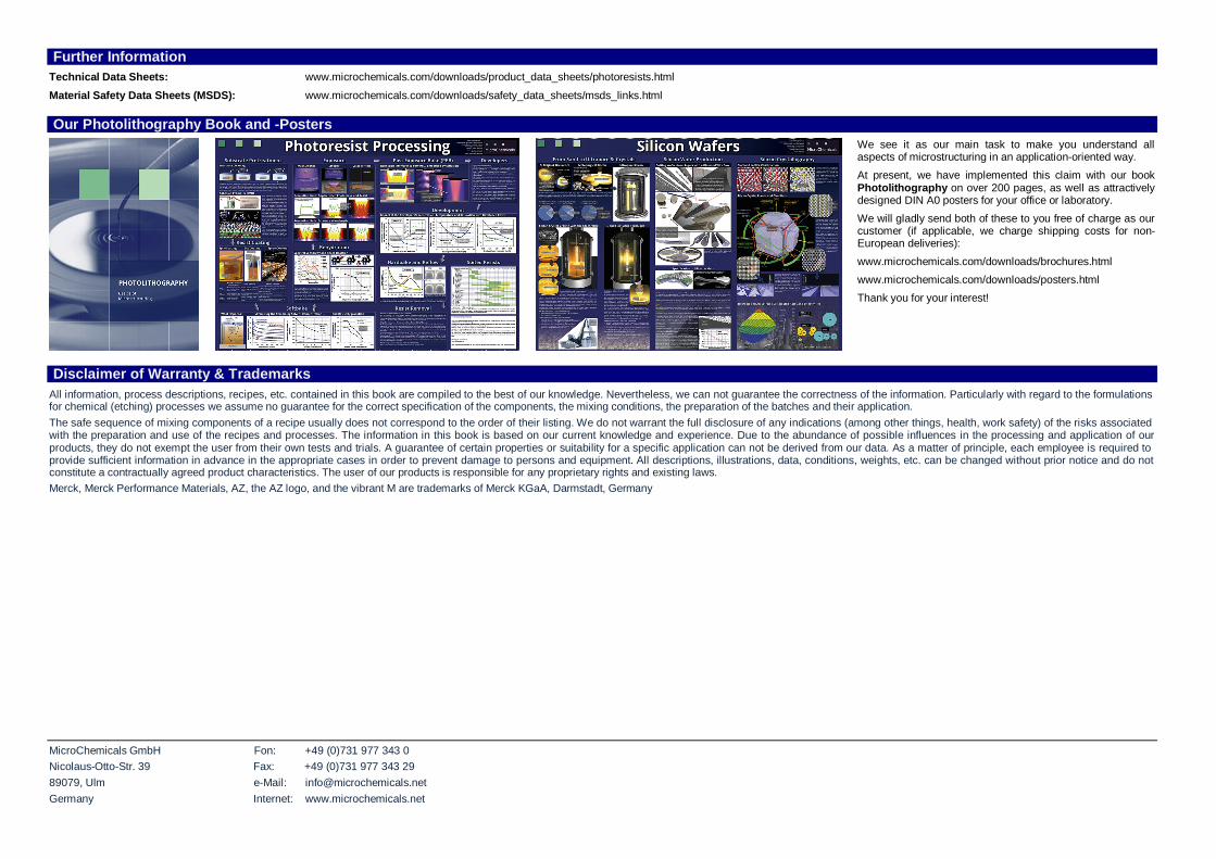
Further Information Technical Data Sheets: www.microchemicals.com/downloads/product_data_sheets/photoresists.html Material Safety Data Sheets (MSDS): www.microchemicals.com/downloads/safety_data_sheets/msds_links.html
Our Photolithography Book and -Posters
We see it as our main task to make you understand all aspects of microstructuring in an application-oriented way. At present, we have implemented this claim with our book Photolithography on over 200 pages, as well as attractively designed DIN A0 posters for your office or laboratory. We will gladly send both of these to you free of charge as our customer (if applicable, we charge shipping costs for non-European deliveries): www.microchemicals.com/downloads/brochures.html www.microchemicals.com/downloads/posters.html Thank you for your interest!
Disclaimer of Warranty & Trademarks All information, process descriptions, recipes, etc. contained in this book are compiled to the best of our knowledge. Nevertheless, we can not guarantee the correctness of the information. Particularly with regard to the formulations for chemical (etching) processes we assume no guarantee for the correct specification of the components, the mixing conditions, the preparation of the batches and their application. The safe sequence of mixing components of a recipe usually does not correspond to the order of their listing. We do not warrant the full disclosure of any indications (among other things, health, work safety) of the risks associated with the preparation and use of the recipes and processes. The information in this book is based on our current knowledge and experience. Due to the abundance of possible influences in the processing and application of our products, they do not exempt the user from their own tests and trials. A guarantee of certain properties or suitability for a specific application can not be derived from our data. As a matter of principle, each employee is required to provide sufficient information in advance in the appropriate cases in order to prevent damage to persons and equipment. All descriptions, illustrations, data, conditions, weights, etc. can be changed without prior notice and do not constitute a contractually agreed product characteristics. The user of our products is responsible for any proprietary rights and existing laws. Merck, Merck Performance Materials, AZ, the AZ logo, and the vibrant M are trademarks of Merck KGaA, Darmstadt, Germany MicroChemicals GmbH Fon: +49 (0)731 977 343 0 Nicolaus-Otto-Str. 39 Fax: +49 (0)731 977 343 29 89079, Ulm e-Mail: [email protected] Germany Internet: www.microchemicals.net