Quantum phase dynamics in an LC shunted Josephson junction · parallel to a Josephson junction...
6
Quantum phase dynamics in an LC shunted Josephson junction Ch. Kaiser, 1,a) T. Bauch, 2 F. Lombardi, 2 and M. Siegel 1 1 Institut fu ¨ r Mikro- und Nanoelektronische Systeme, Karlsruher Institut fu ¨ r Technologie (KIT), Hertzstrabe 16, D-76187 Karlsruhe, Germany 2 Department of Microtechnology and Nanoscience, Chalmers University of Technology, SE-412 96, Go ¨teborg, Sweden (Received 27 October 2010; accepted 9 March 2011; published online 12 May 2011) We have studied both theoretically and experimentally how an LC series circuit connected in parallel to a Josephson junction influences the Josephson dynamics. The presence of the shell circuit introduces two energy scales, which in specific cases, can strongly differ from the plasma frequency of the isolated junction. Josephson junctions were manufactured using the Nb/Al-AlO x /Nb fabrication technology with various on-chip LC shunt circuits. Spectroscopic measurements in the quantum limit show excellent agreement with theory taking into account the shunt inductance and capacitance in the resistively and capacitively shunted junction model. The results clearly show that the dynamics of the system are two-dimensional, resulting in two resonant modes of the system. These findings have important implications for the design and operation of Josephson junction based quantum bits. V C 2011 American Institute of Physics. [doi:10.1063/1.3581139] I. INTRODUCTION Josephson junctions (JJs) are considered to be the main building blocks for a variety of exciting applications, ranging from classical electronics 1 to quantum computing. 2 The phase dynamics of JJs have been well understood for low critical temperature superconductors (LTS). Here, the dy- namics of the system both in the classical and quantum limit are very well reproduced by the resistively and capacitively shunted junction (RCSJ) model 3,4 [see Fig. 1(a)]. However, in some cases this simple model cannot be directly applied to JJs made from high critical temperature superconductors (HTS). The dynamics of HTS JJs are by far more compli- cated. The elaborate phenomenology is based upon intrinsic properties, such as the unconventional d-wave order parame- ter and anisotropic charge transport. 5 Recent measurements performed on a YBa 2 Cu 3 O 7x JJ fabricated using a bi-epitaxial technique on a (110) SrTiO 3 sub- strate have shown that the classic and quantum dynamics of the phase difference across the JJ cannot be described by the conventional RCSJ model. Instead, an extended RCSJ model, including the effect of the stray capacitance and the stray in- ductance, has to be employed [see Figs. 2(a) and 2(b)]. 6,7 Moreover, in LTS quantum circuits large shunt capaci- tors and/or large inductors are intentionally used to influence the properties of the quantum circuit, e.g., large shunting capacitors are used to reduce the plasma frequency of phase qubits 8 or readout superconducting quantum interference devices (SQUIDS). 9 Other designs use an inductor and a ca- pacitor as an isolation network to protect the qubit from its low impedance environment, causing dissipation. 10,11 Our goal is a detailed study of those types of LC shunted junctions which are often found in real experiments. In this case, the dynamics of the junction are modified by the pres- ence of the shell circuit and new effects have to be taken into account. In particular, two energy scales are introduced, which in specific cases, can strongly differ from the plasma frequency of the isolated junction. 7 This has important impli- cations for the quantum mechanical behavior of the system as a whole. In this article, we systematically study the influence of an L S C S shell circuit on the dynamics of a Josephson junc- tion in the quantum limit. We fabricated Nb/Al-AlO x /Nb Josephson junctions shunted by various on-chip inductances, L S , and on-chip capacitances, C S . The high yield of the Nb/ Al-AlO x /Nb technology allows for the fabrication of circuits with extremely well defined junction parameters (critical current density and junction capacitance) as well as electro- magnetic environment parameters, L S and C S , which at the moment is not possible with state of the art HTS JJ fabrica- tion techniques. The article is organized as follows. In Sect. II, we discuss the phase dynamics of a bare Josephson junction according to the RCSJ model. Thereafter, the effect of a shunting LC cir- cuit on the phase dynamics of the whole system is described. Section III contains information about the fabrication of LC shunted Josephson junctions using Nb/Al-AlO x /Nb technol- ogy. The dc electrical properties of the bare Josephson junc- tion and the high frequency characterization of the bare LC resonator are presented in Secs. III A and III B, respectively. The spectroscopic measurements of an LC shunted Joseph- son junction are summarized in Sec. IV, followed by the con- clusions in Sec. V. II. DYNAMICS OF AN LC SHUNTED JOSEPHSON JUNCTION: EXTENDED RCSJ MODEL In this paragraph, we will first review aspects of the phase dynamics in a standard JJ, which can be described a) Author to whom correspondence should be addressed. Electronic mail: [email protected]. 0021-8979/2011/109(9)/093915/6/$30.00 V C 2011 American Institute of Physics 109, 093915-1 JOURNAL OF APPLIED PHYSICS 109, 093915 (2011)
Transcript of Quantum phase dynamics in an LC shunted Josephson junction · parallel to a Josephson junction...

Quantum phase dynamics in an LC shunted Josephson junction
Ch. Kaiser,1,a) T. Bauch,2 F. Lombardi,2 and M. Siegel11Institut fur Mikro- und Nanoelektronische Systeme, Karlsruher Institut fur Technologie (KIT),Hertzstrabe 16, D-76187 Karlsruhe, Germany2Department of Microtechnology and Nanoscience, Chalmers University of Technology,SE-412 96, Goteborg, Sweden
(Received 27 October 2010; accepted 9 March 2011; published online 12 May 2011)
We have studied both theoretically and experimentally how an LC series circuit connected in
parallel to a Josephson junction influences the Josephson dynamics. The presence of the shell
circuit introduces two energy scales, which in specific cases, can strongly differ from the plasma
frequency of the isolated junction. Josephson junctions were manufactured using the Nb/Al-AlOx/Nb
fabrication technology with various on-chip LC shunt circuits. Spectroscopic measurements in the
quantum limit show excellent agreement with theory taking into account the shunt inductance and
capacitance in the resistively and capacitively shunted junction model. The results clearly show
that the dynamics of the system are two-dimensional, resulting in two resonant modes of the
system. These findings have important implications for the design and operation of Josephson
junction based quantum bits. VC 2011 American Institute of Physics. [doi:10.1063/1.3581139]
I. INTRODUCTION
Josephson junctions (JJs) are considered to be the main
building blocks for a variety of exciting applications, ranging
from classical electronics1 to quantum computing.2 The
phase dynamics of JJs have been well understood for low
critical temperature superconductors (LTS). Here, the dy-
namics of the system both in the classical and quantum limit
are very well reproduced by the resistively and capacitively
shunted junction (RCSJ) model3,4 [see Fig. 1(a)]. However,
in some cases this simple model cannot be directly applied
to JJs made from high critical temperature superconductors
(HTS). The dynamics of HTS JJs are by far more compli-
cated. The elaborate phenomenology is based upon intrinsic
properties, such as the unconventional d-wave order parame-
ter and anisotropic charge transport.5
Recent measurements performed on a YBa2Cu3O7�x JJ
fabricated using a bi-epitaxial technique on a (110) SrTiO3 sub-
strate have shown that the classic and quantum dynamics of
the phase difference across the JJ cannot be described by the
conventional RCSJ model. Instead, an extended RCSJ model,
including the effect of the stray capacitance and the stray in-
ductance, has to be employed [see Figs. 2(a) and 2(b)].6,7
Moreover, in LTS quantum circuits large shunt capaci-
tors and/or large inductors are intentionally used to influence
the properties of the quantum circuit, e.g., large shunting
capacitors are used to reduce the plasma frequency of phase
qubits8 or readout superconducting quantum interference
devices (SQUIDS).9 Other designs use an inductor and a ca-
pacitor as an isolation network to protect the qubit from its
low impedance environment, causing dissipation.10,11
Our goal is a detailed study of those types of LC shunted
junctions which are often found in real experiments. In this
case, the dynamics of the junction are modified by the pres-
ence of the shell circuit and new effects have to be taken into
account. In particular, two energy scales are introduced,
which in specific cases, can strongly differ from the plasma
frequency of the isolated junction.7 This has important impli-
cations for the quantum mechanical behavior of the system
as a whole.
In this article, we systematically study the influence of
an LSCS shell circuit on the dynamics of a Josephson junc-
tion in the quantum limit. We fabricated Nb/Al-AlOx/Nb
Josephson junctions shunted by various on-chip inductances,
LS, and on-chip capacitances, CS. The high yield of the Nb/
Al-AlOx/Nb technology allows for the fabrication of circuits
with extremely well defined junction parameters (critical
current density and junction capacitance) as well as electro-
magnetic environment parameters, LS and CS, which at the
moment is not possible with state of the art HTS JJ fabrica-
tion techniques.
The article is organized as follows. In Sect. II, we discuss
the phase dynamics of a bare Josephson junction according to
the RCSJ model. Thereafter, the effect of a shunting LC cir-
cuit on the phase dynamics of the whole system is described.
Section III contains information about the fabrication of LCshunted Josephson junctions using Nb/Al-AlOx/Nb technol-
ogy. The dc electrical properties of the bare Josephson junc-
tion and the high frequency characterization of the bare LCresonator are presented in Secs. III A and III B, respectively.
The spectroscopic measurements of an LC shunted Joseph-
son junction are summarized in Sec. IV, followed by the con-
clusions in Sec. V.
II. DYNAMICS OF AN LC SHUNTED JOSEPHSONJUNCTION: EXTENDED RCSJ MODEL
In this paragraph, we will first review aspects of the
phase dynamics in a standard JJ, which can be described
a)Author to whom correspondence should be addressed. Electronic mail:
0021-8979/2011/109(9)/093915/6/$30.00 VC 2011 American Institute of Physics109, 093915-1
JOURNAL OF APPLIED PHYSICS 109, 093915 (2011)

within the framework of the RCSJ model12 [Fig. 1(a)].
Here, the junction inductance, LJ , and capacitance, CJ , act
as an anharmonic LC resonator (at zero voltage) with reso-
nance frequency xP ¼ LJCJð Þ�1=2. Assuming a sinusoidal
current phase relation, the Josephson inductance is given by
LJ ¼ /0= 2p IC cos / ¼ LJ0=cos /, where IC is the critical
current, / is the gauge-invariant phase difference across the
junction and /0 ¼ h=2e is the superconducting flux quan-
tum, with e being the elementary charge and h being
Planck’s constant. For a finite bias current, the fictitious
phase particle with mass m ¼ /0=2pð Þ2CJ may escape from
a metastable well in the junction potential either by thermal
activation or by tunneling through the potential barrier [see
Fig. 1(b)]. This corresponds to the junction switching from
the zero voltage state to a finite voltage state. At low tem-
perature, the escape is dominated by tunneling.13 For tem-
peratures smaller than the energy level separation of the
quasibound states in the well, only the ground state is popu-
lated. The quantum states can be spectroscopically
observed by inducing a resonant transition between the
ground state and the excited states by applying microwaves
having frequencies f0n ¼ En � E0ð Þ=h.14 The bias current
dependence of the transition frequency between the ground
state and the first excited state can be approximated by the
plasma frequency of small oscillations at the bottom of the
well
2pf01 � xP ¼ffiffiffiffiffiffiffiffiffiffiffi2pIC
/0CJ
s1� I
IC
� �2" #1=4
¼ xP0 1� c2� �1=4
:
(1)In the following, we will show how an LSCS shell circuit
connected to a JJ [see Fig. 2(a)] affects the phase dynamics
of the system as a whole.
In Fig. 2(a), the phase difference across the Josephson
junction is given by /J . We can define /S ¼ 2p=ð/0Þ=ISLS þ /J , where IS is the current through the inductor.
Neglecting dissipative elements in the circuit, we can write
the normalized equation of motion as7
€/J þ sin /J þ/J � /S
b¼ 0; (2)
v�1 €/S þ/S � /J
b¼ c : (3)
Here, time is normalized to the zero-bias plasma fre-
quency of the Josephson junction xP0 ¼ffiffiffiffiffiffiffiffiffiffiffiffiffiffiffiffiffiffiffiffiffiffi2pIC=/0CJ
p,
c ¼ I=IC is the normalized bias current, b ¼ LS=LJ0
denotes the ratio between the shell inductance and the
zero-bias Josephson inductance LJ0 ¼ /0=2p IC, and
v ¼ CJ=CS is the ratio between the junction capacitance
and the shell capacitance.
As can be seen from Eqs. (2) and (3), the dynamics are
described by two variables, /J and /S. Consequently, the
simple picture of a fictitious phase particle moving in a one-
dimensional potential, as shown in Fig. 1(a), is in general, no
longer valid. Instead, the dynamics have to be described by a
particle moving in a two-dimensional potential [see Fig.
2(b)],7 which results in two normal modes (or resonance fre-
quencies) of the system. From Eqs. (2) and (3), the resonance
frequencies of the two normal modes of the LC shunted JJ
(LCJJ) can be derived.
Here, we will only consider the limiting case, v� 1,
where the shell capacitance is much larger than the junction
capacitance. This limiting case is common to many quantum
devices containing Josephson junctions such as phase qubits8
or readout SQUIDs of flux qubits,9 along with HTS Joseph-
son junctions.6
The general expression for the upper and the lower reso-
nant mode is given by6
FIG. 1. (a) Circuit diagram of a current biased JJ in the RCSJ model. Damp-
ing of the JJ due to the environment and due to intrinsic effects is described
by an admittance, Y. (b) Energy levels in the potential of the current biased
JJ. Microwave radiation induces a transition from the ground state to the first
excited state having a larger escape rate than the ground state.
FIG. 2. (Color online) (a) Circuit diagram of an LC shunted JJ. (b) Two-
dimensional potential, U (for details, see Ref. 7), of an LC shunted JJ for a
bias current of I ¼ 0:5IC, CS ¼ 10CJ , and LS ¼ 10LJ0. Here, EJ ¼ U0IC=2pdenotes the Josephson coupling energy.
093915-2 Kaiser et al. J. Appl. Phys. 109, 093915 (2011)

x6 ¼ xP0
ffiffiffiffiffiffiffiffiffiffiffiffiffiffiffiffiffiffiffiffiffiffiffiffiffiffiffiffiffiffiffiffiffiffiffiffiffiffiffiffiffiffiffiffiffiffiffiffiffiffiffiffiffiffiffiffiffiffiffiffiffiffiffiffiffiffiffiffiffiffiffiffiffiffiffiffiffiffiffiffiffiffiffiffiffiffiffiffiffiffiffiffiffiffiffiffiffiffiffiffiffiffiffiffiffiffiffiffiffiffiffiffiffiffiffiffiffi1þ b
ffiffiffiffiffiffiffiffiffiffiffiffiffi1� c2
pþ v6
ffiffiffiffiffiffiffiffiffiffiffiffiffiffiffiffiffiffiffiffiffiffiffiffiffiffiffiffiffiffiffiffiffiffiffiffiffiffiffiffiffiffiffiffiffiffiffiffiffiffiffiffiffiffiffiffiffiffiffiffiffiffiffiffiffiffiffiffiffiffiffiffi1þ b
ffiffiffiffiffiffiffiffiffiffiffiffiffi1� c2
pþ v
� �2
�4bvffiffiffiffiffiffiffiffiffiffiffiffiffi1� c2
pr2b
vuuut:
For v� 1, the lower resonance mode can be approximated
by
x� ¼1ffiffiffiffiffiffiffiffiffiffiffiffiffiffiffiffiffiffiffiffiffiffiffiffi
LS þ LJð ÞCS
p ; (4)
while the approximation for the upper resonance mode yields
xþ ¼
ffiffiffiffiffiffiffiffiffiffiffiffiffiffiffiffiffiffiffiffiffiffiffiffiffiffiffiffiffi1
LJþ 1
LS
� �1
CJ
s: (5)
It follows directly that for b� 1, the upper resonant mode,
xþ, can be well approximated by the eigenfrequency of the
Josephson junction, LJCJð Þ�1=2, whereas the lower resonance
mode, x�, is given by the resonance frequency of the shell
circuit, LSCSð Þ�1=2. This reflects the fact that for b� 1, the
bare junction mode and the LC mode are decoupled. From
the point of view of novel phase dynamics and effects, the
most interesting case is the one for v� 1 and not too large
values of b. For b ¼ 1 and b ¼ 10, the theoretically expected
eigenfrequencies, x� and xþ, are shown in Fig. 3 and com-
pared to the pure Josephson plasma frequency xP. The nonli-
nearity (nonvanishing bias current dependence) of both the
upper and lower resonant modes clearly indicate that for
b � 10, the bare junction mode and the LSCS mode are
strongly coupled.
It is worth pointing out that the lower resonant mode,
x�, might be used for a phase qubit with improved dephas-
ing times compared to a bare Josephson junction. This can
be directly seen from the insets in Figs. 3(a) and 3(b).
Dephasing is mainly caused by low frequency fluctuations
in the biasing parameter, which in our case is the bias cur-
rent. The dephasing rate is given by, C/ � DIn @x=@Ið Þ,where DIn is the amplitude of the low frequency current
noise. We see that a system having a flatter bias current de-
pendence of the resonant mode will be less sensitive to bias
current fluctuations. Therefore, a large value of b is desira-
ble. However, this value should not be too large, since for
increasing b, the anharmonicity of the system is reduced,
which makes a two-level approximation of the quantum
system cumbersome.
III. SAMPLE FABRICATION
The samples were fabricated using a combined photoli-
thography/electron-beam lithography process. First, the Nb/
Al-AlOx/Nb trilayer was DC magnetron sputtered in situwith layer thicknesses of 100 nm/7 nm/100 nm. In order to
obtain a critical current density of �80 A/cm2, the Al oxida-
tion parameters were chosen accordingly. After that, the
form of the bottom junction electrodes (including one half of
the inductor and the bottom capacitor plate) were patterned
by photolithography and reactive-ion-etching (RIE) as well
as ion-beam etching. Then the JJs were defined by a negative
e-beam lithography process and subsequently etched by RIE.
Using the same resist mask, the following anodic oxidation
with a voltage of 20 V created an Nb2O5 layer of about 50
nm in thickness for the first insulation layer of both the
FIG. 3. (Color online) Plasma frequency, xP, for a single junction, upper
normal mode, xþ, of the LCJJ system, and lower normal mode, x�, of the
LCJJ system. The insets show a magnification of the lower mode close to
c ¼ 1. (a) For v ¼ 0:1 and b ¼ 1. (b) For v ¼ 0:1 and b ¼ 10.
FIG. 4. (Color online) (a) Photo of an LCJJ8-type sample. The capacitor is
situated on the left while the JJ can be found on the right. The two meander
lines connecting these elements act as inductors. The bottom electrode is
shown on the upper part of the picture and has changed color due to the an-
odic oxidation. (b) SEM image of the Josephson junction. The SiO insula-
tion layer can be seen as the dark circle.
093915-3 Kaiser et al. J. Appl. Phys. 109, 093915 (2011)
junction and the capacitor. The second insulating layer of
SiO was patterned by a positive e-beam lithography process,
thermal evaporation of the SiO onto the cooled samples, and
a subsequent lift-off process. Finally, the wiring layer (acting
as the top electrode of the capacitor and the second part of
the inductor) was deposited by DC magnetron sputtering and
patterned by photolithography. A photo of a typical sample
can be seen in Fig. 4(a), while an SEM image of the JJ itself
is shown in Fig. 4(b). All junctions used within this work
were round in shape and had a diameter of �3 lm, indicating
that they had a capacitance of CJ �0.4 pF and a Josephson
inductance of LJ0�0.06 nH.
A. Characterization of a single Nb/Al-AlOx/NbJosephson junction
As a first step, single Nb/Al-AlOx/Nb JJs with parame-
ters identical to the ones used for the final spectroscopic
measurements on LC shunted JJs were fabricated and charac-
terized in order to see if a sufficient quality and reproducibil-
ity could be reached. As expected, the use of electron-beam
lithography led to no significant spread in JJ sizes and critical
currents, Ic. The junctions were characterized at 4.2 K and
the commonly used quality factor, Rsg/RN, was evaluated (RN
being the junction’s normal resistance and Rsg its subgap re-
sistance evaluated at a voltage of 2 mV). For all junctions,
we found Rsg/RN> 35, which indicates a very high quality.
For further characterization at the temperature of the final
quantum experiment, the junctions were cooled down to 18
mK. A typical current-voltage characteristic at this tempera-
ture is shown in Fig. 5. We found no excess currents and a
high IcRN product of 1.73 mV, meaning that we observed
clear and clean Cooper pair tunneling.15 Furthermore, meas-
urements with a voltage bias setup also showed very low
leakage currents at 18 mK, as can be seen in the inset of Fig.
5. The high gap voltage of Vgap¼ 2.93 mV indicates that the
Nb electrodes are of high quality. Furthermore, the modula-
tion of the critical current with an external magnetic field
(not shown) showed an Airy-like pattern, as expected for a
circular JJ. This indicates that the bias current is homogene-
ously distributed inside the junction.
B. Characterization of the LSCS shell circuit
In the following, the design, simulation, and characteri-
zation of the external shell circuits will be described. For the
calculation of the shell capacitance values, the simple plate
capacitor formula was used. As we aimed for a ratio of Cs/
CJ¼ 10, an overlay area of 0.02 mm2 was chosen, so that
Cs¼ 3.7 pF. The calculation of the inductance values, how-
ever, is more subtle. First, the kinetic inductance of the
superconducting Nb lines has to be taken into account. Sec-
ond, we found the inductance values to be frequency depend-
ent for some of our desired shell circuits. We designed and
simulated our structures with SONNET16 for a wide frequency
range, taking Nb material parameters into account. The in-
ductance value was taken at the point where the simulation
frequency and the expected lower resonant mode frequency
of the final LCJJ circuit matched. Here, we chose the lower
resonant mode since it has a stronger deviation from the bare
RCSJ plasma frequency for b� 1 [see Fig. 3(b)]. Eight dif-
ferent inductance geometries were designed, ranging from
short straight lines to relatively narrow meanders [see Fig.
4(a)], leading to Ls values from 0.17 to 16 nH. This means
that we could cover a wide range of LS/LJ ratios, systemati-
cally increasing from b�3 for sample LCJJ1 to b�270 for
sample LCJJ8.
In order to see whether the simulation values were reli-
able, we fabricated LC shell circuits having the same design
as the final samples, but replaced the Josephson junctions
with a superconducting shortcut. Furthermore, a small gap
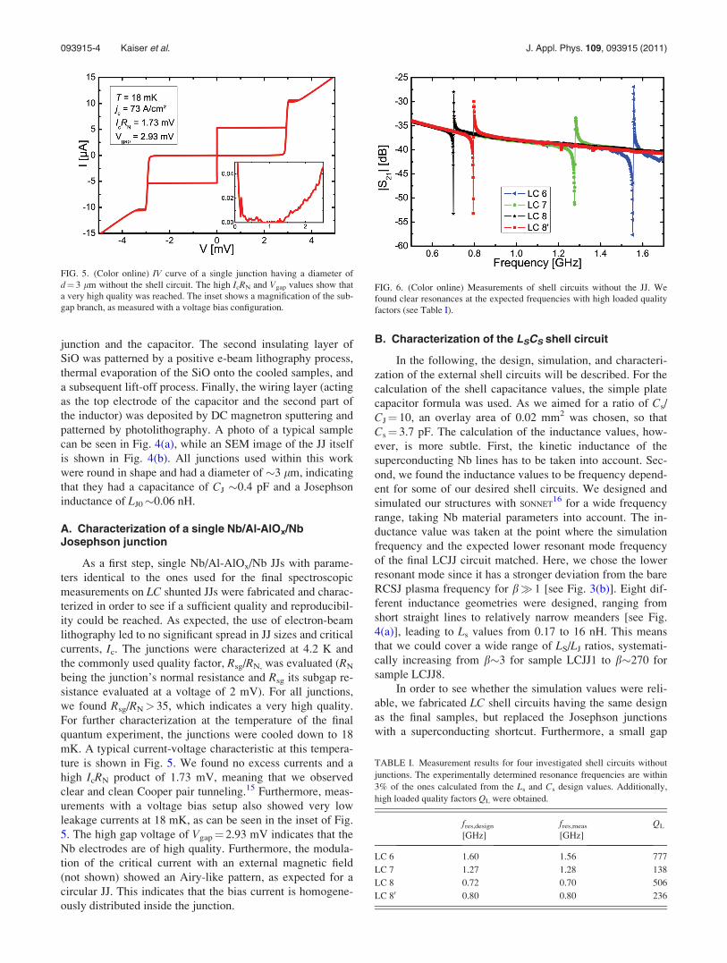
FIG. 5. (Color online) IV curve of a single junction having a diameter of
d¼ 3 lm without the shell circuit. The high IcRN and Vgap values show that
a very high quality was reached. The inset shows a magnification of the sub-
gap branch, as measured with a voltage bias configuration.
FIG. 6. (Color online) Measurements of shell circuits without the JJ. We
found clear resonances at the expected frequencies with high loaded quality
factors (see Table I).
TABLE I. Measurement results for four investigated shell circuits without
junctions. The experimentally determined resonance frequencies are within
3% of the ones calculated from the Ls and Cs design values. Additionally,
high loaded quality factors QL were obtained.
fres,design fres,meas QL
[GHz] [GHz]
LC 6 1.60 1.56 777
LC 7 1.27 1.28 138
LC 8 0.72 0.70 506
LC 80 0.80 0.80 236
093915-4 Kaiser et al. J. Appl. Phys. 109, 093915 (2011)

was etched into one of the bias lines leading to the LC cir-
cuit, so that a coupling capacitor, Cc, was formed, which
would sufficiently decouple the LC circuit from the low-im-
pedance environment. The experimental test of our designs
was especially important for the structures with narrow me-
ander lines, in order to exclude the possibility that a spurious
capacitive coupling between the lines would shift the reso-
nance or degrade its quality factor. For this purpose, we
designed and fabricated a printed circuit board that allowed
measurements up to about 2 GHz, which was enough to test
the three smallest resonance frequencies and hence, the three
largest inductors. For one design, the resonance frequency
was slightly varied by adjusting the SiO thickness, so that
two samples, LC8 and LC80, were obtained. These prelimi-
nary measurements were carried out in liquid helium at
4.2 K. The chips were glued onto the printed circuit board
and contacted by Al bonding wires. The PC board was con-
tacted via mini-SMP connectors and 50 X cables to an Agi-
lent Network Analyzer, which was used to measure the
transmission S-parameter, |S21|. The results of the measure-
ment are shown in Fig. 6 and Table I. It can be seen that we
obtained excellent agreement between expected and experi-
mentally determined resonance frequencies. This confirms
the precision of our simulation method and excludes capaci-
tive parasitics of any kind. We can conclude that if we have
such excellent agreement even for the complex high-induct-
ance structures (i.e., samples LC6–LC8), the parameters of
the low-impedance structures containing simple straight lines
as inductors (i.e., samples LC1–LC5), should also be well-
defined. Furthermore, we obtained high loaded quality fac-
tors, QL, which were probably only limited by the Cc values,
which were not well-defined. This means that the shell cir-
cuits exhibit low damping, which is crucial for the observa-
tion of the under-damped dynamics of the LCJJ systems.
IV. MEASUREMENT OF AN LC SHUNTED NB/AL-ALOX/NB JOSEPHSON JUNCTION
The measurements of an LCJJ were performed in a
dilution refrigerator with a base temperature of 15 mK. The
dc-lines connecting the sample to the room temperature
electronics were filtered with passive RCL filters at the 1 K
stage and with copper powder filters at the mixing chamber
stage.17
The design parameters of the investigated LCJJ system
are given in Table II.
At T � 20mK, which is clearly below the crossover
temperature from the thermal to the quantum regime, micro-
waves were applied to the LCJJ in order to observe resonant
activation of the phase dynamics.14 These measurements
allow us to analyze the bias current dependence of the
energy level separation.
For such spectroscopy experiments, it is likely that proc-
esses of higher order will also be observed. These can be
multiphoton and/or multilevel processes.18 This leads to
transitions at microwave frequencies, 2pfmw � p=qð Þx6.
Other processes of higher order are mixed transitions such
as, 2pfmw � p=qð Þxþ6 m=nð Þx� (p; q;m and n are integers).
The equality is only true for p¼ 1 and m¼ 1 as the anharmo-
nicity of the potential causes the level spacing to shrink for
increasing excitation levels p and m.
Spectroscopy measurements were carried out on sample
LCJJ2 to reveal whether the two orthogonal resonant modes
x� and xþ would be observed instead of the plasma fre-
quency of the single junction. The measurement results are
shown in Fig. 7. Here, we can clearly identify the contribu-
tions of the two resonance modes. In the same graph, theoret-
ically calculated curves according to Eqs. (4) and (5) are
shown. It can be seen that the measurement data are in excel-
lent agreement with the theoretical curves. Furthermore, no
data points corresponding to the single junction were found,
except where modes of the single junction and modes of the
FIG. 7. (Color online) Spectroscopy data (gray points) of sample LCJJ2
without an applied magnetic field. An excellent agreement between the
experiment on one side and design values and theory on the other side is
observed.
TABLE II. Design parameters of an LC shunted Josephson junction.
Sample
jC IC d CJ CS v LJ0 LS b[A/cm2] [lA] [lm] [pF] [pF] [] [pH] [nH] []
LCJJ2 77 5.48 3.01 0.38 3.7 0.10 60 0.48 8.0
FIG. 8. (Color online) Spectroscopy data (gray points) of sample LCJJ2
with an applied magnetic field, suppressing the critical current to Ic¼ 3.82
lA. The agreement between theory and experiment is excellent.
093915-5 Kaiser et al. J. Appl. Phys. 109, 093915 (2011)

LCJJ system cross, which is visible, in particular, at half the
plasma frequency, fp/2. Since no data points were found in
regions of the spectrum where only single junction modes
would be expected, we attribute the points at the crossings to
the corresponding LCJJ modes. Altogether, our measure-
ments provide strong evidence that the LCJJ system is very
well described by theory and acts indeed as one single quan-
tum system. This is remarkable since the circuit has a size of
200 � 650 lm2.
All theoretical curves in Fig. 7 were calculated using one
fixed set of parameters. For the junction these were a critical
current of IC¼ 6.53 lA, and a Josephson capacitance of
CJ¼ 0.38 pF. For the shell circuit, the parameters accounted
for LS¼ 0.43 nH and CS¼ 3.7 pF. This means that, effec-
tively, v¼ 0.10 and b¼ 8.5. The values used to fit the experi-
mental spectroscopic data and the design values given in
Table II are in excellent agreement. Only the critical current
was slightly higher and the shell inductor slightly lower than
planned. This shows that the parameters of our Josephson
junction circuits are completely under control and the quan-
tum properties of the circuits can be designed at will.
On the same LCJJ, the critical current was suppressed to
Ic¼ 3.82 lA by applying a magnetic field and the same spec-
troscopy measurements were repeated. The measurement
results are shown in Fig. 8. All theoretical curves in this
graph were calculated with the same parameters as in the ab-
sence of the magnetic field. Again, we have excellent agree-
ment between the measurement data and theoretical
expectation. This further confirms our conclusion that the LCcircuit strongly affects the phase dynamics of a Josephson
junction.
V. CONCLUSIONS
We have shown that a Josephson junction shunted by an
inductance and a capacitance indeed acts as one single quan-
tum system. This is remarkable since the circuit has a size of
200�650 lm2, which is larger than most superconducting
qubits. Furthermore, we found excellent agreement between
the measurement data and the theoretically expected behavior
calculated by using the design parameters. The findings show
that such an LCJJ system has indeed two new energy scales
instead of the energy scale of a single Josephson junction. Our
results are important for understanding the dynamics in high-
temperature Josephson junctions, where such shunting ele-
ments cannot be avoided when substrates with high dielectric
constants are involved. Furthermore, the findings are impor-
tant for superconducting quantum circuits such as quantum
bits. When such systems are capacitively shunted by Cs, it is
mostly assumed that Ls¼ 0 (which is definitiely not the case
since all electrical connections exhibit an inductance) and
xP ¼ x� ¼ LJCSð Þ�1=2. We have shown that Ls needs to be
considered, resulting in x� ¼ LJ þ LS½ CSð Þ�1=2and that
there is a second energy scale in the system, namely,
xþ ¼ 1=LJ þ 1=LS½ =CJð Þ1=2. This is an important result for
quantum device design and operation.
ACKNOWLEDGMENTS
This work was partly supported by the Deutsche For-
schungsgemeinschaft Center for Functional Nanostructures
(Project No. B3.4), the Swedish Research Council (VR),
EU STREP project MIDAS, and the Knut and Alice Wal-
lenberg Foundation. F.L. was supported by a grant from the
Knut and Alice Wallenberg Foundation. Furthermore, we
would like to thank M. Birk for help with inductor simula-
tion, D. Bruch for the design of the printed circuit board,
and J. Czolk and T. Wienhold for help with LC circuit
characterization.
1T. van Duzer, Principles of Superconductive Devices and Circuits, 2nd ed.
(Prentice Hall, Upper Saddle River, NJ, 1999).2Y. Makhlin, G. Schon, and A. Shnirman, Rev. Mod. Phys. 73, 357 (2001).3W. C. Stewart, Appl. Phys. Lett. 12, 277 (1968).4D. E. McCumber, J. Appl. Phys. 39, 3113 (1968).5C. C. Tsuei and J. R. Kirtley, Rev. Mod. Phys. 72, 969 (2000).6T. Bauch, T. Lindstrom, F. Tafuri, G. Rotoli, P. Delsing, T. Claeson and
F. Lombardi, Science 311, 57 (2006).7G. Rotoli, T. Bauch, T. Lindstrom, D. Stornaiuolo, F. Tafuri, and F. Lom-
bardi, Phys. Rev. B 75, 144501 (2007).8M. Steffen, M. Ansmann, R. McDermott, N. Katz, R. C. Bialczak,
E. Lucero, M. Neeley, E. M. Weig, A. N. Cleland, and J. M. Martinis,
Phys. Rev. Lett. 97, 050502 (2006).9A. Lupascu, C. J. M. Verwijs, R. N. Schouten, C. J. P. M. Harmans, and J.
E. Mooij, Phys. Rev. Lett. 93, 177006 (2004).10A. J. Berkley, H. Xu, M. A. Gubrud, R. C. Ramos, J. R. Anderson, C. J.
Lobb, and F. C. Wellstood, Phys. Rev. B 68, 060502 (2003).11J. Claudon, F. Balestro, F. K. J. Hekking, and O. Buisson, Phys. Rev. Lett.
93, 187003 (2004).12M. Tinkham, Introduction to Superconductivity, 2nd ed. (McGraw-Hill,
New York, 2004).13A. O. Caldeira and A. J. Leggett, Phys. Rev. Lett. 46, 211 (1981).14M. H. Devoret, D. Esteve, C. Urbina, J. Martinis, A. Creland, and J. Clarke,
in Quantum Tunneling in Condensed Media, edited by Y. Kagan and A. J.
Leggett (North-Holland, Amsterdam, 1992).15V. Ambegaokar and A. Baratoff, Phys. Rev. Lett. 10, 486 (1963).16Sonnet Software Inc., 1020 Seventh North Street, Suite 210, Liverpool,
NY 13088, USA.17T. Bauch, F. Lombardi, F. Tafuri, A. Barone, G. Rotoli, P. Delsing, and T.
Claeson, Phys. Rev. Lett. 94, 087003 (2005).18A. Wallraff, T. Duty, A. Lukashenko, and A. V. Ustinov, Phys. Rev. Lett.
90, 037003 (2003).
093915-6 Kaiser et al. J. Appl. Phys. 109, 093915 (2011)