PV solar energy - from macro to the nano - Materials UK … solar energy SJCI.pdfCdZnS/CdTe device...
28
CSER Solar Photovoltaics Professor Stuart Irvine, Centre for Solar Energy Research (CSER), OpTIC Technium Materials Supply Chains in the UK Power Generation Sector 1 st May 2008
Transcript of PV solar energy - from macro to the nano - Materials UK … solar energy SJCI.pdfCdZnS/CdTe device...

CSER
Solar Photovoltaics
Professor Stuart Irvine, Centre for Solar Energy Research
(CSER), OpTIC
Technium
Materials Supply Chains in the UK Power Generation Sector 1st
May 2008

CSER
Summary of presentation•
The global expansion in PV industry
•
The cost barrier to adoption•
The industry supply scene in PV Solar Energy –
do we have a PV industry in the
UK?•
The PV Supergen
research project and
second generation thin film PV•
Conclusions

CSER
Quote from European PV industry road map
•
Solar cells, the basic elements of photovoltaics (PV), convert light energy directly into electric energy. This one step process is clean and absolutely emission-
free: it is a modular electricity source that can be installed in every power size from microwatt to multi-megawatt scales. Therefore, it is ideally suited for distributed generation of electricity near the user, everywhere around the globe.

CSER
The global expanding PV industry
0
500
1000
1500
2000
2500
3000
3500
MW
2000 2002 2004 2006 2008 2010
YEAR
Installed MWPredicted MW
Over 90% current PV production is crystalline Si, thin film is set to take a larger share
In 2001 46% was on grid domestic. Predicted to become 66% in 2010

CSER
Who is buying PV?
Sales in 2005
Large adopters use favourable feed-in tarriffs

CSER
The energy price profileE
uro/
kWh
From European PV Industry Association Road Map

CSER
How to reduce cost of PV production
0.00
0.50
1.00
1.50
2.00
2.50
1 2 3 4log(capacity in MW)
€/W
totalequipmentmaterialstaff
Cost model of Dieter Bonnet for thin film CdTe
solar modules PV21
Current thin filmCurrent wafer silicon
Very large scale – materials cost
dominate

CSER
Wales as a centre for PV industry•
Sharp (crystalline silicon) in North Wales; www.sharp.co.uk
•
G24i(dye sensitised) in Cardiff-capital of Wales: www.g24i.com
•
Solar Century (PV roof tiles and installation) in south Wales: www.solarcentury.co.uk
•
Dulas (PV systems and installation) in West Wales: www.dulas.org.uk
•
Epod Solar Wales (thin film silicon) South Wales: www.epodsolar.com
•
PV Systems (Installers) South Wales: www.pvsystems.com
•
IQE (III-V epitaxy
for concentrator cells) South Wales: http://www.iqep.com/
•
Dysol (dye sensitised) European Centre in OpTIC
Technium•
Corus Colours (PV coatings on sheet steel)

CSER
Sharp the world’s leading manufacturer
Sharp module factory near Wrexham now manufacturing 220 MW per year for the European market.
Eden Centre, CornwallCIS Tower, Manchester

CSER
Solar Century PV roof tile

CSERExample of thin film PV façade at
OpTIC
Technium, St AsaphThe PV façade at OpTIC
Technium
demonstrates novel thin film CIGS technology
1000 m2
generating up to 85 kWp
of completely clean
energy.Largest of its kind outside US
In the first 12 months of operation a total of 65,000 kWh of clean electricity was generated, saving 28 tonnes of carbon emissions from fossil fuelled power stations

CSER
PV Road map for Wales•
Recognises importance of developing PV industry while increasing PV adoption.
•
The WOF Photovoltaics group believes that a target
of at least 10% of renewable energy generated via PV in Wales by the year 2020 is a realistic expectation.
•
875MW installed capacity is equivalent to around 437,000 houses each with small 2kW rooftop installations

CSER
WERC PV TASK GROUP•
Aims to enable large scale PV adoption through innovative systems level technology, the PV TG membership includes:
•
Sharp•
Wales school of architecture
•
Corus(Tata) steel roofs•
Redrow
-
house builders
•
Dulas
–
PV systems integration•
Optic technium
-
innovation centre
•
University of Wales -
centres of excellence at NEWI, Swansea and Cardiff
•
Welsh Assembly Government
Aim to accelerate innovation through supply chain teaming

CSER
Proposed OpTIC
Technology Park with dedicated Solar Energy Technology Centre

CSER
Challenge for UK research programme on PV materials
•
Find ways of using thinner wafers of crystalline silicon.
•
Pave way for high volume, in-line processing.
•
Improve efficiency of thin film polycrystalline materials.
•
Investigate ultra-thin absorbers.

CSER
EPSRC funded PV Supergen project “PV Materials for the 21st Century” Renewal Project started April 2008
Mission statement: to make a major contribution to
achieving competitive PV solar energy.

CSER
PV PV SupergenSupergen Renewal Renewal ££6.2m over 4 years6.2m over 4 years
STRATEGY
Build on achievements in Phase I
Sharpen focus on thin film PV
Contextualize research within the framework of long term sustainability
Exploit UK strength in nanotechnology for novel PV concepts
EXPECTATIONS
Establish internationally leading position in PV based on sustainable materials
Consolidate world leading position in novel approaches to light management
Transfer IP to industry as technologies move towards maturity
Develop a deeper understanding of the techno-economic context of the research

CSER
PV21 Renewal project team members
•
Ken Durose, Durham•
Stuart Irvine, Bangor
•
Laurie Peter, Bath•
Tom Markvart, SES Southampton
•
Darren Bagnall, ECS Southampton
•
Ian Forbes, Northumbria•
Robert Gross, IC
-new
•
Mark Winskel, Edinburgh -new•
Hari Reehal, Southbank -new David Lane, Cranfield
-new
•
Pilkington -new•
First Solar -new
•
SemiMetrics
-new•
Kurt J Lesker
Company
•
Plasma Quest -new•
SAFC Hitech
•
Millbrook•
CSMA Mats
•
Sharp –new public awareness and engagement

CSER
Integration of Industrial partnersIndustrial Exploitation route
Participating company
Materials Supply Pilkington, SAFC (Epichem)
Materials Characterisation
SemiMetrics, MATS CMS, Millbrook
Processing tools Kurt J Lesker, Plasma Quest
PV Production First Solar, NAREC, (BP Solar, EPOD Solar Wales)

CSER
Stronger links needed to technology exploitation
Low Investment High
Focus on limited range
Research Development Demonstration pilot production
PV21 renewal programme
High uncertainty Low
Large range of experiments
CSER
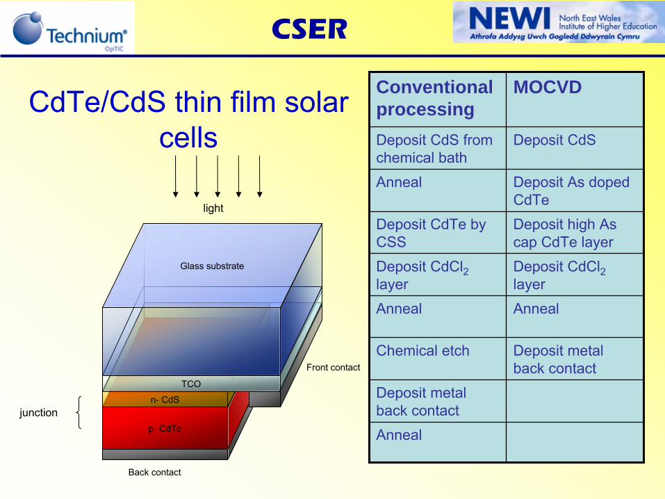
p-
CdTe
n-
CdS
TCO
Glass substrate
Front contact
Back contact
junction
light
Conventional processing
MOCVD
Deposit CdS
from chemical bath
Deposit CdS
Anneal Deposit As doped CdTe
Deposit CdTe
by CSS
Deposit high As cap CdTe
layerDeposit CdCl2
layer
Deposit CdCl2
layer
Anneal Anneal
Chemical etch Deposit metal back contact
Deposit metal back contactAnneal
CdTe/CdS
thin film solar cells

CSER
MOCVD is enabling thinner CdTe
solar cells than those currently in production
SEM of cross section of Sb2 Te3 /CdTe/CdS/TCO/glass solar cell structure.
SEM by Dr Mike Cousins, Durham UniversityMaterial from ANTEC GmbH
SEM of CdTe/CdS/ITO/glass
from MOCVD grown devices
2 µm
10-12% AM1.5

CSER
Potential for increasing the capture of solar radiation in CdTe
solar cells
Spe
ctra
l Irr
adia
nce
/ W
m-2
nm -1
arbi
trar
y in
tens
ity
/ co
unts
A graph of the Standard AM1.5 global irradiance 100mW/cm2
Wavelength (nm)
0.0000E+00
2.0000E-01
4.0000E-01
6.0000E-01
8.0000E-01
1.0000E+00
1.2000E+00
1.4000E+00
1.6000E+00
1.8000E+00
200.0 300.0 400.0 500.0 600.0 700.0 800.0 900.0 1000.0 1100.0 1200.0
AM1.5
Max Jsc =30.8
mA/cm2
Cut off at 500nm due to CdS
band gap
Extend λ

CSER
0
0.0005
0.001
0.0015
0.002
0.0025
0.003
1.50 2.00 2.50 3.00 3.50 4.00
3.55 eV
3.50 eV
3.32 eV2.9 eV2.58 eV
(αE)
2 (m
-2eV
2 )
Energy (eV)
Increasing (x) in Cd(1-x) Z(x) S by increasing DEZn/DMCd
ratio
Replace CdS
layer with CdZnS
to increase band gap
Optical transmission measurements
Eurig Jones et al presented at MC8 conference

CSER
Improved Spectral response of CdZnS/CdTe
PV devices
This shows that the blue-end is heavily absorbed by the CdS, dropping rapidly at 500nm to less than 10% QE.
0
0.2
0.4
0.6
0.8
1
1.2
400 450 500 550 600 650 700 750 800 850 900
QE
Wavelength (nm)
CdZnS/CdTe device CdS/CdTe device
Wavelength (nm)
Blue is not as heavily absorbed as in CdS, the CdZnS has approx. 25% QE even at 425nm
PV21 BathPV21 Durham

CSER
Conclusions•
Rapid growth of PV installations is driving manufacturing industry.
•
Large scale adoption is being stimulated by feed-in tariff•
Need for production scale and innovation to reduce system costs
•
Supply chain opportunities to drive UK PV industry•
PV21 consortium increasing UK profile with innovative materials science that can drive supply chain opportunities.
•
The future of PV will be more efficient, less material and lower cost!

CSER
Acknowledgements to the team at CSER
•
Dr Vincent Barrioz•
Dr Dan Lamb
•
Dr Louise Jones•
Dr Andy Clayton
•
Dr Anne Stafford•
Mrs Rachael Rowlands-
Jones•
Mr Eurig Jones
•
Mr William Brooks•
Mr Steve Jones

CSER
Thank you for listening


![2< ' # '9& *#: & ; · QDs (e.g., CdTe-CdS and CdTe-ZnS QDs) were achieved via organic synthesis [3e,f]. It is worth noting that, these orQDs cannot be directly used in bioapplications](https://static.fdocuments.net/doc/165x107/5f4c449da14099768c22651d/2-9-qds-eg-cdte-cds-and-cdte-zns-qds-were-achieved.jpg)

![Study on the Stability of Unpackaged CdS/CdTe Solar Cells ... · methods, and the existing IEC 61646 light-soaking interval might be appropriate for CdTe modules [16]. Current standard](https://static.fdocuments.net/doc/165x107/60a26ddb2b8f050af07eecc0/study-on-the-stability-of-unpackaged-cdscdte-solar-cells-methods-and-the-existing.jpg)