PTN36242L Dual port SuperSpeed USB 3.0 redriver · The PTN36242L is powered from a 3.3 V supply and...
26
1. General description The PTN36242L is a dual port SuperSpeed USB 3.0 redriver IC that enhances signal quality by performing receive equalization on the deteriorated input signal followed by transmit de-emphasis maximizing system link performance. With its superior differential signal conditioning and enhancement capability, the device delivers significant flexibility and performance scaling for various systems with different PCB trace and cable channel conditions and still benefit from optimum power consumption. The PTN36242L is a dual port device that supports data signaling rate of 5 Gbit/s through each channel. PTN36242L has four channels (two ports): one port has two channels. Port 1 has A1 and B1 channels and Port 2 has A2 and B2 channels. The data flow of one channel is facing the USB host and another channel is facing the USB peripheral or device. Each channel consists of a high-speed Transmit (Tx) differential lane and a high-speed Receive (Rx) differential lane. The PTN36242L has built-in advanced power management capability that enables significant power saving under various different USB 3.0 Low-power modes (U2/U3). It detects LFPS signaling and link electrical conditions and can dynamically activate/de-activate internal circuitry and logic. The device performs these actions without host software intervention and conserves power. The PTN36242L is powered from a 3.3 V supply and it is available in HVQFN32 3 mm 6 mm 0.85 mm package with 0.4 mm pitch. 2. Features and benefits Supports USB 3.0 specification (SuperSpeed only) Support of two ports (Port 1 has A1 and B1 channels; Port 2 has A2 and B2 channels) Each channel supports a receive equalizer and a transmit de-emphasis function Selectable receive equalization on each channel to recover from InterSymbol Interference (ISI) and high-frequency losses, with the ability to choose equalization gain settings per channel Selectable transmit de-emphasis and output swing on each channel delivers pre-compensation suited to channel conditions Integrated termination resistors provide impedance matching on both transmit and receive paths Automatic receiver termination indication and detection Low active power: 743 mW/225 mA (typical) for both ports with V os = 1000 mV; equalization = 6 dB; de-emphasis = 3.5 dB and V DD = 3.3 V PTN36242L Dual port SuperSpeed USB 3.0 redriver Rev. 3 — 24 January 2014 Product data sheet
Transcript of PTN36242L Dual port SuperSpeed USB 3.0 redriver · The PTN36242L is powered from a 3.3 V supply and...

1. General description
The PTN36242L is a dual port SuperSpeed USB 3.0 redriver IC that enhances signal quality by performing receive equalization on the deteriorated input signal followed by transmit de-emphasis maximizing system link performance. With its superior differential signal conditioning and enhancement capability, the device delivers significant flexibility and performance scaling for various systems with different PCB trace and cable channel conditions and still benefit from optimum power consumption.
The PTN36242L is a dual port device that supports data signaling rate of 5 Gbit/s through each channel. PTN36242L has four channels (two ports): one port has two channels. Port 1 has A1 and B1 channels and Port 2 has A2 and B2 channels. The data flow of one channel is facing the USB host and another channel is facing the USB peripheral or device. Each channel consists of a high-speed Transmit (Tx) differential lane and a high-speed Receive (Rx) differential lane.
The PTN36242L has built-in advanced power management capability that enables significant power saving under various different USB 3.0 Low-power modes (U2/U3). It detects LFPS signaling and link electrical conditions and can dynamically activate/de-activate internal circuitry and logic. The device performs these actions without host software intervention and conserves power.
The PTN36242L is powered from a 3.3 V supply and it is available in HVQFN32 3 mm 6 mm 0.85 mm package with 0.4 mm pitch.
2. Features and benefits
Supports USB 3.0 specification (SuperSpeed only)
Support of two ports (Port 1 has A1 and B1 channels; Port 2 has A2 and B2 channels)
Each channel supports a receive equalizer and a transmit de-emphasis function
Selectable receive equalization on each channel to recover from InterSymbol Interference (ISI) and high-frequency losses, with the ability to choose equalization gain settings per channel
Selectable transmit de-emphasis and output swing on each channel delivers pre-compensation suited to channel conditions
Integrated termination resistors provide impedance matching on both transmit and receive paths
Automatic receiver termination indication and detection
Low active power: 743 mW/225 mA (typical) for both ports with Vos = 1000 mV; equalization = 6 dB; de-emphasis = 3.5 dB and VDD = 3.3 V
PTN36242LDual port SuperSpeed USB 3.0 redriverRev. 3 — 24 January 2014 Product data sheet
NXP Semiconductors PTN36242LDual port SuperSpeed USB 3.0 redriver
Power-saving states:
60 mW/20 mA (typical) when in U2/U3 states
26 mW/8 mA (typical) when no connection detected
0.5 mW/150 A (typical) when in deep power-saving state
Hot plug capable
Power supply: 3.3 V 10 %
HVQFN32 3 mm 6 mm 0.85 mm package with 0.4 mm pitch, exposed center pad for thermal relief and electrical ground
ESD: 8 kV HBM, 1 kV CDM for high-speed pins
Operating temperature range: 0 C to 85 C
3. Applications
Notebook/netbook/net top platforms
Docking stations
Desktop and AIO platforms
Server and storage platforms
USB 3.0 peripherals such as consumer/storage devices, printers, or USB 3.0 capable hubs/repeaters
PTN36242L All information provided in this document is subject to legal disclaimers. © NXP B.V. 2014. All rights reserved.
Product data sheet Rev. 3 — 24 January 2014 2 of 26

NXP Semiconductors PTN36242LDual port SuperSpeed USB 3.0 redriver
4. System context diagrams
The system context diagrams in Figure 1 illustrate PTN36242L usage.
Fig 1. PTN36242L context diagrams
002aag936
B1IN−
B1IN+
A2OUT−
A2OUT+
B1OUT−
B1OUT+
A2IN−
A2IN+
PTN36242LCPU/CHIP SET/
USB HOSTCONTROLLER
Tx
Rx
US
B 3
.0 C
ON
NE
CTO
RMOTHERBOARD
USB 3.0 cable
USB 3.0PERIPHERAL
US
B 3
.0 C
ON
NE
CTO
R
A1OUT−
A1OUT+
A1IN−
A1IN+
B2IN−
B2IN+
B2OUT−
B2OUT+
Rx
TxU
SB
3.0
CO
NN
EC
TOR
USB 3.0 cable
USB 3.0PERIPHERAL
US
B 3
.0 C
ON
NE
CTO
R
B1IN−
B1IN+
A2OUT−
A2OUT+
B1OUT−
B1OUT+
A2IN−
A2IN+
PTN36242LCPU/CHIP SET/
USB HOSTCONTROLLER
Tx
Rx
US
B 3
.0 C
ON
NE
CTO
RMOTHERBOARD
USB 3.0 cable
USB 3.0PERIPHERAL
US
B 3
.0 C
ON
NE
CTO
R
A1OUT−
A1OUT+
A1IN−
A1IN+
B2IN−
B2IN+
B2OUT−
B2OUT+
Rx
Tx
US
B 3
.0 C
ON
NE
CTO
R
USB 3.0 cable
USB 3.0PERIPHERAL
US
B 3
.0 C
ON
NE
CTO
R
DOCKING STATION
PTN36242L All information provided in this document is subject to legal disclaimers. © NXP B.V. 2014. All rights reserved.
Product data sheet Rev. 3 — 24 January 2014 3 of 26

NXP Semiconductors PTN36242LDual port SuperSpeed USB 3.0 redriver
5. Ordering information
[1] Maximum package height is 1 mm.
5.1 Ordering options
[1] 16 mm wide carrier tape.
[2] 12 mm wide carrier tape.
Table 1. Ordering information
Type number Topside mark
Package
Name Description Version
PTN36242LBS 36242L HVQFN32 plastic thermal enhanced very thin quad flat package; no leads; 32 terminals; body 3 6 0.85 mm[1]
SOT1185-1
PTN36242LBS/S900 36242L HVQFN32 plastic thermal enhanced very thin quad flat package; no leads; 32 terminals; body 3 6 0.85 mm[1]
SOT1185-1
Table 2. Ordering options
Type number Orderable part number
Package Packing method Minimum order quantity
Temperature
PTN36242LBS PTN36242LBS,518 HVQFN32 Reel 13” Q1/T1 *standard mark SMD dry pack[1]
5000 Tamb = 0 C to 85 C
PTN36242LBS/S900 PTN36242LBS/S900Y HVQFN32 Reel 13” Q1/T1 *standard mark SMD dry pack[2]
5000 Tamb = 0 C to 85 C
PTN36242L All information provided in this document is subject to legal disclaimers. © NXP B.V. 2014. All rights reserved.
Product data sheet Rev. 3 — 24 January 2014 4 of 26

NXP Semiconductors PTN36242LDual port SuperSpeed USB 3.0 redriver
6. Block diagram
Fig 2. Block diagram of PTN36242L
002aag937
PTN36242L
VDD = 3.3 V
EMPHASISFILTER
DEVICE CONTROL AND MANAGEMENT
SQUELCHAND LFPS
DETECTION
A1OUT+A1OUT−
A1IN+A1IN−
equalizerline
driver
RXTERMINATIONDETECTION
EMPHASISFILTER
SQUELCHAND LFPS
DETECTION
B1OUT+B1OUT−
B1IN+B1IN−
equalizerline
driver
RXTERMINATIONDETECTION
EMPHASISFILTER
SQUELCHAND LFPS
DETECTION
A2OUT+A2OUT−
A2IN+A2IN−
equalizerline
driver
RXTERMINATIONDETECTION
EMPHASISFILTER
SQUELCHAND LFPS
DETECTION
B2OUT+B2OUT−
B2IN+B2IN−
equalizerline
driver
RXTERMINATIONDETECTION
BDE0BDE1BEQ0BEQ1TEST
OS
ADE0ADE1AEQ0AEQ1CE
PTN36242L All information provided in this document is subject to legal disclaimers. © NXP B.V. 2014. All rights reserved.
Product data sheet Rev. 3 — 24 January 2014 5 of 26

NXP Semiconductors PTN36242LDual port SuperSpeed USB 3.0 redriver
7. Pinning information
7.1 Pinning
7.2 Pin description
Center pad is connected to PCB ground plane for electrical grounding and thermal relief.
Refer to Section 12 for package-related information.
Fig 3. Pin configuration for HVQFN32
002aag938
PTN36242LBSPTN36242LBS/S900
Transparent top view
A1IN−27
28A
DE
1
1A1OUT−
A1IN+262A1OUT+
VDD253GND
B1OUT−244B1IN−
B1OUT+235B1IN+
TEST226GND
A2IN−217A2OUT−
A2IN+208A2OUT+
GND199VDD
B2OUT−1810B2IN−
B2OUT+1711B2IN+
16B
DE
1
29A
DE
015
BD
E0
30O
S14
BE
Q1
31A
EQ
113
BE
Q0
32A
EQ
012
CE
Table 3. Pin description
Symbol Pin Type Description
High-speed differential signals
A1IN+ 26 self-biasing differential input
Differential signal from SuperSpeed USB 3.0 transmitter. A1IN+ makes a differential pair with A1IN. The input to this pin must be AC-coupled externally.
A1IN 27 self-biasing differential input
Differential signal from SuperSpeed USB 3.0 transmitter. A1IN makes a differential pair with A1IN+. The input to this pin must be AC-coupled externally.
B1OUT+ 23 self-biasing differential output
Differential signal to SuperSpeed USB 3.0 receiver. B1OUT+ makes a differential pair with B1OUT. The output of this pin must be AC-coupled externally.
B1OUT 24 self-biasing differential output
Differential signal to SuperSpeed USB 3.0 receiver. B1OUT makes a differential pair with B1OUT+. The output of this pin must be AC-coupled externally.
PTN36242L All information provided in this document is subject to legal disclaimers. © NXP B.V. 2014. All rights reserved.
Product data sheet Rev. 3 — 24 January 2014 6 of 26

NXP Semiconductors PTN36242LDual port SuperSpeed USB 3.0 redriver
A1OUT+ 2 self-biasing differential output
Differential signal to SuperSpeed USB 3.0 receiver. A1OUT+ makes a differential pair with A1OUT. The output of this pin must be AC-coupled externally.
A1OUT 1 self-biasing differential output
Differential signal to SuperSpeed USB 3.0 receiver. A1OUT makes a differential pair with A1OUT+. The output of this pin must be AC-coupled externally.
B1IN+ 5 self-biasing differential input
Differential signal from SuperSpeed USB 3.0 transmitter. B1IN+ makes a differential pair with B1IN. The input to this pin must be AC-coupled externally.
B1IN 4 self-biasing differential input
Differential signal from SuperSpeed USB 3.0 transmitter. B1IN makes a differential pair with B1IN+. The input to this pin must be AC-coupled externally.
A2IN+ 20 self-biasing differential input
Differential signal from SuperSpeed USB 3.0 transmitter. A2IN+ makes a differential pair with A2IN. The input to this pin must be AC-coupled externally.
A2IN 21 self-biasing differential input
Differential signal from SuperSpeed USB 3.0 transmitter. A2IN makes a differential pair with A2IN+. The input to this pin must be AC-coupled externally.
B2OUT+ 17 self-biasing differential output
Differential signal to SuperSpeed USB 3.0 receiver. B2OUT+ makes a differential pair with B2OUT. The output of this pin must be AC-coupled externally.
B2OUT 18 self-biasing differential output
Differential signal to SuperSpeed USB 3.0 receiver. B2OUT makes a differential pair with B2OUT+. The output of this pin must be AC-coupled externally.
A2OUT+ 8 self-biasing differential output
Differential signal to SuperSpeed USB 3.0 receiver. A2OUT+ makes a differential pair with A2OUT. The output of this pin must be AC-coupled externally.
A2OUT 7 self-biasing differential output
Differential signal to SuperSpeed USB 3.0 receiver. A2OUT makes a differential pair with A2OUT+. The output of this pin must be AC-coupled externally.
B2IN+ 11 self-biasing differential input
Differential signal from SuperSpeed USB 3.0 transmitter. B2IN+ makes a differential pair with B2IN. The input to this pin must be AC-coupled externally.
B2IN 10 self-biasing differential input
Differential signal from SuperSpeed USB 3.0 transmitter. B2IN makes a differential pair with B2IN+. The input to this pin must be AC-coupled externally.
Control and configuration signals
CE 12 CMOS input
Chip Enable input (active HIGH); internally pulled-up.
If CE is LOW, then the device is in deep power-saving state even if supply rail is ON. For the device to be able to operate, the CE pin must be HIGH.
TEST 22 CMOS input
When TEST = HIGH, device is in Test mode, otherwise the device is in USB functional mode (default). Internally pulled down to GND.
Table 3. Pin description …continued
Symbol Pin Type Description
PTN36242L All information provided in this document is subject to legal disclaimers. © NXP B.V. 2014. All rights reserved.
Product data sheet Rev. 3 — 24 January 2014 7 of 26

NXP Semiconductors PTN36242LDual port SuperSpeed USB 3.0 redriver
OS 30 Analog External resistor for output swing adjustment. This pin shall be left open, internally generated bias current will be used and the output is at default swing setting.
This pin shall be connected to a 4.99 k resistor to GND. The output swing will be at the default value with reference to the external resistor.
For output swing of 1000 mV, leave OS pin open or use resistor of 4.99 k.
For output swing of 1100 mV, short OS pin to ground through a 3.75 k resistor.
For output swing of 900 mV, short OS pin to ground through a 6.25 k resistor.
AEQ0 32 CMOS input
Equalizer control for channel A of port 1 and port 2. Internally pulled down through 50 k resistor.
[AEQ1, AEQ0] =
00: 9 dB
01: 3 dB
10: 6 dB
11: 7.5 dB
AEQ1 31
ADE0 29 CMOS input
Programmable output de-emphasis level setting for channel A of port 1 and port 2. Internally pulled down through 50 k resistor.
[ADE1, ADE0] =
00: 3.5 dB
01: 0 dB
10: 7 dB
11: 5 dB
ADE1 28
BEQ0 13 CMOS input
Equalizer control for channel B of port 1 and port 2. Internally pulled down through 50 k resistor.
[BEQ1, BEQ0] =
00: 9 dB
01: 3 dB
10: 6 dB
11: 7.5 dB
BEQ1 14
BDE0 15 CMOS input
Programmable output de-emphasis level setting for channel B of port 1 and port 2. Internally pulled down through 50 k resistor.
[BDE1, BDE0] =
00: 3.5 dB
01: 0 dB
10: 7 dB
11: 5 dB
BDE1 16
Supply voltage
VDD 9, 25 Power 3.3 V supply.
Table 3. Pin description …continued
Symbol Pin Type Description
PTN36242L All information provided in this document is subject to legal disclaimers. © NXP B.V. 2014. All rights reserved.
Product data sheet Rev. 3 — 24 January 2014 8 of 26

NXP Semiconductors PTN36242LDual port SuperSpeed USB 3.0 redriver
8. Functional description
Refer to Figure 2 “Block diagram of PTN36242L”.
PTN36242L is a dual port SuperSpeed USB 3.0 redriver meant to be used for signal integrity enhancement on various platforms — notebooks, docking station, desktop, AIO, peripheral devices, etc. With its high fidelity differential signal conditioning capability and wide configurability, this chip is flexible enough for use under various system environments.
The following sections describe the individual block functions and capabilities of the device in more detail.
8.1 Receive equalization
On the high-speed signal path, the device performs receive equalization providing frequency selective gain to configuration pins AEQ0, AEQ1, BEQ0 and BEQ1 setting. Table 4 lists the configuration options available in this device.
8.2 Transmit de-emphasis
The PTN36242L device enhances High Frequency (HF) signal content further by performing de-emphasis on the high-speed signals. In addition, the device provides flat frequency gain by boosting output signal. Both flat and frequency selective gains prepare the system to cover up for losses further down the link. Table 5 lists de-emphasis configuration options of PTN36242L.
Figure 4 illustrates de-emphasis as a function of time.
Ground connections
GND 3, 19, 6 Ground Ground supply (0 V).
GND center pad
Ground the center pad must be connected to GND plane for both electrical grounding and thermal relief.
Table 3. Pin description …continued
Symbol Pin Type Description
Table 4. AEQ0/AEQ1 (channel A), BEQ0/BEQ1 (channel B) configuration options
AEQ1/AEQ0, BEQ1/BEQ0 SuperSpeed USB 3.0 signal equalization gain at 2.5 GHz
LL 9 dB
LH 3 dB
HL 6 dB
HH 7.5 dB
Table 5. ADE0/ADE1 (channel A), BDE0/BDE1 (channel B) configuration options
ADE1/ADE0, BDE1/BDE0 SuperSpeed USB 3.0 signal de-emphasis gain
LL 3.5 dB
LH 0
HL 7 dB
HH 5 dB
PTN36242L All information provided in this document is subject to legal disclaimers. © NXP B.V. 2014. All rights reserved.
Product data sheet Rev. 3 — 24 January 2014 9 of 26

NXP Semiconductors PTN36242LDual port SuperSpeed USB 3.0 redriver
8.3 Device states and power management
PTN36242L has implemented an advanced power management scheme that operates in tune with USB 3.0 bus electrical condition. Though the device does not decode USB power management commands (related to USB 3.0 U1/U2/U3 transitions) exchanged between USB 3.0 host and peripheral/device, it relies on bus electrical conditions to decide to be in one of the following states:
• Active state wherein device is fully operational, USB data is transported on port 1 and port 2. In this state, USB connection exists, but there is no need for Receive Termination detection.
• Power-saving state wherein the channels A1, A2, B1 and B2 are kept enabled. In this state, squelching, LFPS detection and/or Receive termination detection circuitry are active. Based on USB connection, there are 2 possibilities:
– No USB connection:
Receive Termination detection circuitry keeps polling periodically.
DC common-mode voltage level is not maintained.
– When USB connection exists and when the link is in USB 3.0 U2/U3 mode:
Receive Termination detection circuitry keeps polling periodically.
DC Common mode voltage level is maintained.
• Deep power-saving or Shutdown state wherein the channel is in Deep power-saving/Shutdown condition enabling significant power saving.
– DC common-mode voltage level is not maintained.
– Tx and Rx terminations are put to high-impedance condition.
– Transitioning to Active state would take several tens of milliseconds.
When CE is LOW, both port 1 and port 2 are put in Deep power-saving state.
The Receive Termination Detection circuitry is implemented as part of a transmitter and detect whether a load device with equivalent DC impedance ZRX_DC is present.
Fig 4. Differential output with de-emphasis
002aag010
1 bit 1 to N bits 1 bit 1 to N bits
VTX_CM_DC
VTX_DIFFp-p
VTX_DIFF_DEp-p
PTN36242L All information provided in this document is subject to legal disclaimers. © NXP B.V. 2014. All rights reserved.
Product data sheet Rev. 3 — 24 January 2014 10 of 26

NXP Semiconductors PTN36242LDual port SuperSpeed USB 3.0 redriver
9. Limiting values
[1] All voltage values (except differential voltages) are with respect to network ground terminal.
[2] Human Body Model: ANSI/EOS/ESD-S5.1-1994, standard for ESD sensitivity testing, Human Body Model - Component level; Electrostatic Discharge Association, Rome, NY, USA.
[3] Charged Device Model; ANSI/EOS/ESD-S5.3.1-1999, standard for ESD sensitivity testing, Charged Device Model - Component level; Electrostatic Discharge Association, Rome, NY, USA.
10. Recommended operating conditions
Table 6. Limiting valuesIn accordance with the Absolute Maximum Rating System (IEC 60134).
Symbol Parameter Conditions Min Max Unit
VDD supply voltage [1] 0.3 +4.6 V
VI input voltage 3.3 V CMOS inputs [1] 0.3 VDD + 0.5 V
Tstg storage temperature 65 +150 C
VESD electrostatic discharge voltage
HBM for high-speed pins [2] - 8000 V
HBM for control pins [2] - 4000 V
CDM for high-speed pins [3] - 1000 V
CDM for control pins [3] - 500 V
Table 7. Operating conditions
Symbol Parameter Conditions Min Typ Max Unit
VDD supply voltage 3.3 V supply option 3.0 3.3 3.6 V
VI input voltage control and configuration pins (for example, AEQ0, AEQ1, BEQ0, BEQ1, ADE0, ADE1, BDE0, BDE1, CE, TEST)
- VDD 3.6 V
Tamb ambient temperature operating in free air 0 - 85 C
PTN36242L All information provided in this document is subject to legal disclaimers. © NXP B.V. 2014. All rights reserved.
Product data sheet Rev. 3 — 24 January 2014 11 of 26

NXP Semiconductors PTN36242LDual port SuperSpeed USB 3.0 redriver
11. Characteristics
11.1 Device characteristics
Table 8. Device characteristics
Symbol Parameter Conditions Min Typ Max Unit
tstartup start-up time supply voltage within operating range to specified operating characteristics
- - 20 ms
ts(HL) HIGH to LOW settling time
enable to disable; CE HIGH LOW change to specified operating characteristics; device is supplied with valid supply voltage
- - 1 ms
ts(LH) LOW to HIGH settling time
disable to enable; CE LOW HIGH change to specified operating characteristics; device is supplied with valid supply voltage
- - 20 ms
trcfg reconfiguration time any configuration pin change (from one setting to another setting) to specified operating characteristics; device is supplied with valid supply voltage
- - 100 ms
tPD(dif) differential propagation delay
between 50 % level at input and output; see Figure 5 - - 0.4 ns
tidle idle time default wait time to wait before getting into Power-saving state
- 300 400 ms
td(pwrsave-act) delay time from power-save to active
time for exiting from Power-saving state and get into Active state; see Figure 7
- 10 - s
td(act-idle) delay time from active to idle
reaction time for squelch detection circuit and transmitter output buffer; see Figure 6
- 9 14 ns
td(idle-act) delay time from idle to active
reaction time for squelch detection circuit and transmitter output buffer; see Figure 6
- 5 11 ns
IDD supply current Active state; Tx de-emphasis = 3.5 dB; Rx equalization gain = 6 dB; Tx output signal swing (peak-to-peak) = 1000 mV
- 225 - mA
U2/U3 Power-saving state - 20 mA
no USB connection state - 8 mA
Deep power-saving state; CE = LOW
- 150 A
Fig 5. Propagation delay Fig 6. Electrical idle transitions in U0/U1 modes
in
tPD(dif)
002aag025
out
tPD(dif) td(idle-act)
002aag026
VDC_CM
VDC_CM
td(act-idle)
IN+
IN−
OUT+
OUT−
VSQTH
PTN36242L All information provided in this document is subject to legal disclaimers. © NXP B.V. 2014. All rights reserved.
Product data sheet Rev. 3 — 24 January 2014 12 of 26

NXP Semiconductors PTN36242LDual port SuperSpeed USB 3.0 redriver
11.2 Receiver AC/DC characteristics
Fig 7. U2/U3 exit behavior
channel A, RX
channel A, TX
channel B, RX
channel B, TX
block activetd(pwrsave-act)
002aag028
U2 exit LFPS
U2 exit LFPS
RECOVERY
RECOVERY
U2 exit handshake LFPS
U2 exit handshake LFPS
RECOVERY
RECOVERY
Table 9. Receiver AC/DC characteristics
Symbol Parameter Conditions Min Typ Max Unit
ZRX_DC receiver DC common-mode impedance 18 - 30
ZRX_DIFF_DC DC differential impedance RX pair 72 - 120
ZIH HIGH-level input impedance DC input; common-mode
25 - - k
VRX_DIFFp-p differential input peak-to-peak voltage 100 - 1200 mV
VRX_DC_CM RX DC common mode voltage - 1.8 - V
VRX_CM_AC_P RX AC common-mode voltage peak - - 150 mV
Vth(i) input threshold voltage differential peak-to-peak value
100 - - mV
PTN36242L All information provided in this document is subject to legal disclaimers. © NXP B.V. 2014. All rights reserved.
Product data sheet Rev. 3 — 24 January 2014 13 of 26

NXP Semiconductors PTN36242LDual port SuperSpeed USB 3.0 redriver
11.3 Transmitter AC/DC characteristics
Table 10. Transmitter AC/DC characteristics
Symbol Parameter Conditions Min Typ Max Unit
ZTX_DC transmitter DC common-mode impedance
18 - 30
ZTX_DIFF_DC DC differential impedance 72 - 120
VTX_DIFFp-p differential peak-to-peak output voltage
RL = 100
OS = 4.99 k or not connected
800 1000 1200 mV
OS = 3.75 k 800 1100 1200 mV
OS = 6.25 k 800 900 1200 mV
VTX_DC_CM transmitter DC common-mode voltage
- - 1.8 V
VTX_CM_ACpp_ACTIV TX AC common-mode peak-to-peak output voltage (active state)
device input fed with differential signal
- - 100 mV
VTX_IDL_DIFF_ACpp electrical idle differential peak-to-peak output voltage
when link is in electrical idle - - 10 mV
VTX_RCV_DETECT voltage change allowed during receiver detection
positive voltage swing to sense the receiver termination detection
- - 600 mV
tr(tx) transmit rise time measured using 20 % and 80 % levels; see Figure 8
60 70 80 ps
tf(tx) transmit fall time measured using 80 % and 20 % levels; see Figure 8
60 70 80 ps
t(r-f)tx difference between transmit rise and fall time
measured using 20 % and 80 % levels
- - 20 ps
Fig 8. Output rise and fall times
002aag027tr(tx)
80 %
20 %
tf(tx)
PTN36242L All information provided in this document is subject to legal disclaimers. © NXP B.V. 2014. All rights reserved.
Product data sheet Rev. 3 — 24 January 2014 14 of 26

NXP Semiconductors PTN36242LDual port SuperSpeed USB 3.0 redriver
11.4 Jitter performance
Table 11 provides jitter performance of PTN36242L under a specific set of conditions, illustrated by Figure 9.
[1] Measured at test point C with K28.5 pattern, VID = 1000 mV (peak-to-peak), 5 Gbit/s; 3.5 dB de-emphasis from source.
[2] Random jitter calculated as 14.069 times the RMS random jitter for 1012 bit error rate.
11.5 Control inputs
Table 11. Jitter performance characteristicsUnit Interval (UI) = 200 ps.
Symbol Parameter Conditions Min Typ Max Unit
tjit(o)(p-p) peak-to-peak output jitter time total jitter at test point C [1] - 0.14 - UI
tjit(dtrm)(p-p) peak-to-peak deterministic jitter time [1] - 0.06 - UI
tjit(rndm)(p-p) peak-to-peak random jitter time [1][2] - 0.08 - UI
Fig 9. Jitter measurement setup
002aag954
less than 76.2 cm (30-inch) FR4 trace
test point A
SMAconnector
AWGSIGNAL
SOURCEPTN36242L
test point B
SMAconnector
test point C
Table 12. Control input characteristics
Symbol Parameter Conditions Min Typ Max Unit
VIH HIGH-level input voltage 0.65 VDD(3V3) - - V
VIL LOW-level input voltage - - 0.35 VDD(3V3) V
ILI input leakage current measured with input at VIH(max) and VIL(min) when CE = 0 and excluding OS pin
- 10 - A
PTN36242L All information provided in this document is subject to legal disclaimers. © NXP B.V. 2014. All rights reserved.
Product data sheet Rev. 3 — 24 January 2014 15 of 26

NXP Semiconductors PTN36242LDual port SuperSpeed USB 3.0 redriver
12. Package outline
Fig 10. Package outline SOT1185-1 (HVQFN32)
PTN36242L All information provided in this document is subject to legal disclaimers. © NXP B.V. 2014. All rights reserved.
Product data sheet Rev. 3 — 24 January 2014 16 of 26

NXP Semiconductors PTN36242LDual port SuperSpeed USB 3.0 redriver
13. Packing information
13.1 Packing method
[1] d = reel diameter; w = tape width.
Fig 11. Dry reel pack for SMD
Table 13. Dimensions and quantities
Orderable part number Reel dimensionsd w (mm) [1]
SPQ/PQ(pcs)
Reels per box
Outer box dimensionsl w h (mm)
PTN36242LBS,518 330 16 5000 1 339 335 43
PTN36242LBS/S900Y 330 12 5000 1 339 335 33
PTN36242L All information provided in this document is subject to legal disclaimers. © NXP B.V. 2014. All rights reserved.
Product data sheet Rev. 3 — 24 January 2014 17 of 26
NXP Semiconductors PTN36242LDual port SuperSpeed USB 3.0 redriver
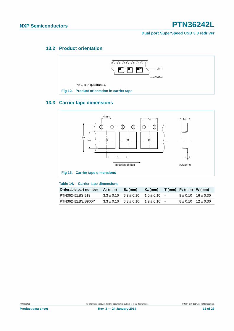
13.2 Product orientation
13.3 Carrier tape dimensions
Pin 1 is in quadrant 1.
Fig 12. Product orientation in carrier tape
Fig 13. Carrier tape dimensions
Table 14. Carrier tape dimensions
Orderable part number A0 (mm) B0 (mm) K0 (mm) T (mm) P1 (mm) W (mm)
PTN36242LBS,518 3.3 0.10 6.3 0.10 1.0 0.10 - 8 0.10 16 0.30
PTN36242LBS/S900Y 3.3 0.10 6.3 0.10 1.2 0.10 - 8 0.10 12 0.30
PTN36242L All information provided in this document is subject to legal disclaimers. © NXP B.V. 2014. All rights reserved.
Product data sheet Rev. 3 — 24 January 2014 18 of 26

NXP Semiconductors PTN36242LDual port SuperSpeed USB 3.0 redriver
13.4 Reel dimensions
Fig 14. Schematic view of reel
Table 15. Reel dimensions
Orderable part number A [nom](mm)
W2 [max](mm)
B [min](mm)
C [min](mm)
D [min](mm)
PTN36242LBS,518 330 22.4 1.5 12.8 20.2
PTN36242LBS/S900Y 330 14.5 1.5 12.8 20.2
PTN36242L All information provided in this document is subject to legal disclaimers. © NXP B.V. 2014. All rights reserved.
Product data sheet Rev. 3 — 24 January 2014 19 of 26

NXP Semiconductors PTN36242LDual port SuperSpeed USB 3.0 redriver
13.5 Barcode label
14. Soldering of SMD packages
This text provides a very brief insight into a complex technology. A more in-depth account of soldering ICs can be found in Application Note AN10365 “Surface mount reflow soldering description”.
14.1 Introduction to soldering
Soldering is one of the most common methods through which packages are attached to Printed Circuit Boards (PCBs), to form electrical circuits. The soldered joint provides both the mechanical and the electrical connection. There is no single soldering method that is ideal for all IC packages. Wave soldering is often preferred when through-hole and Surface Mount Devices (SMDs) are mixed on one printed wiring board; however, it is not suitable for fine pitch SMDs. Reflow soldering is ideal for the small pitches and high densities that come with increased miniaturization.
14.2 Wave and reflow soldering
Wave soldering is a joining technology in which the joints are made by solder coming from a standing wave of liquid solder. The wave soldering process is suitable for the following:
• Through-hole components
• Leaded or leadless SMDs, which are glued to the surface of the printed circuit board
Fig 15. Box and reel information barcode
Table 16. Barcode dimensions
Box barcode labell w (mm)
Reel barcode labell w (mm)
100 75 100 75
PTN36242L All information provided in this document is subject to legal disclaimers. © NXP B.V. 2014. All rights reserved.
Product data sheet Rev. 3 — 24 January 2014 20 of 26
NXP Semiconductors PTN36242LDual port SuperSpeed USB 3.0 redriver
Not all SMDs can be wave soldered. Packages with solder balls, and some leadless packages which have solder lands underneath the body, cannot be wave soldered. Also, leaded SMDs with leads having a pitch smaller than ~0.6 mm cannot be wave soldered, due to an increased probability of bridging.
The reflow soldering process involves applying solder paste to a board, followed by component placement and exposure to a temperature profile. Leaded packages, packages with solder balls, and leadless packages are all reflow solderable.
Key characteristics in both wave and reflow soldering are:
• Board specifications, including the board finish, solder masks and vias
• Package footprints, including solder thieves and orientation
• The moisture sensitivity level of the packages
• Package placement
• Inspection and repair
• Lead-free soldering versus SnPb soldering
14.3 Wave soldering
Key characteristics in wave soldering are:
• Process issues, such as application of adhesive and flux, clinching of leads, board transport, the solder wave parameters, and the time during which components are exposed to the wave
• Solder bath specifications, including temperature and impurities
14.4 Reflow soldering
Key characteristics in reflow soldering are:
• Lead-free versus SnPb soldering; note that a lead-free reflow process usually leads to higher minimum peak temperatures (see Figure 16) than a SnPb process, thus reducing the process window
• Solder paste printing issues including smearing, release, and adjusting the process window for a mix of large and small components on one board
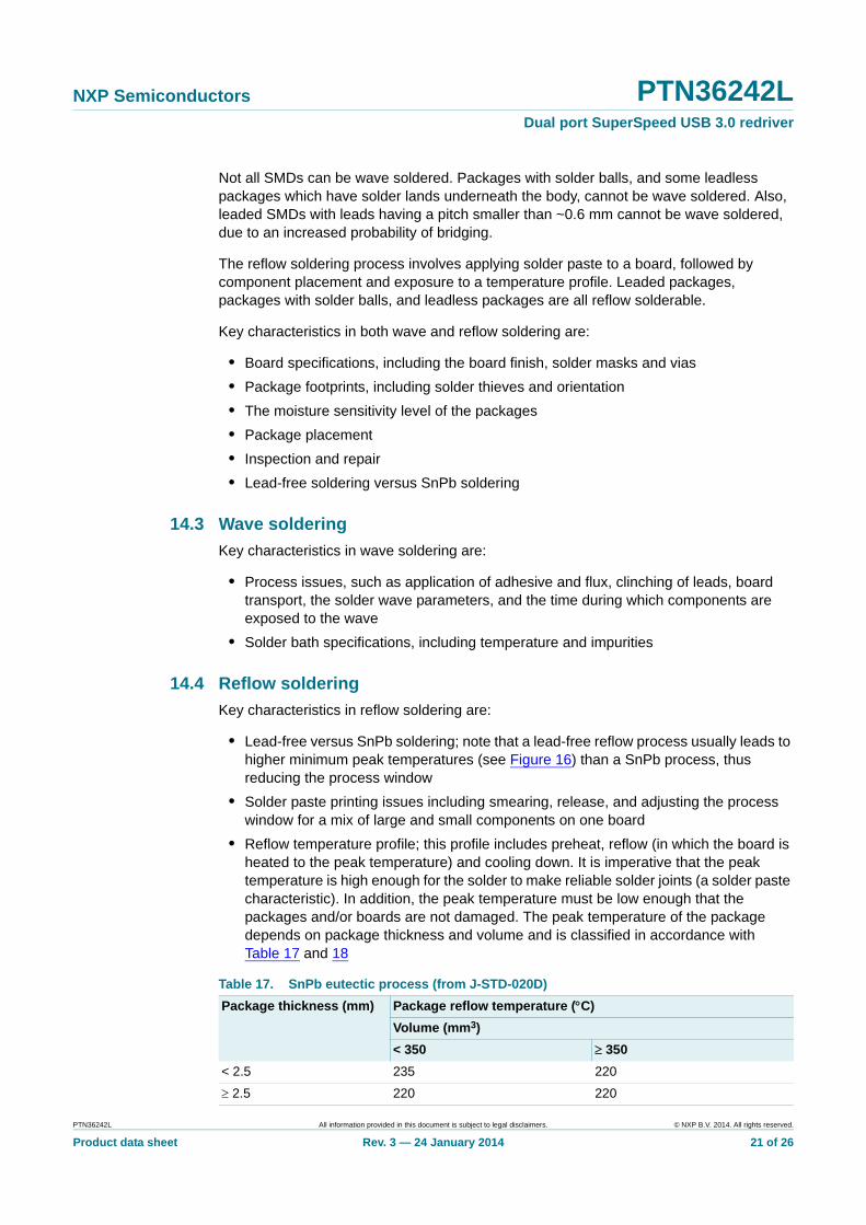
• Reflow temperature profile; this profile includes preheat, reflow (in which the board is heated to the peak temperature) and cooling down. It is imperative that the peak temperature is high enough for the solder to make reliable solder joints (a solder paste characteristic). In addition, the peak temperature must be low enough that the packages and/or boards are not damaged. The peak temperature of the package depends on package thickness and volume and is classified in accordance with Table 17 and 18
Table 17. SnPb eutectic process (from J-STD-020D)
Package thickness (mm) Package reflow temperature (C)
Volume (mm3)
< 350 350
< 2.5 235 220
2.5 220 220
PTN36242L All information provided in this document is subject to legal disclaimers. © NXP B.V. 2014. All rights reserved.
Product data sheet Rev. 3 — 24 January 2014 21 of 26

NXP Semiconductors PTN36242LDual port SuperSpeed USB 3.0 redriver
Moisture sensitivity precautions, as indicated on the packing, must be respected at all times.
Studies have shown that small packages reach higher temperatures during reflow soldering, see Figure 16.
For further information on temperature profiles, refer to Application Note AN10365 “Surface mount reflow soldering description”.
Table 18. Lead-free process (from J-STD-020D)
Package thickness (mm) Package reflow temperature (C)
Volume (mm3)
< 350 350 to 2000 > 2000
< 1.6 260 260 260
1.6 to 2.5 260 250 245
> 2.5 250 245 245
MSL: Moisture Sensitivity Level
Fig 16. Temperature profiles for large and small components
001aac844
temperature
time
minimum peak temperature= minimum soldering temperature
maximum peak temperature= MSL limit, damage level
peak temperature
PTN36242L All information provided in this document is subject to legal disclaimers. © NXP B.V. 2014. All rights reserved.
Product data sheet Rev. 3 — 24 January 2014 22 of 26

NXP Semiconductors PTN36242LDual port SuperSpeed USB 3.0 redriver
15. Abbreviations
16. Revision history
Table 19. Abbreviations
Acronym Description
AIO All In One computer platform
CDM Charged-Device Model
HBM Human Body Model
I2C-bus Inter-Integrated Circuit bus
IC Integrated Circuit
LFPS Low Frequency Periodic Sampling
PCB Printed-Circuit Board
Rx Receive
SI Signal Integrity
Tx Transmit
USB Universal Serial Bus
Table 20. Revision history
Document ID Release date Data sheet status Change notice Supersedes
PTN36242L v.3 20140124 Product data sheet - PTN36242L v.2
Modifications: • Table 1 “Ordering information”:
– added Type number PTN36242LBS/S900
• Table 2 “Ordering options”:
– added Table note [1] and its reference at PTN36242LBS packing method
– added Table note [2] and its reference at PTN36242LBS/S900 packing method
• Added Section 13 “Packing information”
PTN36242L v.2 20130619 Product data sheet - PTN36242L v.1
PTN36242L v.1 20130411 Product data sheet - -
PTN36242L All information provided in this document is subject to legal disclaimers. © NXP B.V. 2014. All rights reserved.
Product data sheet Rev. 3 — 24 January 2014 23 of 26

NXP Semiconductors PTN36242LDual port SuperSpeed USB 3.0 redriver
17. Legal information
17.1 Data sheet status
[1] Please consult the most recently issued document before initiating or completing a design.
[2] The term ‘short data sheet’ is explained in section “Definitions”.
[3] The product status of device(s) described in this document may have changed since this document was published and may differ in case of multiple devices. The latest product status information is available on the Internet at URL http://www.nxp.com.
17.2 Definitions
Draft — The document is a draft version only. The content is still under internal review and subject to formal approval, which may result in modifications or additions. NXP Semiconductors does not give any representations or warranties as to the accuracy or completeness of information included herein and shall have no liability for the consequences of use of such information.
Short data sheet — A short data sheet is an extract from a full data sheet with the same product type number(s) and title. A short data sheet is intended for quick reference only and should not be relied upon to contain detailed and full information. For detailed and full information see the relevant full data sheet, which is available on request via the local NXP Semiconductors sales office. In case of any inconsistency or conflict with the short data sheet, the full data sheet shall prevail.
Product specification — The information and data provided in a Product data sheet shall define the specification of the product as agreed between NXP Semiconductors and its customer, unless NXP Semiconductors and customer have explicitly agreed otherwise in writing. In no event however, shall an agreement be valid in which the NXP Semiconductors product is deemed to offer functions and qualities beyond those described in the Product data sheet.
17.3 Disclaimers
Limited warranty and liability — Information in this document is believed to be accurate and reliable. However, NXP Semiconductors does not give any representations or warranties, expressed or implied, as to the accuracy or completeness of such information and shall have no liability for the consequences of use of such information. NXP Semiconductors takes no responsibility for the content in this document if provided by an information source outside of NXP Semiconductors.
In no event shall NXP Semiconductors be liable for any indirect, incidental, punitive, special or consequential damages (including - without limitation - lost profits, lost savings, business interruption, costs related to the removal or replacement of any products or rework charges) whether or not such damages are based on tort (including negligence), warranty, breach of contract or any other legal theory.
Notwithstanding any damages that customer might incur for any reason whatsoever, NXP Semiconductors’ aggregate and cumulative liability towards customer for the products described herein shall be limited in accordance with the Terms and conditions of commercial sale of NXP Semiconductors.
Right to make changes — NXP Semiconductors reserves the right to make changes to information published in this document, including without limitation specifications and product descriptions, at any time and without notice. This document supersedes and replaces all information supplied prior to the publication hereof.
Suitability for use — NXP Semiconductors products are not designed, authorized or warranted to be suitable for use in life support, life-critical or safety-critical systems or equipment, nor in applications where failure or malfunction of an NXP Semiconductors product can reasonably be expected to result in personal injury, death or severe property or environmental damage. NXP Semiconductors and its suppliers accept no liability for inclusion and/or use of NXP Semiconductors products in such equipment or applications and therefore such inclusion and/or use is at the customer’s own risk.
Applications — Applications that are described herein for any of these products are for illustrative purposes only. NXP Semiconductors makes no representation or warranty that such applications will be suitable for the specified use without further testing or modification.
Customers are responsible for the design and operation of their applications and products using NXP Semiconductors products, and NXP Semiconductors accepts no liability for any assistance with applications or customer product design. It is customer’s sole responsibility to determine whether the NXP Semiconductors product is suitable and fit for the customer’s applications and products planned, as well as for the planned application and use of customer’s third party customer(s). Customers should provide appropriate design and operating safeguards to minimize the risks associated with their applications and products.
NXP Semiconductors does not accept any liability related to any default, damage, costs or problem which is based on any weakness or default in the customer’s applications or products, or the application or use by customer’s third party customer(s). Customer is responsible for doing all necessary testing for the customer’s applications and products using NXP Semiconductors products in order to avoid a default of the applications and the products or of the application or use by customer’s third party customer(s). NXP does not accept any liability in this respect.
Limiting values — Stress above one or more limiting values (as defined in the Absolute Maximum Ratings System of IEC 60134) will cause permanent damage to the device. Limiting values are stress ratings only and (proper) operation of the device at these or any other conditions above those given in the Recommended operating conditions section (if present) or the Characteristics sections of this document is not warranted. Constant or repeated exposure to limiting values will permanently and irreversibly affect the quality and reliability of the device.
Terms and conditions of commercial sale — NXP Semiconductors products are sold subject to the general terms and conditions of commercial sale, as published at http://www.nxp.com/profile/terms, unless otherwise agreed in a valid written individual agreement. In case an individual agreement is concluded only the terms and conditions of the respective agreement shall apply. NXP Semiconductors hereby expressly objects to applying the customer’s general terms and conditions with regard to the purchase of NXP Semiconductors products by customer.
No offer to sell or license — Nothing in this document may be interpreted or construed as an offer to sell products that is open for acceptance or the grant, conveyance or implication of any license under any copyrights, patents or other industrial or intellectual property rights.
Document status[1][2] Product status[3] Definition
Objective [short] data sheet Development This document contains data from the objective specification for product development.
Preliminary [short] data sheet Qualification This document contains data from the preliminary specification.
Product [short] data sheet Production This document contains the product specification.
PTN36242L All information provided in this document is subject to legal disclaimers. © NXP B.V. 2014. All rights reserved.
Product data sheet Rev. 3 — 24 January 2014 24 of 26

NXP Semiconductors PTN36242LDual port SuperSpeed USB 3.0 redriver
Export control — This document as well as the item(s) described herein may be subject to export control regulations. Export might require a prior authorization from competent authorities.
Non-automotive qualified products — Unless this data sheet expressly states that this specific NXP Semiconductors product is automotive qualified, the product is not suitable for automotive use. It is neither qualified nor tested in accordance with automotive testing or application requirements. NXP Semiconductors accepts no liability for inclusion and/or use of non-automotive qualified products in automotive equipment or applications.
In the event that customer uses the product for design-in and use in automotive applications to automotive specifications and standards, customer (a) shall use the product without NXP Semiconductors’ warranty of the product for such automotive applications, use and specifications, and (b) whenever customer uses the product for automotive applications beyond
NXP Semiconductors’ specifications such use shall be solely at customer’s own risk, and (c) customer fully indemnifies NXP Semiconductors for any liability, damages or failed product claims resulting from customer design and use of the product for automotive applications beyond NXP Semiconductors’ standard warranty and NXP Semiconductors’ product specifications.
Translations — A non-English (translated) version of a document is for reference only. The English version shall prevail in case of any discrepancy between the translated and English versions.
17.4 TrademarksNotice: All referenced brands, product names, service names and trademarks are the property of their respective owners.
18. Contact information
For more information, please visit: http://www.nxp.com
For sales office addresses, please send an email to: [email protected]
PTN36242L All information provided in this document is subject to legal disclaimers. © NXP B.V. 2014. All rights reserved.
Product data sheet Rev. 3 — 24 January 2014 25 of 26

NXP Semiconductors PTN36242LDual port SuperSpeed USB 3.0 redriver
19. Contents
1 General description . . . . . . . . . . . . . . . . . . . . . . 1
2 Features and benefits . . . . . . . . . . . . . . . . . . . . 1
3 Applications . . . . . . . . . . . . . . . . . . . . . . . . . . . . 2
4 System context diagrams . . . . . . . . . . . . . . . . . 3
5 Ordering information. . . . . . . . . . . . . . . . . . . . . 45.1 Ordering options . . . . . . . . . . . . . . . . . . . . . . . . 4
6 Block diagram . . . . . . . . . . . . . . . . . . . . . . . . . . 5
7 Pinning information. . . . . . . . . . . . . . . . . . . . . . 67.1 Pinning . . . . . . . . . . . . . . . . . . . . . . . . . . . . . . . 67.2 Pin description . . . . . . . . . . . . . . . . . . . . . . . . . 6
8 Functional description . . . . . . . . . . . . . . . . . . . 98.1 Receive equalization . . . . . . . . . . . . . . . . . . . . 98.2 Transmit de-emphasis . . . . . . . . . . . . . . . . . . . 98.3 Device states and power management . . . . . 10
9 Limiting values. . . . . . . . . . . . . . . . . . . . . . . . . 11
10 Recommended operating conditions. . . . . . . 11
11 Characteristics. . . . . . . . . . . . . . . . . . . . . . . . . 1211.1 Device characteristics. . . . . . . . . . . . . . . . . . . 1211.2 Receiver AC/DC characteristics . . . . . . . . . . . 1311.3 Transmitter AC/DC characteristics . . . . . . . . . 1411.4 Jitter performance. . . . . . . . . . . . . . . . . . . . . . 1511.5 Control inputs . . . . . . . . . . . . . . . . . . . . . . . . . 15
12 Package outline . . . . . . . . . . . . . . . . . . . . . . . . 16
13 Packing information . . . . . . . . . . . . . . . . . . . . 1713.1 Packing method . . . . . . . . . . . . . . . . . . . . . . . 1713.2 Product orientation . . . . . . . . . . . . . . . . . . . . . 1813.3 Carrier tape dimensions . . . . . . . . . . . . . . . . . 1813.4 Reel dimensions . . . . . . . . . . . . . . . . . . . . . . . 1913.5 Barcode label . . . . . . . . . . . . . . . . . . . . . . . . . 20
14 Soldering of SMD packages . . . . . . . . . . . . . . 2014.1 Introduction to soldering . . . . . . . . . . . . . . . . . 2014.2 Wave and reflow soldering . . . . . . . . . . . . . . . 2014.3 Wave soldering . . . . . . . . . . . . . . . . . . . . . . . . 2114.4 Reflow soldering . . . . . . . . . . . . . . . . . . . . . . . 21
15 Abbreviations. . . . . . . . . . . . . . . . . . . . . . . . . . 23
16 Revision history. . . . . . . . . . . . . . . . . . . . . . . . 23
17 Legal information. . . . . . . . . . . . . . . . . . . . . . . 2417.1 Data sheet status . . . . . . . . . . . . . . . . . . . . . . 2417.2 Definitions. . . . . . . . . . . . . . . . . . . . . . . . . . . . 2417.3 Disclaimers . . . . . . . . . . . . . . . . . . . . . . . . . . . 2417.4 Trademarks. . . . . . . . . . . . . . . . . . . . . . . . . . . 25
18 Contact information. . . . . . . . . . . . . . . . . . . . . 25
19 Contents . . . . . . . . . . . . . . . . . . . . . . . . . . . . . . 26
© NXP B.V. 2014. All rights reserved.
For more information, please visit: http://www.nxp.comFor sales office addresses, please send an email to: [email protected]
Date of release: 24 January 2014
Document identifier: PTN36242L
Please be aware that important notices concerning this document and the product(s)described herein, have been included in section ‘Legal information’.