
SN75LVCP601 Two-Channel 6-Gbps SATA Redriver datasheet ...
35
ICH R HDD eSATA Cable eSATA connector PC/WS MB R = SN75LVCP601 ICH R Notebook Dock Dock Connector PC/Workstation Motherboard Notebook Dock HDD eSATA Cable (2m) eSATA connector SATA 6G Host HDD DT MB Desktop Main Board iSATA connector R Product Folder Sample & Buy Technical Documents Tools & Software Support & Community An IMPORTANT NOTICE at the end of this data sheet addresses availability, warranty, changes, use in safety-critical applications, intellectual property matters and other important disclaimers. PRODUCTION DATA. SN75LVCP601 SLLSE41H – JUNE 2010 – REVISED MARCH 2016 SN75LVCP601 Two-Channel 6-Gbps SATA Redriver 1 1 Features 1• 1.5-, 3-, or 6-Gbps Two-Channel Redriver • Integrated Output Squelch • Programmable RX and TX Equalization and De-Emphasis Width Control • Power-Save Feature Lowers Power by >80% in Auto Low-Power Mode • Low Power – <220 mW (Typ) – <50 mW (in Auto Low-Power Mode) – <5 mW (in Standby Mode) • Excellent Jitter and Loss Compensation Capability to Over 24-Inch (61-cm) FR4 Trace • 20-Pin 4-mm × 4-mm QFN Package • High Protection Against ESD Transient – HBM: 10,000 V – CDM: 1,500 V – MM: 200 V • Pin-Compatible With LVCP412A and MAX4951 2 Applications • Notebooks • Desktops • Docking Stations • Servers • Workstations 3 Description The SN75LVCP601 device is a dual-channel, single- lane SATA redriver and signal conditioner supporting data rates up to 6 Gbps. The device complies with SATA physical link 2m and 3i specifications. The SN75LVCP601 operates from one 3.3-V supply and has 100-Ω line termination with a self-biasing feature, making the device suitable for ac coupling. The inputs incorporate an out-of-band (OOB) detector, which automatically squelches the output while maintaining a stable common-mode voltage compliant to the SATA link. The device design also handles spread- spectrum clocking (SSC) transmission per the SATA specification. The SN75LVCP601 device handles interconnect losses at both its input and output. The input stage of each channel offers selectable equalization settings that are programmable to match the loss in the channel. The differential outputs provide selectable de-emphasis to compensate for the expected distortion that the SATA signal experiences. The level of equalization and de-emphasis settings depends on the length of interconnect and its characteristics. The setting of signal control pins EQ1, EQ2, DE1, and DE2 controls both equalization and de-emphasis levels. This device is hot-plug capable (requires the use of ac-coupling capacitors at differential inputs and outputs), thus preventing device damage under device hot-insertion, in such cases as: async signal plug or removal, unpowered plug or removal, powered plug or removal, surprise plug or removal Device Information (1) PART NUMBER PACKAGE BODY SIZE (NOM) SN75LVCP601 WQFN (20) 4.00 mm × 4.00 mm (1) For all available packages, see the orderable addendum at the end of the data sheet. Typical Application
Transcript of SN75LVCP601 Two-Channel 6-Gbps SATA Redriver datasheet ...

ICH
R
HDD
eSATA
Cable
eSATA
connector
PC/WS MB
R = SN75LVCP601
ICH
R
Notebook Dock
Dock
Co
nnecto
r
PC/Workstation
Motherboard Notebook Dock
HDD
eSATA Cable
(2m)
eSATA
connectorSATA 6G Host
HDD
DT MB
Desktop Main Board
iSATA
connector
R
Product
Folder
Sample &Buy
Technical
Documents
Tools &
Software
Support &Community
An IMPORTANT NOTICE at the end of this data sheet addresses availability, warranty, changes, use in safety-critical applications,intellectual property matters and other important disclaimers. PRODUCTION DATA.
SN75LVCP601SLLSE41H –JUNE 2010–REVISED MARCH 2016
SN75LVCP601 Two-Channel 6-Gbps SATA Redriver
1
1 Features1• 1.5-, 3-, or 6-Gbps Two-Channel Redriver• Integrated Output Squelch• Programmable RX and TX Equalization and
De-Emphasis Width Control• Power-Save Feature Lowers Power by >80%
in Auto Low-Power Mode• Low Power
– <220 mW (Typ)– <50 mW (in Auto Low-Power Mode)– <5 mW (in Standby Mode)
• Excellent Jitter and Loss CompensationCapability to Over 24-Inch (61-cm) FR4 Trace
• 20-Pin 4-mm × 4-mm QFN Package• High Protection Against ESD Transient
– HBM: 10,000 V– CDM: 1,500 V– MM: 200 V
• Pin-Compatible With LVCP412A and MAX4951
2 Applications• Notebooks• Desktops• Docking Stations• Servers• Workstations
3 DescriptionThe SN75LVCP601 device is a dual-channel, single-lane SATA redriver and signal conditioner supportingdata rates up to 6 Gbps. The device complies withSATA physical link 2m and 3i specifications. TheSN75LVCP601 operates from one 3.3-V supply andhas 100-Ω line termination with a self-biasing feature,making the device suitable for ac coupling. The inputsincorporate an out-of-band (OOB) detector, whichautomatically squelches the output while maintaininga stable common-mode voltage compliant to theSATA link. The device design also handles spread-spectrum clocking (SSC) transmission per the SATAspecification.
The SN75LVCP601 device handles interconnectlosses at both its input and output. The input stage ofeach channel offers selectable equalization settingsthat are programmable to match the loss in thechannel. The differential outputs provide selectablede-emphasis to compensate for the expecteddistortion that the SATA signal experiences. The levelof equalization and de-emphasis settings depends onthe length of interconnect and its characteristics. Thesetting of signal control pins EQ1, EQ2, DE1, andDE2 controls both equalization and de-emphasislevels.
This device is hot-plug capable (requires the use ofac-coupling capacitors at differential inputs andoutputs), thus preventing device damage underdevice hot-insertion, in such cases as: async signalplug or removal, unpowered plug or removal,powered plug or removal, surprise plug or removal
Device Information(1)
PART NUMBER PACKAGE BODY SIZE (NOM)SN75LVCP601 WQFN (20) 4.00 mm × 4.00 mm
(1) For all available packages, see the orderable addendum atthe end of the data sheet.
Typical Application

2
SN75LVCP601SLLSE41H –JUNE 2010–REVISED MARCH 2016 www.ti.com
Product Folder Links: SN75LVCP601
Submit Documentation Feedback Copyright © 2010–2016, Texas Instruments Incorporated
Table of Contents1 Features .................................................................. 12 Applications ........................................................... 13 Description ............................................................. 14 Revision History..................................................... 25 Pin Configuration and Functions ......................... 46 Specifications......................................................... 5
6.1 Absolute Maximum Ratings ...................................... 56.2 ESD Ratings.............................................................. 56.3 Recommended Operating Conditions....................... 56.4 Thermal Information .................................................. 56.5 Electrical Characteristics........................................... 66.6 Power Dissipation Characteristics ............................ 76.7 Timing Requirements ................................................ 86.8 Switching Characteristics .......................................... 86.9 Typical Characteristics ............................................ 10
7 Parameter Measurement Information ................ 117.1 Jitter and VOD Results: Case 1 at 6 Gbps ............. 127.2 Jitter and VOD Results: Case 2 at 3 Gbps ............. 137.3 Jitter and VOD Results: Case 3 at 1.5 Gbps .......... 15
8 Detailed Description ............................................ 178.1 Overview ................................................................. 178.2 Functional Block Diagram ....................................... 178.3 Feature Description................................................. 188.4 Device Functional Modes........................................ 18
9 Application and Implementation ........................ 199.1 Application Information............................................ 199.2 Typical Application ................................................. 19
10 Power Supply Recommendations ..................... 2511 Layout................................................................... 25
11.1 Layout Guidelines ................................................. 2511.2 Layout Example .................................................... 26
12 Device and Documentation Support ................. 2712.1 Community Resources.......................................... 2712.2 Trademarks ........................................................... 2712.3 Electrostatic Discharge Caution............................ 2712.4 Glossary ................................................................ 27
13 Mechanical, Packaging, and OrderableInformation ........................................................... 27
4 Revision HistoryNOTE: Page numbers for previous revisions may differ from page numbers in the current version.
Changes from Revision G (January 2016) to Revision H Page
• Changed pin DE1 number From: 8 To: 9 in the Pin Functions table .................................................................................... 4• Changed pin DE2 number From: 9 To: 8 in the Pin Functions table .................................................................................... 4
Changes from Revision F (June 2015) to Revision G Page
• Changed Pin 8 name To: DE2 and Pin 9 name To: DE1 in Figure 27 ............................................................................... 20
Changes from Revision E (January 2014) to Revision F Page
• Added Pin Configuration and Functions section, ESD Ratings table, Feature Description section, Device FunctionalModes, Application and Implementation section, Power Supply Recommendations section, Layout section, Deviceand Documentation Support section, and Mechanical, Packaging, and Orderable Information section .............................. 1
• Added Storage temperature to the Absolute Maximum Ratings table ................................................................................... 5• Moved timing parameters out of Electrical Characteristics and into Timing Requirements .................................................. 8• Moved switching parameters out of Electrical Characteristics and into Switching Characteristics ....................................... 8
Changes from Revision D (January 2013) to Revision E Page
• Changed DJTX (UI = 333 ps) From: Max = 0.19 To: Max = 0.07 ........................................................................................... 8• Changed DJTX (UI = 167 ps) From: Max = 0.34 To: Max = 0.16 ........................................................................................... 8
Changes from Revision C (October 2012) to Revision D Page
• Corrected formatting of the Differential output-voltage swing dc level section of the Electrical Characteristics table ........... 7

3
SN75LVCP601www.ti.com SLLSE41H –JUNE 2010–REVISED MARCH 2016
Product Folder Links: SN75LVCP601
Submit Documentation FeedbackCopyright © 2010–2016, Texas Instruments Incorporated
Changes from Revision B (February 2012) to Revision C Page
• Deleted DiffVppTX row............................................................................................................................................................... 7• Inserted DiffVppTX_DE row ......................................................................................................................................................... 7• Changed Figure 5 caption .................................................................................................................................................... 10• Revised text of the Output Ed-Emphasis section ................................................................................................................. 18• Deleted setting recommendations on pulse durations for DEW1 and DEW2 ...................................................................... 18
Changes from Revision A (October 2011) to Revision B Page
• Changed pin type from CML to VML for pins 4, 5, 14, 15 in the Pin Functions table ............................................................ 4
Changes from Original (June 2010) to Revision A Page
• Changed pin EN number From: 4 To: 7 in the Pin Functions table ....................................................................................... 4

20
19
18
17
16
6
7
8
9
10
15
14
13
12
11
1 2 3 4 5
RX
1P
RX
1N
GN
D
TX
2N
TX
2P
VCC
EN
DE 2
DE 1
DEW 2
RX
2P
RX
2N
GN
D
TX
1N
TX
1P
EQ 2
EQ 1
VCC
DEW 1
GND
LVCP601RTJ
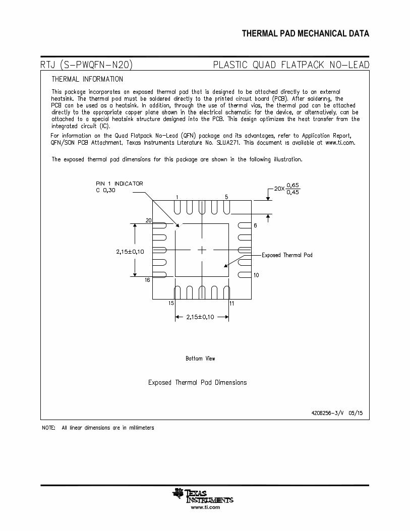
Thermal Pad must
be soldered to PCB
GND plane for
efficient thermal
performance
Bottom View
1 1 1
2
1
RX
1P
RX
1N
GN
D
TX
2N
TX
2P
DEW 2
DE 1
DE 2
EN
VCC
RX
2P
RX
2N
GN
D
TX
1N
TX
1P
VCC
DEW 1
EQ 2
EQ 1
GND LVCP601RTJ
Top View
18
19
20
10
9
8
7
6
1 2 3 4 5
16
17
11
12
13
14
15
4
SN75LVCP601SLLSE41H –JUNE 2010–REVISED MARCH 2016 www.ti.com
Product Folder Links: SN75LVCP601
Submit Documentation Feedback Copyright © 2010–2016, Texas Instruments Incorporated
(1) Internally biased to VCC / 2 with >200-kΩ pullup or pulldown. When 3-state pins are left as NC, board leakage at the pin pad must be<1 µA; otherwise, drive to VCC / 2 to assert mid-level state.
5 Pin Configuration and Functions
RTJ Package16-Pin WQFN With Thermal Pad
Pin FunctionsPIN
PIN TYPE DESCRIPTIONNAME NO.
CONTROL PINSDE1 (1) 9
I, LVCMOS Selects de-emphasis settings for CH 1 and CH 2 per Table 1.Internally tied to VCC / 2.DE2 (1) 8
DEW1 16I, LVCMOS
De-emphasis width control for CH 1 and CH 2.0 = De-emphasis pulse duration, short1 = De-emphasis pulse duration, long (default)DEW2 6
EN 7 I, LVCMOSDevice enable and disable pin, internally pulled to VCC.0 = Device in standby mode1 = Device enabled (default)
EQ1 (1) 17I, LVCMOS Selects equalization settings for CH 1 and CH 2 per Table 1.
Internally tied to VCC / 2.EQ2 (1) 19HIGH-SPEED DIFFERENTIAL I/ORX1N 2 I, CML
Noninverting and inverting CML differential input for CH 1 and CH 2. These pinsconnect to an internal voltage bias via a dual-termination resistor circuit.
RX1P 1 I, CMLRX2N 12 I, CMLRX2P 11 I, CMLTX1N 14 O, VML
Noninverting and inverting VML differential output for CH 1 and CH 2. These pinsconnect internally to voltage bias via termination resistors.
TX1P 15 O, VMLTX2N 4 O, VMLTX2P 5 O, VMLPOWERGND 3, 13, 18 Power Supply groundVCC 10, 20 Power Positive supply must be 3.3 V ± 10%

5
SN75LVCP601www.ti.com SLLSE41H –JUNE 2010–REVISED MARCH 2016
Product Folder Links: SN75LVCP601
Submit Documentation FeedbackCopyright © 2010–2016, Texas Instruments Incorporated
(1) Stresses beyond those listed under Absolute Maximum Ratings may cause permanent damage to the device. These are stress ratingsonly, and functional operation of the device at these or any conditions beyond those indicated under Recommended OperatingConditions is not implied. Exposure to absolute-maximum-rated conditions for extended periods may affect device reliability.
(2) All voltage values, except differential voltages, are with respect to the network ground terminal.
6 Specifications
6.1 Absolute Maximum Ratingsover operating free-air temperature range (unless otherwise noted) (1)
MIN MAX UNITVCC Supply voltage range (2) –0.5 4 V
Voltage rangeDifferential I/O –0.5 4 VControl I/O –0.5 VCC + 0.5 V
Continuous power dissipation See Power DissipationCharacteristics
Tstg Storage temperature 150 °C
(1) JEDEC document JEP155 states that 500-V HBM allows safe manufacturing with a standard ESD control process.(2) JEDEC document JEP157 states that 250-V CDM allows safe manufacturing with a standard ESD control process.(3) Tested in accordance with JEDEC Standard 22, Test Method A115-A.
6.2 ESD RatingsVALUE UNIT
V(ESD) Electrostatic discharge
Human body model (HBM), per ANSI/ESDA/JEDEC JS-001 (1) ±10000
VCharged-device model (CDM), per JEDEC specification JESD22-C101 (2) ±1500
Machine model (3) ±200
6.3 Recommended Operating Conditionstypical values for all parameters are VCC = 3.3 V and TA = 25°C; all temperature limits are specified by design
MIN NOM MAX UNITVCC Supply voltage 3 3.3 3.6 VCCOUPLING Coupling capacitor 12 nF
Operating free-air temperature 0 85 °C
(1) For more information about traditional and new thermal metrics, see the Semiconductor and IC Package Thermal Metrics applicationreport, SPRA953.
6.4 Thermal Information
THERMAL METRIC (1)SN75LVCP601
UNITRTJ (WQFN)20 PINS
RθJA Junction-to-ambient thermal resistance 38 °C/WRθJC(top) Junction-to-case (top) thermal resistance 40 °C/WRθJB Junction-to-board thermal resistance 10 °C/WψJT Junction-to-top characterization parameter 0.5 °C/WψJB Junction-to-board characterization parameter 0.9 °C/WRθJC(bot) Junction-to-case (bottom) thermal resistance 15.2 °C/W

6
SN75LVCP601SLLSE41H –JUNE 2010–REVISED MARCH 2016 www.ti.com
Product Folder Links: SN75LVCP601
Submit Documentation Feedback Copyright © 2010–2016, Texas Instruments Incorporated
6.5 Electrical Characteristicsover operating free-air temperature range (unless otherwise noted)
PARAMETER TEST CONDITIONS MIN TYP MAX UNITDEVICE PARAMETERS
PD Power dissipation in active mode DEWx = EN = VCC, EQx = DEx = NC, K28.5pattern at 6 Gbps, VID = 700 mVp-p
215 288 mW
PSDPower dissipation in standbymode
EN = 0 V, DEWx = EQx = DEx = NC, K28.5pattern at 6 Gbps, VID = 700 mVp-p
5 mW
ICC Active-mode supply current EN = 3.3 V, DEWx = 0 V, EQx = DEx = NC,K28.5 pattern at 6 Gbps, VID = 700 mVp-p
65 80 mA
ICC_ALP Acive power-save mode ICCWhen device is enabled and auto low-powerconditions are met 6.5 10 mA
ICC_STDBY Standby mode supply current EN = 0 V 1 mAMaximum data rate 1 6 Gbps
OUT-OF-BAND (OOB)VOOB Input OOB threshold f = 750 MHz 50 78 150 mVppDVdiffOOB OOB differential delta 25 mVDVCMOOB OOB common-mode delta 50 mVCONTROL LOGICVIH Input high voltage For all control pins 1.4 VVIL Input low voltage 0.5 VVINHYS Input hysteresis 115 mV
IIH High-level input currentEQx, DEx = VCC 30
µAEN, DEWx = VCC 1
IIL Low-level input currentEQx, DEx = GND –30
µAEN, DEWx = GND –10
RECEIVER AC/DCZDIFFRX Differential-input impedance 85 100 115 ΩZSERX Single-ended input impedance 40 ΩVCMRX Common-mode voltage 1.8 V
RLDiffRX Differential-mode return loss (RL)
f = 150 MHz to 300 MHz 18 28
dBf = 300 MHz to 600 MHz 14 17f = 600 MHz to 1.2 GHz 10 12f = 1.2 GHz to 2.4 GHz 8 9f = 2.4 GHz to 3 GHz 3 9
RXDiffRLSlope Differential-mode RL slope f = 300 MHz to 6 GHz (see Figure 1) –13 dB/dec
RLCMRX Common-mode return loss
f = 150 MHz to 300 MHz 5 10
dBf = 300 MHz to 600 MHz 5 17f = 600 MHz to 1.2 GHz 2 23f = 1.2 GHz to 2.4 GHz 1 16f = 2.4 GHz to 3 GHz 1 12
VdiffRX Differential input voltage PP f = 1.5 GHz and 3 GHz 120 1600 mVppd
IBRX Impedance balance
f = 150 MHz to 300 MHz 30 41
dB
f = 300 MHz to 600 MHz 30 38f = 600 MHz to 1.2 GHz 20 32f = 1.2 GHz to 2.4 GHz 10 26f = 2.4 GHz to 3 GHz 10 25f = 3 GHz to 5 GHz 4 20f = 5 GHz to 6.5 GHz 4 17

7
SN75LVCP601www.ti.com SLLSE41H –JUNE 2010–REVISED MARCH 2016
Product Folder Links: SN75LVCP601
Submit Documentation FeedbackCopyright © 2010–2016, Texas Instruments Incorporated
Electrical Characteristics (continued)over operating free-air temperature range (unless otherwise noted)
PARAMETER TEST CONDITIONS MIN TYP MAX UNITTRANSMITTER AC/DCZdiffTX Pair differential impedance 85 100 122 ΩZSETX Single-ended impedance 40 Ω
VTXtrans Sequencing transient voltage Transient voltages on the serial data busduring power sequencing (lab load) –1.2 1.2 V
RLDiffTX Differential-mode return loss
f = 150 MHz to 300 MHz 14 24
dBf = 300 MHz to 600 MHz 8 19f = 600 MHz to 1.2 GHz 6 14f = 1.2 GHz to 2.4 GHz 6 10f = 2.4 GHz to 3 GHz 3 10
TXDiffRLSlope Differential-mode RL slope f = 300 MHz to 3 GHz (see Figure 1) –13 dB/dec
RLCMTX Common-mode return loss
f = 150 MHz to 300 MHz 5 20
dBf = 300 MHz to 600 MHz 5 19f = 600 MHz to 1.2 GHz 2 17f = 1.2 GHz to 2.4 GHz 1 12f = 2.4 GHz to 3.0 GHz 1 11
IBTX Impedance balance
f = 150 MHz to 300 MHz 30 41
dB
f = 300 MHz to 600 MHz 30 38f = 600 MHz to 1.2 GHz 20 33f = 1.2 GHz to 2.4 GHz 10 24f = 2.4 GHz to 3 GHz 10 26f = 3 GHz to 5 GHz 4 22f = 5 GHz to 6.5 GHz 4 21
DE Output de-emphasis (relative totransition bit)
f = 3 GHz, DE1 or DE2 = 0 0dBf = 3 GHz, DE1 or DE2 = 1 –2
f = 3 GHz, DE1 or DE2 = NC –4
DiffVppTX_DEDifferential output-voltage swingdc level
f = 3 GHz, DE1 or DE2 = 0 550mVf = 3 GHz, DE1 or DE2 = 1 830
f = 3 GHz, DE1or DE2 = NC 630
VCMAC_TX TX AC CM voltageAt 1.5 GHz 20 50 mVppdAt 3 GHz 12 26 dBmV
(rms)At 6 GHz 13 30VCMTX Common-mode voltage 1.8 VTxR/FImb TX rise-fall imbalance At 3 Gbps 6% 20%TxAmpImb TX amplitude imbalance 2% 10%
6.6 Power Dissipation Characteristicsover operating free-air temperature range (unless otherwise noted)
PARAMETER MIN MAX UNITPD Device power dissipation in active mode 215 288 mWPSD Device power dissipation under standby mode 5 mW

8
SN75LVCP601SLLSE41H –JUNE 2010–REVISED MARCH 2016 www.ti.com
Product Folder Links: SN75LVCP601
Submit Documentation Feedback Copyright © 2010–2016, Texas Instruments Incorporated
6.7 Timing RequirementsMIN NOM MAX UNIT
DEVICE PARAMETERSAutoLPENTRY Auto low-power entry time Electrical idle at input (see Figure 4) 80 105 130 µsAutoLPEXIT Auto low-power exit time After first signal activity (see Figure 4) 42 50 nsTRANSMITTER AC/DC
tDE De-emphasis durationDEW1 or DEW2 = 0 94
psDEW1 or DEW2 = 1 215
OUT-OF-BAND (OOB)tOOB1 OOB mode enter See Figure 4 3 5 nstOOB2 OOB mode exit See Figure 4 3 5 ns
(1) TJ = (14.1 × RJSD + DJ), where RJSD is one standard deviation value of RJ Gaussian distribution. Jitter measurement is at the SATAconnector and includes jitter generated at the package connection on the printed circuit board, and at the board interconnect as shownin Figure 9.
6.8 Switching Characteristicsover operating free-air temperature range (unless otherwise noted)
PARAMETER TEST CONDITIONS MIN TYP MAX UNITDEVICE PARAMETERStPDelay Propagation delay Measured using K28.5 pattern (see Figure 2) 323 400 pstENB Device enable time EN 0 → 1 5 µstDIS Device disable time EN 1 → 0 2 µsRECEIVER AC/DC
t20-80RX Rise/fall timeRise times and fall times measured between 20%and 80% of the signal. SATA 6-Gbps speedmeasured 1 in, (2.5 cm) from device pin.
62 75 ps
tskewRX Differential skew
Difference between the single-ended midpoint ofthe RX+ signal rising or falling edge, and thesingle-ended midpoint of the RX– signal falling orrising edge.
30 ps
TRANSMITTER AC/DC
t20-80TX Rise/fall timeRise times and fall times measured between 20%and 80% of the signal. At 6 Gbps under no loadconditions.
42 55 75 ps
tskewTX Differential skew
Difference between the single-ended mid-point ofthe TX+ signal rising or falling edge, and thesingle-ended mid-point of the TX– signal falling orrising edge.
6 20 ps
TRANSMITTER JITTER
DJTXDeterministic jitter (1) at CP inFigure 9
VID = 500 mVpp, UI = 333 ps,K28.5 control character 0.06 0.07 UIp-p
RJTX Residual random jitter (1) VID = 500 mVpp, UI = 333 ps,K28.7 control character 0.01 2 ps-rms
DJTXDeterministic jitter (1) at CP inFigure 9
VID = 500 mVpp, UI = 167 ps,K28.5 control character 0.08 0.16 UIp-p
RJTX Residual random jitter (1) VID = 500 mVpp, UI = 167 ps,K28.7 control character 0.09 2 ps-rms

tOOB1
VCMRX
VCMTX
AutoLPENTRY
AutoLPEXIT
RX1,2P
RX1,2N
TX1,2P
TX1,2N
Power Saving
Mode
tPDelay tPDelay
IN
OUT
tOOB2 tOOB1
Vcm
IN+
IN-
OUT+
OUT-
Vcm
50 mV
9
SN75LVCP601www.ti.com SLLSE41H –JUNE 2010–REVISED MARCH 2016
Product Folder Links: SN75LVCP601
Submit Documentation FeedbackCopyright © 2010–2016, Texas Instruments Incorporated
Figure 1. TX, RX Differential Return Loss Limits Figure 2. OOB Enter and Exit Timing
Figure 3. Propagation Delay Timing Diagram
Figure 4. Auto Low-Power Mode Enter and Exit Timing

Input Trace Length (in)
Resid
ualD
J(p
s)
Eye
Openin
g(V
)
2 4 6 8 10 12 14 16 18 20 220 0.1
2 0.2
4 0.3
6 0.4
8 0.5
10 0.6
12 0.7
14 0.8
G001
Residual DJ 3GbpsResidual DJ 6GbpsEye Opening 3GbpsEye Opening 6Gbps
Output Trace Length (in)
Resid
ualD
J(p
s)
Eye
Openin
g(V
)
2 4 6 8 10 12 14 16 18 20 220 0
5 0.1
10 0.2
15 0.3
20 0.4
25 0.5
30 0.6
35 0.7
40 0.8
G002
Residual DJ 3GbpsResidual DJ 6GbpsEye Opening 3GbpsEye Opening 6Gbps
1-bit 1 to N bits 1-bit 1 to N bits
DiffVppTX
DiffVppTX_DE
tDE
tDE
0 dB
-2 dB
-4 dB
10
SN75LVCP601SLLSE41H –JUNE 2010–REVISED MARCH 2016 www.ti.com
Product Folder Links: SN75LVCP601
Submit Documentation Feedback Copyright © 2010–2016, Texas Instruments Incorporated
Figure 5. TX Differential Output
6.9 Typical Characteristics
Figure 6. Residual DJ and Eye Openingvs Input Trace Length
Figure 7. Residual DJ and Eye Openingvs Output Trace Length

12" 6mil
Stripline
Jitter
Measurement
1
2
8" 6 mil Stripline
AWG*
AWG*
Jitter
Measurement
CP
CP = Compliance pointCP
LVCP601AgilentDCA -J
AgilentParBERT
With LVCP601
Without LVCP601
TP1 TP2 TP3 TP4
TP1 TP4
EQ = 14 dBDE = –2 dB
AgilentParBERT
AgilentDCA -J
16-in., 4-mil (40.6-cm, 0.101-mm)FR4 Trace +
2-in., 9.5-mil (5.05-cm, 0.241-mm)FR4 Trace
8-in., 4-mil (20.3-cm, 0.101-mm)FR4 Trace +
2-in., 9.5-mil (5.05-cm, 0.241-mm)FR4 Trace
16-in., 4-mil (40.6-cm, 0.101-mm) FR4 Trace +
8-in., 4-mil (20.3-cm, 0.101-mm) FR4 Trace4-in., 9.5-mil (10.1-cm, 0.241-mm) FR4 Trace +
11
SN75LVCP601www.ti.com SLLSE41H –JUNE 2010–REVISED MARCH 2016
Product Folder Links: SN75LVCP601
Submit Documentation FeedbackCopyright © 2010–2016, Texas Instruments Incorporated
7 Parameter Measurement Information• Input signal characteristics
– Data rate = 6 Gbps, 3 Gbps, 1.5 Gbps– Amplitude = 500 mVp-p– Data pattern = K28.5
• SN75LVCP601 device setup– Temperature = 25°C– Voltage = 3.3 V– De-emphasis duration = 117 ps (short)– Equalization and de-emphasis set to optimize performance at 6 Gbps
Figure 8. Performance Curve Measurement Setup
Figure 9. Jitter Measurement Test Condition

12
SN75LVCP601SLLSE41H –JUNE 2010–REVISED MARCH 2016 www.ti.com
Product Folder Links: SN75LVCP601
Submit Documentation Feedback Copyright © 2010–2016, Texas Instruments Incorporated
7.1 Jitter and VOD Results: Case 1 at 6 Gbps
TJ(1e-12)
ps
DJ(σ-σ)
ps
RJ(rms)
ps
EyeAmplitude
mv
EyeWidth
ps
EyeOpening
mv29.0 3.3 1.88 412.4 159.2 350.52
Figure 10. Test Point 1
TJ(1e-12)
ps
DJ(σ-σ)
ps
RJ(rms)
ps
EyeAmplitude
mv
EyeWidth
ps
EyeOpening
mv91.8 65.4 1.93 240 28.9 81.24
Figure 11. Test Point 2
TJ(1e-12)
ps
DJ(σ-σ)
ps
RJ(rms)
ps
EyeAmplitude
mv
EyeWidth
ps
EyeOpening
mv42.0 15.9 1.91 788.8 141.3 623.02
Figure 12. Test Point 3
TJ(1e-12)
ps
DJ(σ-σ)
ps
RJ(rms)
ps
EyeAmplitude
mv
EyeWidth
ps
EyeOpening
mv39.0 12.7 1.92 557.1 149.7 459.62
Figure 13. Test Point 4 With LVCP601

13
SN75LVCP601www.ti.com SLLSE41H –JUNE 2010–REVISED MARCH 2016
Product Folder Links: SN75LVCP601
Submit Documentation FeedbackCopyright © 2010–2016, Texas Instruments Incorporated
Jitter and VOD Results: Case 1 at 6 Gbps (continued)
TJ(1e-12)
ps
DJ(σ-σ)
ps
RJ(rms)
ps
EyeAmplitude
mv
EyeWidth
ps
EyeOpening
mv56.7 29.8 2.00 165.4 101 13.24
Figure 14. Test Point 5 Without LVCP601
7.2 Jitter and VOD Results: Case 2 at 3 Gbps
TJ(1e-12)
ps
DJ(σ-σ)
ps
RJ(rms)
ps
EyeAmplitude
mv
EyeWidth
ps
EyeOpening
mv29.7 3.8 1.89 430.9 326 392.84
Figure 15. Test Point 1
TJ(1e-12)
ps
DJ(σ-σ)
ps
RJ(rms)
ps
EyeAmplitude
mv
EyeWidth
ps
EyeOpening
mv72.7 46.8 1.89 314.9 237 222.36
Figure 16. Test Point 2

14
SN75LVCP601SLLSE41H –JUNE 2010–REVISED MARCH 2016 www.ti.com
Product Folder Links: SN75LVCP601
Submit Documentation Feedback Copyright © 2010–2016, Texas Instruments Incorporated
Jitter and VOD Results: Case 2 at 3 Gbps (continued)
TJ(1e-12)
ps
DJ(σ-σ)
ps
RJ(rms)
ps
EyeAmplitude
mv
EyeWidth
ps
EyeOpening
mv39.6 12.8 1.96 714.5 321 611.62
Figure 17. Test Point 3
TJ(1e-12)
ps
DJ(σ-σ)
ps
RJ(rms)
ps
EyeAmplitude
mv
EyeWidth
ps
EyeOpening
mv47.9 20.3 1.99 615.3 305.0 463.42
Figure 18. Test Point 4 With LVCP601
TJ(1e-12)
ps
DJ(σ-σ)
ps
RJ(rms)
ps
EyeAmplitude
mv
EyeWidth
ps
EyeOpening
mv128.6 101.8 1.96 258.8 118 122.26
Figure 19. Test Point 5 Without LVCP601

15
SN75LVCP601www.ti.com SLLSE41H –JUNE 2010–REVISED MARCH 2016
Product Folder Links: SN75LVCP601
Submit Documentation FeedbackCopyright © 2010–2016, Texas Instruments Incorporated
7.3 Jitter and VOD Results: Case 3 at 1.5 Gbps
TJ(1e-12)
ps
DJ(σ-σ)
ps
RJ(rms)
ps
EyeAmplitude
mv
EyeWidth
ps
EyeOpening
mv34.3 3.4 2.26 448 659 417.28
Figure 20. Test Point 1
TJ(1e-12)
ps
DJ(σ-σ)
ps
RJ(rms)
ps
EyeAmplitude
mv
EyeWidth
ps
EyeOpening
mv67.5 38.6 2.11 363.4 589 318.48
Figure 21. Test Point 2
TJ(1e-12)
ps
DJ(σ-σ)
ps
RJ(rms)
ps
EyeAmplitude
mv
EyeWidth
ps
EyeOpening
mv44.9 13.2 2.31 753.1 649 604.02
Figure 22. Test Point 3
TJ(1e-12)
ps
DJ(σ-σ)
ps
RJ(rms)
ps
EyeAmplitude
mv
EyeWidth
ps
EyeOpening
mv57.3 21.5 2.62 672.8 632.0 442.42
Figure 23. Test Point 4 With LVCP601

16
SN75LVCP601SLLSE41H –JUNE 2010–REVISED MARCH 2016 www.ti.com
Product Folder Links: SN75LVCP601
Submit Documentation Feedback Copyright © 2010–2016, Texas Instruments Incorporated
Jitter and VOD Results: Case 3 at 1.5 Gbps (continued)
TJ(1e-12)
ps
DJ(σ-σ)
ps
RJ(rms)
ps
EyeAmplitude
mv
EyeWidth
ps
EyeOpening
mv113.3 81.9 2.30 322.8 493 217.46
Figure 24. Test Point 5 Without LVCP601

RX1P [1]
CTRL
RT
RT
VBB = 1.7 V TYP
VBB
RT
RT
Eq
ua
lizer
Eq
ua
lize
r
Driv
er
Dri
ve
r
OO
B
De
tect
OO
B
De
tect
SN75LVCP601
TX1P [15]
RX1N [2] TX1N [14]
RX2N [12]
RX2P [11]
TX2N [4]
TX2P [5]
EN[7]
DE2[8]
DE1[9] VCC[10,20]
GND[3,13,18]
EQ1[17]
EQ2[19]
DEW1 [16]
DEW2 [6]
Copyright © 2016, Texas Instruments Incorporated
17
SN75LVCP601www.ti.com SLLSE41H –JUNE 2010–REVISED MARCH 2016
Product Folder Links: SN75LVCP601
Submit Documentation FeedbackCopyright © 2010–2016, Texas Instruments Incorporated
8 Detailed Description
8.1 OverviewThe SN75LVCP601 device is a dual-channel, single-lane SATA redriver and signal conditioner supporting datarates up to 6 Gbps.
This device complies with SATA physical link 2m and 3i specifications. The SN75LVCP601 device is designed tohandle interconnect losses at both its input and output. The input stage of each channel offers selectableequalization settings that can be programmed to match the loss of the channel. The outputs provide selectablede-emphasis to compensate for the distortion the SATA signal is expected to experience. The level ofequalization and de-emphasis settings depend on the length of interconnect and it’s characteristics. Equalizationfor input trace and output trace are individually controlled by the setting of EQ1 and EQ2. De-emphasis levels forinput and output trace are individually controlled by the setting of DE1, DE2, DEW1 and DEW2 pins.
8.2 Functional Block Diagram
Figure 25. Data Flow Block Diagram
18
SN75LVCP601SLLSE41H –JUNE 2010–REVISED MARCH 2016 www.ti.com
Product Folder Links: SN75LVCP601
Submit Documentation Feedback Copyright © 2010–2016, Texas Instruments Incorporated
8.3 Feature Description
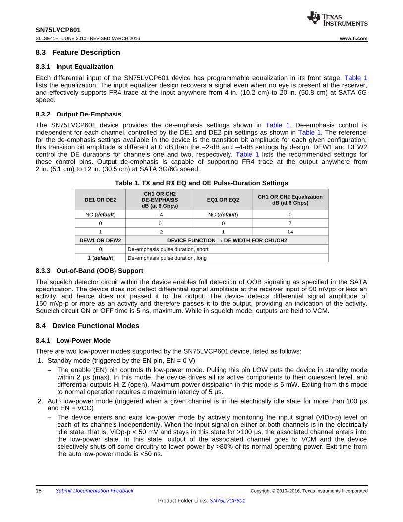
8.3.1 Input EqualizationEach differential input of the SN75LVCP601 device has programmable equalization in its front stage. Table 1lists the equalization. The input equalizer design recovers a signal even when no eye is present at the receiver,and effectively supports FR4 trace at the input anywhere from 4 in. (10.2 cm) to 20 in. (50.8 cm) at SATA 6Gspeed.
8.3.2 Output De-EmphasisThe SN75LVCP601 device provides the de-emphasis settings shown in Table 1. De-emphasis control isindependent for each channel, controlled by the DE1 and DE2 pin settings as shown in Table 1. The referencefor the de-emphasis settings available in the device is the transition bit amplitude for each given configuration;this transition bit amplitude is different at 0 dB than the –2-dB and –4-dB settings by design. DEW1 and DEW2control the DE durations for channels one and two, respectively. Table 1 lists the recommended settings forthese control pins. Output de-emphasis is capable of supporting FR4 trace at the output anywhere from2 in. (5.1 cm) to 12 in. (30.5 cm) at SATA 3G/6G speed.
Table 1. TX and RX EQ and DE Pulse-Duration Settings
DE1 OR DE2CH1 OR CH2
DE-EMPHASISdB (at 6 Gbps)
EQ1 OR EQ2 CH1 OR CH2 EqualizationdB (at 6 Gbps)
NC (default) –4 NC (default) 00 0 0 71 –2 1 14
DEW1 OR DEW2 DEVICE FUNCTION → DE WIDTH FOR CH1/CH20 De-emphasis pulse duration, short
1 (default) De-emphasis pulse duration, long
8.3.3 Out-of-Band (OOB) SupportThe squelch detector circuit within the device enables full detection of OOB signaling as specified in the SATAspecification. The device does not detect differential signal amplitude at the receiver input of 50 mVpp or less anactivity, and hence does not passed it to the output. The device detects differential signal amplitude of150 mVp-p or more as an activity and therefore passes it to the output, providing an indication of the activity.Squelch circuit ON or OFF time is 5 ns, maximum. While in squelch mode, outputs are held to VCM.
8.4 Device Functional Modes
8.4.1 Low-Power ModeThere are two low-power modes supported by the SN75LVCP601 device, listed as follows:1. Standby mode (triggered by the EN pin, EN = 0 V)
– The enable (EN) pin controls th low-power mode. Pulling this pin LOW puts the device in standby modewithin 2 µs (max). In this mode, the device drives all its active components to their quiescent level, anddifferential outputs Hi-Z (open). Maximum power dissipation in this mode is 5 mW. Exiting from this modeto normal operation requires a maximum latency of 5 µs.
2. Auto low-power mode (triggered when a given channel is in the electrically idle state for more than 100 µsand EN = VCC)– The device enters and exits low-power mode by actively monitoring the input signal (VIDp-p) level on
each of its channels independently. When the input signal on either or both channels is in the electricallyidle state, that is, VIDp-p < 50 mV and stays in this state for >100 µs, the associated channel enters intothe low-power state. In this state, output of the associated channel goes to VCM and the deviceselectively shuts off some circuitry to lower power by >80% of its normal operating power. Exit time fromthe auto low-power mode is <50 ns.

R = SN75LVCP601
ICH
R
Notebook Dock
Dock
Co
nnecto
r
Notebook Dock
HDD
eSATA Cable
(2m)
eSATA
connector
19
SN75LVCP601www.ti.com SLLSE41H –JUNE 2010–REVISED MARCH 2016
Product Folder Links: SN75LVCP601
Submit Documentation FeedbackCopyright © 2010–2016, Texas Instruments Incorporated
9 Application and Implementation
NOTEInformation in the following applications sections is not part of the TI componentspecification, and TI does not warrant its accuracy or completeness. TI’s customers areresponsible for determining suitability of components for their purposes. Customers shouldvalidate and test their design implementation to confirm system functionality.
9.1 Application InformationThe SN75LVCP601 is a dual-channel SATA redriver and signal conditioner supporting data rates of 6 Gbps. Theinputs incorporate an OOB (out-of-band) detector, which automatically squelches the output while maintaining astable common-mode voltage compliant to the SATA link.
Figure 26. Typical SN75LVCP601 Placement in the System
9.2 Typical ApplicationThis typical application describes how to configure the EQ, DE, and DEW configuration pins of theSN75LVCP601 device based on board trace length between the SATA Host and the SN75LVCP601 and theSN75LVCP601 and SATA Device. Actual configuration settings may differ due to additional factors such asboard layout, trace widths, and connectors used in the signal path.

15
14
13
12
11
1
2
3
4
5
3.3 V
LVCP601 RTJ
RX1P
RX1N
TX2N
TX2P
TX1P
TX1N
RX2N
RX2P
10 nF
10 nF
10 nF
10 nF
10 nF
10 nF
10 nF
10 nF
EQ
2
EQ
1
DE
W1
20
19
18
17
16
6 7 8 9 10
1.0
Fm
1.0
Fm
1.0
Fm
SA
TA
Ho
st
SA
TA
Co
nn
ecto
r
DE
W2
EN
DE
2
DE
1
Vcc
Vcc
Copyright © 2016, Texas Instruments Incorporated
20
SN75LVCP601SLLSE41H –JUNE 2010–REVISED MARCH 2016 www.ti.com
Product Folder Links: SN75LVCP601
Submit Documentation Feedback Copyright © 2010–2016, Texas Instruments Incorporated
Typical Application (continued)
(1) Place supply capacitors close to device pin.(2) With no external control is implemented, one can leave EN open or tie it to the supply .(3) Output de-emphasis setting is for –2 dB, EQ for 7 dB, and DE duration for SATA I/II/III operation for both channels.(4) Actual EQ/DE duration settings depend on device placement relative to host and SATA connector.
Figure 27. Typical Device Implementation
9.2.1 Design RequirementsTypically, system trace length from the SATA host to the SN75LVCP601 device and trace length from theSN75LVCP601 device to a SATA device differ and require different equalization and de-emphasis settings forthe host side and device side.
For example:• A system with a 6-inch trace from the SN75LVCP601 device to a SATA host may set EQ1 (Rx1±) to 7 dB,
and DE2 (Tx2±) to –2 dB and DEW2 (Tx2±) to long pulse duration.• The same system with a 1-inch trace from the SN75LVCP601 device to a SATA HDD may set EQ2 (Rx2±) to
0 dB, and DE1 (Tx1±) to 0 dB and DEW1 (Tx1±) to short pulse duration.
Refer to Application Curves for recommended EQ, DE and DEW settings based on trace length. It is highlyrecommended to add both pullup- and pulldown-resistor options in the layout to fine-tune the settings if needed.
Input Signal Characteristics:• Data Rate: 6 Gbps• Pattern: PRBS7• No pre-emphasis• Signal amplitude: 500 mVp-p• 18-inch SMA cable from test equipment to input and output trace

Lecroy PERT3 SN75LVCP601 25-GHz Scope
Input Output
TP1 TP2 TP3 TP4
21
SN75LVCP601www.ti.com SLLSE41H –JUNE 2010–REVISED MARCH 2016
Product Folder Links: SN75LVCP601
Submit Documentation FeedbackCopyright © 2010–2016, Texas Instruments Incorporated
Typical Application (continued)
Figure 28. Measurement Set-up
9.2.2 Detailed Design Procedure
9.2.2.1 Equalization ConfigurationEach differential input of the SN75LVCP601 device has programmable equalization in the front stage. Theequalization setting is shown in Table 2. The input equalizer is designed to recover a signal even when no eye ispresent at the receiver and effectively supports FR4 trace input from 3 inches to greater than 24 inches atSATA 6 Gbps speed.
Table 2. Equalization SettingsEQ1, EQ2 CH1, CH2 EQUALIZATION dB (AT 6 Gbps)
NC 00 71 14
9.2.2.2 De-emphasis ConfigurationThe SN75LVCP601 device provides the de-emphasis settings shown in Table 3. De-emphasis is controlledindependently for each channel and is set by the DE1, DE2, DEW1 and DEW2 pins of the SN75LVCP601device. The recommended settings for these pins are listed in Application Curves. Output de-emphasis iscapable of supporting FR4 trace lengths at the output from 3 inches to 12+ inches at SATA 6 Gbps speed.
Table 3. De-emphasis SettingsDE1, DE2 CH1, CH2 DE-EMPHASIS dB (AT 6 Gbps)
0 01 –2
NC –4
Table 4. DE Width ControlDEW1, DEW2 DE-EMPHASIS WIDTH FOR CH1, CH2
0 Short de-emphasis pulse duration1 Long de-emphasis pulse duration
22
SN75LVCP601SLLSE41H –JUNE 2010–REVISED MARCH 2016 www.ti.com
Product Folder Links: SN75LVCP601
Submit Documentation Feedback Copyright © 2010–2016, Texas Instruments Incorporated
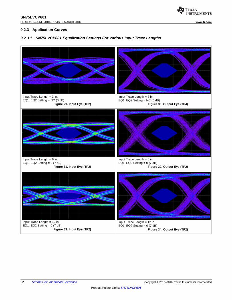
9.2.3 Application Curves
9.2.3.1 SN75LVCP601 Equalization Settings For Various Input Trace Lengths
Input Trace Length = 3 in.EQ1, EQ2 Setting = NC (0 dB)
Figure 29. Input Eye (TP2)
Input Trace Length = 3 in.EQ1, EQ2 Setting = NC (0 dB)
Figure 30. Output Eye (TP4)
Input Trace Length = 6 in.EQ1, EQ2 Setting = 0 (7 dB)
Figure 31. Input Eye (TP2)
Input Trace Length = 6 in.EQ1, EQ2 Setting = 0 (7 dB)
Figure 32. Output Eye (TP2)
Input Trace Length = 12 in.EQ1, EQ2 Setting = 0 (7 dB)
Figure 33. Input Eye (TP2)
Input Trace Length = 12 in.EQ1, EQ2 Setting = 0 (7 dB)
Figure 34. Output Eye (TP2)

23
SN75LVCP601www.ti.com SLLSE41H –JUNE 2010–REVISED MARCH 2016
Product Folder Links: SN75LVCP601
Submit Documentation FeedbackCopyright © 2010–2016, Texas Instruments Incorporated
Input Trace Length = 24 in.EQ1, EQ2 Setting = 0 (7 dB)
Figure 35. Input Eye (TP2)
Input Trace Length = 24 in.EQ1, EQ2 Setting = 0 (7 dB)
Figure 36. Output Eye (TP2)
Input Trace Length = 36 in.EQ1, EQ2 Setting = 1 (14 dB)
Figure 37. Input Eye (TP2)
Input Trace Length = 36 in.EQ1, EQ2 Setting = 1 (14 dB)
Figure 38. Output Eye (TP2)
Input Trace Length = 48 in.EQ1, EQ2 Setting = 1 (14 dB)
Figure 39. Input Eye (TP2)
Input Trace Length = 36 in.EQ1, EQ2 Setting = 1 (14 dB)
Figure 40. Output Eye (TP2)

24
SN75LVCP601SLLSE41H –JUNE 2010–REVISED MARCH 2016 www.ti.com
Product Folder Links: SN75LVCP601
Submit Documentation Feedback Copyright © 2010–2016, Texas Instruments Incorporated
9.2.3.2 SN75LVCP601 De-emphasis Settings For Various Output Trace Lengths
Output Trace Length = 0 in.DE1, DE2 Setting = 0 (0 dB)DEW1, DEW2 Setting = 0 (Short pulse duration)
Figure 41. Output Eye (TP4)
Output Trace Length = 3 in.DE1, DE2 Setting = 0 (0 dB)DEW1, DEW2 Setting = 0 (Short pulse duration)
Figure 42. Output Eye (TP4)
Output Trace Length = 6 in.DE1, DE2 Setting = 1 (–2 dB)DEW1, DEW2 Setting = 1 (Long pulse duration)
Figure 43. Output Eye (TP4)
Output Trace Length = 12 in.DE1, DE2 Setting = 1 (–2 dB)DEW1, DEW2 Setting = 1 (Long pulse duration)
Figure 44. Output Eye (TP4)
Output Trace Length = 12 in.DE1, DE2 Setting = NC (–4 dBDEW1, DEW2 Setting = 1 (Long pulse duration)
Figure 45. Output Eye (TP4)

16 in. (40.6 cm)
24 in. (61 cm)
SATA Host Redriver
Redriver on Motherboard
Main Board
SATA HostRedriver
Dock Board
Redriver on Dock Board
SATAConnector
SATAConnector
16 in. (40.6 cm) 8 in.(20.3 cm)
8 in.(20.3 cm)
24 in. (61 cm)
25
SN75LVCP601www.ti.com SLLSE41H –JUNE 2010–REVISED MARCH 2016
Product Folder Links: SN75LVCP601
Submit Documentation FeedbackCopyright © 2010–2016, Texas Instruments Incorporated
10 Power Supply RecommendationsThe design of SN75LVCP601 device is for operation from one 3.3-V supply. Always practice proper power-supply sequencing procedure. Apply VCC first, before application of any input signals to the device. The power-down sequence is in reverse order.
11 Layout
11.1 Layout Guidelines
Example: Suggested trace-length values are values based on TI spice simulations (done over programmable limits ofinput EQ and output de-emphasis) to meet SATA loss and jitter specification.Actual trace length supported by the LVCP601 may be more or less than suggested values and depends on boardlayout, trace widths, and number of connectors used in the SATA signal path.
Figure 46. Trace Length Example for LVCP601

HIGH SPEED TRACES
LENGTH MATCHING
26
SN75LVCP601SLLSE41H –JUNE 2010–REVISED MARCH 2016 www.ti.com
Product Folder Links: SN75LVCP601
Submit Documentation Feedback Copyright © 2010–2016, Texas Instruments Incorporated
11.2 Layout Example
Figure 47. SN65LVCP601 EVM

27
SN75LVCP601www.ti.com SLLSE41H –JUNE 2010–REVISED MARCH 2016
Product Folder Links: SN75LVCP601
Submit Documentation FeedbackCopyright © 2010–2016, Texas Instruments Incorporated
12 Device and Documentation Support
12.1 Community ResourcesThe following links connect to TI community resources. Linked contents are provided "AS IS" by the respectivecontributors. They do not constitute TI specifications and do not necessarily reflect TI's views; see TI's Terms ofUse.
TI E2E™ Online Community TI's Engineer-to-Engineer (E2E) Community. Created to foster collaborationamong engineers. At e2e.ti.com, you can ask questions, share knowledge, explore ideas and helpsolve problems with fellow engineers.
Design Support TI's Design Support Quickly find helpful E2E forums along with design support tools andcontact information for technical support.
12.2 TrademarksE2E is a trademark of Texas Instruments.All other trademarks are the property of their respective owners.
12.3 Electrostatic Discharge CautionThese devices have limited built-in ESD protection. The leads should be shorted together or the device placed in conductive foamduring storage or handling to prevent electrostatic damage to the MOS gates.
12.4 GlossarySLYZ022 — TI Glossary.
This glossary lists and explains terms, acronyms, and definitions.
13 Mechanical, Packaging, and Orderable InformationThe following pages include mechanical, packaging, and orderable information. This information is the mostcurrent data available for the designated devices. This data is subject to change without notice and revision ofthis document. For browser-based versions of this data sheet, refer to the left-hand navigation.

PACKAGE OPTION ADDENDUM
www.ti.com 10-Dec-2020
Addendum-Page 1
PACKAGING INFORMATION
Orderable Device Status(1)
Package Type PackageDrawing
Pins PackageQty
Eco Plan(2)
Lead finish/Ball material
(6)
MSL Peak Temp(3)
Op Temp (°C) Device Marking(4/5)
Samples
SN75LVCP601RTJR ACTIVE QFN RTJ 20 3000 RoHS & Green Call TI | NIPDAU Level-2-260C-1 YEAR 0 to 85 LVC601
SN75LVCP601RTJT ACTIVE QFN RTJ 20 250 RoHS & Green Call TI | NIPDAU Level-2-260C-1 YEAR 0 to 85 LVC601
(1) The marketing status values are defined as follows:ACTIVE: Product device recommended for new designs.LIFEBUY: TI has announced that the device will be discontinued, and a lifetime-buy period is in effect.NRND: Not recommended for new designs. Device is in production to support existing customers, but TI does not recommend using this part in a new design.PREVIEW: Device has been announced but is not in production. Samples may or may not be available.OBSOLETE: TI has discontinued the production of the device.
(2) RoHS: TI defines "RoHS" to mean semiconductor products that are compliant with the current EU RoHS requirements for all 10 RoHS substances, including the requirement that RoHS substancedo not exceed 0.1% by weight in homogeneous materials. Where designed to be soldered at high temperatures, "RoHS" products are suitable for use in specified lead-free processes. TI mayreference these types of products as "Pb-Free".RoHS Exempt: TI defines "RoHS Exempt" to mean products that contain lead but are compliant with EU RoHS pursuant to a specific EU RoHS exemption.Green: TI defines "Green" to mean the content of Chlorine (Cl) and Bromine (Br) based flame retardants meet JS709B low halogen requirements of <=1000ppm threshold. Antimony trioxide basedflame retardants must also meet the <=1000ppm threshold requirement.
(3) MSL, Peak Temp. - The Moisture Sensitivity Level rating according to the JEDEC industry standard classifications, and peak solder temperature.
(4) There may be additional marking, which relates to the logo, the lot trace code information, or the environmental category on the device.
(5) Multiple Device Markings will be inside parentheses. Only one Device Marking contained in parentheses and separated by a "~" will appear on a device. If a line is indented then it is a continuationof the previous line and the two combined represent the entire Device Marking for that device.
(6) Lead finish/Ball material - Orderable Devices may have multiple material finish options. Finish options are separated by a vertical ruled line. Lead finish/Ball material values may wrap to twolines if the finish value exceeds the maximum column width.
Important Information and Disclaimer:The information provided on this page represents TI's knowledge and belief as of the date that it is provided. TI bases its knowledge and belief on informationprovided by third parties, and makes no representation or warranty as to the accuracy of such information. Efforts are underway to better integrate information from third parties. TI has taken andcontinues to take reasonable steps to provide representative and accurate information but may not have conducted destructive testing or chemical analysis on incoming materials and chemicals.TI and TI suppliers consider certain information to be proprietary, and thus CAS numbers and other limited information may not be available for release.
In no event shall TI's liability arising out of such information exceed the total purchase price of the TI part(s) at issue in this document sold by TI to Customer on an annual basis.

PACKAGE OPTION ADDENDUM
www.ti.com 10-Dec-2020
Addendum-Page 2

TAPE AND REEL INFORMATION
*All dimensions are nominal
Device PackageType
PackageDrawing
Pins SPQ ReelDiameter
(mm)
ReelWidth
W1 (mm)
A0(mm)
B0(mm)
K0(mm)
P1(mm)
W(mm)
Pin1Quadrant
SN75LVCP601RTJR QFN RTJ 20 3000 330.0 12.4 4.25 4.25 1.15 8.0 12.0 Q2
SN75LVCP601RTJT QFN RTJ 20 250 180.0 12.4 4.25 4.25 1.15 8.0 12.0 Q2
PACKAGE MATERIALS INFORMATION
www.ti.com 29-Sep-2019
Pack Materials-Page 1

*All dimensions are nominal
Device Package Type Package Drawing Pins SPQ Length (mm) Width (mm) Height (mm)
SN75LVCP601RTJR QFN RTJ 20 3000 367.0 367.0 35.0
SN75LVCP601RTJT QFN RTJ 20 250 210.0 185.0 35.0
PACKAGE MATERIALS INFORMATION
www.ti.com 29-Sep-2019
Pack Materials-Page 2

www.ti.com
GENERIC PACKAGE VIEW
This image is a representation of the package family, actual package may vary.Refer to the product data sheet for package details.
WQFN - 0.8 mm max heightRTJ 20PLASTIC QUAD FLATPACK - NO LEAD4 x 4, 0.5 mm pitch
4224842/A


IMPORTANT NOTICE AND DISCLAIMERTI PROVIDES TECHNICAL AND RELIABILITY DATA (INCLUDING DATASHEETS), DESIGN RESOURCES (INCLUDING REFERENCEDESIGNS), APPLICATION OR OTHER DESIGN ADVICE, WEB TOOLS, SAFETY INFORMATION, AND OTHER RESOURCES “AS IS”AND WITH ALL FAULTS, AND DISCLAIMS ALL WARRANTIES, EXPRESS AND IMPLIED, INCLUDING WITHOUT LIMITATION ANYIMPLIED WARRANTIES OF MERCHANTABILITY, FITNESS FOR A PARTICULAR PURPOSE OR NON-INFRINGEMENT OF THIRDPARTY INTELLECTUAL PROPERTY RIGHTS.These resources are intended for skilled developers designing with TI products. You are solely responsible for (1) selecting the appropriateTI products for your application, (2) designing, validating and testing your application, and (3) ensuring your application meets applicablestandards, and any other safety, security, or other requirements. These resources are subject to change without notice. TI grants youpermission to use these resources only for development of an application that uses the TI products described in the resource. Otherreproduction and display of these resources is prohibited. No license is granted to any other TI intellectual property right or to any third partyintellectual property right. TI disclaims responsibility for, and you will fully indemnify TI and its representatives against, any claims, damages,costs, losses, and liabilities arising out of your use of these resources.TI’s products are provided subject to TI’s Terms of Sale (https:www.ti.com/legal/termsofsale.html) or other applicable terms available eitheron ti.com or provided in conjunction with such TI products. TI’s provision of these resources does not expand or otherwise alter TI’sapplicable warranties or warranty disclaimers for TI products.IMPORTANT NOTICE
Mailing Address: Texas Instruments, Post Office Box 655303, Dallas, Texas 75265Copyright © 2021, Texas Instruments Incorporated