PSMN017-30PL N-channel 30 V 17 mΩ logic level …. Product profile 1.1 General description Logic...
14
1. Product profile 1.1 General description Logic level N-channel MOSFET in TO220 package qualified to 175 °C. This product is designed and qualified for use in a wide range of industrial, communications and domestic equipment. 1.2 Features and benefits High efficiency due to low switching and conduction losses Suitable for logic level gate drive sources 1.3 Applications DC-to-DC converters Load switching Motor control Server power supplies 1.4 Quick reference data [1] Continuous current is limited by package. PSMN017-30PL N-channel 30 V 17 mΩ logic level MOSFET in TO220 Rev. 2 — 3 April 2012 Product data sheet Table 1. Quick reference data Symbol Parameter Conditions Min Typ Max Unit V DS drain-source voltage T j ≥ 25 °C; T j ≤ 175 °C - - 30 V I D drain current T mb = 25 °C; V GS = 10 V; see Figure 1 [1] - - 32 A P tot total power dissipation T mb = 25 °C; see Figure 2 - - 45 W T j junction temperature -55 - 175 °C Static characteristics R DSon drain-source on-state resistance V GS = 4.5 V; I D = 10 A; T j = 25 °C; see Figure 13 - 18.7 23.4 mΩ V GS = 10 V; I D = 10 A; T j = 25 °C; see Figure 13 - 13.4 17 mΩ Dynamic characteristics Q GD gate-drain charge V GS = 4.5 V; I D = 10 A; V DS = 15 V; see Figure 14 ; see Figure 15 - 1.94 - nC Q G(tot) total gate charge V GS = 4.5 V; I D = 10 A; V DS = 15 V; see Figure 14 ; see Figure 15 - 5.1 - nC Avalanche ruggedness E DS(AL)S non-repetitive drain-source avalanche energy V GS = 10 V; T j(init) = 25 °C; I D = 32 A; V sup ≤ 30 V; R GS = 50 Ω; unclamped - - 13 mJ
-
Upload
trinhduong -
Category
Documents
-
view
216 -
download
2
Transcript of PSMN017-30PL N-channel 30 V 17 mΩ logic level …. Product profile 1.1 General description Logic...
1. Product profile
1.1 General description
Logic level N-channel MOSFET in TO220 package qualified to 175 °C. This product is designed and qualified for use in a wide range of industrial, communications and domestic equipment.
1.2 Features and benefits
High efficiency due to low switching and conduction losses
Suitable for logic level gate drive sources
1.3 Applications
DC-to-DC converters
Load switching
Motor control
Server power supplies
1.4 Quick reference data
[1] Continuous current is limited by package.
PSMN017-30PLN-channel 30 V 17 mΩ logic level MOSFET in TO220Rev. 2 — 3 April 2012 Product data sheet
Table 1. Quick reference data
Symbol Parameter Conditions Min Typ Max Unit
VDS drain-source voltage Tj ≥ 25 °C; Tj ≤ 175 °C - - 30 V
ID drain current Tmb = 25 °C; VGS = 10 V; see Figure 1 [1] - - 32 A
Ptot total power dissipation Tmb = 25 °C; see Figure 2 - - 45 W
Tj junction temperature -55 - 175 °C
Static characteristics
RDSon drain-source on-state resistance
VGS = 4.5 V; ID = 10 A; Tj = 25 °C; see Figure 13
- 18.7 23.4 mΩ
VGS = 10 V; ID = 10 A; Tj = 25 °C; see Figure 13
- 13.4 17 mΩ
Dynamic characteristics
QGD gate-drain charge VGS = 4.5 V; ID = 10 A; VDS = 15 V; see Figure 14; see Figure 15
- 1.94 - nC
QG(tot) total gate charge VGS = 4.5 V; ID = 10 A; VDS = 15 V; see Figure 14; see Figure 15
- 5.1 - nC
Avalanche ruggedness
EDS(AL)S non-repetitive drain-source avalanche energy
VGS = 10 V; Tj(init) = 25 °C; ID = 32 A; Vsup ≤ 30 V; RGS = 50 Ω; unclamped
- - 13 mJ
Nexperia PSMN017-30PLN-channel 30 V 17 mΩ logic level MOSFET in TO220
2. Pinning information
3. Ordering information
4. Limiting values
[1] Continuous current is limited by package.
Table 2. Pinning information
Pin Symbol Description Simplified outline Graphic symbol
1 G gate
SOT78 (TO-220AB)
2 D drain
3 S source
mb D mounting base; connected to drain
1 2
mb
3
S
D
G
mbb076
Table 3. Ordering information
Type number Package
Name Description Version
PSMN017-30PL TO-220AB plastic single-ended package; heatsink mounted; 1 mounting hole; 3-lead TO-220AB
SOT78
Table 4. Limiting valuesIn accordance with the Absolute Maximum Rating System (IEC 60134).
Symbol Parameter Conditions Min Max Unit
VDS drain-source voltage Tj ≥ 25 °C; Tj ≤ 175 °C - 30 V
VDGR drain-gate voltage Tj ≥ 25 °C; Tj ≤ 175 °C; RGS = 20 kΩ - 30 V
VGS gate-source voltage -20 20 V
ID drain current VGS = 10 V; Tmb = 100 °C; see Figure 1 [1] - 26.9 A
VGS = 10 V; Tmb = 25 °C; see Figure 1 [1] - 32 A
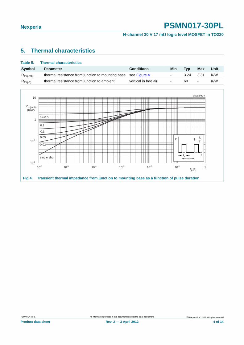
IDM peak drain current pulsed; tp ≤ 10 µs; Tmb = 25 °C; see Figure 3 - 152 A
Ptot total power dissipation Tmb = 25 °C; see Figure 2 - 45 W
Tstg storage temperature -55 175 °C
Tj junction temperature -55 175 °C
Source-drain diode
IS source current Tmb = 25 °C - 32 A
ISM peak source current pulsed; tp ≤ 10 µs; Tmb = 25 °C - 152 A
Avalanche ruggedness
EDS(AL)S non-repetitive drain-source avalanche energy
VGS = 10 V; Tj(init) = 25 °C; ID = 32 A; Vsup ≤ 30 V; RGS = 50 Ω; unclamped
- 13 mJ
© Nexperia B.V. 2017. All rights reservedPSMN017-30PL All information provided in this document is subject to legal disclaimers.
Product data sheet Rev. 2 — 3 April 2012 2 of 14
Nexperia PSMN017-30PLN-channel 30 V 17 mΩ logic level MOSFET in TO220
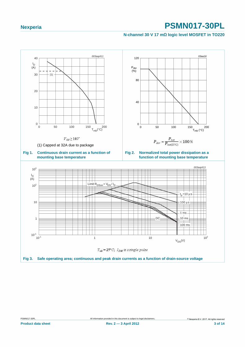
(1) Capped at 32A due to package
Fig 1. Continuous drain current as a function of mounting base temperature
Fig 2. Normalized total power dissipation as a function of mounting base temperature
Fig 3. Safe operating area; continuous and peak drain currents as a function of drain-source voltage
003aaj411
0
10
20
30
40
0 50 100 150 200Tmb (°C)
ID (A)
(1)
Tmb (°C)0 20015050 100
03aa16
40
80
120
Pder(%)
0
003aaj413
10-1
1
10
102
103
10-1 1 10 102
VDS (V)
ID(A)
Limit RDSon = V DS / ID
DC
100 μs
10 ms
tp =10 μs
100 ms
1 ms
© Nexperia B.V. 2017. All rights reservedPSMN017-30PL All information provided in this document is subject to legal disclaimers.
Product data sheet Rev. 2 — 3 April 2012 3 of 14
Nexperia PSMN017-30PLN-channel 30 V 17 mΩ logic level MOSFET in TO220
5. Thermal characteristics
Table 5. Thermal characteristics
Symbol Parameter Conditions Min Typ Max Unit
Rth(j-mb) thermal resistance from junction to mounting base see Figure 4 - 3.24 3.31 K/W
Rth(j-a) thermal resistance from junction to ambient vertical in free air - 60 - K/W
Fig 4. Transient thermal impedance from junction to mounting base as a function of pulse duration
003aaj414
single shot
0.2
0.1
0.05
10-2
10-1
1
10
10-5 10-4 10-3 10-2 10-1 1tp (s)
Zth(j-mb) (K/W)
δ = 0.5
0.02
tpT
P
t
tpT
δ =
10-6
© Nexperia B.V. 2017. All rights reservedPSMN017-30PL All information provided in this document is subject to legal disclaimers.
Product data sheet Rev. 2 — 3 April 2012 4 of 14
Nexperia PSMN017-30PLN-channel 30 V 17 mΩ logic level MOSFET in TO220
6. Characteristics
Table 6. Characteristics
Symbol Parameter Conditions Min Typ Max Unit
Static characteristics
V(BR)DSS drain-source breakdown voltage ID = 250 µA; VGS = 0 V; Tj = 25 °C 30 - - V
ID = 250 µA; VGS = 0 V; Tj = -55 °C 27 - - V
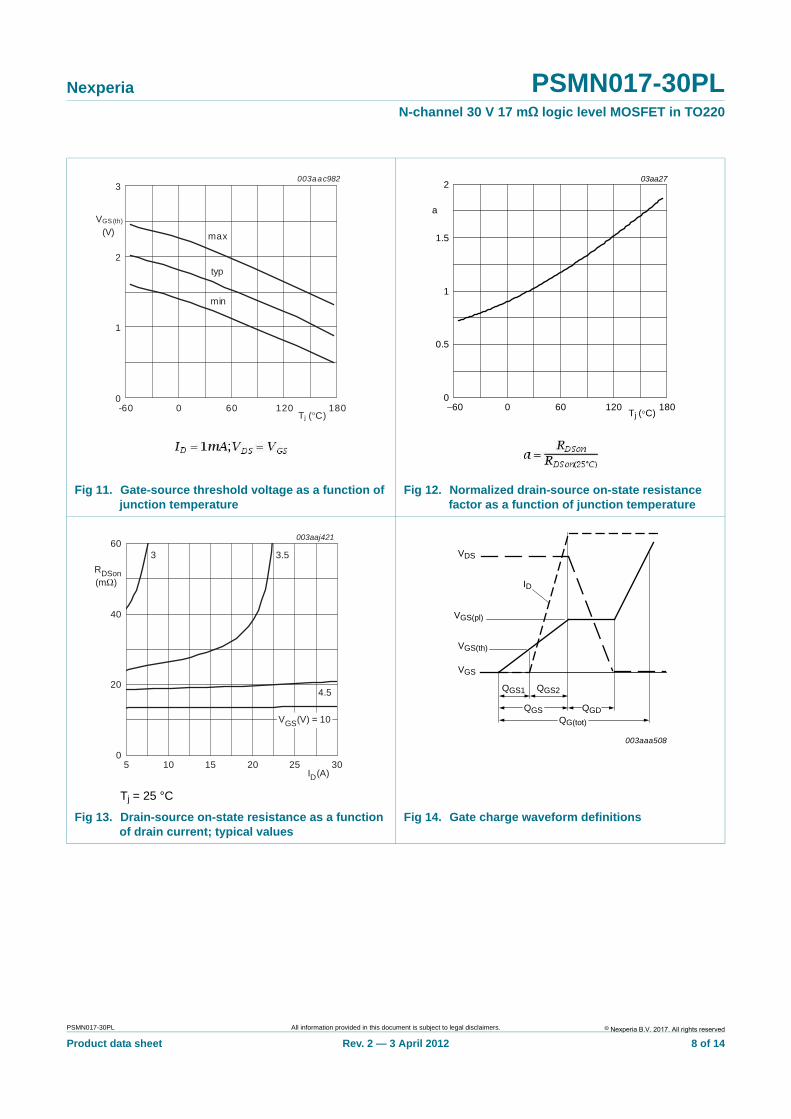
VGS(th) gate-source threshold voltage ID = 1 mA; VDS = VGS; Tj = 25 °C; see Figure 10; see Figure 11
1.3 1.7 2.15 V
ID = 1 mA; VDS = VGS; Tj = 175 °C; see Figure 11
0.5 - - V
ID = 1 mA; VDS = VGS; Tj = -55 °C; see Figure 11
- - 2.45 V
IDSS drain leakage current VDS = 30 V; VGS = 0 V; Tj = 25 °C - 0.3 1 µA
VDS = 30 V; VGS = 0 V; Tj = 125 °C - - 50 µA
IGSS gate leakage current VGS = 16 V; VDS = 0 V; Tj = 25 °C - 10 100 nA
VGS = -16 V; VDS = 0 V; Tj = 25 °C - 10 100 nA
RDSon drain-source on-state resistance
VGS = 4.5 V; ID = 10 A; Tj = 175 °C; see Figure 12
- - 43.2 mΩ
VGS = 4.5 V; ID = 10 A; Tj = 25 °C; see Figure 13
- 18.7 23.4 mΩ
VGS = 10 V; ID = 10 A; Tj = 175 °C; see Figure 12
- 24 31.5 mΩ
VGS = 10 V; ID = 10 A; Tj = 100 °C; see Figure 12
- - 23.5 mΩ
VGS = 10 V; ID = 10 A; Tj = 25 °C; see Figure 13
- 13.4 17 mΩ
RG gate resistance f = 1 MHz - 2.03 - Ω
Dynamic characteristics
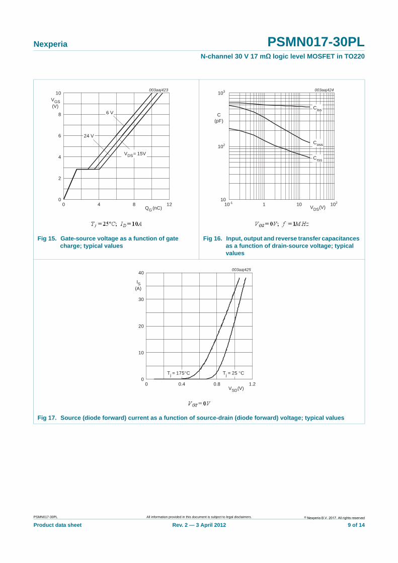
QG(tot) total gate charge ID = 10 A; VDS = 15 V; VGS = 10 V; see Figure 14; see Figure 15
- 10.7 - nC
ID = 0 A; VDS = 0 V; VGS = 10 V; see Figure 14; see Figure 15
- 9.55 - nC
ID = 10 A; VDS = 15 V; VGS = 4.5 V; see Figure 14; see Figure 15
- 5.1 - nC
QGS gate-source charge ID = 10 A; VDS = 15 V; VGS = 4.5 V; see Figure 14; see Figure 15
- 1.52 - nC
QGS(th) pre-threshold gate-source charge
- 1 - nC
QGS(th-pl) post-threshold gate-source charge
- 0.5 - nC
QGD gate-drain charge - 1.94 - nC
VGS(pl) gate-source plateau voltage ID = 10 A; VDS = 15 V; see Figure 14; see Figure 15
- 2.86 - V
Ciss input capacitance VDS = 15 V; VGS = 0 V; f = 1 MHz; Tj = 25 °C; see Figure 16
- 552 - pF
Coss output capacitance - 127 - pF
Crss reverse transfer capacitance - 64 - pF
© Nexperia B.V. 2017. All rights reservedPSMN017-30PL All information provided in this document is subject to legal disclaimers.
Product data sheet Rev. 2 — 3 April 2012 5 of 14
Nexperia PSMN017-30PLN-channel 30 V 17 mΩ logic level MOSFET in TO220
td(on) turn-on delay time VDS = 15 V; RL = 1.5 Ω; VGS = 4.5 V; RG(ext) = 5 Ω
- 10.7 - ns
tr rise time - 9.2 - ns
td(off) turn-off delay time - 11.4 - ns
tf fall time - 5.1 - ns
Source-drain diode
VSD source-drain voltage IS = 10 A; VGS = 0 V; Tj = 25 °C; see Figure 17
- 0.89 1.2 V
trr reverse recovery time IS = 10 A; dIS/dt = -100 A/µs; VGS = 0 V; VDS = 15 V
- 17.3 - ns
Qr recovered charge - 6.5 - nC
Table 6. Characteristics …continued
Symbol Parameter Conditions Min Typ Max Unit
Tj = 25 °C
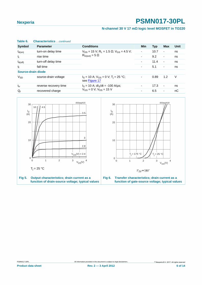
Fig 5. Output characteristics; drain current as a function of drain-source voltage; typical values
Fig 6. Transfer characteristics; drain current as a function of gate-source voltage; typical values
003aaj415
0
10
20
30
0 1 2 3 4VDS (V)
ID(A)
VGS (V) = 2.4
2.8
3.5
4.5 10
3
003aaj418
0
10
20
30
0 1 2 3 4VGS (V)
ID(A)
Tj = 25 °CTj = 175 °C
© Nexperia B.V. 2017. All rights reservedPSMN017-30PL All information provided in this document is subject to legal disclaimers.
Product data sheet Rev. 2 — 3 April 2012 6 of 14

Nexperia PSMN017-30PLN-channel 30 V 17 mΩ logic level MOSFET in TO220
Fig 7. Input and reverse transfer capacitances as a function of gate-source voltage; typical values
Fig 8. Forward transconductance as a function of drain current; typical values
Fig 9. Drain-source on-state resistance as a function of gate-source voltage; typical values
Fig 10. Sub-threshold drain current as a function of gate-source voltage
003aaj532
0
200
400
600
800
1000
0 3 6 9 12VGS (V)
C (pF)
Ciss
Crss
003aaj417
0
10
20
30
0 10 20 30ID (A)
gfs(S)
003aaj416
10
20
30
40
0 4 8 12 16VGS (V)
RDSon(mΩ)
003aab271
10-6
10-5
10-4
10-3
10-2
10-1
0 1 2 3VGS (V)
ID
(A)
maxtypmin
© Nexperia B.V. 2017. All rights reservedPSMN017-30PL All information provided in this document is subject to legal disclaimers.
Product data sheet Rev. 2 — 3 April 2012 7 of 14
Nexperia PSMN017-30PLN-channel 30 V 17 mΩ logic level MOSFET in TO220
Fig 11. Gate-source threshold voltage as a function of junction temperature
Fig 12. Normalized drain-source on-state resistance factor as a function of junction temperature
Tj = 25 °C
Fig 13. Drain-source on-state resistance as a function of drain current; typical values
Fig 14. Gate charge waveform definitions
003aac982
0
1
2
3
-60 0 60 120 180Tj (°C)
VGS(th)
(V) max
typ
min
03aa27
0
0.5
1
1.5
2
−60 0 60 120 180Tj (°C)
a
003aaj421
0
20
40
60
5 10 15 20 25 30ID (A)
RDSon(mΩ)
4.5
VGS (V) = 10
3 3.5
003aaa508
VGS
VGS(th)
QGS1 QGS2
QGD
VDS
QG(tot)
ID
QGS
VGS(pl)
© Nexperia B.V. 2017. All rights reservedPSMN017-30PL All information provided in this document is subject to legal disclaimers.
Product data sheet Rev. 2 — 3 April 2012 8 of 14
Nexperia PSMN017-30PLN-channel 30 V 17 mΩ logic level MOSFET in TO220
Fig 15. Gate-source voltage as a function of gate charge; typical values
Fig 16. Input, output and reverse transfer capacitances as a function of drain-source voltage; typical values
Fig 17. Source (diode forward) current as a function of source-drain (diode forward) voltage; typical values
003aaj423
0
2
4
6
8
10
0 4 8 12QG (nC)
VGS(V)
VDS = 15V
24 V
6 V
003aaj424
10
102
103
10-1 1 10 102
VDS (V)
C (pF)
Ciss
Crss
Coss
003aaj425
0
10
20
30
40
0 0.4 0.8 1.2VSD (V)
IS(A)
Tj = 25 °CTj = 175°C
© Nexperia B.V. 2017. All rights reservedPSMN017-30PL All information provided in this document is subject to legal disclaimers.
Product data sheet Rev. 2 — 3 April 2012 9 of 14
Nexperia PSMN017-30PLN-channel 30 V 17 mΩ logic level MOSFET in TO220
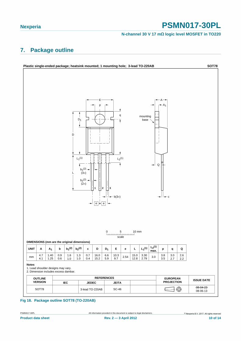
7. Package outline
Fig 18. Package outline SOT78 (TO-220AB)
REFERENCESOUTLINEVERSION
EUROPEANPROJECTION
ISSUE DATEIEC JEDEC JEITA
SOT78 SC-463-lead TO-220AB
SOT78
08-04-2308-06-13
Notes1. Lead shoulder designs may vary.2. Dimension includes excess dambar.
UNIT A
mm 4.74.1
1.401.25
0.90.6
0.70.4
16.015.2
6.65.9
10.39.7
15.012.8
3.302.79
3.83.5
A1
DIMENSIONS (mm are the original dimensions)
Plastic single-ended package; heatsink mounted; 1 mounting hole; 3-lead TO-220AB
0 5 10 mm
scale
b b1(2)
1.61.0
c D
1.31.0
b2(2) D1 E e
2.54
L L1(1) L2(1)
max.
3.0
p q
3.02.7
Q
2.62.2
D
D1
q
p
L
1 2 3
L1(1)
b1(2)
(3×)
b2(2)
(2×)
e e
b(3×)
AE
A1
c
Q
L2(1)
mountingbase
© Nexperia B.V. 2017. All rights reservedPSMN017-30PL All information provided in this document is subject to legal disclaimers.
Product data sheet Rev. 2 — 3 April 2012 10 of 14
Nexperia PSMN017-30PLN-channel 30 V 17 mΩ logic level MOSFET in TO220
8. Revision history
Table 7. Revision history
Document ID Release date Data sheet status Change notice Supersedes
PSMN017-30PL v.2 20120403 Product data sheet - PSMN017-30PL v.1
Modifications: • Status changed from objective to product.
• Various changes to content.
PSMN017-30PL v.1 20120228 Objective data sheet - -
© Nexperia B.V. 2017. All rights reservedPSMN017-30PL All information provided in this document is subject to legal disclaimers.
Product data sheet Rev. 2 — 3 April 2012 11 of 14
Nexperia PSMN017-30PLN-channel 30 V 17 mΩ logic level MOSFET in TO220
9. Legal information
9.1 Data sheet status
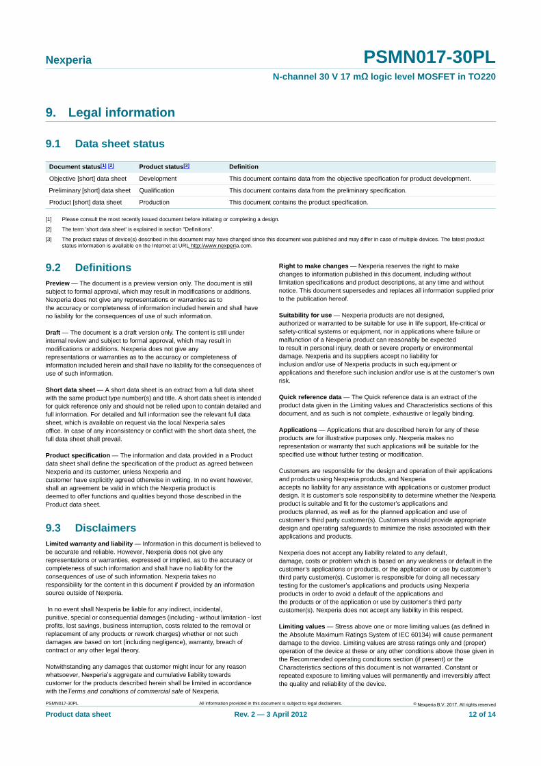
[1] Please consult the most recently issued document before initiating or completing a design.
[2] The term 'short data sheet' is explained in section "Definitions".
[3] The product status of device(s) described in this document may have changed since this document was published and may differ in case of multiple devices. The latest product status information is available on the Internet at URL http://www.nexperia.com.
9.2 DefinitionsPreview — The document is a preview version only. The document is still subject to formal approval, which may result in modifications or additions. Nexperia does not give any representations or warranties as to the accuracy or completeness of information included herein and shall have no liability for the consequences of use of such information.
Draft — The document is a draft version only. The content is still under internal review and subject to formal approval, which may result in modifications or additions. Nexperia does not give any representations or warranties as to the accuracy or completeness of information included herein and shall have no liability for the consequences of use of such information.
Short data sheet — A short data sheet is an extract from a full data sheet with the same product type number(s) and title. A short data sheet is intended for quick reference only and should not be relied upon to contain detailed and full information. For detailed and full information see the relevant full data sheet, which is available on request via the local Nexperia sales office. In case of any inconsistency or conflict with the short data sheet, the full data sheet shall prevail.
Product specification — The information and data provided in a Product data sheet shall define the specification of the product as agreed between Nexperia and its customer, unless Nexperia and customer have explicitly agreed otherwise in writing. In no event however, shall an agreement be valid in which the Nexperia product is deemed to offer functions and qualities beyond those described in the Product data sheet.
9.3 DisclaimersLimited warranty and liability — Information in this document is believed to be accurate and reliable. However, Nexperia does not give any representations or warranties, expressed or implied, as to the accuracy or completeness of such information and shall have no liability for the consequences of use of such information. Nexperia takes no responsibility for the content in this document if provided by an information source outside of Nexperia.
In no event shall Nexperia be liable for any indirect, incidental, punitive, special or consequential damages (including - without limitation - lost profits, lost savings, business interruption, costs related to the removal or replacement of any products or rework charges) whether or not such damages are based on tort (including negligence), warranty, breach of contract or any other legal theory.
Notwithstanding any damages that customer might incur for any reason whatsoever, Nexperia’s aggregate and cumulative liability towards customer for the products described herein shall be limited in accordance with theTerms and conditions of commercial sale of Nexperia.
Right to make changes — Nexperia reserves the right to make changes to information published in this document, including without limitation specifications and product descriptions, at any time and without notice. This document supersedes and replaces all information supplied prior to the publication hereof.
Suitability for use — Nexperia products are not designed, authorized or warranted to be suitable for use in life support, life-critical or safety-critical systems or equipment, nor in applications where failure or malfunction of a Nexperia product can reasonably be expected to result in personal injury, death or severe property or environmental damage. Nexperia and its suppliers accept no liability for inclusion and/or use of Nexperia products in such equipment or applications and therefore such inclusion and/or use is at the customer’s own risk.
Quick reference data — The Quick reference data is an extract of the product data given in the Limiting values and Characteristics sections of this document, and as such is not complete, exhaustive or legally binding.
Applications — Applications that are described herein for any of these products are for illustrative purposes only. Nexperia makes no representation or warranty that such applications will be suitable for the specified use without further testing or modification.
Customers are responsible for the design and operation of their applications and products using Nexperia products, and Nexperia accepts no liability for any assistance with applications or customer product design. It is customer’s sole responsibility to determine whether the Nexperia product is suitable and fit for the customer’s applications and products planned, as well as for the planned application and use of customer’s third party customer(s). Customers should provide appropriate design and operating safeguards to minimize the risks associated with their applications and products.
Nexperia does not accept any liability related to any default, damage, costs or problem which is based on any weakness or default in the customer’s applications or products, or the application or use by customer’s third party customer(s). Customer is responsible for doing all necessary testing for the customer’s applications and products using Nexperia products in order to avoid a default of the applications and the products or of the application or use by customer’s third party customer(s). Nexperia does not accept any liability in this respect.
Limiting values — Stress above one or more limiting values (as defined in the Absolute Maximum Ratings System of IEC 60134) will cause permanent damage to the device. Limiting values are stress ratings only and (proper) operation of the device at these or any other conditions above those given in the Recommended operating conditions section (if present) or the Characteristics sections of this document is not warranted. Constant or repeated exposure to limiting values will permanently and irreversibly affect the quality and reliability of the device.
Document status[1] [2] Product status[3] Definition
Objective [short] data sheet Development This document contains data from the objective specification for product development.
Preliminary [short] data sheet Qualification This document contains data from the preliminary specification.
Product [short] data sheet Production This document contains the product specification.
© Nexperia B.V. 2017. All rights reservedPSMN017-30PL All information provided in this document is subject to legal disclaimers.
Product data sheet Rev. 2 — 3 April 2012 12 of 14

Nexperia PSMN017-30PLN-channel 30 V 17 mΩ logic level MOSFET in TO220
Terms and conditions of commercial sale — Nexperia products are sold subject to the general terms and conditions of commercial sale, as published at http://www.nexperia.com/profile/terms, unless otherwise agreed in a valid written individual agreement. In case an individual agreement is concluded only the terms and conditions of the respective agreement shall apply. Nexperia hereby expressly objects to applying the customer’s general terms and conditions with regard to the purchase of Nexperia products by customer.
No offer to sell or license — Nothing in this document may be interpreted or construed as an offer to sell products that is open for acceptance or the grant, conveyance or implication of any license under any copyrights, patents or other industrial or intellectual property rights.
Export control — This document as well as the item(s) described herein may be subject to export control regulations. Export might require a prior authorization from competent authorities.
Non-automotive qualified products — Unless this data sheet expressly states that this specific Nexperia product is automotive qualified, the product is not suitable for automotive use. It is neither qualified nor tested in accordance with automotive testing or application requirements. Nexperia accepts no liability for inclusion and/or use of non-automotive qualified products in automotive equipment or applications.
In the event that customer uses the product for design-in and use in automotive applications to automotive specifications and standards, customer (a) shall use the product without Nexperia’s warranty of the
product for such automotive applications, use and specifications, and (b) whenever customer uses the product for automotive applications beyond Nexperia’s specifications such use shall be solely at customer’s own risk, and (c) customer fully indemnifies Nexperia for any liability, damages or failed product claims resulting from customer design and use of the product for automotive applications beyond Nexperia’s standard warranty and Nexperia’s product specifications .
Translations — A non-English (translated) version of a document is for reference only. The English version shall prevail in case of any discrepancy between the translated and English versions.
9.4 TrademarksNotice: All referenced brands, product names, service names and trademarks are the property of their respective owners.
10. Contact information
For more information, please visit:http://www.nexperia.com
For sales office addresses, please send an email to:[email protected]
© Nexperia B.V. 2017. All rights reservedPSMN017-30PL All information provided in this document is subject to legal disclaimers.
Product data sheet Rev. 2 — 3 April 2012 13 of 14
Nexperia PSMN017-30PLN-channel 30 V 17 mΩ logic level MOSFET in TO220
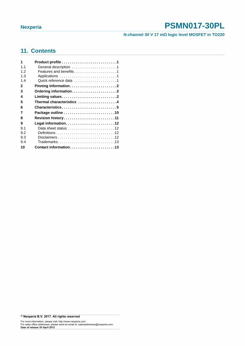
11. Contents
1 Product profile . . . . . . . . . . . . . . . . . . . . . . . . . . .11.1 General description . . . . . . . . . . . . . . . . . . . . . .11.2 Features and benefits . . . . . . . . . . . . . . . . . . . . .11.3 Applications . . . . . . . . . . . . . . . . . . . . . . . . . . . .11.4 Quick reference data . . . . . . . . . . . . . . . . . . . . .1
2 Pinning information. . . . . . . . . . . . . . . . . . . . . . .2
3 Ordering information. . . . . . . . . . . . . . . . . . . . . .2
4 Limiting values. . . . . . . . . . . . . . . . . . . . . . . . . . .2
5 Thermal characteristics . . . . . . . . . . . . . . . . . . .4
6 Characteristics. . . . . . . . . . . . . . . . . . . . . . . . . . .5
7 Package outline . . . . . . . . . . . . . . . . . . . . . . . . .10
8 Revision history. . . . . . . . . . . . . . . . . . . . . . . . . 11
9 Legal information. . . . . . . . . . . . . . . . . . . . . . . .129.1 Data sheet status . . . . . . . . . . . . . . . . . . . . . . .129.2 Definitions. . . . . . . . . . . . . . . . . . . . . . . . . . . . .129.3 Disclaimers . . . . . . . . . . . . . . . . . . . . . . . . . . . .129.4 Trademarks. . . . . . . . . . . . . . . . . . . . . . . . . . . .13
10 Contact information. . . . . . . . . . . . . . . . . . . . . .13
© Nexperia B.V. 2017. All rights reservedFor more information, please visit: http://www.nexperia.comFor sales office addresses, please send an email to: [email protected] Date of release: 03 April 2012