Production Solutions for Via Reveal - SEMI.ORG Production... · Production Solutions for Via Reveal...
18
©2012 SPTS Technologies - Confidential & Proprietary ©2012 SPTS Technologies - Confidential & Proprietary David Butler European 3D TSV Summit 2013 Production Solutions for Via Reveal
Transcript of Production Solutions for Via Reveal - SEMI.ORG Production... · Production Solutions for Via Reveal...

©2012 SPTS Technologies - Confidential & Proprietary ©2012 SPTS Technologies - Confidential & Proprietary
David Butler
European 3D TSV Summit 2013
Production Solutions for Via Reveal

2
This presentation and the information contained within it is the property of SPTS Technologies and is confidential. Any duplication, disclosure, distribution, dissemination or copying
of this presentation or its contents or use for any purpose other than that for which it is supplied is strictly prohibited, without the prior written consent of SPTS Technologies. © 2012 SPTS Technologies
■ New packaging space: “Mid-End”
■ Via reveal basics
■ Si reveal etch
■ Uniformity and depth control
■ Smoothness
■ ReVia – via reveal endpointing
■ Cu via passivation – PECVD oxide & nitride
■ Dealing with outgassing wafers
■ Low temperature oxide, stability challenge
■ Leakage & stress data for <180C TEOS
■ Oxide & nitride in one module
Contents

3
This presentation and the information contained within it is the property of SPTS Technologies and is confidential. Any duplication, disclosure, distribution, dissemination or copying
of this presentation or its contents or use for any purpose other than that for which it is supplied is strictly prohibited, without the prior written consent of SPTS Technologies. © 2012 SPTS Technologies
New Packaging Space: “Mid-End”
Front-end Back-end
IDM/foundry
Device fabrication
TSV creation
OSAT
Dicing
Wire-bonding
Assembly & package
Mid-end
IDM/Foundry or OSAT
Wafer thinning
Thin wafer handling
Backside processing
Micro-bumping/RDL
D2W stacking

4
This presentation and the information contained within it is the property of SPTS Technologies and is confidential. Any duplication, disclosure, distribution, dissemination or copying
of this presentation or its contents or use for any purpose other than that for which it is supplied is strictly prohibited, without the prior written consent of SPTS Technologies. © 2012 SPTS Technologies
Via Reveal
1. Finished TSV Wafer, Via first or middle
2. Flip wafer and bond to glass. Bulk grind Si to stop short of vias
Glass carrier
3. Plasma thin Si to expose base
of vias. Leave oxide sleeve intact 4. Dep nitride/oxide. CMP or dielectric
etch. Ready for RDL

5
This presentation and the information contained within it is the property of SPTS Technologies and is confidential. Any duplication, disclosure, distribution, dissemination or copying
of this presentation or its contents or use for any purpose other than that for which it is supplied is strictly prohibited, without the prior written consent of SPTS Technologies. © 2012 SPTS Technologies
■ Multiple operating modes
■ 2 x RF source powers
■ 1 x RF bias power
■ Dual gas inlet
■ Electro-static clamping
■ Wafers on carriers & stacks
■ Wafer edge protection option
■ End-point detection
Pegasus Rapier DRIE
‘RIE’ mode ‘ICP’ mode
‘DSi’ mode ‘Rapier’ mode
Original technology
Std decoupled source
Newer technology
Dual source
Newest technology

6
This presentation and the information contained within it is the property of SPTS Technologies and is confidential. Any duplication, disclosure, distribution, dissemination or copying
of this presentation or its contents or use for any purpose other than that for which it is supplied is strictly prohibited, without the prior written consent of SPTS Technologies. © 2012 SPTS Technologies
■ Before reveal, prior steps contribute to NU
■ TSV etch uniformity
■ Grinding uniformity
■ Use different etch modes of Rapier to adjust NU
2 Step Approach - Dealing with Incoming NU
Rapier DSi ‘RIE’
Edge fast Centre fast Uniform

7
This presentation and the information contained within it is the property of SPTS Technologies and is confidential. Any duplication, disclosure, distribution, dissemination or copying
of this presentation or its contents or use for any purpose other than that for which it is supplied is strictly prohibited, without the prior written consent of SPTS Technologies. © 2012 SPTS Technologies
TSV wafer
Successful stop on
~200nm liner oxide
Clean Si
surfaces
■ Si etch rate up to 6 µm/min
■ <3% non-unif, 3mm EE
■ 165:1 selectivity to oxide
■ Av roughness added <5Å
Via Reveal Etch

8
This presentation and the information contained within it is the property of SPTS Technologies and is confidential. Any duplication, disclosure, distribution, dissemination or copying
of this presentation or its contents or use for any purpose other than that for which it is supplied is strictly prohibited, without the prior written consent of SPTS Technologies. © 2012 SPTS Technologies
The Need for Endpoint
After grind, uncertain Si
thickness above via No Endpoint… With Endpoint…
Si etch with Endpoint
Next step
No rework. $$$
saved
Every wafer will be different.
Rework common. $$$ lost
Timed Si etch
Offline. Profilometer
Via revealed?
Next step
More etch
SCRAP

9
This presentation and the information contained within it is the property of SPTS Technologies and is confidential. Any duplication, disclosure, distribution, dissemination or copying
of this presentation or its contents or use for any purpose other than that for which it is supplied is strictly prohibited, without the prior written consent of SPTS Technologies. © 2012 SPTS Technologies
■ Detects to 0.01% open area
ReVia™ Si Etch Endpoint
5 consecutive wafers
Nominally identical
Time
Variable end-point due
to differing grind
thicknesses of Si

©2012 SPTS Technologies - Confidential & Proprietary ©2012 SPTS Technologies - Confidential & Proprietary
Via Reveal Dielectrics

11
This presentation and the information contained within it is the property of SPTS Technologies and is confidential. Any duplication, disclosure, distribution, dissemination or copying
of this presentation or its contents or use for any purpose other than that for which it is supplied is strictly prohibited, without the prior written consent of SPTS Technologies. © 2012 SPTS Technologies
Adv Packaging. Wafers Outgas
■ Next gen packaging wafers are a challenge for plasma processes
■ Si on tape, or thinned and temporarily bonded to glass
■ Contain moisture/solvent, BUT low temperature constraint
■ Debond, or bow if wafers overheated
■ Long degas times required = slow throughput
Contamination will
degrade film quality
Degas needs to be done
inside PECVD system

12
This presentation and the information contained within it is the property of SPTS Technologies and is confidential. Any duplication, disclosure, distribution, dissemination or copying
of this presentation or its contents or use for any purpose other than that for which it is supplied is strictly prohibited, without the prior written consent of SPTS Technologies. © 2012 SPTS Technologies
■ 75 wafer batch vacuum degas module
■ Low temperature, long degas
■ No thermal shock for SoG
■ No delamination of bonding adhesive
Comparison
■ 15 min degas per wafer, <150C
■ No throughput loss with batch degas
■ 4x lower t’put with single wafer degas
Batch Degas on DCVD Systems

13
This presentation and the information contained within it is the property of SPTS Technologies and is confidential. Any duplication, disclosure, distribution, dissemination or copying
of this presentation or its contents or use for any purpose other than that for which it is supplied is strictly prohibited, without the prior written consent of SPTS Technologies. © 2012 SPTS Technologies
■ FTIR shows water absorption over time
■ Electrical leakage increases
■ Refractive Index increases
■ Unusable for 2.5D/3D packaging
■ Don’t trust ‘Day 1’ data !
“Standard” LT TEOS is not Stable
Water
Absorption
Si-O
OH
Leakage
Increase
14
This presentation and the information contained within it is the property of SPTS Technologies and is confidential. Any duplication, disclosure, distribution, dissemination or copying
of this presentation or its contents or use for any purpose other than that for which it is supplied is strictly prohibited, without the prior written consent of SPTS Technologies. © 2012 SPTS Technologies
■ Unique low temperature PE-TEOS SiO
■ Unique process chemistry and post-deposition treatment
■ Multiple patent applications
■ Stable electrical properties and film stress
■ No drift in film properties over time
■ No water absorption on exposure to atmosphere
Electrically Stable LT TEOS Films
Leakage current vs Electric
field for SPTS LT TEOS SiO,
measured as-deposited and
after 2 & 9 days.
TEOS SiO: TWAFER MAX <180°C

15
This presentation and the information contained within it is the property of SPTS Technologies and is confidential. Any duplication, disclosure, distribution, dissemination or copying
of this presentation or its contents or use for any purpose other than that for which it is supplied is strictly prohibited, without the prior written consent of SPTS Technologies. © 2012 SPTS Technologies
■ No change in TEOS SiO stress over time
■ Critical for bow compensation
■ Compressive and tensile SiO films available
…And Stable Stress
TEOS SiO: TWAFER MAX <180°C
Stress vs Time

16
This presentation and the information contained within it is the property of SPTS Technologies and is confidential. Any duplication, disclosure, distribution, dissemination or copying
of this presentation or its contents or use for any purpose other than that for which it is supplied is strictly prohibited, without the prior written consent of SPTS Technologies. © 2012 SPTS Technologies
■ SiN/SiO over 10µm Ø TSV, with ~5µm revealed
<180C SiN-SiO on Revealed TSV
■ 300mm wafers
■ SiN & SiO deposited in same chamber
■ No voids or seams
■ Stress < 200 MPa
■ Low leakage, high breakdown
■ Stable leakage – no change over time
■ No adhesion failures
0.1µm SiN +
2.7µm SiO
2.3µm SiN
TEOS SiO Deposited at <180°C [wafer temp]
17
This presentation and the information contained within it is the property of SPTS Technologies and is confidential. Any duplication, disclosure, distribution, dissemination or copying
of this presentation or its contents or use for any purpose other than that for which it is supplied is strictly prohibited, without the prior written consent of SPTS Technologies. © 2012 SPTS Technologies
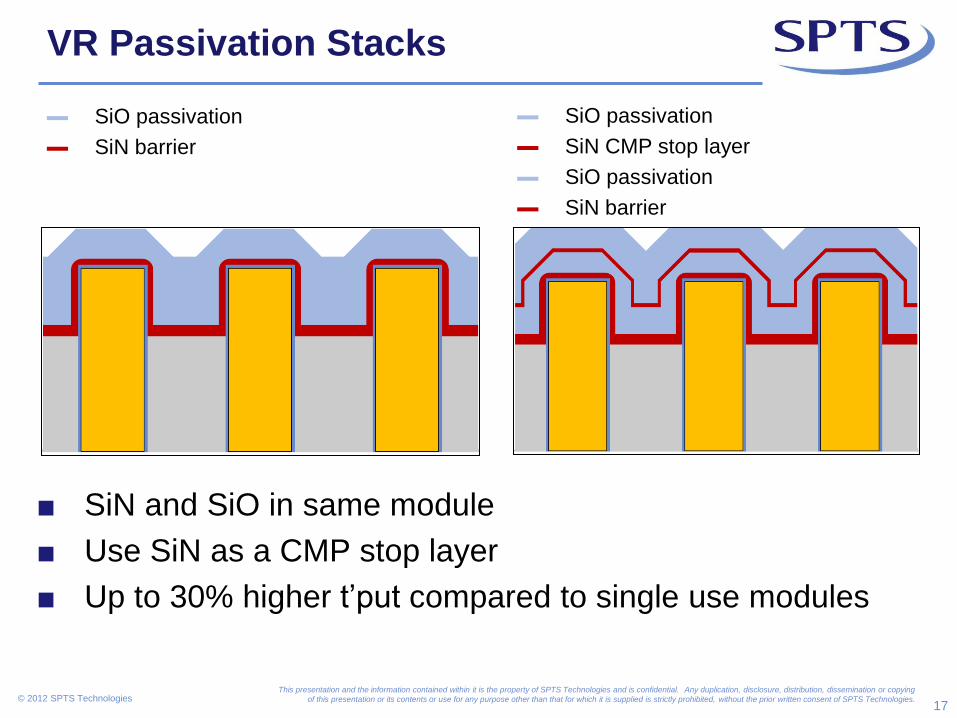
▬ SiO passivation
▬ SiN barrier
VR Passivation Stacks
▬ SiO passivation
▬ SiN CMP stop layer
▬ SiO passivation
▬ SiN barrier
■ SiN and SiO in same module
■ Use SiN as a CMP stop layer
■ Up to 30% higher t’put compared to single use modules

18
This presentation and the information contained within it is the property of SPTS Technologies and is confidential. Any duplication, disclosure, distribution, dissemination or copying
of this presentation or its contents or use for any purpose other than that for which it is supplied is strictly prohibited, without the prior written consent of SPTS Technologies. © 2012 SPTS Technologies
■ Low temperature solutions for via reveal
■ Multi mode etch module
■ Different modes to offset pre-reveal non-uniformity
■ High rate, highly uniform, high selectivity Si etches
■ Unique endpoint
■ <180°C SiN and SiO dielectrics
■ Low temp nitride and TEOS oxide in one module
■ Degas for problem substrates
■ Low leakage and high breakdown voltage
■ Seamless coverage over Cu nodes
■ Dedicated systems, or on the same platform
Summary