Process Performance of Silicon Thin-Film Transfer Using ...
10
1 Copyright © 2014 by ASME PROCESS PERFORMANCE OF SILICON THIN-FILM TRANSFER USING LASER MICRO-TRANSFER PRINTING Ala’a Al-okaily Mechanical Science and Engineering Department University of Illinois at Urbana-Champaign Urbana, IL, USA [email protected] Placid Ferreira Mechanical Science and Engineering Department University of Illinois at Urbana-Champaign Urbana, IL, USA [email protected] ABSTRACT Micro-transfer printing is rapidly emerging as an effective pathway for heterogeneous materials integration. The process transfers pre-fabricated micro- and nano-scale structures, referred to as “ink,” from growth donor substrates to functional receiving substrates. As a non-contact pattern transfer method, Laser Micro-Transfer Printing (LMTP) has been introduced to enhance the capabilities of transfer printing technology to be independent of the receiving substrate material, geometry, and preparation. Using micro fabricated square silicon as inks and polydimethylsiloxane (PDMS) as the stamp material. The previous work on the LMTP process focused on experimentally characterizing and modeling the effects of transferred inks’ sizes and thicknesses, and laser beam powers on the laser-driven delamination process mechanism. In this paper, several studies are conducted to understand the effects of other process parameters such as stamp post dimensions (size and height), PDMS formulation for the stamp, ink-stamp alignment, and the shape of the transferred silicon inks on the LMTP performance and mechanism. The studies are supported by both experimental data for the laser pulse duration required to initiate the delamination, and thermo-mechanical FEA model predictions of the energy stored at the interface’s edges to release the ink (Energy Release Rate (ERR)), stress levels at the delamination crack tip (Stress Intensity Factors (SIFs)), and interfacial temperature. This study, along with previous studies, should help LMTP users to understand the effects of the process parameters on the process performance so as to select optimal operation conditions. NOMENCLATURE A a Area of an aperture that has same ink dimensions h s Thickness of silicon ink h p Height of PDMS stamp post I a Intensity of laser beam on ink surface L s Size of square silicon ink L s Size of square PDMS stamp post P a Power of laser beam incident on the ink (P a = A a I a ) P b Power of laser beam absorbed by ink P i Power absorbed by the ink on the i th internally reflected pass R Ratio of post to ink size R B Reflectivity of silicon ink’s bottom surface R T Reflectivity of silicon ink’s top surface α Optical absorption coefficient of silicon INTRODUCTION Heterogeneous materials integration, motivated by pattern transfer processes, has evolved to address the technology gap between the conventional micro-fabrication processes and multi-layer functional device integration. Since thin-film non- contact release is difficult to achieve at the micro-scale (surface effects dominate), pattern release has always been a challenge and that is dependent on the receiving substrate properties and preparation. Micro-transfer printing, due to it is simplicity, accuracy, and large-scale materials integration capabilities, is rapidly emerging as an effective pathway for flexible and stretchable functional device integration (examples are shown in Fig. 1 [1]). As a contact pattern transfer process, micro- transfer printing uses a simple patterned stamp, usually made out of polydimethylsiloxane (PDMS), as a tool to selectively pick-up pattern from a dense array of under-cut and ready-to- pick micro-structures, referred to as “ink,” utilizing Van der Waals forces between the ink and the stamp. The inks are then released by modulating the adhesion strength of the strain rate dependent viscoelastic-elastic interface, at the ink-stamp interface, by controlling the stamp retraction velocity [2]. Several modifications have been introduced to print on low adhesion surfaces. Engineering the stamp (patterned stamps [3], pedestal-shaped stamps [4], and microtipped stamps [5]) or enhancing the release mechanism (shear-enhanced [6] and fluidic-chamber actuated stamps [7]) are prescriptive of such efforts. Proceedings of the ASME 2014 International Mechanical Engineering Congress and Exposition IMECE2014 November 14-20, 2014, Montreal, Quebec, Canada IMECE2014-37133
Transcript of Process Performance of Silicon Thin-Film Transfer Using ...
1 Copyright © 2014 by ASME
PROCESS PERFORMANCE OF SILICON THIN-FILM TRANSFER USING LASER MICRO-TRANSFER PRINTING
Ala’a Al-okaily Mechanical Science and Engineering Department
University of Illinois at Urbana-Champaign Urbana, IL, USA
Placid Ferreira Mechanical Science and Engineering Department
University of Illinois at Urbana-Champaign Urbana, IL, USA
ABSTRACT Micro-transfer printing is rapidly emerging as an effective
pathway for heterogeneous materials integration. The process
transfers pre-fabricated micro- and nano-scale structures,
referred to as “ink,” from growth donor substrates
to functional receiving substrates. As a non-contact pattern
transfer method, Laser Micro-Transfer Printing (LMTP) has
been introduced to enhance the capabilities of transfer printing
technology to be independent of the receiving substrate
material, geometry, and preparation. Using micro fabricated
square silicon as inks and polydimethylsiloxane (PDMS) as the
stamp material. The previous work on the LMTP process
focused on experimentally characterizing and modeling the
effects of transferred inks’ sizes and thicknesses, and laser
beam powers on the laser-driven delamination process
mechanism. In this paper, several studies are conducted to
understand the effects of other process parameters such as
stamp post dimensions (size and height), PDMS formulation for
the stamp, ink-stamp alignment, and the shape of the
transferred silicon inks on the LMTP performance and
mechanism. The studies are supported by both experimental
data for the laser pulse duration required to initiate the
delamination, and thermo-mechanical FEA model predictions
of the energy stored at the interface’s edges to release the ink
(Energy Release Rate (ERR)), stress levels at the delamination
crack tip (Stress Intensity Factors (SIFs)), and interfacial
temperature. This study, along with previous studies, should
help LMTP users to understand the effects of the process
parameters on the process performance so as to select optimal
operation conditions.
NOMENCLATURE Aa Area of an aperture that has same ink dimensions
hs Thickness of silicon ink
hp Height of PDMS stamp post
Ia Intensity of laser beam on ink surface
Ls Size of square silicon ink
Ls Size of square PDMS stamp post
Pa Power of laser beam incident on the ink (Pa = Aa Ia)
Pb Power of laser beam absorbed by ink
Pi Power absorbed by the ink on the ith
internally
reflected pass
R Ratio of post to ink size
RB Reflectivity of silicon ink’s bottom surface
RT Reflectivity of silicon ink’s top surface
α Optical absorption coefficient of silicon
INTRODUCTION Heterogeneous materials integration, motivated by pattern
transfer processes, has evolved to address the technology gap
between the conventional micro-fabrication processes and
multi-layer functional device integration. Since thin-film non-
contact release is difficult to achieve at the micro-scale (surface
effects dominate), pattern release has always been a challenge
and that is dependent on the receiving substrate properties and
preparation. Micro-transfer printing, due to it is simplicity,
accuracy, and large-scale materials integration capabilities, is
rapidly emerging as an effective pathway for flexible and
stretchable functional device integration (examples are shown
in Fig. 1 [1]). As a contact pattern transfer process, micro-
transfer printing uses a simple patterned stamp, usually made
out of polydimethylsiloxane (PDMS), as a tool to selectively
pick-up pattern from a dense array of under-cut and ready-to-
pick micro-structures, referred to as “ink,” utilizing Van der
Waals forces between the ink and the stamp. The inks are then
released by modulating the adhesion strength of the strain rate
dependent viscoelastic-elastic interface, at the ink-stamp
interface, by controlling the stamp retraction velocity [2].
Several modifications have been introduced to print on low
adhesion surfaces. Engineering the stamp (patterned stamps [3],
pedestal-shaped stamps [4], and microtipped stamps [5]) or
enhancing the release mechanism (shear-enhanced [6] and
fluidic-chamber actuated stamps [7]) are prescriptive of such
efforts.
Proceedings of the ASME 2014 International Mechanical Engineering Congress and Exposition IMECE2014
November 14-20, 2014, Montreal, Quebec, Canada
IMECE2014-37133
2 Copyright © 2014 by ASME
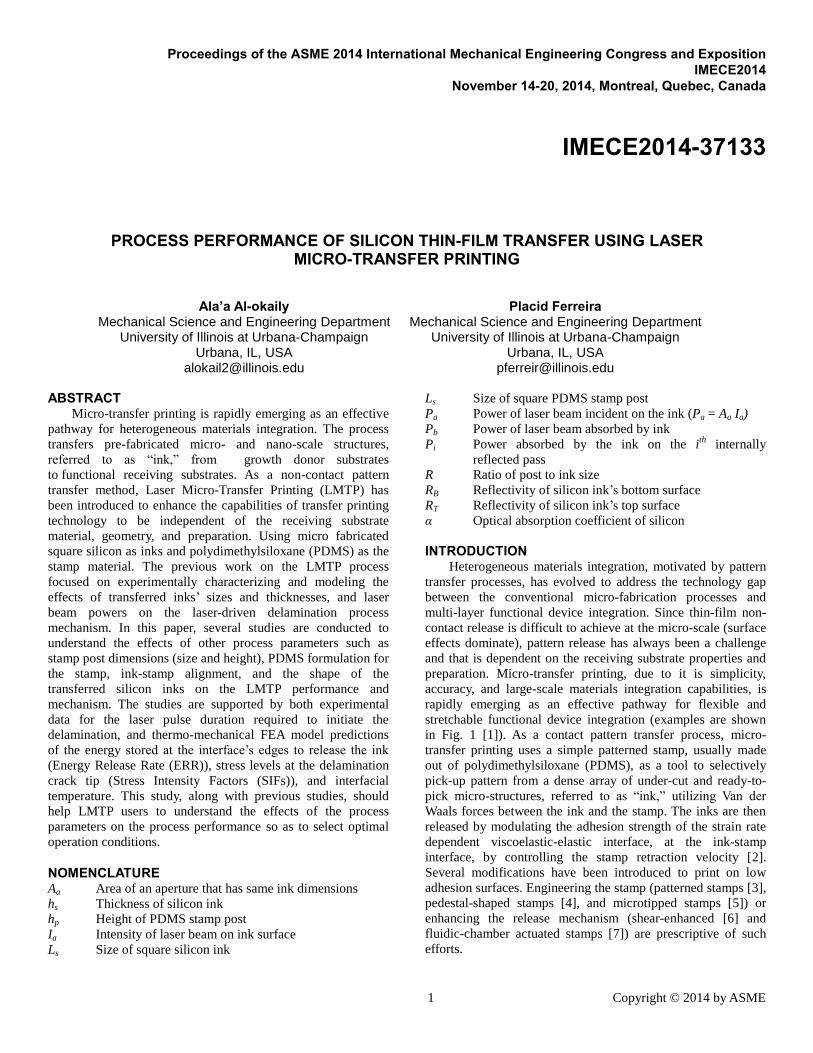
Figure 1 . Examples of uncommon constructs, devices and
integrated systems realized by micro transfer printing. (a) SEM
image of a printed multilayer stack of silicon platelets. (b)
Photograph of a large area (10 x10 cm) negative index
metamaterial (NIM) comprised of alternating layers of Ag and
MgF2 in a nano-scale fishnet pattern printed onto a flexible
substrate. (c) Photograph of an ‘epidermal’ electronic device,
conformally laminated onto the surface of the skin. (d) Image
of a mechanically flexed array of ultrathin, micro-scale, blue
LEDs printed from a source wafer onto a thin strip of plastic.
(e) Picture of a 4-inch, full-color quantum dot (QD) LED
display. (f) Photograph of a flexible integrated circuit that uses
printed networks of single walled carbon nanotubes for the
semiconductor. (Composite figure taken from [1]).
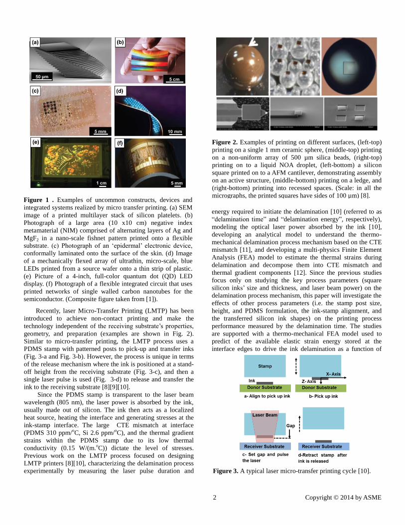
Figure 3. A typical laser micro-transfer printing cycle [10].
Figure 2. Examples of printing on different surfaces, (left-top)
printing on a single 1 mm ceramic sphere, (middle-top) printing
on a non-uniform array of 500 µm silica beads, (right-top)
printing on to a liquid NOA droplet, (left-bottom) a silicon
square printed on to a AFM cantilever, demonstrating assembly
on an active structure, (middle-bottom) printing on a ledge, and
(right-bottom) printing into recessed spaces. (Scale: in all the
micrographs, the printed squares have sides of 100 µm) [8].
Recently, laser Micro-Transfer Printing (LMTP) has been
introduced to achieve non-contact printing and make the
technology independent of the receiving substrate’s properties,
geometry, and preparation (examples are shown in Fig. 2).
Similar to micro-transfer printing, the LMTP process uses a
PDMS stamp with patterned posts to pick-up and transfer inks
(Fig. 3-a and Fig. 3-b). However, the process is unique in terms
of the release mechanism where the ink is positioned at a stand-
off height from the receiving substrate (Fig. 3-c), and then a
single laser pulse is used (Fig. 3-d) to release and transfer the
ink to the receiving substrate [8][9][10].
Since the PDMS stamp is transparent to the laser beam
wavelength (805 nm), the laser power is absorbed by the ink,
usually made out of silicon. The ink then acts as a localized
heat source, heating the interface and generating stresses at the
ink-stamp interface. The large CTE mismatch at interface
(PDMS 310 ppm/oC, Si 2.6 ppm/
oC), and the thermal gradient
strains within the PDMS stamp due to its low thermal
conductivity (0.15 W/(m.oC)) dictate the level of stresses.
Previous work on the LMTP process focused on designing
LMTP printers [8][10], characterizing the delamination process
experimentally by measuring the laser pulse duration and
energy required to initiate the delamination [10] (referred to as
“delamination time” and “delamination energy”, respectively),
modeling the optical laser power absorbed by the ink [10],
developing an analytical model to understand the thermo-
mechanical delamination process mechanism based on the CTE
mismatch [11], and developing a multi-physics Finite Element
Analysis (FEA) model to estimate the thermal strains during
delamination and decompose them into CTE mismatch and
thermal gradient components [12]. Since the previous studies
focus only on studying the key process parameters (square
silicon inks’ size and thickness, and laser beam power) on the
delamination process mechanism, this paper will investigate the
effects of other process parameters (i.e. the stamp post size,
height, and PDMS formulation, the ink-stamp alignment, and
the transferred silicon ink shapes) on the printing process
performance measured by the delamination time. The studies
are supported with a thermo-mechanical FEA model used to
predict of the available elastic strain energy stored at the
interface edges to drive the ink delamination as a function of
3 Copyright © 2014 by ASME
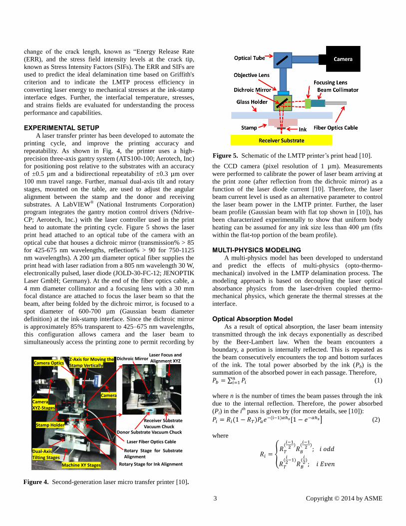
Figure 4. Second-generation laser micro transfer printer [10].
-
-
-
Figure 5. Schematic of the LMTP printer’s print head [10].
change of the crack length, known as “Energy Release Rate
(ERR), and the stress field intensity levels at the crack tip,
known as Stress Intensity Factors (SIFs). The ERR and SIFs are
used to predict the ideal delamination time based on Griffith's
criterion and to indicate the LMTP process efficiency in
converting laser energy to mechanical stresses at the ink-stamp
interface edges. Further, the interfacial temperature, stresses,
and strains fields are evaluated for understanding the process
performance and capabilities.
EXPERIMENTAL SETUP A laser transfer printer has been developed to automate the
printing cycle, and improve the printing accuracy and
repeatability. As shown in Fig. 4, the printer uses a high-
precision three-axis gantry system (ATS100-100; Aerotech, Inc)
for positioning post relative to the substrates with an accuracy
of ±0.5 µm and a bidirectional repeatability of ±0.3 µm over
100 mm travel range. Further, manual dual-axis tilt and rotary
stages, mounted on the table, are used to adjust the angular
alignment between the stamp and the donor and receiving
substrates. A LabVIEW® (National Instruments Corporation)
program integrates the gantry motion control drivers (Ndrive-
CP; Aerotech, Inc.) with the laser controller used in the print
head to automate the printing cycle. Figure 5 shows the laser
print head attached to an optical tube of the camera with an
optical cube that houses a dichroic mirror (transmission% > 85
for 425-675 nm wavelengths, reflection% > 90 for 750-1125
nm wavelengths). A 200 µm diameter optical fiber supplies the
print head with laser radiation from a 805 nm wavelength 30 W,
electronically pulsed, laser diode (JOLD-30-FC-12; JENOPTIK
Laser GmbH; Germany). At the end of the fiber optics cable, a
4 mm diameter collimator and a focusing lens with a 30 mm
focal distance are attached to focus the laser beam so that the
beam, after being folded by the dichroic mirror, is focused to a
spot diameter of 600-700 µm (Gaussian beam diameter
definition) at the ink-stamp interface. Since the dichroic mirror
is approximately 85% transparent to 425–675 nm wavelengths,
this configuration allows camera and the laser beam to
simultaneously access the printing zone to permit recording by
the CCD camera (pixel resolution of 1 µm). Measurements
were performed to calibrate the power of laser beam arriving at
the print zone (after reflection from the dichroic mirror) as a
function of the laser diode current [10]. Therefore, the laser
beam current level is used as an alternative parameter to control
the laser beam power in the LMTP printer. Further, the laser
beam profile (Gaussian beam with flat top shown in [10]), has
been characterized experimentally to show that uniform body
heating can be assumed for any ink size less than 400 μm (fits
within the flat-top portion of the beam profile).
MULTI-PHYSICS MODELING A multi-physics model has been developed to understand
and predict the effects of multi-physics (opto-thermo-
mechanical) involved in the LMTP delamination process. The
modeling approach is based on decoupling the laser optical
absorbance physics from the laser-driven coupled thermo-
mechanical physics, which generate the thermal stresses at the
interface.
Optical Absorption Model As a result of optical absorption, the laser beam intensity
transmitted through the ink decays exponentially as described
by the Beer-Lambert law. When the beam encounters a
boundary, a portion is internally reflected. This is repeated as
the beam consecutively encounters the top and bottom surfaces
of the ink. The total power absorbed by the ink (Pb) is the
summation of the absorbed power in each passage. Therefore,
𝑃𝑏 = ∑ 𝑃𝑖𝑛𝑖=1 (1)
where n is the number of times the beam passes through the ink
due to the internal reflection. Therefore, the power absorbed
(Pi) in the ith
pass is given by (for more details, see [10]):
𝑃𝑖 = 𝑅𝑖(1 − 𝑅𝑇)𝑃𝑎𝑒−(i−1)𝛼ℎ [1 − 𝑒−𝛼ℎ ] (2)
where
𝑅𝑖 = {𝑅𝑇
(𝑖−12
)𝑅𝐵
(𝑖−12
); 𝑖 𝑜𝑑𝑑
𝑅𝑇
(𝑖2−1)
𝑅𝐵
(𝑖2); 𝑖 𝐸𝑣𝑒𝑛
4 Copyright © 2014 by ASME
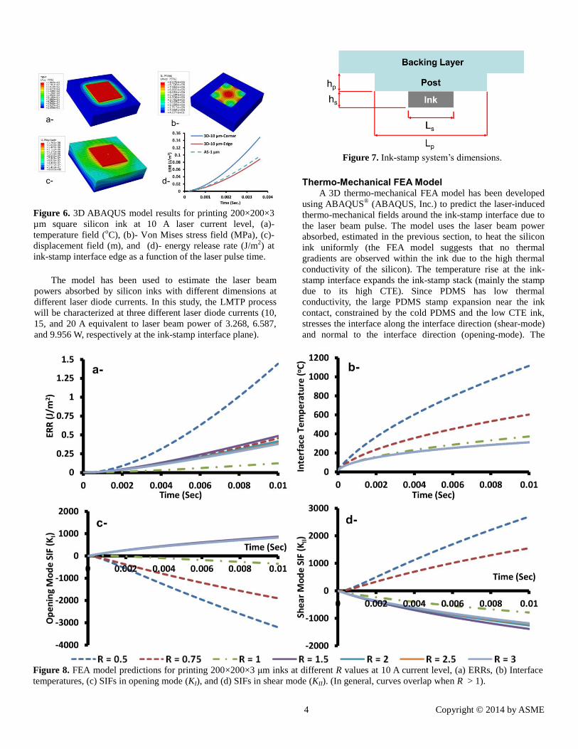
Figure 6. 3D ABAQUS model results for printing 200×200×3
µm square silicon ink at 10 A laser current level, (a)-
temperature field (oC), (b)- Von Mises stress field (MPa), (c)-
displacement field (m), and (d)- energy release rate (J/m2) at
ink-stamp interface edge as a function of the laser pulse time.
Figure 7. Ink-stamp system’s dimensions.
Figure 8. FEA model predictions for printing 200×200×3 μm inks at different R values at 10 A current level, (a) ERRs, (b) Interface
temperatures, (c) SIFs in opening mode (KI), and (d) SIFs in shear mode (KII). (In general, curves overlap when R > 1).
The model has been used to estimate the laser beam
powers absorbed by silicon inks with different dimensions at
different laser diode currents. In this study, the LMTP process
will be characterized at three different laser diode currents (10,
15, and 20 A equivalent to laser beam power of 3.268, 6.587,
and 9.956 W, respectively at the ink-stamp interface plane).
Thermo-Mechanical FEA Model A 3D thermo-mechanical FEA model has been developed
using ABAQUS® (ABAQUS, Inc.) to predict the laser-induced
thermo-mechanical fields around the ink-stamp interface due to
the laser beam pulse. The model uses the laser beam power
absorbed, estimated in the previous section, to heat the silicon
ink uniformly (the FEA model suggests that no thermal
gradients are observed within the ink due to the high thermal
conductivity of the silicon). The temperature rise at the ink-
stamp interface expands the ink-stamp stack (mainly the stamp
due to its high CTE). Since PDMS has low thermal
conductivity, the large PDMS stamp expansion near the ink
contact, constrained by the cold PDMS and the low CTE ink,
stresses the interface along the interface direction (shear-mode)
and normal to the interface direction (opening-mode). The
5 Copyright © 2014 by ASME
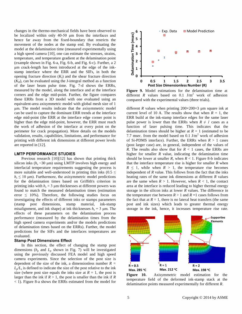
Figure 9. Model estimations for the delamination time at
different R values based on 0.1 J/m2 work of adhesion
compared with the experimental values (three trials).
Figure 10. Axisymmetric model estimation for the
temperature field of the deformed ink-stamp stack at the
delamination points measured experimentally for different R.
changes in the thermo-mechanical fields have been observed to
be localized within only 40-50 μm from the interfaces and
hence far away from the fixed-boundary that restricts the
movement of the nodes at the stamp end. By evaluating the
model at the delamination time (measured experimentally using
a high speed camera [10], one can estimate the stresses, strains,
temperature, and temperature gradient at the delamination point
(example shown in Fig. 6-a, Fig. 6-b, and Fig. 6-c). Further, a 2
μm crack-length has been introduced at the edge of the ink-
stamp interface where the ERR and the SIFs, in both the
opening fracture direction (KI) and the shear fracture direction
(KII), can be evaluated using the J-integral method as a function
of the laser beam pulse time. Fig. 7-d shows the ERRs,
measured by the model, along the interface and at the interface
corners and the edge mid-point. Further, the figure compares
these ERRs from a 3D model with one evaluated using an
equivalent-area axisymmetric model with global mesh size of 1
μm. The model results indicate that the axisymmetric model
can be used to capture the dominant ERR trends at the interface
edge mid-point (the ERR at the interface edge corner point is
higher than the edge mid-point, however, the ERR must reach
the work of adhesion of the interface at every point on the
perimeter for crack propagation). More details on the models
validation, results, capabilities, limitations, and performance for
printing with different ink dimensions at different power levels
are reported in [12].
LMTP PERFORMANCE STUDIES Previous research [10][12] has shown that printing thick
silicon inks (hs ~30 μm) using LMTP involves high energy and
interfacial temperature requirements suggesting the process is
more suitable and well-understood in printing thin inks (0.5 ≤
hs ≤ 10 μm). Furthermore, the axisymmetric model predictions
for the delamination times based on Griffith's criterion in
printing inks with hs = 3 μm thicknesses at different powers was
found to match the measured delamination times (estimation
error ≤ 10%). Therefore, the following studies focus on
investigating the effects of different inks or stamps parameters
(stamp post dimensions, stamp material, ink-stamp
misalignment, and ink shape) at ink thicknesses hs = 3 μm. The
effects of these parameters on the delamination process
performance (measured by the delamination times from the
high speed camera experiments and/or the models predictions
of delamination times based on the ERRs). Further, the model
predictions for the SIFs and the interfaces temperatures are
evaluated.
Stamp Post Dimensions Effect In this section, the effect of changing the stamp post
dimensions (hp and Lp shown in Fig. 7) will be investigated
using the previously discussed FEA model and high speed
camera experiments. Since the selection of the post size is
dependent of the size of the ink, a dimensionless number R =
Lp/Ls is defined to indicate the size of the post relative to the ink
size (where post size equals the inks size at R = 1, the post is
larger than the ink if R > 1, the post is smaller than the ink if R
< 1). Figure 8-a shows the ERRs estimated from the model for
different R values when printing 200×200×3 µm square ink at
current level of 10 A. The results show that when R = 1, the
ERR build at the ink-stamp interface edges for the same laser
pulse power is lower than the ERRs when R ≠ 1 cases as a
function of laser pulsing time. This indicates that the
delamination times should be higher at R = 1 (estimated to be
7.7 msec. from the model based on 0.1 J/m2 work of adhesion
of Si-PDMS interface). Further, the ERRs when R > 1 cases
(post larger case) are, in general, independent of the values of
R. The results also show that for R < 1 cases, the ERRs are
higher for smaller R value, indicating the delamination time
should be lower at smaller R, when R < 1. Figure 8-b indicates
that the interface temperature rise is higher for smaller R when
R ≤ 1, while when R > 1, the temperature rise becomes
independent of R value. This follows from the fact that the inks
heating rates of the same ink dimensions at different R values
are the same when R > 1. However, when R < 1, the contact
area at the interface is reduced leading to higher thermal energy
storage in the silicon inks at lower R values. The difference in
the temperature rise between R > 1 and R =1 cases follows from
the fact that at R = 1, there is no lateral heat transfers (the same
post and ink sizes) which leads to greater thermal energy
storage in the ink, hence, it increases temperature rise rate.
6 Copyright © 2014 by ASME
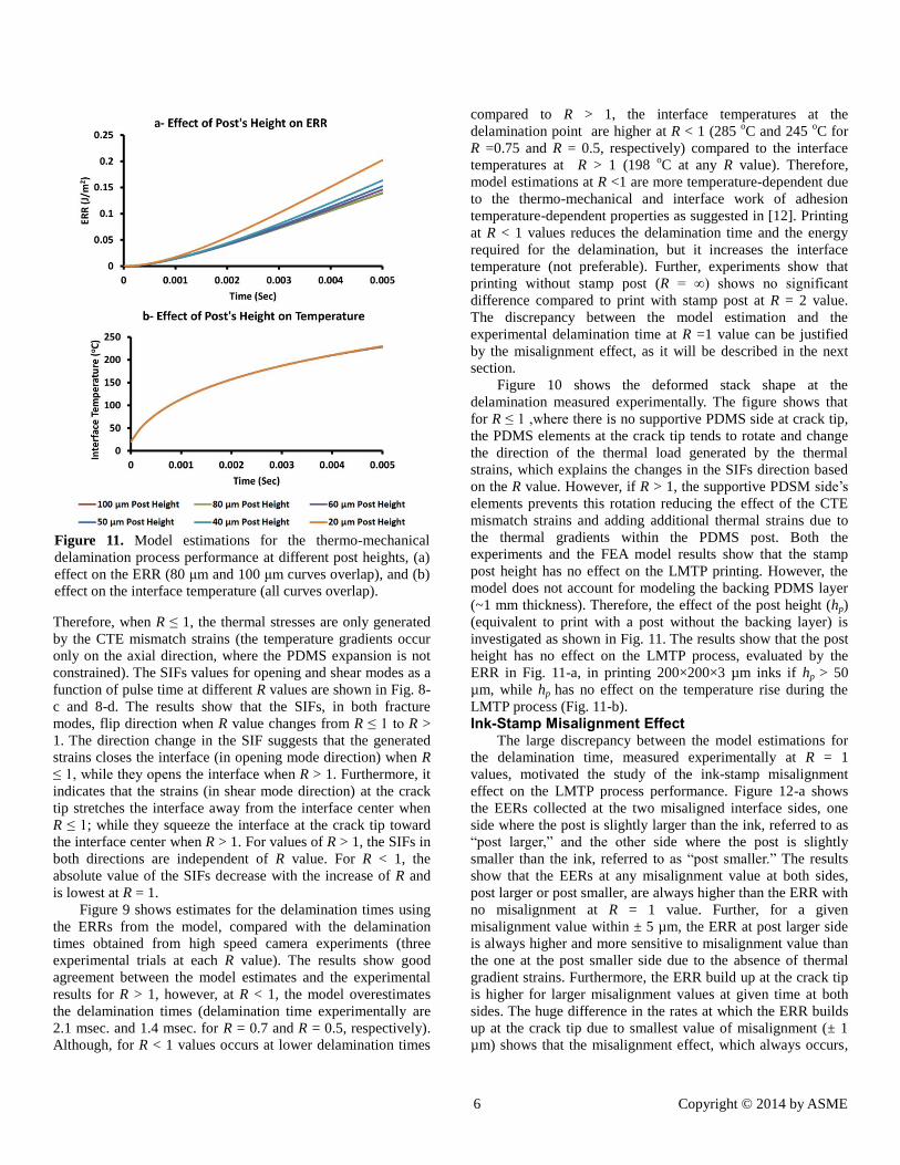
Figure 11. Model estimations for the thermo-mechanical
delamination process performance at different post heights, (a)
effect on the ERR (80 μm and 100 μm curves overlap), and (b)
effect on the interface temperature (all curves overlap).
. Therefore, when R ≤ 1, the thermal stresses are only generated
by the CTE mismatch strains (the temperature gradients occur
only on the axial direction, where the PDMS expansion is not
constrained). The SIFs values for opening and shear modes as a
function of pulse time at different R values are shown in Fig. 8-
c and 8-d. The results show that the SIFs, in both fracture
modes, flip direction when R value changes from R ≤ 1 to R >
1. The direction change in the SIF suggests that the generated
strains closes the interface (in opening mode direction) when R
≤ 1, while they opens the interface when R > 1. Furthermore, it
indicates that the strains (in shear mode direction) at the crack
tip stretches the interface away from the interface center when
R ≤ 1; while they squeeze the interface at the crack tip toward
the interface center when R > 1. For values of R > 1, the SIFs in
both directions are independent of R value. For R < 1, the
absolute value of the SIFs decrease with the increase of R and
is lowest at R = 1.
Figure 9 shows estimates for the delamination times using
the ERRs from the model, compared with the delamination
times obtained from high speed camera experiments (three
experimental trials at each R value). The results show good
agreement between the model estimates and the experimental
results for R > 1, however, at R < 1, the model overestimates
the delamination times (delamination time experimentally are
2.1 msec. and 1.4 msec. for R = 0.7 and R = 0.5, respectively).
Although, for R < 1 values occurs at lower delamination times
compared to R > 1, the interface temperatures at the
delamination point are higher at R < 1 (285 oC and 245
oC for
R =0.75 and R = 0.5, respectively) compared to the interface
temperatures at R > 1 (198 oC at any R value). Therefore,
model estimations at R <1 are more temperature-dependent due
to the thermo-mechanical and interface work of adhesion
temperature-dependent properties as suggested in [12]. Printing
at R < 1 values reduces the delamination time and the energy
required for the delamination, but it increases the interface
temperature (not preferable). Further, experiments show that
printing without stamp post (R = ∞) shows no significant
difference compared to print with stamp post at R = 2 value.
The discrepancy between the model estimation and the
experimental delamination time at R =1 value can be justified
by the misalignment effect, as it will be described in the next
section.
Figure 10 shows the deformed stack shape at the
delamination measured experimentally. The figure shows that
for R ≤ 1 ,where there is no supportive PDMS side at crack tip,
the PDMS elements at the crack tip tends to rotate and change
the direction of the thermal load generated by the thermal
strains, which explains the changes in the SIFs direction based
on the R value. However, if R > 1, the supportive PDSM side’s
elements prevents this rotation reducing the effect of the CTE
mismatch strains and adding additional thermal strains due to
the thermal gradients within the PDMS post. Both the
experiments and the FEA model results show that the stamp
post height has no effect on the LMTP printing. However, the
model does not account for modeling the backing PDMS layer
(~1 mm thickness). Therefore, the effect of the post height (hp)
(equivalent to print with a post without the backing layer) is
investigated as shown in Fig. 11. The results show that the post
height has no effect on the LMTP process, evaluated by the
ERR in Fig. 11-a, in printing 200×200×3 µm inks if hp > 50
µm, while hp has no effect on the temperature rise during the
LMTP process (Fig. 11-b). Ink-Stamp Misalignment Effect
The large discrepancy between the model estimations for
the delamination time, measured experimentally at R = 1
values, motivated the study of the ink-stamp misalignment
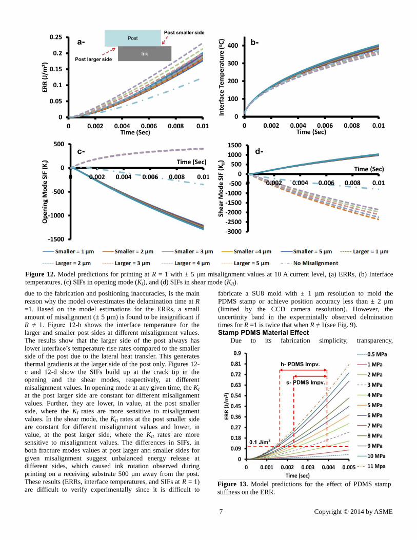
effect on the LMTP process performance. Figure 12-a shows
the EERs collected at the two misaligned interface sides, one
side where the post is slightly larger than the ink, referred to as
“post larger,” and the other side where the post is slightly
smaller than the ink, referred to as “post smaller.” The results
show that the EERs at any misalignment value at both sides,
post larger or post smaller, are always higher than the ERR with
no misalignment at R = 1 value. Further, for a given
misalignment value within ± 5 µm, the ERR at post larger side
is always higher and more sensitive to misalignment value than
the one at the post smaller side due to the absence of thermal
gradient strains. Furthermore, the ERR build up at the crack tip
is higher for larger misalignment values at given time at both
sides. The huge difference in the rates at which the ERR builds
up at the crack tip due to smallest value of misalignment (± 1
µm) shows that the misalignment effect, which always occurs,
7 Copyright © 2014 by ASME
Figure 13. Model predictions for the effect of PDMS stamp
stiffness on the ERR.
Figure 12. Model predictions for printing at R = 1 with ± 5 μm misalignment values at 10 A current level, (a) ERRs, (b) Interface
temperatures, (c) SIFs in opening mode (KI), and (d) SIFs in shear mode (KII).
due to the fabrication and positioning inaccuracies, is the main
reason why the model overestimates the delamination time at R
=1. Based on the model estimations for the ERRs, a small
amount of misalignment (± 5 µm) is found to be insignificant if
R ≠ 1. Figure 12-b shows the interface temperature for the
larger and smaller post sides at different misalignment values.
The results show that the larger side of the post always has
lower interface’s temperature rise rates compared to the smaller
side of the post due to the lateral heat transfer. This generates
thermal gradients at the larger side of the post only. Figures 12-
c and 12-d show the SIFs build up at the crack tip in the
opening and the shear modes, respectively, at different
misalignment values. In opening mode at any given time, the KI
at the post larger side are constant for different misalignment
values. Further, they are lower, in value, at the post smaller
side, where the KI rates are more sensitive to misalignment
values. In the shear mode, the KII rates at the post smaller side
are constant for different misalignment values and lower, in
value, at the post larger side, where the KII rates are more
sensitive to misalignment values. The differences in SIFs, in
both fracture modes values at post larger and smaller sides for
given misalignment suggest unbalanced energy release at
different sides, which caused ink rotation observed during
printing on a receiving substrate 500 µm away from the post.
These results (ERRs, interface temperatures, and SIFs at R = 1)
are difficult to verify experimentally since it is difficult to
fabricate a SU8 mold with ± 1 µm resolution to mold the
PDMS stamp or achieve position accuracy less than ± 2 µm
(limited by the CCD camera resolution). However, the
uncertinity band in the expermintally observed delmination
times for R =1 is twice that when R ≠ 1(see Fig. 9). Stamp PDMS Material Effect
Due to its fabrication simplicity, transparency,
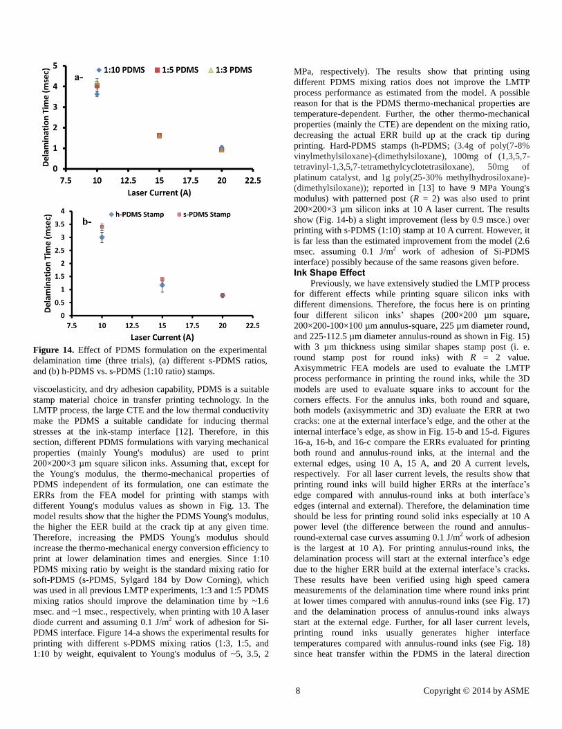
8 Copyright © 2014 by ASME
Figure 14. Effect of PDMS formulation on the experimental
delamination time (three trials), (a) different s-PDMS ratios,
and (b) h-PDMS vs. s-PDMS (1:10 ratio) stamps.
viscoelasticity, and dry adhesion capability, PDMS is a suitable
stamp material choice in transfer printing technology. In the
LMTP process, the large CTE and the low thermal conductivity
make the PDMS a suitable candidate for inducing thermal
stresses at the ink-stamp interface [12]. Therefore, in this
section, different PDMS formulations with varying mechanical
properties (mainly Young's modulus) are used to print
200×200×3 µm square silicon inks. Assuming that, except for
the Young's modulus, the thermo-mechanical properties of
PDMS independent of its formulation, one can estimate the
ERRs from the FEA model for printing with stamps with
different Young's modulus values as shown in Fig. 13. The
model results show that the higher the PDMS Young's modulus,
the higher the EER build at the crack tip at any given time.
Therefore, increasing the PMDS Young's modulus should
increase the thermo-mechanical energy conversion efficiency to
print at lower delamination times and energies. Since 1:10
PDMS mixing ratio by weight is the standard mixing ratio for
soft-PDMS (s-PDMS, Sylgard 184 by Dow Corning), which
was used in all previous LMTP experiments, 1:3 and 1:5 PDMS
mixing ratios should improve the delamination time by ~1.6
msec. and ~1 msec., respectively, when printing with 10 A laser
diode current and assuming 0.1 J/m2 work of adhesion for Si-
PDMS interface. Figure 14-a shows the experimental results for
printing with different s-PDMS mixing ratios (1:3, 1:5, and
1:10 by weight, equivalent to Young's modulus of ~5, 3.5, 2
MPa, respectively). The results show that printing using
different PDMS mixing ratios does not improve the LMTP
process performance as estimated from the model. A possible
reason for that is the PDMS thermo-mechanical properties are
temperature-dependent. Further, the other thermo-mechanical
properties (mainly the CTE) are dependent on the mixing ratio,
decreasing the actual ERR build up at the crack tip during
printing. Hard-PDMS stamps (h-PDMS; (3.4g of poly(7-8%
vinylmethylsiloxane)-(dimethylsiloxane), 100mg of (1,3,5,7-
tetravinyl-1,3,5,7-tetramethylcyclotetrasiloxane), 50mg of
platinum catalyst, and 1g poly(25-30% methylhydrosiloxane)-
(dimethylsiloxane)); reported in [13] to have 9 MPa Young's
modulus) with patterned post (R = 2) was also used to print
200×200×3 µm silicon inks at 10 A laser current. The results
show (Fig. 14-b) a slight improvement (less by 0.9 msce.) over
printing with s-PDMS (1:10) stamp at 10 A current. However, it
is far less than the estimated improvement from the model (2.6
msec. assuming 0.1 J/m2 work of adhesion of Si-PDMS
interface) possibly because of the same reasons given before.
Ink Shape Effect Previously, we have extensively studied the LMTP process
for different effects while printing square silicon inks with
different dimensions. Therefore, the focus here is on printing
four different silicon inks’ shapes (200×200 µm square,
200×200-100×100 µm annulus-square, 225 µm diameter round,
and 225-112.5 µm diameter annulus-round as shown in Fig. 15)
with 3 µm thickness using similar shapes stamp post (i. e.
round stamp post for round inks) with R = 2 value. Axisymmetric FEA models are used to evaluate the LMTP
process performance in printing the round inks, while the 3D
models are used to evaluate square inks to account for the
corners effects. For the annulus inks, both round and square,
both models (axisymmetric and 3D) evaluate the ERR at two
cracks: one at the external interface’s edge, and the other at the
internal interface’s edge, as show in Fig. 15-b and 15-d. Figures
16-a, 16-b, and 16-c compare the ERRs evaluated for printing
both round and annulus-round inks, at the internal and the
external edges, using 10 A, 15 A, and 20 A current levels,
respectively. For all laser current levels, the results show that
printing round inks will build higher ERRs at the interface’s
edge compared with annulus-round inks at both interface’s
edges (internal and external). Therefore, the delamination time
should be less for printing round solid inks especially at 10 A
power level (the difference between the round and annulus-
round-external case curves assuming 0.1 J/m2 work of adhesion
is the largest at 10 A). For printing annulus-round inks, the
delamination process will start at the external interface’s edge
due to the higher ERR build at the external interface’s cracks.
These results have been verified using high speed camera
measurements of the delamination time where round inks print
at lower times compared with annulus-round inks (see Fig. 17)
and the delamination process of annulus-round inks always
start at the external edge. Further, for all laser current levels,
printing round inks usually generates higher interface
temperatures compared with annulus-round inks (see Fig. 18)
since heat transfer within the PDMS in the lateral direction
9 Copyright © 2014 by ASME
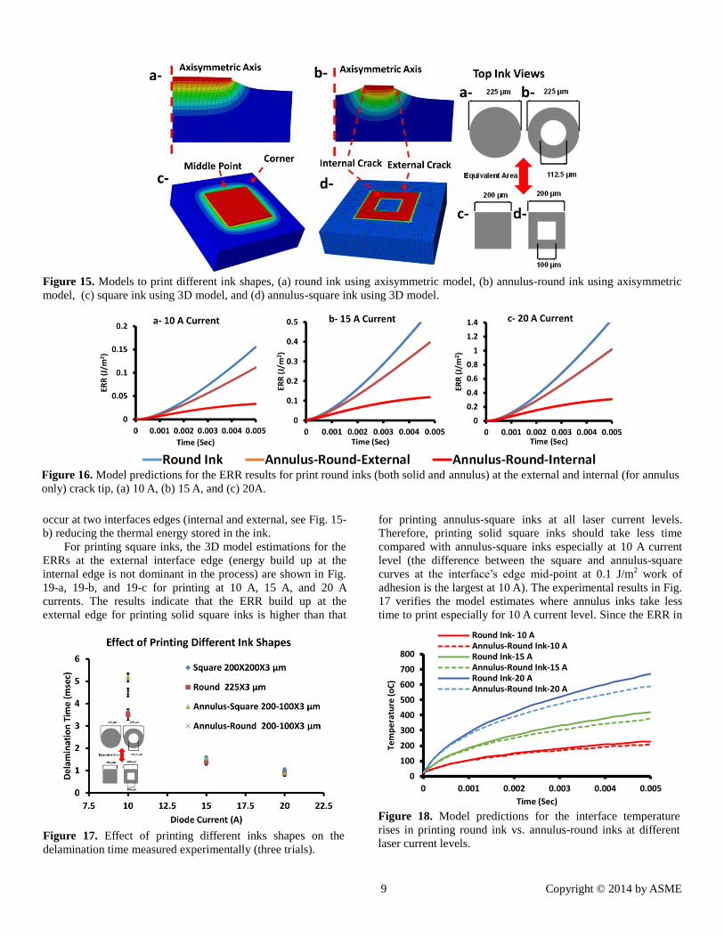
Figure 15. Models to print different ink shapes, (a) round ink using axisymmetric model, (b) annulus-round ink using axisymmetric
model, (c) square ink using 3D model, and (d) annulus-square ink using 3D model.
Figure 16. Model predictions for the ERR results for print round inks (both solid and annulus) at the external and internal (for annulus
only) crack tip, (a) 10 A, (b) 15 A, and (c) 20A.
Figure 17. Effect of printing different inks shapes on the
delamination time measured experimentally (three trials).
.
Figure 18. Model predictions for the interface temperature
rises in printing round ink vs. annulus-round inks at different
laser current levels.
.
0
100
200
300
400
500
600
700
800
0 0.001 0.002 0.003 0.004 0.005
Tem
pe
ratu
re (o
C)
Time (Sec)
Round Ink- 10 AAnnulus-Round Ink-10 ARound Ink-15 AAnnulus-Round Ink-15 ARound Ink-20 AAnnulus-Round Ink-20 A
occur at two interfaces edges (internal and external, see Fig. 15-
b) reducing the thermal energy stored in the ink.
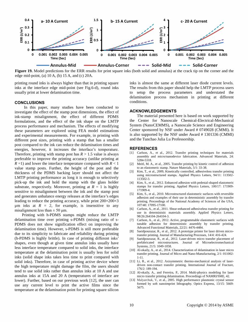
For printing square inks, the 3D model estimations for the
ERRs at the external interface edge (energy build up at the
internal edge is not dominant in the process) are shown in Fig.
19-a, 19-b, and 19-c for printing at 10 A, 15 A, and 20 A
currents. The results indicate that the ERR build up at the
external edge for printing solid square inks is higher than that
for printing annulus-square inks at all laser current levels.
Therefore, printing solid square inks should take less time
compared with annulus-square inks especially at 10 A current
level (the difference between the square and annulus-square
curves at the interface’s edge mid-point at 0.1 J/m2 work of
adhesion is the largest at 10 A). The experimental results in Fig.
17 verifies the model estimates where annulus inks take less
time to print especially for 10 A current level. Since the ERR in
10 Copyright © 2014 by ASME
Figure 19. Model predictions for the ERR results for print square inks (both solid and annulus) at the crack tip on the corner and the
edge mid-point, (a) 10 A, (b) 15 A, and (c) 20A.
printing round inks is always higher than that in printing square
inks at the interface edge mid-point (see Fig.6-d), round inks
usually print at lower delamination time.
CONCLUSIONS
In this paper, many studies have been conducted to
investigate the effect of the stamp post dimensions, the effect of
ink-stamp misalignment, the effect of different PDMS
formulations, and the effect of the ink shape on the LMTP
process performance and mechanism. The effects of modifying
these parameters are explored using FEA model estimations
and experimental measurements. For example, in printing with
different post sizes, printing with a stamp that has a smaller
post compared to the ink can reduce the delamination times and
energies, however, it increases the interface’s temperature.
Therefore, printing with stamp post has R > 1.5 value is always
preferable to improve the printing accuracy (unlike printing at
R =1) and lower the interface temperature compared with R < 1
value stamp posts. Further, the height of the post and the
thickness of the PDMS backing layer should not affect the
LMTP printing performance as long it is enough to selectively
pick-up the ink and hold the stamp with the glass holder
substrate, respectively. Moreover, printing at R = 1 is highly
sensitive to misalignment between the ink and the stamp post
and generates unbalance energy releases at the interface’s edges
leading to reduce the printing accuracy, while print 200×200×3
µm inks at R = 2, for example, is insensitive to any
misalignment less than ± 50 μm.
Printing with h-PDMS stamps might reduce the LMTP
delamination time over printing s-PDMS (mixing ratio of s-
PDMS does not show signification effect on improving the
delamination time). However, s-PDMS is still more preferable
due to its simplicity to fabricate and reliability during printing
(h-PDMS is highly brittle). In case of printing different inks’
shapes, even though at given time annulus inks usually have
less interface temperature compared to solid inks, the interface
temperature at the delamination point is usually less for solid
inks (solid shape inks takes less time to print compared with
solid inks). Therefore, in case of printing active device where
the high temperature might damage the film, the users should
tend to use solid inks rather than annulus inks at 10 A and use
annulus inks at 15A and 20 A (temperatures of interface are
lower). Further, based on our previous work [12], the user can
use any current level to print the active films since the
temperature at the delamination point for printing square silicon
inks is almost the same at different laser diode current levels.
The results from this paper should help the LMTP process users
to setup the process parameters and understated the
delamination process mechanism in printing at different
conditions.
ACKNOWLEDGEMENTS
The material presented here is based on work supported by
the Center for Nanoscale Chemical-Electrical-Mechanical
System (NanoCEMMS), a Nanoscale Science and Engineering
Center sponsored by NSF under Award # 0749028 (CMMI). It
is also supported by the NSF under Award # 1301336 (CMMI)
and the Tunchao Julia Lu Professorship.
REFERENCES [1] Carlson, A., et al., 2012. Transfer printing techniques for materials
assembly and micro/nanodevice fabrication. Advanced Materials, 24:
5284-5318. [2] Meitl, M. A., et al., 2005. Transfer printing by kinetic control of adhesion
to an elastomeric stamp. Nature Materials, 5/1: 33-38.
[3] Kim, T., et al., 2009, Kinetically controlled, adhesiveless transfer printing
using microstructured stamps. Applied Physics Letters, 94/11: 113502-
113502-3.
[4] Kim, S., et al., 2012. Enhanced adhesion with pedestal-shaped elastomeric stamps for transfer printing. Applied Physics Letters, 100/17: 171909-
171909-4.
[5] Kim, S., et al., 2010. Microstructured elastomeric surfaces with reversible adhesion and examples of their use in deterministic assembly by transfer
printing. Proceedings of the National Academy of Sciences of the USA,
107/40: 17095-17100. [6] Carlson, A., et al., 2011. Shear-enhanced adhesiveless transfer printing for
use in deterministic materials assembly. Applied Physics Letters,
98/26:264104-264104-3. [7] Carlson, A., et al., 2012. Active, programmable elastomeric surfaces with
tunable adhesion for deterministic assembly by transfer printing.
Advanced Functional Materials, 22/21: 4476-4484. [8] Saeidpourazar, R., et al., 2012. A prototype printer for laser driven micro-
transfer printing. Journal of Manufacturing Processes, 14/4: 416-424.
[9] Saeidpourazar, R., et al., 2012. Laser-driven micro transfer placement of prefabricated microstructures. Journal of Microelectromechanical
Systems, 21/5: 1049-1058.
[10] Al-okaily, A., et al., 2014. Characterization of delamination in laser micro transfer printing. Journal of Micro and Nano-Manufacturing, 2/1: 011002-
1-11.
[11] Li, R., et al., 2012. Axisymmetric thermo-mechanical analysis of laser-driven non-contact transfer printing. International Journal of Fracture,
176/2: 189-194.
[12] Al-okaily, A., and Ferreira, P., 2014. Multi-physics modeling for laser micro transfer printing delamination. Proceedings of NAMRI/SME, 42.
[13] Malyarchuk, V., et al., 2005. High performance plasmonic crystal sensor
formed by soft nanoimprint lithography. Optics Express, 13/15: 5669-5675.