
GADOLINIUM OXIDE / SILICON THIN FILM ... OXIDE / SILICON THIN FILM HETEROJUNCTION SOLID-STATE...
171
GADOLINIUM OXIDE / SILICON THIN FILM HETEROJUNCTION SOLID- STATE NEUTRON DETECTOR THESIS Christopher M. Young, Major, USA AFIT/GNE/ENP/10M-10 DEPARTMENT OF THE AIR FORCE AIR UNIVERSITY AIR FORCE INSTITUTE OF TECHNOLOGY Wright-Patterson Air Force Base, Ohio APPROVED FOR PUBLIC RELEASE; DISTRIBUTION UNLIMITED
-
Upload
vuongtuong -
Category
Documents
-
view
219 -
download
1
Transcript of GADOLINIUM OXIDE / SILICON THIN FILM ... OXIDE / SILICON THIN FILM HETEROJUNCTION SOLID-STATE...
GADOLINIUM OXIDE / SILICON THIN FILM HETEROJUNCTION SOLID-
STATE NEUTRON DETECTOR
THESIS
Christopher M. Young, Major, USA
AFIT/GNE/ENP/10M-10
DEPARTMENT OF THE AIR FORCE
AIR UNIVERSITY
AIR FORCE INSTITUTE OF TECHNOLOGY
Wright-Patterson Air Force Base, Ohio
APPROVED FOR PUBLIC RELEASE; DISTRIBUTION UNLIMITED

The views expressed in this thesis are those of the author and do not reflect the official
policy or position of the United States Air Force, Department of Defense, or the United
States Government.

AFIT/GNE/ENP/10M-10
GADOLINIUM OXIDE / SILICON THIN FILM HETEROJUNCTION SOLID-STATE
NEUTRON DETECTOR
THESIS
Presented to the Faculty
Department of Engineering Physics
Graduate School of Engineering and Management
Air Force Institute of Technology
Air University
Air Education and Training Command
In Partial Fulfillment of the Requirements for the
Degree of Master of Science in Nuclear Engineering
Christopher M. Young, BS
Major, USA
March 2010
APPROVED FOR PUBLIC RELEASE; DISTRIBUTION UNLIMITED
AFIT/GNE/ENP/10M-10
GADOLINIUM OXIDE / SILICON THIN FILM HETEROJUNCTION SOLID-STATE
NEUTRON DETECTOR
Christopher M. Young, BS
Major, USA
Approved:
iv
AFIT/GNE/ENP/10M-10
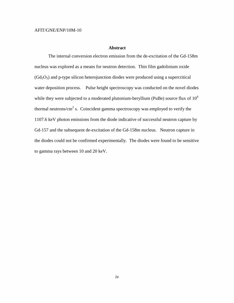
Abstract
The internal conversion electron emission from the de-excitation of the Gd-158m
nucleus was explored as a means for neutron detection. Thin film gadolinium oxide
(Gd2O3) and p-type silicon heterojunction diodes were produced using a supercritical
water deposition process. Pulse height spectroscopy was conducted on the novel diodes
while they were subjected to a moderated plutonium-beryllium (PuBe) source flux of 104
thermal neutrons/cm2 s. Coincident gamma spectroscopy was employed to verify the
1107.6 keV photon emissions from the diode indicative of successful neutron capture by
Gd-157 and the subsequent de-excitation of the Gd-158m nucleus. Neutron capture in
the diodes could not be confirmed experimentally. The diodes were found to be sensitive
to gamma rays between 10 and 20 keV.

v
AFIT/GNE/ENP/10M-10
Dedications
To my family.

vi
Table of Contents Page
Abstract ............................................................................................................................... iv
Dedications .......................................................................................................................... v
Table of Contents……… .................................................................................................... vi
List of Figure……............................................................................................................... ix
List of Tables .................................................................................................................... xiv
List of Abbreviations ......................................................................................................... xv
I. INTRODUCTION ........................................................................................................... 1
1.1 Theory of Special Nuclear Material Detection ......................................................... 2
1.2 Problem Statement .................................................................................................... 7
1.3 Document Organization ............................................................................................ 7
II. BACKGROUND ............................................................................................................ 8
2.1 Properties of Detector Materials .............................................................................. 8
2.2 Detector Technologies............................................................................................ 13
2.3 Gadolinium ............................................................................................................. 14
III. EXPERIMENTAL APPROACH................................................................................ 17
3.1 Introduction ............................................................................................................ 17
3.2 Supercritical Gadolinium Oxide Deposition .......................................................... 17
3.3 Diode Fabrication ................................................................................................... 22
3.4 Initial Device Characterization............................................................................... 24
3.5 Feasibility of Neutron Detection ............................................................................ 26
3.6 Diode Signal and Neutron Flux .............................................................................. 30
3.7 Experimental Concept ............................................................................................ 33
3.7.1 Goal ................................................................................................................. 33
3.7.2 Coincidence Measurements ............................................................................. 33
3.7.3 Neutron Source ................................................................................................ 35
IV. EXPERIMENT, RESULTS, AND ANALYSIS ........................................................ 37
4.1 Experimental Design & Apparatus ........................................................................ 37
vii
4.1.1 Construction of the Neutron Howitzer ............................................................. 37
4.1.2 Coincident Gamma-Ray Instrumentation Scheme ........................................... 43
4.1.3 Establishing the laboratory ............................................................................... 46
4.2 Calibration of the Coincident Gamma-Ray Instrumentation .................................. 48
4.3 Neutron Detection Experiment using Neutron Howitzer ........................................ 54
4.4 Neutron Flux Measurement and Calibration ........................................................... 63
4.5 Neutron Detection Experiment using the Graphite Pile .......................................... 73
4.6 Sr-90 Experiment .................................................................................................... 87
4.7 Cesium-137 Experiment .......................................................................................... 95
V. CONCLUSIONS .......................................................................................................... 99
5.1 Conclusions ............................................................................................................. 99
5.2 Recommendations for future work ........................................................................ 100
5.2.1 Investigate the photon sensitivity. .................................................................. 100
5.2.2 Calibrate the diode spectrum. ......................................................................... 100
5.2.3 Diode modeling. ............................................................................................. 101
APPENDICES ................................................................................................................ 102
Appendix A: Diode Active Volume and Coincident Counting Time ......................... 103
Appendix B: SNM Spontaneous Neutron Emission Rate Calculation ....................... 105
Appendix C: PuBe Source Neutron Emission Rate Calculation [30] ......................... 106
Appendix D: MCNP Code for Neutron Howitzer Design .......................................... 108
D.1 Aluminum Howitzer ......................................................................................... 108
D.2 PVC Howitzer ................................................................................................... 111
Appendix E: MCNP Code for Graphite Pile Differential Neutron Flux ..................... 114
E.1 Differential Neutron Flux at the diode .............................................................. 114
E.2 Differential Neutron Flux at the diode with a Cd absorber ............................... 117
Appendix F: Source and Detector Data Sheets ........................................................... 120
F.1 PuBe Source. ..................................................................................................... 120
F.2 Co-60 Source ..................................................................................................... 121
F.3 LaBr(Ce) Detector Data Sheets ......................................................................... 122
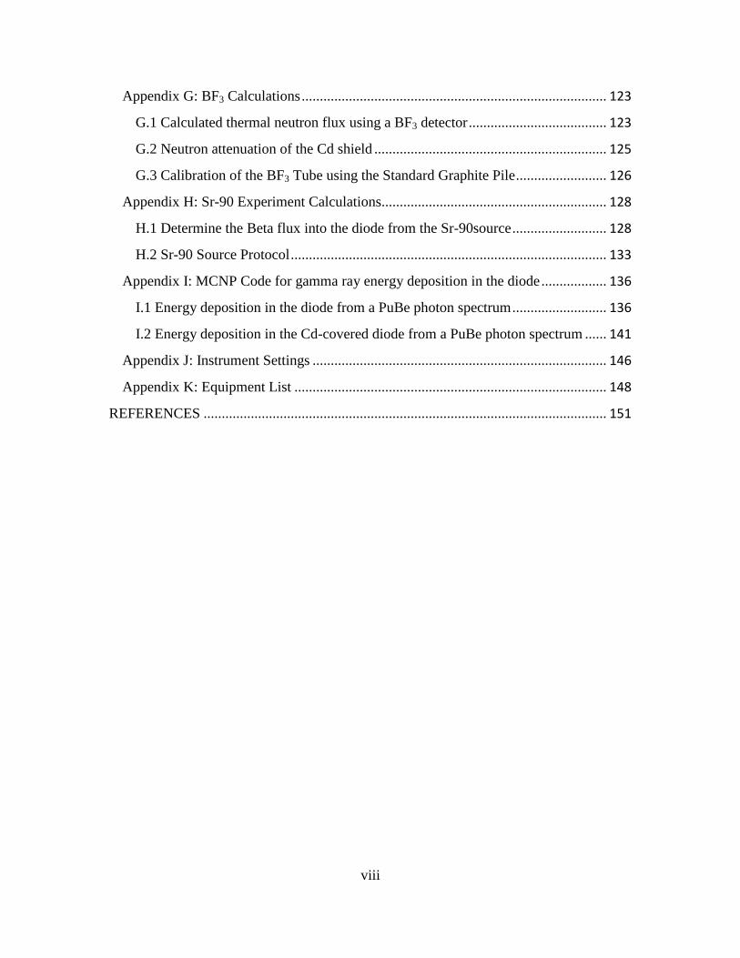
viii
Appendix G: BF3 Calculations .................................................................................... 123
G.1 Calculated thermal neutron flux using a BF3 detector ...................................... 123
G.2 Neutron attenuation of the Cd shield ................................................................ 125
G.3 Calibration of the BF3 Tube using the Standard Graphite Pile ......................... 126
Appendix H: Sr-90 Experiment Calculations.............................................................. 128
H.1 Determine the Beta flux into the diode from the Sr-90source .......................... 128
H.2 Sr-90 Source Protocol ....................................................................................... 133
Appendix I: MCNP Code for gamma ray energy deposition in the diode .................. 136
I.1 Energy deposition in the diode from a PuBe photon spectrum .......................... 136
I.2 Energy deposition in the Cd-covered diode from a PuBe photon spectrum ...... 141
Appendix J: Instrument Settings ................................................................................. 146
Appendix K: Equipment List ...................................................................................... 148
REFERENCES ............................................................................................................... 151
ix
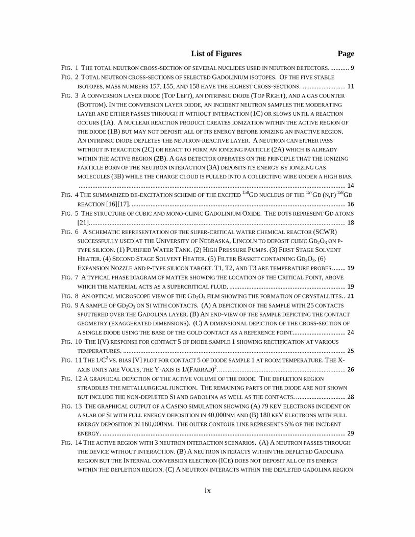
List of Figures Page
FIG. 1 THE TOTAL NEUTRON CROSS-SECTION OF SEVERAL NUCLIDES USED IN NEUTRON DETECTORS. ........... 9 FIG. 2 TOTAL NEUTRON CROSS-SECTIONS OF SELECTED GADOLINIUM ISOTOPES. OF THE FIVE STABLE
ISOTOPES, MASS NUMBERS 157, 155, AND 158 HAVE THE HIGHEST CROSS-SECTIONS. .......................... 11 FIG. 3 A CONVERSION LAYER DIODE (TOP LEFT), AN INTRINSIC DIODE (TOP RIGHT), AND A GAS COUNTER
(BOTTOM). IN THE CONVERSION LAYER DIODE, AN INCIDENT NEUTRON SAMPLES THE MODERATING
LAYER AND EITHER PASSES THROUGH IT WITHOUT INTERACTION (1C) OR SLOWS UNTIL A REACTION
OCCURS (1A). A NUCLEAR REACTION PRODUCT CREATES IONIZATION WITHIN THE ACTIVE REGION OF
THE DIODE (1B) BUT MAY NOT DEPOSIT ALL OF ITS ENERGY BEFORE IONIZING AN INACTIVE REGION.
AN INTRINSIC DIODE DEPLETES THE NEUTRON-REACTIVE LAYER. A NEUTRON CAN EITHER PASS
WITHOUT INTERACTION (2C) OR REACT TO FORM AN IONIZING PARTICLE (2A) WHICH IS ALREADY
WITHIN THE ACTIVE REGION (2B). A GAS DETECTOR OPERATES ON THE PRINCIPLE THAT THE IONIZING
PARTICLE BORN OF THE NEUTRON INTERACTION (3A) DEPOSITS ITS ENERGY BY IONIZING GAS
MOLECULES (3B) WHILE THE CHARGE CLOUD IS PULLED INTO A COLLECTING WIRE UNDER A HIGH BIAS.
............................................................................................................................................................ 14 FIG. 4 THE SUMMARIZED DE-EXCITATION SCHEME OF THE EXCITED
158GD NUCLEUS OF THE
157GD (N,Γ)
158GD
REACTION [16][17]. ............................................................................................................................. 16 FIG. 5 THE STRUCTURE OF CUBIC AND MONO-CLINIC GADOLINIUM OXIDE. THE DOTS REPRESENT GD ATOMS
[21]. ..................................................................................................................................................... 18 FIG. 6 A SCHEMATIC REPRESENTATION OF THE SUPER-CRITICAL WATER CHEMICAL REACTOR (SCWR)
SUCCESSFULLY USED AT THE UNIVERSITY OF NEBRASKA, LINCOLN TO DEPOSIT CUBIC GD2O3 ON P-
TYPE SILICON. (1) PURIFIED WATER TANK. (2) HIGH PRESSURE PUMPS. (3) FIRST STAGE SOLVENT
HEATER. (4) SECOND STAGE SOLVENT HEATER. (5) FILTER BASKET CONTAINING GD2O3. (6)
EXPANSION NOZZLE AND P-TYPE SILICON TARGET. T1, T2, AND T3 ARE TEMPERATURE PROBES. ....... 19 FIG. 7 A TYPICAL PHASE DIAGRAM OF MATTER SHOWING THE LOCATION OF THE CRITICAL POINT, ABOVE
WHICH THE MATERIAL ACTS AS A SUPERCRITICAL FLUID. .................................................................... 19
FIG. 8 AN OPTICAL MICROSCOPE VIEW OF THE GD2O3 FILM SHOWING THE FORMATION OF CRYSTALLITES. . 21 FIG. 9 A SAMPLE OF GD2O3 ON SI WITH CONTACTS. (A) A DEPICTION OF THE SAMPLE WITH 25 CONTACTS
SPUTTERED OVER THE GADOLINA LAYER. (B) AN END-VIEW OF THE SAMPLE DEPICTING THE CONTACT
GEOMETRY (EXAGGERATED DIMENSIONS). (C) A DIMENSIONAL DEPICTION OF THE CROSS-SECTION OF
A SINGLE DIODE USING THE BASE OF THE GOLD CONTACT AS A REFERENCE POINT. .............................. 24 FIG. 10 THE I(V) RESPONSE FOR CONTACT 5 OF DIODE SAMPLE 1 SHOWING RECTIFICATION AT VARIOUS
TEMPERATURES. .................................................................................................................................. 25 FIG. 11 THE 1/C
2 VS. BIAS [V] PLOT FOR CONTACT 5 OF DIODE SAMPLE 1 AT ROOM TEMPERATURE. THE X-
AXIS UNITS ARE VOLTS, THE Y-AXIS IS 1/(FARRAD)2. .......................................................................... 26
FIG. 12 A GRAPHICAL DEPICTION OF THE ACTIVE VOLUME OF THE DIODE. THE DEPLETION REGION
STRADDLES THE METALLURGICAL JUNCTION. THE REMAINING PARTS OF THE DIODE ARE NOT SHOWN
BUT INCLUDE THE NON-DEPLETED SI AND GADOLINA AS WELL AS THE CONTACTS. ............................. 28 FIG. 13 THE GRAPHICAL OUTPUT OF A CASINO SIMULATION SHOWING (A) 79 KEV ELECTRONS INCIDENT ON
A SLAB OF SI WITH FULL ENERGY DEPOSITION IN 40,000NM AND (B) 180 KEV ELECTRONS WITH FULL
ENERGY DEPOSITION IN 160,000NM. THE OUTER CONTOUR LINE REPRESENTS 5% OF THE INCIDENT
ENERGY. .............................................................................................................................................. 29 FIG. 14 THE ACTIVE REGION WITH 3 NEUTRON INTERACTION SCENARIOS. (A) A NEUTRON PASSES THROUGH
THE DEVICE WITHOUT INTERACTION. (B) A NEUTRON INTERACTS WITHIN THE DEPLETED GADOLINA
REGION BUT THE INTERNAL CONVERSION ELECTRON (ICE) DOES NOT DEPOSIT ALL OF ITS ENERGY
WITHIN THE DEPLETION REGION. (C) A NEUTRON INTERACTS WITHIN THE DEPLETED GADOLINA REGION

x
AND THE INTERNAL CONVERSION ELECTRON (ICE) DEPOSITS ALL OF ITS ENERGY WITHIN THE
DEPLETION REGION. ............................................................................................................................. 30 FIG. 15 A PLOT OF THE EXPECTED ELECTRICAL SIGNAL FROM THE ACTIVE VOLUME (LEFT-SIDE) AND A PRE-
AMPLIFIER OUTPUT VOLTAGE (RIGHT-SIDE) AS FUNCTION OF THERMAL NEUTRON FLUX FOR THE 79
KEV ICE. THE CONVERSION OF CURRENT TO VOLTAGE USES THE FACTOR OF 0.64 µV PER ELECTRON
HOLE PAIR WHICH IS TYPICAL OF THE AMPTEK A250CF PREAMPLIFER. .............................................. 32 FIG. 16 A SCHEMATIC AND PICTORIAL DEPICTION OF A COINCIDENT DETECTOR ARRANGEMENT TO RECORD A
NEUTRON CAPTURE PULSE IN COINCIDENCE WITH A GAMMA EMISSION BORN OF THE SAME REACTION. 34 FIG. 17 A SIMPLIFIED SCHEME OF USING TANDEM “NEUTRON HOWITZERS” POWERED BY PUBE SOURCES TO
IRRADIATE A SAMPLE DIODE WITH THERMALIZED NEUTRONS. ............................................................. 36 FIG. 18 A SIMPLIFIED DIMENSIONAL DRAWING OF THE PLANNED NEUTRON HOWITZER THAT WAS TO BE
CONSTRUCTED OF ALUMINUM TUBING WITHIN A 55 GALLON DRUM ABLE TO ACCOMMODATE LARGER
EXPERIMENTS. THIS HOWITZER WAS NOT BUILT. ................................................................................. 37 FIG. 19 THE DIMENSIONS OF THE NEUTRON HOWITZER AS BUILT WITH PVC PIPE. THE CROSS-SECTION OF
THE HOWITZER AS SEE FROM THE SIDE IS SHOWN IN „A.‟ THE DETAILS OF THE FIXED CENTRAL TUBE
AND MOVEABLE INNER TUBE ARE SHOWN IN „B.‟ „C‟ SHOWS THE DETAIL OF THE INNER TUBE AS
OBSERVED WITH THE SAME ASPECT OF „A‟,‟B‟, AND „C‟. „D‟ SHOWS THE INNER TUBE WITH THE
SOURCE OPENING ROTATED 90 DEGREES TOWARD THE OBSERVER. DETAILS „B‟,‟C‟, AND „D‟ ARE
DRAWN TO SCALE. „A‟ IS NOT TO SCALE AND REPRESENTS THE DIMENSIONS OF A 55 GALLON DRUM. . 38 FIG. 20 THE NEUTRON HOWITZER PVC COMPONENTS. „A‟ THE MOVING AND FIXED TUBES WITH PIECES OF
WOOD INDICATING THE THICKNESS AND LOCATION OF THE PLUGS INSIDE THE INNER TUBE. „B‟ A
DETAIL OF THE SOURCE HOLDER AS WELL AS THE BOTTOM OF THE CENTER TUBE WHICH IS A CLEAN-
OUT THAT IS TO BE ANCHORED INSIDE THE DRUM. ............................................................................... 39 FIG. 21 THE FINAL ASSEMBLY OF THE NEUTRON HOWITZER. „A‟ CAMP STOVES WERE USED TO MELT THE
PARAFFIN WAX OUTDOORS. „B‟ THE PVC TUBES ANCHORED INTO THE DRUM AND A FEW INCHES OF
WAX. „C‟ THE WAX HAD TO BE MELTED A FEW OUNCES AT A TIME. MAINTAINING LIQUID WAX IN THE
MELT WAS IMPORTANT FOR HEAT TRANSFER. „D‟ UNEVEN COOLING OF THE WAX PRODUCED
CONTRACTION POCKETS WHICH WERE FILLED WITH WAX IN SUBSEQUENT POURS................................ 40 FIG. 22 THE NEUTRON SPECTRUM FROM THE PLUTONIUM-BERYLLIUM SOURCE USED FOR MCNP5
MODELING. .......................................................................................................................................... 41 FIG. 23 THE DIFFERENTIAL NEUTRON FLUX AT THE BEAM TUBE OUTPUT OF THE PUBE SOURCE FOR THE
TWO NEUTRON HOWITZER DESIGNS...................................................................................................... 42 FIG. 24 THE INITIAL INSTRUMENT SCHEME FOR COINCIDENT MEASUREMENT. THE UNEQUAL RESPONSE OF
THE PMTS PROMPTED EXPERIMENTING WITH SEPARATE POWER SUPPLIES BUT THIS ARRANGEMENT
WAS EVENTUALLY CHANGED TO EMPLOY SEPARATE SCAS. THE LINEAR AMPLIFIER PROVIDES THE
POWER FOR THE PRE-AMPLIFIER. .......................................................................................................... 44 FIG. 25 THE FINAL INSTRUMENT SCHEME FOR COINCIDENT MEASUREMENT. THE USE OF SEPARATE
AMPLIFIERS AND SCAS ALLOWED EACH SCINTILLATOR CIRCUIT TO BE CALIBRATED TO SEND A GATE
PULSE UPON THE DETECTION OF AN 1107.6 KEV EVENT....................................................................... 45 FIG. 26 BENCH TESTING THE COINCIDENT DETECTION SCHEME. „A‟ THE INSTRUMENTATION SETUP ON THE
BENCH. „B‟ A DETAIL OF THE LABR(CE) SCINTILLATOR AND INTEGRATED PMTS. .............................. 46 FIG. 27 A SCHEMATIC OF THE LABORATORY DEPICTING THE RESULTS OF THE GAMMA RADIATION SURVEY
BEFORE AND AFTER LOADING THE HOWITZER. „A‟ INDICATES BACKGROUND GAMMA LEVELS PRIOR TO
LOADING THE HOWITZER, „B‟ INDICATES THE LEVELS AFTER LOADING WITH THE SOURCE IN THE BEAM
POSITION. LOCATION 8 IS A LEAD BOX HOUSING A SMALL CO-60 TEST SOURCE. ................................. 47
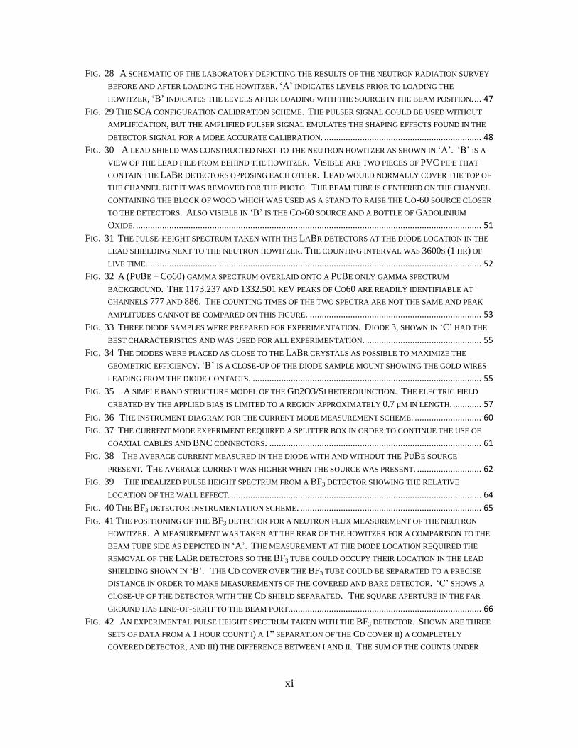
xi
FIG. 28 A SCHEMATIC OF THE LABORATORY DEPICTING THE RESULTS OF THE NEUTRON RADIATION SURVEY
BEFORE AND AFTER LOADING THE HOWITZER. „A‟ INDICATES LEVELS PRIOR TO LOADING THE
HOWITZER, „B‟ INDICATES THE LEVELS AFTER LOADING WITH THE SOURCE IN THE BEAM POSITION. ... 47 FIG. 29 THE SCA CONFIGURATION CALIBRATION SCHEME. THE PULSER SIGNAL COULD BE USED WITHOUT
AMPLIFICATION, BUT THE AMPLIFIED PULSER SIGNAL EMULATES THE SHAPING EFFECTS FOUND IN THE
DETECTOR SIGNAL FOR A MORE ACCURATE CALIBRATION. .................................................................. 48 FIG. 30 A LEAD SHIELD WAS CONSTRUCTED NEXT TO THE NEUTRON HOWITZER AS SHOWN IN „A‟. „B‟ IS A
VIEW OF THE LEAD PILE FROM BEHIND THE HOWITZER. VISIBLE ARE TWO PIECES OF PVC PIPE THAT
CONTAIN THE LABR DETECTORS OPPOSING EACH OTHER. LEAD WOULD NORMALLY COVER THE TOP OF
THE CHANNEL BUT IT WAS REMOVED FOR THE PHOTO. THE BEAM TUBE IS CENTERED ON THE CHANNEL
CONTAINING THE BLOCK OF WOOD WHICH WAS USED AS A STAND TO RAISE THE CO-60 SOURCE CLOSER
TO THE DETECTORS. ALSO VISIBLE IN „B‟ IS THE CO-60 SOURCE AND A BOTTLE OF GADOLINIUM
OXIDE. ................................................................................................................................................. 51 FIG. 31 THE PULSE-HEIGHT SPECTRUM TAKEN WITH THE LABR DETECTORS AT THE DIODE LOCATION IN THE
LEAD SHIELDING NEXT TO THE NEUTRON HOWITZER. THE COUNTING INTERVAL WAS 3600S (1 HR) OF
LIVE TIME............................................................................................................................................. 52 FIG. 32 A (PUBE + CO60) GAMMA SPECTRUM OVERLAID ONTO A PUBE ONLY GAMMA SPECTRUM
BACKGROUND. THE 1173.237 AND 1332.501 KEV PEAKS OF CO60 ARE READILY IDENTIFIABLE AT
CHANNELS 777 AND 886. THE COUNTING TIMES OF THE TWO SPECTRA ARE NOT THE SAME AND PEAK
AMPLITUDES CANNOT BE COMPARED ON THIS FIGURE. ........................................................................ 53 FIG. 33 THREE DIODE SAMPLES WERE PREPARED FOR EXPERIMENTATION. DIODE 3, SHOWN IN „C‟ HAD THE
BEST CHARACTERISTICS AND WAS USED FOR ALL EXPERIMENTATION. ................................................ 55 FIG. 34 THE DIODES WERE PLACED AS CLOSE TO THE LABR CRYSTALS AS POSSIBLE TO MAXIMIZE THE
GEOMETRIC EFFICIENCY. „B‟ IS A CLOSE-UP OF THE DIODE SAMPLE MOUNT SHOWING THE GOLD WIRES
LEADING FROM THE DIODE CONTACTS. ................................................................................................ 55 FIG. 35 A SIMPLE BAND STRUCTURE MODEL OF THE GD2O3/SI HETEROJUNCTION. THE ELECTRIC FIELD
CREATED BY THE APPLIED BIAS IS LIMITED TO A REGION APPROXIMATELY 0.7 µM IN LENGTH. ............ 57
FIG. 36 THE INSTRUMENT DIAGRAM FOR THE CURRENT MODE MEASUREMENT SCHEME. ............................ 60 FIG. 37 THE CURRENT MODE EXPERIMENT REQUIRED A SPLITTER BOX IN ORDER TO CONTINUE THE USE OF
COAXIAL CABLES AND BNC CONNECTORS. ......................................................................................... 61 FIG. 38 THE AVERAGE CURRENT MEASURED IN THE DIODE WITH AND WITHOUT THE PUBE SOURCE
PRESENT. THE AVERAGE CURRENT WAS HIGHER WHEN THE SOURCE WAS PRESENT. ........................... 62 FIG. 39 THE IDEALIZED PULSE HEIGHT SPECTRUM FROM A BF3 DETECTOR SHOWING THE RELATIVE
LOCATION OF THE WALL EFFECT. ......................................................................................................... 64
FIG. 40 THE BF3 DETECTOR INSTRUMENTATION SCHEME. ............................................................................ 65 FIG. 41 THE POSITIONING OF THE BF3 DETECTOR FOR A NEUTRON FLUX MEASUREMENT OF THE NEUTRON
HOWITZER. A MEASUREMENT WAS TAKEN AT THE REAR OF THE HOWITZER FOR A COMPARISON TO THE
BEAM TUBE SIDE AS DEPICTED IN „A‟. THE MEASUREMENT AT THE DIODE LOCATION REQUIRED THE
REMOVAL OF THE LABR DETECTORS SO THE BF3 TUBE COULD OCCUPY THEIR LOCATION IN THE LEAD
SHIELDING SHOWN IN „B‟. THE CD COVER OVER THE BF3 TUBE COULD BE SEPARATED TO A PRECISE
DISTANCE IN ORDER TO MAKE MEASUREMENTS OF THE COVERED AND BARE DETECTOR. „C‟ SHOWS A
CLOSE-UP OF THE DETECTOR WITH THE CD SHIELD SEPARATED. THE SQUARE APERTURE IN THE FAR
GROUND HAS LINE-OF-SIGHT TO THE BEAM PORT. ................................................................................ 66 FIG. 42 AN EXPERIMENTAL PULSE HEIGHT SPECTRUM TAKEN WITH THE BF3 DETECTOR. SHOWN ARE THREE
SETS OF DATA FROM A 1 HOUR COUNT I) A 1” SEPARATION OF THE CD COVER II) A COMPLETELY
COVERED DETECTOR, AND III) THE DIFFERENCE BETWEEN I AND II. THE SUM OF THE COUNTS UNDER
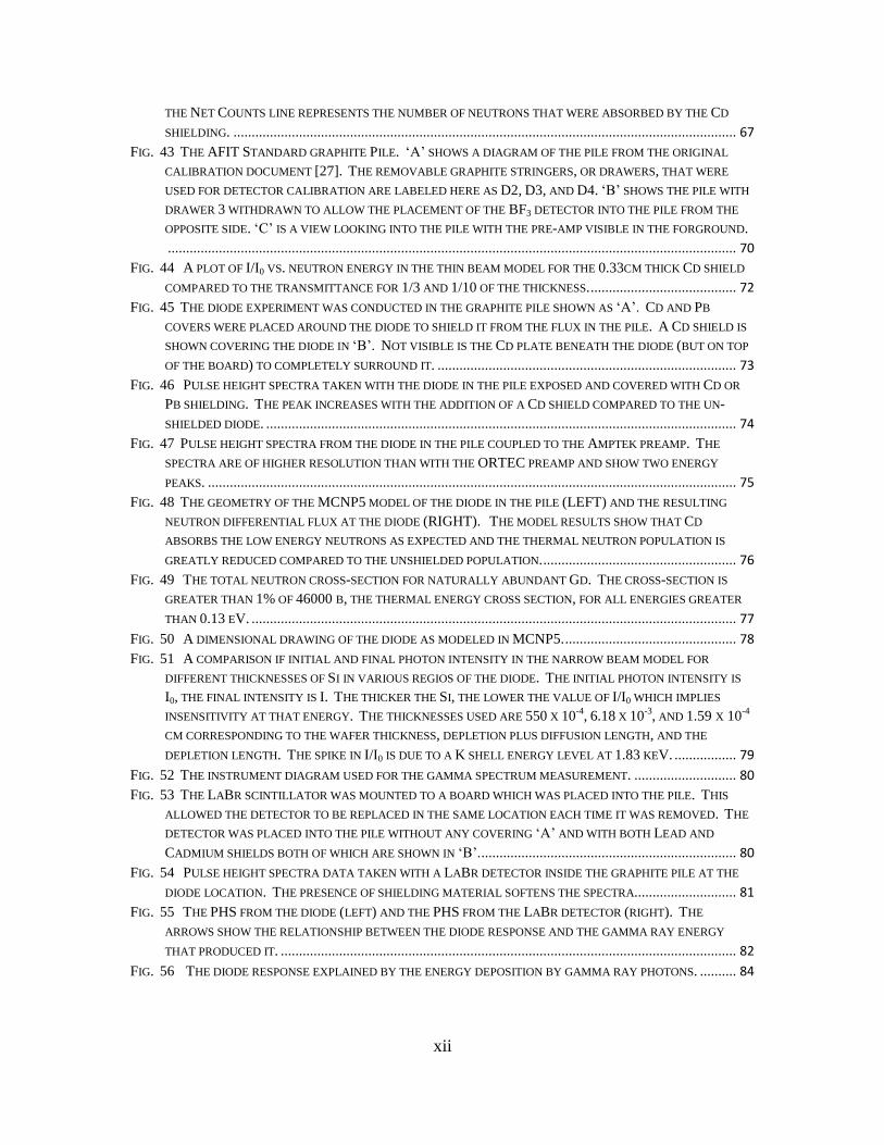
xii
THE NET COUNTS LINE REPRESENTS THE NUMBER OF NEUTRONS THAT WERE ABSORBED BY THE CD
SHIELDING. .......................................................................................................................................... 67 FIG. 43 THE AFIT STANDARD GRAPHITE PILE. „A‟ SHOWS A DIAGRAM OF THE PILE FROM THE ORIGINAL
CALIBRATION DOCUMENT [27]. THE REMOVABLE GRAPHITE STRINGERS, OR DRAWERS, THAT WERE
USED FOR DETECTOR CALIBRATION ARE LABELED HERE AS D2, D3, AND D4. „B‟ SHOWS THE PILE WITH
DRAWER 3 WITHDRAWN TO ALLOW THE PLACEMENT OF THE BF3 DETECTOR INTO THE PILE FROM THE
OPPOSITE SIDE. „C‟ IS A VIEW LOOKING INTO THE PILE WITH THE PRE-AMP VISIBLE IN THE FORGROUND.
............................................................................................................................................................ 70 FIG. 44 A PLOT OF I/I0 VS. NEUTRON ENERGY IN THE THIN BEAM MODEL FOR THE 0.33CM THICK CD SHIELD
COMPARED TO THE TRANSMITTANCE FOR 1/3 AND 1/10 OF THE THICKNESS. ........................................ 72 FIG. 45 THE DIODE EXPERIMENT WAS CONDUCTED IN THE GRAPHITE PILE SHOWN AS „A‟. CD AND PB
COVERS WERE PLACED AROUND THE DIODE TO SHIELD IT FROM THE FLUX IN THE PILE. A CD SHIELD IS
SHOWN COVERING THE DIODE IN „B‟. NOT VISIBLE IS THE CD PLATE BENEATH THE DIODE (BUT ON TOP
OF THE BOARD) TO COMPLETELY SURROUND IT. .................................................................................. 73 FIG. 46 PULSE HEIGHT SPECTRA TAKEN WITH THE DIODE IN THE PILE EXPOSED AND COVERED WITH CD OR
PB SHIELDING. THE PEAK INCREASES WITH THE ADDITION OF A CD SHIELD COMPARED TO THE UN-
SHIELDED DIODE. ................................................................................................................................. 74 FIG. 47 PULSE HEIGHT SPECTRA FROM THE DIODE IN THE PILE COUPLED TO THE AMPTEK PREAMP. THE
SPECTRA ARE OF HIGHER RESOLUTION THAN WITH THE ORTEC PREAMP AND SHOW TWO ENERGY
PEAKS. ................................................................................................................................................. 75 FIG. 48 THE GEOMETRY OF THE MCNP5 MODEL OF THE DIODE IN THE PILE (LEFT) AND THE RESULTING
NEUTRON DIFFERENTIAL FLUX AT THE DIODE (RIGHT). THE MODEL RESULTS SHOW THAT CD
ABSORBS THE LOW ENERGY NEUTRONS AS EXPECTED AND THE THERMAL NEUTRON POPULATION IS
GREATLY REDUCED COMPARED TO THE UNSHIELDED POPULATION. ..................................................... 76 FIG. 49 THE TOTAL NEUTRON CROSS-SECTION FOR NATURALLY ABUNDANT GD. THE CROSS-SECTION IS
GREATER THAN 1% OF 46000 B, THE THERMAL ENERGY CROSS SECTION, FOR ALL ENERGIES GREATER
THAN 0.13 EV. ..................................................................................................................................... 77
FIG. 50 A DIMENSIONAL DRAWING OF THE DIODE AS MODELED IN MCNP5. ............................................... 78 FIG. 51 A COMPARISON IF INITIAL AND FINAL PHOTON INTENSITY IN THE NARROW BEAM MODEL FOR
DIFFERENT THICKNESSES OF SI IN VARIOUS REGIOS OF THE DIODE. THE INITIAL PHOTON INTENSITY IS
I0, THE FINAL INTENSITY IS I. THE THICKER THE SI, THE LOWER THE VALUE OF I/I0 WHICH IMPLIES
INSENSITIVITY AT THAT ENERGY. THE THICKNESSES USED ARE 550 X 10-4
, 6.18 X 10⁻³
, AND 1.59 X 10⁻⁴
CM CORRESPONDING TO THE WAFER THICKNESS, DEPLETION PLUS DIFFUSION LENGTH, AND THE
DEPLETION LENGTH. THE SPIKE IN I/I0 IS DUE TO A K SHELL ENERGY LEVEL AT 1.83 KEV. ................. 79
FIG. 52 THE INSTRUMENT DIAGRAM USED FOR THE GAMMA SPECTRUM MEASUREMENT. ............................ 80 FIG. 53 THE LABR SCINTILLATOR WAS MOUNTED TO A BOARD WHICH WAS PLACED INTO THE PILE. THIS
ALLOWED THE DETECTOR TO BE REPLACED IN THE SAME LOCATION EACH TIME IT WAS REMOVED. THE
DETECTOR WAS PLACED INTO THE PILE WITHOUT ANY COVERING „A‟ AND WITH BOTH LEAD AND
CADMIUM SHIELDS BOTH OF WHICH ARE SHOWN IN „B‟. ...................................................................... 80 FIG. 54 PULSE HEIGHT SPECTRA DATA TAKEN WITH A LABR DETECTOR INSIDE THE GRAPHITE PILE AT THE
DIODE LOCATION. THE PRESENCE OF SHIELDING MATERIAL SOFTENS THE SPECTRA............................ 81 FIG. 55 THE PHS FROM THE DIODE (LEFT) AND THE PHS FROM THE LABR DETECTOR (RIGHT). THE
ARROWS SHOW THE RELATIONSHIP BETWEEN THE DIODE RESPONSE AND THE GAMMA RAY ENERGY
THAT PRODUCED IT. ............................................................................................................................. 82
FIG. 56 THE DIODE RESPONSE EXPLAINED BY THE ENERGY DEPOSITION BY GAMMA RAY PHOTONS. .......... 84

xiii
FIG. 57 THE PHOTON ENERGY SPECTRUM OF THE PUBE SOURCE USED FOR MCNP SIMULATION. THE
SPECTRUM WAS DEVELOPED FROM PUBLISHED DATA TAKEN WITH A HIGH-PURITY GERMANIUM
DETECTOR [26]. ................................................................................................................................... 85 FIG. 58 THE DEPOSITION OF ENERGY IN THE DIODE FROM A PUBE PHOTON SPECTRUM AS DEPOSITED IN SI
OVER AN ELECTRON DIFFUSION LENGTH FROM THE METALLURGICAL JUNCTION. THE MODEL DOES NOT
AGREE WITH THE HYPOTHESIS THAT MORE ENERGY IS DEPOSITED IN THE DEVICE WHEN A CD COVER
INCREASES THE LOW-ENERGY PHOTON POPULATION. .......................................................................... 86
FIG. 59 THE DECAY SCHEMES FOR SR-90 AND Y-90.................................................................................... 88
FIG. 60 THE OVERLAPPING BETA-PARTICLE ENERGY DISTRIBUTIONS OF SR-90 AND Y-90. ......................... 89 FIG. 61 THE SR-90 SOURCE WAS ORIGINALLY PRODUCED AS A MEDICAL APPLICATOR SHOWN IN „A‟. THE
SOURCE, PICTURED IN „B‟ HAS A PLASTIC SHIELD THAT SLIDES UP AND DOWN THE SHAFT WHICH IS
DESIGNED TO SHIELD THE OPERATOR FROM RADIATION. THE SOURCE IS SITTING HEAD-DOWN AND IS
COVERED BY A THICK ALUMINUM SHIELD FOR STORAGE WHICH IS REMOVED FOR USE. THE SR-90 IS
ENCLOSED IN A STAINLESS STEEL AND ALUMINUM ELEMENT ON THE END OF THE APPLICATOR ROD. .. 90
FIG. 62 THE ENERGY DISTRIBUTION OF THE BETA PARTICLES EMITTED FROM THE SOURCE. ........................ 92 FIG. 63 A DIAGRAM OF THE SR-90 EXPERIMENT. PICTURED INSIDE ALUMINUM SHIELDING „4‟, ARE THE
DIODE AND SIGNAL WIRES „2‟, THE SOURCE „1‟, THE CONCRETE FLOOR „3‟, AND THE SOURCE AND
SAMPLE STAND „5‟. .............................................................................................................................. 93 FIG. 64 THE PULSE HEIGHT SPECTRUM TAKEN WITH THE DIODE EXPOSED TO A BETA SOURCE. THE DIODE
RESPONSE WAS HIGHER CLOSER TO THE SOURCE. ................................................................................ 94
FIG. 65 THE DECAY OF CS-137 TO BA-137. ................................................................................................. 95 FIG. 66 THE CS-137 SOURCE BELONGED TO AFFRAD AND IS USED FOR CALIBRATING INSTRUMENTATION.
THE SOURCE IS STORED INSIDE A CONTAINMENT VESSEL LOCATED AT THE END OF A MOVABLE STAND
SHOWN IN „A‟. THE DIODE WAS PLACED 1.608” AWAY FROM THE EXPOSED SOURCE. THIS DISTANCE
WAS ACHIEVED BY PLACING THE DIODE INSIDE THE LINE-OF-SIGHT PORT OF THE PIG AS SHOWN IN „B‟
AND „C‟. CLOSE PLACEMENT MAXIMIZED THE GAMMA FLUX. ............................................................. 97 FIG. 67 THE PULSE HEIGHT SPECTRUM TAKEN FROM THE DIODE DURING IRRADIATION FROM THE 1.2 CI CS-
137 SOURCE. ........................................................................................................................................ 98
xiv
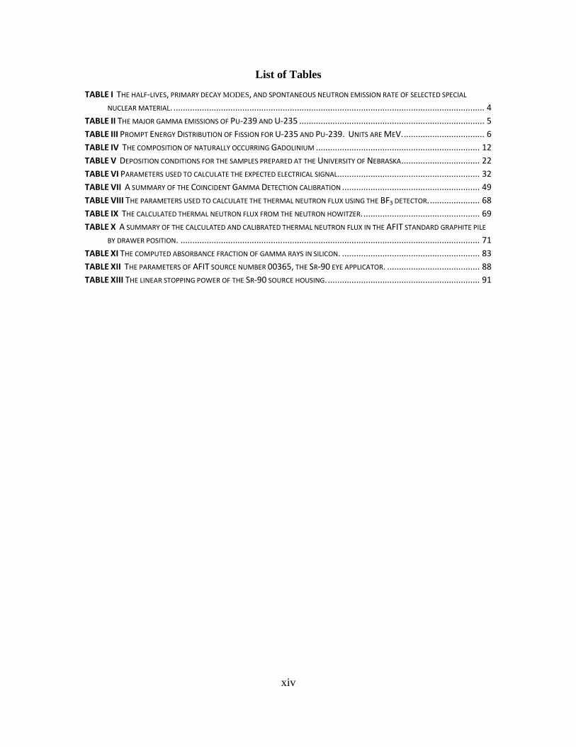
List of Tables
TABLE I THE HALF-LIVES, PRIMARY DECAY MODES, AND SPONTANEOUS NEUTRON EMISSION RATE OF SELECTED SPECIAL
NUCLEAR MATERIAL. ................................................................................................................................... 4
TABLE II THE MAJOR GAMMA EMISSIONS OF PU-239 AND U-235 .............................................................................. 5
TABLE III PROMPT ENERGY DISTRIBUTION OF FISSION FOR U-235 AND PU-239. UNITS ARE MEV. .................................. 6
TABLE IV THE COMPOSITION OF NATURALLY OCCURRING GADOLINIUM ..................................................................... 12
TABLE V DEPOSITION CONDITIONS FOR THE SAMPLES PREPARED AT THE UNIVERSITY OF NEBRASKA ................................. 22
TABLE VI PARAMETERS USED TO CALCULATE THE EXPECTED ELECTRICAL SIGNAL............................................................ 32
TABLE VII A SUMMARY OF THE COINCIDENT GAMMA DETECTION CALIBRATION .......................................................... 49
TABLE VIII THE PARAMETERS USED TO CALCULATE THE THERMAL NEUTRON FLUX USING THE BF3 DETECTOR. ..................... 68
TABLE IX THE CALCULATED THERMAL NEUTRON FLUX FROM THE NEUTRON HOWITZER. ................................................. 69
TABLE X A SUMMARY OF THE CALCULATED AND CALIBRATED THERMAL NEUTRON FLUX IN THE AFIT STANDARD GRAPHITE PILE
BY DRAWER POSITION. .............................................................................................................................. 71
TABLE XI THE COMPUTED ABSORBANCE FRACTION OF GAMMA RAYS IN SILICON. .......................................................... 83
TABLE XII THE PARAMETERS OF AFIT SOURCE NUMBER 00365, THE SR-90 EYE APPLICATOR. ....................................... 88
TABLE XIII THE LINEAR STOPPING POWER OF THE SR-90 SOURCE HOUSING. ................................................................ 91

xv
List of Abbreviations
Abbreviation Description
Alpha Particle
n Neutron
DoD Department of Defense
DTRA Defense Threat Reduction Agency
SNM Special Nuclear Material
eV Electron Volt
MCNP Monte Carlo Neutral Particle
Ci Curie
PuBe Plutonium-Beryllium
β- Beta Particle, an electron
HV High Voltage
LV Low Voltage
PMT Photomultiplier Tube
DLA Delay Line Amplifier
TSCA Timing Single-Channel Analyzer
LLD Lower Level Discriminator
MCB Multi-Channel Buffer
Cd Cadmium
Pb Lead
LaBr Lanthanum Bromide
TSCA Timing Single Channel Analyzer
UPS Uninterruptible Power Supply
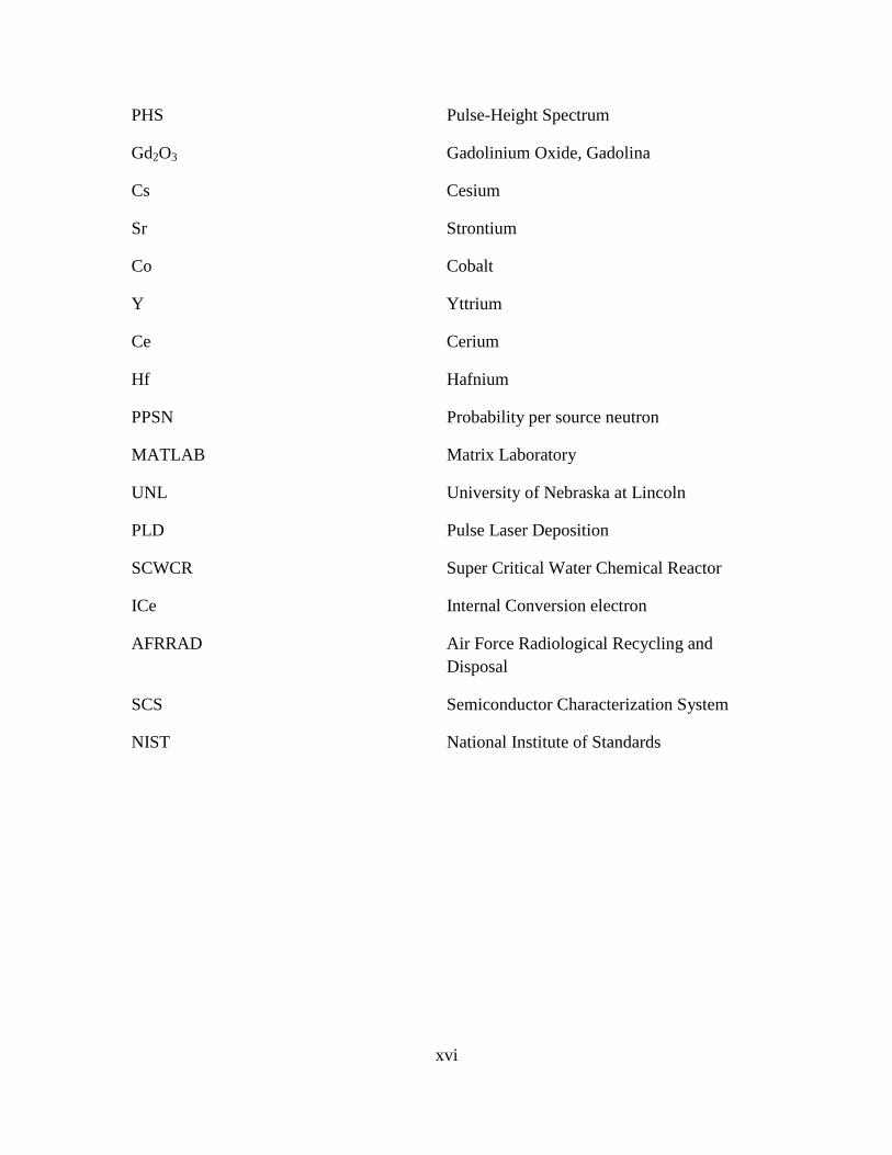
xvi
PHS Pulse-Height Spectrum
Gd2O3 Gadolinium Oxide, Gadolina
Cs Cesium
Sr Strontium
Co Cobalt
Y Yttrium
Ce Cerium
Hf Hafnium
PPSN Probability per source neutron
MATLAB Matrix Laboratory
UNL University of Nebraska at Lincoln
PLD Pulse Laser Deposition
SCWCR Super Critical Water Chemical Reactor
ICe Internal Conversion electron
AFRRAD Air Force Radiological Recycling and
Disposal
SCS Semiconductor Characterization System
NIST National Institute of Standards

1
GADOLINIUM OXIDE / SILICON THIN FILM HETEROJUNCTION SOLID-STATE
NEUTRON DETECTOR
I. INTRODUCTION
During the Cold War (1945-1991), the national resources of the world‟s
superpowers were allocated to the enrichment and production of fissile materials and the
means to deliver them in a weaponized form. The detection of radioactivity was
paramount to protecting both the technicians and scientists creating these stockpiles and
the sizeable armed forces ready to operate in the environment following a nuclear
exchange. Thus, the detection of radioactive material has been a key component to
radiation protection. Until 1991, the stockpiles of special nuclear material were tightly
controlled and protected. With the dissolution of the former Union of Soviet Socialist
Republics, the control of special nuclear material (SNM) has been less certain. Special
nuclear material as defined by Title I of the Atomic Energy Act of 1954 includes
plutonium, uranium-233, and uranium enriched in the isotopes uranium-233 or uranium-
235 [1]. Since 1991, several nations are in possession of SNM. Unfortunately, some do
not have stable governments and at least two of them, namely Iran and Pakistan, have
national borders adjacent to active combat zones. The September 11, 2001 attacks on the
US have shown that extremist organizations have the desire and means to inflict harm on
the US and her allies and are limited only in their ability to obtain the weapons to do so.
The post-Cold War era finds the detection of SNM a vital interest of national security.
Primitive portal monitors have been installed along sensitive transportation nodes
in the US and work continues on building robust systems to expand detection capability

2
[2]. The US Defense Threat Reduction Agency (DTRA) is tasked “with a vital national
security mission: to safeguard America and its allies from Weapons of Mass Destruction
(chemical, biological, radiological, nuclear, and high explosives) by providing
capabilities to reduce, eliminate, and counter the threat, and mitigate its effects [3].” As
one of its priorities, DTRA actively pursues new technology initiatives to detect SNM
[4]. There are several existing methods to detect SNM but recent developments in
materials have made solid-state detectors attractive because of their potential portability
and low-cost.
1.1 Theory of Special Nuclear Material Detection
Plutonium-239 and uranium-235 are the well-known fissile materials used to
construct nuclear weapons. Uranium is mined from natural deposits that are nominally
0.7% U-235 and enriched to over 80% U-235 for use in a weapon [5]. Pu-239 is formed
from U in a reactor. This process inevitably produces a material enriched in Pu-239 but
Pu-240 and, to some degree, Pu-241 will be present. Table I lists some SNM decay
modes, half-lives, and spontaneous fission neutron emission rates. Unfortunately, for the
purpose of detection, SNM is relatively stable (it decays with long half-lives) and
therefore does not betray its presence through decay product emission with great
frequency.
When a sample of SNM is observed with a detector in the traditional sense, it is
termed „passive‟ detection and the detector measures the naturally occurring emissions
from the sample. It follows that a drawback to passive detection is the long counting

3
time required to successfully observe the infrequent decay events of SNM. Active
detection techniques are being developed to reduce the observation time. The term
„active‟ describes the use of photons or neutrons to cause excitation or even fission in
SNM. This technique has the advantage of producing a more active signature over a
shorter period of observation. Unfortunately, this technique also has application
limitations due to personnel exposure and the difficulties inherent in the fielding of an
activation source. Regardless of the technique, detecting SNM centers chiefly on
detecting its characteristic radio-emissions. Like most nuclear reactions, nuclear decay
produces a product nucleus that is generally in an excited state. The decay of SNM is
primarily by alpha emission with subsequent de-excitation gamma emission. The alpha
particles are generally not useful for detection because they are stopped by the material
itself or the device housing. U-235 emits a variety of low energy gamma-rays in
conjunction with alpha emission. The most prevalent U-235 gamma-rays are 143.76 keV
(relative intensity 11%) and 163.33 keV (relative intensity 5%) as listed in Table II. The
best photon signature for detecting U-235 is not from U-235 itself, but an emission of a
decay product of U-238. Since weapons-grade uranium always has U-238 present, its
decay to Protactinium-234m provides an opportunity to measure a characteristic, high
energy, 1001 keV gamma ray as Pa-234m transitions to Pa-234.

4
TABLE I The half-lives, primary decay modes, and spontaneous neutron emission rate
of selected special nuclear material.
Half-Life
[year] Primary
Decay Mode Spontaneous Fission
Neutron Emission Rate
[n / 100 g s]*
239Pu 24110 α Emission 2
240Pu 6564 α Emission 138359
241Pu 14.4 α Emission 23
235U 7.04E+08 α Emission 0.14
238U 4.50E+09 α Emission 1.5
* Emission rate based upon an average of 2.89 neutrons per
Plutonium fission and 2.44 neutrons per Uranium fission.
As it has already been inferred, there is a problem with using photon detection to identify
SNM. Since most of the decay energy is carried-off by the alpha particle, the photons are
low energy and there are many of them. Table II outlines the characteristic gamma-lines
and their relative intensities for Pu-239 and U-235. It can be difficult to distinguish the
relatively low energy signatures from the background continuum of gamma and x-rays
from naturally occurring cosmic and terrestrial radiation sources. However, at least one
controlled experiment has been successful at detecting fissile material in a naval cruise-
missile warhead [6]. The purposeful masking of SNM gamma signatures by collocating
high-activity sources can make successful identification difficult.

5
TABLE II The major gamma emissions of Pu-239 and U-235
239
Pu Decay
235U Decay
Gamma
ray [keV] Relative
Intensity
Gamma
ray [keV] Relative
Intensity
38.66 10500
109.16 1.54
46.21 737
140.76 0.22
51.62 27100
143.76 10.96
56.83 1130
163.33 5.08
98.78 1220
182.61 0.34
116.26 597
185.72 57.2
129.93 6310
194.94 0.63
203.55 569
202.11 1.08
345.01 556
205.31 5.01
375.05 1554
221.38 0.12
413.71 1466 279.50 0.27
Neutron detection provides a less ambiguous means of detecting SNM which, by
its very nature and intended use, begs to be detected by its neutron emissions.
Spontaneous fission, a quantum tunneling phenomenon, is a natural decay mode for SNM
making passive detection possible. Fission can also be induced by incident neutrons
either cosmic in nature or from an active source. The fission reactions are summarized in
(1) and (2) [7].
235 1 236 * 1
92 0 92 0 2 Fission Fragments + (2 or 3) + U n U n (1)
239 1 240 * 1
94 0 94 0 2 Fission Fragments + (2 or 3) + Pu n Pu n (2)
The energy distribution of (1) and (2) are well-known and are summarized in Table III
[7]. The neutrons born of these reactions have a spectrum of energies which are
determined, in part, by the number emitted which in turn is a function of the fissile

6
material and the incident neutron energy. Using an average neutron emission of 2.89
neutrons per fission of Pu and 2.44 from U, the energies of the emitted neutrons are found
to be on the order of 2 MeV for both materials with a most-probable energy of 1 MeV
[7].
TABLE III Prompt Energy Distribution of Fission for U-235 and Pu-239. Units are
MeV.
235U 239
Pu
Fission Fragment Kinetic Energy
168 172
Neutron Kinetic Energy
5 6
Prompt Gamma Energy
7 7
Total Prompt Energy
180 185
An advantage of using neutrons to detect SNM is their relatively low natural background.
In general, only the transuranic elements are sources of naturally occurring terrestrial
neutrons [8]. However, SNM, especially plutonium with any appreciable amount of
plutonium-240, spontaneously emits neutrons at a rate above the background. Table I,
previously presented, lists the spontaneous fission neutron emission rates per 100g of
material for several important nuclides. The calculation of these values is included in
Appendix B. Since the neutron emissions have a relatively narrow energy distribution,
their presence is a good indicator of SNM that cannot be masked.
One of the difficulties in detecting neutrons is that they are neutral particles. The
difficulty in constructing a neutron detector lies in the ability to create an interaction with
neutrons that is detectable. The most useful signals of detection are electric or photonic
pulses. Recent advances in the field of semi-conducting dialectric materials, such as

7
gadolinium oxide, make it possible to produce semi-conductor devices that have a high
probability of neutron interaction.
1.2 Problem Statement
Can a heterojunction diode made from a thin film of gadolinium oxide (Gd2O3)
deposited on p-type silicon detect neutrons via conversion electron conversion?
1.3 Document Organization
This document is written to emphasize four areas. The first is an appreciation for
the advantages of gadolinium-based neutron detector materials. The second area
develops a method of depositing Gd on silicon with subsequent device fabrication. The
third is a feasibility study that outlines the potential of using the device to detect neutrons
using the 157
Gd(n, )158
Gd reaction. And finally, a set of experiments and their findings
are presented addressing the feasibility of using the device to detect neutrons.

8
II. BACKGROUND
2.1 Properties of Detector Materials
Neutrons are not detected directly, but rather identified by observing the product
of a nuclear reaction. The probability that a nucleus will interact with a neutron is termed
its neutron cross-section. Because “interaction” has a variety of meanings, specific cross-
sections have been determined for absorption and elastic / in-elastic scattering. Fig. 1
illustrates the total neutron cross-section for several nuclides of interest used for neutron
detection. The cross-section trends illustrated in Fig. 1 show that, in general, lower
energy neutrons have a higher probability of interacting with a target nucleus. It is
customary to refer to neutrons by their kinetic temperature. When the kinetic temperature
of a neutron is 0.025 eV or below, it is said to be “thermal.” This follows from (3) where
k is Boltzmann‟s constant (8.62×10⁻⁵
eV/K), T is the absolute temperature, and Ē is the
average neutron energy of a Maxwell-Boltzmann energy distribution.
3
2E kT (3)

9
Fig. 1 The total neutron cross-section of several nuclides used in neutron detectors.
At ~300K, or room temperature, the average energy is ~0.025 eV. Neutrons faster than
thermal up to ~1 MeV are considered “epi-thermal” and beyond that they are “fast.” Fig.
1 shows a peak for Cd-113 at 0.17 eV. The trailing edge of this out to 0.4 eV has a
relatively large cross-section which is referred to as the “Cadmium cut-off” and can be
used as a benchmark for describing neutron energies.

10
Each of the nuclides in Fig. 1 have been exploited for their interaction with neutrons as a
detector medium. The reactions are summarized in (4) through (8) and include the
thermal neutron cross section for absorption in units of barns = [b] = 10-24
[cm2].
3840 10 1 7 4
5 0 3 2 2.31 2.79 bB n Li He or MeV (4)
5330 3 1 3 1
2 0 1 1He + 764 kbn H p eV (5)
21000 113 1 114
48 0 48 + 9042 keVbCd n Cd (6)
940 6 1 3 4
3 0 1 2 4.78 bLi n H He MeV (7)
255000 157 1 158 0
64 0 64 1 7937 kbGd n Gd IC e eV (8)
Boron, which exists naturally as 19.7% B-10, is used extensively for neutron detection
and the resulting alpha particle is an efficient agent for ionization in a detector [9].
Helium-3 produces tritium and a proton which can be detected in a proportional gas
detector which is the common application for this isotope. Cadmium-114 produced from
neutron capture in Cd-113 de-excites through a readily observable gamma emission to its
stable state [11][12]. Cadmium is commonly used as a shielding material in order to
harden a spectrum by absorbing thermal neutrons. The Li-6 reaction produces an alpha
particle and a triton, or tritium particle. This reaction is often employed in conjunction
with iodine in the form of LiI scintillators sensitive to thermal neutrons [9].
Gadolinium-157 has the highest total neutron cross-section of all known nuclides.
Fig. 2 shows the highest 3 cross-sections for the isotopes of Gadolinium.

11
Fig. 2 Total neutron cross-sections of selected Gadolinium isotopes. Of the five stable isotopes, mass numbers
157, 155, and 158 have the highest cross-sections.
Naturally occurring Gd has 5 stable isotopes of which mass numbers 155 and 157
represent 14.8% and 15.65% of the natural abundance. Table IV summarizes the isotopic
composition of natural Gd.

12
TABLE IV The composition of naturally occurring Gadolinium
Natural
Abundance
[weight %]
Half-Life
[years]
152Gd 0.20% 1.08E+14
154Gd 2.18% Stable
155Gd 14.80% Stable
156Gd 20.47% Stable
157Gd 15.65% Stable
158Gd 24.84% Stable
160Gd 21.86% 1.30E+21
Accounting for its isotopic composition, natural Gadolinium has a thermal neutron
capture cross section of 46,000 b [10].
Unlike (4) and (7), the 157
Gd(n, )158
Gd reaction produces low energy conversion
electrons instead of heavily ionizing alpha particles making the reaction less attractive for
a detector. However, semiconductor manufacturing has reached the point at which
Gd2O3 is readily available for making semiconducting devices.
13
2.2 Detector Technologies
There are several detector technologies which fall into the broad categories of
scintillators, proportional counters, solid-state conversion layer detectors, and neutron
absorbing solid-state detectors. Scintillators use the luminescent response of the detector
to ionizing radiation as the indicator of neutron interaction. Unlike gamma scintillators in
which ionization directly follows the gamma energy absorption, neutron scintillator
materials are ionized by recoiling ions following neutron collisions. Scintillator light
must be collected and amplified, requiring photomultiplier tubes which are powered by a
high-voltage power source and are inherently inefficient [8]. Proportional counter
neutron detectors often use He-3 as a stopping gas which relies on (5) for the 3He(n,p)
3H
reaction. Proportional counters also require a high-voltage power supply and are not very
portable. The need for high-voltage and, in many cases, a high-pressure tube to increase
gas density makes them less rugged for remote applications.
Solid-state conversion layer detectors utilize a layer of neutron-reactive material
that acts both as a moderator and a source of particles to cause ionization in the active
volume of the detector. The probability of neutron interaction increases with conversion
layer thickness, but the ionization track of the daughter particle within the sensitive
region decreases. Neutron absorbing solid-state detectors overcome this by incorporating
high neutron absorption cross section material as a part of the diode junction. Boron-
carbide and gadolinium-doped hafnium oxide diodes have been fabricated for this
purpose and have achieved some success [13][14]. A diode made from gadolinium
oxide should have similar success to the gadolinium doped hafnium oxide device

14
considering the same principle reaction applies for signal generation but will contain a
higher number density of gadolinium nuclei.
Fig. 3 A conversion layer diode (Top Left), an intrinsic diode (Top Right), and a gas counter (Bottom). In the
conversion layer diode, an incident neutron samples the moderating layer and either passes through it without
interaction (1C) or slows until a reaction occurs (1A). A nuclear reaction product creates ionization within the
active region of the diode (1B) but may not deposit all of its energy before ionizing an inactive region. An
intrinsic diode depletes the neutron-reactive layer. A neutron can either pass without interaction (2C) or react
to form an ionizing particle (2A) which is already within the active region (2B). A gas detector operates on the
principle that the ionizing particle born of the neutron interaction (3A) deposits its energy by ionizing gas
molecules (3B) while the charge cloud is pulled into a collecting wire under a high bias.
2.3 Gadolinium
The 157
Gd(n, )158
Gd reaction is more complex than presented earlier as (8). The
Gd-158 nucleus is often produced in an excited state and de-excites through various
means. This process is understood for 19.1% of the Gd-158* de-excitations and is
summarized in Fig. 4. There are two distinct excited energy states achieved by the
15
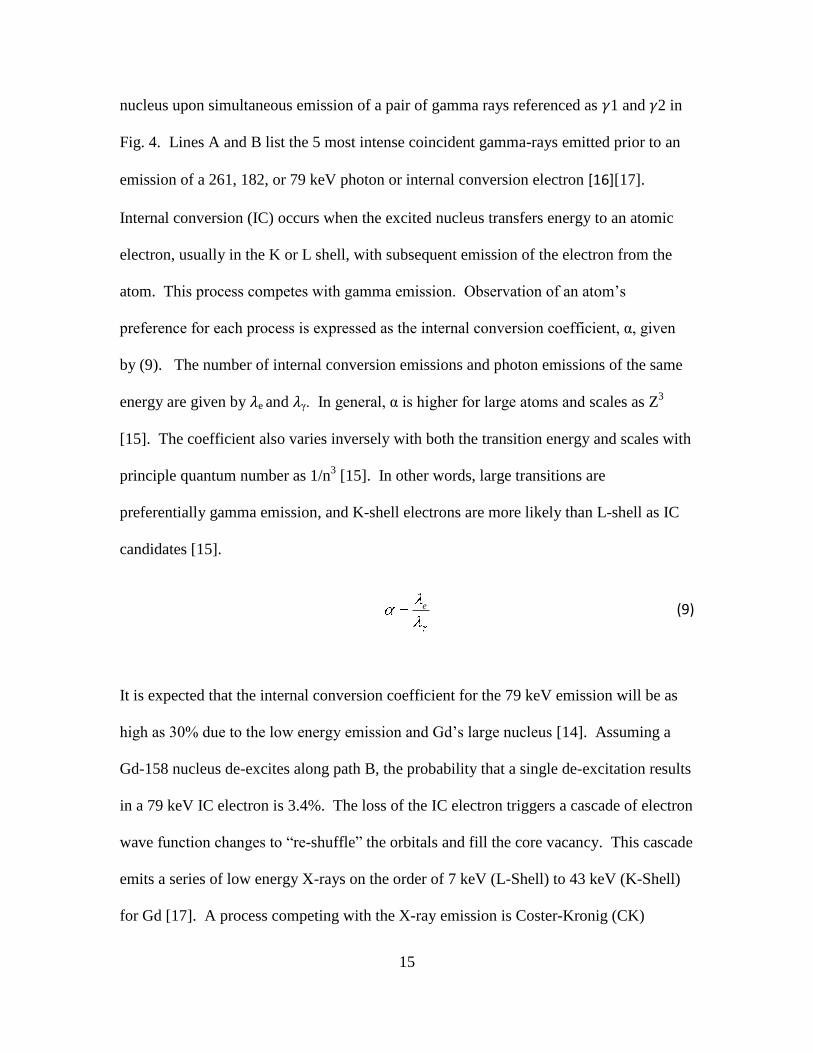
nucleus upon simultaneous emission of a pair of gamma rays referenced as 1 and 2 in
Fig. 4. Lines A and B list the 5 most intense coincident gamma-rays emitted prior to an
emission of a 261, 182, or 79 keV photon or internal conversion electron [16][17].
Internal conversion (IC) occurs when the excited nucleus transfers energy to an atomic
electron, usually in the K or L shell, with subsequent emission of the electron from the
atom. This process competes with gamma emission. Observation of an atom‟s
preference for each process is expressed as the internal conversion coefficient, α, given
by (9). The number of internal conversion emissions and photon emissions of the same
energy are given by e and γ. In general, α is higher for large atoms and scales as Z3
[15]. The coefficient also varies inversely with both the transition energy and scales with
principle quantum number as 1/n3 [15]. In other words, large transitions are
preferentially gamma emission, and K-shell electrons are more likely than L-shell as IC
candidates [15].
e (9)
It is expected that the internal conversion coefficient for the 79 keV emission will be as
high as 30% due to the low energy emission and Gd‟s large nucleus [14]. Assuming a
Gd-158 nucleus de-excites along path B, the probability that a single de-excitation results
in a 79 keV IC electron is 3.4%. The loss of the IC electron triggers a cascade of electron
wave function changes to “re-shuffle” the orbitals and fill the core vacancy. This cascade
emits a series of low energy X-rays on the order of 7 keV (L-Shell) to 43 keV (K-Shell)
for Gd [17]. A process competing with the X-ray emission is Coster-Kronig (CK)
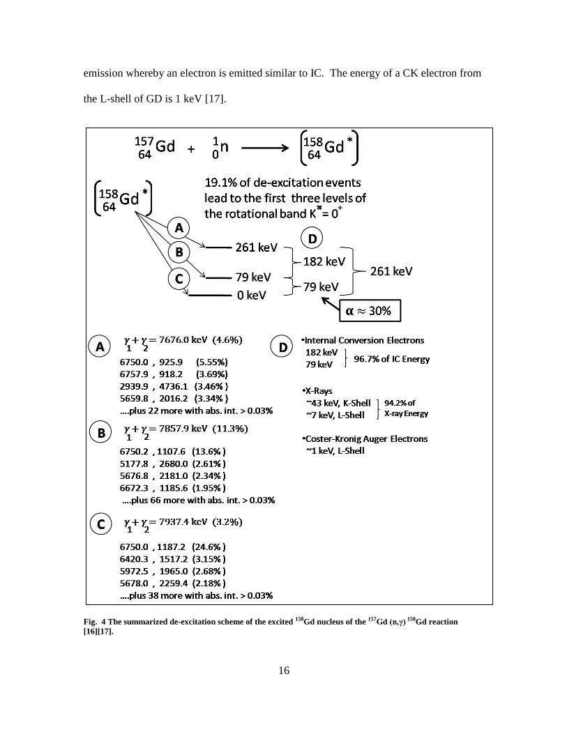
16
emission whereby an electron is emitted similar to IC. The energy of a CK electron from
the L-shell of GD is 1 keV [17].
Fig. 4 The summarized de-excitation scheme of the excited 158Gd nucleus of the 157Gd (n,γ) 158Gd reaction
[16][17].

17
III. EXPERIMENTAL APPROACH
3.1 Introduction
The experimental approach covers four areas. First, the application of a thin film
of Gd2O3 on p-type silicon using a supercritical water system is described. Next, the
fabrication of a diode from the deposition sample is explained. Third, the feasibility of
the device as a neutron detector is discussed. Lastly, the design of an experiment to
determine if the diode can successfully detect neutrons is presented.
3.2 Supercritical Gadolinium Oxide Deposition
Gadolinium oxide (Gd2O3, or gadolina) has been explored commercially as a
high-k dielectric to replace SiO2 in traditional metal-oxide-semiconductors. The use of a
high-k material provides a gate that is thicker than SiO2 but electrically equivalent, thus
reducing leakage currents [19]. As a result, the process of fabricating a semiconductor
from gadolina and silicon has been recently developed by the semiconductor industry
[19]. The advances have been in the interest of miniaturization, not neutron detection.
Diodes made from Gd2O3 deposited on p-type silicon have been successfully
fabricated at the University of Nebraska, Lincoln (UNL) by both pulsed laser deposition
(PLD) and supercritical water deposition. The use of pulsed laser deposition to deposit
gadolina on Si yielded a monoclinic Gd2O3 crystal structure. The use of supercritical
water deposition yielded a cubic Gd2O3 structure. Fig. 5 illustrates the arrangement of
the atoms in the two crystal structures.
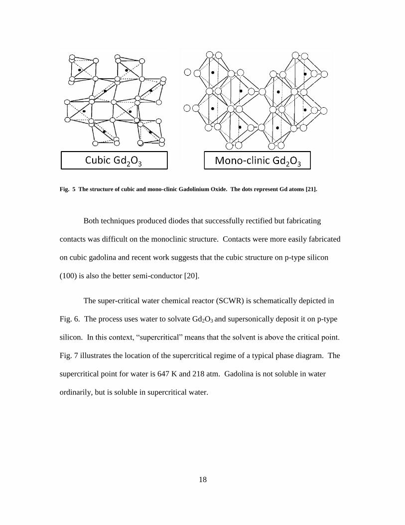
18
Fig. 5 The structure of cubic and mono-clinic Gadolinium Oxide. The dots represent Gd atoms [21].
Both techniques produced diodes that successfully rectified but fabricating
contacts was difficult on the monoclinic structure. Contacts were more easily fabricated
on cubic gadolina and recent work suggests that the cubic structure on p-type silicon
(100) is also the better semi-conductor [20].
The super-critical water chemical reactor (SCWR) is schematically depicted in
Fig. 6. The process uses water to solvate Gd2O3 and supersonically deposit it on p-type
silicon. In this context, “supercritical” means that the solvent is above the critical point.
Fig. 7 illustrates the location of the supercritical regime of a typical phase diagram. The
supercritical point for water is 647 K and 218 atm. Gadolina is not soluble in water
ordinarily, but is soluble in supercritical water.

19
Fig. 6 A schematic representation of the super-critical water chemical reactor (SCWR) successfully used at the
University of Nebraska, Lincoln to deposit cubic Gd2O3 on p-type silicon. (1) Purified Water Tank. (2) High
Pressure Pumps. (3) First Stage Solvent Heater. (4) Second Stage Solvent Heater. (5) Filter Basket containing
Gd2O3. (6) Expansion Nozzle and p-type silicon target. T1, T2, and T3 are temperature probes.
Fig. 7 A typical phase diagram of matter showing the location of the Critical Point, above which the material
acts as a supercritical fluid.

20
The deposition process requires solvent and target substrate preparation. Ultra-
filtration of de-ionized water is performed until the nominal resistivity is approximately
17 MΩ cm. Nitrogen gas is bubbled through the water to displace dissolved gases. The
silicon substrate sample is washed for 10 minutes in both acetone and ethanol using an
ultrasonic bath to remove organic surface contaminants. A 5% hydroflouric (HF) acid
etch is then used to remove a surface layer followed by a water rinse prepared as stated.
The system uses two parallel syringe pumps, each with a 266 mL capacity, to
provide high pressure water. Only one pump is used at a time for semi-continuous
operation. The primary heating coil is used to bring the water temperature into the super
critical region. The secondary heating coil is located next to the 0.5 micron sintered
stainless steel filter basket in which 0.9 g of Gd2O3 is loaded. The system is optimized to
create stagnation conditions within the filter basket. At the stagnation point, all of the
kinetic energy of the fluid is converted to pressure. The fluid saturates with Gd2O3 and is
expanded supersonically through a 50 micron orifice across a 1 to 2 cm air gap onto the
substrate.
Although the operating conditions of the reactor are varied as part of ongoing
research, there are some nominal operating conditions. The primary coil is operated at
600 ⁰C, the secondary at 460 ⁰C. In order to achieve stagnation conditions, the nozzle
temperature must be the product of 0.88 and the absolute temperature of the fluid in the
filter basket. This equation is summarized in (10) and is the result of thermodynamic
modeling by Dr. Jennifer Brand of the UNL Chemical Engineering Department who is
currently researching supercritical deposition methods.

21
0 0Nozzle Temperature [ C] 0.88 460 C 273.15 (10)
The silicon substrate is fixed to the sample holder. The sample holder is monitored for
temperature but no effort is made to apply heat or electrical bias. The average deposition
time is 1 hour with water flow rates nominally 7mL/min. The Gd2O3 is deposited as a
film on the substrate with rods and crystallites visible on the surface of the film under an
optical microscope inspection illustrated in Fig. 8.
Fig. 8 An optical microscope view of the Gd2O3 film showing the formation of crystallites.
Using a profilometer, it was determined that a 1 hour deposition yielded a 1000 Å film.
The film thickness peaks near the focal point of deposition and tapers at the edges. Table
V is a compendium of deposition parameters for the samples produced at UNL.

22
TABLE V Deposition conditions for the samples prepared at the University of Nebraska
Super-Critical Water Deposition Conditions
Ab
r. S
amp
le #
University of Nebraska
Sample #
Sta
gn
atio
n T
emp
[⁰C
]
Pre
ss.
[bar
]
No
zzle
Tem
p [
⁰C]
Su
bst
rate
Tem
p
[⁰C
]
No
zzle
-Su
bst
rate
Sp
acin
g [
cm]
Dep
osi
tio
n T
ime
[min
]
11 061509-MP-Gd2O3-pSi-11 455 240 * * 2 60
12 061209-MP-Gd2O3-pSi-12 450 240 340 48 2 60
21 061009-MP-Gd2O3-pSi-21 500 240 344 54 1 60
31 061009-MP-Gd2O3-pSi-31 470 240 355 60 1 60
JS XXXXXX-XX-Gd2O3-pSi-
JS * * * * * *
* Indicates the parameter is unknown
3.3 Diode Fabrication
After deposition, contacts were sputtered onto the sample in order to create a
working device. The samples of Gd2O3 on silicon were prepared using a contact mask
which has a 5-hole by 5-hole grid in a 1 cm square on the deposited side. Copper tape
was used to build-up layers to provide indirect contact and mask the surface to shield
from over-sputter. The samples were attached to a carousel using tape and glass
microscope slides to protect the sample from the carousel‟s rough surface. The loaded
carousel is placed upside down onto a spindle affixed to the sputter chamber lid and a
moveable shield is placed on the spindle such that it protects the samples from the targets.
Gold and aluminum targets were placed into the magnetron “gun” positions inside the
23
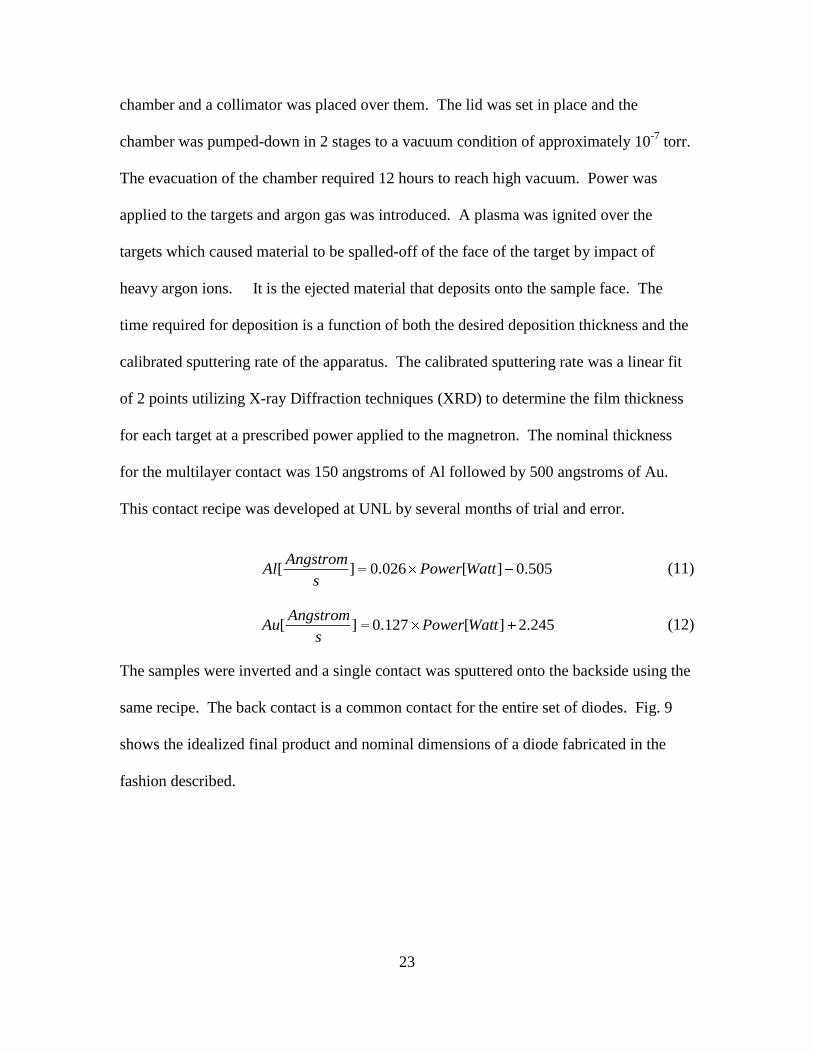
chamber and a collimator was placed over them. The lid was set in place and the
chamber was pumped-down in 2 stages to a vacuum condition of approximately 10-7
torr.
The evacuation of the chamber required 12 hours to reach high vacuum. Power was
applied to the targets and argon gas was introduced. A plasma was ignited over the
targets which caused material to be spalled-off of the face of the target by impact of
heavy argon ions. It is the ejected material that deposits onto the sample face. The
time required for deposition is a function of both the desired deposition thickness and the
calibrated sputtering rate of the apparatus. The calibrated sputtering rate was a linear fit
of 2 points utilizing X-ray Diffraction techniques (XRD) to determine the film thickness
for each target at a prescribed power applied to the magnetron. The nominal thickness
for the multilayer contact was 150 angstroms of Al followed by 500 angstroms of Au.
This contact recipe was developed at UNL by several months of trial and error.
[ ] 0.026 [ ] 0.505Angstrom
Al Power Watts
(11)
[ ] 0.127 [ ] 2.245Angstrom
Au Power Watts
(12)
The samples were inverted and a single contact was sputtered onto the backside using the
same recipe. The back contact is a common contact for the entire set of diodes. Fig. 9
shows the idealized final product and nominal dimensions of a diode fabricated in the
fashion described.

24
Fig. 9 A sample of Gd2O3 on Si with contacts. (A) A depiction of the sample with 25 contacts sputtered over the
Gadolina layer. (B) An end-view of the sample depicting the contact geometry (exaggerated dimensions). (C) A
dimensional depiction of the cross-section of a single diode using the base of the gold contact as a reference
point.
3.4 Initial Device Characterization
Characterization of the diodes was done to verify rectification. Fig. 10 illustrates
the current-voltage, or I(V), response of a single diode in sample 1, prepared from
061009-MP-Gd2O3-pSi-31, at various temperatures. The reverse bias region appears
relatively stable from 0 to -1V. The diode, modeled as Fig. 9 detail C, contains regions
of gadolina and silicon through which the charge carriers must move in order to reach the
contacts. The conductivity of the diode appears to decrease with decreased temperature
indicating that impurity scattering in the non-depleted regions is affecting conductivity.
Phonon scattering is not a contributing factor since decreased temperature decreases the
lattice vibration. The use of cold temperature conditions to reduce diode signal noise
would be offset by signal loss.

25
Fig. 10 The I(V) response for contact 5 of diode sample 1 showing rectification at various temperatures.
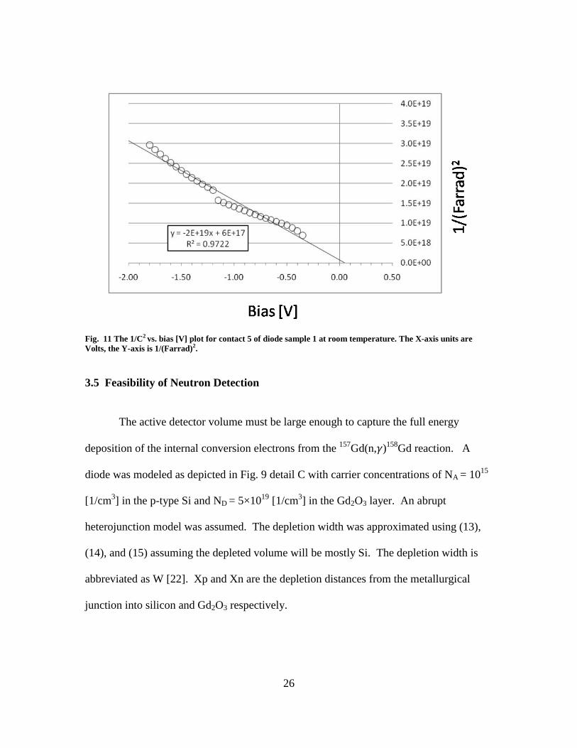
Capacitance-Voltage, C(V), measurements were conducted at room temperature
in order to determine the silicon substrate doping concentration and the threshold voltage.
A plot of 1/C2 vs. bias indicated a carrier concentration of 2 x 10
19 1/cm
3 which is suspect
for p-type silicon. Although the relatively linear plot indicates that an abrupt junction
approximation might be appropriate, the deposition method does not support it. The
junction will be sufficiently infused that C(V) data cannot be used to determine carrier
concentration. Intrinsic p-type silicon has a nominal carrier concentration of 1015
1/cm3
which was used for calculations to determine the depletion region boundaries.
26
Fig. 11 The 1/C2 vs. bias [V] plot for contact 5 of diode sample 1 at room temperature. The X-axis units are
Volts, the Y-axis is 1/(Farrad)2.
3.5 Feasibility of Neutron Detection
The active detector volume must be large enough to capture the full energy
deposition of the internal conversion electrons from the 157
Gd(n, )158
Gd reaction. A
diode was modeled as depicted in Fig. 9 detail C with carrier concentrations of NA = 1015
[1/cm3] in the p-type Si and ND = 5×10
19 [1/cm
3] in the Gd2O3 layer. An abrupt
heterojunction model was assumed. The depletion width was approximated using (13),
(14), and (15) assuming the depleted volume will be mostly Si. The depletion width is
abbreviated as W [22]. Xp and Xn are the depletion distances from the metallurgical
junction into silicon and Gd2O3 respectively.

27
2 2
0 2 3 0
( ) ( )( )
2( ) 2( )
A DBuiltIn applied
N q Xp N q XnV V
kSi kGd O (13)
W Xp Xn (14)
( ) ( )Xp Na q Xn Nd q (15)
The built-in voltage was taken as 0.15V which is the average value attained from the 1/C2
vs. bias plots for sample 1. The dielectric constant for Si, kSi, is 11.9 and 17 for Gd2O3,
kGd2O3. Solving (13) and (15) simultaneously for a bias of -1.5V yields a depletion width,
W, of 1.592 ×10⁻⁴
cm or 1592 nm. Assuming cylindrical geometry, the active volume of
the diode as a detector can be determined by assuming a diameter equal to the sputtered
contact region. Depicted in Fig. 12, the active volume of the detector is the region
straddling the metallurgical junction in which the full energy deposition of an IC electron
will result in a detected pulse.
Electrons produced by ionization outside of the depletion region are much less
likely to be collected out to a diffusion length away from the depletion region. Beyond a
diffusion length, the charge can be considered lost to the diode. The diffusion length of
an electron, Ln, in Si was computed to be 16 µm. Computing the active diode volume
using only the depletion width provides conservative results as the active volume is
somewhat larger.

28
Fig. 12 A graphical depiction of the active volume of the diode. The depletion region straddles the metallurgical
junction. The remaining parts of the diode are not shown but include the non-depleted Si and gadolina as well
as the contacts.
The diameter of a contact was measured to be 814×103 nm using a scaled enlargement of
the sputtered region. The resulting volume was calculated to be 4.14×10⁻⁶
cm3 using (16)
and is mostly silicon.
2( )( )
4
PX Contact DiameterActiveVolume (16)
The calculation of (13), (14), (15), and (16) using Mathematica® is included in
Appendix A [34].
A CASINO simulation was conducted to determine if the dimensions of the active
region were large enough to detect an IC electron [31]. The simulation output is
graphically shown in Fig. 13. The code simulates a monoenergetic electron beam of
specified energy traveling into a material which is silicon for this simulation. The color-
coded regions represent energy deposition in terms of initial energy. The outermost
contour is light blue and represents 5% of the initial energy, or 95% energy deposition.

29
Fig. 13 The graphical output of a Casino simulation showing (A) 79 keV electrons incident on a slab of Si with
full energy deposition in 40,000nm and (B) 180 keV electrons with full energy deposition in 160,000nm. The
outer contour line represents 5% of the incident energy.
With an active volume diameter of 814,000 nm, a 79 and 180 keV IC electron (ICe) will
both have the potential to be detected as a pulse. The 79 keV electrons in the CASINO
simulation deposited all of their energy in under 40,000 nm. The 180 keV electrons
deposited their total energy in 168,000 nm. Since the depletion width is only 1592 nm,
electrons with a trajectory parallel to the metallurgical junction will be able to deposit
their full energy as depicted in Fig. 14 detail C.
30
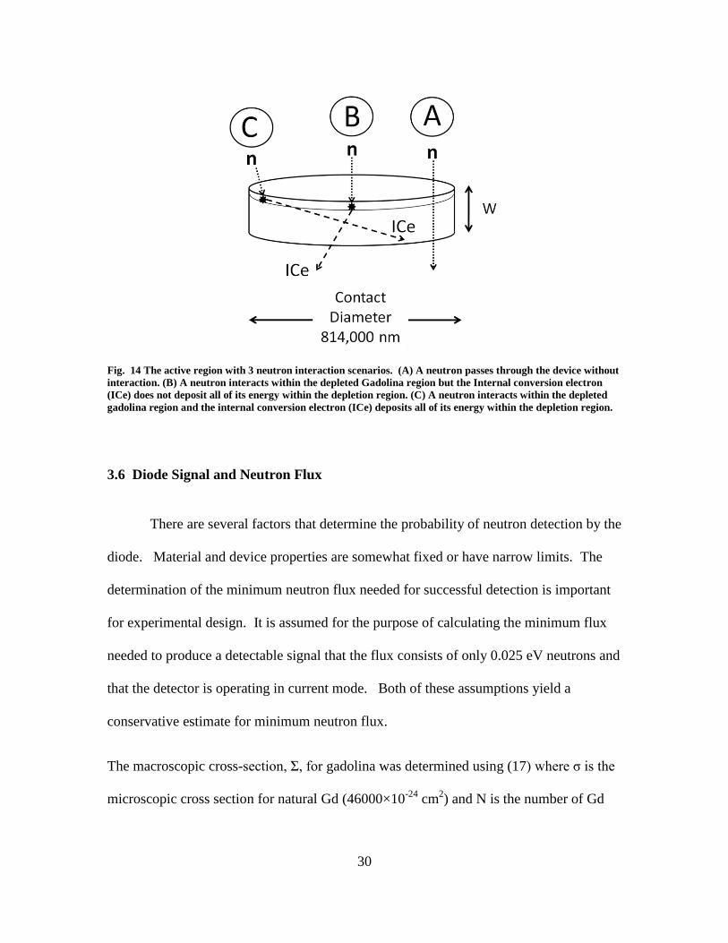
Fig. 14 The active region with 3 neutron interaction scenarios. (A) A neutron passes through the device without
interaction. (B) A neutron interacts within the depleted Gadolina region but the Internal conversion electron
(ICe) does not deposit all of its energy within the depletion region. (C) A neutron interacts within the depleted
gadolina region and the internal conversion electron (ICe) deposits all of its energy within the depletion region.
3.6 Diode Signal and Neutron Flux
There are several factors that determine the probability of neutron detection by the
diode. Material and device properties are somewhat fixed or have narrow limits. The
determination of the minimum neutron flux needed for successful detection is important
for experimental design. It is assumed for the purpose of calculating the minimum flux
needed to produce a detectable signal that the flux consists of only 0.025 eV neutrons and
that the detector is operating in current mode. Both of these assumptions yield a
conservative estimate for minimum neutron flux.
The macroscopic cross-section, Σ, for gadolina was determined using (17) where σ is the
microscopic cross section for natural Gd (46000×10-24
cm2) and N is the number of Gd

31
nuclei per volume given by (18) to be 2.53×10²²
Gd nuclei/cm3. MWGd2O3 represents the
molecular weight of gadolina, and ρGd2O3, its density.
N (17)
2 3
2 3 2 3
( )( )
Gd O Avogadro
Gd O
N molesGdN
MW moleGd O (18)
The reaction rate density (RRD) was then computed by (19) which is the product of the
macroscopic cross-section and the neutron flux.
RRD (19)
The expected electrical signal (EES) is the product of the RRD, active detector volume,
average crystal ionization energy, and the probabilities of producing an ICe. The EES is
summarized in (20).
e ICe
Branch
ionization
q EEES RRD Vol
E (20)
The term Vol is the active detector volume, γBranch is the probability of de-excitation to a
specific energy state, α is the internal conversion coefficient, qe is the charge of an
electron, EICe is the energy of the IC electron, and Eionization is the average energy required
to create an electron/hole pair in the material. The average ionization energy for gadolina
was approximated as 18 eV which is the value of SiO2. Fig. 15 shows the EES as a
function of thermal neutron flux calculated from (20) using the factors of Table VI. The
result indicates that a thermal neutron flux of 1x10⁶ [n/cm
2 s] is barely adequate to
achieve a reasonable signal. However, this is a conservative estimate in that it does not
consider that the charge is integrated over a pulse of a micro-second or less, producing a

32
stronger signal. This is termed „pulse mode‟ operation and is common to most
spectroscopic measurement systems [8]. Conservatively, the calculation shows that non-
reactor neutron sources could be used which simplified experimental design.
TABLE VI Parameters used to calculate the expected electrical signal.
Factor Constant Units
ρ Gd2O3 7.41 g/cm3
MW Gd2O3 352 g/mole
Vol 4.14x10⁻⁴
mm3
σ Gd 46000 b
α 30 %
γBranch 11.3 %
Eionization 18 eV
EICe 79,000 eV
Fig. 15 A plot of the expected electrical signal from the active volume (Left-Side) and a pre-amplifier output
voltage (Right-Side) as function of thermal neutron flux for the 79 keV ICe. The conversion of current to
voltage uses the factor of 0.64 µV per electron hole pair which is typical of the Amptek A250CF preamplifer.
33
3.7 Experimental Concept
3.7.1 Goal
The goal of the experiment was to determine if a semiconducting diode made
from gadolinium oxide (Gd2O3) and p-type silicon could detect neutrons. The theory and
modeling supported that the diode could produce a detectable electrical signal based upon
the 157
Gd(n, )158
Gd reaction. An investigation of a gadolinium-containing diode in 2008
claimed to have identified the 79 keV signal pulse [14]. This diode contained hafnium
oxide enriched with gadolinium up to 15%. A diode fabricated with Gd2O3 should
produce a larger signal corresponding to a higher reaction rate density.
3.7.2 Coincidence Measurements
In order to determine if the detected signal was from the 157
Gd(n, )158
Gd reaction,
coincident gamma emissions were to be used in order to corroborate the claim of neutron
detection. The 6750.2/1107.6 keV binary gamma ray pair is the most likely emission in
coincidence with a 79 keV ICe. Large diameter sodium-iodide (NaI) detectors were
readily available but did not have the resolution to discriminate between the 1107.6 keV
and 1187.2 keV gamma ray emissions, the two most likely emissions. The resolution of
an energy feature in a pulse-height spectrum can be represented as the full-width at half
maximum (FWHM) of the energy divided by the centroid (H0) energy. Resolution can
also be represented as a proportionality constant, K, divided by the square root of energy
as in (21) [8].
34
0
FWHM KR
H E (21)
Using a nominal K value for NaI of 3.14 [8], the resolutions for energies of 1187 and
1107 keV are 9.1% and 9.4%. The peaks for these centroids would overlap at FWHM by
5 keV if a NaI detector were used. Cerium doped Lanthanum Bromide, LaBr(Ce),
scintillators have a resolution as high as 3% at 662keV which will provide the appropriate
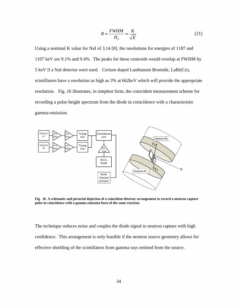
resolution. Fig. 16 illustrates, in simplest form, the coincident measurement scheme for
recording a pulse-height spectrum from the diode in coincidence with a characteristic
gamma-emission.
Fig. 16 A schematic and pictorial depiction of a coincident detector arrangement to record a neutron capture
pulse in coincidence with a gamma emission born of the same reaction.
The technique reduces noise and couples the diode signal to neutron capture with high
confidence. This arrangement is only feasible if the neutron source geometry allows for
effective shielding of the scintillators from gamma rays emitted from the source.

35
3.7.3 Neutron Source
Two 5 Ci Plutonium-Beryllium (PuBe) sources were available as a source of
neutrons. The PuBe source is a mixture of Pu and Be completely mixed together and
sealed in a stainless steel casing. The decay of Pu produces an alpha particle as shown in
(22) and (23) which interact with the Be to produce a neutron (26). The presence of Pu-
241 which decays to Am-241 shown as (24) provides an increasing neutron emission rate
for several years after the production of the source.
4
1/2 2.4 10239 235 4
94 92 2
t yearsPu U (22)
1/2 87.8238 234 4
94 92 2
t yearsPu U (23)
1/2 14.4241 241
94 95
t yearsPu Am (24)
1/2 433241 237 4
95 93 2
t yearsAm Np (25)
9 4 0 12
4 2 6Be n C (26)
Calculating the neutron emission rate of a PuBe source requires the use of the Bateman
equations for the decay reactions listed above. This calculation was performed by [30]
and a modified calculation is included in Appendix C. The neutrons born of the
reaction are fast and must be moderated to produce a sizeable thermal
neutron population. A neutron howitzer provides neutron moderation and allows for the
construction of a coincident gamma-ray detection system. Using paraffin wax as the
howitzer moderator is simple, cost effective, and efficient. Stoichiometrically, paraffin
can be modeled as C32H68 and has a density of 0.93 g/cm3 [23]. The large fraction of

36
hydrogen makes it an excellent moderator material. The construction of two howitzers
would allow for the use of both 5 Ci PuBe sources as depicted in Fig. 17.
Fig. 17 A simplified scheme of using tandem “neutron howitzers” powered by PuBe sources to irradiate a
sample diode with thermalized neutrons.
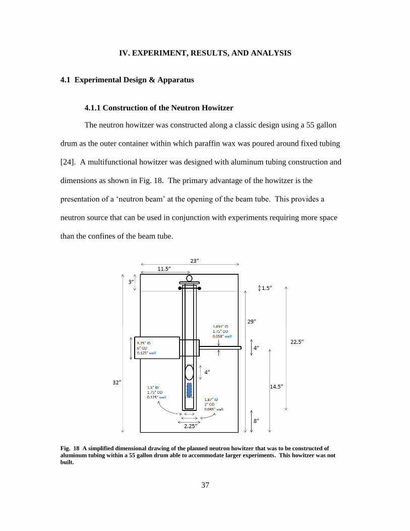
37
IV. EXPERIMENT, RESULTS, AND ANALYSIS
4.1 Experimental Design & Apparatus
4.1.1 Construction of the Neutron Howitzer
The neutron howitzer was constructed along a classic design using a 55 gallon
drum as the outer container within which paraffin wax was poured around fixed tubing
[24]. A multifunctional howitzer was designed with aluminum tubing construction and
dimensions as shown in Fig. 18. The primary advantage of the howitzer is the
presentation of a „neutron beam‟ at the opening of the beam tube. This provides a
neutron source that can be used in conjunction with experiments requiring more space
than the confines of the beam tube.
Fig. 18 A simplified dimensional drawing of the planned neutron howitzer that was to be constructed of
aluminum tubing within a 55 gallon drum able to accommodate larger experiments. This howitzer was not
built.

38
The actual howitzer was built using PVC pipe due to time constraints. Fig. 19 shows the
dimensions of the simplified design.
Fig. 19 The dimensions of the Neutron howitzer as built with PVC pipe. The cross-section of the howitzer as
see from the side is shown in „A.‟ The details of the fixed central tube and moveable inner tube are shown in „B.‟
„C‟ shows the detail of the inner tube as observed with the same aspect of „A‟,‟B‟, and „C‟. „D‟ shows the inner
tube with the source opening rotated 90 degrees toward the observer. Details „B‟,‟C‟, and „D‟ are drawn to
scale. „A‟ is not to scale and represents the dimensions of a 55 gallon drum.
The howitzer is loaded in 3 steps: 1) Raise and rotate the inner tube to the „load‟
position and partially insert the positioning peg 2) Remove the PuBe source from the
storage container and place it into the recess of the inner tube using a remote handling
tool 3) Remove the positioning peg and allow the inner tube containing the source to

39
drop into the safe position under its own weight. The source can be raised to the „beam‟
position when needed.
The construction of the howitzer was straight forward. The PVC pipe was cut to
length and the source opening was cut and shaped. Wooden plugs were cut to seal the
bottom of the fixed center tube as well as the top and bottom of the inner tube where the
source is housed. Care was used to make sure that the top of the source access hole was
flush with the bottom of the wooden plug. A lip at this location could cause the source to
„stick‟ in the tube during removal. Fig. 20 shows the working components of the
howitzer during pre-assembly. A hole matching the outer diameter of the beam tube was
drilled in the 55 gallon drum. The pipe and fittings were assembled inside the drum and
fixed using a wooden foot anchored to the bottom of the drum.
Fig. 20 The Neutron Howitzer PVC components. „A‟ The moving and fixed tubes with pieces of wood
indicating the thickness and location of the plugs inside the inner tube. „B‟ A detail of the source holder as well
as the bottom of the center tube which is a clean-out that is to be anchored inside the drum.

40
Fig. 21 illustrates the final assembly of the howitzer with paraffin. Small propane camp
stoves were used to melt the wax which was then poured into the howitzer. Paraffin wax
melts between 135 and 145⁰ F and has a flash-point between 248 and 254⁰ F making it a
safe product to work with. The howitzer required approximately 500 pounds of paraffin
to fill.
Fig. 21 The final assembly of the Neutron Howitzer. „A‟ Camp stoves were used to melt the paraffin wax
outdoors. „B‟ The PVC tubes anchored into the drum and a few inches of wax. „C‟ The wax had to be melted a
few ounces at a time. Maintaining liquid wax in the melt was important for heat transfer. „D‟ Uneven cooling of
the wax produced contraction pockets which were filled with wax in subsequent pours.
The wax was poured over several days outdoors with ambient temperatures in the 40 to
60 ⁰F range. The first day of work filled the drum up to ~18 inches from the bottom. A
leak developed around the beam tube which was sealed by allowing a cylinder of wax to
partially cool and forming it around the seam like a putty. Subsequent pours melted the
previously cooled wax with each addition to the drum. On the second day of work, it was
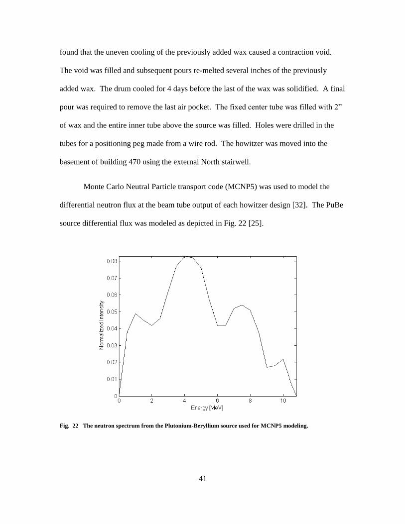
41
found that the uneven cooling of the previously added wax caused a contraction void.
The void was filled and subsequent pours re-melted several inches of the previously
added wax. The drum cooled for 4 days before the last of the wax was solidified. A final
pour was required to remove the last air pocket. The fixed center tube was filled with 2”
of wax and the entire inner tube above the source was filled. Holes were drilled in the
tubes for a positioning peg made from a wire rod. The howitzer was moved into the
basement of building 470 using the external North stairwell.
Monte Carlo Neutral Particle transport code (MCNP5) was used to model the
differential neutron flux at the beam tube output of each howitzer design [32]. The PuBe
source differential flux was modeled as depicted in Fig. 22 [25].
Fig. 22 The neutron spectrum from the Plutonium-Beryllium source used for MCNP5 modeling.

42
The moderated spectrum at the beam tube output, as modeled in MCNP, is graphically
depicted in Fig. 23 for the neutron population below 1 eV. The input code for this
simulation is found in Appendix D.
Fig. 23 The differential neutron flux at the beam tube output of the PuBe source for the two neutron howitzer
designs.
Because the lowest energy of the PuBe spectrum was modeled as 0.5 MeV, it is believed
that the model produced conservative results since the differential neutron flux of the
PuBe source does have a low energy component which would add to the population of
Fig. 23. The „normalized intensity‟ is a model output parameter that can be thought of as
the probability per source neutron, PPSN. It is the fraction per emitted source neutron
43
that would be present at the modeled location. For example, the output of the PuBe
source in December of 2009 was approximately 1.14 × 10⁷
n/s according to Appendix C.
The howitzer output with PVC construction should yield a 0.1 eV flux of approximately
500 n/cm2 s which results from multiplying the neutron activity by the normalized
intensity of ~4.5 × 10⁻⁵
.
4.1.2 Coincident Gamma-Ray Instrumentation Scheme
In order to add credibility to the detection of a neutron pulse, LaBr(Ce) scintillation
detectors were emplaced to provide a gate signal to the multi-channel buffer (MCB)
when an 1107.6 keV gamma ray was detected. An 1107.6 KeV emission corresponds to
an excited Gd-158 nucleus emitting a pair of gamma-rays of energy 6750.2 and 1107.6
keV. It is known that, of the 19.1% of the Gd-158 de-excitations following neutron
capture, 11.3% will result in the sum emission of 7857.9 keV which will be the
mentioned binary pair 13.6% of the time (See Fig. 4). The initial instrument scheme was
established as illustrated in Fig. 24. It was discovered that the PMTs integrated with the
scintillators had a significantly different response and that the use of only one Single
Channel Analyzer (SCA) would not work.

44
Fig. 24 The initial instrument scheme for coincident measurement. The unequal response of the PMTs
prompted experimenting with separate power supplies but this arrangement was eventually changed to employ
separate SCAs. The linear amplifier provides the power for the pre-amplifier.
The use of separate power supplies was employed in order to adjust the PMT bias
separately to synchronize the response. This was eventually abandoned in favor of the
dual linear amplifier and SCA circuit shown as Fig. 25.

45
Fig. 25 The final instrument scheme for coincident measurement. The use of separate amplifiers and SCAs
allowed each scintillator circuit to be calibrated to send a gate pulse upon the detection of an 1107.6 keV event.
A digital signal from either SCA provided the Multi-Channel Buffer (MCB) with a gate
signal. The MCB would only accept an analog signal from the diode when a gate pulse
was present. The delay line amplifiers (DLA) in the scheme are needed to compensate
for the delay in receiving the gamma signal and the collection of the diode signal
following a neutron capture. The gate and delay module allowed for amplitude and
duration adjustments of the gate signal fed to the MCB. A bench-test of the system using
a pulser and a Co-60 source was conducted to proof the scheme and roughly calibrate the
delay required in each leg. The test arrangement is depicted in Fig. 26.
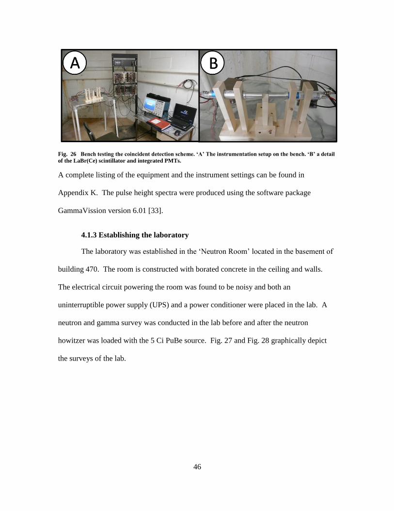
46
Fig. 26 Bench testing the coincident detection scheme. „A‟ The instrumentation setup on the bench. „B‟ a detail
of the LaBr(Ce) scintillator and integrated PMTs.
A complete listing of the equipment and the instrument settings can be found in
Appendix K. The pulse height spectra were produced using the software package
GammaVission version 6.01 [33].
4.1.3 Establishing the laboratory
The laboratory was established in the „Neutron Room‟ located in the basement of
building 470. The room is constructed with borated concrete in the ceiling and walls.
The electrical circuit powering the room was found to be noisy and both an
uninterruptible power supply (UPS) and a power conditioner were placed in the lab. A
neutron and gamma survey was conducted in the lab before and after the neutron
howitzer was loaded with the 5 Ci PuBe source. Fig. 27 and Fig. 28 graphically depict
the surveys of the lab.

47
Fig. 27 A schematic of the laboratory depicting the results of the gamma radiation survey before and after
loading the howitzer. „A‟ indicates background gamma levels prior to loading the howitzer, „B‟ indicates the
levels after loading with the source in the beam position. Location 8 is a lead box housing a small Co-60 test
source.
Fig. 28 A schematic of the laboratory depicting the results of the neutron radiation survey before and after
loading the howitzer. „A‟ indicates levels prior to loading the howitzer, „B‟ indicates the levels after loading with
the source in the beam position.
The WPAFB Radiation Safety Office conducted an independent survey of the lab and
surrounding basement area and concluded that this laboratory setup did not pose a risk to
non-research personnel working in the basement.

48
4.2 Calibration of the Coincident Gamma-Ray Instrumentation
Each scintillator „leg‟ of the coincident detection scheme was independently
calibrated using a pulser and a Co-60 source that provided 2 readily identifiable peaks at
1173.237 and 1332.501 keV. After establishing the amplification settings that placed the
Co-60 peaks near the midpoint (5V) of the pulse-height spectrum (PHS), an amplified
pulser signal of known amplitude was fed into each SCA. The output of the SCA was fed
into a counter module as illustrated in Fig. 29.
Fig. 29 The SCA configuration calibration scheme. The pulser signal could be used without amplification, but
the amplified pulser signal emulates the shaping effects found in the detector signal for a more accurate
calibration.
With the SCA in normal mode, the upper and lower adjustment knobs were used to find
the point at which the SCA stopped sending a digital pulse to the counter. The same
pulser signal was sent to the MCB and the centroid of the peak was determined. A
nearly-linear relationship was determined between the signal amplitude, PHS channel,
and SCA dial settings. For the same amplification settings, a Co-60 PHS provided a 2
point energy calibration that was used to determine the channel at which an 1107.6 keV
pulse would bin. To this channel was added half the number of channels required to
reach the centroid of the 1187.2 keV peak. This is next most likely peak emitted as a
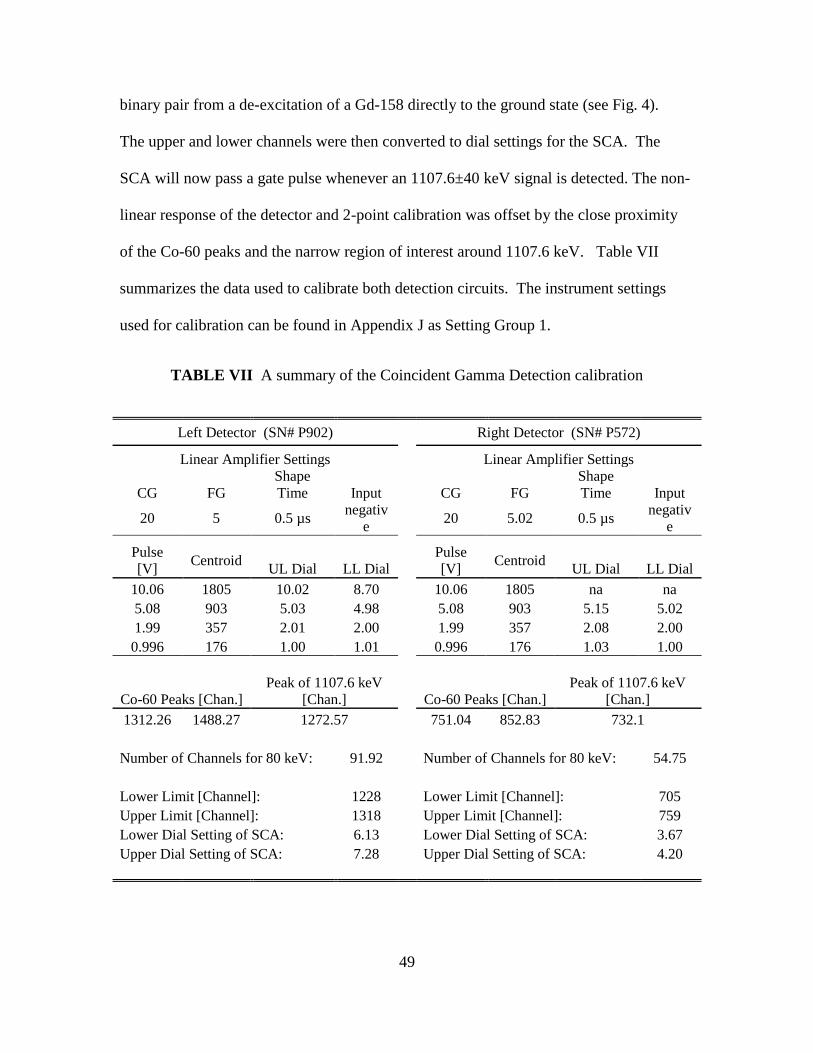
49
binary pair from a de-excitation of a Gd-158 directly to the ground state (see Fig. 4).
The upper and lower channels were then converted to dial settings for the SCA. The
SCA will now pass a gate pulse whenever an 1107.6±40 keV signal is detected. The non-
linear response of the detector and 2-point calibration was offset by the close proximity
of the Co-60 peaks and the narrow region of interest around 1107.6 keV. Table VII
summarizes the data used to calibrate both detection circuits. The instrument settings
used for calibration can be found in Appendix J as Setting Group 1.
TABLE VII A summary of the Coincident Gamma Detection calibration
Left Detector (SN# P902)
Right Detector (SN# P572)
Linear Amplifier Settings
Linear Amplifier Settings
CG FG Shape
Time Input
CG FG Shape
Time Input
20 5 0.5 µs negativ
e 20 5.02 0.5 µs
negativ
e
Pulse
[V] Centroid
UL Dial LL Dial
Pulse
[V] Centroid
UL Dial LL Dial
10.06 1805 10.02 8.70
10.06 1805 na na
5.08 903 5.03 4.98
5.08 903 5.15 5.02
1.99 357 2.01 2.00
1.99 357 2.08 2.00
0.996 176 1.00 1.01
0.996 176 1.03 1.00
Co-60 Peaks [Chan.] Peak of 1107.6 keV
[Chan.]
Co-60 Peaks [Chan.] Peak of 1107.6 keV
[Chan.]
1312.26 1488.27 1272.57
751.04 852.83 732.1
Number of Channels for 80 keV: 91.92
Number of Channels for 80 keV: 54.75
Lower Limit [Channel]: 1228
Lower Limit [Channel]: 705
Upper Limit [Channel]: 1318
Upper Limit [Channel]: 759
Lower Dial Setting of SCA: 6.13
Lower Dial Setting of SCA: 3.67
Upper Dial Setting of SCA: 7.28
Upper Dial Setting of SCA: 4.20
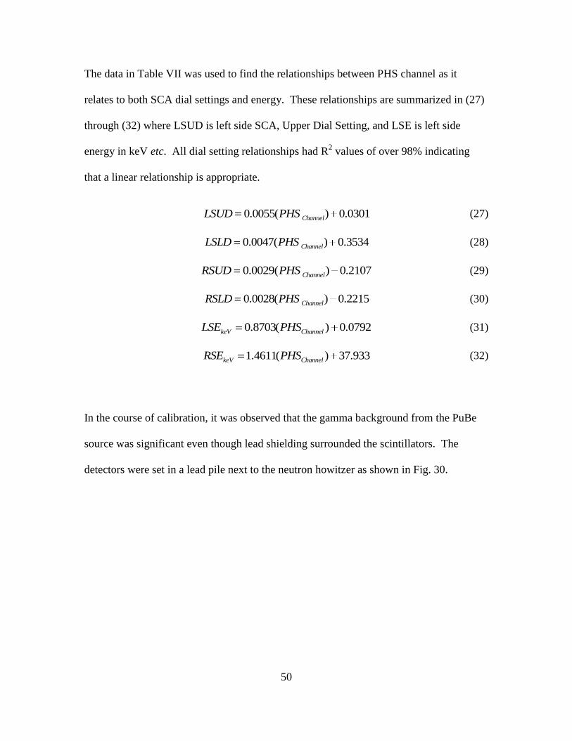
50
The data in Table VII was used to find the relationships between PHS channel as it
relates to both SCA dial settings and energy. These relationships are summarized in (27)
through (32) where LSUD is left side SCA, Upper Dial Setting, and LSE is left side
energy in keV etc. All dial setting relationships had R2 values of over 98% indicating
that a linear relationship is appropriate.
0.0055( ) 0.0301ChannelLSUD PHS (27)
0.0047( ) 0.3534ChannelLSLD PHS (28)
0.0029( ) 0.2107ChannelRSUD PHS (29)
0.0028( ) 0.2215ChannelRSLD PHS (30)
0.8703( ) 0.0792keV ChannelLSE PHS (31)
1.4611( ) 37.933keV ChannelRSE PHS (32)
In the course of calibration, it was observed that the gamma background from the PuBe
source was significant even though lead shielding surrounded the scintillators. The
detectors were set in a lead pile next to the neutron howitzer as shown in Fig. 30.

51
Fig. 30 A lead shield was constructed next to the neutron howitzer as shown in „A‟. „B‟ is a view of the lead
pile from behind the howitzer. Visible are two pieces of PVC pipe that contain the LaBr detectors opposing each
other. Lead would normally cover the top of the channel but it was removed for the photo. The beam tube is
centered on the channel containing the block of wood which was used as a stand to raise the Co-60 source closer
to the detectors. Also visible in „B‟ is the Co-60 source and a bottle of Gadolinium Oxide.
The initial shielding around the LaBr detectors was 4” of lead. The nominal activity of
the PuBe source is 5 Ci, or 1.85 × 10¹¹
gammas per second. Using the average gamma
energy value of 200 keV, the 10th thickness of lead is 0.08”. Achieving a 1010
reduction
of the average gamma intensity required 10” of lead. The lead shielding was re-built to
provide 12” of lead between the PuBe source and the scintillators. The background
decreased as expected. Fig. 31 shows a comparison of the pulse-height spectra using
both a 4” and 12” lead shield. The spectra agree with published photon spectra of PuBe
sources [26].

52
Fig. 31 The pulse-height spectrum taken with the LaBr detectors at the diode location in the lead shielding next
to the neutron howitzer. The counting interval was 3600s (1 hr) of live time.
A Co-60 source was used to provide an energy reference in order to identify the region of
interest for the 1107.6 keV peak. Fig. 32 is an example of a pulse-height spectrum of the
PuBe gamma background with a Co-60 spectrum overlaid. The peak amplitudes for
comparison are somewhat arbitrary due to different sample times, but the Co-60 peaks in
this spectrum are clearly visible at channels 777 and 886. Using the calibration
procedure previously presented, the centroid of the 1107.6 keV peak would be expected
in channel 732.
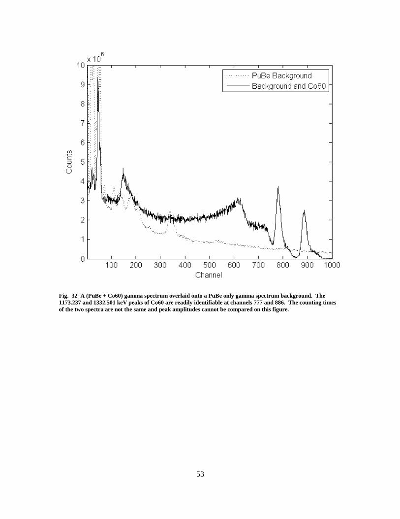
53
Fig. 32 A (PuBe + Co60) gamma spectrum overlaid onto a PuBe only gamma spectrum background. The
1173.237 and 1332.501 keV peaks of Co60 are readily identifiable at channels 777 and 886. The counting times
of the two spectra are not the same and peak amplitudes cannot be compared on this figure.
54
4.3 Neutron Detection Experiment using Neutron Howitzer
The diodes were ruggedized for experimentation by fixing the wafer containing
the diodes onto a plastic frame. Metal leads were set into the plastic frame to which gold
wires were affixed, terminating at the diode contacts. Silver paint was used to make
these connections. Wire was soldered to the leads on the outside of the plastic frame.
The wires were connected in parallel and terminated with a BNC connector. Prior to
assembly, each diode was verified for rectification by observing the I(V) response using a
Kiethley 4200 SCS. After assembly, each diode was again verified for rectification to
ensure all contacts were acceptable. Three diode samples were prepared, each containing
4 to 6 individual diodes in parallel to increase the detector volume as depicted in Fig. 33.
The samples were placed between the LaBr scintillators as closely as possible to
maximize geometric efficiency as pictured in Fig. 34.

55
Fig. 33 Three diode samples were prepared for experimentation. Diode 3, shown in „C‟ had the best
characteristics and was used for all experimentation.
Fig. 34 The diodes were placed as close to the LaBr crystals as possible to maximize the geometric efficiency.
„B‟ is a close-up of the diode sample mount showing the gold wires leading from the diode contacts.

56
The samples were connected to 1 of 2 different powered pre-amps in an AC coupled
mode. An ORTEC Model 142IH pre-amp was used as well as an Amptek A250CF
which is self-cooled and has exceptionally low noise characteristics. The bias was
provided through the pre-amp from a Mastech HY3006D digital power supply set at -
1.500 V. The pre-amp signal was output to an ORTEC 572A linear amplifier which was
set at the lowest gain, nominally a factor of 10. The amplifier contains an active filter
circuit and requires a shaping time input which is nominally the time required for the
detector to collect a pulse. The charge collection time was calculated by determining the
electron velocity within the active detection region of the diode. Because the majority of
the depleted region is silicon, the electron mobility was taken as 1400 × 10-4
m2/V s and
the relative permeability as 11.68. The electron velocity was calculated from (33) where
V is the drift velocity, µ is the mobility, and ε is the electric field. The field is
represented by (34). The distance, d, is the region over which the bias generates a field.
This distance, taken as 0.7 µm, is graphically depicted in Fig. 35 as the region of energy
band „bending‟ in the heterojunction band structure model.
n nV (33)
Bias
d k (34)

57
Fig. 35 A simple band structure model of the Gd2O3/Si heterojunction. The electric field created by the
applied bias is limited to a region approximately 0.7 µm in length.
The distance over which the electrons must move in order to be collected is the diffusion
length of an electron in p-Si. Taking the effective mass of an electron as 26% of the
electron rest mass m0, the electron recombination time, τn, is determined by (35) where q
is the electronic charge [22]. In practice, this is a difficult factor to determine and was
taken to be 1 µs which is a nominal value for p-Si.
0(0.26) nn
m
q (35)
The diffusivity, Dn, was calculated using (36) assuming a temperature of 300K. The
diffusivity is 3.6 × 10³ m
2/s.
n n
kTD
q (36)
The diffusion length, Ln, is calculated by (37) once diffusivity and the recombination
time are known. The diffusion length was determined to be approximately 60 µm.
( )n n nL D (37)
58
The time required to collect a pulse is then the length the electrons travel to the depletion
region divided by their velocity depicted as (33). The collection time was found to be 0.3
µs using (38). The lowest shaping time constant of 0.5 µs was selected.
n
n
LCollection Time
V (38)
In order to calculate the time required to observe neutron pulses in coincidence with
detected 1107.6 keV gamma rays, the reaction rate was calculated assuming a thermal
neutron flux of 500 /cm2 s and 5 diodes wired in parallel. The reaction rate was
calculated using (39) where ϕ is the thermal neutron flux, σ, is the thermal neutron cross-
section for absorption, and #Gd is the number of Gadolinium nuclei in the active region
of the diode.
Reaction Rate (# )Gd (39)
The reaction rate was determined to be 2.42 reactions per second. In order to determine
the rate at which 1107.6 keV gammas may be detected in coincidence with a neutron
capture, the rate is multiplied by several factors. First, the known de-excitation fractions
from Fig. 4 and the internal conversion coefficient (30%) are applied to the reaction rate
(39) to find the rate at which 79 keV internal conversion electrons are produced
simultaneously with coincident 1107.6 keV gamma emissions.
Rate of coincident emissions = Reaction Rate 0.113 0.136 0.30 (40)
The rate of coincident emissions was found to be 0.0056 per second. To this rate, an
efficiency factor is applied for the LaBr detectors. The geometric efficiency was

59
determined by using the solid angle between the detectors and the diode. This quantity
was calculated to be 0.132 using two 0.18 cm diameter LaBr crystals spaced 0.75 and 0.1
cm away from the diode. Because there is no published efficiency data available for
these detectors at the energy of interest, the geometric efficiency was taken as the total
efficiency. The final factor is the number of internal conversion electrons that will not
deposit an appreciable amount of their energy within the active volume. A first order
estimate for this value is 0.25 which is only a qualitative value. A more rigorous
approach to determine this value using a numerical model was not performed.
Multiplying the rate of coincident emissions by the geometric efficiency and fraction of
lost internal conversion electrons yields 0.00018 countable events per second. In order to
count 100 neutron capture events capable of being detected by coincident gamma
emission, it would require 6.3 days of counting. The details of this calculation can be
found in Appendix A.
In order to increase the reaction rate and validate the scintillator instrumentation,
a bottle of gadolinum oxide was placed between the detectors. This provided a Gd target
for neutrons in order to provide a large number of neutron interactions and subsequent
emission of 1107.6 keV gammas. This energy peak was expected to have a higher
intensity than the other known lines from the de-excitation of meta-stable Gd-158 as
depicted in Fig. 4. However, the energy peak was not identified above the background
using the 12” thick lead shielding arrangement. It could roughly be expected that the
neutron flux would be diminished by 1/9 when the shielding was increased from 4” to
12”. In an effort to increase the neutron flux, the shielding was reduced to 4” and the
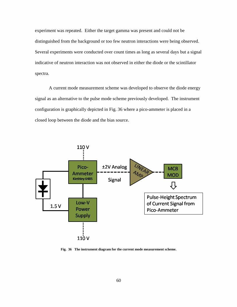
60
experiment was repeated. Either the target gamma was present and could not be
distinguished from the background or too few neutron interactions were being observed.
Several experiments were conducted over count times as long as several days but a signal
indicative of neutron interaction was not observed in either the diode or the scintillator
spectra.
A current mode measurement scheme was developed to observe the diode energy
signal as an alternative to the pulse mode scheme previously developed. The instrument
configuration is graphically depicted in Fig. 36 where a pico-ammeter is placed in a
closed loop between the diode and the bias source.
Fig. 36 The instrument diagram for the current mode measurement scheme.

61
This arrangement records the average current as developed over many pulses. The
Kiethley 6485 Pico-Ammeter was set to operate in the nano-amp range with a 2 nA full
scale setting. This provided an analog output representing 2.1 nA as a full 2V signal
which was input to the linear amplifier set at a gain of 1500. The instrument settings can
be found in Appendix J under Group 2. This high-gain regime allowed for the use of a
larger portion of the MCB channels but also caused a high dead time which was reduced
by setting the low level discriminator on the MCB to 2.28V. The instrument settings
used for this experiment can be found in Appendix J as Setting Group 2. A splitter box
was constructed in order to maintain the use of coaxial cables and connect the devices as
described. A diagram and picture of the splitter box is shown in Fig. 37.
Fig. 37 The current mode experiment required a splitter box in order to continue the use of coaxial cables and
BNC connectors.
A pulse-height spectrum produced in accordance with Fig. 36 represents an average
current value measured by the ammeter multiple times over the counting period. After
the instrumentation was established, a system noise measurement was made by turning
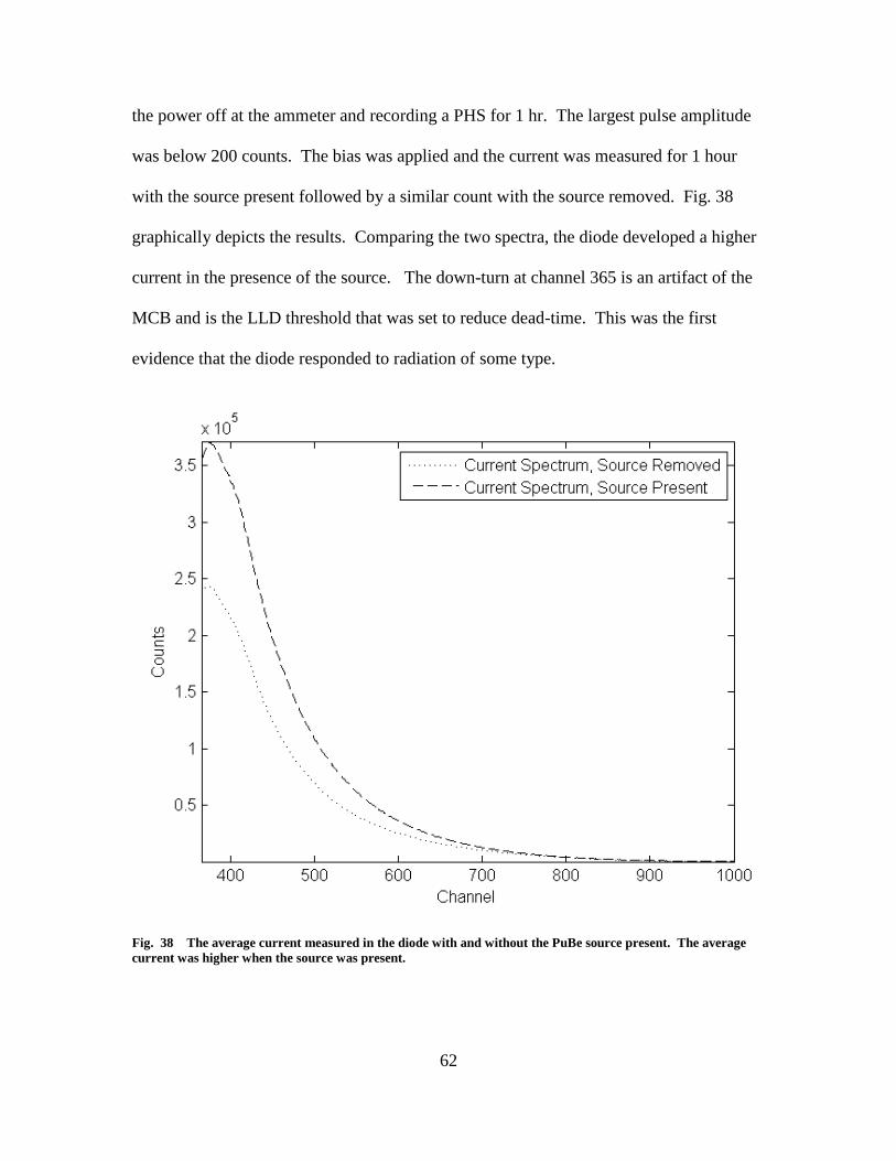
62
the power off at the ammeter and recording a PHS for 1 hr. The largest pulse amplitude
was below 200 counts. The bias was applied and the current was measured for 1 hour
with the source present followed by a similar count with the source removed. Fig. 38
graphically depicts the results. Comparing the two spectra, the diode developed a higher
current in the presence of the source. The down-turn at channel 365 is an artifact of the
MCB and is the LLD threshold that was set to reduce dead-time. This was the first
evidence that the diode responded to radiation of some type.
Fig. 38 The average current measured in the diode with and without the PuBe source present. The average
current was higher when the source was present.
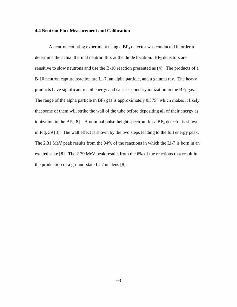
63
4.4 Neutron Flux Measurement and Calibration
A neutron counting experiment using a BF3 detector was conducted in order to
determine the actual thermal neutron flux at the diode location. BF3 detectors are
sensitive to slow neutrons and use the B-10 reaction presented as (4). The products of a
B-10 neutron capture reaction are Li-7, an alpha particle, and a gamma ray. The heavy
products have significant recoil energy and cause secondary ionization in the BF3 gas.
The range of the alpha particle in BF3 gas is approximately 0.375” which makes it likely
that some of them will strike the wall of the tube before depositing all of their energy as
ionization in the BF3 [8]. A nominal pulse-height spectrum for a BF3 detector is shown
in Fig. 39 [8]. The wall effect is shown by the two steps leading to the full energy peak.
The 2.31 MeV peak results from the 94% of the reactions in which the Li-7 is born in an
excited state [8]. The 2.79 MeV peak results from the 6% of the reactions that result in
the production of a ground-state Li-7 nucleus [8].
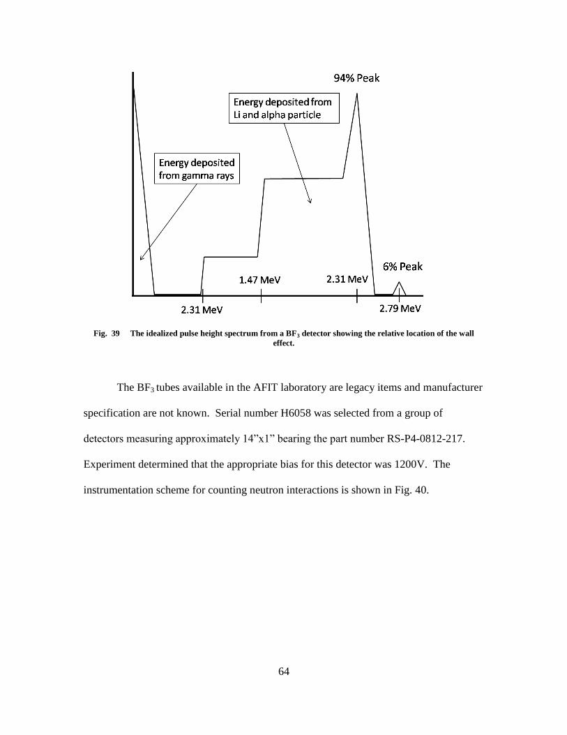
64
Fig. 39 The idealized pulse height spectrum from a BF3 detector showing the relative location of the wall
effect.
The BF3 tubes available in the AFIT laboratory are legacy items and manufacturer
specification are not known. Serial number H6058 was selected from a group of
detectors measuring approximately 14”x1” bearing the part number RS-P4-0812-217.
Experiment determined that the appropriate bias for this detector was 1200V. The
instrumentation scheme for counting neutron interactions is shown in Fig. 40.
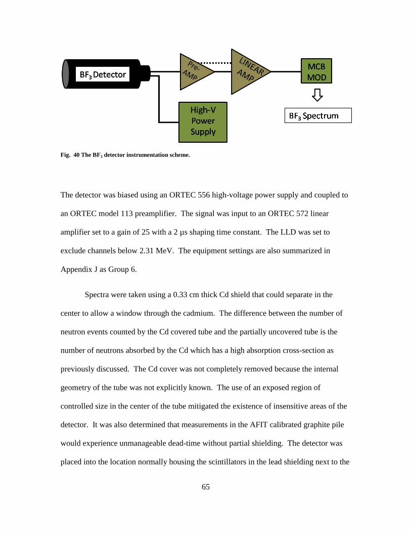
65
Fig. 40 The BF3 detector instrumentation scheme.
The detector was biased using an ORTEC 556 high-voltage power supply and coupled to
an ORTEC model 113 preamplifier. The signal was input to an ORTEC 572 linear
amplifier set to a gain of 25 with a 2 µs shaping time constant. The LLD was set to
exclude channels below 2.31 MeV. The equipment settings are also summarized in
Appendix J as Group 6.
Spectra were taken using a 0.33 cm thick Cd shield that could separate in the
center to allow a window through the cadmium. The difference between the number of
neutron events counted by the Cd covered tube and the partially uncovered tube is the
number of neutrons absorbed by the Cd which has a high absorption cross-section as
previously discussed. The Cd cover was not completely removed because the internal
geometry of the tube was not explicitly known. The use of an exposed region of
controlled size in the center of the tube mitigated the existence of insensitive areas of the
detector. It was also determined that measurements in the AFIT calibrated graphite pile
would experience unmanageable dead-time without partial shielding. The detector was
placed into the location normally housing the scintillators in the lead shielding next to the

66
howitzer. A spectrum was taken with the detector fully shielded and another with a 1”
separation between shield halves. The experiment was repeated to observe the effect on
the flux at the diode location when the PuBe was lowered from the beam position to the
storage position. Another experiment determined the count behind the howitzer at a point
in space analogous to the diode location but not in line-of-sight of the beam tube. The
detector was placed 5.25” away from the howitzer and 17” up from the floor, the analog
to the diode position. The detector was placed as depicted in Fig. 41.
Fig. 41 The positioning of the BF3 detector for a neutron flux measurement of the neutron howitzer. A
measurement was taken at the rear of the howitzer for a comparison to the beam tube side as depicted in „A‟.
The measurement at the diode location required the removal of the LaBr detectors so the BF3 tube could occupy
their location in the lead shielding shown in „B‟. The Cd cover over the BF3 tube could be separated to a precise
distance in order to make measurements of the covered and bare detector. „C‟ shows a close-up of the detector
with the Cd shield separated. The square aperture in the far ground has line-of-sight to the beam port.
A typical experimental pulse height spectrum is shown as Fig. 42. It is believed that the
old age of the detector was a contributing factor to the non-ideal spectrum. The sum of
the non-gamma ray induced counts was computed using the GammaVission Region of
Interest Tool [33]. This sum represents the total number of neutron interactions in the
counting period but does not provide information about the energy of the neutrons.

67
Fig. 42 An experimental pulse height spectrum taken with the BF3 detector. Shown are three sets of data from
a 1 hour count i) a 1” separation of the Cd cover ii) a completely covered detector, and iii) the difference
between i and ii. The sum of the counts under the Net Counts line represents the number of neutrons that were
absorbed by the Cd shielding.
Using some nominal parameters for BF3 detectors, the thermal neutron flux was
calculated for each data pair. The values used in this calculation are listed in Table VIII.
MATLAB® was used to compute the flux as described below and the code is included in
Appendix G [35].
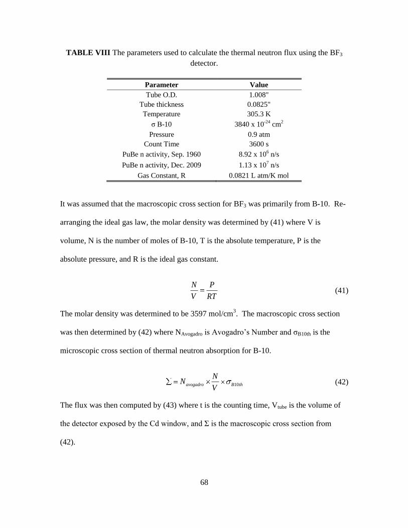
68
TABLE VIII The parameters used to calculate the thermal neutron flux using the BF3
detector.
Parameter Value
Tube O.D. 1.008"
Tube thickness 0.0825"
Temperature 305.3 K
σ B-10 3840 x 10-24
cm2
Pressure 0.9 atm
Count Time 3600 s
PuBe n activity, Sep. 1960 8.92 x 10⁶ n/s
PuBe n activity, Dec. 2009 1.13 x 10⁷ n/s
Gas Constant, R 0.0821 L atm/K mol
It was assumed that the macroscopic cross section for BF3 was primarily from B-10. Re-
arranging the ideal gas law, the molar density was determined by (41) where V is
volume, N is the number of moles of B-10, T is the absolute temperature, P is the
absolute pressure, and R is the ideal gas constant.
N P
V RT (41)
The molar density was determined to be 3597 mol/cm3. The macroscopic cross section
was then determined by (42) where NAvogadro is Avogadro‟s Number and σB10th is the
microscopic cross section of thermal neutron absorption for B-10.
10avogadro B th
NN
V (42)
The flux was then computed by (43) where t is the counting time, Vtube is the volume of
the detector exposed by the Cd window, and Σ is the macroscopic cross section from
(42).
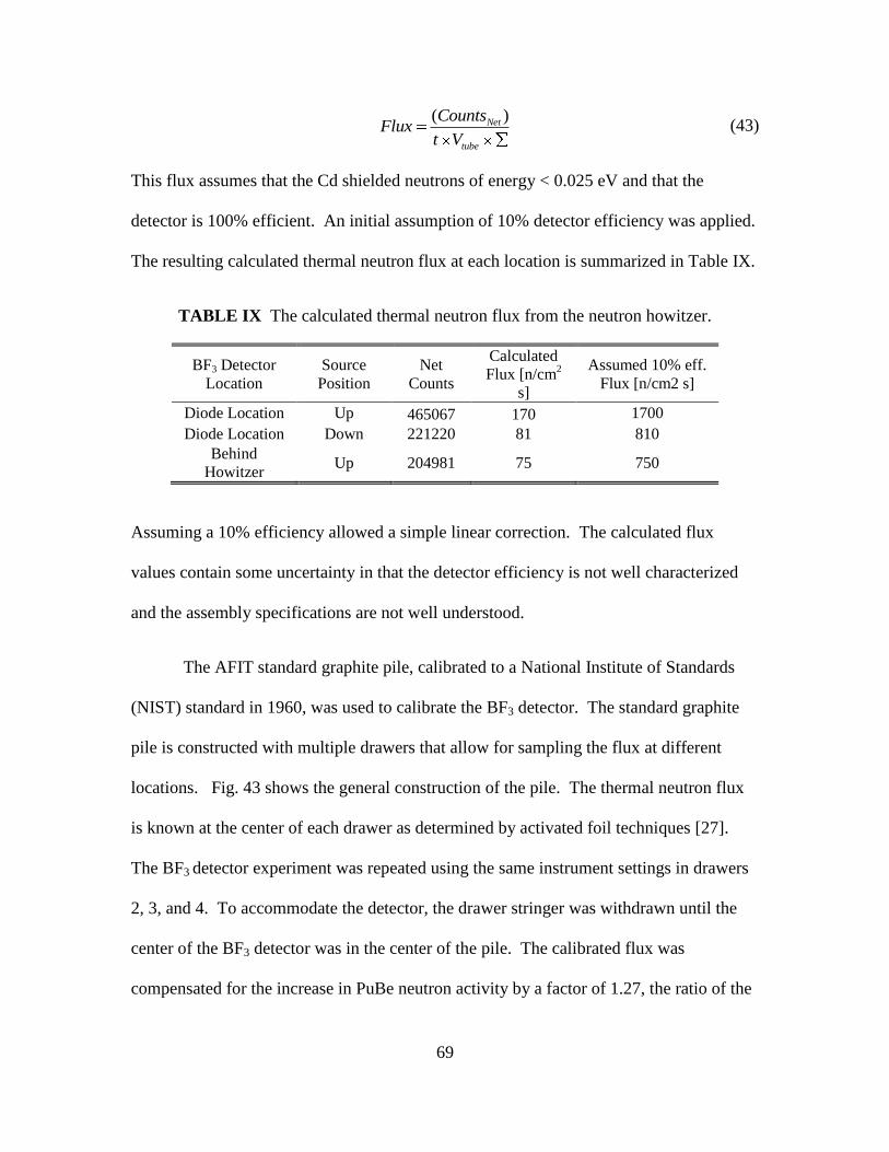
69
( )Net
tube
CountsFlux
t V (43)
This flux assumes that the Cd shielded neutrons of energy < 0.025 eV and that the
detector is 100% efficient. An initial assumption of 10% detector efficiency was applied.
The resulting calculated thermal neutron flux at each location is summarized in Table IX.
TABLE IX The calculated thermal neutron flux from the neutron howitzer.
BF3 Detector
Location Source
Position Net
Counts
Calculated
Flux [n/cm2
s]
Assumed 10% eff.
Flux [n/cm2 s]
Diode Location Up 465067 170 1700
Diode Location Down 221220 81 810 Behind
Howitzer Up 204981 75 750
Assuming a 10% efficiency allowed a simple linear correction. The calculated flux
values contain some uncertainty in that the detector efficiency is not well characterized
and the assembly specifications are not well understood.
The AFIT standard graphite pile, calibrated to a National Institute of Standards
(NIST) standard in 1960, was used to calibrate the BF3 detector. The standard graphite
pile is constructed with multiple drawers that allow for sampling the flux at different
locations. Fig. 43 shows the general construction of the pile. The thermal neutron flux
is known at the center of each drawer as determined by activated foil techniques [27].
The BF3 detector experiment was repeated using the same instrument settings in drawers
2, 3, and 4. To accommodate the detector, the drawer stringer was withdrawn until the
center of the BF3 detector was in the center of the pile. The calibrated flux was
compensated for the increase in PuBe neutron activity by a factor of 1.27, the ratio of the
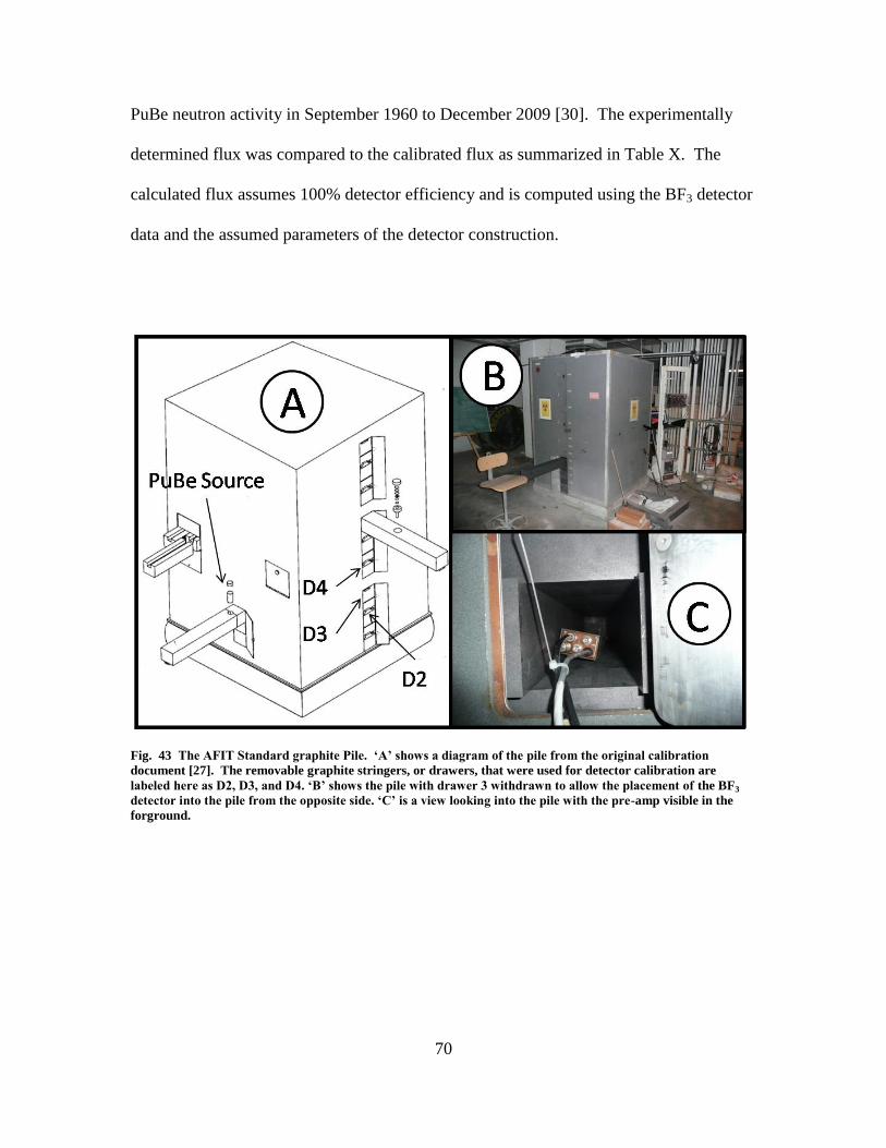
70
PuBe neutron activity in September 1960 to December 2009 [30]. The experimentally
determined flux was compared to the calibrated flux as summarized in Table X. The
calculated flux assumes 100% detector efficiency and is computed using the BF3 detector
data and the assumed parameters of the detector construction.
Fig. 43 The AFIT Standard graphite Pile. „A‟ shows a diagram of the pile from the original calibration
document [27]. The removable graphite stringers, or drawers, that were used for detector calibration are
labeled here as D2, D3, and D4. „B‟ shows the pile with drawer 3 withdrawn to allow the placement of the BF3
detector into the pile from the opposite side. „C‟ is a view looking into the pile with the pre-amp visible in the
forground.

71
TABLE X A summary of the calculated and calibrated thermal neutron flux in the AFIT
standard graphite pile by drawer position.
BF3 Detector
Location Net
Counts Calculated
Flux [n/cm2 s]
Calibrated Flux
(compensated)
[n/cm2 s]
Calculated /
Calibrated
Drawer 2 47519100 17378 8839 1.97 Drawer 3 60250919 22034 10117 2.18
Drawer 4 54478284 19923 7307 2.73
It was determined that the computed thermal neutron flux was a factor of 2-3 times the
calibrated flux. The disparity between the calibrated and computed values is most likely
due to the Cd shield thickness which determined the energy of the neutrons it absorbed.
Modeling the problem as a thin neutron beam moving through the Cd into the detector,
the attenuation equation can be used to compare the intensity of the transmitted beam, I,
to the intensity of the incident beam, I0. The mass attenuation coefficient is energy
dependent and represented by µ. The density of the Cd is given by ρ. Rearranging (44)
to (45) and plotting the cross-section dependent, and thus energy dependent, ratio of
incident intensity to the output intensity for 0.33 cm Cd results in Fig. 44.
0
x
I I e (44)
0
( , )xI
E eI
(45)
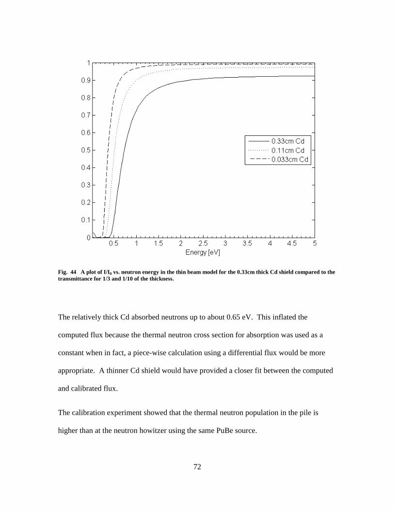
72
Fig. 44 A plot of I/I0 vs. neutron energy in the thin beam model for the 0.33cm thick Cd shield compared to the
transmittance for 1/3 and 1/10 of the thickness.
The relatively thick Cd absorbed neutrons up to about 0.65 eV. This inflated the
computed flux because the thermal neutron cross section for absorption was used as a
constant when in fact, a piece-wise calculation using a differential flux would be more
appropriate. A thinner Cd shield would have provided a closer fit between the computed
and calibrated flux.
The calibration experiment showed that the thermal neutron population in the pile is
higher than at the neutron howitzer using the same PuBe source.
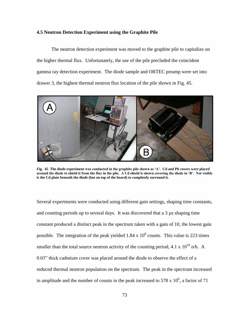
73
4.5 Neutron Detection Experiment using the Graphite Pile
The neutron detection experiment was moved to the graphite pile to capitalize on
the higher thermal flux. Unfortunately, the use of the pile precluded the coincident
gamma ray detection experiment. The diode sample and ORTEC preamp were set into
drawer 3, the highest thermal neutron flux location of the pile shown in Fig. 45.
Fig. 45 The diode experiment was conducted in the graphite pile shown as „A‟. Cd and Pb covers were placed
around the diode to shield it from the flux in the pile. A Cd shield is shown covering the diode in „B‟. Not visible
is the Cd plate beneath the diode (but on top of the board) to completely surround it.
Several experiments were conducted using different gain settings, shaping time constants,
and counting periods up to several days. It was discovered that a 3 µs shaping time
constant produced a distinct peak in the spectrum taken with a gain of 10, the lowest gain
possible. The integration of the peak yielded 1.84 x 10⁸ counts. This value is 223 times
smaller than the total source neutron activity of the counting period, 4.1 x 10¹⁰
n/h. A
0.03” thick cadmium cover was placed around the diode to observe the effect of a
reduced thermal neutron population on the spectrum. The peak in the spectrum increased
in amplitude and the number of counts in the peak increased to 578 x 106, a factor of 71
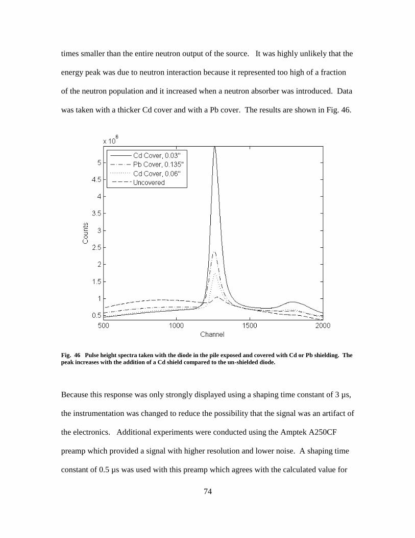
74
times smaller than the entire neutron output of the source. It was highly unlikely that the
energy peak was due to neutron interaction because it represented too high of a fraction
of the neutron population and it increased when a neutron absorber was introduced. Data
was taken with a thicker Cd cover and with a Pb cover. The results are shown in Fig. 46.
Fig. 46 Pulse height spectra taken with the diode in the pile exposed and covered with Cd or Pb shielding. The
peak increases with the addition of a Cd shield compared to the un-shielded diode.
Because this response was only strongly displayed using a shaping time constant of 3 µs,
the instrumentation was changed to reduce the possibility that the signal was an artifact of
the electronics. Additional experiments were conducted using the Amptek A250CF
preamp which provided a signal with higher resolution and lower noise. A shaping time
constant of 0.5 µs was used with this preamp which agrees with the calculated value for

75
charge collection time in the diode using (38). The result was generally similar, but the
single pronounced peak in the previous experiment was found to be two peaks as shown
in Fig. 47.
Fig. 47 Pulse height spectra from the diode in the pile coupled to the Amptek preamp. The spectra are of
higher resolution than with the ORTEC preamp and show two energy peaks.
The experiment was modeled using MCNP5 in order to determine the differential
neutron flux at the diode with and without the Cd covering. The code can be found in
Appendix E. Fig. 48 shows the geometry of the model and the results. The Cd shielding
decreased the thermal neutron population as expected. The total number of neutrons that
the diode could detect depends on the point at which the reaction no longer occurs, i.e.
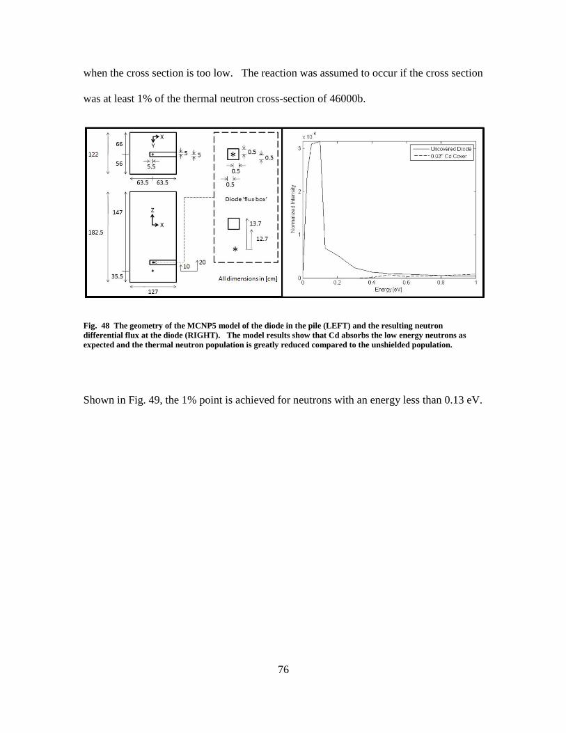
76
when the cross section is too low. The reaction was assumed to occur if the cross section
was at least 1% of the thermal neutron cross-section of 46000b.
Fig. 48 The geometry of the MCNP5 model of the diode in the pile (LEFT) and the resulting neutron
differential flux at the diode (RIGHT). The model results show that Cd absorbs the low energy neutrons as
expected and the thermal neutron population is greatly reduced compared to the unshielded population.
Shown in Fig. 49, the 1% point is achieved for neutrons with an energy less than 0.13 eV.

77
Fig. 49 The total neutron cross-section for naturally abundant Gd. The cross-section is greater than 1% of
46000 b, the thermal energy cross section, for all energies greater than 0.13 eV.
Using the results of the MCNP5 model, the probability per source neutron (PPSN)
for energies up to 0.13 eV is 9.349 × 10⁻⁴
in a 1 cm3 volume. PPSN is the output of the
energy tally from the MCNP model and is the probability of a single source neutron
populating a specified energy bin in the tally. Multiplying the PPSN by the current
neutron activity of 1.14 × 10⁷n/s, the 3600s counting period, and the active volume of the
diode yields a total of 8.49 × 10⁵ neutrons that could be detected by the diode. Assuming
100% diode efficiency, this value is still 3 orders of magnitude below the integrated
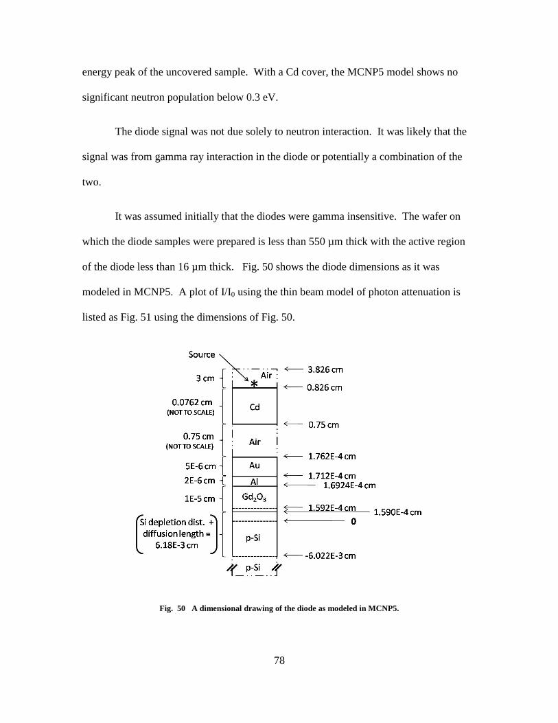
78
energy peak of the uncovered sample. With a Cd cover, the MCNP5 model shows no
significant neutron population below 0.3 eV.
The diode signal was not due solely to neutron interaction. It was likely that the
signal was from gamma ray interaction in the diode or potentially a combination of the
two.
It was assumed initially that the diodes were gamma insensitive. The wafer on
which the diode samples were prepared is less than 550 µm thick with the active region
of the diode less than 16 µm thick. Fig. 50 shows the diode dimensions as it was
modeled in MCNP5. A plot of I/I0 using the thin beam model of photon attenuation is
listed as Fig. 51 using the dimensions of Fig. 50.
Fig. 50 A dimensional drawing of the diode as modeled in MCNP5.

79
If the active region of the diode is only the depletion region, the device is insensitive to
photons with energies greater than 3 keV as shown in Fig. 51. If the charge, however, is
collected over a greater distance such as the sum of the depletion and diffusion length in
the Si, then the device is sensitive to photons up to 8 keV, also shown in Fig. 51. Low
energy gamma rays could potentially deposit energy in the diode. If the Cd cover down-
scattered the gamma spectrum, it would provide an explanation for the larger feature.
An experiment was conducted to measure the gamma spectrum at the diode location in
the pile using a LaBr scintillator. Lead and cadmium covers of the same thickness as
used on the diode were constructed to cover the scintillator.
Fig. 51 A comparison if initial and final photon intensity in the narrow beam model for different thicknesses of
Si in various regios of the diode. The initial photon intensity is I0, the final intensity is I. The thicker the Si, the
lower the value of I/I0 which implies insensitivity at that energy. The thicknesses used are 550 x 10-4, 6.18 x 10⁻³,
and 1.59 x 10⁻⁴ cm corresponding to the wafer thickness, depletion plus diffusion length, and the depletion
length. The spike in I/I0 is due to a K shell energy level at 1.83 keV.
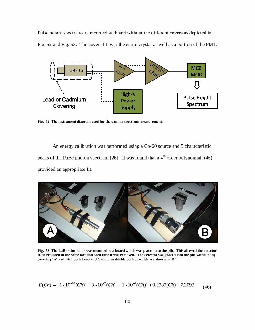
80
Pulse height spectra were recorded with and without the different covers as depicted in
Fig. 52 and Fig. 53. The covers fit over the entire crystal as well as a portion of the PMT.
Fig. 52 The instrument diagram used for the gamma spectrum measurement.
An energy calibration was performed using a Co-60 source and 5 characteristic
peaks of the PuBe photon spectrum [26]. It was found that a 4th
order polynomial, (46),
provided an appropriate fit.
Fig. 53 The LaBr scintillator was mounted to a board which was placed into the pile. This allowed the detector
to be replaced in the same location each time it was removed. The detector was placed into the pile without any
covering „A‟ and with both Lead and Cadmium shields both of which are shown in „B‟.
10 4 7 3 4 2( ) 1 10 ( ) 3 10 ( ) 1 10 ( ) 0.2787( ) 7.2093E Ch Ch Ch Ch Ch (46)

81
The results, depicted graphically in Fig. 54, show that the shielding materials did soften
the gamma ray spectrum. Since lower energy photons have a higher probability of
interaction, this provides a reason for the experimental result but only in the energy
region below 20 keV. Lead was observed to significantly down-scatter the spectrum and
provide a dominant peak centered around 36 keV. Since this feature was not strongly
observed in the diode spectrum, it is probable that photons of this higher energy are less
likely to interact in the diode.
Fig. 54 Pulse height spectra data taken with a LaBr detector inside the graphite pile at the diode location. The
presence of shielding material softens the spectra.

82
A quantitative link between the diode response and the photon spectra was developed
using a simple absorbance model. Fig. 55 depicts the observed diode spectrum peaks
with the corresponding gamma ray peaks for the same shield configurations.
Fig. 55 The PHS from the diode (left) and the PHS from the LaBr detector (right). The arrows show the
relationship between the diode response and the gamma ray energy that produced it.
The diode peak centroids are nearly at the same energy because only those electrons
liberated in the sensitive diode region are collected as a pulse. A photon that continues to
deposit energy as ionization beyond the diffusion length of an electron does not
contribute further to the signal. Thus, within a narrow range of photon energies, all
photons deposit nearly the same energy in the diode. The amplitude of the diode
response increased with the number of photons that interacted. Less energetic photons
are more likely to interact than those of high energy. Qualitatively, the Cd shielding
produced a number of 15 keV photons which were more likely to interact in the diode
than the greater number of 36 keV photons produced by the Pb shielding.

83
Integrating the spectral peaks from both detectors and applying the calculated absorbance
to the LaBr peaks quantitatively corroborates the relationship. The energy dependent
absorbance fraction can be calculated using (47). The ratio of photons absorbed to
photons incident, or absorbance fraction, is represented by Ia/Io. The mass energy
absorption coefficient is represented by µen. The material density is ρ and the thickness
of the absorbing material is t.
( )
1en t
a
o
Ie
I (47)
The absorbance fraction for 60µm of Si was computed at the energies corresponding to
the centroids of the photon spectra experimentally determined using the LaBr detector.
Table XI summarizes the result of the calculation.
TABLE XI The computed absorbance fraction of gamma rays in silicon.
Energy [keV] µen/ρ [cm2/g] Ia/Io
15 9.79 0.128 22 3.49 0.048
36 0.750 0.010
ρ Si = 2.33 g/cm3, thickness Si = 60 µm
A plot of the integrated peaks against their centroid energies for both the diode and
scintillator spectra is shown as Fig. 56. The diode peaks were recorded at nearly identical
energies but the integrated diode peaks (plotted as squares) are displayed at the energy of
the most probable photon energy using the relations shown in Fig. 55.

84
Fig. 56 The diode response explained by the energy deposition by gamma ray photons.
The total number of counts under the peaks at the centroid peak energies of the LaBr
spectra are plotted as circles. The peak at 15 keV was observed, or produced by, the
presence of the Cd shield. The peak at 36 keV was observed when the Pb shield was
used. The 22 keV peak was observed when the diode was un-shielded. Multiplying the
absorbance fractions at each energy to the LaBr peaks scales the peaks for absorbance
probability. This is plotted as triangles. The integrated diode peaks exhibit the same
relative relationship as the absorption adjusted LaBr peaks. This is more clearly shown
when the absorption adjusted LaBr peaks are scaled by 1000 and plotted as diamonds

85
which nearly overlap the diode peaks. This provides more evidence that the diode was
responding to gamma rays.
MCNP5 was used to model the energy deposited in the diode from the PuBe
gamma spectrum with and without the Cd shielding. The MCNP5 input files are in
Appendix I. Fig. 57 depicts the modeled PuBe gamma spectrum and Fig. 58 graphically
depicts the energy deposition in the modeled diode from the gamma spectrum.
Fig. 57 The photon energy spectrum of the PuBe source used for MCNP simulation. The spectrum was
developed from published data taken with a high-purity Germanium detector [26].
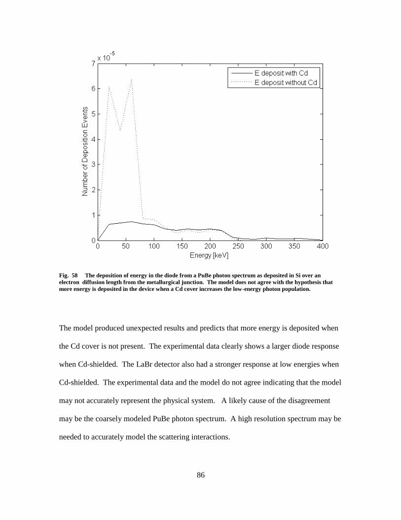
86
Fig. 58 The deposition of energy in the diode from a PuBe photon spectrum as deposited in Si over an
electron diffusion length from the metallurgical junction. The model does not agree with the hypothesis that
more energy is deposited in the device when a Cd cover increases the low-energy photon population.
The model produced unexpected results and predicts that more energy is deposited when
the Cd cover is not present. The experimental data clearly shows a larger diode response
when Cd-shielded. The LaBr detector also had a stronger response at low energies when
Cd-shielded. The experimental data and the model do not agree indicating that the model
may not accurately represent the physical system. A likely cause of the disagreement
may be the coarsely modeled PuBe photon spectrum. A high resolution spectrum may be
needed to accurately model the scattering interactions.
87
It was concluded that the diode produced a signal in response to the gamma ray
fluence. It is possible that an indistinguishable neutron signal was present but this could
not be confirmed.
4.6 Sr-90 Experiment
The mechanism by which the neutron capture produces a signal in the diode is the
ionization of atoms in the material by internal conversion electrons. This process
liberates electrons which then are collected as charge in the active diode region. An
experiment was conducted using a Strontium-90 source as an external supply of electrons
in order to verify that the charge collection process of the diode functioned. Sr-90 has a
half life of 28.79 years and decays by emission of a beta particle. It is a pure beta emitter
with an end point energy of 546 keV providing an average particle energy of 195.8 keV
[28]. The daughter product is Yttrium-90 which has a half-life of 64.1 hours. Y-90
decays through beta emission with an end point energy of 2280.1 keV providing an
average particle of 933.7 keV for 99.9885% of decays [28]. It also emits a less intense
beta particle with an end point energy of 519.4 keV which has an average energy of 185.6
keV for 0.0115% of decays. The Y-90 nucleus decays to a stable Zr-90 nucleus [28].
Fig. 59 graphically depicts the decay of both Sr-90 and Y-90.

88
Fig. 59 The decay schemes for Sr-90 and Y-90.
The Sr-90 source was produced originally as a medical device in 1951. This
legacy source has not been fully characterized for laboratory use. The activity and
containment geometry of the Sr-90 are not precisely known. Table XII summarizes the
parameters of the source used for calculation [29].
TABLE XII The parameters of AFIT source number 00365, the Sr-90 eye applicator.
Parameter Value
Manufacturer Tracerlab Initial Activity, 28 Feb. 1951 25mCi
Activity in Dec. 2009 6mCi
Active Source Diameter 5mm
Source Containment Dia. 12.7mm
Protective Shield Diameter 4 inch Protective Shield Thickness 3/8 inch Overall Length of Assembly 6.75 inch
Aluminum Source 'Window' 10 mils
S. Steel Source 'Window' 2 mils
Because the beta particle shares its energy with the anti-neutrino, the emitted beta
energies follow a distribution out to the maximum, or end point energy. This distribution
can be represented by (48) where Te is the kinetic energy of the beta particle, me is the
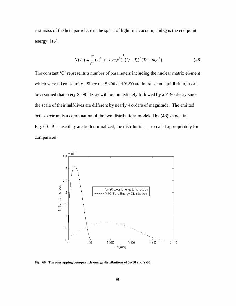
89
rest mass of the beta particle, c is the speed of light in a vacuum, and Q is the end point
energy [15].
1
2 2 2 225
( ) ( 2 ) ( ) ( )e e e e e e
CN T T T m c Q T Te m c
c (48)
The constant „C‟ represents a number of parameters including the nuclear matrix element
which were taken as unity. Since the Sr-90 and Y-90 are in transient equilibrium, it can
be assumed that every Sr-90 decay will be immediately followed by a Y-90 decay since
the scale of their half-lives are different by nearly 4 orders of magnitude. The emitted
beta spectrum is a combination of the two distributions modeled by (48) shown in
Fig. 60. Because they are both normalized, the distributions are scaled appropriately for
comparison.
Fig. 60 The overlapping beta-particle energy distributions of Sr-90 and Y-90.

90
The source is housed in a stainless steel and aluminum body as pictured in
Fig. 61. The beta particles that provide a signal must escape the source housing, pass
through the air, the inactive layers of the diode, and finally interact in the active region.
For the average beta energies of 195.8 and 933.7 keV, the linear stopping power
approximation shows that a large fraction of the beta particles do not escape the source
housing. Table XIII summarizes the stopping power data.
Fig. 61 The Sr-90 source was originally produced as a medical applicator shown in „A‟. The source, pictured in
„B‟ has a plastic shield that slides up and down the shaft which is designed to shield the operator from radiation.
The source is sitting head-down and is covered by a thick aluminum shield for storage which is removed for use.
The Sr-90 is enclosed in a stainless steel and aluminum element on the end of the applicator rod.

91
TABLE XIII The linear stopping power of the Sr-90 source housing.
Stainless Steel Aluminum
Thickness [cm] 0.00508 0.0254
ρ [g/cm3] 8 2.7
Stopping Power for 195.8 keV [keV
cm2/g] 1947 2183
Stopping power for 933.7 keV [keV
cm2/g] 1354 1492
Energy absorbed at 195.8 keV [keV] 79 150
Total [keV] 229
Energy absorbed at 933.7 keV [keV] 55 102
Total [keV] 157
Table XIII shows that nearly all of the particles emitted by Sr-90 are contained
within the source housing since energies up to 229 keV will be stopped by a combination
of the steel and aluminum „window‟ of the housing. A fraction of the Y-90 beta particles
will also be stopped. The stopping power is energy dependent. The threshold of particle
absorption listed in Table XII is based upon the average particle energy. A multi-group
approach would produce a better approximation for the escaping beta particle energies.
The energy distribution of the emitted beta particles is shown in Fig. 62. The source beta
particle distribution is nearly all from Y-90, a statement corroborated by others using
similar sources [29]. Appendix H contains the MATLAB® code to calculate the fraction
of emitted beta particles from each nuclide. Only 0.2 % of the Sr-90 emissions are
passed through the source windows while 82.3% of the Y-90 particles escape.

92
Fig. 62 The energy distribution of the beta particles emitted from the source.
The energy distribution is further altered by the interaction of the air and finally in the
gold and aluminum which constitutes the contacts sputtered over the gadolina layer of the
diode. After adjusting the distribution for these material interactions and multiplying it
by source activity, it was integrated and subsequently divided by the spherical area
provided by the source to diode distance as depicted in Fig. 63.

93
Fig. 63 A diagram of the Sr-90 experiment. Pictured inside aluminum shielding „4‟, are the diode and signal
wires „2‟, the source „1‟, the concrete floor „3‟, and the source and sample stand „5‟.
The diode was placed at 0.75” and 1.375” from the source. The flux was calculated to be
1.2 × 10⁷ and 3.57 × 10
6 β/cm
2 s respectively. With the diode under bias using the same
parameters as used in the graphite pile, pulse height spectra data was taken at each
distance as well as a background when the source was removed from the laboratory. The
result is shown graphically as Fig. 64. Subtracting the background and integrating
provided 1.00 × 10⁸ counts at 0.75” and 21.52× 10
6 counts at 1.375”. The counting
period was 3600 seconds. The diode sample contained 5 diodes each with approximately
8.14× 10⁻¹²
cm2 of surface area. The number of beta particle interactions that could be
expected at 0.75” should be 1.75 × 10¹⁰
and at 1.375”, 5.23 × 10⁹. Using these values, it
was found that the diode efficiency for beta particles was 0.005 at 0.75”, and 0.0041 at
1.375”. Stated another way, the diodes only detected about 0.5 % of the beta particles.
The low efficiency is partly due to the 2.001V low level discriminator setting used with
the multi-channel buffer. This removed a large fraction of the diode signal but was used

94
to reduce dead time. Since the low energy channels of the spectrum contain the bulk of
the counts as shown in Fig. 64, the actual efficiency may be greater by an order of
magnitude or more. Qualitatively, the diode response followed the expectation of a
higher signal with a higher flux close to the source and a weaker signal with a lower flux
farther from the source.
Fig. 64 The pulse height spectrum taken with the diode exposed to a beta source. The diode response was
higher closer to the source.
The Sr-90 experiment provided evidence that electrons in the active region of the
diode can produce a signal. The total number of gamma rays from the Y-90 decay that
could have interacted with the diode was 6.5 × 10⁴ at 0.75” and 1.9 × 10
4 at 1.375”. This

95
small fraction of the source emissions does not account for the number of events recorded
in the PHS. Although the diode is gamma sensitive, this experiment clearly showed that
the response was due to the beta particle flux. The experiment does not, however, show
the diode response to beta particles at the target energy of 79 keV. The Sr-90 source did
not emit beta particles below 200 keV. Only a small fraction of down-scattered beta
particles in this energy range would have interacted with the diode.
4.7 Cesium-137 Experiment
A 1.2 Ci Cs-137 source was used to find the diode response to a hard gamma flux.
Cs-137 decays to barium-137 with a half-life of 30.04 years. 94.4% of the decays
produce a beta particle with an average energy of 174.3 keV and an end point energy of
514 keV [28]. Beta emission is followed immediately by a gamma emission of
661.657 keV. Fig. 65 graphically depicts the decay process.
Fig. 65 The decay of Cs-137 to Ba-137.
The precise source activity during the experiment was 2.92 × 10¹⁰
Bq. The diode
was placed 1.608” from the Cs-137 source as shown in Fig. 66. The solid angle was

96
0.00194 steradians as determined by using the total diode area for 5 active diodes at the
stated distance. For a count duration of 6800 seconds, the number of 661.657 keV
gamma rays impinging on the diode is 3.63 × 10¹¹
. There is a fraction of beta particles as
well with a maximum number of 2 × 10¹⁰
. The encapsulation of the Cs-137 comprises 3
layers of stainless steel totaling 0.12” of shielding. The fraction of beta particles emitted
is near zero. The integration of the experimental pulse height spectrum of Fig. 67
yielded 1.2617 × 10⁸ counts over a 6800 second period. The gamma efficiency computes
to 0.035%.
The high dead-time experienced during measurement necessitated setting the
LLD to 0.996 V in the MCB. This removed the energy events in the first 199 channels.
Since the lower channels contain most of the counts, this is likely a contributor to the low
efficiency of detection. However, it is likely that most of the gamma rays passed
completely through the sample without interaction. Scattering of the spectrum by the
containment vessel around the source as well as the sample itself may also have softened
the spectrum.
The pronounced energy features observed in response to the PuBe source were
not observed with the nearly mono-energetic 662 keV gamma ray source. It is possible to
conclude that the diode is reasonably insensitive to gamma rays of 662 keV.
The original purpose of the Cs-137 experiment was to provide a diode response
using instrument settings identical to an experiment conducted in the graphite pile.
Because the PuBe source and Cs-137 have activities on the order of a Ci, the goal was to
determine the contribution of the gamma spectrum to the total diode response. An

97
amplification shaping time constant of 0.5 µs was used and not the 3 µs constant found to
be optimal for the ORTEC preamp.
Fig. 66 The Cs-137 source belonged to AFFRAD and is used for calibrating instrumentation. The source is
stored inside a containment vessel located at the end of a movable stand shown in „A‟. The diode was placed
1.608” away from the exposed source. This distance was achieved by placing the diode inside the line-of-sight
port of the pig as shown in „B‟ and „C‟. Close placement maximized the gamma flux.
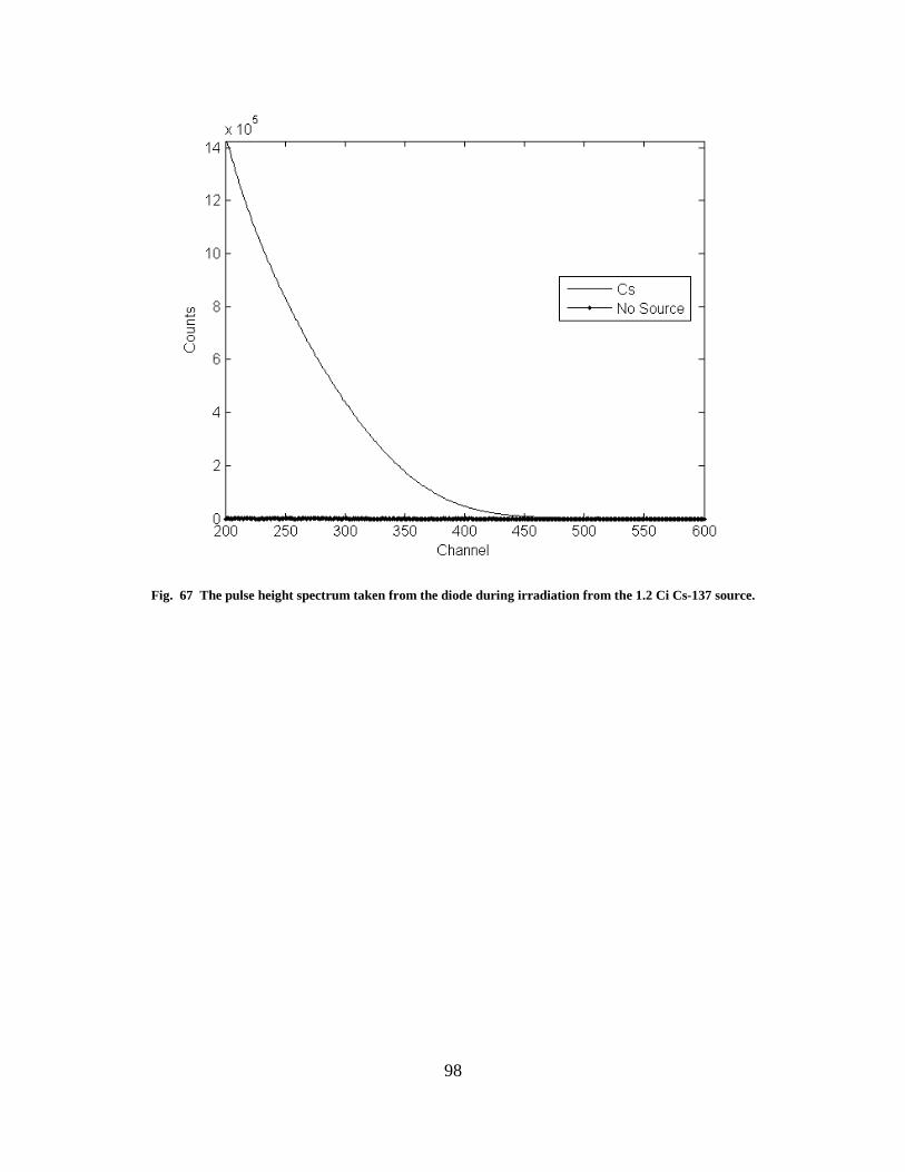
98
Fig. 67 The pulse height spectrum taken from the diode during irradiation from the 1.2 Ci Cs-137 source.
99
V. CONCLUSIONS
5.1 Conclusions
No direct evidence of neutron detection was observed during the course of
experimentation. Under the experimental conditions, neutron interactions undoubtedly
occurred in the diode. However, the presence of a relatively high leakage current and the
gamma ray sensitivity of the novel diode produced a signal that may have masked the
presence of neutron interaction.
Experimentation supports the following statements:
1. The best diodes prepared using the supercritical water deposition process have leakage
currents on the order of tens of micro-Amps at a reverse bias of 1 volt. A typical
commercially manufactured diode has a leakage current of pico-amps. The novel diodes
are relatively leaky.
2. The diode is capable of collecting charge from ionization produced by energetic
electrons in the active region. This was observed as the diode response to the Sr-90 beta
particle flux.
3. The diodes are sensitive to low energy gamma rays. It is likely that the energy region
in which this was observed was between 10 and 20 keV.

100
It is not possible to make a complete determination as to the feasibility of a
Gd2O3/Si diode for neutron detection based on the experimental data. As the process for
diode fabrication improves and devices with lower leakage currents become available, the
potential as a neutron detector increases. However, the discovery that the diode is
gamma sensitive is problematic for neutron detection unless a way is found, by
spectroscopy or design, to specifically measure the conversion electron energy.
5.2 Recommendations for future work
5.2.1 Investigate the photon sensitivity.
It was determined that the diode was gamma sensitive. The diverse photon
spectrum of the PuBe source is not optimum for determining the specific energy range
over which the diode is sensitive. The use of multiple, mono-energetic gamma ray
sources would provide a means to determine specific sensitivity. A high-order response
to specific energies may yield information as to the region of the diode where the charge
is being collected. The double-peak feature of the diode response to low energy gamma-
rays may be caused by energy deposition in multiple regions of the diode with differing
mobilities.
5.2.2 Calibrate the diode spectrum.
The diode signal is uncalibrated. The resulting PHS may or may not include the
region of energies in the 79 keV range. A diode response to several energies of

101
monoenergetic electrons will determine the optimal instrumentation settings for neutron
pulse detection.
5.2.3 Diode modeling.
A more rigorous model of the diode using DaVinci® or similar semi-conductor
device modeling software package can be produced to determine the character of the
heterojunction [36]. It is possible that the active region of the diode is completely infused
with Gd2O3 due to the high-energy deposition process which would change the depletion
characteristics. The diode is currently modeled as an abrupt heterojunction which may
not be accurate.
A more rigorous MCNP modeling effort for gamma ray energy deposition may
provide the range of energy sensitivity and support an engineered solution to detecting
neutrons. Enhanced modeling may provide insight into where the energy is deposited in
the Gd / Si system.

102
APPENDICES

103
Appendix A: Diode Active Volume and Coincident Counting Time
Variables
Gd2O3 7.41 g cm3 ;
Si 2.33 g cm3 ;
AvogadroNum 6.02*^23;
MolWtGd2O3 352 g mole Gd2O3 ;
q 1.602*^-19 C ;
VbuiltIn 0.15 V ;
Vapplied 1.5 V ;
NA 5*^19 1 cm3 ;
ND 1*^15 1 cm3 ;
kGd2O3 17;
kSi 11.9;
not 8.85*^-14 F cm ;
46000*^-24 cm^2 ;
ContactDiameternm 814000 nm ;
ContactDiametercm 814000*^-7 cm ;
500 thermal neutrons cm2 s ;
LaBrCrystalDiam 0.18 cm, measured ;
StandOffClose 0.1 cm ;
StandOffFar .75 cm ;
CountGoal 100 neutron capture count goal ;
Calculate the Depletion Width, W, as an abrupt Heterojunction
Assuming Xp 0 && Xn 0, Solve Xp NA q Xn ND q,NA q Xp2
2 kSi not
Xn2 ND q
2 kGd2O3 notVbuiltIn Vapplied ,
Xp, Xn
Xp 3.18471 109, Xn 0.000159236 , Xp 3.18471 10
9, Xn 0.000159236
! Must update this from the above calculation !
Xp : 3.184714562745104`*^-9 ; Xn : 0.0001592357281372552`;
Wcm Xp Xn depletion width in cm
0.000159239
Wnm 10000000 Wcm depletion width in nm
1592.39
Calculate Active Gd nucleus density
NactiveGdAvogadroNum Gd2O3
MolWtGd2O3
2
1Gd atoms cm3
2.53456 1022
BigSigma NactiveGd macroscopic x section, 1 cm
1165.9
ActiveGdVolumeContactDiametercm ^2
4Xn cm3 5 all 5 diodes at once
4.14333 106
Number of Gd nuclei present in the Active Gd Volume
AbsNactiveGd NactiveGd ActiveGdVolume
1.05015 1017
104
Number of thermal neutron reactions in the device per second
NumThermNeutperSec AbsNactiveGd n cm2 s cm2 s
2.41534
Number of thermal neutron reactions in the device /s with coincident gamma 1107.6 keV
NumThermNeutperSecCoinc NumThermNeutperSec 0.113 0.136 0.3 0.5 s
0.00556785
Calculate LaBr geometric efficiency (One crystal is closer than the other due to the sample preparation)
ThetaClose ArcTan LaBrCrystalDiam 2 StandOffClose
0.732815
ThetaFar ArcTan LaBrCrystalDiam 2 StandOffFar
0.119429
OhmegaClose 2 1 Cos ThetaClose
1.61293
OhmegaFar 2 1 Cos ThetaFar
0.0447561
GeometricFraction OhmegaClose OhmegaFar 4
0.131915
Calculate Isotropic IC electron loss
IsoICelectronLoss 0.25; qualitative estimate of what occurs w o full deposit
Counting time to obtain significant results:
CountEventperS NumThermNeutperSecCoinc GeometricFraction IsoICelectronLoss s
0.00018362
TimeSecCountGoal
CountEventperS
544 603.
TimeHr TimeSec 3600
151.279
TimeDays TimeHr 24
6.30327

105
Appendix B: SNM Spontaneous Neutron Emission Rate Calculation
Pu239BR 3 10^ 12; 100
Pu240BR 5.7 10^ 8; 100
Pu241BR 2 10^ 14; 100
Pu239HL 24 110; Y
Pu240HL 6564; Y
Pu241HL 14.35; Y
U235BR 7 10^ 9; 100
U238BR 0.0000005; 100
U238HL 4.468 10^9; Y
U235HL 703 800 000; Y
PuNperDecay 2.89;
UNperDecay 2.44;
PUInitialAmount 100.; 1.; 1 gram
UInitialAmount 100.; 1 gram
NA 6.02 10^23;
YperS 1 31 536 000; year second
ActivityPU239 Log 2 Pu239HL PUInitialAmount NA 239 YperS; decays per second for PU239
ActivityPU240 Log 2 Pu240HL PUInitialAmount NA 240 YperS; decays per second for PU240
ActivityPU241 Log 2 Pu241HL PUInitialAmount NA 241 YperS; decays per second for PU241
ActivityU235 Log 2 U235HL UInitialAmount NA 235 YperS; decays per second for U235
ActivityU238 Log 2 U238HL UInitialAmount NA 238 YperS; decays per second for U238
NpersgPu239 ActivityPU239 Pu239BR PuNperDecay neutrons s g for Pu239
1.99085
NpersgPu240 ActivityPU240 Pu240BR PuNperDecay neutrons s g for Pu240
138 359.
NpersgPu241 ActivityPU241 Pu241BR PuNperDecay neutrons s g for Pu241
22.1144
NpersgU235 ActivityU235 U235BR UNperDecay neutrons s g for U235
0.136643
NpersgU238 ActivityU238 U238BR UNperDecay neutrons s g for U238
1.51805

106
Appendix C: PuBe Source Neutron Emission Rate Calculation [30]
This worksheet was originally created by MAJ Spears in 2005. It was modified to make it applicable to the PuBe source in Dec of 2009.
The subscripts, 1,2,3, and 4, refer to Pu239, Pu240, Pu241, and Am241, respectively. The values for a1,2,4were taken from Fig.1 of the article "Increase in
Neutron Yields of Plutonium-Beryllium ( ,n) sources", Nuclear Applications, Vol 4, March 1968 by M. Edward Anderson.
Na : 6.022 1023 atoms
mol
T1 : 24110 half life in years
T2 : 6564 half life in years
T3 : 14.35 half life in years
T4 : 432.2
half life in years
MassTot : 76.36 grams
W1 : .934 composition of Pu239
W2 : .061 composition of Pu240
W3 : .0055
composition of Pu241
NOTE: The above % composition of the Plutonium was taken from Table III of the aforementioned article, "Increase in Neutron Yields of Plutonium-
Beryllium ( ,n) sources". I assumed the % composition of this source, M-1170, was similar to that of M-1127. No Am241is present at "birth".
Mass1 MassTot W1 g ;
Mass2 MassTot W2 g ;
Mass3 MassTot W3 g ;
AM1 : 239.052156g
mol
AM2 : 240.053808g
mol
AM3 : 241.0568453g
mol
N1
Mass1
AM1
Na; number of Pu239 atoms present initially
N2
Mass2
AM2
Na ; number of Pu240 atoms present initially
N3
Mass3
AM3
Na ; number of Pu241 atoms present initially
1
Log 2
T1
; decay constant
2
Log 2
T2
;
3
Log 2
T3
;
4
Log 2
T4
;
The "birth date" of the source is approximately 4/25/61.The following equation solves for the initial neutron yield at the "birth date". Note: The time
elapsed from "birth date" to the date of measurement is 48.5 years.
Q1 : 9.04 106
3 9 1962
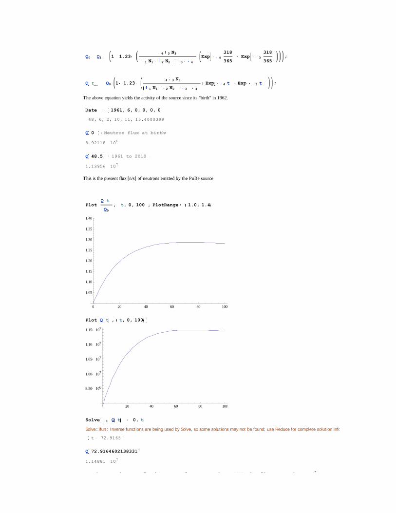
107
Q0 Q1 1 1.234 3 N3
1 N1 2 N2 3 4
Exp 4
318
365Exp 3
318
365;
Q t_ Q0 1 1.234 3 N3
1 N1 2 N2 3 4
Exp 4 t Exp 3 t ;
The above equation yields the activity of the source since its "birth" in 1962.
Date 1961, 6, 0, 0, 0, 0
48, 6, 2, 10, 11, 15.4000399
Q 0 Neutron flux at birth
8.92118 106
Q 48.5 1961 to 2010
1.13956 107
This is the present flux [n/s] of neutrons emitted by the PuBe source
PlotQ t
Q0
, t, 0, 100 , PlotRange 1.0, 1.4
0 20 40 60 80 100
1.05
1.10
1.15
1.20
1.25
1.30
1.35
1.40
Plot Q t , t, 0, 100
20 40 60 80 100
9.50 106
1.00 107
1.05 107
1.10 107
1.15 107
Solve t Q t 0, t
Solve::ifun : Inverse functions are being used by Solve, so some solutions may not be found; use Reduce for complete solution information.
t 72.9165
Q 72.9164602138331`
1.14881 107
Note of Interest: The source will reach its maximum flux sometime in the year 2033 and it will be approximately 1.15 x10⁷n/s

108
Appendix D: MCNP Code for Neutron Howitzer Design
D.1 Aluminum Howitzer
Howitzer nominal dimensions for thermal neutron generation c Cell cards for problem 2 0 (1:-7:15) $Void outside OD of can, top of can, btm of can 3 1 -7.82 (-1 2 -15 8 -21):(-1 7 -8):(21 -1 2 -15 8 18) $Steel can 4 3 -0.93 (-2 3 -15 14):(-2 5 -14 11 -21):(-2 3 -11 9):(-2 8 -9) & :(-2 -14 11 5 18) $Paraffin in can 5 3 -0.93 (-11 16 -4) $Paraffin UNDER source inside inner cylinder 6 3 -0.93 (-4 14 -15) $Paraffin OVER source inside inner cylinder 7 4 -0.001205 (-17 -2 6 21) $Air in beam tube 8 4 -0.001205 (12 -13 -6) $Air in manifold 9 4 -0.001205 (-16 10 -4) $Air under source in inner tube 10 2 -2.7 (-18 17 -1 6 21) $Aluminum inside beam tube 11 2 -2.7 (6 -5 -13 12 -21):(13 -14 4 -5): & (11 -12 4 -5):(21 6 -5 18 -13 11) $Aluminum inside manifold walls 12 2 -2.7 (-3 4 -15 14) $Aluminum inside inner tube above manifold 13 2 -2.7 (-3 4 -11 10):(-3 -10 9) $Aluminum inside inner tube below manifold 14 4 -0.001205 (-4 -14 13) $Air at TOP of manifold thickness 15 4 -0.001205 (-4 -12 11) $Air at BOTTOM of manifold thickness 16 4 -0.001205 (-17 -1 2 21) $Air in beam tube at end for flux count c End of cell cards c Beginning of surfaces 1 CZ 29.21 $OD of Can cylinder of radius 29.21 cm centered at origin 2 CZ 29.088588 $ID of Can cylinder of radius 29.08 cm centered at origin 3 CZ 2.8575 $OD of inside cylinder 4 CZ 2.54 $ID of inside cylinder 5 CZ 5.08 $OD of manifold 6 CZ 4.5974 $ID of manifold 7 PZ 0 $Bottom of can 8 PZ 0.121412 $Inside bottom of can 9 PZ 20.32 $Bottom of inner cylinder 10 PZ 20.8026 $Inside bottom of inner cylinder 11 PZ 31.75 $Bottom of manifold 12 PZ 32.2326 $Inside bottom of manifold 13 PZ 41.4274 $Top inside of manifold 14 PZ 41.91 $Top of manifold outside edge 15 PZ 73.66 $Top of poured wax in can 16 PZ 29.21 $Low edge of wax between PuBe and bottom of inner tube 17 C/X 0 36.83 2.07518 $ID of neutron beam tube 18 C/X 0 36.83 2.2225 $OD of neutron beam tube 19 PX 29.21 $Outside end of beam tube
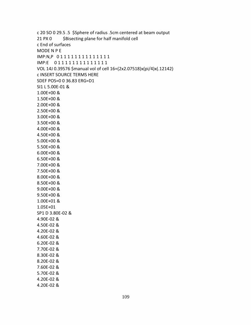
109
c 20 SO 0 29.5 .5 $Sphere of radius .5cm centered at beam output 21 PX 0 $Bisecting plane for half manifold cell c End of surfaces MODE N P E IMP:N,P 0 1 1 1 1 1 1 1 1 1 1 1 1 1 1 IMP:E 0 1 1 1 1 1 1 1 1 1 1 1 1 1 1 VOL 14J 0.39576 $manual vol of cell 16=(2x2.07518)x(pi/4)x(.12142) c INSERT SOURCE TERMS HERE SDEF POS=0 0 36.83 ERG=D1 SI1 L 5.00E-01 & 1.00E+00 & 1.50E+00 & 2.00E+00 & 2.50E+00 & 3.00E+00 & 3.50E+00 & 4.00E+00 & 4.50E+00 & 5.00E+00 & 5.50E+00 & 6.00E+00 & 6.50E+00 & 7.00E+00 & 7.50E+00 & 8.00E+00 & 8.50E+00 & 9.00E+00 & 9.50E+00 & 1.00E+01 & 1.05E+01 SP1 D 3.80E-02 & 4.90E-02 & 4.50E-02 & 4.20E-02 & 4.60E-02 & 6.20E-02 & 7.70E-02 & 8.30E-02 & 8.20E-02 & 7.60E-02 & 5.70E-02 & 4.20E-02 & 4.20E-02 &

110
5.20E-02 & 5.40E-02 & 5.10E-02 & 3.80E-02 & 1.70E-02 & 1.80E-02 & 2.20E-02 & 7.00E-03 c INSERT TALLY HERE F4:N 16 $avg flux in cell 16 (steel can thickness at beam end) E4 0 & $energy bins for the tally to count in MeV .025E-6 & .05E-6 & .1E-6 & .13E-6 & .2E-6 & .3E-6 & .4E-6 & .5E-6 & .6E-6 & .7E-6 & .8E-6 & .9E-6 & 1E-6 & 1 & 2 & 3 & 4 & 5 & 6 & 7 & 8 & 9 & 10 & 11 & 12 M1 6012 -0.005 26000 -0.995 $Steel M2 13027 1 $Aluminum M3 1001 -0.148605 6012 -0.851395 $Paraffin Wax M4 7014 .784437 6000 .000151 8016 .210750 18000 .004671 $Air NPS 5E6

111
D.2 PVC Howitzer
PVC Howitzer nominal dimensions for thermal neutron generation c Cell cards for problem 2 0 (1:-7:15) $Void outside OD of can, top of can, btm of can 3 1 -7.82 (-1 2 -15 8 -21):(-1 7 -8):(21 -1 2 -15 8 18) $Steel can 4 3 -0.93 (-2 3 -15 14):(-2 5 -14 11 -21):(-2 3 -11 9):(-2 8 -9) & :(-2 -14 11 5 18) $Paraffin in can 5 3 -0.93 (-11 16 -4) $Paraffin UNDER source inside inner cylinder 6 3 -0.93 (-4 14 -15) $Paraffin OVER source inside inner cylinder 7 4 -0.001205 (-17 -2 6 21) $Air in beam tube 8 4 -0.001205 (12 -13 -6) $Air in manifold 9 4 -0.001205 (-16 10 -4) $Air under source in inner tube 10 2 -1.406 (-18 17 -1 6 21) $PVC inside beam tube 11 2 -1.406 (6 -5 -13 12 -21):(13 -14 4 -5): & (11 -12 4 -5):(21 6 -5 18 -13 11) $PVC inside manifold walls 12 2 -1.406 (-3 4 -15 14) $PVC inside inner tube above manifold 13 2 -1.406 (-3 4 -11 10):(-3 -10 9) $PVC inside inner tube below manifold 14 4 -0.001205 (-4 -14 13) $Air at TOP of manifold thickness 15 4 -0.001205 (-4 -12 11) $Air at BOTTOM of manifold thickness 16 4 -0.001205 (-17 -1 2 21) $Air in beam tube at end for flux count c End of cell cards c Beginning of surfaces 1 CZ 29.21 $OD of Can cylinder of radius 29.21 cm centered at origin 2 CZ 29.088588 $ID of Can cylinder of radius 29.08 cm centered at origin 3 CZ 2.8575 $OD of inside cylinder 4 CZ 2.54 $ID of inside cylinder 5 CZ 5.08 $OD of manifold 6 CZ 4.5974 $ID of manifold 7 PZ 0 $Bottom of can 8 PZ 0.121412 $Inside bottom of can 9 PZ 20.32 $Bottom of inner cylinder 10 PZ 20.8026 $Inside bottom of inner cylinder 11 PZ 31.75 $Bottom of manifold 12 PZ 32.2326 $Inside bottom of manifold 13 PZ 41.4274 $Top inside of manifold 14 PZ 41.91 $Top of manifold outside edge 15 PZ 73.66 $Top of poured wax in can 16 PZ 29.21 $Low edge of wax between PuBe and bottom of inner tube 17 C/X 0 36.83 2.07518 $ID of neutron beam tube 18 C/X 0 36.83 2.2225 $OD of neutron beam tube 19 PX 29.20 $Outside end of beam tube

112
c 20 S 0 27 36.83 2 $Sphere of radius .5cm centered at beam output 21 PX 0 $Bisecting plane for half manifold cell c End of surfaces MODE N P E c IMP:N,P 0 1 1 1 1 1 1 1 1 1 1 c IMP:E 0 1 1 1 1 1 1 1 1 1 1 IMP:N,P 0 1 1 1 1 1 1 1 1 1 1 1 1 1 1 IMP:E 0 1 1 1 1 1 1 1 1 1 1 1 1 1 1 VOL 14J 0.4397 c INSERT SOURCE TERMS HERE SDEF POS=0 0 36.83 ERG=D1 SI1 L 5.00E-01 & 1.00E+00 & 1.50E+00 & 2.00E+00 & 2.50E+00 & 3.00E+00 & 3.50E+00 & 4.00E+00 & 4.50E+00 & 5.00E+00 & 5.50E+00 & 6.00E+00 & 6.50E+00 & 7.00E+00 & 7.50E+00 & 8.00E+00 & 8.50E+00 & 9.00E+00 & 9.50E+00 & 1.00E+01 & 1.05E+01 SP1 D 3.80E-02 & 4.90E-02 & 4.50E-02 & 4.20E-02 & 4.60E-02 & 6.20E-02 & 7.70E-02 & 8.30E-02 & 8.20E-02 & 7.60E-02 & 5.70E-02 &

113
4.20E-02 & 4.20E-02 & 5.20E-02 & 5.40E-02 & 5.10E-02 & 3.80E-02 & 1.70E-02 & 1.80E-02 & 2.20E-02 & 7.00E-03 c INSERT TALLY HERE F4:N 16 $avg flux in cell 16 (steel can thickness at beam end) E4 0 & $energy bins for the tally to count in MeV .025E-6 & .05E-6 & .1E-6 & .13E-6 & .2E-6 & .3E-6 & .4E-6 & .5E-6 & .6E-6 & .7E-6 & .8E-6 & .9E-6 & 1E-6 & 1 & 2 & 3 & 4 & 5 & 6 & 7 & 8 & 9 & 10 & 11 & 12 M1 6012 -0.005 26000 -0.995 $Steel M2 1001 -0.048382 6012 -0.384361 17000 -0.567257 $PVC pipe M3 1001 -0.148605 6012 -0.851395 $Paraffin Wax M4 7014 .784437 6000 .000151 8016 .210750 18000 .004671 $Air NPS 5E6

114
Appendix E: MCNP Code for Graphite Pile Differential Neutron Flux
E.1 Differential Neutron Flux at the diode
Pile minus a half-stringer for neutron flux on diode c Cell cards for problem 2 0 (-1:2:-4:7:8:-11) $Void outside pile c Diode Box 3 3 -2.7 (12 -13 15 -14 -17 16) $silicon filled c Missing Stringer 4 2 -0.001205 (-5 6 3 -2 -9 10)#(12 -13 15 -14 -17 16) $air filled c Graphite pile minus missing stringer 5 1 -1.7 (-8 9 -2 1 4 -7):(-10 11 -2 1 4 -7):(-9 10 4 -6 1 -2): & (-9 10 5 -7 1 -2):(-9 10 1 -3 6 -5) $graphite filled c End of cell cards c Beginning of surfaces c Top View of Pile, origin is pt source location 1 PX -63.5 $122 solid left wall 2 PX 63.5 $122 holed right wall 3 PX -5.5 $inside wall of missing stringer 4 PY -66 $127 upper wall 5 PY 5 $top of removed stringer hole 6 PY -5 $bottom of removed stringer hole 7 PY 56 $127 bottom wall c Side View of Pile 8 PZ 147 $top of Pile 9 PZ 20 $top of removed stringer hole 10 PZ 10 $bottom of removed stringer hole 11 PZ -35.5 $bottom of pile c Diode box for flux measurement 12 PX -0.5 13 PX 0.5 14 PY 0.5 15 PY -0.5 16 PZ 12.7 17 PZ 13.7 c End of surfaces MODE N P E c IMP:N,P 0 1 1 c IMP:E 0 1 1 IMP:N,P 0 1 1 1
115
IMP:E 0 1 1 1 VOL 1J 1.000 $manually entered volume of diode box as 1 cm3 SDEF POS=0 0 9 ERG=D1 SI1 L 5.00E-01 & 1.00E+00 & 1.50E+00 & 2.00E+00 & 2.50E+00 & 3.00E+00 & 3.50E+00 & 4.00E+00 & 4.50E+00 & 5.00E+00 & 5.50E+00 & 6.00E+00 & 6.50E+00 & 7.00E+00 & 7.50E+00 & 8.00E+00 & 8.50E+00 & 9.00E+00 & 9.50E+00 & 1.00E+01 & 1.05E+01 SP1 D 3.80E-02 & 4.90E-02 & 4.50E-02 & 4.20E-02 & 4.60E-02 & 6.20E-02 & 7.70E-02 & 8.30E-02 & 8.20E-02 & 7.60E-02 & 5.70E-02 & 4.20E-02 & 4.20E-02 & 5.20E-02 & 5.40E-02 & 5.10E-02 & 3.80E-02 & 1.70E-02 & 1.80E-02 &

116
2.20E-02 & 7.00E-03 c INSERT TALLY HERE F4:N 3 $avg flux in cell 3, diode box E4 0 & $energy bins for the tally to count in MeV .025E-6 & .05E-6 & .1E-6 & .13E-6 & .2E-6 & .3E-6 & .4E-6 & .5E-6 & .6E-6 & .7E-6 & .8E-6 & .9E-6 & 1E-6 & 1 & 2 & 3 & 4 & 5 & 6 & 7 & 8 & 9 & 10 & 11 & 12 M1 6012 -1 $Graphite M2 7014 .784437 6000 .000151 8016 .210750 18000 .004671 $Air M3 14000 -1 $Silicon NPS 1E8

117
E.2 Differential Neutron Flux at the diode with a Cd absorber
Pile minus a half-stringer for neutron flux on diode c Uses sphere and Cd covering c Cell cards for problem 2 0 (-1:2:-4:7:8:-11) $Void outside pile c Diode Ball 3 3 -2.7 (-18) $silicon filled sphere c 3 3 -2.7 (12 -13 15 -14 -17 16) $silicon filled box c Missing Stringer 4 2 -0.001205 (-5 6 3 -2 -9 10)#(-19) $air filled except Cd cover c 4 2 -0.001205 (-5 6 3 -2 -9 10)#(12 -13 15 -14 -17 16) $air filled c Graphite pile minus missing stringer 5 1 -1.7 (-8 9 -2 1 4 -7):(-10 11 -2 1 4 -7):(-9 10 4 -6 1 -2): & (-9 10 5 -7 1 -2):(-9 10 1 -3 6 -5) $graphite filled c Cadmium cover over diode ball 6 4 -8.65 (-19 18) $cadmium cover over diode sphere c End of cell cards c Beginning of surfaces c Top View of Pile, origin is pt source location 1 PX -63.5 $122 solid left wall 2 PX 63.5 $122 holed right wall 3 PX -5.5 $inside wall of missing stringer 4 PY -66 $127 upper wall 5 PY 5 $top of removed stringer hole 6 PY -5 $bottom of removed stringer hole 7 PY 56 $127 bottom wall c Side View of Pile 8 PZ 147 $top of Pile 9 PZ 20 $top of removed stringer hole 10 PZ 10 $bottom of removed stringer hole 11 PZ -35.5 $bottom of pile c Diode box for flux measurement 18 SZ 13.2 0.620345 $Sphere of r=.620345,vol=1, ctrd in 'diode box' 19 SZ 13.2 0.69655 $r= 0.6203 + 0.0763(0.03") = .69655 cm radius of Cd c End of surfaces MODE N P E IMP:N,P 0 1 1 1 1 IMP:E 0 1 1 1 1 VOL 1J 1.000 $manually entered volume of diode box as 1 cm3 SDEF POS=0 0 9 ERG=D1
118
SI1 L 5.00E-01 & 1.00E+00 & 1.50E+00 & 2.00E+00 & 2.50E+00 & 3.00E+00 & 3.50E+00 & 4.00E+00 & 4.50E+00 & 5.00E+00 & 5.50E+00 & 6.00E+00 & 6.50E+00 & 7.00E+00 & 7.50E+00 & 8.00E+00 & 8.50E+00 & 9.00E+00 & 9.50E+00 & 1.00E+01 & 1.05E+01 SP1 D 3.80E-02 & 4.90E-02 & 4.50E-02 & 4.20E-02 & 4.60E-02 & 6.20E-02 & 7.70E-02 & 8.30E-02 & 8.20E-02 & 7.60E-02 & 5.70E-02 & 4.20E-02 & 4.20E-02 & 5.20E-02 & 5.40E-02 & 5.10E-02 & 3.80E-02 & 1.70E-02 & 1.80E-02 & 2.20E-02 & 7.00E-03 c INSERT TALLY HERE
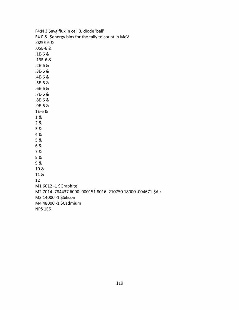
119
F4:N 3 $avg flux in cell 3, diode 'ball' E4 0 & $energy bins for the tally to count in MeV .025E-6 & .05E-6 & .1E-6 & .13E-6 & .2E-6 & .3E-6 & .4E-6 & .5E-6 & .6E-6 & .7E-6 & .8E-6 & .9E-6 & 1E-6 & 1 & 2 & 3 & 4 & 5 & 6 & 7 & 8 & 9 & 10 & 11 & 12 M1 6012 -1 $Graphite M2 7014 .784437 6000 .000151 8016 .210750 18000 .004671 $Air M3 14000 -1 $Silicon M4 48000 -1 $Cadmium NPS 1E6

120
Appendix F: Source and Detector Data Sheets
F.1 PuBe Source.
The following specifications were used for AFIT source T022.

121
F.2 Co-60 Source

122
F.3 LaBr(Ce) Detector Data Sheets
123
Appendix G: BF3 Calculations
G.1 Calculated thermal neutron flux using a BF3 detector
% Plot the 1 inch windowed thick Cd cover BF3 Data clear all close all clc Back1Gap = xlsread('BF3ThickSpectraData.xlsx', 'BF3ThickBack1Gap'); BackNoGap = xlsread('BF3ThickSpectraData.xlsx', 'BF3ThickBackNoGap'); BF3PileUp = xlsread('BF3ThickSpectraData.xlsx', 'BF3ThickPile1InchUp'); BF3PileDown = xlsread('BF3ThickSpectraData.xlsx',
'BF3ThickPile1InchDn'); BF3PileCdUp = xlsread('BF3ThickSpectraData.xlsx', 'BF3PileCdUp'); BF3PileCdDown = xlsread('BF3ThickSpectraData.xlsx', 'BF3PileCdDn'); %% Calculate macroscopic Cross-section R = 0.0820574587; %L atm / K mol T = 305.3; %90 F P = 0.9; %atm VoverN = R*T*(1/P)*1000; %cm3/mol B10Xsection = 3840E-24; %cm2/atom for thermal neutrons Sigma = (6.02E23/VoverN)*B10Xsection; %1/cm %% PLOT BACK OF HOWITZER DATA, PuBe Up Only BackCount = Back1Gap-BackNoGap; BackCount(:,1) = Back1Gap(:,1); %put the first column back in for i = 1:1024 if BackCount(i,2) < 0 BackCount(i,2) = 0; end end BackCountTotal = sum( BackCount(80:1023,2) ); BackCountPerSec = BackCountTotal/3600; OD = 1.008; %in WallThick = 0.0825; %inch BackCountWindow = 1; %inch BackCountActVol = (pi*((OD/2)-WallThick)^2*BackCountWindow)*16.387064;
%in3 to cm3 BackCountFlux = BackCountTotal*(1/3600)*(1/BackCountActVol)*(1/Sigma); figure(1) plot( BackCount(:,1),BackCount(:,2),'-' ); xlabel('Channel'); ylabel('Count'); set(gca,'XMinorTick','on') axis([70 500 0 5500]); legend('5.25" back, 17" up, Source Up: 57cps, 75[n/cm2 s]',2); hold on plot( Back1Gap(:,1),Back1Gap(:,2),'.-' ); hold on plot( BackNoGap(:,1),BackNoGap(:,2),'.-' ); %% PLOT FRONT OF HOWITZER DATA PuBe in down positions with 1" window Down = BF3PileDown-BF3PileCdDown; Down(:,1) = BF3PileDown(:,1); %put the first column back in for i = 1:1024 if Down(i,2) < 0 Down(i,2) = 0;
124
end end DownTotal = sum( Down(75:1023,2) ); DownPerSec = DownTotal/3600; FrontCountWindow = 1; %inch FrontCountActVol = (pi*((OD/2)-
WallThick)^2*FrontCountWindow)*16.387064; %in3 to cm3 FrontCountFluxDn = DownTotal*(1/3600)*(1/FrontCountActVol)*(1/Sigma); figure(2) plot( Down(:,1),Down(:,2),'-' ); xlabel('Channel'); ylabel('Count'); set(gca,'XMinorTick','on') axis([70 500 0 6500]); legend('At Diode, PuBe Dn: 61cps, 81[n/cm2 s]',2); hold on plot( BF3PileDown(:,1),BF3PileDown(:,2),'.-' ); hold on plot( BF3PileCdDown(:,1),BF3PileCdDown(:,2),'.-' ); %% PLOT FRONT OF HOWITZER DATA PuBe in Up position, 1" window Up = BF3PileUp-BF3PileCdUp; Up(:,1) = BF3PileUp(:,1); %put the first column back in for i = 1:1024 if Up(i,2) < 0 Up(i,2) = 0; end end UpTotal = sum( Up(75:1023,2) ); UpPerSec = UpTotal/3600; UpOpen = sum( BF3PileUp(75:1023,2) ); UpCd = sum( BF3PileCdUp(75:1023,2) ); UpNet = UpOpen-UpCd; FluxUp = UpTotal*(1/3600)*(1/FrontCountActVol)*(1/Sigma); figure('Color',[1 1 1]); plot( Up(:,1),Up(:,2),'k' ); xlabel('Channel'); ylabel('Count'); set(gca,'XMinorTick','on') axis([70 500 0 12000]); legend('At Diode, PuBe Up: 129cps, 170[n/cm2 s]',2); hold on plot( BF3PileUp(:,1),BF3PileUp(:,2),'--b' ); hold on plot( BF3PileCdUp(:,1),BF3PileCdUp(:,2),':r' ); h = legend('Net Counts','Cd Covered Tube Counts','Open Tube Counts',0); figure('Color',[1 1 1]); plot( Up(:,1),Up(:,2),'k' ); xlabel('Channel'); ylabel('Count'); set(gca,'XMinorTick','on') axis([70 500 0 12000]); legend('At Diode, PuBe Up: 129cps, 170[n/cm2 s]',2); h = legend('BF3 Tube Net Counts',0);
125
G.2 Neutron attenuation of the Cd shield
% Plot the I vs Io for neutron attenuation of Cd clear all close all clc CdXsxn = xlsread('BandCdXsections.xls', 'CdNAT'); figure(1) loglog( CdXsxn(:,1),CdXsxn(:,2),'-' ); ylabel('Cross-Section [b]'); xlabel('Energy [MeV]'); set(gca,'XMinorTick','on') legend('Natural Cd Neutron Cross Section',1); %Choose energies below 10 eV, convert to eV, convert b to cm2 for i=1:5467 if CdXsxn(i,1) <= 1E-5 % 10eV is 1E-5MeV CdX(i,1) = CdXsxn(i,1)*1E6; %convert to eV from MeV CdX(i,2) = CdXsxn(i,2)*1E-24; % b to cm2 end end figure(2) loglog( CdX(:,1),CdX(:,2),'-' ); ylabel('Cross-Section [cm2]'); xlabel('Energy [eV]'); set(gca,'XMinorTick','on') legend('Natural Cd Neutron Cross Section',1); %% Cd thickness x = 0.3277; %cm .043"=.10922 cm times 3 is .3277 %% Sigma NA = 6.02E23; %atom/mol rho = 8.648; %g/cm3 mw = 112.411; %g/mol N = rho*NA*(1/mw); %nuclei/cm3 for i = 1:172 IoverINot(i,1) = CdX(i,1); %first column is energy IoverINot(i,2) = exp( -CdX(i,2).*N.*x ); %second column is I/Io end for i = 1:172 IoverINot1(i,1) = CdX(i,1); %first column is energy IoverINot1(i,2) = exp( -CdX(i,2).*N.*x/3 ); %second column is I/Io end for i = 1:172 IoverINot2(i,1) = CdX(i,1); %first column is energy IoverINot2(i,2) = exp( -CdX(i,2).*N.*x/10 ); %second column is I/Io end figure('Color',[1 1 1]); plot( IoverINot(:,1),IoverINot(:,2),'k' ); hold on plot( IoverINot1(:,1),IoverINot1(:,2),':k' ); hold on plot( IoverINot2(:,1),IoverINot2(:,2),'--k' ); xlabel('Energy [eV]'); set(gca,'XMinorTick','on') h = legend('0.33cm Cd','0.11cm Cd','0.033cm Cd',0); axis([.025 5 0 1]);

126
G.3 Calibration of the BF3 Tube using the Standard Graphite Pile
% Calibrate the BF3 Tube using the graphite pile % This will determine an efficiency factor for the Tube as configured clear all close all clc % Input Standard Data OldD4stdFlux = 5720; % n /cm2 s FROM AFIT STD PILE TM OldD3stdFlux = 7920; % n /cm2 s FROM AFIT STD PILE TM OldD2stdFlux = 6920; % n /cm2 s FROM AFIT STD PILE TM PuBeActivity1961 = 8.92118E6; % n/s FROM MATHEMATICA PGM PuBeActivity2009 = 1.13956E7; % n/s OD = 1.008; %inch, BF3 Parameter WallThick = 0.0825; %inch, BF3 Parameter Window = 1; %inch, BF3 Parameter % Input Pile Experimental Data D4rawBF3win = 82901590; % cts D3rawBF3win = 114887792; % cts D2rawBF3win = 96523485; % cts **UPDATE THIS** D4rawBF3cvrd = 28423306; % cts D3rawBF3cvrd = 54636873; % cts D2rawBF3cvrd = 49004385; % cts **UPDATE THIS** PHStime = 3600; %s % Calculate Corrected Flux to current PuBe activity FM = PuBeActivity2009/PuBeActivity1961; D4stdFlux = OldD4stdFlux*FM; % n /cm2 s D3stdFlux = OldD3stdFlux*FM; % n /cm2 s D2stdFlux = OldD2stdFlux*FM; % n /cm2 s % Calculate macroscopic Cross-section R = 0.0820574587; %L atm / K mol T = 305.3; %90 F P = 0.9; %atm VoverN = R*T*(1/P)*1000; %cm3/mol B10Xsection = 3840E-24; %cm2/atom for thermal neutrons Sigma = (6.02E23/VoverN)*B10Xsection; %1/cm % Calculate D4 Measured Flux D4ActiveVol = (pi*((OD/2)-WallThick)^2*Window)*16.387064; %in3 to cm3 D4ExpFlux = (D4rawBF3win-
D4rawBF3cvrd)*(1/PHStime)*(1/D4ActiveVol)*(1/Sigma); %n/cm2 s % Calculate D3 Measured Flux D3ActiveVol = (pi*((OD/2)-WallThick)^2*Window)*16.387064; %in3 to cm3 D3ExpFlux = (D3rawBF3win-
D3rawBF3cvrd)*(1/PHStime)*(1/D3ActiveVol)*(1/Sigma); %n/cm2 s % Calculate D2 Measured Flux D2ActiveVol = (pi*((OD/2)-WallThick)^2*Window)*16.387064; %in3 to cm3 D2ExpFlux = (D2rawBF3win-
D2rawBF3cvrd)*(1/PHStime)*(1/D2ActiveVol)*(1/Sigma); %n/cm2 s %% Plot the Standard and Measured Flux Data figure('Color',[1 1 1]); xlabel('Pile Position (Drawer)'); ylabel('Thermal Neutron Flux [n/cm2 s]'); bar( [D2stdFlux,D2ExpFlux; D3stdFlux,D3ExpFlux; D4stdFlux,D4ExpFlux]); set(gca,'XTickLabel',2:4) xlabel('Pile Position (Drawer)');

127
ylabel('Thermal Neutron Flux [n/cm2 s]'); h=legend('Calibrated 0.025 eV flux in Graphite Pile','BF3 Uncalibrated
Flux', 0); %% Determine an efficiency factor for the BF3 Tube D4efficiency = D4stdFlux/D4ExpFlux; %this (x100) efficiency at D4
**CHECK THIS** D3efficiency = D3stdFlux/D3ExpFlux; D2efficiency = D2stdFlux/D2ExpFlux; AvgEfficiency = (D4efficiency+D3efficiency+D2efficiency)/3;

128
Appendix H: Sr-90 Experiment Calculations
H.1 Determine the Beta flux into the diode from the Sr-90source
%Determine the Beta Flux into the Diode from Sr-90 clear all close all clc
Dist_in = 0.75;%1.375; %Source to detector distance [in] Sr90_Ci = 0.005973; %Current Sr90 activity [Ci], 25mCi on 28 Feb 1951
Sr90_Bq = Sr90_Ci * 3.7E10; % [Bq] Dist_cm = Dist_in * 2.54; % [cm] Air_rho = .0012; %[g/cm3] Gd2O3_rho = 7.41; %[g/cm3] Al_rho = 2.7; %[g/cm3] Au_rho = 19.3; %[g/cm3] SS_rho = 8; %[g/cm3] Al_thick_cm = 0.000002 + 0.0254; %[cm] (contact + 10mil source window) SS_thick_cm = 0.00508; %[cm] (2 mil Stainless Steel) Au_thick_cm = 0.000005; %[cm] Gd2O3_thick_cm = 0.000159; %[cm] thickness of non-depleted Gd2O3
Gamma_196_init = 195.8; %initial average beta energy from Sr90 [kev] Gamma_934_init = 933.7; %initial average beta energy from Y90 [kev]
%% Air Loss CSDA_196_air = 5.0E-2;% [g/cm3] Range_196_air = CSDA_196_air / Air_rho; %(g/cm2)(cm3/g)=[cm] SP_196_air = 2474 * Air_rho; %(kev cm2/g)(g/cm3)=[keV/cm] CSDA_934_air = .4316;% [g/cm3] Range_934_air = CSDA_934_air / Air_rho; %(g/cm2)(cm3/g)=[cm] SP_934_air = 1681 * Air_rho; %(kev cm2/g)(g/cm3)=[keV/cm] %% Al Loss CSDA_196_al = 5.8E-2;% [g/cm3] Range_196_al = CSDA_196_al / Al_rho; %(g/cm2)(cm3/g)=[cm] SP_196_al = 2183 * Al_rho; %(kev cm2/g)(g/cm3)=[keV/cm] CSDA_934_al = .4874;% [g/cm3] Range_934_al = CSDA_934_al / Al_rho; %(g/cm2)(cm3/g)=[cm] SP_934_al = 1492 * Al_rho; %(kev cm2/g)(g/cm3)=[keV/cm] %% Au Loss CSDA_196_au = 9.004E-2;% [g/cm3] Range_196_au = CSDA_196_au / Au_rho; %(g/cm2)(cm3/g)=[cm] SP_196_au = 1466 * Au_rho; %(kev cm2/g)(g/cm3)=[keV/cm] CSDA_934_au = .6873;% [g/cm3] Range_934_au = CSDA_934_au / Au_rho; %(g/cm2)(cm3/g)=[cm] SP_934_au = 1122 * Au_rho; %(kev cm2/g)(g/cm3)=[keV/cm] %% SS Loss CSDA_196_SS = 6.556E-02;%[g/cm2] Iron Range_196_SS = CSDA_196_SS / SS_rho; %(g/cm2)(cm3/g)=[cm] SP_196_SS = 1947 * SS_rho; %(kev cm2/g)(g/cm3)=[keV/cm] CSDA_934_SS = 5.420E-01;% [g/cm2] Range_934_SS = CSDA_934_SS / SS_rho; %(g/cm2)(cm3/g)=[cm] SP_934_SS = 1354 * SS_rho; %(kev cm2/g)(g/cm3)=[keV/cm]

129
%% Gadolina Loss (Uranium Oxide Proxy) CSDA_196_Gd2O3 = 8.854E-2;% [g/cm3] Range_196_Gd2O3 = CSDA_196_Gd2O3 / Gd2O3_rho; %(g/cm2)(cm3/g)=[cm] SP_196_Gd2O3 = 1487 * Gd2O3_rho; %(kev cm2/g)(g/cm3)=[keV/cm] CSDA_934_Gd2O3 = .6778;% [g/cm3] Range_934_Gd2O3 = CSDA_934_Gd2O3 / Gd2O3_rho; %(g/cm2)(cm3/g)=[cm] SP_934_Gd2O3 = 1136 * Gd2O3_rho; %(kev cm2/g)(g/cm3)=[keV/cm] %% Stopping Power, Beta at Deposition Energy, non-E-loss Estimate E_loss_196 = (SP_196_air*Dist_cm) + (SP_196_al*Al_thick_cm) +
(SP_196_au*Au_thick_cm )... +(SP_196_Gd2O3*Gd2O3_thick_cm) + (SP_196_SS*SS_thick_cm) ; %
(keV/cm)(cm) = [keV] E_loss_934 = (SP_934_air*Dist_cm) + (SP_934_al*Al_thick_cm) +
(SP_934_au*Au_thick_cm )... +(SP_934_Gd2O3*Gd2O3_thick_cm)+(SP_934_SS*SS_thick_cm); %
(keV/cm)(cm) = [keV]
SP_alum_drop_196 = SP_196_al*Al_thick_cm; SP_alum_drop_934 = SP_934_al*Al_thick_cm; SP_SS_drop_196 = SP_196_SS*SS_thick_cm; SP_SS_drop_934 = SP_934_SS*SS_thick_cm;
Gamma_196_finalSP = Gamma_196_init - E_loss_196; %[keV] Gamma_934_finalSP = Gamma_934_init - E_loss_934; %[keV] % This does not account for the fact that the energy is lowered at each % step which will adjust the stopping powers %% CSDA approximation Drop_196_air = (Gamma_196_init / Range_196_air)*(Dist_cm);
%(keV/cm)(cm)=[keV] Drop_934_air = (Gamma_934_init / Range_934_air)*(Dist_cm);
%(keV/cm)(cm)=[keV] Drop_196_al = (Gamma_196_init / Range_196_al)*(Al_thick_cm);
%(keV/cm)(cm)=[keV] Drop_934_al = (Gamma_934_init / Range_934_al)*(Al_thick_cm);
%(keV/cm)(cm)=[keV] Drop_196_SS = (Gamma_196_init / Range_196_SS)*(SS_thick_cm);
%(keV/cm)(cm)=[keV] Drop_934_SS = (Gamma_934_init / Range_934_SS)*(SS_thick_cm);
%(keV/cm)(cm)=[keV] Drop_196_au = (Gamma_196_init / Range_196_au)*(Au_thick_cm);
%(keV/cm)(cm)=[keV] Drop_934_au = (Gamma_934_init / Range_934_au)*(Au_thick_cm);
%(keV/cm)(cm)=[keV] Drop_196_Gd2O3 = (Gamma_196_init / Range_196_Gd2O3)*(Gd2O3_thick_cm);
%(keV/cm)(cm)=[keV] Drop_934_Gd2O3 = (Gamma_934_init / Range_934_Gd2O3)*(Gd2O3_thick_cm);
%(keV/cm)(cm)=[keV] Gamma_196_final_CSDA = (Gamma_196_init)-
(Drop_196_air+Drop_196_al+Drop_196_SS+Drop_196_au+Drop_196_Gd2O3);
%[keV] Gamma_934_final_CSDA = (Gamma_934_init)-
(Drop_934_air+Drop_934_al+Drop_934_SS+Drop_934_au+Drop_934_Gd2O3);
%[keV]
%% Results

130
% Beta energy blocked by 1.375" air and aluminum/SS window Al_Block_196 = SP_alum_drop_196; Al_Block_934 = SP_alum_drop_934; Air_Block_196 = (SP_196_air*1.375); Air_Block_934 = (SP_934_air*1.375); SS_Block_196 = SP_SS_drop_196; SS_Block_934 = SP_SS_drop_934; No_Fraction_196 = Al_Block_196 + Air_Block_196 + SP_SS_drop_196;
No_Fraction_934 = Al_Block_934 + Air_Block_934 + SP_SS_drop_934; %% R-Squared for Beta flux on diode R2 = (Dist_cm)^2; %cm2 Basic_Flux = (Sr90_Bq * 2) / R2; %Beta/cm2 s, ignores low energy cut-
off %% Determine advanced flux and Beta energies Q1 = 546; %[keV] Q2 = 2280.1; %[keV] Q1_cutoff = 500;% 204; %set temp for nice plot...299; %this is the
energy of the betas that don't make it Q2_cutoff = 500;%204; step_size = 1; %[keV] i=0; Big_C = 1; %Matrix constant set equal to 1 c = 9.8; %[m/s] mc2 = 511; %[keV] %Q1 for i = 1:(Q1/step_size) T = step_size * i; Q1_spectrum(i,1) = T; Q1_spectrum(i,2) = ((Big_C)/c^5)*((T^2 + 2*T*mc2)^.5)*((Q1-
T)^2)*(T+mc2); %(1/keV){(keV)^2 + (keV)(keV)}^.5 (keV)^2 *keV = [kev]^4/[m/s]^5 end Num_Integrate_Q1 = sum(Q1_spectrum(:,2)); Q1_spectrum(:,3) = Q1_spectrum(:,2)/Num_Integrate_Q1; %check the normalized distribution check = sum(Q1_spectrum(:,3)); %should equal unity %% figure('Color',[1 1 1]); plot( Q1_spectrum(:,1), Q1_spectrum(:,3),'k' ) % position 3 is
normalized xlabel('Te[keV]'); ylabel('N(Te), normalized'); hold on for i = 1:(Q1/step_size) if Q1_spectrum(i,1) <= Q1_cutoff Q1_spectrum(i,4) = 0; else Q1_spectrum(i,4) = Q1_spectrum(i,3); end end %figure(2) area( Q1_spectrum(:,1), Q1_spectrum(:,4),'FaceColor',[0.0,0.0,0.0]) Transmitted_fraction = sum(Q1_spectrum(:,4)); %the normalized fraction emitted = [0.220222563676303] %Q2 for i = 1:(Q2/step_size)

131
T = step_size * i; Q2_spectrum(i,1) = T; Q2_spectrum(i,2) = ((Big_C)/c^5)*((T^2 + 2*T*mc2)^.5)*((Q2-
T)^2)*(T+mc2); end Num_Integrate_Q2 = sum(Q2_spectrum(:,2)); Q2_spectrum(:,3) = Q2_spectrum(:,2)/Num_Integrate_Q2; %check the normalized distribution check2 = sum(Q2_spectrum(:,3)); %should equal unity %% figure('Color',[1 1 1]); plot( Q2_spectrum(:,1), Q2_spectrum(:,3) ) xlabel('Te[keV]'); ylabel('N(Te), normalized'); hold on for i = 1:(Q2/step_size) if Q2_spectrum(i,1) <= Q2_cutoff Q2_spectrum(i,4) = 0; else Q2_spectrum(i,4) = Q2_spectrum(i,3); end end %% %figure(4) area( Q2_spectrum(:,1), Q2_spectrum(:,4),'FaceColor',[0.0,0.0,0.0]) Transmitted_fraction2 = sum(Q2_spectrum(:,4)); %the normalized fraction emitted = [0.959610083044573]
%Plot the fraction that actually transmits for i = 1:(Q1/step_size) Emit_Spectrum(i,1)= i; if Q1_spectrum(:,4) <= 0 then Emit_Spectrum(i,2)= 0; else Emit_Spectrum(i,2)= Q1_spectrum(i,4); end end for i = 1:(Q2/step_size) if Q2_spectrum(:,4) <= 0 then Emit_Spectrum(i,3)= 0; else Emit_Spectrum(i,3)= Q2_spectrum(i,4); end Emit_Spectrum(i,1) = i; %add empty colums for Q1 to equalize the
vectors end %% Emit_Spectrum(Q1/step_size:Q2/step_size,2) = 0; %Q1_spectrum(Q1/step_size:Q2/step_size,4) = 0; %figure(5) figure('Color',[1 1 1]); area( Emit_Spectrum(:,1), Emit_Spectrum(:,2) ) xlabel('Te[keV]'); ylabel('N(Te), normalized'); hold on area( Emit_Spectrum(:,1), Emit_Spectrum(:,3) ) %% figure('Color',[1 1 1]); %add the emitted fractions
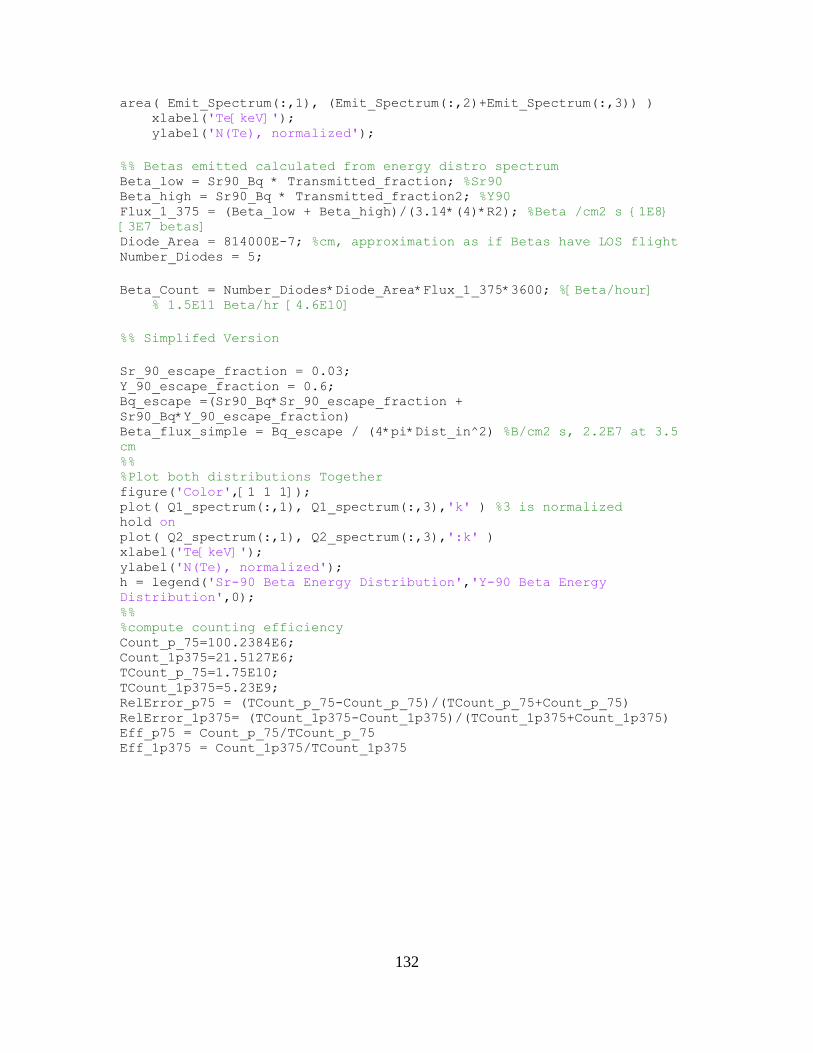
132
area( Emit_Spectrum(:,1), (Emit_Spectrum(:,2)+Emit_Spectrum(:,3)) ) xlabel('Te[keV]'); ylabel('N(Te), normalized');
%% Betas emitted calculated from energy distro spectrum Beta_low = Sr90_Bq * Transmitted_fraction; %Sr90 Beta_high = Sr90_Bq * Transmitted_fraction2; %Y90 Flux_1_375 = (Beta_low + Beta_high)/(3.14*(4)*R2); %Beta /cm2 s {1E8}
[3E7 betas] Diode_Area = 814000E-7; %cm, approximation as if Betas have LOS flight Number_Diodes = 5;
Beta_Count = Number_Diodes*Diode_Area*Flux_1_375*3600; %[Beta/hour] % 1.5E11 Beta/hr [4.6E10]
%% Simplifed Version
Sr_90_escape_fraction = 0.03; Y_90_escape_fraction = 0.6; Bq_escape =(Sr90_Bq*Sr_90_escape_fraction +
Sr90_Bq*Y_90_escape_fraction) Beta_flux_simple = Bq_escape / (4*pi*Dist_in^2) %B/cm2 s, 2.2E7 at 3.5
cm %% %Plot both distributions Together figure('Color',[1 1 1]); plot( Q1_spectrum(:,1), Q1_spectrum(:,3),'k' ) %3 is normalized hold on plot( Q2_spectrum(:,1), Q2_spectrum(:,3),':k' ) xlabel('Te[keV]'); ylabel('N(Te), normalized'); h = legend('Sr-90 Beta Energy Distribution','Y-90 Beta Energy
Distribution',0); %% %compute counting efficiency Count_p_75=100.2384E6; Count_1p375=21.5127E6; TCount_p_75=1.75E10; TCount_1p375=5.23E9; RelError_p75 = (TCount_p_75-Count_p_75)/(TCount_p_75+Count_p_75) RelError_1p375= (TCount_1p375-Count_1p375)/(TCount_1p375+Count_1p375) Eff_p75 = Count_p_75/TCount_p_75 Eff_1p375 = Count_1p375/TCount_1p375

133
H.2 Sr-90 Source Protocol
MEMORANDUM FOR RECORD 17 NOV 2009
SUBJECT: Protocol for Safety Review and Self Study Documentation
I am requesting that AFIT/ENP conduct a safety review of the experiment identified below. Title of Experiment: Gd2O3/Si diode interaction with beta-particles Principle Investigators: MAJ Chris Young Experiment’s Location: Basement of Bldg. 470, Neutron Room Personnel Involved: LTC John McClory Date of Previous Peer Review: None A self study was conducted and the hazards associated with the experiment are summarized below. Attached are all general guidelines, as well as experimental schematics. A copy of the WPAFB radiation guideline and this protocol will be posted at the experimental station. DESCRIPTION OF EXPERIMENT: The experiment is designed to determine if a novel diode made from Gd2O3 deposited on Si can successfully produce an electrical signal in the presence of beta-particles. Successful signal generation is desired to corroborate neutron interactions in which auger electrons are produced within the diode. Experimental procedures: 1. Personal Protective Equipment, Accountability, and Shielding: All radiation sources will remain in the location for which they are signed out. If the source must change locations (e.g. room), a qualified person must sign it out and into the new location. The use of the Sr-90 source (AFIT ID 00365) will require gloves and a lab coat. A survey meter with a beta-window will be used to check for any contamination of the experiment by the source once it is placed back into storage. Any surface that has the potential to be contaminated will be tested using a survey meter with beta-window to include PPE. Aluminum shielding 0.25” thick will be employed to protect personnel in the room from beta emissions. The experiment will take place in the neutron room of Bldg. 470. 2. Mounting: The source will rest on supports to facilitate a quick transition from storage into the shielded experiment area to reduce the time of exposure. 3. Measurements: The signal from the diode will be recorded through a series of amplifiers using a multi-channel analyzer.

134
4. Cleanup and Monitoring: Because the source is sealed but has the potential to leak, anything it comes in contact with will be monitored for possible contamination. All experimental hardware, PPE, and the floor surrounding the experiment will be interrogated with an appropriate, beta-sensitive, survey meter for signs of contamination. Any contamination found will be immediately reported to the RSO and the experiment halted. The source is leak tested every 6 months. The last test showed no leakage on 28 Aug 2009. SUMMARY OF MAJOR SAFETY ISSUES: Potential hazards are from Radioactive sources and High Voltages. DETAILED SAFETY ANALYSIS: Identify all hazardous chemicals use with this experiment. Identify the location of all stored chemicals: Identify all hazardous waste generated by this experiment: Identify all ventilation requirements: Identify all electrical hazards associated with this experiment: Identify all laser hazards associated with this experiment: Identify all source of ionizing radiation: The Sr-90 source has an activity of 6 mCi. The beta decay of Sr-90 emits beta particles
with an end-point energy of 546 keV. The daughter product, Y-90, also beta decays with
particles of end-point energy 2.27 MeV. The half-life of Sr-90 is 28.7 years. The half-
life of Y-90 is 64.1 hours. Identify all other safety or bio-environmental hazards: Sr-90 is a well-known bone-seeking compound due to its biological similarity to calcium. For this reason, proper PPE, handling procedures, and leak testing are used. Identify all available protective equipment: PPE: Lab coat, gloves, dosimetry. Shielding: For shielding requirements, the more energetic beta energies of Y-90 were considered with a range of 1.1 g/cm2 in air. Sea level air on a standard day has a density of 0.0012 g/cm3 (Cerber). The farthest traveling beta-particle would be stopped in air in 916 cm [(1.1 g/cm^2 / 0.0012 g/cc) = 916 cm]. Considering that the preponderance of beta-particles would be from the Sr-90 itself, the range of a 0.54 MeV beta has a range in air of 0.12 g/cm2 which will travel 100 cm. The source will only be handled to place it onto the experimental apparatus or put it back into its storage container. A 0.25 in plastic shield is fixed to the source handle and is designed to protect the user from beta radiation when holding the source. This shield will stop most of the expected beta particles but the most energetic betas (2.3 MeV) require 0.37 in of plexiglass (Cerber). Aluminum plate will also be used to shield the experiment from the researcher. 0.2 in of

135
Al will stop a 2.3 MeV beta particle. The aluminum that will be employed is 0.25 inches thick. The concrete floor and walls of the neutron room are thicker than the minimum 0.2 in required to stop the most energetic beta emission and will contain the sources effects to the lab. Identify all exposure monitors, alarms, or detectors: A Ludlum model 2224-1 ratemeter in conjuction with a Ludlum model 43-89 probe will be used to detect beta activity. Describe all emergency plans and procedure: In the case of an emergency, the radiation source being used will be shielded and secured prior to implementation of AFIT approved evacuation plan. In the event of a fire or other similar event, the investigator will ensure that the responders are aware of the additional consideration. The source is solid. Liquid spills will not be an issue. In the event of an accident or emergency, the RSO will be notified as quickly as possible. Identify all unresolved safety and bio-environmental issues: Identify and limitation currently imposed by safety issues: Recommendations for improving safety conditions: Miscellaneous Issues: I recommend conduction of this experiment as described and specified above. I am prepared to discuss this self study with the AFIT/ENP Safety Committee. Attachments: (*Omitted for this Appendix*) Attachment A: Guidelines for Working with Radioactive Material Attachment B: Guidelines for Working with High Voltage/High Current Equipment Attachment C: Basic Experimental Setup Attachment D: AFIT Radiation Safety Program Attachment E: WPAFB I 40-201 (2007) Attachment F: Drawing of Sr-90 Source MAJ Chris Young AFIT/ENP

136
Appendix I: MCNP Code for gamma ray energy deposition in the diode
I.1 Energy deposition in the diode from a PuBe photon spectrum
Energy deposition in cylinder diode from gamma source c Cell cards for problem 2 5 -0.001205 -11 10 -1 $ Free Air 3 5 -0.001205 -10 9 -1 $ air 4 5 -0.001205 -9 8 -1 $ Inner Air 5 1 -19.3 -8 7 -1 $ Gold Contact 6 2 -2.7 -7 6 -1 $ Al Contact 7 4 -7.41 -6 5 -1 $ non depleted Gd2O3 layer 8 4 -7.41 -5 4 -1 $ depleted Gd2O3 layer 9 3 -2.33 (-4 3 -1):(2 -3 -1) $ depleted Si layer and diffusion vol 10 0 (1:11:-2) $ VOID out cylinder, btm and top c End of cell cards c Beginning of surfaces 1 CZ .0407 $ cylinder of radius .0407 cm centered at origin 2 PZ -6.022E-3 $ Diffusion Length in Si 3 PZ 0 $ Si Depletion Distance 4 PZ 1.590E-4 $ Metallurgical Junction 5 PZ 1.592E-4 $ Gd2O3 Depletion Distance 6 PZ 1.6924E-4 $ Top of Gd2O3 and bottom of Al 7 PZ 1.712E-4 $ Top of Al, bottom of Au 8 PZ 1.762E-4 $ Top of Au, bottom of inner air 9 PZ 0.75 $ Top of inner Air, bottom of Cadmium 10 PZ 0.826 $ Top of Cadmium, bottom of free air 11 PZ 3.826 $ Top of free air and void start c End of surfaces MODE P E IMP:P 1 1 1 1 1 1 1 1 0 IMP:E 1 1 1 1 1 1 1 1 0 VOL 7J 1.61E-5 $ VOLUME of depletion+diff Length ***CHECK THIS*** SDEF POS=0 0 1 PAR=2 ERG=D1 $ ***Change position of SOURCE in X Y Z*** c GAMMA SPECTRUM SI1 L 2.0E-02 & 4.0E-02 & 6.0E-02 & 8.0E-02 & 1.0E-01 & 1.2E-01 & 1.4E-01 &

137
1.6E-01 & 1.8E-01 & 2.0E-01 & 2.2E-01 & 2.4E-01 & 2.6E-01 & 2.8E-01 & 3.0E-01 & 3.2E-01 & 3.4E-01 & 3.6E-01 & 3.8E-01 & 4.0E-01 & 4.2E-01 & 4.4E-01 & 4.6E-01 & 4.8E-01 & 5.0E-01 & 5.2E-01 & 5.4E-01 & 5.6E-01 & 5.8E-01 & 6.0E-01 & 6.2E-01 & 6.4E-01 & 6.6E-01 & 6.8E-01 & 7.0E-01 & 7.2E-01 & 7.4E-01 & 7.6E-01 & 7.8E-01 & 8.0E-01 & 8.2E-01 & 8.4E-01 & 8.6E-01 & 8.8E-01 & 9.0E-01 & 9.2E-01 & 9.4E-01 & 9.6E-01 & 9.8E-01 & 1.0E+00

138
SP1 D 3.2E-02 & 6.5E-03 & 4.9E-01 & 2.9E-02 & 9.7E-02 & 3.2E-02 & 9.7E-03 & 9.1E-03 & 8.1E-03 & 9.7E-03 & 6.5E-03 & 4.9E-03 & 4.9E-03 & 6.5E-03 & 9.7E-03 & 2.3E-03 & 6.5E-03 & 1.3E-03 & 1.9E-01 & 6.5E-03 & 1.6E-02 & 1.6E-03 & 9.7E-04 & 9.7E-04 & 6.5E-03 & 9.7E-04 & 6.5E-04 & 4.9E-04 & 4.9E-04 & 4.5E-04 & 4.5E-04 & 4.2E-04 & 4.2E-04 & 3.9E-04 & 3.9E-04 & 3.6E-04 & 3.6E-04 & 3.2E-04 & 3.2E-04 & 2.9E-04 & 2.9E-04 & 2.6E-04 & 2.6E-04 &

139
2.3E-04 & 2.3E-04 & 1.9E-04 & 1.9E-04 & 1.6E-04 & 1.6E-04 & 1.3E-04 c TALLY DATA F4:E 9 $Flux avg in cell 9, MeV/cm2, diff vol E4 0 & 2.0E-02 & 4.0E-02 & 6.0E-02 & 8.0E-02 & 1.0E-01 & 1.2E-01 & 1.4E-01 & 1.6E-01 & 1.8E-01 & 2.0E-01 & 2.2E-01 & 2.4E-01 & 2.6E-01 & 2.8E-01 & 3.0E-01 & 3.2E-01 & 3.4E-01 & 3.6E-01 & 3.8E-01 & 4.0E-01 & 4.2E-01 & 4.4E-01 & 4.6E-01 & 4.8E-01 & 5.0E-01 & 5.2E-01 & 5.4E-01 & 5.6E-01 & 5.8E-01 & 6.0E-01 & 6.2E-01 & 6.4E-01 & 6.6E-01 &

140
6.8E-01 & 7.0E-01 & 7.2E-01 & 7.4E-01 & 7.6E-01 & 7.8E-01 & 8.0E-01 & 8.2E-01 & 8.4E-01 & 8.6E-01 & 8.8E-01 & 9.0E-01 & 9.2E-01 & 9.4E-01 & 9.6E-01 & 9.8E-01 & 1.0E+00 c MATERIALS M1 79197 1 $Au M2 13027 1 $Al M3 14000 1 $Si M4 64000 2 8016 3 $Gd2O3 M5 7014 .784437 6000 .000151 8016 .210750 18000 .004671 $Air M6 48000 1 $Cadmium NPS 5E9
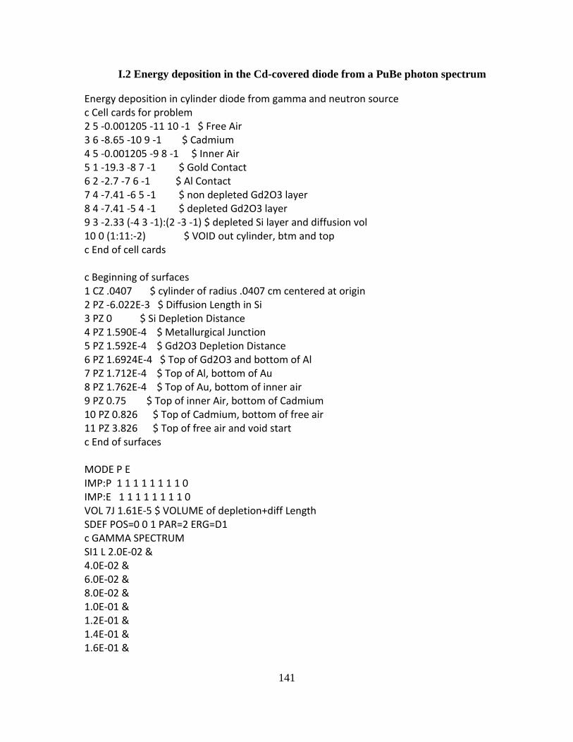
141
I.2 Energy deposition in the Cd-covered diode from a PuBe photon spectrum
Energy deposition in cylinder diode from gamma and neutron source c Cell cards for problem 2 5 -0.001205 -11 10 -1 $ Free Air 3 6 -8.65 -10 9 -1 $ Cadmium 4 5 -0.001205 -9 8 -1 $ Inner Air 5 1 -19.3 -8 7 -1 $ Gold Contact 6 2 -2.7 -7 6 -1 $ Al Contact 7 4 -7.41 -6 5 -1 $ non depleted Gd2O3 layer 8 4 -7.41 -5 4 -1 $ depleted Gd2O3 layer 9 3 -2.33 (-4 3 -1):(2 -3 -1) $ depleted Si layer and diffusion vol 10 0 (1:11:-2) $ VOID out cylinder, btm and top c End of cell cards c Beginning of surfaces 1 CZ .0407 $ cylinder of radius .0407 cm centered at origin 2 PZ -6.022E-3 $ Diffusion Length in Si 3 PZ 0 $ Si Depletion Distance 4 PZ 1.590E-4 $ Metallurgical Junction 5 PZ 1.592E-4 $ Gd2O3 Depletion Distance 6 PZ 1.6924E-4 $ Top of Gd2O3 and bottom of Al 7 PZ 1.712E-4 $ Top of Al, bottom of Au 8 PZ 1.762E-4 $ Top of Au, bottom of inner air 9 PZ 0.75 $ Top of inner Air, bottom of Cadmium 10 PZ 0.826 $ Top of Cadmium, bottom of free air 11 PZ 3.826 $ Top of free air and void start c End of surfaces MODE P E IMP:P 1 1 1 1 1 1 1 1 0 IMP:E 1 1 1 1 1 1 1 1 0 VOL 7J 1.61E-5 $ VOLUME of depletion+diff Length SDEF POS=0 0 1 PAR=2 ERG=D1 c GAMMA SPECTRUM SI1 L 2.0E-02 & 4.0E-02 & 6.0E-02 & 8.0E-02 & 1.0E-01 & 1.2E-01 & 1.4E-01 & 1.6E-01 &

142
1.8E-01 & 2.0E-01 & 2.2E-01 & 2.4E-01 & 2.6E-01 & 2.8E-01 & 3.0E-01 & 3.2E-01 & 3.4E-01 & 3.6E-01 & 3.8E-01 & 4.0E-01 & 4.2E-01 & 4.4E-01 & 4.6E-01 & 4.8E-01 & 5.0E-01 & 5.2E-01 & 5.4E-01 & 5.6E-01 & 5.8E-01 & 6.0E-01 & 6.2E-01 & 6.4E-01 & 6.6E-01 & 6.8E-01 & 7.0E-01 & 7.2E-01 & 7.4E-01 & 7.6E-01 & 7.8E-01 & 8.0E-01 & 8.2E-01 & 8.4E-01 & 8.6E-01 & 8.8E-01 & 9.0E-01 & 9.2E-01 & 9.4E-01 & 9.6E-01 & 9.8E-01 & 1.0E+00 SP1 D 3.2E-02 &

143
6.5E-03 & 4.9E-01 & 2.9E-02 & 9.7E-02 & 3.2E-02 & 9.7E-03 & 9.1E-03 & 8.1E-03 & 9.7E-03 & 6.5E-03 & 4.9E-03 & 4.9E-03 & 6.5E-03 & 9.7E-03 & 2.3E-03 & 6.5E-03 & 1.3E-03 & 1.9E-01 & 6.5E-03 & 1.6E-02 & 1.6E-03 & 9.7E-04 & 9.7E-04 & 6.5E-03 & 9.7E-04 & 6.5E-04 & 4.9E-04 & 4.9E-04 & 4.5E-04 & 4.5E-04 & 4.2E-04 & 4.2E-04 & 3.9E-04 & 3.9E-04 & 3.6E-04 & 3.6E-04 & 3.2E-04 & 3.2E-04 & 2.9E-04 & 2.9E-04 & 2.6E-04 & 2.6E-04 & 2.3E-04 &

144
2.3E-04 & 1.9E-04 & 1.9E-04 & 1.6E-04 & 1.6E-04 & 1.3E-04 c TALLY DATA F4:E 9 $Flux avg in cell 9, MeV/cm2, diff vol E4 0 & 2.0E-02 & 4.0E-02 & 6.0E-02 & 8.0E-02 & 1.0E-01 & 1.2E-01 & 1.4E-01 & 1.6E-01 & 1.8E-01 & 2.0E-01 & 2.2E-01 & 2.4E-01 & 2.6E-01 & 2.8E-01 & 3.0E-01 & 3.2E-01 & 3.4E-01 & 3.6E-01 & 3.8E-01 & 4.0E-01 & 4.2E-01 & 4.4E-01 & 4.6E-01 & 4.8E-01 & 5.0E-01 & 5.2E-01 & 5.4E-01 & 5.6E-01 & 5.8E-01 & 6.0E-01 & 6.2E-01 & 6.4E-01 & 6.6E-01 & 6.8E-01 &

145
7.0E-01 & 7.2E-01 & 7.4E-01 & 7.6E-01 & 7.8E-01 & 8.0E-01 & 8.2E-01 & 8.4E-01 & 8.6E-01 & 8.8E-01 & 9.0E-01 & 9.2E-01 & 9.4E-01 & 9.6E-01 & 9.8E-01 & 1.0E+00 c MATERIALS M1 79197 1 $Au M2 13027 1 $Al M3 14000 1 $Si M4 64000 2 8016 3 $Gd2O3 M5 7014 .784437 6000 .000151 8016 .210750 18000 .004671 $Air M6 48000 1 $Cadmium NPS 9E9

146
Appendix J: Instrument Settings
Instrument Setting Group 1 - Coincident Gamma Detection Instrument Settings (Neutron Howitzer)
Left Scintillator Circuit Right Scintillator Circuit Linear Amplifier Linear Amplifier
CG FG BLR Input
Output
ST Constant
CG FG BLR Input Output ST
Constant
20 0.5 Aut
o NEG
Unipolar
0.5 20 5.02 Aut
o Neg Unipolar 0.5
Diode Circuit
Linear Amplifier Multi-Channel Buffer
LV DC PWR
Scintillator
CG FG BLR Input
Output
ST Constant
MCB
LLD Zero
Live Time
Bias HV
20 0.5 Aut
o POS
Unipolar
0.5 204
8 0.00
7 0.05
60 to 36E6
-1 770
Instrument Setting Group 2 - Current Mode Circuit (Neutron Howitzer)
Linear Amplifier Multi-Channel Buffer LV DC PWR
CG FG BLR Input
Output
ST Constant
MCB
LLD Zero
Live Time
Bias
100
1.5 Aut
o NEG
Unipolar
0.5 204
8 2.28
0.05
3600 -1
Ammeter set to 2nA range
Instrument Setting Group 3 -LaBr Scintillator (Graphite Pile Experiment)
Linear Amplifier Multi-Channel Buffer LV DC PWR
CG FG BLR Input
Output
ST Constant
MCB
LLD Zero
Live Time
Bias
20 0.85
Auto
POS Unipol
ar 1
2048
0.114
0.05
60 to 36E6
-1

147
Instrument Setting Group 4 - Sr-90 Experiment
Linear Amplifier Multi-Channel Buffer LV DC PWR
CG FG BLR Input
Output
ST Constant
MCB
LLD Zero
Live Time
Bias
20 0.5 Aut
o POS
Unipolar
0.5 204
8 2.00
1 0.05
60 to 36E6
-1
Instrument Setting Group 5 - Cs-137 Experiment
Linear Amplifier Multi-Channel Buffer LV DC PWR
CG FG BLR Input
Output
ST Constant
MCB
LLD Zero
Live Time
Bias
20 0.5 Aut
o POS
Unipolar
0.5 204
8 0.99
6 0.05
60 to 36E6
-1
Instrument Setting Group 6 - BF3 Detector Experiment
Linear Amplifier Multi-Channel Buffer HV
CG FG BLR Input
Output
ST Constant
MCB
LLD Zero
Live Time
Bias
20 1.5 Aut
o POS
Unipolar
2 204
8 1.87
2 0.05
60 to 36E6
1200

148
Appendix K: Equipment List
Item Manufacturer Model Serial # Note Experiment
/ Circuit
Voltage
Regulator /
Transient
Surge
Suppressor
Tripp-Lite LCR-2400 na 75db at 1
MHz
Digital
Phosphor
Oscilloscope Tektronix DPO7104 B022196
Uninterruptabl
e Power
Supply APC BR1500LCD 3B0936X14564 1500VA
Pico-Ammeter Keithley 6485 0927008
Diode
Circuit
Laptop
Computer Gateway na 0040350828
Multi-Channel
Analyzer
(Software)
GammaVissio
n A66-B32 na V 6.01
Low Voltage
DC Power
Supply Mastech HY3006D 237707
Diode
Circuit
Multimeter Fluke 179 85790382
AFIT Standard
Graphite Pile
American
Machine &
Foundry Co.
AF NETF
Graphite
Standard Pile na
Installed
July 1960,
Calib.
Septembe
r 1961
LaBr(Ce)
Scintillator and
Integrated
PMT
St Gobain 10x10 SE51
Brilliance38
0
P902 /
XP28200FB Crystal /
PMT
'Left'
Scintillator
Circuit
Linear
Amplifier ORTEC 572A 253A
'Left'
Scintillator
Circuit

149
Timing Single
Channel
Analyzer ORTEC 551 3824T
'Left'
Scintillator
Circuit
Preamplifier ORTEC 113 7945 Rev G. 'Left'
Scintillator
Circuit
LaBr(Ce)
Scintillator and
Integrated
PMT
St Gobain 10x10 SE51
Brilliance38
0
P572/XP28200F
B Crystal /
PMT
'Right'
Scintillator
Circuit
Linear
Amplifier ORTEC 572A 4753
'Right'
Scintillator
Circuit
Timing Single
Channel
Analyzer ORTEC 551 3645
'Right'
Scintillator
Circuit
Preamplifier ORTEC 113 7939 Rev G. 'Right'
Scintillator
Circuit
High Voltage
Power Supply ORTEC 556 2064
Dual
Output
Coincident
Gamma
Circuit
Gate and Delay
Generator ORTEC 416A 3640 Rev 34
Coincident
Gamma
Circuit
Delay Line
Amplifier ORTEC 427A 163
Coincident
Gamma
Circuit
Delay Line
Amplifier ORTEC 427A 3745 Rev 22
Coincident
Gamma
Circuit
Delay Line
Amplifier ORTEC 427A 4369
Diode
Circuit
Linear
Amplifier ORTEC 572A 536 Rev B
Diode
Circuit /
LaBr in
Pile

150
Multi-Channel
Buffer ORTEC 926 337
Diode/LaBr
Calibration
Pulser ORTEC 480 06055791 Rev 29 Calibration
& Testing
Preamplifier ORTEC 142IH 2034 Rev 13 Diode
Circuit
NIM Bin and
Power Supply ORTEC 4006 442
Diode/LaB
r Circuit
Preamplifier Amptek A250CF 1537
Diode
Circuit
Preamplifier ORTEC 113 6606 Rev 0 BF3
Experiment
Multi-Channel
Buffer ORTEC 926 338
BF3
Experiment
Linear
Amplifier ORTEC 572A 4745
BF3
Experiment
High Voltage
Power Supply ORTEC 556 030156
Dual
Output BF3
Experiment
Laptop
Computer Gateway na 0040350831
BF3
Experiment
BF3 Detector Unknown RS-P4-0812-
217 H6058
BF3
Experiment
151
REFERENCES
[1]. U.S. Nuclear Regulatory Commission, definition of Special Nuclear Material
accessed August 2008, available: http://www.nrc.gov/materials/sp-
nucmaterials.html.
[2]. R.C. Runkle et al., “Lynx: An unattended sensor system for detection of
gamma-ray and neutron emissions from special nuclear materials,” Nuclear
Instruments and Methods in Physics Research A, vol. 598, 2009, pp. 815-825.
[3]. Defense Threat Reduction Agency Mission, accessed August 2009, available:
http://www.dtra.mil/faq/FAQs.cfm.
[4]. Advanced Detector Development and Nuclear Forensics Research and
Development Solicitation Number: HDTRA1-09-NTD-BAA, accessed August
2009, available:
https://www.fbo.gov/index?s=opportunity&mode=form&id=eef5a2dd1ba47c1a
c185905aa857246f&tab=core&_cview=1
[5]. G. Choppin, J. Liljenzin, and J. Rydberg, Radiochemistry and Nuclear
Chemistry, 3rd
ed., Woburn, MA: Butterworth-Heinemann, 2002 p. 585.
[6]. S. Fetter, T.B. Cochran, L. Grodzins, H.L. Lynch, M.S. Zucker, “Gamma-Ray
Measurements of a Soviet Cruise-Missile Warhead,” in Science, vol. 24-8, May
1990, pp. 828-834
[7]. C.J. Bridgman, Introduction to the Physics of Nuclear Weapons Effects. USA:
Defense Threat Reduction Agency, 2001.
[8]. G.F. Knoll, Radiation Detection and Measurement, 3rd
ed. Hoboken, NJ: John
Wiley and Sons, 2000.
[9]. J.E. Turner, Atoms, Radiation, and Radiation Protection, 3rd
ed. Weinheim,
Germany: Wiley-VCH Verlag GmbH and Co., 2007.
[10]. D. Schultz, et al. “Single Neutron Pulse Counting with p-type Gd Doped HfO2
Thin Film Heterojunctions with Silicon,” unpublished.
[11]. H.T. Motz, “Slow Neutron Capture Gamma-rays from Sodium and Cadmium,”
Physical Review, vol. 104-5, 1956, pp. 1353-1364.
[12]. National Nuclear Data Center, Brookhaven National Laboratory Q-Value
calculator, accessed August 2009, available:
http://www.nndc.bnl.gov/qcalc/qcalcr.jsp
[13]. L. Carlson, “Cobalt Doping of Semiconducting Boron Carbide using
Cobaltocene,” MS thesis, Department of Engineering Physics, Air Force
Institute of Technology, Wright-Patterson AFB, OH, 2007.
[14]. B. Blasy, “Neutron Detection Utilizing Gadolinium Doped Hafnium Oxide
Films,” MS thesis, Department of Engineering Physics, Air Force Institute of
Technology, Wright-Patterson AFB, OH, 2008.

152
[15]. K.S. Krane, Introductory Nuclear Physics, New York: John Wiley and Sons,
1988.
[16]. M.A. Ali, V.A. Khitrov, A.M. Sokhovoj, and A.V. Vojnov, “Properties of the 158
Gd compound state Gamma-decay cascades,” J. Phys. G: Nucl. Part. Phys.,
vol. 20, 1994, pp. 1943-1953.
[17]. Y. Sakurai and T. Kobayashi, “Experimental Verification of the Nuclear Data of
Gadolinium for Neutron Capture Therapy,” Nuclear Science and Technology,
sup. 2, Aug 2002, pp. 1294-1297.
[18]. A. Holmes-Seidel and L. Adams, Handbook of Radiation Effects, 2nd
Ed. New
York: Oxford University Press, 2002.
[19]. P.Y. Kuei and C.C. Hu, “Gadolinium oxide high-k dialectrics prepared by
anodic oxidation,” Applied Surface Science, vol. 254, 2008, pp. 5487-5491.
[20]. J.A. Colon Santana, B. Nordell, N. Wu, A. Sokolov, P. Molnar, and J.I. Brand,
“Comparison of cubic Gd2O3 with monoclinic Gd2O3,” unpublished.
[21]. G. Adachi and N. Imanaka, “The Binary Rare Earth Oxides,” Chem. Rev. vol.
98, 1998, pp. 1479-1514.
[22]. S.M. Sze, Semiconductor Devices, Physics and Technology. Hoboken, NJ: John
Wiley and Sons, 2002 pp. 84-129.
[23]. R.G. Williams III, C.J. Gesh, R.T. Pagh, Compendium of Material Composition
Data for Radiation Transport Modeling. USA: Pacific Northwest National
Laboratory under the Dept. of Energy, April 2006 p. 74.
[24]. W.S. Rawls and H.G. Voss, “A Versatile, Inexpensive Neutron Howitzer,”
American Journal of Physics, vol. 34, iss. 12, Dec. 1966, pp. 1182-1184.
[25]. H. Cember, Introduction to Health Physics. USA: McGraw-Hill, 1983, pp. 393-
396.
[26]. C.T. Nguyen, “Verification of the Pu239 content, isotopic composition, and age
of plutonium in Pu-Be neutron sources by gamma-spectroscopy,” Nuclear
Instruments & Methods in Physics Research, vol. 251, 2006, pp. 227-236.
[27]. AF NETF Graphite Standard Pile, USAF Technical Report No. WADD-TR-61-
174, March 1962.
[28]. Chart of the Nuclides, Korea Atomic Energy Research Institute(KAEIR),
accessed Dec. 2009, Available: http://atom.kaeri.re.kr/
[29]. J.G. Kereiakes and A.T. Krebs, X-Radiography with Beta-Emitting Isotopes.
Radiobiology Dept., Army Medical Research Laboratory, 20 Dec. 1954, p. 2.
[30]. J. Speers, “Characterizing a neutron energy spectrum using “forward-edge”
neutron time-of-flight spectroscopic technique,” MS thesis, Department of
Engineering Physics, Air Force Institute of Technology, Wright-Patterson AFB,
OH, 2008.
153
[31]. Monte-Carlo Simulation of Electron Trajectory in Solids (CASINO) , accessed
August 2009, available: http://www.gel.usherbrooke.ca/casino/index.html
[32]. Monte Carlo N-Particle Transport Code System, Version 5, Release 1.51,
Radiation Safety Informational Computation Center, Oak Ridge, TN, January
2009.
[33]. Gamma Vission Software Package for Windows. Model A66-B32 Version
6.01. Advanced Measurement Technology, Inc., 2003.
[34]. Mathematica. Version 7 for Windows, Release 7.0.0, Wolfram Research Inc.
Nov 2008.
[35]. MATLAB. Version 7.8.0.347, R2009a, The MathWorks, Inc. Feb 2009.
[36]. DaVinci. Version Y-2006.06, Taurus Medici, Jun 2006.

REPORT DOCUMENTATION PAGE Form Approved
OMB No. 0704-0188 Public reporting burden for this collection of information is estimated to average 1 hour per response, including the time for reviewing instructions, searching existing data sources, gathering and maintaining the data needed, and completing and reviewing this collection of information. Send comments regarding this burden estimate or any other aspect of this collection of information, including suggestions for reducing this burden to Department of Defense, Washington Headquarters Services, Directorate for Information Operations and Reports (0704-0188), 1215 Jefferson Davis Highway, Suite 1204, Arlington, VA 22202-4302. Respondents should be aware that notwithstanding any other provision of law, no person shall be subject to any penalty for failing to comply with a collection of information if it does not display a currently valid OMB control number. PLEASE DO NOT RETURN YOUR FORM TO THE ABOVE ADDRESS.
1. REPORT DATE (DD-MM-YYYY)
25-03-2010 2. REPORT TYPE
Master’s Thesis 3. DATES COVERED (From - To)
October 2009 – March 2010 4. TITLE AND SUBTITLE
5a. CONTRACT NUMBER
Gadolinium Oxide / Silicon Thin Film Heterojunction Solid-State Neutron Detector
5b. GRANT NUMBER
5c. PROGRAM ELEMENT NUMBER
6. AUTHOR(S)
Young, Christopher M., MAJ, USA
5d. PROJECT NUMBER
na
Young, Christopher M., MAJ, USA
5e. TASK NUMBER
5f. WORK UNIT NUMBER 7. PERFORMING ORGANIZATION NAME(S) AND ADDRESS(ES) AND ADDRESS(ES) 8. PERFORMING ORGANIZATION REPORT NUMBER
Air Force Institute of Technology Graduate School of Engineering and Management (AFIT/EN) 2950 Hobson Way Wright-Patterson AFB, OH 45433-7765
AFIT/GNE/ENP/10M-10
9. SPONSORING / MONITORING AGENCY NAME(S) AND ADDRESS(ES) 10. SPONSOR/MONITOR’S ACRONYM(S)
Domestic Nuclear Detection Office
ATTN: COL Mark Mattox 1900 Wyoming Blvd SE Kirtland AFB, NM 87117-5669
ATTN: Mr. William Ulicny
HSHQDC-08-X-00641
245 Murray Drive, BLDG 410
11. SPONSOR/MONITOR’S REPORT
Washington, DC 20528
NUMBER(S)
12. DISTRIBUTION / AVAILABILITY STATEMENT
APPROVED FOR PUBLIC RELEASE; DISTRIBUTION UNLIMITED
13. SUPPLEMENTARY NOTES
14. ABSTRACT
The internal conversion electron emission from the de-excitation of the Gd-158m nucleus was explored as a means
for neutron detection. Thin film gadolinium oxide (Gd2O3) and p-type silicon heterojunction diodes were produced
using a supercritical water deposition process. Pulse height spectroscopy was conducted on the novel diodes
while they were subjected to a moderated plutonium-beryllium (PuBe) source flux of 104 thermal neutrons/cm2 s.
Coincident gamma spectroscopy was employed to verify the 1107.6 keV photon emissions from the diode
indicative of successful neutron capture by Gd-157 and the subsequent de-excitation of the Gd-158m nucleus.
Neutron capture in the diodes could not be confirmed experimentally. The diodes were found to be sensitive to
gamma rays between 10 and 20 keV.
15. SUBJECT TERMS
Gadolinum Oxide, Gd2O3, Gadolina, Neutron Detection
16. SECURITY CLASSIFICATION OF:
17. LIMITATION OF ABSTRACT
18. NUMBER OF PAGES
19a. NAME OF RESPONSIBLE PERSON John W. McClory, LTC, USA
a. REPORT
U b. ABSTRACT
U c. THIS PAGE
U UU
171 19b. TELEPHONE NUMBER (include area code) (937) 255-3636, ext7308
Standard Form 298 (Rev. 8-98) Prescribed by ANSI Std. Z39.18


![[TA1-D] Hybrid Oxide Thin Films](https://static.fdocuments.net/doc/165x107/615ab33bad71057f9352b7b6/ta1-d-hybrid-oxide-thin-films.jpg)